WO2018008064A1 - 光源装置及び表示装置 - Google Patents
光源装置及び表示装置 Download PDFInfo
- Publication number
- WO2018008064A1 WO2018008064A1 PCT/JP2016/069797 JP2016069797W WO2018008064A1 WO 2018008064 A1 WO2018008064 A1 WO 2018008064A1 JP 2016069797 W JP2016069797 W JP 2016069797W WO 2018008064 A1 WO2018008064 A1 WO 2018008064A1
- Authority
- WO
- WIPO (PCT)
- Prior art keywords
- light
- light source
- wavelength conversion
- source device
- conversion unit
- Prior art date
- Legal status (The legal status is an assumption and is not a legal conclusion. Google has not performed a legal analysis and makes no representation as to the accuracy of the status listed.)
- Ceased
Links
Images



Classifications
-
- F—MECHANICAL ENGINEERING; LIGHTING; HEATING; WEAPONS; BLASTING
- F21—LIGHTING
- F21S—NON-PORTABLE LIGHTING DEVICES; SYSTEMS THEREOF; VEHICLE LIGHTING DEVICES SPECIALLY ADAPTED FOR VEHICLE EXTERIORS
- F21S2/00—Systems of lighting devices, not provided for in main groups F21S4/00 - F21S10/00 or F21S19/00, e.g. of modular construction
-
- F—MECHANICAL ENGINEERING; LIGHTING; HEATING; WEAPONS; BLASTING
- F21—LIGHTING
- F21V—FUNCTIONAL FEATURES OR DETAILS OF LIGHTING DEVICES OR SYSTEMS THEREOF; STRUCTURAL COMBINATIONS OF LIGHTING DEVICES WITH OTHER ARTICLES, NOT OTHERWISE PROVIDED FOR
- F21V3/00—Globes; Bowls; Cover glasses
- F21V3/02—Globes; Bowls; Cover glasses characterised by the shape
Definitions
- the present invention relates to a light source device and a display device including the light source device.
- the white light source includes, for example, a light emitting diode (LED) that emits blue light and a wavelength conversion unit that converts the frequency of the blue light in one package.
- the wavelength converter includes, for example, a wavelength converter (for example, a light emitter) that converts the wavelength of blue light into the wavelength of yellow light.
- the white light source emits mixed light (white light) of blue light and yellow light converted by the wavelength converter to the outside of the package.
- Quantum dots have the advantage that light with high color purity can be obtained, and the advantage that the wavelength after conversion can be easily selected by changing the size of the quantum dots.
- the quantum dots may be deteriorated by receiving heat generated by the LEDs.
- Patent Document 1 discloses a direct light source device including a sheet-like wavelength conversion unit including quantum dots.
- this light source device since the light source and the wavelength conversion unit are spaced apart from each other, deterioration of the quantum dots due to heat is suppressed.
- the wavelength converter has a sheet shape covering a plurality of light sources and has a large area. Therefore, the amount of quantum dots included in the wavelength conversion unit is large. In general, since the quantum dots are expensive, the manufacturing cost of the light source device including the sheet-like wavelength conversion unit increases.
- the above problems are not limited to quantum dots, and can also occur when using an expensive luminescent material that is weak against heat.
- the present invention has been made in view of such circumstances, and a main object thereof is to provide a light source device and a display device that can suppress deterioration of the wavelength converter due to heat and can reduce the amount of the wavelength converter used. is there.
- the light source device includes a plurality of light sources, each of which covers a part of the plurality of light sources at a predetermined interval, and enters light emitted from the part of the light sources.
- a plurality of optical members having a light surface and a light exit surface provided outside the light incident surface when viewed from the part of the light source, and emitting internally diffused light from the light exit surface; And a wavelength conversion unit that is provided in contact with a part of the light exit surface of the member and converts the frequency of light.
- the display device includes the light source device according to the present embodiment and a display panel illuminated by the light source device.
- the present invention it is possible to provide a light source device and a display device that can suppress deterioration of the wavelength converter due to heat and can reduce the amount of the wavelength converter used.
- FIG. 1 is a cross-sectional view schematically showing a configuration of a display device according to Embodiment 1.
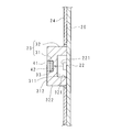
- FIG. 2 is a cross-sectional view schematically showing a main configuration of the light source device according to Embodiment 1.
- FIG. FIG. 6 is a cross-sectional view schematically showing a main configuration of a light source device according to a second embodiment.
- FIG. 10 is a cross-sectional view schematically showing a main configuration of a light source device according to Embodiment 3.
- FIG. 6 is a cross-sectional view schematically showing a main configuration of a light source device according to Embodiment 4.
- FIG. 10 is a cross-sectional view schematically showing a main configuration of a light source device according to Embodiment 5.
- FIG. 1 is a cross-sectional view schematically showing the configuration of the display device 1 according to the first embodiment.
- FIG. 2 is a cross-sectional view schematically showing a main configuration of the light source device 2 according to the first embodiment.
- the display device 1 includes a display panel 11 and a light source device 2.
- the display panel 11 is a light transmissive liquid crystal display panel.
- the light source device 2 includes a box 21, a plurality of light sources 22, a plurality of optical members 23, a reflection sheet 24, a diffusion plate 25, and a light source substrate 26.
- the box 21 has a bottom wall 211 and a peripheral wall 212.
- Each light source 22 is, for example, an LED that emits blue light.
- the light source 22 is mounted on the mounting surface of the light source substrate 26 with the light emitting surface 221 facing upward.
- the light source substrate 26 on which the plurality of light sources 22 are mounted is attached to the bottom wall 211 so that the light emitting surface 221 of each light source 22 faces the opening side of the box body 21, that is, the display panel 11 side.
- Each optical member 23 covers a part of the plurality of light sources 22 at a predetermined interval.
- each optical member 23 covers one light source 22.
- Each optical member 23 is provided on the outside with respect to the light incident surface as viewed from the corresponding light source, and a light incident surface for entering light emitted from the light source 22 (hereinafter also referred to as a corresponding light source) covered by the optical member 23.
- Each optical member 23 has light diffusibility and emits light diffused inside from the light exit surface.
- the optical member 23 is made of, for example, a synthetic resin.
- the optical member 23 has a predetermined space inside, and one light source 22 is disposed in the space.
- the optical member 23 includes a bottom wall 31 and a side wall 32 erected from the periphery of the bottom wall 31, and is in a space surrounded by the inner surface 311 of the bottom wall 31 and the inner surface 321 of the side wall 32.
- One light source 22 is disposed in each.
- the shape of the bottom wall 31 in plan view is, for example, a circle, an ellipse, or a rectangle.
- the optical member 23 has a bottomed cylindrical shape.
- the inner surface 311 of the bottom wall 31 and the outer surface 312 of the bottom wall 31 are flat surfaces parallel to each other, for example.
- the optical member 23 is attached to the mounting surface of the light source substrate 26.
- the optical member 23 is attached to the mounting surface so that the end portion of the side wall 32 (the end portion on the side far from the bottom wall 31) abuts the mounting surface of the light source substrate 26.
- the optical member 23 covers the light source 22 so that the inner surface 311 of the bottom wall 31 faces the light source 22.
- the optical axis of the light source 22 is orthogonal to the inner surface 311 of the bottom wall 31.
- the shape of the optical member 23 is not limited to the shape described above.
- the optical member 23 has a plurality of leg portions extending from the end portion of the side wall 32 (the end portion on the side far from the bottom wall 31), and is mounted so that the leg portions abut on the mounting surface of the light source substrate 26. It may be attached to a surface. That is, a gap may be provided between the end of the side wall 32 and the light source substrate 26.
- the inner surface 311 of the bottom wall 31 and the inner surface 321 of the side wall 32 are light incident surfaces of the optical member 23.
- the light emitted from the light source 22 enters the optical member 23 from the light incident surface.
- the outer surface 312 of the bottom wall 31 and the outer surface 322 of the side wall 32 are light exit surfaces of the optical member 23.
- the light that has entered the inside of the optical member 23 is diffused and emitted from the light exit surface of the optical member 23 to the outside of the optical member 23.
- a recess 33 is provided in a region facing the light emitting surface 221 of the corresponding light source on the light emitting surface of the optical member 23 (specifically, the outer surface 312 of the bottom wall 31).
- the bottom surface of the recess 33 is, for example, a flat surface parallel to the inner surface 311 and the outer surface 312 of the bottom wall 31.
- the concave portion 33 is filled with the wavelength converting portion 41 and the sealing portion 42.
- the wavelength conversion unit 41 has a layer shape covering the bottom surface of the recess 33. That is, the wavelength conversion unit 41 is provided in contact with the bottom surface of the recess 33 that is a part of the light output surface of the optical member 23.
- the wavelength conversion unit 41 includes, for example, two types of quantum dots (wavelength conversion body) and a translucent material (for example, titanium oxide) that carries the quantum dots.
- quantum dots wavelength conversion body
- a translucent material for example, titanium oxide
- One type of quantum dot converts the frequency of blue light into the frequency of red light.
- Other types of quantum dots convert blue light frequency to green light frequency.
- the sealing unit 42 reflects the light incident on the wavelength conversion unit 41 toward the optical member 23 and seals the wavelength conversion unit 41.
- the sealing portion 42 has a layered shape laminated on the wavelength conversion portion 41 and closes the opening of the recess 33.
- the sealing part 42 is made of, for example, metal, specifically an aluminum thin film, and has high light reflectivity. As described above, the wavelength conversion unit 41 is sealed by the sealing unit 42, thereby preventing the quantum dots from being deteriorated due to the wavelength conversion unit 41 being exposed to oxygen or moisture.
- the reflection sheet 24 has high light reflectivity.
- the reflection sheet 24 covers the inner surface of the box 21 and the portion of the mounting surface of the light source substrate 26 where the optical member 23 is not provided.
- the diffusion plate 25 has light diffusibility.
- the diffusion plate 25 is made of, for example, a synthetic resin.
- the diffusion plate 25 is attached to the peripheral wall 212 of the box body 21 so as to close the opening of the box body 21 from the inside of the box body 21.
- the peripheral wall 212 is provided with a step portion that supports the peripheral portion of the diffusion plate 25.
- Blue light emitted from the light source 22 enters the optical member 23 from the light incident surface of the optical member 23.
- Part of the blue light that has entered the inside of the optical member 23 is converted into red light and green light by entering the quantum dots included in the wavelength conversion unit 41.
- Light incident on the quantum dots is scattered.
- Part of the scattered light enters the optical member 23 again.
- Another part of the scattered light is reflected by the sealing portion 42 toward the optical member 23. That is, the light incident on the wavelength conversion unit 41 is suppressed from being emitted directly to the outside of the optical member 23.
- the other part of the blue light that has entered the optical member 23 remains blue light. Therefore, red light, green light, and blue light are diffused and mixed inside the optical member 23 to become white light without color unevenness. As a result, white light having no color unevenness is emitted from the light exit surface of the optical member 23.
- the wavelength conversion unit 41 faces the light exit surface 221 of the light source 22. Therefore, the blue light emitted from the light source 22 (see the broken arrow shown in FIG. 2) is easily incident on the wavelength conversion unit 41. Accordingly, a sufficient amount of red light and green light can be obtained, so that occurrence of color unevenness in white light due to a shortage of red light or green light is suppressed.
- the wavelength converting part 41 is sealed in a space surrounded by the inner surface of the recess 33 and the sealing part 42. Therefore, the quantum dots included in the wavelength conversion unit 41 can be reliably protected from, for example, oxygen or moisture. Moreover, since the wavelength conversion part 41 and the sealing part 42 are distribute
- the light emitted from the light exit surface of the optical member 23 is directly incident on the diffusion plate 25 or is reflected by the reflection sheet 24 and then enters the diffusion plate 25.
- the light incident on the diffusion plate 25 is diffused. As a result, uniform light is emitted from the light source device 2 in the surface direction of the diffusion plate 25.
- the display panel 11 is attached to the peripheral wall 212 of the box 21 so as to close the opening of the box 21 from the outside of the box 21.
- the optical sheet group 12 is disposed between the display panel 11 and the diffusion plate 25.
- the optical sheet group 12 is formed by laminating a plurality of optical sheets each having optical transparency. Each optical sheet has, for example, a light diffusion function, a light collection function, or a polarization function.
- a spacer 13 is interposed between the peripheral edge of the optical sheet group 12 and the peripheral edge of the diffusion plate 25.
- the spacer 13 has a frame shape and has a non-light-transmitting property and a buffering property.
- the light source device 2 functions as a so-called direct type backlight.
- the light emitted from the light source device 2 is transmitted through the optical sheet group 12, and the light transmitted through the optical sheet group 12 enters the display panel 11.
- the light that has entered the display panel 11 passes through the display panel 11 or is blocked by the display panel 11, an image is displayed on the display panel 11.
- the light source 22 generates heat with light emission.
- the wavelength converter 41 is provided on the optical member 23.
- an air gap is provided between the optical member 23 and the corresponding light source. Therefore, the wavelength converter 41 can be separated from the light source 22. Therefore, the heat generated by the light source 22 is not easily transmitted to the wavelength conversion unit 41. As a result, deterioration of the quantum dots included in the wavelength conversion unit 41 due to heat can be suppressed.
- the light source 22 and the optical member 23 have a one-to-one correspondence. Therefore, the area of the surface that receives the light in the wavelength conversion unit 41 can be reduced. Accordingly, it is possible to reduce the total amount of quantum dots included in the wavelength conversion unit 41 provided in the plurality of optical members 23. As a result, the manufacturing cost of the light source device 2 can be reduced.
- the light source 22 and the optical member 23 do not necessarily have a one-to-one correspondence, and one optical member 23 covers a plurality of (for example, two) light sources 22 within a range where the area of the wavelength conversion unit 41 does not increase. May be.
- the light source 22 is not limited to an LED, and may be an LD (Laser Diode), for example.
- the light emitted from the LD has high directivity. Therefore, when the LD is used, the area of the wavelength conversion unit 41 can be made smaller than when the LED is used, and the amount of quantum dots contained in the wavelength conversion unit 41 can be further reduced. Further, since blue light emitted from the LD has high color purity, white light with high color purity can be obtained.
- the wavelength conversion unit 41 may include a quantum dot that converts the frequency of blue light into the frequency of yellow light. Further, the color of light emitted from the light source 22 is not limited to blue, and may be purple, for example. In this case, the wavelength conversion unit 41 includes a quantum dot that converts the frequency of the violet light into the frequency of the red light, a quantum dot that converts the frequency of the violet light into the frequency of the green light, and the frequency of the violet light of the blue light. Quantum dots that convert to frequency are included. Further, the wavelength conversion unit 41 may include a light emitter instead of the quantum dots.
- the inner surface 311 and the outer surface 312 of the bottom wall 31 of the optical member 23 are not limited to flat surfaces parallel to each other, and may be, for example, a convex spherical surface or an inclined flat surface.
- the optical member 23 is not limited to a bottomed cylindrical shape, and may be a dome shape, for example.
- the recess 33 is not limited to the outer surface 312 of the bottom wall 31, and may be provided on the outer surface 322 of the side wall 32.
- the light source device 2 according to the second to fourth embodiments is provided in the display device 1 according to the first embodiment, similarly to the light source device 2 according to the first embodiment.
- the light source device 2 according to the second to fourth embodiments has the same effects as the light source device 2 according to the first embodiment.
- differences from the light source device 2 of the first embodiment will be mainly described, and the same components as those of the light source device 2 of the first embodiment are denoted by the same reference numerals and description thereof will be omitted.
- FIG. 3 is a cross-sectional view schematically showing a main configuration of the light source device 2 according to the second embodiment.
- the optical member 23 is not provided with a recess 33.
- the wavelength conversion unit 41 is provided in contact with a region facing the light exit surface 221 of the corresponding light source on the light exit surface of the optical member 23 (specifically, the outer surface 312 of the bottom wall 31).
- the sealing unit 42 seals the wavelength conversion unit 41.
- the area of the wavelength conversion unit 41 can be increased, and the light emitted from the light source 22 is incident on the wavelength conversion unit 41. Can be made easier.
- FIG. 4 is a cross-sectional view schematically showing a main configuration of the light source device 2 according to the third embodiment.
- the concave portion 33 of the optical member 23 according to the present embodiment is formed shallower than the concave portion 33 of the optical member 23 according to the first embodiment.
- the whole recessed part 33 is filled with the wavelength conversion part 41, and the wavelength conversion part 41 is sealed by the sealing part 42 from the top.
- the sealing part 42 seals the wavelength conversion part 41 and covers the peripheral part of the opening of the recess 33 in the outer surface 312 of the bottom wall 31 of the optical member 23.
- the distance between the wavelength conversion unit 41 and the optical member 23 can be made wider than that in the first embodiment. Therefore, deterioration of the quantum dots included in the wavelength conversion unit 41 due to heat can be more effectively suppressed.
- FIG. 5 is a cross-sectional view schematically showing a main configuration of the light source device 2 according to the fourth embodiment.
- the light source device 2 according to the present embodiment collects light emitted from the light source 22 in the wavelength conversion unit 41 between the light source 22 and the wavelength conversion unit 41 provided in the optical member 23 covering the light source 22.
- a light unit 27 is provided.
- the condensing part 27 is a semi-convex lens, for example, and has a plane and a spherical surface.
- the light collecting unit 27 is attached to the light source 22 so that the plane of the light collecting unit 27 covers the light emitting surface 221 of the light source 22.
- the light emitted from the light source 22 is collected by the light collecting unit 27 (see the broken arrow), the light emitted from the light source 22 can be easily incident on the wavelength converting unit 41.
- the light collecting unit 27 may be attached to the light source 22 of the first to third embodiments.
- the light source device 2 seals the wavelength conversion unit 41 and the reflection unit 44 that reflects the light incident on the wavelength conversion unit 41 toward the optical member 23 instead of the sealing unit 42.
- the sealing part 43 to be provided.
- the concave portion 33 is filled with the wavelength converting portion 41, the sealing portion 43, and the reflecting portion 44.
- the reflection unit 44 has a layered shape laminated on the wavelength conversion unit 41.
- the reflecting portion 44 is made of, for example, a metal, specifically an aluminum thin film, and has high light reflectivity.
- the sealing portion 43 has a layered shape laminated on the reflecting portion 44 and closes the opening of the concave portion 33.
- the sealing part 43 is made of, for example, a synthetic resin genus.
- the light incident on the quantum dots included in the wavelength conversion unit 41 is scattered. Part of the scattered light enters the optical member 23 again. Another part of the scattered light is reflected toward the optical member 23 by the reflecting portion 44. That is, the light incident on the wavelength conversion unit 41 is suppressed from being emitted directly to the outside of the optical member 23. Therefore, red light, green light, and blue light are diffused and mixed inside the optical member 23 to become white light with no color unevenness. As a result, white light having no color unevenness is emitted from the light exit surface of the optical member 23.
- the sealing part 43 may be distribute
- the reflection part 44 is distribute
- the wavelength conversion part 41 may be provided in the outer surface 312 of the bottom wall 31 of the optical member 23 like the wavelength conversion part 41 shown in FIG. In this case, the laminated body of the sealing part 43 and the reflection part 44 may cover the wavelength conversion part 41 so that the sealing part 42 shown in FIG.
- the sealing portion 43 and the reflecting portion 44 may be reversed. That is, the sealing unit 43 may be stacked on the wavelength conversion unit 41, and the reflection unit 44 may be stacked on the sealing unit 43.
- the sealing portion 43 is light transmissive. Part of the light incident on the wavelength conversion unit 41 is transmitted through the sealing unit 43, and the light transmitted through the sealing unit 43 is reflected toward the optical member 23 by the reflection unit 44.
- the wavelength conversion unit 41 may be sealed inside the sealing unit 43. Further, a plurality of layered or non-layered wavelength conversion parts 41 may be scattered and sealed inside the sealing part 43.
- FIG. 6 is a cross-sectional view schematically showing a main configuration of the light source device 2 according to the fifth embodiment.
- the light source device 2 according to the present embodiment has the same configuration as that of the light source device 2 according to the fourth embodiment, except that a light collecting unit 34 is provided instead of the light collecting unit 27.
- a light collecting unit 34 is provided instead of the light collecting unit 27.
- the light source device 2 of the present embodiment collects light emitted from the light source 22 in the wavelength conversion unit 41 between the light source 22 and the wavelength conversion unit 41 provided on the optical member 23 covering the light source 22.
- the unit 34 is provided.
- the condensing part 34 is provided on the inner surface 311 of the bottom wall 31 of the optical member 23.
- the condensing part 34 is, for example, a convex part having a semi-convex lens shape, and projects from the inner surface 311 toward the light source 22.
- the light emitted from the light source 22 is converted into the wavelength as in the fourth embodiment. It can make it easy to enter into the conversion part 41.
- FIG. The condensing unit 34 may be provided in the optical member 23 of the first to third embodiments.
- the light source device 2 covers the plurality of light sources 22 and each of the light sources 22 of the plurality of light sources 22 at a predetermined interval.
- Light entrance surfaces 311 and 321 for entering emitted light, and light exit surfaces 312 and 322 provided outside the light entrance surfaces 311 and 321 when viewed from the part of the light sources 22.
- the wavelength conversion unit 41 can be appropriately separated from the light source 22, and deterioration of the wavelength conversion body included in the wavelength conversion unit 41 due to heat can be suppressed. Moreover, the area of the surface which receives the light in the wavelength conversion part 41 can be made small, and the usage-amount of a wavelength converter can be reduced.
- the light source device 2 may further include a sealing unit 42 that reflects the light incident on the wavelength conversion unit 41 toward the optical member 23 and seals the wavelength conversion unit 41. .
- a sealing unit 42 that reflects the light incident on the wavelength conversion unit 41 toward the optical member 23 and seals the wavelength conversion unit 41.
- the light scattered by the wavelength conversion unit 41 is reflected by the sealing unit 42 toward the optical member 23. Therefore, mixing of light by the optical member 23 can be promoted, and color unevenness of light emitted from the optical member 23 can be suppressed.
- the wavelength conversion part 41 is sealed by the sealing part 42, the wavelength conversion part 41 can be protected from the substance which degrades the wavelength converter contained in the wavelength conversion part 41, for example.
- the light source device 2 further includes a reflection unit 44 that reflects the light incident on the wavelength conversion unit 41 toward the optical member 23, and a sealing unit 43 that seals the wavelength conversion unit 41.
- a reflection unit 44 that reflects the light incident on the wavelength conversion unit 41 toward the optical member 23, and a sealing unit 43 that seals the wavelength conversion unit 41.
- the wavelength conversion unit 41 may be provided in a region of the light exit surfaces 312 and 322 facing the light exit surface 221 of the partial light source 22. According to the above configuration, the light emitted from the light source 22 can be easily incident on the wavelength conversion unit 41.
- a concave portion 33 is provided in a region of the light emitting surfaces 312 and 322 facing the light emitting surface 221 of the part of the light sources 22, and the wavelength conversion unit 41 includes the concave portion. 33 may be provided. According to the above configuration, the light emitted from the light source 22 can be easily incident on the wavelength conversion unit 41, and the wavelength conversion unit 41 is disposed inside the recess 33, so that the wavelength conversion unit 41 collides with other members, for example. Can be protected from.
- a condensing unit 27 that collects light emitted from the partial light sources 22 in the wavelength conversion unit 41 between the partial light sources 22 and the wavelength conversion unit 41. 34 may be further provided. According to the above configuration, the light emitted from the light source 22 can be efficiently incident on the wavelength conversion unit 41.
- the optical member 23 includes a bottom wall 31 and a side wall 32 erected from the periphery of the bottom wall 31, and the inner surface 311 of the bottom wall 31 and the inner surface of the side wall 32.
- 321 covers the part of the light source 22, the inner surface 311 of the bottom wall 31 and the inner surface 321 of the side wall 32 are the light incident surfaces, and the outer surface 312 of the bottom wall 31 and the outer surface 322 of the side wall 32 are It may be the light exit surface.
- the display device 1 includes the light source device 2 according to the above-described embodiment and the display panel 11 illuminated by the light source device 2.
- the wavelength conversion unit 41 can be appropriately separated from the light source 22, and deterioration of the wavelength converter included in the wavelength conversion unit 41 due to heat can be suppressed. Moreover, the area of the surface which receives the light in the wavelength conversion part 41 can be made small, and the usage-amount of a wavelength converter can be reduced. Therefore, the display apparatus 1 which can suppress deterioration by the heat
- the light source device 2 which concerns on embodiment is not limited to the light source device 2 integrated in the display apparatus 1,
- deterioration of the wavelength converter included in the wavelength conversion unit 41 due to heat can be suppressed.
- the usage-amount of the wavelength conversion body contained in the wavelength conversion part 41 can be reduced.
- the display device 1 or the light source device 2 may include components that are not disclosed in the first to fifth embodiments.
- the constituent elements (technical features) disclosed in each embodiment can be combined with each other, and a new technical feature can be formed by the combination.
Landscapes
- Engineering & Computer Science (AREA)
- General Engineering & Computer Science (AREA)
- Led Device Packages (AREA)
- Planar Illumination Modules (AREA)
Abstract
光源装置は、複数の光源と、複数の光学部材と、波長変換部とを備える。複数の光学部材は、夫々が複数の光源のうちの一部の光源を所定間隔を隔てて覆い、該一部の光源が発した光を内部に入れる入光面と、該一部の光源から見て入光面よりも外側に設けられた出光面とを有し、内部で拡散した光を出光面から放出する。波長変換部は、光学部材の出光面の一部に接して設けられ、光の周波数を変換する。
Description
本発明は、光源装置及び該光源装置を備える表示装置に関する。
従来、白色光を発する白色光源が知られている。白色光源は、例えば、青色光を発するLED(Light Emitting Diode)と青色光の周波数を変換する波長変換部とを、1つのパッケージに内包している。波長変換部には、例えば青色光の波長を黄色光の波長に変換する波長変換体(例えば発光体)が含まれている。白色光源は、青色光と波長変換体によって変換された黄色光との混合光(白色光)をパッケージの外部へ放出する。
近年、波長変換体として量子ドットを用いることが提案されている。量子ドットには、色純度が高い光が得られるという利点、及び、量子ドットのサイズを変えれば変換後の波長を容易に選定することができるという利点がある。しかしながら、LEDと量子ドットを含む波長変換部とを1つのパッケージに内包した場合、LEDが発する熱を受けて量子ドットが劣化する虞がある。
例えば、特許文献1には、量子ドットを含むシート状の波長変換部を備えた直下型の光源装置が開示されている。この光源装置では、光源と波長変換部とが離隔して配置されているので、量子ドットの熱による劣化が抑制される。
しかしながら、特許文献1に記載されている光源装置では、波長変換部が複数の光源を覆うシート状でありその面積は大きい。従って、波長変換部に含まれる量子ドットの量は多い。一般に、量子ドットは高価なので、シート状の波長変換部を備えた光源装置の製造コストは高くなる。以上のような問題は、量子ドットに限定されず、熱に弱く高価な発光体を用いる場合にも起こり得る。
本発明は斯かる事情に鑑みてなされたものであり、その主たる目的は、波長変換体の熱による劣化を抑制でき且つ波長変換体の使用量を低減できる光源装置及び表示装置を提供することにある。
本実施の形態に係る光源装置は、複数の光源と、夫々が前記複数の光源のうちの一部の光源を所定間隔を隔てて覆い、該一部の光源が発した光を内部に入れる入光面と、前記一部の光源から見て前記入光面よりも外側に設けられた出光面とを有し、内部で拡散した光を前記出光面から放出する複数の光学部材と、該光学部材の前記出光面の一部に接して設けられ、光の周波数を変換する波長変換部とを備えることを特徴とする。
本実施の形態に係る表示装置は、本実施の形態に係る光源装置と、該光源装置によって照明される表示パネルとを備えることを特徴とする。
本発明によれば、波長変換体の熱による劣化を抑制でき且つ波長変換体の使用量を低減できる光源装置及び表示装置が提供される。
以下、本発明の実施の形態について図面に基づいて詳述する。
(実施の形態1)
図1は、実施の形態1に係る表示装置1の構成を略示する断面図である。図2は、実施の形態1に係る光源装置2の要部構成を略示する断面図である。表示装置1は、表示パネル11及び光源装置2を備える。表示パネル11は、光透過型の液晶表示パネルである。光源装置2は、箱体21、複数の光源22、複数の光学部材23、反射シート24、拡散板25、及び光源基板26を備える。
図1は、実施の形態1に係る表示装置1の構成を略示する断面図である。図2は、実施の形態1に係る光源装置2の要部構成を略示する断面図である。表示装置1は、表示パネル11及び光源装置2を備える。表示パネル11は、光透過型の液晶表示パネルである。光源装置2は、箱体21、複数の光源22、複数の光学部材23、反射シート24、拡散板25、及び光源基板26を備える。
箱体21は、底壁211と周壁212とを有する。各光源22は、例えば青色光を発するLEDである。光源22は、光源基板26の実装面にその光出射面221を上向きにして実装されている。複数の光源22が実装された光源基板26は、各光源22の光出射面221が箱体21の開口側、即ち表示パネル11側を向くように、底壁211に取り付けられている。
各光学部材23は、複数の光源22のうちの一部の光源22を所定間隔を隔てて覆っている。本実施の形態では、各光学部材23が1つの光源22を覆っている。各光学部材23は、該光学部材23が覆っている光源22(以下、対応光源ともいう)が発した光を内部に入れる入光面と、対応光源から見て入光面よりも外側に設けられた出光面とを有する。各光学部材23は、光拡散性を有し、内部で拡散した光を出光面から放出する。光学部材23は、例えば合成樹脂製である。
本実施の形態において、光学部材23は、内側に所定の空間を有し、その空間内に1つの光源22が配置される。具体的には、光学部材23は、底壁31と、底壁31の周縁から立設した側壁32とを有し、底壁31の内面311と側壁32の内面321とに囲まれた空間内に1つの光源22が配置される。底壁31の平面視の形状は、例えば、円形、楕円形、矩形等であり、底壁31が平面視円形の場合は、光学部材23は有底円筒状をなす。底壁31の内面311及び底壁31の外面312は、例えば互いに平行な平坦面である。
光学部材23は、光源基板26の実装面に取り付けられている。例えば、光学部材23は、その側壁32の端部(底壁31から遠い側の端部)が光源基板26の実装面に当接するように実装面に取り付けられる。光学部材23は、底壁31の内面311が光源22に対向するようにして、光源22を覆っている。光源22の光軸は、底壁31の内面311に直交する。なお、光学部材23の形状は、上述した形状に限定されない。例えば、光学部材23は、その側壁32の端部(底壁31から遠い側の端部)から延びる複数の脚部を有し、該脚部が光源基板26の実装面に当接するように実装面に取り付けられてもよい。即ち、側壁32の端部と光源基板26との間に隙間が設けられていてもよい。
底壁31の内面311及び側壁32の内面321は、光学部材23の入光面である。光源22が発した光は、入光面から光学部材23の内部に進入する。底壁31の外面312及び側壁32の外面322は、光学部材23の出光面である。光学部材23の内部に進入した光は拡散されて、光学部材23の出光面から光学部材23の外部に放出される。
本実施の形態において、光学部材23の出光面(具体的には、底壁31の外面312)における対応光源の光出射面221に対向する領域には、凹部33が設けられている。凹部33の底面は、例えば底壁31の内面311及び外面312に平行な平坦面である。凹部33は、波長変換部41及び封止部42によって埋められている。
波長変換部41は、凹部33の底面を覆う層状をなす。即ち、波長変換部41は、光学部材23の出光面の一部である凹部33の底面に接して設けられている。波長変換部41には、例えば2種類の量子ドット(波長変換体)と、量子ドットを担持する透光性物質(例えば酸化チタン)とが含まれている。一の種類の量子ドットは、青色光の周波数を赤色光の周波数に変換する。他の種類の量子ドットは、青色光の周波数を緑色光の周波数に変換する。
封止部42は、波長変換部41に入射した光を光学部材23に向けて反射させると共に、波長変換部41を封止する。封止部42は、波長変換部41に積層された層状をなし、凹部33の開口を閉塞している。封止部42は、例えば金属製、具体的にはアルミ薄膜等であり、高い光反射性を有する。このように、波長変換部41が封止部42によって封止されることで、波長変換部41が酸素又は水分に曝されることによる量子ドットの劣化を防止できる。
反射シート24は、高い光反射性を有する。反射シート24は、箱体21の内面、及び光源基板26の実装面における光学部材23が設けられていない部分を覆っている。
拡散板25は光拡散性を有する。拡散板25は例えば合成樹脂製である。拡散板25は、箱体21の開口を箱体21の内側から閉塞するようにして、箱体21の周壁212に取り付けられている。周壁212には、拡散板25の周縁部を支持する段部が設けられている。
光源22が発した青色光は、光学部材23の入光面から光学部材23の内部に進入する。光学部材23の内部に進入した青色光の一部は、波長変換部41に含まれている量子ドットに入射することによって、赤色光及び緑色光に変換される。量子ドットに入射した光は散乱する。散乱した光の一部は、光学部材23の内部に再び進入する。散乱した光の他の一部は、封止部42によって、光学部材23に向けて反射される。つまり、波長変換部41に入射した光が、直接的に光学部材23の外部に放出されることが抑制される。光学部材23の内部に進入した青色光の他の一部は、青色光のままである。故に、赤色光、緑色光、及び青色光は、光学部材23の内部で拡散及び混合されて、色ムラのない白色光になる。その結果、色ムラのない白色光が、光学部材23の出光面から放出される。
波長変換部41は、光源22の光出射面221に対向している。故に、光源22が発した青色光(図2に示す破線の矢符参照)は、波長変換部41に入射し易い。従って、十分な量の赤色光及び緑色光を得ることができるので、赤色光又は緑色光の量が不足することによって白色光に色ムラが生じることが抑制される。
波長変換部41は、凹部33の内面と封止部42とに囲まれた空間にて封止される。故に、波長変換部41に含まれている量子ドットを例えば酸素又は水分から確実に保護することができる。また、波長変換部41及び封止部42が凹部33の内部に配されているので、波長変換部41及び封止部42を、例えば他部材との衝突から保護することができる。
光学部材23の出光面から放出された光は、直接的に拡散板25に入射するか、又は、反射シート24に反射されてから拡散板25に入射する。拡散板25に入射した光は拡散される。この結果、光源装置2から拡散板25の面方向に均一な光が放出される。
表示パネル11は、箱体21の開口を箱体21の外側から閉塞するようにして、箱体21の周壁212に取り付けられている。表示パネル11と拡散板25との間には、光学シート群12が配されている。光学シート群12は、夫々光透過性を有する複数枚の光学シートが積層されたものである。各光学シートは、例えば光拡散機能、集光機能、又は偏光機能を有する。光学シート群12の周縁部と拡散板25の周縁部との間にはスペーサ13が介在している。スペーサ13は枠状をなし、非透光性及び緩衝性を有する。
光源装置2は、いわゆる直下型のバックライトとして機能する。光源装置2から放出された光は、光学シート群12を透過し、光学シート群12を透過した光は、表示パネル11の内部に進入する。表示パネル11の内部に進入した光が表示パネル11を透過するか表示パネル11によって遮断されることによって、表示パネル11に映像が表示される。
ところで、光源22は発光に伴って発熱する。しかしながら、波長変換部41は光学部材23に設けられている。しかも、光学部材23と対応光源との間にはエアーギャップが設けられている。故に、波長変換部41を光源22から離隔させることができる。従って、光源22が発した熱は波長変換部41に伝わり難い。この結果、波長変換部41に含まれている量子ドットの熱による劣化を抑制することができる。
本実施の形態において、光源22と光学部材23(波長変換部41)とは一対一対応である。故に、波長変換部41における光を受ける面の面積を小さくすることができる。従って、複数の光学部材23に設けられた波長変換部41に含まれている量子ドットの総量を低減することができる。この結果、光源装置2の製造コストを低減することができる。なお、光源22と光学部材23とは必ずしも一対一対応でなくともよく、波長変換部41の面積が大きくならない範囲で、1つの光学部材23が複数(例えば2つ)の光源22を覆うようにしてもよい。
なお、光源22はLEDに限定されず、例えばLD(Laser Diode )でもよい。LDが発する光は指向性が高い。故に、LDを用いた場合は、LEDを用いる場合よりも波長変換部41の面積を小さくすることができ、波長変換部41に含まれる量子ドットの量を更に低減することができる。また、LDが発する青色光は色純度が高いので、色純度が高い白色光を得ることができる。
また、波長変換部41には、青色光の周波数を黄色光の周波数に変換する量子ドットが含まれていてもよい。また、光源22が発する光の色は青色に限定されず、例えば紫色であってもよい。この場合、波長変換部41には、紫色光の周波数を赤色光の周波数に変換する量子ドット、紫色光の周波数を緑色光の周波数に変換する量子ドット、及び、紫色光の周波数を青色光の周波数に変換する量子ドットが含まれる。また、波長変換部41は、量子ドットに代えて発光体を含んでいてもよい。
また、光学部材23の底壁31の内面311及び外面312は、互いに平行な平坦面に限定されず、例えば凸状の球面、又は傾斜した平坦面でもよい。光学部材23は有底筒状に限定されず、例えばドーム状でもよい。凹部33は、底壁31の外面312に限定されず、側壁32の外面322に設けられてもよい。
次に、実施の形態2~4の光源装置2について説明する。実施の形態2~4の光源装置2は、実施の形態1の光源装置2と同様に、実施の形態1の表示装置1に備えられる。実施の形態2~4の光源装置2は、実施の形態1の光源装置2と同様の作用効果を奏する。以下では、主に実施の形態1の光源装置2との差異について説明し、実施の形態1の光源装置2と同一の構成要素には同一符号を付してそれらの説明を省略する。
(実施の形態2)
図3は、実施の形態2に係る光源装置2の要部構成を略示する断面図である。光学部材23には凹部33が設けられていない。本実施の形態において、波長変換部41は、光学部材23の出光面(具体的には、底壁31の外面312)における対応光源の光出射面221に対向する領域に接して設けられている。封止部42は、波長変換部41を封止する。
図3は、実施の形態2に係る光源装置2の要部構成を略示する断面図である。光学部材23には凹部33が設けられていない。本実施の形態において、波長変換部41は、光学部材23の出光面(具体的には、底壁31の外面312)における対応光源の光出射面221に対向する領域に接して設けられている。封止部42は、波長変換部41を封止する。
実施の形態2によれば、底壁31の外面312は凹部33の底面より広いので、波長変換部41の面積を大きくすることができ、光源22が発した光を波長変換部41に入射し易くすることができる。
(実施の形態3)
図4は、実施の形態3に係る光源装置2の要部構成を略示する断面図である。本実施の形態に係る光学部材23の凹部33は、実施の形態1に係る光学部材23の凹部33よりも浅く形成されている。そして、凹部33の全体が波長変換部41によって埋められ、波長変換部41がその上から封止部42によって封止されている。封止部42は、波長変換部41を封止すると共に、光学部材23の底壁31の外面312における凹部33の開口の周辺部分を覆う。
図4は、実施の形態3に係る光源装置2の要部構成を略示する断面図である。本実施の形態に係る光学部材23の凹部33は、実施の形態1に係る光学部材23の凹部33よりも浅く形成されている。そして、凹部33の全体が波長変換部41によって埋められ、波長変換部41がその上から封止部42によって封止されている。封止部42は、波長変換部41を封止すると共に、光学部材23の底壁31の外面312における凹部33の開口の周辺部分を覆う。
実施の形態3によれば、実施の形態1の場合に比べて、波長変換部41と光学部材23との間隔をより広くすることができる。よって、波長変換部41に含まれている量子ドットの熱による劣化をより効果的に抑制することができる。
(実施の形態4)
図5は、実施の形態4に係る光源装置2の要部構成を略示する断面図である。本実施の形態に係る光源装置2は、光源22と該光源22を覆う光学部材23に設けられた波長変換部41との間に、該光源22が発した光を波長変換部41に集める集光部27を備える。集光部27は、例えば半凸レンズであり、平面と球面とを有する。集光部27は、集光部27の平面が光源22の光出射面221を覆うように、光源22に取り付けられている。
図5は、実施の形態4に係る光源装置2の要部構成を略示する断面図である。本実施の形態に係る光源装置2は、光源22と該光源22を覆う光学部材23に設けられた波長変換部41との間に、該光源22が発した光を波長変換部41に集める集光部27を備える。集光部27は、例えば半凸レンズであり、平面と球面とを有する。集光部27は、集光部27の平面が光源22の光出射面221を覆うように、光源22に取り付けられている。
実施の形態4によれば、光源22が発した光が集光部27によって集められる(破線の矢符参照)ので、光源22が発した光を波長変換部41に入射し易くすることができる。なお、集光部27は、実施の形態1~3の光源22に取り付けられていてもよい。
また、本実施の形態に係る光源装置2は、封止部42の代わりに、波長変換部41に入射した光を光学部材23に向けて反射させる反射部44と、波長変換部41を封止する封止部43とを備える。凹部33は、波長変換部41、封止部43、及び反射部44によって埋められている。反射部44は、波長変換部41に積層された層状をなす。反射部44は、例えば金属製、具体的にはアルミ薄膜等であり、高い光反射性を有する。封止部43は、反射部44に積層された層状をなし、凹部33の開口を閉塞している。封止部43は、例えば合成樹脂属製である。
波長変換部41に含まれている量子ドットに入射した光は散乱する。散乱した光の一部は、光学部材23の内部に再び進入する。散乱した光の他の一部は、反射部44によって光学部材23に向けて反射される。つまり、波長変換部41に入射した光が、直接的に光学部材23の外部に放出されることが抑制される。従って、赤色光、緑色光、及び青色光が、光学部材23の内部で拡散及び混合されて色ムラのない白色光になる。その結果、色ムラのない白色光が、光学部材23の出光面から放出される。
なお、封止部43が、図4に示す封止部42のように、凹部33の外部に配されていてもよい。また、反射部44が、図4に示す封止部42のように凹部33の外部に配され、封止部43が、図3に示す封止部42のように、反射部44を覆っていてもよい。また、波長変換部41が、図3に示す波長変換部41のように、光学部材23の底壁31の外面312に設けられていてもよい。この場合、封止部43及び反射部44の積層体が、図3に示す封止部42が波長変換部41を覆うように、波長変換部41を覆えばよい。
更に、封止部43と反射部44との配置が逆でもよい。即ち、封止部43が波長変換部41に積層され、反射部44が封止部43に積層されてもよい。この場合、封止部43は光透過性を有している。波長変換部41に入射した光の一部は封止部43を透過し、封止部43を透過した光は、反射部44によって、光学部材23に向けて反射される。
また、波長変換部41は、封止部43の内部に封止されていてもよい。また、複数の層状又は非層状の波長変換部41が、封止部43の内部に散在して封止されていてもよい。
(実施の形態5)
図6は、実施の形態5に係る光源装置2の要部構成を略示する断面図である。本実施の形態の光源装置2は、集光部27の代わりに集光部34が設けられている点を除き、実施の形態4の光源装置2と同様の構成である。以下、主に実施の形態4の光源装置2との差異について説明する。
図6は、実施の形態5に係る光源装置2の要部構成を略示する断面図である。本実施の形態の光源装置2は、集光部27の代わりに集光部34が設けられている点を除き、実施の形態4の光源装置2と同様の構成である。以下、主に実施の形態4の光源装置2との差異について説明する。
本実施の形態の光源装置2は、光源22と該光源22を覆う光学部材23に設けられた波長変換部41との間に、該光源22が発した光を波長変換部41に集める集光部34を備える。集光部34は、光学部材23の底壁31の内面311に設けられている。集光部34は、例えば半凸レンズ状の凸部であり、内面311から光源22に向けて突出している。
実施の形態5によれば、光源22が発した光の一部が集光部34によって集められる(破線の矢符参照)ので、実施の形態4と同様に、光源22が発した光を波長変換部41に入射し易くすることができる。なお、集光部34は、実施の形態1~3の光学部材23に設けられていてもよい。
以上、本発明の幾つかの実施の形態について説明した。このように、実施の形態に係る光源装置2は、複数の光源22と、夫々が前記複数の光源22のうちの一部の光源22を所定間隔を隔てて覆い、該一部の光源22が発した光を内部に入れる入光面311,321と、前記一部の光源22から見て前記入光面311,321よりも外側に設けられた出光面312,322とを有し、内部で拡散した光を前記出光面312,322から放出する複数の光学部材23と、該光学部材23の前記出光面312,322の一部に接して設けられ、光の周波数を変換する波長変換部41とを備える。
上記構成によれば、波長変換部41を光源22から適宜に離隔させることができ、波長変換部41に含まれている波長変換体の熱による劣化を抑制することができる。また、波長変換部41における光を受ける面の面積を小さくすることができ、波長変換体の使用量を低減することができる。
実施の形態に係る光源装置2は、前記波長変換部41に入射した光を前記光学部材23に向けて反射させると共に、前記波長変換部41を封止する封止部42を更に備えてもよい。上記構成によれば、波長変換部41にて散乱した光が封止部42によって光学部材23に向けて反射される。故に、光学部材23による光の混合を促進することができ、光学部材23から放出される光の色ムラを抑制することができる。また、波長変換部41は封止部42によって封止されるので、例えば、波長変換部41に含まれている波長変換体を劣化させる物質から波長変換部41を保護することができる。
実施の形態に係る光源装置2は、前記波長変換部41に入射した光を前記光学部材23に向けて反射させる反射部44と、前記波長変換部41を封止する封止部43とを更に備えてもよい。すなわち、反射機能を有する反射部44と、封止機能を有する封止部43とが別々に設けられてもよい。上記構成によれば、反射機能及び封止機能を有する封止部42を設ける場合と同様の効果が得られる。
実施の形態に係る光源装置2において、前記波長変換部41は、前記出光面312,322における前記一部の光源22の光出射面221に対向する領域に設けられていてもよい。上記構成によれば、光源22が発した光を波長変換部41に入射し易くすることができる。
実施の形態に係る光源装置2において、前記出光面312,322における前記一部の光源22の光出射面221に対向する領域に凹部33が設けられており、前記波長変換部41は、前記凹部33の内部に設けられていてもよい。上記構成によれば、光源22が発した光を波長変換部41に入射し易くできると共に、波長変換部41が凹部33の内側に配されるので、波長変換部41を例えば他部材との衝突から保護することができる。
実施の形態に係る光源装置2は、前記一部の光源22と前記波長変換部41との間に、前記一部の光源22が発した光を前記波長変換部41に集める集光部27,34を更に備えてもよい。上記構成によれば、光源22が発した光を波長変換部41に効率よく入射させることができる。
実施の形態に係る光源装置2において、前記光学部材23は、底壁31と該底壁31の周縁から立設した側壁32とを有し、前記底壁31の内面311及び前記側壁32の内面321で前記一部の光源22を覆っており、前記底壁31の内面311及び前記側壁32の内面321が前記入光面であり、前記底壁31の外面312及び前記側壁32の外面322が前記出光面であってもよい。
実施の形態に係る表示装置1は、上述した実施の形態に係る光源装置2と、該光源装置2によって照明される表示パネル11とを備える。
上記構成によれば、実施の形態に係る光源装置2によって次の効果が得られる。すなわち、波長変換部41を光源22から適宜に離隔させることができ、波長変換部41に含まれている波長変換体の熱による劣化を抑制することができる。また、波長変換部41における光を受ける面の面積を小さくすることができ、波長変換体の使用量を低減することができる。よって、波長変換体の熱による劣化を抑制でき且つ波長変換体の使用量を低減できる表示装置1が提供される。
なお、実施の形態に係る光源装置2は、表示装置1に組み込まれる光源装置2に限定されず、例えば、シーリングライト又は壁掛け照明器具として構成されていてもよい。この場合も、波長変換部41に含まれている波長変換体の熱による劣化を抑制することができる。また、波長変換部41に含まれている波長変換体の使用量を低減することができる。
今回開示された実施の形態は、全ての点で例示であって、制限的なものではないと考えられるべきである。本発明の範囲は、上述した意味ではなく、請求の範囲と均等の意味及び請求の範囲内での全ての変更が含まれることが意図される。また、本発明の効果がある限りにおいて、表示装置1又は光源装置2に、実施の形態1~5に開示されていない構成要素が含まれていてもよい。各実施の形態に開示されている構成要件(技術的特徴)はお互いに組み合わせ可能であり、組み合わせによって新しい技術的特徴を形成することができる。
1 表示装置
11 表示パネル
2 光源装置
22 光源
221 光出射面
23 光学部材
27,34 集光部
31 底壁
311 内面(入光面)
312 外面(出光面)
32 側壁
321 内面(入光面)
322 外面(出光面)
33 凹部
41 波長変換部
42,43 封止部
44 反射部
11 表示パネル
2 光源装置
22 光源
221 光出射面
23 光学部材
27,34 集光部
31 底壁
311 内面(入光面)
312 外面(出光面)
32 側壁
321 内面(入光面)
322 外面(出光面)
33 凹部
41 波長変換部
42,43 封止部
44 反射部
Claims (8)
- 複数の光源と、
夫々が前記複数の光源のうちの一部の光源を所定間隔を隔てて覆い、該一部の光源が発した光を内部に入れる入光面と、前記一部の光源から見て前記入光面よりも外側に設けられた出光面とを有し、内部で拡散した光を前記出光面から放出する複数の光学部材と、
該光学部材の前記出光面の一部に接して設けられ、光の周波数を変換する波長変換部と
を備えることを特徴とする光源装置。 - 前記波長変換部に入射した光を前記光学部材に向けて反射させると共に、前記波長変換部を封止する封止部を更に備えることを特徴とする請求項1に記載の光源装置。
- 前記波長変換部に入射した光を前記光学部材に向けて反射させる反射部と、
前記波長変換部を封止する封止部と
を更に備えることを特徴とする請求項1に記載の光源装置。 - 前記波長変換部は、前記出光面における前記一部の光源の光出射面に対向する領域に設けられていることを特徴とする請求項1から3の何れか一項に記載の光源装置。
- 前記出光面における前記一部の光源の光出射面に対向する領域に凹部が設けられており、
前記波長変換部は、前記凹部の内部に設けられていることを特徴とする請求項4に記載の光源装置。 - 前記一部の光源と前記波長変換部との間に、前記一部の光源が発した光を前記波長変換部に集める集光部を更に備えることを特徴とする請求項1から5の何れか一項に記載の光源装置。
- 前記光学部材は、底壁と該底壁の周縁から立設した側壁とを有し、前記底壁の内面及び前記側壁の内面で前記一部の光源を覆っており、
前記底壁の内面及び前記側壁の内面が前記入光面であり、前記底壁の外面及び前記側壁の外面が前記出光面であることを特徴とする請求項1から6の何れか一項に記載の光源装置。 - 請求項1から7の何れか一項に記載の光源装置と、
該光源装置によって照明される表示パネルと
を備える
ことを特徴とする表示装置。
Priority Applications (1)
| Application Number | Priority Date | Filing Date | Title |
|---|---|---|---|
| PCT/JP2016/069797 WO2018008064A1 (ja) | 2016-07-04 | 2016-07-04 | 光源装置及び表示装置 |
Applications Claiming Priority (1)
| Application Number | Priority Date | Filing Date | Title |
|---|---|---|---|
| PCT/JP2016/069797 WO2018008064A1 (ja) | 2016-07-04 | 2016-07-04 | 光源装置及び表示装置 |
Publications (1)
| Publication Number | Publication Date |
|---|---|
| WO2018008064A1 true WO2018008064A1 (ja) | 2018-01-11 |
Family
ID=60912075
Family Applications (1)
| Application Number | Title | Priority Date | Filing Date |
|---|---|---|---|
| PCT/JP2016/069797 Ceased WO2018008064A1 (ja) | 2016-07-04 | 2016-07-04 | 光源装置及び表示装置 |
Country Status (1)
| Country | Link |
|---|---|
| WO (1) | WO2018008064A1 (ja) |
Citations (7)
| Publication number | Priority date | Publication date | Assignee | Title |
|---|---|---|---|---|
| JP2003110146A (ja) * | 2001-07-26 | 2003-04-11 | Matsushita Electric Works Ltd | 発光装置 |
| JP2005158949A (ja) * | 2003-11-25 | 2005-06-16 | Matsushita Electric Works Ltd | 発光装置 |
| JP2006179520A (ja) * | 2004-12-20 | 2006-07-06 | Nichia Chem Ind Ltd | 半導体装置 |
| JP2006186022A (ja) * | 2004-12-27 | 2006-07-13 | Toyoda Gosei Co Ltd | 発光装置 |
| WO2007111355A1 (ja) * | 2006-03-28 | 2007-10-04 | Kyocera Corporation | 発光装置 |
| JP2011509427A (ja) * | 2008-01-03 | 2011-03-24 | コーニンクレッカ フィリップス エレクトロニクス エヌ ヴィ | 表示装置及び照明装置 |
| JP2012015466A (ja) * | 2010-07-05 | 2012-01-19 | Panasonic Electric Works Co Ltd | 発光装置 |
-
2016
- 2016-07-04 WO PCT/JP2016/069797 patent/WO2018008064A1/ja not_active Ceased
Patent Citations (7)
| Publication number | Priority date | Publication date | Assignee | Title |
|---|---|---|---|---|
| JP2003110146A (ja) * | 2001-07-26 | 2003-04-11 | Matsushita Electric Works Ltd | 発光装置 |
| JP2005158949A (ja) * | 2003-11-25 | 2005-06-16 | Matsushita Electric Works Ltd | 発光装置 |
| JP2006179520A (ja) * | 2004-12-20 | 2006-07-06 | Nichia Chem Ind Ltd | 半導体装置 |
| JP2006186022A (ja) * | 2004-12-27 | 2006-07-13 | Toyoda Gosei Co Ltd | 発光装置 |
| WO2007111355A1 (ja) * | 2006-03-28 | 2007-10-04 | Kyocera Corporation | 発光装置 |
| JP2011509427A (ja) * | 2008-01-03 | 2011-03-24 | コーニンクレッカ フィリップス エレクトロニクス エヌ ヴィ | 表示装置及び照明装置 |
| JP2012015466A (ja) * | 2010-07-05 | 2012-01-19 | Panasonic Electric Works Co Ltd | 発光装置 |
Similar Documents
| Publication | Publication Date | Title |
|---|---|---|
| US10423054B2 (en) | Wavelength conversion structure and projection device | |
| EP2789897B1 (en) | Light source and illuminating device | |
| KR101203133B1 (ko) | 엘이디 조명 장치 | |
| TWI494604B (zh) | 波長轉換濾光模組與光源系統 | |
| JP5532329B2 (ja) | 照明装置 | |
| JP2015032373A5 (ja) | ||
| CN108693690B (zh) | 光源装置以及投影仪 | |
| JP2013218954A5 (ja) | ||
| US20150204517A1 (en) | Light source device and projector | |
| JP6189338B2 (ja) | 発光装置、発光装置アッセンブリ及びこれに関連する投影システム | |
| US20170052362A1 (en) | Phosphor wheel and wavelength converting device applying the same | |
| TWI625572B (zh) | 光源模組 | |
| JP2012155999A (ja) | 照明装置及び画像表示装置 | |
| CN110824820A (zh) | 波长转换元件、光源装置和投影仪 | |
| CN101410993A (zh) | 发光装置 | |
| WO2009145319A1 (ja) | 光源装置および該光源装置を備える表示装置 | |
| US10261403B2 (en) | Wavelength conversion element, light source apparatus, and projector | |
| US9130135B2 (en) | Optoelectronic semiconductor component | |
| JP2017123250A (ja) | 光源装置 | |
| US20080211388A1 (en) | Light emitting semiconductor device | |
| JP5849192B2 (ja) | 面光源および液晶ディスプレイ装置 | |
| TWI536612B (zh) | 發光二極體模組 | |
| KR20160049082A (ko) | 액정 표시 장치 | |
| WO2011096116A1 (ja) | 発光装置、バックライト装置および表示装置 | |
| US12543608B2 (en) | Display device and display apparatus |
Legal Events
| Date | Code | Title | Description |
|---|---|---|---|
| 121 | Ep: the epo has been informed by wipo that ep was designated in this application |
Ref document number: 16908108 Country of ref document: EP Kind code of ref document: A1 |
|
| NENP | Non-entry into the national phase |
Ref country code: DE |
|
| 122 | Ep: pct application non-entry in european phase |
Ref document number: 16908108 Country of ref document: EP Kind code of ref document: A1 |
|
| NENP | Non-entry into the national phase |
Ref country code: JP |