WO2017212362A1 - スパッタリングターゲット、およびスパッタリングターゲットの作製方法 - Google Patents
スパッタリングターゲット、およびスパッタリングターゲットの作製方法 Download PDFInfo
- Publication number
- WO2017212362A1 WO2017212362A1 PCT/IB2017/053051 IB2017053051W WO2017212362A1 WO 2017212362 A1 WO2017212362 A1 WO 2017212362A1 IB 2017053051 W IB2017053051 W IB 2017053051W WO 2017212362 A1 WO2017212362 A1 WO 2017212362A1
- Authority
- WO
- WIPO (PCT)
- Prior art keywords
- film
- metal oxide
- insulating film
- region
- transistor
- Prior art date
- Legal status (The legal status is an assumption and is not a legal conclusion. Google has not performed a legal analysis and makes no representation as to the accuracy of the status listed.)
- Ceased
Links
Images









Classifications
-
- C—CHEMISTRY; METALLURGY
- C23—COATING METALLIC MATERIAL; COATING MATERIAL WITH METALLIC MATERIAL; CHEMICAL SURFACE TREATMENT; DIFFUSION TREATMENT OF METALLIC MATERIAL; COATING BY VACUUM EVAPORATION, BY SPUTTERING, BY ION IMPLANTATION OR BY CHEMICAL VAPOUR DEPOSITION, IN GENERAL; INHIBITING CORROSION OF METALLIC MATERIAL OR INCRUSTATION IN GENERAL
- C23C—COATING METALLIC MATERIAL; COATING MATERIAL WITH METALLIC MATERIAL; SURFACE TREATMENT OF METALLIC MATERIAL BY DIFFUSION INTO THE SURFACE, BY CHEMICAL CONVERSION OR SUBSTITUTION; COATING BY VACUUM EVAPORATION, BY SPUTTERING, BY ION IMPLANTATION OR BY CHEMICAL VAPOUR DEPOSITION, IN GENERAL
- C23C14/00—Coating by vacuum evaporation, by sputtering or by ion implantation of the coating forming material
- C23C14/22—Coating by vacuum evaporation, by sputtering or by ion implantation of the coating forming material characterised by the process of coating
- C23C14/34—Sputtering
-
- H—ELECTRICITY
- H10—SEMICONDUCTOR DEVICES; ELECTRIC SOLID-STATE DEVICES NOT OTHERWISE PROVIDED FOR
- H10D—INORGANIC ELECTRIC SEMICONDUCTOR DEVICES
- H10D30/00—Field-effect transistors [FET]
- H10D30/60—Insulated-gate field-effect transistors [IGFET]
- H10D30/67—Thin-film transistors [TFT]
Definitions
- the present invention relates to an object, a method, or a manufacturing method. Or this invention relates to a process, a machine, a manufacture, or a composition (composition of matter). In particular, one embodiment of the present invention relates to a metal oxide or a method for manufacturing the metal oxide.
- One embodiment of the present invention relates to a semiconductor device, a display device, a liquid crystal display device, a light-emitting device, a power storage device, a memory device, a driving method thereof, or a manufacturing method thereof.
- a semiconductor device refers to all devices that can function by utilizing semiconductor characteristics.
- a semiconductor element such as a transistor, a semiconductor circuit, an arithmetic device, and a memory device are one embodiment of the semiconductor device.
- An imaging device, a display device, a liquid crystal display device, a light emitting device, an electro-optical device, a power generation device (including a thin film solar cell, an organic thin film solar cell, and the like) and an electronic device may include a semiconductor device.
- Oxide semiconductors are attracting attention as semiconductor materials applicable to transistors.
- a plurality of oxide semiconductor layers are stacked, and among the plurality of oxide semiconductor layers, the oxide semiconductor layer serving as a channel contains indium and gallium, and the proportion of indium is the proportion of gallium.
- a semiconductor device in which the field effect mobility (which may be simply referred to as mobility or ⁇ FE) is increased by increasing the field effect mobility has been studied.
- Non-Patent Document 1 a structure in which an oxide semiconductor having a two-layer structure of an In—Zn oxide and an In—Ga—Zn oxide is studied as an active layer of a transistor.
- Non-Patent Document 2 discusses a configuration in which a metal oxide is used as an active layer of a transistor and the metal oxide has an X—O—Y structure.
- an S value also referred to as Subthreshold Swing, SS
- a threshold voltage also referred to as Vth
- Vth which is one of transistor characteristics is ⁇ 2.9 V, which is a so-called normally-on transistor characteristic.
- a transistor using an oxide semiconductor film for a channel region preferably has higher field-effect mobility.
- the field-effect mobility of a transistor is increased, there is a problem that the characteristics of the transistor tend to be normally on. Note that normally-on refers to a state in which a channel exists even when no voltage is applied to the gate electrode, and current flows through the transistor.
- Non-Patent Document 2 exemplifies a configuration in which a metal oxide has an X—O—Y structure, and is shared with X—O having an ionic bond (X is In, Ga, Zn, Cd, or the like).
- Y—O having a bond (Y is B, Si, Ge, Al, etc.) is integrated. Note that oxygen vacancies in the metal oxide are suppressed by integrating X, which has a low bondability with oxygen (O), and Y, which has a high bondability with oxygen (O).
- Non-Patent Document 2 does not disclose functionally separating X—O and Y—O contained in a metal oxide.
- an object of one embodiment of the present invention is to provide a novel metal oxide. Another object of one embodiment of the present invention is to provide a novel sputtering target. Another object of one embodiment of the present invention is to impart favorable electrical characteristics to a semiconductor device. Another object is to provide a highly reliable semiconductor device. Another object is to provide a semiconductor device with a novel structure. Another object is to provide a display device with a novel structure.
- One embodiment of the present invention is a sputtering target including a conductive material and an insulating material, and the conductive material includes an oxide or nitride of indium, and the insulating material includes an element M (element M is any one of Al, Si, B, Y, Ti, Fe, Ni, Ge, Zr, Mo, La, Ce, Nd, Hf, Ta, W, Mg, V, Be, or Cu, or A sputtering target having a plurality of oxides or nitrides, wherein the conductive material and the insulating material are separated from each other.
- element M is any one of Al, Si, B, Y, Ti, Fe, Ni, Ge, Zr, Mo, La, Ce, Nd, Hf, Ta, W, Mg, V, Be, or Cu
- a sputtering target including a conductive material and an insulating material
- the conductive material includes an oxide or nitride of indium
- the insulating material includes: Element M (element M is any of Al, Si, B, Y, Ti, Fe, Ni, Ge, Zr, Mo, La, Ce, Nd, Hf, Ta, W, Mg, V, Be, or Cu
- the conductive material and the insulating material are separated from each other, and the atomic ratio of indium contained in the conductive material is the same as that of the insulating material.
- the sputtering target is characterized in that it is larger than the atomic ratio of the element M contained.
- the conductive material and the insulating material are preferably in the form of particles.
- the conductive material and the insulating material each preferably have a region having a diameter of less than 10 ⁇ m or a value close to it.
- Another embodiment of the present invention is a method for manufacturing a sputtering target, the step of weighing a raw material of a conductive material and a raw material of an insulating material, a raw material of a conductive material, and a raw material of an insulating material And a step of forming a mixture by forming the mixture and pressurizing to form a formed body, and the step of firing the formed body is not performed after the pressing step.
- This is a method for manufacturing a sputtering target.
- Another embodiment of the present invention is a method for manufacturing a sputtering target, the step of weighing a raw material of a conductive material and a raw material of an insulating material, a raw material of a conductive material, and a raw material of an insulating material A step of producing a mixture by mixing, a step of forming a mixture by pressurizing while forming the mixture, and a step of firing the formed body.
- This is a method for manufacturing a sputtering target, which is performed at a temperature at which the insulating material does not combine.
- the firing temperature is preferably 200 ° C. or higher and lower than 1000 ° C.
- a novel metal oxide can be provided.
- a novel sputtering target can be provided.
- favorable electrical characteristics can be imparted to a semiconductor device.
- a highly reliable semiconductor device can be provided.
- a semiconductor device with a novel structure can be provided.
- a display device with a novel structure can be provided.
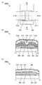
- the schematic diagram of the film-forming using a sputtering target and the said sputtering target The flowchart of a sputtering target preparation method.
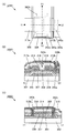
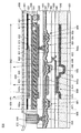
- 8A and 8B are a top view and cross-sectional views illustrating a semiconductor device.
- 8A and 8B are a top view and cross-sectional views illustrating a semiconductor device.
- FIG. 10 is a cross-sectional view illustrating a semiconductor device.
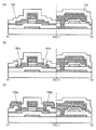
- FIG. 10 is a cross-sectional view illustrating a method for manufacturing a semiconductor device.
- 10 is a cross-sectional view illustrating a method for manufacturing a semiconductor device.
- 10 is a cross-sectional view illustrating a method for manufacturing a semiconductor device.
- 8A and 8B are a top view and cross-sectional views illustrating a semiconductor device.
- 8A and 8B are a top view and cross-sectional views illustrating a semiconductor device.
- 8A and 8B are a top view and cross-sectional views illustrating a semiconductor device.
- 8A and 8B are a top view and cross-sectional views illustrating a semiconductor device.
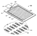
- FIG. 14 is a schematic perspective view illustrating a display device. Sectional drawing explaining a display apparatus.
- FIG. 10 is a schematic diagram illustrating an electronic device.
- a transistor is an element having at least three terminals including a gate, a drain, and a source.
- a channel region is provided between the drain (drain terminal, drain region or drain electrode) and the source (source terminal, source region or source electrode), and a current flows between the source and drain via the channel region.
- a channel region refers to a region through which a current mainly flows.
- the functions of the source and drain may be switched when transistors with different polarities are used or when the direction of current changes during circuit operation. Therefore, in this specification and the like, the terms source and drain can be used interchangeably.
- “electrically connected” includes a case of being connected via “something having an electric action”.
- the “thing having some electric action” is not particularly limited as long as it can exchange electric signals between connection targets.
- “thing having some electric action” includes electrodes, wiring, switching elements such as transistors, resistance elements, inductors, capacitors, and other elements having various functions.
- a silicon oxynitride film refers to a film having a higher oxygen content than nitrogen as the composition, and a silicon nitride oxide film has a nitrogen content as compared to oxygen as a composition. Refers to membranes with a lot of
- parallel means a state in which two straight lines are arranged at an angle of ⁇ 10 ° to 10 °. Therefore, the case of ⁇ 5 ° to 5 ° is also included.
- substantially parallel means a state in which two straight lines are arranged at an angle of ⁇ 30 ° to 30 °.
- Vertical refers to a state in which two straight lines are arranged at an angle of 80 ° to 100 °. Therefore, the case of 85 ° to 95 ° is also included.
- substantially vertical means a state in which two straight lines are arranged at an angle of 60 ° to 120 °.
- the terms “film” and “layer” can be interchanged with each other depending on circumstances.
- the term “conductive layer” may be changed to the term “conductive film”.
- the term “insulating film” may be changed to the term “insulating layer” in some cases.
- the semiconductor device may have characteristics as an “insulator”.
- the boundary between “semiconductor” and “insulator” is ambiguous and may not be strictly discriminated. Therefore, a “semiconductor” in this specification can be called an “insulator” in some cases.
- an “insulator” in this specification can be called a “semiconductor” in some cases.
- a metal oxide is a metal oxide in a broad expression.
- Metal oxides are classified into oxide insulators, oxide conductors (including transparent oxide conductors), oxide semiconductors (also referred to as oxide semiconductors or simply OS), and the like.
- oxide semiconductors also referred to as oxide semiconductors or simply OS
- the metal oxide may be referred to as an oxide semiconductor. That is, in the case of describing as an OS FET, it can be said to be a transistor including a metal oxide or an oxide semiconductor.
- the metal oxide described in this embodiment preferably contains at least indium. In particular, it is preferable to contain indium and zinc.
- element M element M is Al, Si, B, Y, Ti, Fe, Ni, Ge, Zr, Mo, La, Ce, Nd, Hf, Ta, W, Mg, V, Any one or a plurality of Be or Cu is included.
- the metal oxide includes indium, element M, and zinc.
- the terms of the atomic ratio of indium, element M, and zinc of the metal oxide are [In], [M], and [Zn].
- the metal oxide of one embodiment of the present invention preferably contains nitrogen.
- the nitrogen concentration obtained by SIMS is 1 ⁇ 10 16 atoms / cm 3 or more, preferably 1 ⁇ 10 17 atoms / cm 3 or more.
- the nitrogen concentration obtained by SIMS may be 2 ⁇ 10 22 atoms / cm 3 or less.
- FIG. 1A is a cross-sectional view of a sputtering target 10 for forming a metal oxide film by a sputtering method.
- FIG. 1B shows a state in which a metal oxide film is formed using the sputtering target 10.
- the sputtering target 10 has a first region 11 containing an insulating material (also referred to as a dielectric material) and a second region 12 containing a conductive material.
- the first region 11 and the second region 12 are separated from each other.
- the first region 11 has a higher resistance than the second region.
- the sputtering target 10 is functionally separated into the first region 11 that functions as an insulating region (also referred to as a dielectric region) and the second region 12 that functions as a conductive region. Yes.
- the sputtering target 10 has two phases having different properties: a first region 11 that functions as an insulating region and a second region 12 that functions as a conductive region. From this, the sputtering target 10 can be called a composite target.
- the first region 11 and the second region 12 are each preferably in the form of particles.
- Each of the first region 11 and the second region 12 preferably has a diameter of less than 10 ⁇ m.
- the sputtering target 10 may partially have a crystal structure.
- it may have a microcrystalline structure (sometimes referred to as an nc (nano-crystal) structure) or a polycrystalline structure.
- the diameter is preferably 0.5 nm to 3 nm, or 1 nm to 2 nm, or a value close thereto.
- the first region 11 includes the element M (the elements M are Al, Si, B, Y, Ti, Fe, Ni, Ge, Zr, Mo, La, Ce, Nd, Hf, Ta, W, Mg, V, Be, or Cu is preferably included, and the second region 12 preferably includes indium, zinc, or the like.
- the first region 11 and the second region 12 may include oxygen and / or nitrogen.
- the first region 11 may include an oxide, nitride, and / or oxynitride of the element M.
- the second region 12 may include an oxide such as indium or zinc, a nitride, and / or an oxynitride.
- the sputtering target 10 is functionally separated into an insulating region and a conductive region, it is preferable that the element M included in the first region 11 and the indium included in the second region do not combine.
- Examples of the insulating material included in the first region 11 include AlO x (x is a real number greater than 0), AlN y (y is a real number greater than 0), AlO x N y , BO x , SiO x , It is preferable to use one or more of SiN y and SiO x N y .
- the amount of oxygen or nitrogen in the oxide or nitride is typically 110% or less of the amount of oxygen or nitrogen having a stoichiometric composition.
- AlO x has a stoichiometric composition of Al 2 O 3 , typically 0 ⁇ x ⁇ 1.65.
- AlN y has a stoichiometric composition of AlN, typically 0 ⁇ y ⁇ 1.1.
- AlO x N y typically, 0 ⁇ x ⁇ 1.65 and 0 ⁇ y ⁇ 1.65.
- BO x has a stoichiometric composition of B 2 O 3 , typically 0 ⁇ x ⁇ 1.65.
- SiO x has a stoichiometric composition of SiO 2 , typically 0 ⁇ x ⁇ 2.2.
- SiN y has a stoichiometric composition of Si 3 N 4 , typically 0 ⁇ y ⁇ 1.47.
- SiO x N y typically, 0 ⁇ x ⁇ 2.2 and 0 ⁇ y ⁇ 2.2.
- Examples of the conductive material included in the second region 12 include InO x (x is a real number greater than 0), InN y (y is a real number greater than 0), InO x N y , ZnO x , ZnN y , and ZnO. x N y, or it is preferable to use any one InZn x O y, or more. Similar to the first region 11, the amount of oxygen or nitrogen in the oxide or nitride is typically 110% or less of the amount of oxygen or nitrogen in the stoichiometric composition.
- InO x has a stoichiometric composition of In 2 O 3 , typically 0 ⁇ x ⁇ 1.65.
- InN y has a stoichiometric composition of InN, typically 0 ⁇ y ⁇ 1.1.
- InO x N y typically, 0 ⁇ x ⁇ 1.65 and 0 ⁇ y ⁇ 1.65.
- ZnO x has a stoichiometric composition of ZnO, typically 0 ⁇ x ⁇ 1.1.
- ZnN y has a stoichiometric composition of Zn 3 N 2 , typically 0 ⁇ y ⁇ 0.73.
- In ZnO x N y typically, 0 ⁇ x ⁇ 1.1 and 0 ⁇ y ⁇ 1.1.
- the InZn x O y typically a 0 ⁇ x ⁇ 1.65,0 ⁇ y ⁇ 1.65.
- the metal oxide formed from the sputtering target 10 contains more conductive material than insulating material, carrier mobility can be further increased.
- the atomic ratio of indium contained in the conductive material contained in the sputtering target 10 is larger than the atomic ratio of element M contained in the insulating material.
- the composition of the sputtering target 10 is not limited to this, and may be appropriately set so as to satisfy, for example, the atomic ratio in the phase diagram shown in FIG.
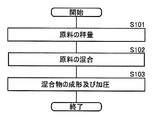
- the raw material for the conductive material and the raw material for the insulating material are weighed (step S101).
- the raw material of the conductive material for example, powdery indium oxide, indium nitride, indium oxynitride, zinc oxide, zinc nitride, and / or zinc oxynitride can be used.
- a raw material of the insulating material for example, powdered aluminum oxide, aluminum nitride, aluminum oxynitride, boron oxide, silicon oxide, silicon nitride, and / or silicon oxynitride are used. be able to.
- the raw material of the insulating material is not limited thereto, and for example, a powdered oxide, nitride, oxynitride, or the like of the element M may be used as appropriate.
- the alkali metal can be less than 10 ppm by weight, preferably less than 5 ppm by weight, and more preferably less than 2 ppm by weight.
- the alkaline earth metal can be less than 5 ppm by weight, preferably less than 2 ppm by weight, and more preferably less than 1 ppm by weight.
- each halogen can be less than 10 ppm by weight, preferably less than 5 ppm by weight, and more preferably less than 2 ppm by weight.
- impurity concentrations are determined by secondary ion mass spectrometry (SIMS), glow discharge mass spectrometry (GDMS), or inductively coupled plasma mass spectrometry (ICP-MS). (Plasma Mass Spectrometry) may be used.
- SIMS secondary ion mass spectrometry
- GDMS glow discharge mass spectrometry
- ICP-MS inductively coupled plasma mass spectrometry
- step S102 the weighed conductive material and insulating material are mixed to produce a mixture.
- a mixture of a conductive material and an insulating material is spread over a mold and molded (step S103).
- a press device or the like By pressing the mixture spread on the shaping mold using a press device or the like, it can be formed into a molded body.
- the conductive material (for example, indium or the like) and the insulating material (for example, indium or the like) and the insulating material (for example, indium or the like) can be obtained by producing a molded body only by pressing without using high-temperature heat treatment such as firing. , Element M, etc.) can be prevented from combining.
- the first region 11 that functions as an insulating region and the second region 12 that functions as a conductive region can be provided separately from each other in the sputtering target 10.
- the sputtering target 10 is produced by performing a finishing process with respect to the produced molded object. Specifically, in order to adjust the length, width, and thickness of the molded body, it is divided or ground. In addition, since the surface has minute irregularities, abnormal discharge may occur, so the surface is polished.
- the polishing treatment is preferably performed by CMP.
- step S102 when mixing the raw material of an electroconductive material and the raw material of an insulating material in step S102, you may mix water and organic substance (a dispersing agent and a binder), and you may make it a slurry. By slurrying and mixing the raw materials, the diameters of the first region 11 and the second region 12 included in the sputtering target 10 can be further reduced.
- water and organic substance a dispersing agent and a binder
- one or a plurality of suction ports are provided at the bottom of the molding die into which the slurry is poured when molding in step S103 so that water or the like can be sucked.
- a filter is provided at the bottom of the mold so that water and organic matter are allowed to pass through without passing the raw material powder.
- a filter in which a porous resin film is attached on a woven fabric or felt may be used.
- Step S103 water or the like is sucked from the slurry through a filter provided at the bottom of the mold, and the molded body is formed by removing water and organic substances from the slurry.
- the drying process is performed by natural drying because the molded body is difficult to crack.
- the flowchart shown in FIG. 3A differs from the flowchart shown in FIG. 2 in that a step of firing the molded body at a low temperature (step S104) is performed after step S103.
- a furnace also referred to as a firing furnace or a sintering furnace
- Firing may be performed in an atmosphere containing one or more of a rare gas, a nitrogen gas, and an oxygen gas.
- the firing may be performed in a nitrogen gas atmosphere.
- the temperature at which the molded body is fired is different from the raw material because the conductive material (for example, indium and the like) and the insulating material (for example, the element M and the like) do not combine with each other, for example, by heat. It is preferable that the temperature does not change to a compound. For example, it is preferable that the temperature for firing the compact is 200 ° C. or higher and lower than 1000 ° C.
- the strength of the sputtering target 10 can be further improved by firing the molded body at a low temperature to produce the sputtering target 10.
- the conductive material for example, indium
- the insulating material for example, indium
- an alloy 13 containing the element M or the like may be formed.
- the sputtering target 10 is produced by slurrying the mixture as described above, water and organic matter slightly remaining in the molded body can be removed by performing firing at a low temperature.
- step S103 for performing molding and pressurization and step S104 for performing low-temperature firing are separate processes, but the method described in this embodiment is limited to this. is not. For example, it is good also as a structure which pressurizes with a press apparatus, putting a mixture into a shaping
- FIG. 4A is a cross-sectional view illustrating the film formation chamber 41 included in the sputtering apparatus
- FIG. 4B is a plan view of the magnet unit 54a and the magnet unit 54b included in the sputtering apparatus.
- the 4A includes a target holder 52a, a target holder 52b, a backing plate 50a, a backing plate 50b, a sputtering target 10a, a sputtering target 10b, a member 58, and a substrate holder 62. And having.
- the sputtering target 10a is disposed on the backing plate 50a.
- the backing plate 50a is disposed on the target holder 52a.
- the magnet unit 54a is arrange
- the sputtering target 10b is arrange
- the backing plate 50b is disposed on the target holder 52b.
- the magnet unit 54b is arrange
- the magnet unit 54a includes a magnet 54N1, a magnet 54N2, a magnet 54S, and a magnet holder 56.
- the magnet 54N1, the magnet 54N2, and the magnet 54S are disposed on the magnet holder 56.
- the magnet 54N1 and the magnet 54N2 are disposed with a gap from the magnet 54S.
- the magnet unit 54b has the same structure as the magnet unit 54a.
- the sputtering target 10a, the backing plate 50a and the target holder 52a are separated from the sputtering target 10b, the backing plate 50b and the target holder 52b by a member 58.
- the member 58 is preferably an insulator.
- the member 58 may be a conductor or a semiconductor.
- the member 58 may be a conductor or semiconductor whose surface is covered with an insulator.
- the target holder 52a and the backing plate 50a are fixed using screws (bolts or the like) and are equipotential.
- the target holder 52a has a function of supporting the sputtering target 10a via the backing plate 50a.
- the target holder 52b and the backing plate 50b are fixed using screws (bolts or the like) and are equipotential.
- the target holder 52b has a function of supporting the sputtering target 10b through the backing plate 50b.
- the backing plate 50a has a function of fixing the sputtering target 10a.
- the backing plate 50b has a function of fixing the sputtering target 10b.
- FIG. 4A magnetic lines of force 64a and 64b formed by the magnet unit 54a are clearly shown.
- the magnet unit 54 a has a rectangular or substantially rectangular magnet 54 N 1, a rectangular or substantially rectangular magnet 54 N 2, and a rectangular or substantially rectangular magnet 54 S fixed to the magnet holder 56. It has the structure which is made. Then, the magnet unit 54a can be swung left and right as shown by the arrows in FIG. For example, the magnet unit 54a may be swung with a beat of 0.1 Hz to 1 kHz (in other words, rhythm, time signature, pulse, frequency, period, or cycle).
- the magnetic field on the sputtering target 10a changes as the magnet unit 54a swings. Since the region with a strong magnetic field is a high-density plasma region, the sputtering phenomenon of the sputtering target 10a tends to occur in the vicinity thereof. The same applies to the magnet unit 54b.
- FIG. 4 illustrates an example in which a facing target sputtering apparatus is used
- the metal oxide film forming method according to this embodiment is not limited thereto.
- the metal oxide may be formed using a parallel plate type sputtering apparatus.
- the first step includes a step of placing the substrate in the film formation chamber.
- the substrate 60 is placed on the substrate holder 62 included in the film forming chamber 41 shown in FIG.
- the temperature of the substrate 60 during film formation affects the electrical properties of the metal oxide.
- the higher the substrate temperature the higher the crystallinity of the metal oxide and the higher the reliability.
- the lower the substrate temperature the lower the crystallinity of the metal oxide and the higher the carrier mobility.
- the lower the substrate temperature at the time of film formation the more remarkable the field-effect mobility at a low gate voltage (for example, greater than 0 V and 2 V or less) in a transistor including a metal oxide.
- the temperature of the substrate 60 may be room temperature (25 ° C.) or higher and 150 ° C. or lower, preferably room temperature or higher and 130 ° C. or lower.
- the substrate temperature may be room temperature (25 ° C.) or higher and 150 ° C. or lower, preferably room temperature or higher and 130 ° C. or lower.
- it is suitable when a large-area glass substrate (for example, the above-described eighth generation or tenth generation glass substrate) is used.
- a cooling mechanism or the like may be provided in the substrate holder 62 to cool the substrate 60.
- the temperature of the substrate 60 is set to 100 ° C. or higher and 130 ° C. or lower, water in the metal oxide can be removed.
- water which is an impurity it is possible to improve the reliability while improving the field effect mobility.
- the productivity of the semiconductor device can be improved. Therefore, since the productivity is stable, it is easy to introduce a large-scale production apparatus, and thus a large display device using a large-area substrate can be easily manufactured.
- sDOS shallow defect levels
- the second step has a step of introducing gas into the film formation chamber.
- a gas is introduced into the film forming chamber 41 shown in FIG.
- the gas one or more of argon gas, oxygen gas, nitrogen gas, and hydrogen gas may be introduced.
- an inert gas such as helium, xenon, or krypton may be used instead of the argon gas.
- the carrier mobility of the metal oxide can be increased as the oxygen flow rate ratio is smaller.
- the field effect mobility is significantly improved at a low gate voltage (for example, a range of greater than 0 V and less than or equal to 2 V) in a transistor including a metal oxide.
- the oxygen flow rate ratio can be appropriately set within a range of 0% to 30% in order to obtain preferable characteristics according to the use of the metal oxide.
- the film forming gas can be a mixed gas of argon gas and oxygen gas. Further, by including oxygen gas in the deposition gas, the amount of oxygen vacancies in the deposited metal oxide can be reduced. Thus, by reducing the amount of oxygen vacancies, the reliability of the metal oxide can be improved.
- the oxygen flow rate ratio during metal oxide film formation is 0% to 30%, preferably 5% to 20%.
- a metal oxide containing nitrogen can be formed even when the sputtering target 10 does not contain nitrogen.
- the carrier mobility can be increased by increasing the nitrogen flow rate ratio and adding a sufficient amount of nitrogen to the metal oxide containing nitrogen. it can.
- field effect mobility can be improved at a low gate voltage (for example, in a range of greater than 0 V and less than or equal to 2 V) in a transistor including the metal oxide containing nitrogen. Become prominent.
- the nitrogen flow rate ratio can be appropriately set within a range of 10% or more and 100% or less in order to obtain preferable characteristics according to the use of the metal oxide having nitrogen.
- the film forming gas can be a mixed gas of nitrogen gas and argon gas.
- the film forming gas may be a mixed gas of nitrogen gas and oxygen gas, or a mixed gas of nitrogen gas, oxygen gas, and argon gas.
- nitrogen gas is included in the deposition gas, so that sites corresponding to oxygen vacancies in the metal oxide having nitrogen to be deposited are filled with nitrogen, and the amount of oxygen vacancies in the metal oxide having nitrogen is reduced. be able to.
- an element for example, silicon, aluminum, or the like
- a site corresponding to an oxygen deficiency of a metal oxide having nitrogen is determined as the element. Can be compensated by M.
- oxygen vacancies in the metal oxide containing nitrogen can be reduced even when oxygen in the deposition gas is reduced or even when the deposition gas does not contain oxygen.
- the carrier mobility of the metal oxide containing nitrogen can be improved by reducing the amount of oxygen in the metal oxide containing nitrogen and increasing the amount of nitrogen.
- oxygen gas when oxygen gas is used as a deposition gas during sputtering, the oxygen gas may be negatively ionized and collide with the metal oxide being deposited, which may damage the metal oxide.
- oxygen in the deposition gas is reduced or the deposition gas does not contain oxygen, whereby damage to the metal oxide can be prevented.
- nitrogen can be used as a film forming gas.
- the larger the hydrogen flow rate ratio the higher the carrier mobility of the metal oxide.
- the field effect mobility at a low gate voltage becomes more significant in a transistor including the metal oxide.
- oxygen gas, nitrogen gas, and argon gas used as a sputtering gas have a high purity up to a dew point of ⁇ 40 ° C. or lower, preferably ⁇ 80 ° C. or lower, more preferably ⁇ 100 ° C. or lower, more preferably ⁇ 120 ° C. or lower.
- the chamber in the sputtering apparatus is subjected to high vacuum (5 ⁇ 10 ⁇ 7 Pa to 1 ⁇ 10 ⁇ 4 Pa using an adsorption-type vacuum exhaust pump such as a cryopump. It is preferable to evacuate. Alternatively, it is preferable to combine a turbo molecular pump and a cold trap so that gas does not flow backward from the exhaust system into the chamber.
- the third step includes a step of applying a voltage to the sputtering target 10.
- a voltage is applied to the target holder 52a and the target holder 52b shown in FIG.
- the potential applied to the terminal V1 connected to the target holder 52a is set lower than the potential applied to the terminal V2 connected to the substrate holder 62.
- the potential applied to the terminal V4 connected to the target holder 52b is set lower than the terminal V2 connected to the substrate holder 62.
- the potential applied to the terminal V2 connected to the substrate holder 62 is set to the ground potential.
- the potential applied to the terminal V3 connected to the magnet holder 56 is set as the ground potential.
- the potential applied to the terminal V1, the terminal V2, the terminal V3, and the terminal V4 is not limited to the above-described potential. Further, the potential may not be applied to all of the target holder 52, the substrate holder 62, and the magnet holder 56. For example, the substrate holder 62 may be in an electrically floating state.
- a power source capable of controlling the applied potential is electrically connected to the terminal V1. As a power source, a DC power source, an AC power source, or an RF power source may be used.
- the fourth step includes a step of depositing a metal oxide from the sputtering target 10 onto the substrate.
- argon gas, nitrogen gas or oxygen gas is ionized in the film forming chamber 41 shown in FIG. 4, and plasma is formed by being divided into cations and electrons. Thereafter, positive ions in the plasma are accelerated toward the sputtering targets 10a and 10b by the potential applied to the target holders 52a and 52b. When the positive ions collide with the sputtering targets 10 a and 10 b, sputtered particles are generated, and the sputtered particles are deposited on the substrate 60.
- FIG. 1B shows a sputtering target 10, plasma 30, positive ions 20, first sputtered particles 11a, and second sputtered particles 12a.
- argon gas, oxygen gas or nitrogen gas is ionized to divide into cations 20 and electrons (not shown) to form plasma 30. Thereafter, the positive ions 20 in the plasma 30 are accelerated toward the sputtering target 10.
- the cations 20 collide with the sputtering target 10 the first sputtered particles 11a and the second sputtered particles 12a are generated, and the first sputtered particles 11a and the second sputtered particles 12a are ejected from the sputter target 10. It is.
- first sputtered particles 11a are ejected from the first region 11
- a cluster containing a large amount of the element M for example, aluminum, silicon, boron, or the like
- the second sputtered particles 12a are ejected from the second region 12
- a cluster containing a large amount of indium, zinc, or the like may be formed.
- the first sputtered particles 11a jumping out of the first region 11 containing the insulating material and the second sputtered particles 12a jumping out of the second region 12 containing the conductive material jump out onto the substrate. accumulate. On the substrate, an insulating region containing the first sputtered particles 11a and a conductive region containing the second sputtered particles 12a are formed unevenly.
- the metal oxide film formed using the sputtering target 10 has a conductive region and an insulating region which are separated from each other, and thus can also be referred to as a composite metal oxide.
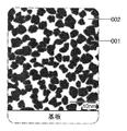
- the metal oxide according to one embodiment of the present invention includes the first region 001 containing each element as a main component and the second A region 002 is formed, and each region is mixed and formed in a mosaic shape.
- the metal oxide formed using the sputtering target 10 includes a first region 001 that functions as an insulating region and a second region 002 that functions as a conductive region.
- the first region 001 is a region mainly composed of the first sputtered particles 11a
- the second region 002 is a region mainly composed of the second sputtered particles 12a.
- a metal oxide one or more elements are unevenly distributed, and a region having the element has a size of 0.5 nm to 10 nm, preferably 0.5 nm to 3 nm, or a size in the vicinity thereof.
- the state mixed with is also referred to as a mosaic or patch.
- the first region 001 and the second region 002 included in the metal oxide are formed of the first sputtered particle 11a and the second sputtered particle 12a, and the first region 11 included in the sputtering target 10 and It becomes significantly smaller than the second region 12.
- the substrate temperature during film formation to room temperature (25 ° C.) to 150 ° C., preferably from room temperature to 130 ° C.
- particles deposited on the substrate are combined more than necessary by heat. Can be prevented.
- the size of the 1st field 001 and the 2nd field 002 can be made small as mentioned above.
- the physical characteristics of the first region 001 and the second region 002 are determined by the unevenly distributed elements. For example, when an element unevenly distributed in the first region 001 is compared with an element unevenly distributed in the second region 002, the element unevenly distributed in the first region 001 tends to be an insulator.
- the region 001 has a function of an insulator (dielectric) and becomes an insulator region.
- the second region 002 has a function of a conductor and serves as a conductor region.
- the material may function as a semiconductor.
- the metal oxide in one embodiment of the present invention is a kind of matrix composite or metal matrix composite in which materials having different physical characteristics are mixed.
- the metal oxide which is one embodiment of the present invention is a mixture of a region having a function of a conductor and a region having a function of an insulator, and the whole material functions as a semiconductor.
- it is defined as CAC (Cloud-Aligned Composite) -OS (Oxide Semiconductor) or CAC-metal oxide.
- the conductor region and the insulator region may be separated at the nanoparticle level. Further, in the material, the conductor region and the insulator region are unevenly distributed, and the periphery of the conductor region may be blurred and observed in a cloud shape. Note that in the CAC-OS or the CAC-metal oxide, the conductor region and the insulator region are each dispersed in the material with a size of 0.5 nm to 10 nm, preferably 0.5 nm to 3 nm. Is preferred.
- the size of the insulator region or the conductor region can be evaluated by EDX mapping obtained using energy dispersive X-ray spectroscopy (EDX: Energy Dispersive X-ray spectroscopy).
- the insulator region may be observed when the diameter of the insulator region is 0.5 nm or more and 10 nm or less, or 1 nm or more and 2 nm or less in EDX mapping of a cross-sectional photograph.
- the density of the main component element gradually decreases from the center to the periphery of the region.
- the peripheral portion of the region is unclear (blurred) in the EDX mapping of the cross-sectional photograph. Observed in state.
- the CAC-OS or the CAC-metal oxide does not include a stacked structure of two or more kinds of films having different compositions.
- a structure composed of two layers of a film mainly containing In and a film mainly containing element M is not included.
- CAC is an example of a function or a material structure
- the crystal structure is a secondary element in the CAC-OS or the CAC-metal oxide.
- CAAC c-axis aligned crystal
- the CAAC structure is a layered crystal structure in which a plurality of nanocrystals of IGZO have a c-axis orientation and are connected without being oriented in the ab plane.
- IGZO is a common name and sometimes refers to one compound of In, Ga, Zn, and O.
- a crystalline compound may be mentioned.
- the crystalline compound has a single crystal structure, a polycrystalline structure, or a CAAC structure.
- crystallinity in CAC-OS or CAC-metal oxide can be evaluated by electron diffraction.
- the electron diffraction pattern image a region having a high luminance in a ring shape is observed.
- a plurality of spots may be observed in the ring-shaped region.
- the conductor region When CAC-OS or CAC-metal oxide is used for an active layer of a transistor, the conductor region has a function of flowing electrons (or holes) serving as carriers, and the insulator (or dielectric) region is a carrier. It has a function not to flow electrons.
- the function of switching by switching the function as a conductor and the function as an insulator (on / off function) can be imparted to CAC-OS or CAC-metal oxide, respectively.
- CAC-OS or CAC-metal oxide by separating each function, both functions can be maximized.
- a metal oxide (hereinafter simply referred to as a metal oxide) containing indium, an element M, and zinc, which is a CAC-OS or a CAC-metal oxide, will be described.
- the terms of the atomic ratio of indium, element M, and zinc of the metal oxide are [In], [M], and [Zn].
- the metal oxide is indium oxide (hereinafter, InO X1 (X1 is a real number greater than 0)) or indium zinc oxide (hereinafter, In X2 Zn Y2 O Z2 (X2, Y2, and Z2).
- InO X1 X1 is a real number greater than 0
- In X2 Zn Y2 O Z2 X2, Y2, and Z2
- MO X3 X3 is a real number greater than 0
- M X4 Zn element M zinc oxide
- Y4 O Z4 (X4, Y4, and Z4 are real numbers greater than 0)) and the like, and the mosaic is formed by separating the material, and the mosaic InO X1 or In X2 Zn Y2 O Z2 It has a configuration distributed in the film (hereinafter also referred to as a cloud shape).
- the concept illustrated in FIG. 5 is the metal oxide of one embodiment of the present invention.
- the first region 001 is a region containing MO X3 as a main component
- the second region 002 is a region containing In X2 Zn Y2 O Z2 or InO X1 as a main component.
- the region where MO X3 is the main component and the region where In X2 Zn Y2 O Z2 or InO X1 is the main component are unclear (blurred), so there is a clear boundary between them. May not be observable.
- the number of atoms of the element M gradually decreases from the central portion to the peripheral portion, and instead, the number of Zn atoms increases, so that M X4 Zn Y4 O Z4 is the main. It gradually changes to the component area. Therefore, in EDX mapping, the periphery of the region where MO X3 is the main component is observed in an unclear (blurred) state.
- the metal oxide of one embodiment of the present invention is a metal oxide in which a region where MO X3 is a main component and a region where In X2 Zn Y2 O Z2 or InO X1 is a main component are mixed. is there.
- the second region 002 indicates that the In atomic ratio of the element M in the second region 002 is larger than the In atomic ratio of the element M in the first region 001. It is assumed that 002 has a higher In concentration than the first region 001.
- a region containing In X2 Zn Y2 O Z2 or InO X1 as a main component is a region having higher conductivity than a region containing MO X3 or the like as a main component. That, In X2 Zn Y2 O Z2 or InO X1, is an area which is the main component, by carriers flow, expressed the conductivity of the oxide semiconductor. Accordingly, a region where In X2 Zn Y2 O Z2 or InO X1 is a main component is distributed in a cloud shape in the oxide semiconductor, whereby high field-effect mobility ( ⁇ ) can be realized.
- areas such as MO X3 is the main component, as compared to the In X2 Zn Y2 O Z2 or InO X1 is the main component area, it is highly regions insulating. That is, the region whose main component is MO X3 or the like is distributed in the oxide semiconductor, whereby leakage current can be suppressed and a favorable switching operation can be realized.
- the metal oxide of one embodiment of the present invention is used for a semiconductor element
- the insulating property caused by MO X3 and the like and the conductivity caused by In X2 Zn Y2 O Z2 or InO X1 are complementary.
- a high on-current (I on ), a high field-effect mobility ( ⁇ ), and a low off-current (I off ) can be realized.
- the metal oxide of one embodiment of the present invention when nitrogen is added to the metal oxide of one embodiment of the present invention, the metal oxide tends to have a narrow band gap. Accordingly, it is possible to further increase the conductivity of the region mainly composed of In X2 Zn Y2 O Z2 or InO X1 . In other words, when a metal oxide to which nitrogen is added is used for a transistor, a transistor having higher on-state current (I on ) and higher field-effect mobility ( ⁇ ) can be obtained.
- I on on-state current
- ⁇ field-effect mobility
- the nitrogen concentration obtained by SIMS may be the numerical value described above.
- the metal oxide preferably has a high carrier density. Hydrogen contained in a metal oxide may combine with oxygen bonded to a metal atom to generate electrons that are carriers. Therefore, hydrogen may be added to the metal oxide of one embodiment of the present invention. Specifically, in the metal oxide of one embodiment of the present invention, the hydrogen concentration obtained by SIMS is 1 ⁇ 10 18 atoms / cm 3 or more, preferably 1 ⁇ 10 19 atoms / cm 3 or more. In the metal oxide of one embodiment of the present invention, the hydrogen concentration obtained by SIMS is 2 ⁇ 10 22 atoms / cm 3 or less.
- an oxide is formed also in a region mainly composed of MO X3 and the like, similarly to a region mainly composed of In X2 Zn Y2 O Z2 or InO X1 .
- an element having a large band gap such as aluminum or silicon (for example, an element having a larger band gap than gallium) as the element M, a region having sufficient insulating properties can be obtained even when an oxide is formed. it can.
- the band gap of Al 2 O 3 is 8.6 eV, which is larger than the band gap of Ga 2 O 3 4.8 eV.
- the band gap of AlN is 6.3 eV, which is larger than the band gap of GaN, 3.5 eV. That is, it is considered that the second region 002 when aluminum is used as the element M has higher insulating properties than the second region 002 when gallium is used as the element M. Therefore, when an element having a large band gap, such as aluminum or silicon, is used as the element M, a leakage current can be further suppressed and a good switching operation can be realized.
- the site corresponding to the oxygen deficiency of the metal oxide can be compensated by the element M. Further, nitrogen added to the metal oxide can also fill sites corresponding to oxygen vacancies.
- boron that can be used as the element M has a larger binding energy with oxygen than indium and zinc.
- the bond energy of B-O is 809 kJ / mol, which is larger than the bond energy of In-O 346 kJ / mol and the bond energy of Zn-O 250 kJ / mol.
- the bond energy of B—O is larger than the bond energy of Zn—O contained in the In—Ga—Zn-based metal oxide, 374 kJ / mol. That is, the second region 002 in the case of using boron oxide can stabilize the bonding of oxygen in the film and has higher insulation than the second region 002 in the case of using gallium oxide. It is thought to have.
- the metal oxide of one embodiment of the present invention can realize a favorable switching operation.
- oxygen deficiency also referred to as Vo refers to a state in which oxygen present in a metal oxide diffuses or disappears.
- oxygen vacancies occur in the metal oxide, the electric conductivity of the metal oxide may be changed.
- oxygen vacancies can be reduced by repairing (compensating) part of the defects with oxygen or a different element. By reducing oxygen vacancies, degradation due to electrical bias stress or thermal stress, and degradation due to light can be suppressed.
- the transistor including the metal oxide of one embodiment of the present invention is most suitable for various semiconductor devices including a display.
- AlNx may be formed in the metal oxide. Since AlNx has high thermal conductivity, a power device that can withstand use in a high-temperature environment can be manufactured by using a metal oxide containing AlNx for a transistor.
- the element M for example, aluminum is preferably used.
- aluminum oxide, aluminum zinc oxide, or the like is included in addition to the above.
- the element M for example, silicon is preferably used.
- silicon is preferably used as the element M.
- In—Si—Zn oxide using silicon as the element M includes silicon oxide, silicon zinc oxide, or the like.
- the concentration of Si obtained by SIMS is preferably 5 ⁇ 10 18 atoms / cm 3 or more.
- the metal oxide of one embodiment of the present invention is used for a semiconductor element, conduction that achieves high on-state current (I on ), high field-effect mobility ( ⁇ ), and low off-state current (I off ).
- the mechanism can be estimated by a random resistance network model which is one of percolation theory.
- the electrical conduction in the oxide of one embodiment of the present invention is basically that an electron which is a carrier freely moves in a region where In X2 Zn Y2 O Z2 or InO X1 having high conductivity is a main component. This is thought to be caused by
- a semiconductor element using the metal oxide of one embodiment of the present invention has high reliability. Therefore, the metal oxide of one embodiment of the present invention is most suitable for various semiconductor devices including a display.
- FIG. 6 is a modification of the conceptual diagram shown in FIG. As shown in FIG. 6, in addition to the first region 001 and the second region 002, a third region 003 may be included.
- the third region 003 may be formed depending on metal oxide formation conditions. For example, as the third region 003, one compound of In, the elements M, Zn, and O may be formed. Further, the concentration of the element M is lower than that of the first region 001, the concentration of the element M is higher than that of the first region 001, and the concentration of In is lower than that of the second region 002. A region having a higher In concentration than the region 002 may be formed as the third region 003 in some cases.
- the third region 003 is a region having higher conductivity than the first region 001 and higher insulation than the second region 002. Therefore, basically, the third region 003 does not flow carriers and does not contribute to the switching operation. That is, it is an area that basically has no function.
- Embodiment 2 In this embodiment, a semiconductor device using the metal oxide described in Embodiment 1 and a method for manufacturing the semiconductor device will be described with reference to FIGS.
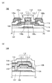
- FIG. 7A is a top view of the transistor 100 which is a semiconductor device of one embodiment of the present invention
- FIG. 7B is a cross-sectional view taken along the dashed-dotted line X1-X2 in FIG. 7C corresponds to a cross-sectional view of a cross-sectional surface taken along alternate long and short dash line Y1-Y2 in FIG. 7A.
- some components such as an insulating film functioning as a gate insulating film
- the direction of the alternate long and short dash line X1-X2 may be referred to as a channel length direction, and the direction of the alternate long and short dash line Y1-Y2 may be referred to as a channel width direction. Note that in the top view of the transistor, some components may be omitted in the following drawings as in FIG. 7A.
- 7A, 7B, and 7C is a so-called top-gate transistor.
- the transistor 100 includes an insulating film 104 over a substrate 102, a metal oxide film 108 over the insulating film 104, an insulating film 110 over the metal oxide film 108, a conductive film 112 over the insulating film 110, and an insulating film 104. And the metal oxide film 108 and the insulating film 116 over the conductive film 112.
- the metal oxide film 108 the metal oxide described in Embodiment 1 can be used.
- the metal oxide film 108 over the insulating film 104 has a channel formation region in a region where the conductive film 112 overlaps.
- the metal oxide film 108 includes In and M (M is Al, Si, B, Y, Ti, Fe, Ni, Ge, Zr, Mo, La, Ce, Nd, Hf, Ta, W, Mg, Any one or more of V, Be, or Cu) and Zn are preferable.
- the metal oxide film 108 has a region 108n in a region where the conductive film 112 is not overlapped and the insulating film 116 is in contact.
- the region 108n is a region in which the metal oxide film 108 described above is n-type. Note that the region 108n is in contact with the insulating film 116, and the insulating film 116 contains nitrogen or hydrogen. Therefore, when nitrogen or hydrogen in the insulating film 116 is added to the region 108n, the carrier density is increased and the region becomes n-type.
- the metal oxide film 108 preferably has a region where the atomic ratio of In is larger than the atomic ratio of M.
- the metal oxide film 108 is not limited to the above composition.
- M is 0.5 or more and 1.5 or less
- Zn is 5 or more and 7 or less.
- the field-effect mobility of the transistor 100 can be increased. Specifically, the field effect mobility of the transistor 100 can exceed 50 cm 2 / V s , and more preferably, the field effect mobility of the transistor 100 can exceed 100 cm 2 / V s .
- a display device with a narrow frame width (also referred to as a narrow frame) can be provided by using the above-described transistor with high field-effect mobility for a gate driver that generates a gate signal.
- the above transistor with high field-effect mobility is used for a source driver that supplies signals from a signal line included in a display device (particularly, a demultiplexer connected to an output terminal of a shift register included in the source driver).
- a display device with a small number of wirings connected to the display device can be provided.
- the metal oxide film 108 has a region where the atomic ratio of In is larger than the atomic ratio of M, when the crystallinity of the metal oxide film 108 is high, the field-effect mobility is low. There is a case.
- the crystallinity of the metal oxide film 108 is analyzed using, for example, X-ray diffraction (XRD: X-Ray Diffraction), or analyzed using a transmission electron microscope (TEM: Transmission Electron Microscope). Can be analyzed.
- XRD X-ray diffraction
- TEM Transmission Electron Microscope
- the transistor 100 includes a region 108n through an insulating film 118 over the insulating film 116 and an opening 141a provided in the insulating films 116 and 118.
- the conductive film 120a may be electrically connected to the region 108n and the conductive film 120b may be electrically connected to the region 108n through the opening 141b provided in the insulating films 116 and 118.
- the insulating film 104 is a first insulating film
- the insulating film 110 is a second insulating film
- the insulating film 116 is a third insulating film
- the insulating film 118 is a fourth insulating film.
- the conductive film 112 functions as a gate electrode
- the conductive film 120a functions as a source electrode
- the conductive film 120b functions as a drain electrode.
- the insulating film 110 functions as a gate insulating film.
- excess oxygen may be supplied to the insulating film 104 formed below the metal oxide film 108.
- excess oxygen contained in the insulating film 104 can be supplied also to the region 108n.
- excess oxygen is supplied into the region 108n, the resistance in the region 108n increases, which is not preferable.
- the insulating film 110 formed over the metal oxide film 108 has excess oxygen, it is possible to selectively supply excess oxygen only to a region overlapping with the conductive film 112. .
- the substrate 102 There is no particular limitation on the material of the substrate 102, but it is necessary that the substrate 102 have at least heat resistance to withstand heat treatment performed later.
- a glass substrate, a ceramic substrate, a quartz substrate, a sapphire substrate, or the like may be used as the substrate 102.
- a single crystal semiconductor substrate made of silicon or silicon carbide, a polycrystalline semiconductor substrate, a compound semiconductor substrate such as silicon germanium, an SOI substrate, or the like can be applied, and a semiconductor element is provided over these substrates.
- a substrate may be used as the substrate 102.
- the sixth generation (1500 mm ⁇ 1850 mm), the seventh generation (1870 mm ⁇ 2200 mm), the eighth generation (2200 mm ⁇ 2400 mm), the ninth generation (2400 mm ⁇ 2800 mm), the tenth generation.
- a large area substrate such as a generation (2950 mm ⁇ 3400 mm)
- a large display device can be manufactured.
- a flexible substrate may be used as the substrate 102, and the transistor 100 may be formed directly over the flexible substrate.
- a separation layer may be provided between the substrate 102 and the transistor 100. The separation layer can be used for separation from the substrate 102 and transfer to another substrate after the semiconductor device is partially or entirely completed thereon. At that time, the transistor 100 can be transferred to a substrate having poor heat resistance or a flexible substrate.
- the insulating film 104 can be formed using a sputtering method, a CVD method, an evaporation method, a pulsed laser deposition (PLD) method, a printing method, a coating method, or the like as appropriate.
- a sputtering method for example, an oxide insulating film or a nitride insulating film can be formed as a single layer or a stacked layer.
- at least a region in contact with the metal oxide film 108 in the insulating film 104 is preferably formed using an oxide insulating film. Further, by using an oxide insulating film from which oxygen is released by heating as the insulating film 104, oxygen contained in the insulating film 104 can be transferred to the metal oxide film 108 by heat treatment.
- the thickness of the insulating film 104 can be 50 nm or more, 100 nm or more and 3000 nm or less, or 200 nm or more and 1000 nm or less.
- the thickness of the insulating film 104 By increasing the thickness of the insulating film 104, the amount of oxygen released from the insulating film 104 can be increased, and the interface state at the interface between the insulating film 104 and the metal oxide film 108 and included in the metal oxide film 108. Oxygen deficiency can be reduced.
- the insulating film 104 for example, silicon oxide, silicon oxynitride, silicon nitride oxide, silicon nitride, aluminum oxide, hafnium oxide, gallium oxide, Ga—Zn oxide, or the like may be used, and the insulating film 104 can be provided as a single layer or a stacked layer.
- a stacked structure of a silicon nitride film and a silicon oxynitride film is used as the insulating film 104.
- oxygen can be efficiently introduced into the metal oxide film 108 by using the insulating film 104 as a stacked structure and using a silicon nitride film on the lower layer side and a silicon oxynitride film on the upper layer side.
- the conductive films 112, 120a, and 120b each include an oxide containing indium and tin (In—Sn oxide), an oxide containing indium and tungsten (In—W oxide), indium, tungsten, and zinc.
- a metal oxide such as (Zn oxide) or an oxide conductor can also be used.
- the oxide conductor will be described.
- the oxide conductor may be referred to as OC (Oxide Conductor).
- Oxide Conductor As an oxide conductor, for example, when an oxygen vacancy is formed in a metal oxide and hydrogen is added to the oxygen vacancy, a donor level is formed in the vicinity of the conduction band. As a result, the metal oxide becomes highly conductive and becomes a conductor.
- the conductive metal oxide can be referred to as an oxide conductor.
- a metal oxide has a large energy gap and thus has a light-transmitting property with respect to visible light.
- an oxide conductor is a metal oxide having a donor level near the conduction band. Therefore, the oxide conductor is less affected by the absorption due to the donor level and has a light-transmitting property similar to that of the metal oxide with respect to visible light.
- a Cu-X alloy film (X is Mn, Ni, Cr, Fe, Co, Mo, Ta, or Ti) may be applied to the conductive films 112, 120a, and 120b.
- X is Mn, Ni, Cr, Fe, Co, Mo, Ta, or Ti
- a Cu-X alloy film it can be processed by a wet etching process, and thus manufacturing costs can be suppressed.
- the conductive films 112, 120a, and 120b preferably include any one or more selected from titanium, tungsten, tantalum, and molybdenum among the above metal elements.
- a tantalum nitride film is preferably used as the conductive films 112, 120a, and 120b.
- the tantalum nitride film has conductivity and high barrier properties against copper or hydrogen. Further, since the tantalum nitride film emits less hydrogen from itself, the tantalum nitride film can be preferably used as a conductive film in contact with the metal oxide film 108 or a conductive film in the vicinity of the metal oxide film 108.
- the conductive films 112, 120a, and 120b can be formed by an electroless plating method.
- a material that can be formed by the electroless plating method for example, any one or more selected from Cu, Ni, Al, Au, Sn, Co, Ag, and Pd can be used.
- the use of Cu or Ag is preferable because the resistance of the conductive film can be lowered.
- a silicon oxide film, a silicon oxynitride film, a silicon nitride oxide film, or the like is formed by a plasma enhanced chemical vapor deposition (PECVD) method, a sputtering method, or the like. Insulation including one or more of films, silicon nitride films, aluminum oxide films, hafnium oxide films, yttrium oxide films, zirconium oxide films, gallium oxide films, tantalum oxide films, magnesium oxide films, lanthanum oxide films, cerium oxide films, and neodymium oxide films Layers can be used. Note that the insulating film 110 may have a two-layer structure or a three-layer structure.
- hafnium oxide when used as the insulating film 110, the following effects are obtained.
- Hafnium oxide has a higher dielectric constant than silicon oxide or silicon oxynitride. Therefore, since the thickness of the insulating film 110 can be increased as compared with the case where silicon oxide is used, the leakage current due to the tunnel current can be reduced. That is, a transistor with a small off-state current can be realized.
- hafnium oxide having a crystal structure has a higher dielectric constant than hafnium oxide having an amorphous structure. Therefore, in order to obtain a transistor with low off-state current, it is preferable to use hafnium oxide having a crystal structure. Examples of the crystal structure include a monoclinic system and a cubic system. Note that one embodiment of the present invention is not limited thereto.
- the insulating film 110 preferably has few defects. Typically, it is preferable that the number of signals observed by an electron spin resonance (ESR) be small.
- the signal described above includes the E ′ center where the g value is observed at 2.001.
- the E ′ center is caused by silicon dangling bonds.
- As the insulating film 110 a silicon oxide film or a silicon oxynitride film whose spin density due to the E ′ center is 3 ⁇ 10 17 spins / cm 3 or less, preferably 5 ⁇ 10 16 spins / cm 3 or less is used. Good.
- Metal oxide film As the metal oxide film 108, the metal oxide described in the above embodiment can be used.
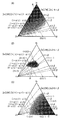
- FIGS. 17 (A), 17 (B), and 17 (C). a preferable range of the atomic ratio of indium, element M, and zinc included in the metal oxide according to the present invention will be described with reference to FIGS. 17 (A), 17 (B), and 17 (C). .
- FIG. 17A, FIG. 17B, and FIG. 17C do not describe the atomic ratio of oxygen and nitrogen.
- the terms of the atomic ratio of indium, element M, and zinc of the metal oxide are [In], [M], and [Zn].
- [In]: [M]: [Zn] (1 + ⁇ ): (1- ⁇ ): number of atoms of 4
- a line to be a ratio and a line to have an atomic ratio of [In]: [M]: [Zn] (1 + ⁇ ) :( 1 ⁇ ): 5.
- multiple phases may coexist in the metal oxide (two-phase coexistence, three-phase coexistence, etc.).
- two phases of a spinel crystal structure and a layered crystal structure tend to coexist.
- two phases of a bixbite type crystal structure and a layered crystal structure tend to coexist.
- a crystal grain boundary may be formed between different crystal structures.
- Region A shown in FIG. 17A shows an example of a preferable range of the atomic ratio of indium, element M, and zinc included in the metal oxide.
- the metal oxide can increase the carrier mobility (electron mobility) of the metal oxide by increasing the content of indium. Therefore, a metal oxide having a high indium content has higher carrier mobility than a metal oxide having a low indium content.
- the metal oxide of one embodiment of the present invention have an atomic ratio shown by a region A in FIG.
- the properties of metal oxides are not uniquely determined by the atomic ratio. Even if the atomic ratio is the same, the properties of the metal oxide may differ depending on the formation conditions. For example, when a metal oxide is formed using a sputtering apparatus, a film having an atomic ratio that deviates from the atomic ratio of the sputtering target is formed. Further, depending on the substrate temperature during film formation, [Zn] of the film may be smaller than [Zn] of the sputtering target. Therefore, the illustrated region is a region that exhibits an atomic ratio in which the metal oxide tends to have specific characteristics, and the boundaries of the regions A to C are not strict.
- the atomic ratio of the metal oxide film 108 to be formed includes a variation of plus or minus 40% of the atomic ratio of the metal element contained in the sputtering target.
- the metal oxide film 108 has an energy gap of 2 eV or more, preferably 2.5 eV, more preferably 3.0 eV or more. In this manner, off-state current of the transistor 100 can be reduced by using a metal oxide having a wide energy gap.
- the metal oxide film 108 preferably has a non-single crystal structure.
- the non-single-crystal structure includes, for example, a CAAC-OS, a polycrystalline structure, a microcrystalline structure, or an amorphous structure.
- the amorphous structure has the highest density of defect states.
- the insulating film 116 includes nitrogen or hydrogen.
- An example of the insulating film 116 is a nitride insulating film.
- the nitride insulating film can be formed using silicon nitride, silicon nitride oxide, silicon oxynitride, or the like.
- the concentration of hydrogen contained in the insulating film 116 is preferably 1 ⁇ 10 22 atoms / cm 3 or more.
- the insulating film 116 is in contact with the region 108n of the metal oxide film 108. Accordingly, the concentration of nitrogen or hydrogen in the region 108n in contact with the insulating film 116 is increased, and the carrier density in the region 108n can be increased.
- the metal oxide film 108 also includes nitrogen, adhesion between the insulating film 116 and the metal oxide film 108 can be improved.
- an oxide insulating film can be used.
- a stacked film of an oxide insulating film and a nitride insulating film can be used.
- the insulating film 118 for example, silicon oxide, silicon oxynitride, silicon nitride oxide, aluminum oxide, hafnium oxide, gallium oxide, Ga—Zn oxide, or the like may be used.
- the insulating film 118 is preferably a film that functions as a barrier film of hydrogen, water, etc. from the outside.
- the thickness of the insulating film 118 can be greater than or equal to 30 nm and less than or equal to 500 nm, or greater than or equal to 100 nm and less than or equal to 400 nm.
- FIG. 8A is a top view of the transistor 150
- FIG. 8B is a cross-sectional view along the dashed-dotted line X1-X2 in FIG. 8A
- FIG. 8C is FIG. 8A. It is sectional drawing between dashed-dotted lines Y1-Y2.
- 8A, 8B, and 8C includes a conductive film 106 over a substrate 102, an insulating film 104 over the conductive film 106, a metal oxide film 108 over the insulating film 104, and a metal oxide film.
- the insulating film 110 over the material film 108, the conductive film 112 over the insulating film 110, the insulating film 104, the metal oxide film 108, and the insulating film 116 over the conductive film 112 are included.
- the metal oxide film 108 has a structure similar to that of the transistor 100 illustrated in FIGS.
- a transistor 150 illustrated in FIGS. 8A, 8 ⁇ / b> B, and 8 ⁇ / b> C includes a conductive film 106 and an opening 143 in addition to the structure of the transistor 100 described above.
- the opening 143 is provided in the insulating films 104 and 110.
- the conductive film 106 is electrically connected to the conductive film 112 through the opening 143. Therefore, the same potential is applied to the conductive film 106 and the conductive film 112. Note that different potentials may be applied to the conductive film 106 and the conductive film 112 without providing the opening 143.
- the conductive film 106 may be used as a light-blocking film without providing the opening 143. For example, when the conductive film 106 is formed using a light-blocking material, light from below applied to the active layer of the metal oxide film 108 can be suppressed.
- the conductive film 106 functions as a first gate electrode (also referred to as a bottom gate electrode), and the conductive film 112 is also referred to as a second gate electrode (also referred to as a top gate electrode). ).
- the insulating film 104 has a function as a first gate insulating film, and the insulating film 110 has a function as a second gate insulating film.
- the conductive film 106 As the conductive film 106, the same material as the conductive films 112, 120a, and 120b described above can be used. In particular, the conductive film 106 is preferably formed using a material containing copper because the resistance can be lowered.
- the conductive film 106 has a stacked structure in which a copper film is provided over a titanium nitride film, a tantalum nitride film, or a tungsten film, and the conductive films 120a and 120b are provided with a copper film over the titanium nitride film, the tantalum nitride film, or the tungsten film. A laminated structure is preferable.
- the transistor 150 for one or both of the pixel transistor and the driving transistor of the display device, parasitic capacitance generated between the conductive film 106 and the conductive film 120a and the conductive film 106 and the conductive film 120b The parasitic capacitance generated between them can be reduced. Therefore, the conductive film 106, the conductive film 120a, and the conductive film 120b are used not only as the first gate electrode, the source electrode, and the drain electrode of the transistor 150, but also for power supply wiring and signal supply of the display device. It can also be used for wiring or wiring for connection.
- the transistor 150 illustrated in FIGS. 8A, 8B, and 8C has a structure in which conductive films functioning as gate electrodes are provided above and below the metal oxide film 108, unlike the transistor 100 described above.
- the semiconductor device of one embodiment of the present invention may include a plurality of gate electrodes.
- the metal oxide film 108 is opposite to the conductive film 106 functioning as the first gate electrode and the conductive film 112 functioning as the second gate electrode, respectively. And is sandwiched between conductive films functioning as two gate electrodes.
- the length of the conductive film 112 in the channel width direction is longer than the length of the metal oxide film 108 in the channel width direction, and the entire length of the metal oxide film 108 in the channel width direction is conductive with the insulating film 110 interposed therebetween.
- the film 112 is covered.
- the conductive film 112 and the conductive film 106 are connected to each other in the insulating film 104 and the opening 143 provided in the insulating film 110, one of the side surfaces in the channel width direction of the metal oxide film 108 is the insulating film 110. Is opposed to the conductive film 112.
- the conductive film 106 and the conductive film 112 are connected in the opening 143 provided in the insulating films 104 and 110 and have a region located outside the side end of the metal oxide film 108.
- the metal oxide film 108 included in the transistor 150 is electrically formed by an electric field of the conductive film 106 functioning as the first gate electrode and the conductive film 112 functioning as the second gate electrode. Can be surrounded.
- a device structure of a transistor that surrounds the metal oxide film 108 in which a channel region is formed by an electric field of the first gate electrode and the second gate electrode is a surround channel (S-channel) structure. Can be called.
- the transistor 150 Since the transistor 150 has an S-channel structure, an electric field for inducing a channel by the conductive film 106 or the conductive film 112 can be effectively applied to the metal oxide film 108; thus, the current driving capability of the transistor 150 Thus, high on-current characteristics can be obtained. Further, since the on-state current can be increased, the transistor 150 can be miniaturized. In addition, since the transistor 150 has a structure in which the metal oxide film 108 is surrounded by the conductive film 106 and the conductive film 112, the mechanical strength of the transistor 150 can be increased.
- an opening different from the opening 143 may be formed on the side where the opening 143 of the metal oxide film 108 is not formed in the channel width direction of the transistor 150.
- the signal A is supplied to one gate electrode and the fixed potential is supplied to the other gate electrode.
- Vb may be given.
- the signal A may be given to one gate electrode, and the signal B may be given to the other gate electrode.
- One gate electrode may be given a fixed potential Va, and the other gate electrode may be given a fixed potential Vb.
- the signal A is a signal for controlling, for example, a conduction state or a non-conduction state.
- the signal A may be a digital signal that takes two kinds of potentials, that is, the potential V1 or the potential V2 (V1> V2).
- the potential V1 can be a high power supply potential and the potential V2 can be a low power supply potential.
- the signal A may be an analog signal.
- the fixed potential Vb is a potential for controlling the threshold voltage VthA of the transistor, for example.
- the fixed potential Vb may be the potential V1 or the potential V2. In this case, it is preferable that a potential generating circuit for generating the fixed potential Vb does not need to be provided separately.
- the fixed potential Vb may be a potential different from the potential V1 or the potential V2.
- the threshold voltage VthA can be increased by lowering the fixed potential Vb. As a result, the drain current when the gate-source voltage Vgs is 0 V can be reduced, and the leakage current of a circuit including a transistor can be reduced in some cases.
- the fixed potential Vb may be set lower than the low power supply potential.
- the threshold voltage VthA can be lowered by increasing the fixed potential Vb.
- the drain current when the gate-source voltage Vgs is at a high power supply potential can be improved, and the operation speed of a circuit including a transistor can be improved in some cases.
- the fixed potential Vb may be higher than the low power supply potential.
- the signal B is a signal for controlling a conduction state or a non-conduction state, for example.
- the signal B may be a digital signal that takes two kinds of potentials, that is, the potential V3 or the potential V4 (V3> V4).
- the potential V3 can be a high power supply potential and the potential V4 can be a low power supply potential.
- the signal B may be an analog signal.
- the signal B may be a signal having the same digital value as the signal A.
- the on-state current of the transistor can be improved and the operation speed of the circuit including the transistor can be improved in some cases.
- the potential V1 and the potential V2 in the signal A may be different from the potential V3 and the potential V4 in the signal B.
- the potential amplitude (V3 to V4) of the signal B is It may be larger than the potential amplitude (V1-V2). By doing so, the influence of the signal A and the influence of the signal B on the conduction state or non-conduction state of the transistor may be approximately the same.
- the signal B may be a signal having a digital value different from that of the signal A.
- the transistor can be controlled separately by the signal A and the signal B, and a higher function may be realized.
- the transistor is an n-channel transistor
- the transistor A is in a conductive state only when the signal A is the potential V1 and the signal B is the potential V3, or the signal A is the potential V2 and the signal B is In the case where a non-conducting state is obtained only when the potential is V4, functions such as a NAND circuit and a NOR circuit may be realized with one transistor.
- the signal B may be a signal for controlling the threshold voltage VthA.
- the signal B may be a signal having a different potential between a period in which a circuit including a transistor is operating and a period in which the circuit is not operating.
- the signal B may be a signal having a different potential according to the operation mode of the circuit. In this case, the potential of the signal B may not be switched as frequently as the signal A.
- the signal B is an analog signal having the same potential as the signal A, an analog signal obtained by multiplying the potential of the signal A by a constant, or the potential of the signal A is added or subtracted by a constant.
- An analog signal or the like may be used.
- the on-state current of the transistor can be improved and the operation speed of the circuit including the transistor can be improved in some cases.
- the signal B may be an analog signal different from the signal A. In this case, the transistor can be controlled separately by the signal A and the signal B, and a higher function may be realized.
- the signal A may be a digital signal and the signal B may be an analog signal.
- the signal A may be an analog signal and the signal B may be a digital signal.
- the transistor When a fixed potential is applied to both gate electrodes of a transistor, the transistor may function as an element equivalent to a resistance element.
- the effective resistance of the transistor can be decreased (increased) by increasing (decreasing) the fixed potential Va or the fixed potential Vb in some cases.
- an effective resistance lower (higher) than that obtained by a transistor having only one gate may be obtained.
- a transistor 150 illustrated in FIGS. 8A, 8 ⁇ / b> B, and 8 ⁇ / b> C includes an insulating film 122 over the conductive films 120 a and 120 b and the insulating film 118.
- the insulating film 122 has a function of flattening unevenness caused by a transistor or the like.
- the insulating film 122 only needs to be insulative and is formed using an inorganic material or an organic material.
- the inorganic material include a silicon oxide film, a silicon oxynitride film, a silicon nitride oxide film, a silicon nitride film, an aluminum oxide film, and an aluminum nitride film.
- photosensitive resin materials such as an acrylic resin or a polyimide resin, are mentioned, for example.
- FIG. 9A and 9B are cross-sectional views of the transistor 160.
- 9A and 9B is different from the transistor 150 in the stacked structure of the conductive film 112, the shape of the conductive film 112, and the shape of the insulating film 110.
- the conductive film 112 of the transistor 160 includes a conductive film 112_1 over the insulating film 110 and a conductive film 112_2 over the conductive film 112_1.
- an oxide conductive film can be used as the conductive film 112_1.
- the oxide conductive film may be formed in an atmosphere containing oxygen gas by a sputtering method.
- the oxide conductive film for example, an oxide having indium and tin, an oxide having tungsten and indium, an oxide having tungsten, indium, and zinc, an oxide having titanium and indium, Examples thereof include an oxide having titanium, indium, and tin, an oxide having indium and zinc, an oxide having silicon, indium, and tin, and an oxide having indium, gallium, and zinc.
- the conductive film 112_2 and the conductive film 106 are connected to each other in the opening 143.
- the opening 143 is formed, after the conductive film to be the conductive film 112_1 is formed, the opening 143 is formed, whereby the shape illustrated in FIG. 9B can be obtained.
- the connection resistance between the conductive film 112 and the conductive film 106 can be reduced by connecting the conductive film 112_2 and the conductive film 106.
- the conductive film 112 and the insulating film 110 of the transistor 160 are tapered. More specifically, the lower end portion of the conductive film 112 is formed outside the upper end portion of the conductive film 112. The lower end portion of the insulating film 110 is formed outside the upper end portion of the insulating film 110. Further, the lower end portion of the conductive film 112 is formed at substantially the same position as the upper end portion of the insulating film 110.
- the tapered shape of the conductive film 112 and the insulating film 110 of the transistor 160 is preferable because the coverage of the insulating film 116 can be increased as compared to the case where the conductive film 112 and the insulating film 110 of the transistor 160 are rectangular. is there.
- transistor 160 Note that the other structure of the transistor 160 is similar to that of the transistor 150 described above, and has the same effect.
- FIGS. 8A to 8C are cross-sectional views in the channel length direction and the channel width direction, which illustrate a method for manufacturing the transistor 150.
- a conductive film 106 is formed on the substrate 102.
- the insulating film 104 is formed over the substrate 102 and the conductive film 106, and a metal oxide film is formed over the insulating film 104.
- the metal oxide film 108a is formed by processing the metal oxide film into an island shape (see FIG. 10A).
- the conductive film 106 can be formed by selecting the materials described above.
- a sputtering film is used as the conductive film 106, and a stacked film of a tungsten film with a thickness of 50 nm and a copper film with a thickness of 400 nm is formed.
- a method for processing the conductive film to be the conductive film 106 one or both of a wet etching method and a dry etching method may be used.
- the conductive film is processed by etching the tungsten film by a dry etching method, so that the conductive film 106 is formed.
- the insulating film 104 can be formed using a sputtering method, a CVD method, a vapor deposition method, a pulsed laser deposition (PLD) method, a printing method, a coating method, or the like as appropriate.
- a 400-nm-thick silicon nitride film and a 50-nm-thick silicon oxynitride film are formed as the insulating film 104 using a PECVD apparatus.
- an inert gas for example, helium gas, argon gas, xenon gas, etc.
- oxygen flow ratio the ratio of oxygen gas to the entire deposition gas in forming the metal oxide film 108a is 0% to 30%, preferably 5% to 20%. is there.
- the ratio of nitrogen gas in the entire film formation gas is such that the nitrogen gas in the entire film formation gas is 10% to 100%.
- nitrogen when nitrogen is included as a sputtering gas, nitrogen can be added to the metal oxide simultaneously with the formation of the metal oxide.
- the substrate temperature may be a room temperature to 150 ° C., preferably the substrate temperature may be a room temperature to 130 ° C.
- productivity is preferably increased.
- the thickness of the metal oxide film 108a may be 3 nm to 200 nm, preferably 3 nm to 100 nm, more preferably 3 nm to 60 nm.
- the substrate temperature when the metal oxide film 108a is formed is 200 ° C. or higher and 300 ° C. or lower. 102 may be deformed (distorted or warped). Therefore, in the case where a large glass substrate is used, deformation of the glass substrate can be suppressed by setting the substrate temperature at the time of forming the metal oxide film 108 a to be room temperature or higher and lower than 200 ° C.
- oxygen gas, nitrogen gas, and argon gas used as the sputtering gas have a high purity up to a dew point of ⁇ 40 ° C. or lower, preferably ⁇ 80 ° C. or lower, more preferably ⁇ 100 ° C. or lower, more preferably ⁇ 120 ° C. or lower.
- the chamber in the sputtering apparatus is subjected to a high vacuum (5 ⁇ 10 ⁇ 7 Pa to 1 ⁇ 10 ⁇ 4) using an adsorption-type vacuum exhaust pump such as a cryopump. It is preferable to exhaust to about Pa).
- the formation conditions of the metal oxide film 108a are as follows.
- the formation conditions of the metal oxide film 108a are formed by a sputtering method using a metal oxide target (composite target). Further, the substrate temperature, the oxygen flow rate ratio, and the nitrogen flow rate ratio when forming the metal oxide film 108a can be set as appropriate. In addition, the pressure in the chamber is set to 0.6 Pa, and 2500 W AC power is supplied to a metal oxide target installed in the sputtering apparatus, thereby forming an oxide film.
- a wet etching method in order to process the formed metal oxide film into the metal oxide film 108a, one or both of a wet etching method and a dry etching method may be used.
- heat treatment may be performed after the metal oxide film 108a is formed.
- the temperature of the heat treatment is typically 150 ° C. or higher and lower than the strain point of the substrate, 250 ° C. or higher and 450 ° C. or lower, or 300 ° C. or higher and 450 ° C. or lower.
- the heat treatment can be performed in an inert atmosphere containing nitrogen, a rare gas such as helium, neon, argon, xenon, or krypton.
- the treatment time in which the heating may be performed in the oxygen atmosphere may be 3 minutes to 24 hours.
- an electric furnace, an RTA apparatus, or the like can be used for the heat treatment.
- the RTA apparatus heat treatment can be performed at a temperature equal to or higher than the strain point of the substrate for a short time. Therefore, the heat treatment time can be shortened.
- an insulating film 110_0 is formed over the insulating film 104 and the metal oxide film 108a. (See FIG. 10B).
- a silicon oxide film or a silicon oxynitride film can be formed using a plasma enhanced chemical vapor deposition apparatus (a PECVD apparatus or simply a plasma CVD apparatus).
- a PECVD apparatus plasma enhanced chemical vapor deposition apparatus
- the deposition gas containing silicon include silane, disilane, trisilane, and fluorinated silane.
- the oxidizing gas include oxygen, ozone, dinitrogen monoxide, and nitrogen dioxide.
- the insulating film 110_0 PECVD in which the flow rate of the oxidizing gas with respect to the flow rate of the deposition gas is greater than 20 times and less than 100 times, or greater than or equal to 40 times and less than or equal to 80 times, and the pressure in the treatment chamber is less than 100 Pa or less than 50 Pa.
- the substrate placed in the processing chamber evacuated in the PECVD apparatus is held at 280 ° C. or higher and 400 ° C. or lower, and a source gas is introduced into the processing chamber so that the pressure in the processing chamber is 20 Pa or higher and 250 Pa.
- a dense silicon oxide film or silicon oxynitride film can be formed as the insulating film 110_0 under conditions where the pressure is higher than or equal to 100 Pa and lower than or equal to 250 Pa and high-frequency power is supplied to an electrode provided in the treatment chamber.
- the insulating film 110_0 may be formed using a PECVD method using a microwave.
- Microwave refers to the frequency range from 300 MHz to 300 GHz. Microwaves have a low electron temperature and a low electron energy.
- the ratio used for accelerating electrons is small, it can be used for dissociation and ionization of more molecules, and high density plasma (high density plasma) can be excited. . Therefore, the insulating film 110_0 with little plasma damage to the deposition surface and deposits and few defects can be formed.
- the insulating film 110_0 can be formed by a CVD method using an organosilane gas.
- the organic silane gas include ethyl silicate (TEOS: chemical formula Si (OC 2 H 5 ) 4 ), tetramethylsilane (TMS: chemical formula Si (CH 3 ) 4 ), tetramethylcyclotetrasiloxane (TMCTS), and octamethylcyclotetrasiloxane.
- silicon-containing compounds such as (OMCTS), hexamethyldisilazane (HMDS), triethoxysilane (SiH (OC 2 H 5 ) 3 ), trisdimethylaminosilane (SiH (N (CH 3 ) 2 ) 3 ) it can.
- HMDS hexamethyldisilazane
- SiH (OC 2 H 5 ) 3 triethoxysilane
- SiH (N (CH 3 ) 2 ) 3 ) trisdimethylaminosilane
- a silicon oxynitride film with a thickness of 100 nm is formed using a PECVD apparatus.
- the insulating film 110_0 and a part of the insulating film 104 are etched, so that an opening 143 reaching the conductive film 106 is formed ( (See FIG. 10C).
- the opening 143 As a method for forming the opening 143, one or both of a wet etching method and a dry etching method may be used. In this embodiment, the opening 143 is formed using a dry etching method.
- a conductive film 112_0 is formed over the conductive film 106 and the insulating film 110_0 so as to cover the opening 143. (See FIG. 10D). Note that the formation method of the conductive film 112_0 is not limited to the sputtering method, and other methods such as an ALD method may be used.
- a mask 140 is formed at a desired position on the conductive film 112_0 by a lithography process (see FIG. 11A).
- etching is performed on the mask 140 to process the conductive film 112_0 and the insulating film 110_0. Further, after the conductive film 112_0 and the insulating film 110_0 are processed, the mask 140 is removed. By processing the conductive film 112_0 and the insulating film 110_0, the island-shaped conductive film 112 and the island-shaped insulating film 110 are formed (see FIG. 11B).
- the conductive film 112_0 and the insulating film 110_0 are processed using a dry etching method.
- the thickness of the metal oxide film 108a in a region where the conductive film 112 does not overlap may be reduced.
- the thickness of the insulating film 104 in a region where the metal oxide film 108a is not overlapped may be reduced.
- an etchant or an etching gas eg, chlorine
- the insulating film 116 is formed over the insulating film 104, the metal oxide film 108, and the conductive film 112. Note that when the insulating film 116 is formed, part of the metal oxide film 108a in contact with the insulating film 116 becomes the region 108n. Here, the metal oxide film 108 a overlapping with the conductive film 112 is the metal oxide film 108. (See FIG. 11C).
- the insulating film 116 can be formed by selecting the material described above.
- a 100-nm-thick silicon nitride oxide film is formed as the insulating film 116 using a PECVD apparatus.
- two steps of plasma treatment and film formation are performed at a temperature of 220 ° C.
- argon gas having a flow rate of 100 sccm and nitrogen gas having a flow rate of 1000 sccm are introduced into the chamber before film formation, the pressure in the chamber is set to 40 Pa, and power of 1000 W is supplied to an RF power source (27.12 MHz). Supply.
- a silane gas having a flow rate of 50 sccm, a nitrogen gas having a flow rate of 5000 sccm, and an ammonia gas having a flow rate of 100 sccm are introduced into the chamber, the pressure in the chamber is set to 100 Pa, and an RF power source (27.12 MHz) Supply 1000 W of power.
- silicon nitride oxide film as the insulating film 116, nitrogen or hydrogen in the silicon nitride oxide film can be supplied to the region 108n in contact with the insulating film 116.
- an insulating film 118 is formed over the insulating film 116 (see FIG. 12A).
- the insulating film 118 can be formed by selecting the material described above. In this embodiment, a 300-nm-thick silicon oxynitride film is formed as the insulating film 118 using a PECVD apparatus.
- the insulating film 118 and a part of the insulating film 116 are etched to form openings 141a and 141b reaching the region 108n (FIG. 12 (B)).
- a method for etching the insulating film 118 and the insulating film 116 one or both of a wet etching method and a dry etching method may be used.
- the insulating film 118 and the insulating film 116 are processed using a dry etching method.
- a conductive film is formed over the region 108n and the insulating film 118 so as to cover the openings 141a and 141b, and the conductive film is processed into a desired shape, so that the conductive films 120a and 120b are formed (FIG. 12). (See (C)).
- the conductive films 120a and 120b can be formed by selecting the materials described above.
- a stacked film of a 50-nm-thick tungsten film and a 400-nm-thick copper film is formed as the conductive films 120a and 120b using a sputtering apparatus.
- any one or both of a wet etching method and a dry etching method may be used as a method for processing the conductive film to be the conductive films 120a and 120b.
- the conductive film is processed by etching the tungsten film by a dry etching method, so that the conductive films 120a and 120b are formed.
- an insulating film 122 is formed so as to cover the conductive films 120a and 120b and the insulating film 118.
- the transistor 150 illustrated in FIGS. 8A, 8B, and 8C can be manufactured.
- a sputtering method, a chemical vapor deposition (CVD) method, a vacuum It can be formed using a vapor deposition method, a pulsed laser deposition (PLD) method, or an ALD method. Alternatively, it can be formed by a coating method or a printing method.
- a sputtering method and a plasma enhanced chemical vapor deposition (PECVD) method are typical, but a thermal CVD method may be used.
- An example of the thermal CVD method is a metal organic chemical vapor deposition (MOCVD) method.
- the inside of a chamber is set to atmospheric pressure or reduced pressure, and a raw material gas and an oxidant are simultaneously sent into the chamber, reacted in the vicinity of the substrate or on the substrate, and deposited on the substrate.
- the thermal CVD method is a film forming method that does not generate plasma, and thus has an advantage that no defect is generated due to plasma damage.
- the above-described conductive film, insulating film, metal oxide film, oxide conductor film, and the like can be formed by a thermal CVD method such as the MOCVD method.
- a hafnium oxide film is formed by a film formation apparatus using ALD
- a liquid containing a solvent and a hafnium precursor hafnium alkoxide or tetrakisdimethylamide hafnium (TDMAH, Hf [N (CH 3 ) 2 ] 4 )
- hafnium precursor hafnium alkoxide or tetrakisdimethylamide hafnium (TDMAH, Hf [N (CH 3 ) 2 ] 4 )
- TDMAH, Hf [N (CH 3 ) 2 ] 4 tetrakisdimethylamide hafnium
- two gases of ozone (O 3 ) are used as an oxidizing agent.
- a source gas obtained by vaporizing a liquid such as trimethylaluminum (TMA, Al (CH 3 ) 3 )
- TMA trimethylaluminum
- H 2 O Two types of gas, H 2 O, are used as the oxidizing agent.
- Other materials include tris (dimethylamido) aluminum, triisobutylaluminum, aluminum tris (2,2,6,6-tetramethyl-3,5-heptanedionate) and the like.
- hexachlorodisilane is adsorbed on the film formation surface, and radicals of oxidizing gas (O 2 , dinitrogen monoxide) are supplied and adsorbed. React with things.
- an initial tungsten film is formed by sequentially introducing WF 6 gas and B 2 H 6 gas, and then WF 6 gas and H 2 gas. To form a tungsten film.
- SiH 4 gas may be used instead of B 2 H 6 gas.
- FIG. 13A is a top view of the transistor 300A
- FIG. 13B corresponds to a cross-sectional view of a cross section taken along dashed-dotted line X1-X2 in FIG. 13A.
- some components such as an insulating film functioning as a gate insulating film
- the direction of the alternate long and short dash line X1-X2 may be referred to as a channel length direction, and the direction of the alternate long and short dash line Y1-Y2 may be referred to as a channel width direction. Note that in the top view of the transistor, some components may be omitted in the following drawings as in FIG. 13A.
- conductive film 304 over a substrate 302, an insulating film 306 over the substrate 302 and the conductive film 304, an insulating film 307 over the insulating film 306, and a metal oxide film 308 over the insulating film 307.
- a conductive film 312a over the metal oxide film 308 and a conductive film 312b over the metal oxide film 308.
- insulating films 314 and 316 and an insulating film 318 are provided over the transistor 300A, more specifically, over the conductive films 312a and 312b and the metal oxide film 308.
- the insulating films 306 and 307 function as gate insulating films of the transistor 300A, and the insulating films 314, 316, and 318 function as protective insulating films of the transistor 300A.
- the conductive film 304 functions as a gate electrode
- the conductive film 312a functions as a source electrode
- the conductive film 312b functions as a drain electrode.
- the insulating films 306 and 307 may be referred to as a first insulating film, the insulating films 314 and 316 as a second insulating film, and the insulating film 318 as a third insulating film, respectively. is there.
- a transistor 300A illustrated in FIG. 13 has a channel etch type transistor structure.
- the metal oxide film of one embodiment of the present invention can be favorably used for a channel-etched transistor.
- FIG. 14A is a top view of the transistor 300B, and FIG. 14B corresponds to a cross-sectional view of a cross section taken along dashed-dotted line X1-X2 in FIG. 14A. Corresponds to a cross-sectional view of a cut surface taken along the alternate long and short dash line Y1-Y2 shown in FIG.
- An insulating film 318 is provided over the transistor 300B, more specifically, over the conductive films 312a and 312b and the insulating film 316.
- the insulating films 306 and 307 function as gate insulating films of the transistor 300B, and the insulating films 314 and 316 have functions as protective insulating films of the metal oxide film 308.
- the film 318 functions as a protective insulating film of the transistor 300B.
- the conductive film 304 functions as a gate electrode
- the conductive film 312a functions as a source electrode
- the conductive film 312b functions as a drain electrode.
- 13A and 13B has a channel etch type structure
- the transistor 300B illustrated in FIGS. 14A, 14B, and 14C has a channel protection type structure.
- the metal oxide film of one embodiment of the present invention can be favorably used for a channel protection transistor.
- FIG. 15A is a top view of the transistor 300C
- FIG. 15B corresponds to a cross-sectional view of a cross section taken along dashed-dotted line X1-X2 in FIG. 15A.
- the transistor 300C shown in FIG. 15 differs from the transistor 300B shown in FIGS. 14A, 14B, and 14C in the shape of the insulating films 314 and 316.
- the transistor 300C shown in FIG. Specifically, the insulating films 314 and 316 of the transistor 300C are provided in an island shape over the channel region of the metal oxide film 308. Other structures are similar to those of the transistor 300B.
- Example 7 of transistor configuration> 16A is a top view of the transistor 300D, and FIG. 16B corresponds to a cross-sectional view taken along the dashed-dotted line X1-X2 in FIG. 16A. Corresponds to a cross-sectional view of a cut surface taken along the alternate long and short dash line Y1-Y2 shown in FIG.
- An insulating film 316, an insulating film 318 over the insulating film 316, and conductive films 320a and 320b over the insulating film 318 are included.
- the insulating films 306 and 307 function as a first gate insulating film of the transistor 300D
- the insulating films 314, 316, and 318 function as a second gate insulating film of the transistor 300D.
- the conductive film 304 has a function as a first gate electrode
- the conductive film 320a has a function as a second gate electrode
- the conductive film 320b is a pixel used for a display device. It has a function as an electrode.
- the conductive film 312a functions as a source electrode
- the conductive film 312b functions as a drain electrode.
- the conductive film 320a is connected to the conductive film 304 in openings 342b and 342c provided in the insulating films 306, 307, 314, 316, and 318. Therefore, the same potential is applied to the conductive film 320a and the conductive film 304.
- the opening portions 342b and 342c are provided and the conductive film 320a and the conductive film 304 are connected to each other, but the invention is not limited thereto.
- a structure in which only one of the opening 342b and the opening 342c is formed and the conductive film 320a and the conductive film 304 are connected, or the conductive film 320a without the opening 342b and the opening 342c is provided.
- the conductive film 304 may not be connected. Note that in the case where the conductive film 320a and the conductive film 304 are not connected to each other, different potentials can be applied to the conductive film 320a and the conductive film 304, respectively.
- the conductive film 320b is connected to the conductive film 312b through the opening 342a provided in the insulating films 314, 316, and 318.
- transistor 300D has the S-channel structure described above.
- FIGS. 3 An example of a display panel that can be used for a display portion or the like of a display device including the semiconductor device of one embodiment of the present invention will be described with reference to FIGS.
- the display panel exemplified below is a display panel that includes both a reflective liquid crystal element and a light-emitting element and can display in both a transmission mode and a reflection mode.
- FIG. 18 is a schematic perspective view of a display panel 600 of one embodiment of the present invention.
- the display panel 600 has a structure in which a substrate 651 and a substrate 661 are attached to each other.
- the substrate 661 is indicated by a broken line.
- the display panel 600 includes a display portion 662, a circuit 659, a wiring 666, and the like.
- the substrate 651 is provided with, for example, a circuit 659, a wiring 666, a conductive film 663 functioning as a pixel electrode, and the like.
- FIG. 18 shows an example in which an IC 673 and an FPC 672 are mounted on a substrate 651. Therefore, the structure illustrated in FIG. 18 can also be referred to as a display module including the display panel 600, the FPC 672, and the IC 673.
- circuit 659 for example, a circuit that functions as a scan line driver circuit can be used.
- the wiring 666 has a function of supplying a signal and power to the display portion and the circuit 659.
- the signal and power are input to the wiring 666 from the outside or the IC 673 through the FPC 672.
- FIG. 18 shows an example in which the IC 673 is provided on the substrate 651 by a COG (Chip On Glass) method or the like.
- the IC 673 for example, an IC having a function as a scan line driver circuit, a signal line driver circuit, or the like can be used.
- the display panel 600 includes a circuit that functions as a scan line driver circuit and a signal line driver circuit, or a circuit that functions as a scan line driver circuit or a signal line driver circuit is provided outside, the display panel 600 is driven through the FPC 672.
- the IC 673 may not be provided.
- the IC 673 may be mounted on the FPC 672 by a COF (Chip On Film) method or the like.
- FIG. 18 shows an enlarged view of a part of the display portion 662.
- conductive films 663 included in a plurality of display elements are arranged in a matrix.
- the conductive film 663 has a function of reflecting visible light and functions as a reflective electrode of a liquid crystal element 640 described later.
- the conductive film 663 has an opening. Further, the light-emitting element 660 is provided on the substrate 651 side of the conductive film 663. Light from the light-emitting element 660 is emitted to the substrate 661 side through the opening of the conductive film 663.
- FIG. 19 illustrates an example of a cross section of the display panel illustrated in FIG. 18 when a part of the region including the FPC 672, a part of the region including the circuit 659, and a part of the region including the display portion 662 are cut. Show.
- the display panel has an insulating film 620 between the substrate 651 and the substrate 661.
- a light-emitting element 660, a transistor 601, a transistor 605, a transistor 606, a coloring layer 634, and the like are provided between the substrate 651 and the insulating film 620.
- a liquid crystal element 640, a colored layer 631, and the like are provided between the insulating film 620 and the substrate 661.
- the substrate 661 and the insulating film 620 are bonded to each other through an adhesive layer 641, and the substrate 651 and the insulating film 620 are bonded to each other through an adhesive layer 642.
- the transistor 606 is electrically connected to the liquid crystal element 640, and the transistor 605 is electrically connected to the light-emitting element 660. Since both the transistor 605 and the transistor 606 are formed over the surface of the insulating film 620 on the substrate 651 side, they can be manufactured using the same process.
- the substrate 661 is provided with a coloring layer 631, a light shielding film 632, an insulating film 621, a conductive film 613 functioning as a common electrode of the liquid crystal element 640, an alignment film 633b, an insulating film 617, and the like.
- the insulating film 617 functions as a spacer for maintaining the cell gap of the liquid crystal element 640.
- An insulating layer such as an insulating film 681, an insulating film 682, an insulating film 683, an insulating film 684, and an insulating film 685 is provided on the substrate 651 side of the insulating film 620.
- Part of the insulating film 681 functions as a gate insulating layer of each transistor.
- the insulating film 682, the insulating film 683, and the insulating film 684 are provided so as to cover each transistor.
- An insulating film 685 is provided to cover the insulating film 684.
- the insulating film 684 and the insulating film 685 function as a planarization layer.
- the insulating layer covering the transistor or the like has three layers of an insulating film 682, an insulating film 683, and an insulating film 684 is shown here, the number of layers is not limited to this, and the number of layers may be four or more. It may be a layer or two layers.
- the insulating film 684 functioning as a planarization layer is not necessarily provided if not necessary.
- the transistor 601, the transistor 605, and the transistor 606 each include a conductive film 654 that partially functions as a gate, a conductive film 652 that partially functions as a source or a drain, and a semiconductor film 653.
- the same hatching pattern is given to a plurality of layers obtained by processing the same conductive film.
- the liquid crystal element 640 is a reflective liquid crystal element.
- the liquid crystal element 640 has a stacked structure in which a conductive film 635, a liquid crystal layer 612, and a conductive film 613 are stacked.
- a conductive film 663 that reflects visible light is provided in contact with the conductive film 635 on the substrate 651 side.
- the conductive film 663 has an opening 655.
- the conductive films 635 and 613 include a material that transmits visible light.
- An alignment film 633 a is provided between the liquid crystal layer 612 and the conductive film 635, and an alignment film 633 b is provided between the liquid crystal layer 612 and the conductive film 613.
- a polarizing plate 656 is provided on the outer surface of the substrate 661.
- the conductive film 663 has a function of reflecting visible light
- the conductive film 613 has a function of transmitting visible light.
- Light incident from the substrate 661 side is polarized by the polarizing plate 656, passes through the conductive film 613 and the liquid crystal layer 612, and is reflected by the conductive film 663. Then, the light passes through the liquid crystal layer 612 and the conductive film 613 again and reaches the polarizing plate 656.
- alignment of liquid crystal can be controlled by a voltage applied between the conductive films 663 and 613, and optical modulation of light can be controlled. That is, the intensity of light emitted through the polarizing plate 656 can be controlled.
- light that is not in a specific wavelength region is absorbed by the colored layer 631, so that the extracted light is, for example, red light.
- the light emitting element 660 is a bottom emission type light emitting element.
- the light-emitting element 660 has a stacked structure in which the conductive film 643, the EL layer 644, and the conductive film 645b are stacked in this order from the insulating film 620 side.
- a conductive film 645a is provided to cover the conductive film 645b.
- the conductive film 645b includes a material that reflects visible light
- the conductive film 643 and the conductive film 645a include a material that transmits visible light.
- Light emitted from the light-emitting element 660 is emitted to the substrate 661 side through the coloring layer 634, the insulating film 620, the opening 655, the conductive film 613, and the like.
- the opening 655 is preferably provided with a conductive film 635 that transmits visible light. Accordingly, since the liquid crystal layer 612 is aligned in the region overlapping with the opening 655 as in the other regions, alignment failure of the liquid crystal occurs at the boundary between these regions, and unintended light leakage can be suppressed. .
- a linear polarizing plate may be used as the polarizing plate 656 disposed on the outer surface of the substrate 661, but a circular polarizing plate may also be used.
- a circularly-polarizing plate what laminated
- a desired contrast may be realized by adjusting a cell gap, an alignment, a driving voltage, or the like of the liquid crystal element used for the liquid crystal element 640 depending on the type of the polarizing plate.
- an insulating film 647 is provided over the insulating film 646 covering the end portion of the conductive film 643.
- the insulating film 647 functions as a spacer for suppressing the insulating film 620 and the substrate 651 from approaching more than necessary.
- the EL layer 644 and the conductive film 645a may have a function of suppressing contact of the shielding mask with a formation surface. Note that the insulating film 647 is not necessarily provided if not necessary.
- One of the source and the drain of the transistor 605 is electrically connected to the conductive film 643 of the light-emitting element 660 through the conductive film 648.
- connection portion 607 is a portion that connects conductive layers provided on both surfaces of the insulating film 620 through an opening provided in the insulating film 620.
- connection portion 604 is provided in an area where the substrate 651 and the substrate 661 do not overlap.
- the connection portion 604 is electrically connected to the FPC 672 through the connection layer 649.
- the connection unit 604 has the same configuration as the connection unit 607.
- a conductive layer obtained by processing the same conductive film as the conductive film 635 is exposed on the upper surface of the connection portion 604. Accordingly, the connection portion 604 and the FPC 672 can be electrically connected through the connection layer 649.
- connection portion 687 is provided in a part of the region where the adhesive layer 641 is provided.
- a conductive layer obtained by processing the same conductive film as the conductive film 635 and a part of the conductive film 613 are electrically connected by a connection body 686. Therefore, a signal or a potential input from the FPC 672 connected to the substrate 651 side can be supplied to the conductive film 613 formed on the substrate 661 side through the connection portion 687.
- connection body 686 for example, conductive particles can be used.
- conductive particles those obtained by coating the surface of particles such as organic resin or silica with a metal material can be used. It is preferable to use nickel or gold as the metal material because the contact resistance can be reduced. In addition, it is preferable to use particles in which two or more kinds of metal materials are coated in layers, such as further coating nickel with gold. It is preferable to use a material that can be elastically deformed or plastically deformed as the connection body 686. At this time, the connection body 686 which is an electroconductive particle may become the shape crushed up and down as shown in FIG. By doing so, the contact area between the connection body 686 and the conductive layer electrically connected to the connection body 686 can be increased, the contact resistance can be reduced, and the occurrence of defects such as poor connection can be suppressed.
- the connecting body 686 is preferably disposed so as to be covered with the adhesive layer 641.
- the connection body 686 may be dispersed in the adhesive layer 641 before curing.
- FIG. 19 shows an example in which a transistor 601 is provided as an example of the circuit 659.
- FIG. 19 as an example of the transistor 601 and the transistor 605, a structure in which a semiconductor film 653 in which a channel is formed is sandwiched between two gates is applied.
- One gate is formed using a conductive film 654, and the other gate is formed using a conductive film 623 that overlaps with the semiconductor film 653 with an insulating film 682 interposed therebetween.
- the threshold voltage of the transistor can be controlled.
- the transistor may be driven by connecting two gates and supplying the same signal thereto.
- Such a transistor can have higher field-effect mobility than other transistors, and can increase on-state current.
- a circuit that can be driven at high speed can be manufactured.
- the area occupied by the circuit portion can be reduced.
- the transistor included in the circuit 659 and the transistor included in the display portion 662 may have the same structure.
- the plurality of transistors included in the circuit 659 may have the same structure or may be combined with different structures.
- the plurality of transistors included in the display portion 662 may have the same structure or may be combined with different structures.
- At least one of the insulating film 682 and the insulating film 683 that covers each transistor is preferably made of a material in which impurities such as water hardly diffuse. That is, the insulating film 682 or the insulating film 683 can function as a barrier film. With such a structure, it is possible to effectively prevent impurities from diffusing from the outside to the transistor, and a highly reliable display panel can be realized.
- an insulating film 621 is provided so as to cover the colored layer 631 and the light shielding film 632.
- the insulating film 621 may function as a planarization layer. Since the surface of the conductive film 613 can be substantially flattened by the insulating film 621, the alignment state of the liquid crystal layer 612 can be made uniform.
- a conductive film 635, a conductive film 663, and an insulating film 620 are formed in this order over a supporting substrate having a separation layer, and after that, a transistor 605, a transistor 606, a light-emitting element 660, and the like are formed. 651 and the support substrate are bonded together. After that, the supporting substrate and the peeling layer are removed by peeling at each interface between the peeling layer and the insulating film 620 and between the peeling layer and the conductive film 635.
- a substrate 661 on which a colored layer 631, a light shielding film 632, a conductive film 613, and the like are formed in advance is prepared.
- the display panel 600 can be manufactured by dropping the liquid crystal layer 612 over the substrate 651 or the substrate 661 and attaching the substrate 651 and the substrate 661 with the adhesive layer 641.
- a material that causes separation at the interface between the insulating film 620 and the conductive film 635 can be selected as appropriate.
- a layer containing a refractory metal material such as tungsten and a layer containing an oxide of the metal material are stacked as the separation layer, and silicon nitride, silicon oxynitride, or silicon nitride oxide is used as the insulating film 620 over the separation layer. It is preferable to use a layer in which a plurality of such layers are stacked.
- the formation temperature of a layer formed later can be increased, the impurity concentration is reduced, and a highly reliable display panel can be realized.
- an oxide or a nitride such as a metal oxide or a metal nitride is preferably used.
- Adhesive layer As the adhesive layer, various curable adhesives such as an ultraviolet curable photocurable adhesive, a reactive curable adhesive, a thermosetting adhesive, and an anaerobic adhesive can be used.
- these adhesives include epoxy resins, acrylic resins, silicone resins, phenol resins, polyimide resins, imide resins, PVC (polyvinyl chloride) resins, PVB (polyvinyl butyral) resins, EVA (ethylene vinyl acetate) resins, and the like.
- a material with low moisture permeability such as an epoxy resin is preferable.
- a two-component mixed resin may be used.
- an adhesive sheet or the like may be used.
- the resin may contain a desiccant.
- a substance that adsorbs moisture by chemical adsorption such as an alkaline earth metal oxide (such as calcium oxide or barium oxide)
- an alkaline earth metal oxide such as calcium oxide or barium oxide
- a substance that adsorbs moisture by physical adsorption such as zeolite or silica gel
- the inclusion of a desiccant is preferable because impurities such as moisture can be prevented from entering the element and the reliability of the display panel is improved.
- the light extraction efficiency can be improved by mixing a filler having a high refractive index or a light scattering member with the resin.
- a filler having a high refractive index or a light scattering member for example, titanium oxide, barium oxide, zeolite, zirconium, or the like can be used.
- connection layer As the connection layer, an anisotropic conductive film (ACF: Anisotropic Conductive Film), an anisotropic conductive paste (ACP: Anisotropic Conductive Paste), or the like can be used.
- ACF Anisotropic Conductive Film
- ACP Anisotropic Conductive Paste
- Examples of materials that can be used for the colored layer include metal materials, resin materials, resin materials containing pigments or dyes, and the like.
- the material that can be used for the light-shielding layer include carbon black, titanium black, metal, metal oxide, and composite oxide containing a solid solution of a plurality of metal oxides.
- the light shielding layer may be a film containing a resin material or a thin film of an inorganic material such as a metal.
- a stacked film of a film containing a material for the colored layer can be used for the light shielding layer.
- a stacked structure of a film including a material used for a colored layer that transmits light of a certain color and a film including a material used for a colored layer that transmits light of another color can be used. It is preferable to use a common material for the coloring layer and the light-shielding layer because the apparatus can be shared and the process can be simplified.
- the element layer includes a display element, and may include an element such as a wiring that is electrically connected to the display element, a transistor used for a pixel, or a circuit in addition to the display element.
- the substrate includes a very thin film having a thickness of 10 nm to 300 ⁇ m.
- a method for forming an element layer on a flexible substrate having an insulating surface there are typically the following two methods.
- One is a method of forming an element layer directly on a substrate.
- the other is a method in which an element layer is formed on a support substrate different from the substrate, the element layer and the support base material are peeled off, and the element layer is transferred to the substrate.
- a method of providing flexibility by forming an element layer on a non-flexible substrate and thinning the substrate by polishing or the like is also.
- the material constituting the substrate is heat resistant to the heat applied to the element layer forming process
- a peeling layer and an insulating layer are first laminated on the supporting base material, and an element layer is formed on the insulating layer. Then, it peels between a support base material and an element layer, and transfers an element layer to a board
- a material that causes peeling in the interface between the support base and the release layer, the interface between the release layer and the insulating layer, or the release layer may be selected.
- the upper limit of the temperature required for forming the element layer can be increased, and an element layer having a more reliable element is formed. This is preferable because it is possible.
- a layer containing a high-melting-point metal material such as tungsten and a layer containing an oxide of the metal material are stacked as the separation layer, and silicon oxide, silicon nitride, silicon oxynitride, It is preferable to use a layer in which a plurality of silicon nitride oxides or the like are stacked.
- Examples of the method of peeling the element layer and the supporting substrate include applying a mechanical force, etching the peeling layer, or infiltrating a liquid into the peeling interface.
- peeling may be performed by heating or cooling using a difference in thermal expansion between the two layers forming the peeling interface.
- the peeling layer may not be provided.
- glass can be used as the supporting substrate, and an organic resin such as polyimide can be used as the insulating layer.
- an organic resin such as polyimide
- a starting point of peeling is formed by locally heating a part of the organic resin using a laser beam or the like, or physically cutting or penetrating a part of the organic resin with a sharp member, Peeling may be performed at the interface between the glass and the organic resin.
- the organic resin a photosensitive material is preferably used because the shape of the opening and the like can be easily manufactured.
- said laser beam it is preferable that it is the light of the wavelength range of visible light to an ultraviolet-ray, for example.
- light with a wavelength of 200 nm to 400 nm preferably light with a wavelength of 250 nm to 350 nm can be used.
- an excimer laser having a wavelength of 308 nm because the productivity is excellent.
- a solid-state UV laser such as a UV laser having a wavelength of 355 nm, which is the third harmonic of the Nd: YAG laser, may be used.
- a heat generating layer may be provided between the support base and the insulating layer made of an organic resin, and the heat generating layer may be heated to peel off at the interface between the heat generating layer and the insulating layer.
- the heat generating layer various materials such as a material that generates heat when an electric current flows, a material that generates heat by absorbing light, and a material that generates heat by applying a magnetic field can be used.
- the heat generating layer can be selected from semiconductors, metals, and insulators.
- the insulating layer made of an organic resin can be used as a substrate after peeling.
- the semiconductor device described in the above embodiment is preferably applied to an electronic device that can withstand use in a high-temperature environment.
- a battery protection circuit for electronic devices such as a display that can display an image of a computer or the like
- it is used as a protection circuit for a battery provided in an electromagnetic cooker or a vehicle (such as a bicycle) that is driven by electric power of a fixed power source. be able to.
- FIG. 20A shows an electromagnetic cooker 1000 as an application example including a semiconductor device functioning as a protection circuit.
- the electromagnetic cooker 1000 heats the cooker or the like using electromagnetic induction generated by passing a current through the coil unit 1001.
- the electromagnetic cooker 1000 includes a battery 1002 for supplying a current to be supplied to the coil unit 1001, a semiconductor device 1003 functioning as a protection circuit, and a solar cell 1004 for charging the battery 1002.
- the solar cell 1004 is shown as a means for charging the battery 1002, but a structure in which charging is performed by other means may be employed.
- the semiconductor device 1003 functioning as a protection circuit can reduce application of overvoltage to the battery 1002 even in a high temperature environment.
- the off-state current that flows when the function of the protection circuit is not operating is extremely low, power consumption can be reduced.
- FIG. 20B illustrates an electric bicycle 1010 as an application example including a semiconductor device that functions as a protection circuit.
- the electric bicycle 1010 obtains power by passing a current through the motor unit 1011.
- the electric bicycle 1010 includes a battery 1012 for supplying a current to be supplied to the motor unit 1011 and a semiconductor device 1013 that functions as a protection circuit.
- a protection circuit can reduce application of overvoltage to the battery 1002 during charging even in a high temperature environment.
- the off-state current that flows when the function of the protection circuit is not operating is extremely low, power consumption can be reduced. Note that although the pedal is illustrated in FIG.
- FIG. 20C illustrates an electric vehicle 1020 as an application example including a semiconductor device functioning as a protection circuit.
- the electric vehicle 1020 obtains power by passing a current through the motor unit 1021.
- the electric vehicle 1020 includes a battery 1022 for supplying current to be supplied to the motor portion 1021, and a semiconductor device 1023 that functions as a protection circuit.
- a structure in which a generator or the like is separately provided for charging may be used.
- the semiconductor device 1023 functioning as a protection circuit can reduce application of overvoltage to the battery 1022 during charging even in a high temperature environment.
- the off-state current that flows when the function of the protection circuit is not operating is extremely low, power consumption can be reduced.
Landscapes
- Chemical & Material Sciences (AREA)
- Chemical Kinetics & Catalysis (AREA)
- Engineering & Computer Science (AREA)
- Materials Engineering (AREA)
- Mechanical Engineering (AREA)
- Metallurgy (AREA)
- Organic Chemistry (AREA)
- Thin Film Transistor (AREA)
Abstract
要約書 新規な金属酸化物、または新規なスパッタリングターゲットを提供する。 導電性材料と、 絶縁性材料と、 を有するスパッタリングターゲットであって、 導電性材料は、 インジ ウムの酸化物または窒化物を有し、絶縁性材料は、元素M(元素Mは、Al、Si、B、Y、Ti、 Fe、Ni、Ge、Zr、Mo、La、Ce、Nd、Hf、Ta、W、Mg、V、Be、またはCu のいずれか一つ、または複数)の酸化物または窒化物を有し、導電性材料と、絶縁性材料とは、互い に分離している、スパッタリングターゲットを用いて金属酸化物膜を成膜する。
Description
本発明は、物、方法、または、製造方法に関する。または、本発明は、プロセス、マシン、マニュファクチャ、または、組成物(コンポジション・オブ・マター)に関する。特に、本発明の一態様は、金属酸化物、または当該金属酸化物の製造方法に関する。または、本発明の一態様は、半導体装置、表示装置、液晶表示装置、発光装置、蓄電装置、記憶装置、それらの駆動方法、または、それらの製造方法に関する。
なお、本明細書等において、半導体装置とは、半導体特性を利用することで機能しうる装置全般を指す。トランジスタなどの半導体素子をはじめ、半導体回路、演算装置、記憶装置は、半導体装置の一態様である。撮像装置、表示装置、液晶表示装置、発光装置、電気光学装置、発電装置(薄膜太陽電池、有機薄膜太陽電池等を含む)、及び電子機器は、半導体装置を有している場合がある。
トランジスタに適用可能な半導体材料として、酸化物半導体が注目されている。例えば、特許文献1では、複数の酸化物半導体層を積層し、当該複数の酸化物半導体層の中で、チャネルとなる酸化物半導体層がインジウム及びガリウムを含み、且つインジウムの割合をガリウムの割合よりも大きくすることで、電界効果移動度(単に移動度、またはμFEという場合がある)を高めた半導体装置が検討されている。
また、非特許文献1では、トランジスタの活性層として、In−Zn酸化物と、In−Ga−Zn酸化物との2層積層の酸化物半導体を有する構造が検討されている。
また、非特許文献2では、トランジスタの活性層として、金属酸化物を用い、当該金属酸化物がX−O−Y構造を有する構成について検討されている。
John F. Wager、「Oxide TFTs:A Progress Report」、Information Display 1/16、SID 2016、 Jan/Feb 2016、Vol.32,No.1, p.16−21
T.Xiao、「Metal Oxide TFT Turnkey Manufacturing Solutions for a−Si TET Lines」、SID 2016 DIGEST、p.318
非特許文献1では、チャネル保護型のボトムゲート型のトランジスタにおいて、トランジスタの活性層として、In−Zn酸化物と、In−Ga−Zn酸化物との2層積層とし、チャネルが形成されるIn−Zn酸化物の膜厚を10nmとすることで、高い電界効果移動度(μ=62cm2V−1s−1)を実現している。一方で、トランジスタ特性の一つであるS値(Subthreshold Swing、SSともいう)が0.41V/decadeと大きい。また、トランジスタ特性の一つである、しきい値電圧(Vthともいう)が−2.9Vであり、所謂ノーマリーオンのトランジスタ特性である。
酸化物半導体膜をチャネル領域に用いるトランジスタとしては、電界効果移動度が高い方が好ましい。しかしながら、トランジスタの電界効果移動度を高めると、トランジスタの特性がノーマリーオンの特性になりやすいといった問題がある。なお、ノーマリーオンとは、ゲート電極に電圧を印加しなくてもチャネルが存在し、トランジスタに電流が流れてしまう状態のことである。
また、非特許文献2では、金属酸化物がX−O−Y構造を有する構成について例示しており、イオン性結合を有するX−O(XはIn、Ga、Zn、Cdなど)と、共有結合を有するY−O(YはB、Si、Ge、Alなど)とを一体化させている。なお、酸素(O)との結合性が弱いXと、酸素(O)との結合性が強いYとを一体化させることで、金属酸化物中の酸素欠損を抑制している。
一方で、非特許文献2においては、金属酸化物に含まれるX−Oと、Y−Oとを機能的に分離させることは開示されていない。
上述の問題に鑑み、本発明の一態様は、新規な金属酸化物を提供することを課題の一とする。または、本発明の一態様は、新規なスパッタリングターゲットを提供することを課題の一とする。または、本発明の一態様は、半導体装置に良好な電気特性を付与することを課題の一とする。または、信頼性の高い半導体装置を提供することを課題の一とする。または、新規な構成の半導体装置を提供することを課題の一とする。または、新規な構成の表示装置を提供することを課題の一とする。
なお、これらの課題の記載は、他の課題の存在を妨げるものではない。なお、本発明の一態様は、これらの課題の全てを解決する必要はないものとする。なお、これら以外の課題は、明細書、図面、請求項などの記載から、自ずと明らかとなるものであり、明細書、図面、請求項などの記載から、これら以外の課題を抽出することが可能である。
本発明の一態様は、導電性材料と、絶縁性材料と、を有するスパッタリングターゲットであって、導電性材料は、インジウムの酸化物または窒化物を有し、絶縁性材料は、元素M(元素Mは、Al、Si、B、Y、Ti、Fe、Ni、Ge、Zr、Mo、La、Ce、Nd、Hf、Ta、W、Mg、V、Be、またはCuのいずれか一つ、または複数)の酸化物または窒化物を有し、導電性材料と、絶縁性材料とは、互いに分離している、ことを特徴とするスパッタリングターゲットである。
また、本発明の他の一態様は、導電性材料と、絶縁性材料と、を有するスパッタリングターゲットであって、導電性材料は、インジウムの酸化物または窒化物を有し、絶縁性材料は、元素M(元素Mは、Al、Si、B、Y、Ti、Fe、Ni、Ge、Zr、Mo、La、Ce、Nd、Hf、Ta、W、Mg、V、Be、またはCuのいずれか一つ、または複数)の酸化物または窒化物を有し、導電性材料と、絶縁性材料とは、互いに分離しており、導電性材料に含まれるインジウムの原子数比は、絶縁性材料に含まれる元素Mの原子数比よりも多い、ことを特徴とするスパッタリングターゲットである。
上記構成において、導電性材料、及び絶縁性材料は、それぞれ粒子状であることが好ましい。また、上記構成において、導電性材料、及び絶縁性材料は、それぞれ径が10μm未満、またはその近傍値である領域を有することが好ましい。
また、本発明の他の一態様は、スパッタリングターゲットの作製方法であって、導電性材料の原料、及び絶縁性材料の原料を秤量する工程と、導電性材料の原料と、絶縁性材料の原料とを混ぜて混合物を作製する工程と、混合物を成形しながら、加圧して成形体を作製する工程と、を有し、加圧工程後、成形体を焼成する工程を行わない、ことを特徴とするスパッタリングターゲットの作製方法である。
また、本発明の他の一態様は、スパッタリングターゲットの作製方法であって、導電性材料の原料、及び絶縁性材料の原料を秤量する工程と、導電性材料の原料と、絶縁性材料の原料とを混ぜて混合物を作製する工程と、混合物を成形しながら、加圧して成形体を作製する工程と、成形体を焼成する工程と、を有し、焼成する工程において、導電性材料と、絶縁性材料とが、化合しない温度で行われる、ことを特徴とするスパッタリングターゲットの作製方法である。
上記構成において、焼成の温度は、200℃以上1000℃未満であることが好ましい。
本発明の一態様により、新規な金属酸化物を提供することができる。または、本発明の一態様により、新規なスパッタリングターゲットを提供することができる。または、本発明の一態様により、半導体装置に良好な電気特性を付与することができる。または、信頼性の高い半導体装置を提供することができる。または、新規な構成の半導体装置を提供することができる。または、新規な構成の表示装置を提供することができる。
なお、これらの効果の記載は、他の効果の存在を妨げるものではない。なお、本発明の一態様は、必ずしも、これらの効果の全てを有する必要はない。なお、これら以外の効果は、明細書、図面、請求項などの記載から、自ずと明らかとなるものであり、明細書、図面、請求項などの記載から、これら以外の効果を抽出することが可能である。
以下、実施の形態について図面を参照しながら説明する。但し、実施の形態は多くの異なる態様で実施することが可能であり、趣旨及びその範囲から逸脱することなくその形態及び詳細を様々に変更し得ることは当業者であれば容易に理解される。従って、本発明は、以下の実施の形態の記載内容に限定して解釈されるものではない。
また、図面において、大きさ、層の厚さ、又は領域は、明瞭化のために誇張されている場合がある。よって、必ずしもそのスケールに限定されない。なお図面は、理想的な例を模式的に示したものであり、図面に示す形状又は値などに限定されない。
また、本明細書にて用いる「第1」、「第2」、「第3」という序数詞は、構成要素の混同を避けるために付したものであり、数的に限定するものではないことを付記する。
また、本明細書において、「上に」、「下に」などの配置を示す語句は、構成同士の位置関係を、図面を参照して説明するために、便宜上用いている。また、構成同士の位置関係は、各構成を描写する方向に応じて適宜変化するものである。従って、明細書で説明した語句に限定されず、状況に応じて適切に言い換えることができる。
また、本明細書等において、トランジスタとは、ゲートと、ドレインと、ソースとを含む少なくとも三つの端子を有する素子である。そして、ドレイン(ドレイン端子、ドレイン領域またはドレイン電極)とソース(ソース端子、ソース領域またはソース電極)の間にチャネル領域を有しており、チャネル領域を介して、ソースとドレインとの間に電流を流すことができるものである。なお、本明細書等において、チャネル領域とは、電流が主として流れる領域をいう。
また、ソースやドレインの機能は、異なる極性のトランジスタを採用する場合や、回路動作において電流の方向が変化する場合などには入れ替わることがある。このため、本明細書等においては、ソースやドレインの用語は、入れ替えて用いることができるものとする。
また、本明細書等において、「電気的に接続」には、「何らかの電気的作用を有するもの」を介して接続されている場合が含まれる。ここで、「何らかの電気的作用を有するもの」は、接続対象間での電気信号の授受を可能とするものであれば、特に制限を受けない。例えば、「何らかの電気的作用を有するもの」には、電極や配線をはじめ、トランジスタなどのスイッチング素子、抵抗素子、インダクタ、キャパシタ、その他の各種機能を有する素子などが含まれる。
また、本明細書等において、酸化窒化シリコン膜とは、その組成として、窒素よりも酸素の含有量が多い膜を指し、窒化酸化シリコン膜とは、その組成として、酸素よりも窒素の含有量が多い膜を指す。
また、本明細書等において、図面を用いて発明の構成を説明するにあたり、同じものを指す符号は異なる図面間でも共通して用いる場合がある。
また、本明細書等において、「平行」とは、二つの直線が−10°以上10°以下の角度で配置されている状態をいう。したがって、−5°以上5°以下の場合も含まれる。また、「略平行」とは、二つの直線が−30°以上30°以下の角度で配置されている状態をいう。また、「垂直」とは、二つの直線が80°以上100°以下の角度で配置されている状態をいう。したがって、85°以上95°以下の場合も含まれる。また、「略垂直」とは、二つの直線が60°以上120°以下の角度で配置されている状態をいう。
また、本明細書等において、「膜」という用語と、「層」という用語とは、場合によっては、互いに入れ替えることが可能である。例えば、「導電層」という用語を、「導電膜」という用語に変更することが可能な場合がある。または、例えば、「絶縁膜」という用語を、「絶縁層」という用語に変更することが可能な場合がある。
なお、「半導体」と表記した場合でも、例えば、導電性が十分低い場合は「絶縁体」としての特性を有する場合がある。また、「半導体」と「絶縁体」は境界が曖昧であり、厳密に区別できない場合がある。したがって、本明細書に記載の「半導体」は、「絶縁体」と言い換えることができる場合がある。同様に、本明細書に記載の「絶縁体」は、「半導体」と言い換えることができる場合がある。
なお、本明細書等について、In:M:Zn=4:2:3またはその近傍とは、原子数の総和に対して、Inが4の場合、Mが1以上3以下(1≦M≦3)であり、Znが2以上4以下(2≦Zn≦4)とする。また、In:M:Zn=5:1:6またはその近傍とは、原子数の総和に対して、Inが5の場合、Mが0.1より大きく2以下(0.1<M≦2)であり、Znが5以上7以下(5≦Zn≦7)とする。また、In:M:Zn=1:1:1またはその近傍とは、原子数の総和に対して、Inが1の場合、Mが0.1より大きく2以下(0.1<M≦2)であり、Znが0.1より大きく2以下(0.1<Zn≦2)とする。
本明細書等において、金属酸化物(metal oxide)とは、広い表現での金属の酸化物である。金属酸化物は、酸化物絶縁体、酸化物導電体(透明酸化物導電体を含む)、酸化物半導体(Oxide Semiconductorまたは単にOSともいう)などに分類される。例えば、トランジスタの活性層に金属酸化物を用いた場合、当該金属酸化物を酸化物半導体と呼称する場合がある。つまり、OS FETと記載する場合においては、金属酸化物または酸化物半導体を有するトランジスタと換言することができる。
(実施の形態1)
本実施の形態では、本発明の一態様に係る金属酸化物、及びそれらを成膜するための複合ターゲットについて説明する。
本実施の形態では、本発明の一態様に係る金属酸化物、及びそれらを成膜するための複合ターゲットについて説明する。
本実施の形態に示す金属酸化物は、少なくともインジウムを含むことが好ましい。特にインジウムおよび亜鉛を含むことが好ましい。また、それらに加えて、元素M(元素Mは、Al、Si、B、Y、Ti、Fe、Ni、Ge、Zr、Mo、La、Ce、Nd、Hf、Ta、W、Mg、V、Be、またはCuのいずれか一つ、または複数)が含まれている。
ここで、金属酸化物が、インジウム、元素M及び亜鉛を有する場合を考える。なお、金属酸化物が有するインジウム、元素M、及び亜鉛の原子数比のそれぞれの項を[In]、[M]、および[Zn]とする。
また、本発明の一態様の金属酸化物は、窒素を有すると好ましい。具体的には、本発明の一態様の金属酸化物において、SIMSにより得られる窒素濃度が、1×10¹⁶atoms/cm3以上、好ましくは1×1017atoms/cm3以上とすればよい。また、本発明の一態様の金属酸化物において、SIMSにより得られる窒素濃度が、2×1022atoms/cm3以下とすればよい。なお、金属酸化物に窒素を添加すると、バンドギャップが狭くなり、導電性が向上する傾向がある。そのため、金属酸化物の特性を向上させるために、金属酸化物に対して、窒素、および水素などを添加する場合がある。従って、本明細書等において、本発明の一態様である金属酸化物は、窒素などが添加された金属酸化物も含むものとする。また、窒素を有する金属酸化物を金属酸窒化物(Metal Oxynitride)と呼称してもよい。
<スパッタリングターゲット>
まず、図1を用いて金属酸化物をスパッタリング法で成膜するためのスパッタリングターゲットについて説明する。図1(A)は、金属酸化物を、スパッタリング法を用いて成膜するためのスパッタリングターゲット10の断面図を示す。また、図1(B)は、スパッタリングターゲット10を用いて金属酸化物を成膜する様子を示す。
まず、図1を用いて金属酸化物をスパッタリング法で成膜するためのスパッタリングターゲットについて説明する。図1(A)は、金属酸化物を、スパッタリング法を用いて成膜するためのスパッタリングターゲット10の断面図を示す。また、図1(B)は、スパッタリングターゲット10を用いて金属酸化物を成膜する様子を示す。
スパッタリングターゲット10は、絶縁性材料(誘電性材料ということもできる。)を含む第1の領域11と、導電性材料を含む第2の領域12と、を有する。第1の領域11及び第2の領域12は、互いに分離されている。ここで、第1の領域11は、第2の領域よりも高抵抗である。このように、スパッタリングターゲット10は、絶縁性領域(誘電性領域ということもできる。)として機能する第1の領域11と、導電性領域として機能する第2の領域12と、に機能分離している。言い換えると、スパッタリングターゲット10には、絶縁性領域として機能する第1の領域11、導電性領域として機能する第2の領域12という性質の異なる二つの相が存在する、ということもできる。このことから、スパッタリングターゲット10のことを複合ターゲットということができる。
図1に示すように、第1の領域11及び第2の領域12は、それぞれ粒子状であることが好ましい。第1の領域11及び第2の領域12は、それぞれ径が10μm未満であることが好ましい。
また、スパッタリングターゲット10は、一部に結晶構造を有してもよい。例えば、微結晶構造(nc(nano−crystal)構造という場合もある。)または多結晶構造を有してもよい。第1の領域11および/または第2の領域12が微結晶構造をとる場合、径が0.5nm以上3nm以下、または1nm以上2nm以下、またはその近傍値となることが好ましい。
第1の領域11は、上記の元素M(元素Mは、Al、Si、B、Y、Ti、Fe、Ni、Ge、Zr、Mo、La、Ce、Nd、Hf、Ta、W、Mg、V、Be、またはCuのいずれか一つ、または複数)を含むことが好ましく、第2の領域12は、インジウムまたは亜鉛などを含むことが好ましい。また、第1の領域11及び第2の領域12に、酸素および/または窒素が含まれる構成としてもよい。また、第1の領域11に元素Mの酸化物、窒化物、および/または酸窒化物が含まれる構成としてもよい。また、第2の領域12に、インジウムまたは亜鉛などの酸化物、窒化物、および/または酸窒化物が含まれる構成としてもよい。ここで、スパッタリングターゲット10は、絶縁性領域と導電性領域とに機能分離されているため、第1の領域11に含まれる元素Mと第2の領域に含まれるインジウムが化合しないことが好ましい。
第1の領域11に含まれる絶縁性材料としては、例えば、AlOx(xは0よりも大きい実数)、AlNy(yは0より大きい実数)、AlOxNy、BOx、SiOx、SiNy、またはSiOxNyのいずれか一つ、または複数を用いることが好ましい。ここで、上記酸化物または窒化物における酸素または窒素の量は、代表的には、化学量論的組成の酸素または窒素の量の110%以下とすればよい。
AlOxでは、化学量論的組成がAl2O3なので、代表的には、0<x<1.65とする。AlNyでは、化学量論的組成がAlNなので、代表的には、0<y<1.1とする。また、AlOxNyでは、代表的には、0<x<1.65、0<y<1.65とする。BOxでは、化学量論的組成がB2O3なので、代表的には、0<x<1.65とする。SiOxでは、化学量論的組成がSiO2なので、代表的には、0<x<2.2とする。SiNyでは、化学量論的組成がSi3N4なので、代表的には、0<y<1.47とする。また、SiOxNyでは、代表的には、0<x<2.2、0<y<2.2とする。
第2の領域12に含まれる導電性材料としては、例えば、InOx(xは0より大きい実数)、InNy(yは0より大きい実数)、InOxNy、ZnOx、ZnNy、ZnOxNy、または、InZnxOyいずれか一つ、または複数を用いることが好ましい。第1の領域11と同様に、上記酸化物または窒化物における酸素または窒素の量は、代表的には、化学量論的組成の酸素または窒素の量の110%以下とすればよい。
InOxでは、化学量論的組成がIn2O3なので、代表的には、0<x<1.65とする。InNyでは、化学量論的組成がInNなので、代表的には、0<y<1.1とする。また、InOxNyでは、代表的には、0<x<1.65、0<y<1.65とする。ZnOxでは、化学量論的組成がZnOなので、代表的には、0<x<1.1とする。ZnNyでは、化学量論的組成がZn3N2なので、代表的には、0<y<0.73とする。また、ZnOxNyでは、代表的には、0<x<1.1、0<y<1.1とする。また、InZnxOyでは、代表的には、0<x<1.65、0<y<1.65とする。
また、スパッタリングターゲット10から成膜された金属酸化物中に、絶縁性材料より多く導電性材料が含まれることにより、よりキャリア移動度を高くすることができる。このような金属酸化物を成膜するには、スパッタリングターゲット10に含まれる導電性材料に含まれるインジウムの原子数比を絶縁性材料に含まれる元素Mの原子数比より多くすることが好ましい。
スパッタリングターゲット10の組成としては、例えば、[In]:[M]:[Zn]=4:2:3[原子数比]、[In]:[M]:[Zn]=4:2:4.1[原子数比]、[In]:[M]:[Zn]=5:1:6[原子数比]、または[In]:[M]:[Zn]=5:1:7[原子数比]、またはその近傍値の原子数比であるスパッタリングターゲットを用いることが好ましい。なお、例えば、スパッタリングターゲット10の組成が、[In]:[M]:[Zn]=4:2:4.1[原子数比]の場合、成膜される金属酸化物膜の組成は、[In]:[M]:[Zn]=4:2:3[原子数比]の近傍となる場合がある。また、例えば、スパッタリングターゲット10の組成が、[In]:[M]:[Zn]=5:1:7[原子数比]の場合、成膜される金属酸化物膜の組成は、[In]:[M]:[Zn]=5:1:6[原子数比]の近傍となる場合がある。ただし、スパッタリングターゲット10の組成はこれに限られるものではなく、例えば、後述する図16に示す相図の原子数比、またはその近傍の範囲を満たすように適宜設定すればよい。
<スパッタリングターゲットの作製方法>
次に、図2及び図3に示すフローチャートを用いてスパッタリングターゲット10の作製方法について説明する。
次に、図2及び図3に示すフローチャートを用いてスパッタリングターゲット10の作製方法について説明する。
まず、図2に示すフローチャートを用いて、スパッタリングターゲット10の作製方法について説明する。
まずは、上記導電性材料の原料と、上記絶縁性材料の原料を秤量する(ステップS101)。導電性材料の原料は、例えば、粉末状の、インジウム酸化物、インジウム窒化物、インジウム酸窒化物、亜鉛酸化物、亜鉛窒化物、および/または亜鉛酸窒化物などを用いることができる。また、絶縁性材料の原料は、例えば、粉末状の、アルミニウム酸化物、アルミニウム窒化物、アルミニウム酸窒化物、ホウ素酸化物、シリコン酸化物、シリコン窒化物、および/またはシリコン酸窒化物などを用いることができる。なお、絶縁性材料の原料はこれらに限定されることなく、例えば、粉末状の、元素Mの酸化物、窒化物、酸窒化物などを適宜用いればよい。例えば、粉末状のインジウム酸化物、粉末状の元素Mの酸化物、粉末状の亜鉛酸化物における、インジウム、元素M、亜鉛の原子数比が上記のように、[In]:[M]:[Zn]=4:2:4.1または[In]:[M]:[Zn]=5:1:7などになるように秤量すればよい。
原料に純度の高いものを用いることで、後に不純物濃度の低いスパッタリングターゲット10を得やすくなる。具体的には、アルカリ金属を、それぞれ10重量ppm未満、好ましくは5重量ppm未満、さらに好ましくは2重量ppm未満とすることができる。また、アルカリ土類金属を、それぞれ5重量ppm未満、好ましくは2重量ppm未満、さらに好ましくは1重量ppm未満とすることができる。また、ハロゲンを、それぞれ10重量ppm未満、好ましくは5重量ppm未満、さらに好ましくは2重量ppm未満とすることができる。なお、これらの不純物濃度は、二次イオン質量分析法(SIMS:Secondary Ion Mass Spectrometry)、グロー放電質量分析法(GDMS:Glow Discharge Mass Spectrometry)または誘導結合プラズマ質量分析法(ICP−MS:Inductively Coupled Plasma Mass Spectrometry)などによって測定すればよい。
次に、秤量された導電性材料の原料と絶縁性材料の原料を混ぜて混合物を作製する(ステップS102)。
次に、導電性材料と絶縁性材料の混合物を成形型に敷き詰めて、成形する(ステップS103)。整形型に敷き詰めた混合物を、プレス装置などを用いて加圧することにより、成形体にすることができる。
図2のフローチャートに示すように、焼成などの高温の熱処理を用いずに、加圧のみで成形体を作製することにより、上記導電性材料(例えば、インジウムなど)と、上記絶縁性材料(例えば、元素Mなど)が化合しないようにすることができる。これにより、スパッタリングターゲット10に、絶縁性領域として機能する第1の領域11と、導電性領域として機能する第2の領域12と、を互いに分離して設けることができる。
作製した成形体に対し、仕上げ処理を行うことで、スパッタリングターゲット10を作製する。具体的には、成形体の長さ、幅および厚さを調整するために、分断する、または研削する。また、表面に微小な凹凸が存在することで、異常放電が起こることがあるため、表面の研磨処理を行う。研磨処理は、CMPによって行うと好ましい。
なお、ステップS102で導電性材料の原料と絶縁性材料の原料を混ぜる際に、さらに水と、有機物(分散剤およびバインダ)と、を混合し、スラリー化してもよい。原料をスラリー化して混合することにより、スパッタリングターゲット10に含まれる第1の領域11及び第2の領域12の径をより小さくすることができる。
この場合、ステップS103で成形するときにスラリーを流し込む成形型の底部に、一または複数の吸引口を設けて、水などを吸引できる構成とする。また、成形型の底部にフィルタを設け、原料の粉末を通さず、水および有機物を通す構成とする。具体的には、織布またはフェルト上に多孔性の樹脂膜を付着させたフィルタなどを用いればよい。
ステップS103では、成形型の底部に設けられたフィルタを介してスラリーから水などを吸引し、スラリーから水および有機物を除去することで、成形体を形成する。
なお、得られた成形体は、僅かに水および有機物が残存するため、乾燥処理および有機物の除去を行う。乾燥処理は自然乾燥により行うと成形体にひびが入りにくいため好ましい。
次に、図2に示すフローチャートとは異なる、スパッタリングターゲット10の作製方法について、図3(A)に示すフローチャートを用いて説明する。
図3(A)に示すフローチャートは、ステップS103の次に、成形体を低温で焼成する工程を行う(ステップS104)点において、図2に示すフローチャートと異なる。焼成には、炉(焼成炉または焼結炉ともいう。)を用いる。焼成は、希ガス、窒素ガス、または酸素ガスのいずれか一または複数を含む雰囲気で行えばよい。例えば、スパッタリングターゲット10に窒素を含ませる場合、窒素ガス雰囲気で焼成を行えばよい。
成形体を焼成する温度は、上記導電性材料(例えば、インジウムなど)と、上記絶縁性材料(例えば、元素Mなど)が化合しない程度の温度、例えば、熱によって互いに反応し、原材料とは異なる化合物に変化しない温度、であることが好ましい。例えば、成形体を焼成する温度を200℃以上1000℃未満とすることが好ましい。
このように成形体を低温で焼成してスパッタリングターゲット10を作製することにより、さらにスパッタリングターゲット10の強度を向上させることができる。
なお、成形体を低温で焼成する工程を行う場合、図3(B)に示すスパッタリングターゲット15のように、ターゲットの一部に上記導電性材料(例えば、インジウムなど)と、上記絶縁性材料(例えば、元素Mなど)と、を含む合金13が形成される場合もある。
また、上記のように混合物をスラリー化させてスパッタリングターゲット10を作製する場合、低温での焼成を行うことによって、成形体に僅かに残存した水及び有機物も除去することができる。
また、図3(A)に示すフローチャートでは、成形及び加圧を行うステップS103と、低温焼成を行うステップS104と、を別工程としているが、本実施の形態に示す方法はこれに限られるものではない。例えば、混合物を成形型に入れて低温で焼成を行いながら、プレス装置で加圧を行う構成としてもよい。
<スパッタリング装置>
次に、図4を用いて、スパッタリングターゲット10を用いることができるスパッタリング装置について説明する。図4(A)は、スパッタリング装置が有する成膜室41を説明する断面図であり、図4(B)は、スパッタリング装置が有するマグネットユニット54a、及びマグネットユニット54bの平面図である。
次に、図4を用いて、スパッタリングターゲット10を用いることができるスパッタリング装置について説明する。図4(A)は、スパッタリング装置が有する成膜室41を説明する断面図であり、図4(B)は、スパッタリング装置が有するマグネットユニット54a、及びマグネットユニット54bの平面図である。
図4(A)に示す成膜室41は、ターゲットホルダ52aと、ターゲットホルダ52bと、バッキングプレート50aと、バッキングプレート50bと、スパッタリングターゲット10aと、スパッタリングターゲット10bと、部材58と、基板ホルダ62と、を有する。なお、スパッタリングターゲット10aは、バッキングプレート50a上に配置される。また、バッキングプレート50aは、ターゲットホルダ52a上に配置される。また、マグネットユニット54aは、バッキングプレート50aを介してスパッタリングターゲット10a下に配置される。また、スパッタリングターゲット10bは、バッキングプレート50b上に配置される。また、バッキングプレート50bは、ターゲットホルダ52b上に配置される。また、マグネットユニット54bは、バッキングプレート50bを介してスパッタリングターゲット10b下に配置される。
図4(A)、および図4(B)に示すように、マグネットユニット54aは、マグネット54N1と、マグネット54N2と、マグネット54Sと、マグネットホルダ56と、を有する。なお、マグネットユニット54aにおいて、マグネット54N1、マグネット54N2及びマグネット54Sは、マグネットホルダ56上に配置される。また、マグネット54N1及びマグネット54N2は、マグネット54Sと間隔を空けて配置される。なお、マグネットユニット54bは、マグネットユニット54aと同様の構造を有する。なお、成膜室41に基板60を搬入する場合、基板60は基板ホルダ62に接して配置される。
スパッタリングターゲット10a、バッキングプレート50a及びターゲットホルダ52aと、スパッタリングターゲット10b、バッキングプレート50b及びターゲットホルダ52bと、は部材58によって離間されている。なお、部材58は絶縁体であることが好ましい。ただし、部材58が導電体または半導体であっても構わない。また、部材58が、導電体または半導体の表面を絶縁体で覆ったものであっても構わない。
ターゲットホルダ52aとバッキングプレート50aとは、ネジ(ボルトなど)を用いて固定されており、等電位となる。また、ターゲットホルダ52aは、バッキングプレート50aを介してスパッタリングターゲット10aを支持する機能を有する。また、ターゲットホルダ52bとバッキングプレート50bとは、ネジ(ボルトなど)を用いて固定されており、等電位となる。また、ターゲットホルダ52bは、バッキングプレート50bを介してスパッタリングターゲット10bを支持する機能を有する。
バッキングプレート50aは、スパッタリングターゲット10aを固定する機能を有する。また、バッキングプレート50bは、スパッタリングターゲット10bを固定する機能を有する。
なお、図4(A)には、マグネットユニット54aによって形成される磁力線64a、64bが明示されている。
また、図4(B)に示すように、マグネットユニット54aは、長方形または略長方形のマグネット54N1と、長方形または略長方形のマグネット54N2と、長方形または略長方形のマグネット54Sと、がマグネットホルダ56に固定されている構成を有する。そして、マグネットユニット54aを、図4(B)に示す矢印のように左右に揺動させることができる。例えば、マグネットユニット54aを、0.1Hz以上1kHz以下のビート(リズム、拍子、パルス、周波、周期またはサイクルなどと言い換えてもよい。)で揺動させればよい。
スパッタリングターゲット10a上の磁場は、マグネットユニット54aの揺動とともに変化する。磁場の強い領域は高密度プラズマ領域となるため、その近傍においてスパッタリングターゲット10aのスパッタリング現象が起こりやすい。これは、マグネットユニット54bについても同様である。
なお、図4では、対向ターゲット型のスパッタリング装置を用いる例について示したが、本実施の形態に係る金属酸化物の成膜方法はこれに限られるものではない。例えば、平行平板型のスパッタリング装置を用いて金属酸化物を成膜してもよい。
<金属酸化物の成膜フロー>
次に、スパッタリングターゲット10を用いて、金属酸化物を成膜する方法について、第1乃至第4の工程に分けて説明する。
次に、スパッタリングターゲット10を用いて、金属酸化物を成膜する方法について、第1乃至第4の工程に分けて説明する。
第1の工程は、成膜室に基板を配置する工程を有する。
第1の工程としては、例えば、図4に示す成膜室41が有する基板ホルダ62に基板60を配置する。
成膜時の基板60の温度は、金属酸化物の電気的な性質に影響する。基板温度が高いほど、金属酸化物の結晶性を高め、信頼性を高めることができる。一方、基板温度が低いほど、金属酸化物の結晶性を低くし、キャリア移動度を高めることができる。特に、成膜時の基板温度が低いほど、金属酸化物を有するトランジスタにおいて、低いゲート電圧(例えば0Vより大きく2V以下)における電界効果移動度の向上が顕著となる。
基板60の温度としては、室温(25℃)以上150℃以下、好ましくは室温以上130℃以下とすればよい。基板温度を上記範囲とすることで、大面積のガラス基板(例えば、先に記載の第8世代または第10世代のガラス基板)を用いる場合に好適である。特に、金属酸化物の成膜時における基板温度を室温、別言すると意図的に加熱しない状態とすることで、基板の撓みまたは歪みを抑制することができるため好適である。
また、基板ホルダ62に冷却機構等を設け、基板60を冷却する構成としてもよい。
また、基板60の温度を100℃以上130℃以下とすることにより、金属酸化物中の水を除去することができる。このように不純物である水を除去することで、電界効果移動度の向上を図りながら、信頼性の向上を図ることができる。
また、基板60の温度を100℃以上130℃以下として水を除去することにより、スパッタリング装置に、過剰な熱による歪みが生じることを防ぐことができる。これにより、半導体装置の生産性向上を図ることができる。よって、生産性が安定するため、大規模な生産装置を導入しやすいので、大面積の基板を用いた大型の表示装置を容易に製造することができる。
また、基板60の温度を室温以上150℃以下として成膜を行うことにより、金属酸化物中の浅い欠陥準位(sDOSともいう)の低減を図ることができる。
第2の工程は、成膜室にガスを導入する工程を有する。
第2の工程としては、例えば、図4に示す成膜室41にガスを導入する。当該ガスとしては、アルゴンガス、酸素ガス、窒素ガス及び水素ガスのいずれか一または複数を導入すればよい。なお、アルゴンガスに代えてヘリウム、キセノン、クリプトン等の不活性ガスを用いてもよい。
酸素ガスを用いて金属酸化物を成膜する場合、酸素流量比が小さいほど、金属酸化物のキャリア移動度を高めることができる。特に、酸素流量比が小さいほど、金属酸化物を有するトランジスタにおいて、低いゲート電圧(例えば0Vより大きく2V以下の範囲)における電界効果移動度の向上が顕著となる。
酸素流量比は、金属酸化物の用途に応じた好ましい特性を得るために、0%以上30%以下の範囲で適宜設定することができる。このとき、例えば、成膜ガスをアルゴンガスと酸素ガスの混合ガスにすることができる。さらに、成膜ガスに酸素ガスを含ませることにより、成膜される金属酸化物の酸素欠損量を低減することができる。このように、酸素欠損量を低減することで、金属酸化物の信頼性向上を図ることができる。
例えば、電界効果移動度の高いトランジスタの半導体層に用いる場合には、金属酸化物の成膜時における酸素流量比として、0%以上30%以下、好ましくは5%以上20%以下とする。
ここで、スパッタリングターゲットの絶縁性材料、元素Mとして、酸素と結合力の強い元素であるホウ素を用いる場合、金属酸化物の酸素欠損に相当するサイトを、当該ホウ素によって補填することができる。これにより、上記のように成膜ガス中の酸素流量比を小さくしても、金属酸化物の酸素欠損の低減を図ることができる。
また、成膜ガスに窒素ガスを含めて成膜することにより、スパッタリングターゲット10が窒素を含まない構成であっても、窒素を有する金属酸化物を成膜することができる。窒素ガスを添加して窒素を有する金属酸化物を成膜する場合、窒素流量比を大きくし、窒素を含む金属酸化物に十分な量の窒素を含ませることで、キャリア移動度を高めることができる。窒素を含む金属酸化物に十分な量の窒素を含ませることで、窒素を有する金属酸化物を有するトランジスタにおいて、低いゲート電圧(例えば0Vより大きく2V以下の範囲)における電界効果移動度の向上が顕著となる。
窒素流量比は、窒素を有する金属酸化物の用途に応じた好ましい特性を得るために、10%以上100%以下の範囲で適宜設定することができる。このとき、例えば、成膜ガスを窒素ガスとアルゴンガスの混合ガスにすることができる。また、成膜ガスを、窒素ガスと酸素ガスの混合ガスとしてもよいし、窒素ガスと酸素ガスとアルゴンガスの混合ガスとしてもよい。
さらに、成膜ガスに窒素ガスを含ませることにより、成膜される窒素を有する金属酸化物の酸素欠損に相当するサイトを窒素で補填し、窒素を有する金属酸化物の酸素欠損量を低減することができる。このとき、スパッタリングターゲット10に含まれる元素Mとして酸素と結合力の強い元素(例えば、シリコン、アルミニウムなど)を用いている場合、窒素を有する金属酸化物の酸素欠損に相当するサイトを、当該元素Mによって補填することができる。このようにすることで、成膜ガス中の酸素を低減、または成膜ガスに酸素を含まない構成としても、窒素を有する金属酸化物の酸素欠損の低減を図ることができる。さらに、窒素を有する金属酸化物中の酸素量を低減し、窒素量を増加させることにより、窒素を有する金属酸化物のキャリア移動度を向上させることができる。
また、スパッタリング時に成膜ガスとして酸素ガスを用いる場合、当該酸素ガスが負イオン化し、成膜中の金属酸化物に衝突して、当該金属酸化物が損傷する場合がある。これに対して上記のように、成膜ガス中の酸素を低減、または成膜ガスに酸素を含まない構成とすることにより、金属酸化物が損傷することを防ぐことができる。
なお、スパッタリングターゲット10として窒素を含むターゲットを用いる場合には、窒素を有する金属酸化物を成膜する場合でも、成膜ガスとして窒素を用いない構成にすることができる。
成膜ガスに水素ガスを含めて成膜する場合、水素流量比が大きいほど、金属酸化物のキャリア移動度を高めることができる。特に、水素流量比が大きいほど、当該金属酸化物を有するトランジスタにおいて、低いゲート電圧(例えば0Vより大きく2V以下の範囲)における電界効果移動度の向上が顕著となる。
また、スパッタリングガスの高純度化も必要である。例えば、スパッタリングガスとして用いる酸素ガス、窒素ガス、及びアルゴンガスは、露点が−40℃以下、好ましくは−80℃以下、より好ましくは−100℃以下、より好ましくは−120℃以下にまで高純度化したガスを用いることで金属酸化物に水分等が取り込まれることを可能な限り防ぐことができる。
また、スパッタリング法で金属酸化物を成膜する場合、スパッタリング装置におけるチャンバーは、クライオポンプのような吸着式の真空排気ポンプを用いて高真空(5×10⁻⁷Paから1×10⁻⁴Pa程度まで)排気することが好ましい。または、ターボ分子ポンプとコールドトラップを組み合わせて排気系からチャンバー内に気体が逆流しないようにしておくことが好ましい。
第3の工程は、スパッタリングターゲット10に電圧を印加する工程を有する。
第3の工程としては、例えば、図4に示すターゲットホルダ52a及びターゲットホルダ52bに電圧を印加する。一例としては、ターゲットホルダ52aに接続する端子V1に印加される電位を、基板ホルダ62に接続する端子V2に印加される電位よりも低い電位とする。また、ターゲットホルダ52bに接続する端子V4に印加される電位を、基板ホルダ62に接続する端子V2よりも低い電位とする。また、基板ホルダ62に接続する端子V2に印加される電位を、接地電位とする。また、マグネットホルダ56に接続する端子V3に印加される電位を、接地電位とする。
なお、端子V1、端子V2、端子V3、及び端子V4に印加される電位は上記の電位に限定されない。また、ターゲットホルダ52、基板ホルダ62、マグネットホルダ56の全てに電位が印加されなくても構わない。例えば、基板ホルダ62が電気的にフローティング状態であってもよい。なお、端子V1には、印加する電位の制御が可能な電源が電気的に接続されているものとする。電源には、DC電源、AC電源、またはRF電源を用いればよい。
第4の工程は、スパッタリングターゲット10から基板上に金属酸化物を堆積する工程を有する。
第4の工程としては、例えば、図4に示す成膜室41中で、アルゴンガス、窒素ガスまたは酸素ガスが電離し、陽イオンと電子とに分かれてプラズマを形成する。その後、プラズマ中の陽イオンは、ターゲットホルダ52a、52bに印加された電位によって、スパッタリングターゲット10a、10bに向けて加速される。陽イオンがスパッタリングターゲット10a、10bに衝突することで、スパッタ粒子が生成され、基板60にスパッタ粒子が堆積する。
金属酸化物膜の成膜中のスパッタリングターゲット10近傍の模式図を図1(B)に示す。図1(B)には、スパッタリングターゲット10、プラズマ30、陽イオン20、第1のスパッタ粒子11a、及び第2のスパッタ粒子12aを示す。
図1(B)では、アルゴンガス、酸素ガスまたは窒素ガスが電離し、陽イオン20と電子(図示しない)とに分かれてプラズマ30を形成する。その後、プラズマ30中の陽イオン20は、スパッタリングターゲット10に向けて加速する。陽イオン20がスパッタリングターゲット10に衝突することで、第1のスパッタ粒子11a及び第2のスパッタ粒子12aが生成され、スパッタリングターゲット10から、第1のスパッタ粒子11a及び第2のスパッタ粒子12aが弾き出される。なお、第1のスパッタ粒子11aは、第1の領域11から弾き出されるため、元素M(例えばアルミニウム、シリコン、ホウ素など)を多く含むクラスタを形成している場合がある。また、第2のスパッタ粒子12aは、第2の領域12から弾き出されるため、インジウムまたは亜鉛などを多く含むクラスタを形成している場合がある。
絶縁性材料を含む第1の領域11から飛び出した第1のスパッタ粒子11aと、導電性材料を含む第2の領域12から飛び出した第2のスパッタ粒子12aと、が、それぞれ飛び出して基板上に堆積する。基板上では、第1のスパッタ粒子11aを含む絶縁性領域と、第2のスパッタ粒子12aを含む導電性領域が偏在して形成される。このように、スパッタリングターゲット10を用いて成膜した金属酸化物膜は、機能分離した導電性領域及び絶縁性領域を有するので、複合金属酸化物ということもできる。
<金属酸化物の構成1>
次に、本発明の一態様における金属酸化物の概念図を図5に示す。本発明の一態様における金属酸化物は、例えば、図5に示すように、金属酸化物を構成する元素が偏在することで、各元素を主成分とする第1の領域001、および第2の領域002を形成し、各領域が、混合し、モザイク状に形成される。
次に、本発明の一態様における金属酸化物の概念図を図5に示す。本発明の一態様における金属酸化物は、例えば、図5に示すように、金属酸化物を構成する元素が偏在することで、各元素を主成分とする第1の領域001、および第2の領域002を形成し、各領域が、混合し、モザイク状に形成される。
図5に示すように、スパッタリングターゲット10を用いて成膜した金属酸化物は、絶縁性領域として機能する第1の領域001、および導電性領域として機能する第2の領域002を有している。第1の領域001は、第1のスパッタ粒子11aを主成分とする領域であり、第2の領域002は、第2のスパッタ粒子12aを主成分とする領域である。
ここで、金属酸化物を構成する元素が、0.5nm以上10nm以下、好ましくは、0.5nm以上3nm以下、またはその近傍のサイズで偏在した材料の一構成である。なお、以下では、金属酸化物において、一つあるいはそれ以上の元素が偏在し、該元素を有する領域が、0.5nm以上10nm以下、好ましくは、0.5nm以上3nm以下、またはその近傍のサイズで混合した状態をモザイク状、またはパッチ状ともいう。金属酸化物に含まれる第1の領域001および第2の領域002は、第1のスパッタ粒子11aおよび第2のスパッタ粒子12aから形成されており、スパッタリングターゲット10に含まれる第1の領域11および第2の領域12より著しく小さくなる。
特に、上記のように、成膜時の基板温度を、室温(25℃)以上150℃以下、好ましくは室温以上130℃以下にすることにより、基板上に堆積した粒子が熱によって必要以上に化合することを防ぐことができる。これにより、第1の領域001及び第2の領域002のサイズを上記のように小さくすることができる。さらに、第1の領域001に偏在する元素(例えば元素Mなど)と、第2の領域002に偏在する元素(例えばインジウムなど)と、が化合することを低減し、第1の領域001と第2の領域002を分離することができる。
第1の領域001、および第2の領域002は、それぞれ偏在した元素により、物理特性が決定する。例えば、第1の領域001に偏在する元素と、第2の領域002に偏在する元素とを比較して、第1の領域001に偏在する元素が絶縁体となる傾向が強い場合、第1の領域001は絶縁体(誘電体)の機能を有し、絶縁体領域となる。一方、第2の領域002に偏在する元素と、第1の領域001に偏在する元素とを比較して、第2の領域002に偏在する元素が導体となる傾向が強い場合、第2の領域002は導電体の機能を有し、導電体領域となる。導電体領域、および絶縁体領域がモザイク状に混合することで、材料としては、半導体として機能する場合がある。
つまり、本発明の一態様における金属酸化物は、物理特性が異なる材料が混合した、マトリックス複合材(matrix composite)、または金属マトリックス複合材(metal matrix composite)の一種である。
ここで、本明細書において、本発明の一態様である金属酸化物が、導電体の機能を有する領域と、絶縁体の機能を有する領域とが混合し、材料の全体では半導体としての機能する場合、CAC(Cloud−Aligned Composite)−OS(Oxide Semiconductor)、またはCAC−metal oxideと定義する。
CAC−OS、またはCAC−metal oxideにおいて、導電体領域と、絶縁体領域とは、ナノ粒子レベルで分離している場合がある。また、材料中において、導電体領域と、絶縁体領域とは、それぞれ偏在しており、導電体領域の周辺がぼけてクラウド状に観察される場合もある。なお、CAC−OSまたはCAC−metal oxideにおいて、導電体領域と、絶縁体領域とは、それぞれ0.5nm以上10nm以下、好ましくは0.5nm以上3nm以下のサイズで材料中に分散していることが好ましい。
絶縁体領域、または導電体領域のサイズは、エネルギー分散型X線分光法(EDX:Energy Dispersive X−ray spectroscopy)を用いて取得したEDXマッピングで評価することができる。
例えば、絶縁体領域は、断面写真のEDXマッピングにおいて、絶縁体領域の径が、0.5nm以上10nm以下、または1nm以上2nm以下で観察される場合がある。また、領域の中心部から周辺部にかけて、主成分である元素の密度は、徐々に小さくなる。例えば、EDXマッピングでカウントできる元素の個数(以下、存在量ともいう)が、中心部から周辺部に向けて傾斜すると、断面写真のEDXマッピングにおいて、領域の周辺部が不明瞭な(ボケた)状態で観察される。
なお、CAC−OS、またはCAC−metal oxideとは、組成の異なる二種類以上の膜の積層構造は含まない。例えば、Inを主成分とする膜と、元素Mを主成分とする膜との2層からなる構造は、含まないものとする。
つまり、CACとは、機能または材料の構成の一例であり、CAC−OS、またはCAC−metal oxideにおいて、結晶構造は副次的な要素である。一方、本明細書等において、CAAC(c−axis aligned crystal)と記載する場合、CAACは結晶構造の一例を表す。
CAAC構造とは、複数のIGZOのナノ結晶がc軸配向を有し、かつa−b面においては配向せずに連結した層状の結晶構造である。ここで、IGZOは通称であり、In、Ga、Zn、およびOによる1つの化合物をいう場合がある。代表例として、InGaO3(ZnO)m1(m1は自然数)、またはIn(1+x0)Ga(1−x0)O3(ZnO)m0(−1≦x0≦1、m0は任意数)で表される結晶性の化合物が挙げられる。当該結晶性の化合物は、単結晶構造、多結晶構造、またはCAAC構造を有する。
なお、CAC−OS、またはCAC−metal oxideにおける結晶性は、電子線回折で評価することができる。例えば、電子線回折パターン像において、リング状に輝度の高い領域が観察される。また、リング状の領域に複数のスポットが観察される場合がある。
CAC−OS、またはCAC−metal oxideを、トランジスタの活性層に用いる場合、導電体領域は、キャリアとなる電子(またはホール)を流す機能を有し、絶縁体(または誘電体)領域は、キャリアとなる電子を流さない機能を有する。
導電体としての機能と、絶縁体としての機能とを、それぞれ相補的に作用させることでスイッチングさせる機能(On/Offさせる機能)をCAC−OSまたはCAC−metal oxideに付与することができる。CAC−OSまたはCAC−metal oxideにおいて、それぞれの機能を分離させることで、双方の機能を最大限に高めることができる。
以下では、一例として、CAC−OS、またはCAC−metal oxideである、インジウム、元素M及び亜鉛を有する金属酸化物(以下、単に金属酸化物とする)について説明する。なお、金属酸化物が有するインジウム、元素M、及び亜鉛の原子数比のそれぞれの項を[In]、[M]、および[Zn]とする。
例えば、金属酸化物は、インジウム酸化物(以下、InOX1(X1は0よりも大きい実数)とする。)、またはインジウム亜鉛酸化物(以下、InX2ZnY2OZ2(X2、Y2、およびZ2は0よりも大きい実数)とする。)と、元素Mの酸化物(以下、MOX3(X3は0よりも大きい実数)とする。)、または元素Mの亜鉛酸化物(以下、MX4ZnY4OZ4(X4、Y4、およびZ4は0よりも大きい実数)とする。)などと、に材料が分離することでモザイク状となり、モザイク状のInOX1、またはInX2ZnY2OZ2が、膜中に分布した構成(以下、クラウド状ともいう。)を有する。
ここで、図5に示す概念が、本発明の一態様の金属酸化物であると仮定する。その場合、第1の領域001がMOX3を主成分とする領域、第2の領域002がInX2ZnY2OZ2、またはInOX1を主成分とする領域である。このとき、MOX3が主成分である領域と、InX2ZnY2OZ2、またはInOX1が主成分である領域とは、周辺部が不明瞭である(ボケている)ため、それぞれ明確な境界が観察できない場合がある。例えば、MOX3が主成分である領域において、元素Mの原子数は、中心部から周辺部にかけて徐々に減少し、代わりに、Zn原子数が増加することで、MX4ZnY4OZ4が主成分である領域へと段階的に変化する。従って、EDXマッピングにおいて、MOX3が主成分である領域の周辺部は不明瞭な(ボケた)状態で観察される。
つまり、本発明の一態様の金属酸化物は、MOX3が主成分である領域と、InX2ZnY2OZ2、またはInOX1が主成分である領域とが、混合している金属酸化物である。なお、本明細書等において、例えば、第2の領域002の元素Mに対するInの原子数比が、第1の領域001の元素Mに対するInの原子数比よりも大きいことを、第2の領域002は、第1の領域001と比較して、Inの濃度が高いとする。
ここで、InX2ZnY2OZ2、またはInOX1が主成分である領域は、MOX3などが主成分である領域と比較して、導電性が高い領域である。つまり、InX2ZnY2OZ2、またはInOX1が主成分である領域を、キャリアが流れることにより、酸化物半導体としての導電性が発現する。従って、InX2ZnY2OZ2、またはInOX1が主成分である領域が、酸化物半導体中にクラウド状に分布することで、高い電界効果移動度(μ)が実現できる。
一方、MOX3などが主成分である領域は、InX2ZnY2OZ2、またはInOX1が主成分である領域と比較して、絶縁性が高い領域である。つまり、MOX3などが主成分である領域が、酸化物半導体中に分布することで、リーク電流を抑制し、良好なスイッチング動作を実現できる。
従って、本発明の一態様の金属酸化物を半導体素子に用いた場合、MOX3などに起因する絶縁性と、InX2ZnY2OZ2、またはInOX1に起因する導電性とが、相補的に作用することにより、高いオン電流(Ion)、高い電界効果移動度(μ)、および、低いオフ電流(Ioff)を実現することができる。
また、本発明の一態様の金属酸化物に窒素を添加することにより、当該金属酸化物は、バンドギャップが狭くなる傾向がある。従って、InX2ZnY2OZ2、またはInOX1が主成分である領域の導電性をさらに増加させることができる。つまり、窒素を添加した金属酸化物をトランジスタに用いる場合、さらに高いオン電流(Ion)、および高い電界効果移動度(μ)を有するトランジスタにすることができる。
具体的には、本発明の一態様の金属酸化物において、SIMSにより得られる窒素濃度を先に記載の数値とすればよい。
また、高いオン電流(Ion)、および高い電界効果移動度(μ)を実現するには、金属酸化物において、キャリア密度が高いことが好ましい。金属酸化物に含まれる水素は、金属原子と結合する酸素と結合して、キャリアである電子を生成することがある。従って、本発明の一態様の金属酸化物に水素を添加してもよい。具体的には、本発明の一態様の金属酸化物において、SIMSにより得られる水素濃度を、1×10¹⁸atoms/cm3以上、好ましくは1×1019atoms/cm3以上とする。
また、本発明の一態様の金属酸化物において、SIMSにより得られる水素濃度を、2×10²²atoms/cm3以下とする。
また、本発明の一態様の金属酸化物において、SIMSにより得られる水素濃度を、2×10²²atoms/cm3以下とする。
一方、InX2ZnY2OZ2、またはInOX1が主成分である領域と同様に、MOX3などが主成分である領域においても、酸化物が形成される。ここで、元素Mとしてアルミニウムまたはシリコンなどのバンドギャップが大きい元素(例えば、ガリウムよりバンドギャップが大きい元素)を用いることで、酸化物が形成されても十分な絶縁性を有する領域にすることができる。
例えば、Al2O3のバンドギャップは8.6eVであり、Ga2O3のバンドギャップ4.8eVより大きい。また、AlNのバンドギャップは6.3eVであり、GaNのバンドギャップ3.5eVより大きい。つまり、元素Mにアルミニウムを用いた場合の第2の領域002は、元素Mにガリウムを用いた場合の第2の領域002よりも、高い絶縁性を有すると考えられる。従って、元素Mとしてアルミニウムまたはシリコンなどのバンドギャップが大きい元素を用いる場合、よりリーク電流を抑制し、良好なスイッチング動作を実現できる。
従って、元素Mとして、アルミニウムまたはシリコンなどの酸素と結合力の強い元素を用いることにより、金属酸化物の酸素欠損に相当するサイトを、当該元素Mによって補填することができる。また、金属酸化物に添加した窒素も酸素欠損に相当するサイトを補填することができる。
また一方、元素Mとして用いることができるホウ素は、インジウム及び亜鉛と比較して酸素との結合エネルギーが大きい。
例えば、B−Oの結合エネルギーは、809kJ/molであり、In−Oの結合エネルギー346kJ/mol及びZn−Oの結合エネルギー250kJ/molより大きい。また、B−Oの結合エネルギーは、In−Ga−Zn系の金属酸化物に含まれるZn−Oの結合エネルギー374kJ/molより大きい。つまり、酸化ホウ素を用いた場合の第2の領域002は、酸化ガリウムを用いた場合の第2の領域002よりも、膜中の酸素の結合を安定させることが可能であり、高い絶縁性を有すると考えられる。従って、金属酸化物において、導電性が高い領域のキャリア密度が高くても、絶縁性が高い領域として結合エネルギーの高い酸化ホウ素を用いることで、リーク電流を抑制することが可能である。この結果、本発明の一態様の金属酸化物は良好なスイッチング動作を実現できる。
上記のように、ホウ素は酸素との結合力が高いため、金属酸化物の酸素欠損に相当するサイトを、当該ホウ素によって補填することができる。
なお、酸素欠損(Voともいう)とは、金属酸化物中に存在した酸素が、拡散または消失した状態をいう。金属酸化物中に酸素欠損が生じると、金属酸化物の電気伝導度を変化させてしまうことがある。なお、酸素欠損は、酸素または、異なる元素でその欠陥の一部が修復(補填)することで、低減することができる。酸素欠損を低減することで、電気的バイアスストレスや熱ストレスに起因する劣化、および光による劣化を抑制することができる。
また、本発明の一態様の金属酸化物に窒素を添加する、および/または元素Mに酸素と結合力の強い元素(例えば、アルミニウム、ホウ素、またはシリコンなど)を用いることで、成膜ガス中の酸素を低減、または成膜ガスに酸素を含まない構成としても、金属酸化物の酸素欠損の低減を図ることができる。このように酸素欠損の低減された金属酸化物をトランジスタに用いることにより、信頼性が高いトランジスタにすることができる。従って、本発明の一態様の金属酸化物を用いたトランジスタは、ディスプレイをはじめとするさまざまな半導体装置に最適である。
また、元素Mとしてアルミニウムを用いることにより、金属酸化物中にAlNxが形成される場合がある。AlNxは熱伝導率が高いので、AlNxを有する金属酸化物をトランジスタに用いることで、高温環境での使用に耐えられるパワーデバイスを作製することができる。
以上より、元素Mとしては、例えば、アルミニウムを用いることが好ましい。元素Mとしてアルミニウムを用いたIn−Al−Zn酸化物では、上記に加えて、アルミニウム酸化物、またはアルミニウム亜鉛酸化物などが含まれる。
また、元素Mとしては、例えば、シリコンを用いることが好ましい。元素Mとしてシリコンを用いたIn−Si−Zn酸化物では、上記に加えて、シリコン酸化物、またはシリコン亜鉛酸化物などが含まれる。また、In−Si−Zn酸化物では、SIMSにより得られるSiの濃度が5×10¹⁸atoms/cm3以上であることが好ましい。
なお、本発明の一態様の金属酸化物を半導体素子に用いた場合に、高いオン電流(Ion)、高い電界効果移動度(μ)、および、低いオフ電流(Ioff)を実現する伝導メカニズムは、パーコレーション理論の1つであるランダム抵抗網モデルにより、推定することができる。
つまり、本発明の一態様の酸化物における電気伝導は、基本的に、キャリアである電子が、導電性が高いInX2ZnY2OZ2、またはInOX1が主成分である領域を自由に動くことにより生じると考えられる。
また、絶縁性が高いMOX3などが主成分である領域およびその近傍では、電子が局在状態となる。従って、キャリアである電子が、絶縁性が高いMOX3などが主成分である領域を、飛躍(ホッピング)することによって電気伝導が担われる場合がある。なお、飛躍過程は原子の熱振動などに起因して生じると推測され、電気伝導率は温度の上昇とともに増大する傾向がある。また、飛躍過程は外部から与えられる作用(例えば、電気的な作用など)に起因して生じる場合がある。具体的には、本発明の一態様の金属酸化物に電界を加えることによって飛躍過程が生じる場合がある。
また、本発明の一態様の金属酸化物を用いた半導体素子は、信頼性が高い。従って、本発明の一態様の金属酸化物は、ディスプレイをはじめとするさまざまな半導体装置に最適である。
<金属酸化物の構成2>
図6は、図5に示す概念図の変形例である。図6に示すように、第1の領域001、および第2の領域002の他に、第3の領域003を有していてもよい。
図6は、図5に示す概念図の変形例である。図6に示すように、第1の領域001、および第2の領域002の他に、第3の領域003を有していてもよい。
第3の領域003は、金属酸化物の形成条件によって、形成される場合がある。例えば、第3の領域003として、In、元素M、Zn、およびOによる1つの化合物が形成される場合がある。また、第1の領域001よりも元素Mの濃度が低く、かつ第1の領域001よりも元素Mの濃度が高い領域、および第2の領域002よりもInの濃度が低く、かつ第2の領域002よりもInの濃度が高い領域などが、第3の領域003として形成される場合がある。
従って、第3の領域003は、第1の領域001よりも導電性が高く、第2の領域002よりも絶縁性が高い領域である。従って、基本的に、第3の領域003は、キャリアが流れることなく、またスイッチング動作にも寄与しない。つまり、基本的に機能を有しない領域である。
以上、本実施の形態に示す構成は、他の実施の形態または他の実施例に示す構成と適宜、組み合わせて用いることができる。
(実施の形態2)
本実施の形態では、実施の形態1に示す金属酸化物を用いた半導体装置及び半導体装置の作製方法について、図7乃至図16を参照して説明する。
本実施の形態では、実施の形態1に示す金属酸化物を用いた半導体装置及び半導体装置の作製方法について、図7乃至図16を参照して説明する。
<半導体装置の構成例1>
図7(A)は、本発明の一態様の半導体装置であるトランジスタ100の上面図であり、図7(B)は、図7(A)に示す一点鎖線X1−X2間における切断面の断面図に相当し、図7(C)は、図7(A)に示す一点鎖線Y1−Y2間における切断面の断面図に相当する。なお、図7(A)において、煩雑になることを避けるため、トランジスタ100の構成要素の一部(ゲート絶縁膜として機能する絶縁膜等)を省略して図示している。また、一点鎖線X1−X2方向をチャネル長方向、一点鎖線Y1−Y2方向をチャネル幅方向と呼称する場合がある。なお、トランジスタの上面図においては、以降の図面においても図7(A)と同様に、構成要素の一部を省略して図示する場合がある。
図7(A)は、本発明の一態様の半導体装置であるトランジスタ100の上面図であり、図7(B)は、図7(A)に示す一点鎖線X1−X2間における切断面の断面図に相当し、図7(C)は、図7(A)に示す一点鎖線Y1−Y2間における切断面の断面図に相当する。なお、図7(A)において、煩雑になることを避けるため、トランジスタ100の構成要素の一部(ゲート絶縁膜として機能する絶縁膜等)を省略して図示している。また、一点鎖線X1−X2方向をチャネル長方向、一点鎖線Y1−Y2方向をチャネル幅方向と呼称する場合がある。なお、トランジスタの上面図においては、以降の図面においても図7(A)と同様に、構成要素の一部を省略して図示する場合がある。
図7(A)(B)(C)に示すトランジスタ100は、所謂トップゲート構造のトランジスタである。
トランジスタ100は、基板102上の絶縁膜104と、絶縁膜104上の金属酸化物膜108と、金属酸化物膜108上の絶縁膜110と、絶縁膜110上の導電膜112と、絶縁膜104、金属酸化物膜108、及び導電膜112上の絶縁膜116と、を有する。金属酸化物膜108として、実施の形態1に記載する金属酸化物を用いることができる。
また、絶縁膜104上の金属酸化物膜108は、導電膜112が重畳する領域において、チャネル形成領域を有する。例えば、金属酸化物膜108は、Inと、M(MはAl、Si、B、Y、Ti、Fe、Ni、Ge、Zr、Mo、La、Ce、Nd、Hf、Ta、W、Mg、V、Be、またはCuのいずれか一つ、または複数)と、Znと、を有すると好ましい。
また、金属酸化物膜108は、導電膜112が重畳せずに、且つ絶縁膜116が接する領域において、領域108nを有する。領域108nは、先に説明した金属酸化物膜108が、n型化した領域である。なお、領域108nは、絶縁膜116と接し、絶縁膜116は、窒素または水素を有する。そのため、絶縁膜116中の窒素または水素が領域108nに添加されることで、キャリア密度が高くなりn型となる。
また、金属酸化物膜108は、Inの原子数比がMの原子数比より多い領域を有すると好ましい。一例としては、金属酸化物膜108のIn、M、及びZnの原子数の比を、In:M:Zn=4:2:3近傍とすると好ましい。
なお、金属酸化物膜108は、上記の組成に限定されない。例えば、金属酸化物膜108のIn、M、及びZnの原子数の比を、In:M:Zn=5:1:6近傍としてもよい。ここで近傍とは、Inが5の場合、Mが0.5以上1.5以下であり、且つZnが5以上7以下を含む。
金属酸化物膜108が、Inの原子数比がMの原子数比より多い領域を有することで、トランジスタ100の電界効果移動度を高くすることができる。具体的には、トランジスタ100の電界効果移動度が50cm2/Vsを超える、さらに好ましくはトランジスタ100の電界効果移動度が100cm2/Vsを超えることが可能となる。
例えば、上記の電界効果移動度が高いトランジスタを、ゲート信号を生成するゲートドライバに用いることで、額縁幅の狭い(狭額縁ともいう)表示装置を提供することができる。また、上記の電界効果移動度が高いトランジスタを、表示装置が有する信号線からの信号の供給を行うソースドライバ(とくに、ソースドライバが有するシフトレジスタの出力端子に接続されるデマルチプレクサ)に用いることで、表示装置に接続される配線数が少ない表示装置を提供することができる。
一方で、金属酸化物膜108が、Inの原子数比がMの原子数比より多い領域を有していても、金属酸化物膜108の結晶性が高い場合、電界効果移動度が低くなる場合がある。
なお、金属酸化物膜108の結晶性としては、例えば、X線回折(XRD:X−Ray Diffraction)を用いて分析する、あるいは、透過型電子顕微鏡(TEM:Transmission Electron Microscope)を用いて分析することで解析できる。
また、図7(A)(B)(C)に示すように、トランジスタ100は、絶縁膜116上の絶縁膜118と、絶縁膜116、118に設けられた開口部141aを介して、領域108nに電気的に接続される導電膜120aと、絶縁膜116、118に設けられた開口部141bを介して、領域108nに電気的に接続される導電膜120bと、を有していてもよい。
なお、本明細書等において、絶縁膜104を第1の絶縁膜と、絶縁膜110を第2の絶縁膜と、絶縁膜116を第3の絶縁膜と、絶縁膜118を第4の絶縁膜と、それぞれ呼称する場合がある。また、導電膜112は、ゲート電極としての機能を有し、導電膜120aは、ソース電極としての機能を有し、導電膜120bは、ドレイン電極としての機能を有する。
また、絶縁膜110は、ゲート絶縁膜としての機能を有する。
なお、金属酸化物膜108中に過剰酸素を供給させるためには、金属酸化物膜108の下方に形成される絶縁膜104に過剰酸素を供給してもよい。この場合、絶縁膜104中に含まれる過剰酸素は、領域108nにも供給されうる。領域108n中に過剰酸素が供給されると、領域108n中の抵抗が高くなり、好ましくない。一方で、金属酸化物膜108の上方に形成される絶縁膜110に過剰酸素を有する構成とすることで、導電膜112と重畳する領域にのみ選択的に過剰酸素を供給させることが可能となる。
<半導体装置の構成要素>
次に、本実施の形態の半導体装置に含まれる構成要素について、詳細に説明する。
次に、本実施の形態の半導体装置に含まれる構成要素について、詳細に説明する。
[基板]
基板102の材質などに大きな制限はないが、少なくとも、後の熱処理に耐えうる程度の耐熱性を有している必要がある。例えば、ガラス基板、セラミック基板、石英基板、サファイア基板等を、基板102として用いてもよい。また、シリコンや炭化シリコンを材料とした単結晶半導体基板、多結晶半導体基板、シリコンゲルマニウム等の化合物半導体基板、SOI基板等を適用することも可能であり、これらの基板上に半導体素子が設けられたものを、基板102として用いてもよい。なお、基板102として、ガラス基板を用いる場合、第6世代(1500mm×1850mm)、第7世代(1870mm×2200mm)、第8世代(2200mm×2400mm)、第9世代(2400mm×2800mm)、第10世代(2950mm×3400mm)等の大面積基板を用いることで、大型の表示装置を作製することができる。
基板102の材質などに大きな制限はないが、少なくとも、後の熱処理に耐えうる程度の耐熱性を有している必要がある。例えば、ガラス基板、セラミック基板、石英基板、サファイア基板等を、基板102として用いてもよい。また、シリコンや炭化シリコンを材料とした単結晶半導体基板、多結晶半導体基板、シリコンゲルマニウム等の化合物半導体基板、SOI基板等を適用することも可能であり、これらの基板上に半導体素子が設けられたものを、基板102として用いてもよい。なお、基板102として、ガラス基板を用いる場合、第6世代(1500mm×1850mm)、第7世代(1870mm×2200mm)、第8世代(2200mm×2400mm)、第9世代(2400mm×2800mm)、第10世代(2950mm×3400mm)等の大面積基板を用いることで、大型の表示装置を作製することができる。
また、基板102として、可撓性基板を用い、可撓性基板上に直接、トランジスタ100を形成してもよい。または、基板102とトランジスタ100の間に剥離層を設けてもよい。剥離層は、その上に半導体装置を一部あるいは全部完成させた後、基板102より分離し、他の基板に転載するのに用いることができる。その際、トランジスタ100は耐熱性の劣る基板や可撓性の基板にも転載できる。
[第1の絶縁膜]
絶縁膜104としては、スパッタリング法、CVD法、蒸着法、パルスレーザー堆積(PLD)法、印刷法、塗布法等を適宜用いて形成することができる。また、絶縁膜104としては、例えば、酸化物絶縁膜または窒化物絶縁膜を単層または積層して形成することができる。なお、金属酸化物膜108との界面特性を向上させるため、絶縁膜104において少なくとも金属酸化物膜108と接する領域は酸化物絶縁膜で形成することが好ましい。また、絶縁膜104として加熱により酸素を放出する酸化物絶縁膜を用いることで、加熱処理により絶縁膜104に含まれる酸素を、金属酸化物膜108に移動させることが可能である。
絶縁膜104としては、スパッタリング法、CVD法、蒸着法、パルスレーザー堆積(PLD)法、印刷法、塗布法等を適宜用いて形成することができる。また、絶縁膜104としては、例えば、酸化物絶縁膜または窒化物絶縁膜を単層または積層して形成することができる。なお、金属酸化物膜108との界面特性を向上させるため、絶縁膜104において少なくとも金属酸化物膜108と接する領域は酸化物絶縁膜で形成することが好ましい。また、絶縁膜104として加熱により酸素を放出する酸化物絶縁膜を用いることで、加熱処理により絶縁膜104に含まれる酸素を、金属酸化物膜108に移動させることが可能である。
絶縁膜104の厚さは、50nm以上、または100nm以上3000nm以下、または200nm以上1000nm以下とすることができる。絶縁膜104を厚くすることで、絶縁膜104の酸素放出量を増加させることができると共に、絶縁膜104と金属酸化物膜108との界面における界面準位、並びに金属酸化物膜108に含まれる酸素欠損を低減することが可能である。
絶縁膜104として、例えば酸化シリコン、酸化窒化シリコン、窒化酸化シリコン、窒化シリコン、酸化アルミニウム、酸化ハフニウム、酸化ガリウムまたはGa−Zn酸化物などを用いればよく、単層または積層で設けることができる。本実施の形態では、絶縁膜104として、窒化シリコン膜と、酸化窒化シリコン膜との積層構造を用いる。このように、絶縁膜104を積層構造として、下層側に窒化シリコン膜を用い、上層側に酸化窒化シリコン膜を用いることで、金属酸化物膜108中に効率よく酸素を導入することができる。
[導電膜]
ゲート電極として機能する導電膜112、ソース電極として機能する導電膜120a、ドレイン電極として機能する導電膜120bとしては、クロム(Cr)、銅(Cu)、アルミニウム(Al)、金(Au)、銀(Ag)、亜鉛(Zn)、モリブデン(Mo)、タンタル(Ta)、チタン(Ti)、タングステン(W)、マンガン(Mn)、ニッケル(Ni)、鉄(Fe)、コバルト(Co)から選ばれた金属元素、または上述した金属元素を成分とする合金か、上述した金属元素を組み合わせた合金等を用いてそれぞれ形成することができる。
ゲート電極として機能する導電膜112、ソース電極として機能する導電膜120a、ドレイン電極として機能する導電膜120bとしては、クロム(Cr)、銅(Cu)、アルミニウム(Al)、金(Au)、銀(Ag)、亜鉛(Zn)、モリブデン(Mo)、タンタル(Ta)、チタン(Ti)、タングステン(W)、マンガン(Mn)、ニッケル(Ni)、鉄(Fe)、コバルト(Co)から選ばれた金属元素、または上述した金属元素を成分とする合金か、上述した金属元素を組み合わせた合金等を用いてそれぞれ形成することができる。
また、導電膜112、120a、120bには、インジウムと錫とを有する酸化物(In−Sn酸化物)、インジウムとタングステンとを有する酸化物(In−W酸化物)、インジウムとタングステンと亜鉛とを有する酸化物(In−W−Zn酸化物)、インジウムとチタンとを有する酸化物(In−Ti酸化物)、インジウムとチタンと錫とを有する酸化物(In−Ti−Sn酸化物)、インジウムと亜鉛とを有する酸化物(In−Zn酸化物)、インジウムと錫とシリコンとを有する酸化物(In−Sn−Si酸化物)、インジウムとガリウムと亜鉛とを有する酸化物(In−Ga−Zn酸化物)等の金属酸化物または酸化物導電体を適用することもできる。
ここで、酸化物導電体について説明を行う。本明細書等において、酸化物導電体をOC(Oxide Conductor)と呼称してもよい。酸化物導電体としては、例えば、金属酸化物に酸素欠損を形成し、該酸素欠損に水素を添加すると、伝導帯近傍にドナー準位が形成される。この結果、金属酸化物は、導電性が高くなり導電体化する。導電体化された金属酸化物を、酸化物導電体ということができる。一般に、金属酸化物は、エネルギーギャップが大きいため、可視光に対して透光性を有する。一方、酸化物導電体は、伝導帯近傍にドナー準位を有する金属酸化物である。したがって、酸化物導電体は、ドナー準位による吸収の影響は小さく、可視光に対して金属酸化物と同程度の透光性を有する。
また、導電膜112、120a、120bには、Cu−X合金膜(Xは、Mn、Ni、Cr、Fe、Co、Mo、Ta、またはTi)を適用してもよい。Cu−X合金膜を用いることで、ウエットエッチングプロセスで加工できるため、製造コストを抑制することが可能となる。
また、導電膜112、120a、120bには、上述の金属元素の中でも、特にチタン、タングステン、タンタル、及びモリブデンの中から選ばれるいずれか一つまたは複数を有すると好適である。特に、導電膜112、120a、120bとしては、窒化タンタル膜を用いると好適である。当該窒化タンタル膜は、導電性を有し、且つ、銅または水素に対して、高いバリア性を有する。また、窒化タンタル膜は、さらに自身からの水素の放出が少ないため、金属酸化物膜108と接する導電膜、または金属酸化物膜108の近傍の導電膜として、好適に用いることができる。
また、導電膜112、120a、120bを、無電解めっき法により形成することができる。当該無電解めっき法により形成できる材料としては、例えば、Cu、Ni、Al、Au、Sn、Co、Ag、及びPdの中から選ばれるいずれか一つまたは複数を用いることが可能である。特に、CuまたはAgを用いると、導電膜の抵抗を低くすることができるため、好適である。
[第2の絶縁膜]
トランジスタ100のゲート絶縁膜として機能する絶縁膜110としては、プラズマ化学気相堆積(PECVD:(Plasma Enhanced Chemical Vapor Deposition))法、スパッタリング法等により、酸化シリコン膜、酸化窒化シリコン膜、窒化酸化シリコン膜、窒化シリコン膜、酸化アルミニウム膜、酸化ハフニウム膜、酸化イットリウム膜、酸化ジルコニウム膜、酸化ガリウム膜、酸化タンタル膜、酸化マグネシウム膜、酸化ランタン膜、酸化セリウム膜および酸化ネオジム膜を一種以上含む絶縁層を用いることができる。なお、絶縁膜110を、2層の積層構造または3層以上の積層構造としてもよい。
トランジスタ100のゲート絶縁膜として機能する絶縁膜110としては、プラズマ化学気相堆積(PECVD:(Plasma Enhanced Chemical Vapor Deposition))法、スパッタリング法等により、酸化シリコン膜、酸化窒化シリコン膜、窒化酸化シリコン膜、窒化シリコン膜、酸化アルミニウム膜、酸化ハフニウム膜、酸化イットリウム膜、酸化ジルコニウム膜、酸化ガリウム膜、酸化タンタル膜、酸化マグネシウム膜、酸化ランタン膜、酸化セリウム膜および酸化ネオジム膜を一種以上含む絶縁層を用いることができる。なお、絶縁膜110を、2層の積層構造または3層以上の積層構造としてもよい。
また、絶縁膜110として、酸化ハフニウムを用いる場合、以下の効果を奏する。酸化ハフニウムは、酸化シリコンや酸化窒化シリコンと比べて比誘電率が高い。したがって、酸化シリコンを用いた場合と比べて、絶縁膜110の膜厚を大きくできるため、トンネル電流によるリーク電流を小さくすることができる。すなわち、オフ電流の小さいトランジスタを実現することができる。さらに、結晶構造を有する酸化ハフニウムは、非晶質構造を有する酸化ハフニウムと比べて高い比誘電率を備える。したがって、オフ電流の小さいトランジスタとするためには、結晶構造を有する酸化ハフニウムを用いることが好ましい。結晶構造の例としては、単斜晶系や立方晶系などが挙げられる。ただし、本発明の一態様は、これらに限定されない。
また、絶縁膜110は、欠陥が少ないことが好ましく、代表的には、電子スピン共鳴法(ESR:Electron Spin Resonance)で観察されるシグナルが少ない方が好ましい。例えば、上述のシグナルとしては、g値が2.001に観察されるE’センターが挙げられる。なお、E’センターは、シリコンのダングリングボンドに起因する。絶縁膜110としては、E’センター起因のスピン密度が、3×10¹⁷spins/cm3以下、好ましくは5×1016spins/cm3以下である酸化シリコン膜、または酸化窒化シリコン膜を用いればよい。
[金属酸化物膜]
金属酸化物膜108としては、先の実施の形態に示す金属酸化物を用いることができる。
金属酸化物膜108としては、先の実施の形態に示す金属酸化物を用いることができる。
<原子数比>
以下に、図17(A)、図17(B)、および図17(C)を用いて、本発明に係る金属酸化物が有するインジウム、元素Mおよび亜鉛の原子数比の好ましい範囲について説明する。なお、図17(A)、図17(B)、および図17(C)には、酸素及び窒素の原子数比については記載しない。また、金属酸化物が有するインジウム、元素M、および亜鉛の原子数比のそれぞれの項を[In]、[M]、および[Zn]とする。
以下に、図17(A)、図17(B)、および図17(C)を用いて、本発明に係る金属酸化物が有するインジウム、元素Mおよび亜鉛の原子数比の好ましい範囲について説明する。なお、図17(A)、図17(B)、および図17(C)には、酸素及び窒素の原子数比については記載しない。また、金属酸化物が有するインジウム、元素M、および亜鉛の原子数比のそれぞれの項を[In]、[M]、および[Zn]とする。
図17(A)、図17(B)、および図17(C)において、破線は、[In]:[M]:[Zn]=(1+α):(1−α):1の原子数比(−1≦α≦1)となるライン、[In]:[M]:[Zn]=(1+α):(1−α):2の原子数比となるライン、[In]:[M]:[Zn]=(1+α):(1−α):3の原子数比となるライン、[In]:[M]:[Zn]=(1+α):(1−α):4の原子数比となるライン、および[In]:[M]:[Zn]=(1+α):(1−α):5の原子数比となるラインを表す。
また、一点鎖線は、[In]:[M]:[Zn]=5:1:βの原子数比(β≧0)となるライン、[In]:[M]:[Zn]=2:1:βの原子数比となるライン、[In]:[M]:[Zn]=1:1:βの原子数比となるライン、[In]:[M]:[Zn]=1:2:βの原子数比となるライン、[In]:[M]:[Zn]=1:3:βの原子数比となるライン、および[In]:[M]:[Zn]=1:4:βの原子数比となるラインを表す。
また、図17(A)、図17(B)、および図17(C)に示す、[In]:[M]:[Zn]=0:2:1の原子数比、およびその近傍値の金属酸化物は、スピネル型の結晶構造をとりやすい。
また、金属酸化物中に複数の相が共存する場合がある(二相共存、三相共存など)。例えば、原子数比が[In]:[M]:[Zn]=0:2:1の近傍値である場合、スピネル型の結晶構造と層状の結晶構造との二相が共存しやすい。また、原子数比が[In]:[M]:[Zn]=1:0:0の近傍値である場合、ビックスバイト型の結晶構造と層状の結晶構造との二相が共存しやすい。金属酸化物中に複数の相が共存する場合、異なる結晶構造の間において、結晶粒界が形成される場合がある。
図17(A)に示す領域Aは、金属酸化物が有する、インジウム、元素M、および亜鉛の原子数比の好ましい範囲の一例について示している。
金属酸化物は、インジウムの含有率を高くすることで、金属酸化物のキャリア移動度(電子移動度)を高くすることができる。従って、インジウムの含有率が高い金属酸化物はインジウムの含有率が低い金属酸化物と比較してキャリア移動度が高くなる。
一方、金属酸化物中のインジウムおよび亜鉛の含有率が低くなると、キャリア移動度が低くなる。従って、原子数比が[In]:[M]:[Zn]=0:1:0、およびその近傍値である場合(例えば図17(C)に示す領域C)は、絶縁性が高くなる。
従って、本発明の一態様の金属酸化物は、キャリア移動度が高い、図17(A)の領域Aで示される原子数比を有することが好ましい。
特に、図17(B)に示す領域Bでは、領域Aの中でも、キャリア移動度が高く、信頼性が高い優れた金属酸化物が得られる。
なお、領域Bは、[In]:[M]:[Zn]=4:2:3から4.1、およびその近傍値を含む。近傍値には、例えば、[In]:[M]:[Zn]=5:3:4が含まれる。また、領域Bは、[In]:[M]:[Zn]=5:1:6、およびその近傍値、および[In]:[M]:[Zn]=5:1:7、およびその近傍値を含む。
なお、金属酸化物が有する性質は、原子数比によって一義的に定まらない。同じ原子数比であっても、形成条件により、金属酸化物の性質が異なる場合がある。例えば、金属酸化物をスパッタリング装置にて成膜する場合、スパッタリングターゲットの原子数比からずれた原子数比の膜が形成される。また、成膜時の基板温度によっては、スパッタリングターゲットの[Zn]よりも、膜の[Zn]が小さくなる場合がある。従って、図示する領域は、金属酸化物が特定の特性を有する傾向がある原子数比を示す領域であり、領域A乃至領域Cの境界は厳密ではない。
なお、成膜される金属酸化物膜108の原子数比は、上記のスパッタリングターゲットに含まれる金属元素の原子数比のプラスマイナス40%の変動を含む。
また、金属酸化物膜108は、エネルギーギャップが2eV以上、好ましくは2.5eV、さらに好ましくは3.0eV以上である。このように、エネルギーギャップの広い金属酸化物を用いることで、トランジスタ100のオフ電流を低減することができる。
また、金属酸化物膜108は、非単結晶構造であると好ましい。非単結晶構造は、例えば、CAAC−OS、多結晶構造、微結晶構造、または非晶質構造を含む。非単結晶構造において、非晶質構造は最も欠陥準位密度が高い。
[第3の絶縁膜]
絶縁膜116は、窒素または水素を有する。絶縁膜116としては、例えば、窒化物絶縁膜が挙げられる。該窒化物絶縁膜としては、窒化シリコン、窒化酸化シリコン、酸化窒化シリコン等を用いて形成することができる。絶縁膜116に含まれる水素濃度は、1×10²²atoms/cm3以上であると好ましい。また、絶縁膜116は、金属酸化物膜108の領域108nと接する。したがって、絶縁膜116と接する領域108n中の窒素または水素の濃度が高くなり、領域108nのキャリア密度を高めることができる。また、金属酸化物膜108も窒素を有する構成であるため、絶縁膜116と金属酸化物膜108との密着性を高めることができる。
絶縁膜116は、窒素または水素を有する。絶縁膜116としては、例えば、窒化物絶縁膜が挙げられる。該窒化物絶縁膜としては、窒化シリコン、窒化酸化シリコン、酸化窒化シリコン等を用いて形成することができる。絶縁膜116に含まれる水素濃度は、1×10²²atoms/cm3以上であると好ましい。また、絶縁膜116は、金属酸化物膜108の領域108nと接する。したがって、絶縁膜116と接する領域108n中の窒素または水素の濃度が高くなり、領域108nのキャリア密度を高めることができる。また、金属酸化物膜108も窒素を有する構成であるため、絶縁膜116と金属酸化物膜108との密着性を高めることができる。
[第4の絶縁膜]
絶縁膜118としては、酸化物絶縁膜を用いることができる。また、絶縁膜118としては、酸化物絶縁膜と、窒化物絶縁膜との積層膜を用いることができる。絶縁膜118として、例えば酸化シリコン、酸化窒化シリコン、窒化酸化シリコン、酸化アルミニウム、酸化ハフニウム、酸化ガリウムまたはGa−Zn酸化物などを用いればよい。
絶縁膜118としては、酸化物絶縁膜を用いることができる。また、絶縁膜118としては、酸化物絶縁膜と、窒化物絶縁膜との積層膜を用いることができる。絶縁膜118として、例えば酸化シリコン、酸化窒化シリコン、窒化酸化シリコン、酸化アルミニウム、酸化ハフニウム、酸化ガリウムまたはGa−Zn酸化物などを用いればよい。
また、絶縁膜118としては、外部からの水素、水等のバリア膜として機能する膜であることが好ましい。
絶縁膜118の厚さは、30nm以上500nm以下、または100nm以上400nm以下とすることができる。
<トランジスタの構成例2>
次に、図7(A)(B)(C)に示すトランジスタと異なる構成について、図8(A)(B)(C)を用いて説明する。
次に、図7(A)(B)(C)に示すトランジスタと異なる構成について、図8(A)(B)(C)を用いて説明する。
図8(A)は、トランジスタ150の上面図であり、図8(B)は図8(A)の一点鎖線X1−X2間の断面図であり、図8(C)は図8(A)の一点鎖線Y1−Y2間の断面図である。
図8(A)(B)(C)に示すトランジスタ150は、基板102上の導電膜106と、導電膜106上の絶縁膜104と、絶縁膜104上の金属酸化物膜108と、金属酸化物膜108上の絶縁膜110と、絶縁膜110上の導電膜112と、絶縁膜104、金属酸化物膜108、及び導電膜112上の絶縁膜116と、を有する。
なお、金属酸化物膜108は、図7(A)(B)(C)に示すトランジスタ100と同様の構成である。図8(A)(B)(C)に示す、トランジスタ150は、先に示すトランジスタ100の構成に加え、導電膜106と、開口部143と、を有する。
開口部143は、絶縁膜104、110に設けられる。また、導電膜106は、開口部143を介して、導電膜112と、電気的に接続される。よって、導電膜106と導電膜112には、同じ電位が与えられる。なお、開口部143を設けずに、導電膜106と、導電膜112と、に異なる電位を与えてもよい。または、開口部143を設けずに、導電膜106を遮光膜として用いてもよい。例えば、導電膜106を遮光性の材料により形成することで、金属酸化物膜108の活性層に照射される下方からの光を抑制することができる。
また、トランジスタ150の構成とする場合、導電膜106は、第1のゲート電極(ボトムゲート電極ともいう)としての機能を有し、導電膜112は、第2のゲート電極(トップゲート電極ともいう)としての機能を有する。また、絶縁膜104は、第1のゲート絶縁膜としての機能を有し、絶縁膜110は、第2のゲート絶縁膜としての機能を有する。
導電膜106としては、先に記載の導電膜112、120a、120bと同様の材料を用いることができる。特に導電膜106として、銅を含む材料により形成することで抵抗を低くすることができるため好適である。例えば、導電膜106を窒化チタン膜、窒化タンタル膜、またはタングステン膜上に銅膜を設ける積層構造とし、導電膜120a、120bを窒化チタン膜、窒化タンタル膜、またはタングステン膜上に銅膜を設ける積層構造とすると好適である。この場合、トランジスタ150を表示装置の画素トランジスタ及び駆動トランジスタのいずれか一方または双方に用いることで、導電膜106と導電膜120aとの間に生じる寄生容量、及び導電膜106と導電膜120bとの間に生じる寄生容量を低くすることができる。したがって、導電膜106、導電膜120a、及び導電膜120bを、トランジスタ150の第1のゲート電極、ソース電極、及びドレイン電極として用いるのみならず、表示装置の電源供給用の配線、信号供給用の配線、または接続用の配線等に用いる事も可能となる。
このように、図8(A)(B)(C)に示すトランジスタ150は、先に説明したトランジスタ100と異なり、金属酸化物膜108の上下にゲート電極として機能する導電膜を有する構造である。トランジスタ150に示すように、本発明の一態様の半導体装置には、複数のゲート電極を設けてもよい。
また、図8(B)(C)に示すように、金属酸化物膜108は、第1のゲート電極として機能する導電膜106と、第2のゲート電極として機能する導電膜112のそれぞれと対向するように位置し、2つのゲート電極として機能する導電膜に挟まれている。
また、導電膜112のチャネル幅方向の長さは、金属酸化物膜108のチャネル幅方向の長さよりも長く、金属酸化物膜108のチャネル幅方向全体は、絶縁膜110を間に挟んで導電膜112に覆われている。また、導電膜112と導電膜106とは、絶縁膜104、及び絶縁膜110に設けられる開口部143において接続されるため、金属酸化物膜108のチャネル幅方向の側面の一方は、絶縁膜110を間に挟んで導電膜112と対向している。
別言すると、導電膜106及び導電膜112は、絶縁膜104、110に設けられる開口部143において接続され、且つ金属酸化物膜108の側端部よりも外側に位置する領域を有する。
このような構成を有することで、トランジスタ150に含まれる金属酸化物膜108を、第1のゲート電極として機能する導電膜106及び第2のゲート電極として機能する導電膜112の電界によって電気的に取り囲むことができる。トランジスタ150のように、第1のゲート電極及び第2のゲート電極の電界によって、チャネル領域が形成される金属酸化物膜108を電気的に取り囲むトランジスタのデバイス構造をSurrounded channel(S−channel)構造と呼ぶことができる。
トランジスタ150は、S−channel構造を有するため、導電膜106または導電膜112によってチャネルを誘起させるための電界を効果的に金属酸化物膜108に印加することができるため、トランジスタ150の電流駆動能力が向上し、高いオン電流特性を得ることが可能となる。また、オン電流を高くすることが可能であるため、トランジスタ150を微細化することが可能となる。また、トランジスタ150は、金属酸化物膜108が、導電膜106、及び導電膜112によって取り囲まれた構造を有するため、トランジスタ150の機械的強度を高めることができる。
なお、トランジスタ150のチャネル幅方向において、金属酸化物膜108の開口部143が形成されていない側に、開口部143と異なる開口部を形成してもよい。
また、トランジスタ150に示すように、トランジスタが、半導体膜を間に挟んで存在する一対のゲート電極を有している場合、一方のゲート電極には信号Aが、他方のゲート電極には固定電位Vbが与えられてもよい。また、一方のゲート電極には信号Aが、他方のゲート電極には信号Bが与えられてもよい。また、一方のゲート電極には固定電位Vaが、他方のゲート電極には固定電位Vbが与えられてもよい。
信号Aは、例えば、導通状態または非導通状態を制御するための信号である。信号Aは、電位V1、または電位V2(V1>V2とする)の2種類の電位をとるデジタル信号であってもよい。例えば、電位V1を高電源電位とし、電位V2を低電源電位とすることができる。信号Aは、アナログ信号であってもよい。
固定電位Vbは、例えば、トランジスタのしきい値電圧VthAを制御するための電位である。固定電位Vbは、電位V1、または電位V2であってもよい。この場合、固定電位Vbを生成するための電位発生回路を、別途設ける必要がなく好ましい。固定電位Vbは、電位V1、または電位V2と異なる電位であってもよい。固定電位Vbを低くすることで、しきい値電圧VthAを高くできる場合がある。その結果、ゲートーソース間電圧Vgsが0Vのときのドレイン電流を低減し、トランジスタを有する回路のリーク電流を低減できる場合がある。例えば、固定電位Vbを低電源電位よりも低くしてもよい。一方で、固定電位Vbを高くすることで、しきい値電圧VthAを低くできる場合がある。その結果、ゲート−ソース間電圧Vgsが高電源電位のときのドレイン電流を向上させ、トランジスタを有する回路の動作速度を向上できる場合がある。例えば、固定電位Vbを低電源電位よりも高くしてもよい。
信号Bは、例えば、導通状態または非導通状態を制御するための信号である。信号Bは、電位V3、または電位V4(V3>V4とする)の2種類の電位をとるデジタル信号であってもよい。例えば、電位V3を高電源電位とし、電位V4を低電源電位とすることができる。信号Bは、アナログ信号であってもよい。
信号Aと信号Bが共にデジタル信号である場合、信号Bは、信号Aと同じデジタル値を持つ信号であってもよい。この場合、トランジスタのオン電流を向上し、トランジスタを有する回路の動作速度を向上できる場合がある。このとき、信号Aにおける電位V1及び電位V2は、信号Bにおける電位V3及び電位V4と、異なっていても良い。例えば、信号Bが入力されるゲートに対応するゲート絶縁膜が、信号Aが入力されるゲートに対応するゲート絶縁膜よりも厚い場合、信号Bの電位振幅(V3−V4)を、信号Aの電位振幅(V1−V2)より大きくしても良い。そうすることで、トランジスタの導通状態または非導通状態に対して、信号Aが与える影響と、信号Bが与える影響と、を同程度とすることができる場合がある。
信号Aと信号Bが共にデジタル信号である場合、信号Bは、信号Aと異なるデジタル値を持つ信号であってもよい。この場合、トランジスタの制御を信号Aと信号Bによって別々に行うことができ、より高い機能を実現できる場合がある。例えば、トランジスタがnチャネル型である場合、信号Aが電位V1であり、かつ、信号Bが電位V3である場合のみ導通状態となる場合や、信号Aが電位V2であり、かつ、信号Bが電位V4である場合のみ非導通状態となる場合には、一つのトランジスタでNAND回路やNOR回路等の機能を実現できる場合がある。また、信号Bは、しきい値電圧VthAを制御するための信号であってもよい。例えば、信号Bは、トランジスタを有する回路が動作している期間と、当該回路が動作していない期間と、で電位が異なる信号であっても良い。信号Bは、回路の動作モードに合わせて電位が異なる信号であってもよい。この場合、信号Bは信号Aほど頻繁には電位が切り替わらない場合がある。
信号Aと信号Bが共にアナログ信号である場合、信号Bは、信号Aと同じ電位のアナログ信号、信号Aの電位を定数倍したアナログ信号、または、信号Aの電位を定数だけ加算もしくは減算したアナログ信号等であってもよい。この場合、トランジスタのオン電流が向上し、トランジスタを有する回路の動作速度を向上できる場合がある。信号Bは、信号Aと異なるアナログ信号であってもよい。この場合、トランジスタの制御を信号Aと信号Bによって別々に行うことができ、より高い機能を実現できる場合がある。
信号Aがデジタル信号であり、信号Bがアナログ信号であってもよい。または信号Aがアナログ信号であり、信号Bがデジタル信号であってもよい。
トランジスタの両方のゲート電極に固定電位を与える場合、トランジスタを、抵抗素子と同等の素子として機能させることができる場合がある。例えば、トランジスタがnチャネル型である場合、固定電位Vaまたは固定電位Vbを高く(低く)することで、トランジスタの実効抵抗を低く(高く)することができる場合がある。固定電位Va及び固定電位Vbを共に高く(低く)することで、一つのゲートしか有さないトランジスタによって得られる実効抵抗よりも低い(高い)実効抵抗が得られる場合がある。
なお、トランジスタ150のその他の構成は、先に示すトランジスタ100と同様であり、同様の効果を奏する。
また、トランジスタ150上にさらに、絶縁膜を形成してもよい。図8(A)(B)(C)に示すトランジスタ150は、導電膜120a、120b、及び絶縁膜118上に絶縁膜122を有する。
絶縁膜122は、トランジスタ等に起因する凹凸等を平坦化させる機能を有する。絶縁膜122としては、絶縁性であればよく、無機材料または有機材料を用いて形成される。該無機材料としては、酸化シリコン膜、酸化窒化シリコン膜、窒化酸化シリコン膜、窒化シリコン膜、酸化アルミニウム膜、窒化アルミニウム膜等が挙げられる。該有機材料としては、例えば、アクリル樹脂、またはポリイミド樹脂等の感光性の樹脂材料が挙げられる。
<トランジスタの構成例3>
次に、図8(A)(B)(C)に示すトランジスタ150と異なる構成について、図9を用いて説明する。
次に、図8(A)(B)(C)に示すトランジスタ150と異なる構成について、図9を用いて説明する。
図9(A)(B)は、トランジスタ160の断面図である。なお、トランジスタ160の上面図としては、図8(A)に示すトランジスタ150と同様であるため、ここでの説明は省略する。
図9(A)(B)に示すトランジスタ160は、導電膜112の積層構造、導電膜112の形状、及び絶縁膜110の形状がトランジスタ150と異なる。
トランジスタ160の導電膜112は、絶縁膜110上の導電膜112_1と、導電膜112_1上の導電膜112_2と、を有する。例えば、導電膜112_1として、酸化物導電膜を用いることができる。上記酸化物導電膜としては、スパッタリング法を用い、酸素ガスを含む雰囲気にて形成すればよい。また、上記酸化物導電膜としては、例えば、インジウムと錫とを有する酸化物、タングステンとインジウムとを有する酸化物、タングステンとインジウムと亜鉛とを有する酸化物、チタンとインジウムとを有する酸化物、チタンとインジウムと錫とを有する酸化物、インジウムと亜鉛とを有する酸化物、シリコンとインジウムと錫とを有する酸化物、インジウムとガリウムと亜鉛とを有する酸化物等が挙げられる。
また、図9(B)に示すように、開口部143において、導電膜112_2と、導電膜106とが接続される。開口部143を形成する際に、導電膜112_1となる導電膜を形成した後、開口部143を形成することで、図9(B)に示す形状とすることができる。導電膜112_1に酸化物導電膜を適用した場合、導電膜112_2と、導電膜106とが接続される構成とすることで、導電膜112と導電膜106との接続抵抗を低くすることができる。
また、トランジスタ160の導電膜112及び絶縁膜110は、テーパー形状である。より具体的には、導電膜112の下端部は、導電膜112の上端部よりも外側に形成される。また、絶縁膜110の下端部は、絶縁膜110の上端部よりも外側に形成される。また、導電膜112の下端部は、絶縁膜110の上端部と概略同じ位置に形成される。
トランジスタ160の導電膜112及び絶縁膜110をテーパー形状とすることで、トランジスタ160の導電膜112及び絶縁膜110が矩形の場合と比較し、絶縁膜116の被覆性を高めることができるため好適である。
なお、トランジスタ160のその他の構成は、先に示すトランジスタ150と同様であり、同様の効果を奏する。
<半導体装置の作製方法>
次に、図8(A)(B)(C)に示すトランジスタ150の作製方法の一例について、図10乃至図12を用いて説明する。なお、図10乃至図12は、トランジスタ150の作製方法を説明するチャネル長方向、及びチャネル幅方向の断面図である。
次に、図8(A)(B)(C)に示すトランジスタ150の作製方法の一例について、図10乃至図12を用いて説明する。なお、図10乃至図12は、トランジスタ150の作製方法を説明するチャネル長方向、及びチャネル幅方向の断面図である。
まず、基板102上に導電膜106を形成する。次に、基板102、及び導電膜106上に絶縁膜104を形成し、絶縁膜104上に金属酸化物膜を形成する。その後、金属酸化物膜を島状に加工することで、金属酸化物膜108aを形成する(図10(A)参照)。
導電膜106としては、先に記載の材料を選択することで形成できる。本実施の形態においては、導電膜106として、スパッタリング装置を用い、厚さ50nmのタングステン膜と、厚さ400nmの銅膜との積層膜を形成する。
なお、導電膜106となる導電膜の加工方法としては、ウエットエッチング法及びドライエッチング法のいずれか一方または双方を用いればよい。本実施の形態では、ウエットエッチング法にて銅膜をエッチングしたのち、ドライエッチング法にてタングステン膜をエッチングすることで導電膜を加工し、導電膜106を形成する。
絶縁膜104としては、スパッタリング法、CVD法、蒸着法、パルスレーザー堆積(PLD)法、印刷法、塗布法等を適宜用いて形成することができる。本実施の形態においては、絶縁膜104として、PECVD装置を用い、厚さ400nmの窒化シリコン膜と、厚さ50nmの酸化窒化シリコン膜とを形成する。
また、金属酸化物膜108aを形成する際に、酸素ガスの他に、不活性ガス(例えば、ヘリウムガス、アルゴンガス、キセノンガスなど)を混合させてもよい。なお、金属酸化物膜108aを形成する際の成膜ガス全体に占める酸素ガスの割合(以下、酸素流量比ともいう)としては、0%以上30%以下、好ましくは5%以上20%以下である。また、成膜ガス全体に占める窒素ガスの割合が、成膜ガス全体に占める窒素ガスが10%以上100%以下とする。
なお、スパッタリングガスとして窒素を含むと、金属酸化物の成膜と同時に、金属酸化物中に窒素を添加することができる。
また、金属酸化物膜108aの形成条件としては、基板温度を室温以上150℃以下、好ましくは基板温度を室温以上130℃以下とすればよい。金属酸化物膜108aの形成時の基板温度を、例えば、室温以上130℃未満とすると、生産性が高くなり好ましい。
なお、金属酸化物膜108aの成膜の詳細については先の実施の形態の記載を参酌することができる。
また、金属酸化物膜108aの厚さとしては、3nm以上200nm以下、好ましくは3nm以上100nm以下、さらに好ましくは3nm以上60nm以下とすればよい。
なお、基板102として、大型のガラス基板(例えば、第6世代乃至第10世代)を用いる場合、金属酸化物膜108aを成膜する際の基板温度を200℃以上300℃以下とした場合、基板102が変形する(歪むまたは反る)場合がある。よって、大型のガラス基板を用いる場合においては、金属酸化物膜108aの成膜する際の基板温度を室温以上200℃未満とすることで、ガラス基板の変形を抑制することができる。
また、スパッタリングガスの高純度化も必要である。例えば、スパッタリングガスとして用いる酸素ガス、窒素ガス、およびアルゴンガスは、露点が−40℃以下、好ましくは−80℃以下、より好ましくは−100℃以下、より好ましくは−120℃以下にまで高純度化したガスを用いることで金属酸化物に水分等が取り込まれることを可能な限り防ぐことができる。
また、スパッタリング法で金属酸化物を成膜する場合、スパッタリング装置におけるチャンバーは、クライオポンプのような吸着式の真空排気ポンプを用いて、高真空(5×10⁻⁷Paから1×10⁻⁴Pa程度まで)に排気することが好ましい。特に、スパッタリング装置の待機時における、チャンバー内のH2Oに相当するガス分子(m/z=18に相当するガス分子)の分圧を1×10−4Pa以下、好ましく5×10−5Pa以下とすることが好ましい。
本実施の形態においては、金属酸化物膜108aの形成条件を以下とする。
金属酸化物膜108aの形成条件を、金属酸化物ターゲット(複合ターゲット)を用いて、スパッタリング法により形成する。また、金属酸化物膜108aの形成時の基板温度と、酸素流量比、および窒素流量比は、適宜、設定することができる。また、チャンバー内の圧力を0.6Paとし、スパッタリング装置内に設置された金属酸化物ターゲットに2500WのAC電力を供給することで、酸化物を成膜する。
なお、成膜した金属酸化物膜を、金属酸化物膜108aに加工するには、ウエットエッチング法及びドライエッチング法のいずれか一方または双方を用いればよい。
また、金属酸化物膜108aを形成した後、加熱処理を行ってもよい。加熱処理の温度は、代表的には、150℃以上基板の歪み点未満、または250℃以上450℃以下、または300℃以上450℃以下である。
加熱処理は、ヘリウム、ネオン、アルゴン、キセノン、クリプトン等の希ガス、または窒素を含む不活性雰囲気で行うことができる。または、不活性雰囲気で加熱した後、酸素雰囲気で加熱してもよい処理時間は3分以上24時間以下とすればよい。
該加熱処理は、電気炉、RTA装置等を用いることができる。RTA装置を用いることで、短時間に限り、基板の歪み点以上の温度で熱処理を行うことができる。そのため加熱処理時間を短縮することができる。
次に、絶縁膜104及び金属酸化物膜108a上に絶縁膜110_0を形成する。(図10(B)参照)。
絶縁膜110_0としては、酸化シリコン膜または酸化窒化シリコン膜を、プラズマ化学気相堆積装置(PECVD装置、または単にプラズマCVD装置という)を用いて形成することができる。この場合、原料ガスとしては、シリコンを含む堆積性気体及び酸化性気体を用いることが好ましい。シリコンを含む堆積性気体の代表例としては、シラン、ジシラン、トリシラン、フッ化シラン等がある。酸化性気体としては、酸素、オゾン、一酸化二窒素、二酸化窒素等がある。
また、絶縁膜110_0として、堆積性気体の流量に対する酸化性気体の流量を20倍より大きく100倍未満、または40倍以上80倍以下とし、処理室内の圧力を100Pa未満、または50Pa以下とするPECVD装置を用いることで、欠陥量の少ない酸化窒化シリコン膜を形成することができる。
また、絶縁膜110_0として、PECVD装置の真空排気された処理室内に載置された基板を280℃以上400℃以下に保持し、処理室に原料ガスを導入して処理室内における圧力を20Pa以上250Pa以下、さらに好ましくは100Pa以上250Pa以下とし、処理室内に設けられる電極に高周波電力を供給する条件により、絶縁膜110_0として、緻密である酸化シリコン膜または酸化窒化シリコン膜を形成することができる。
また、絶縁膜110_0を、マイクロ波を用いたPECVD法を用いて形成してもよい。マイクロ波とは300MHzから300GHzの周波数域を指す。マイクロ波は、電子温度が低く、電子エネルギーが小さい。また、供給された電力において、電子の加速に用いられる割合が少なく、より多くの分子の解離及び電離に用いられることが可能であり、密度の高いプラズマ(高密度プラズマ)を励起することができる。このため、被成膜面及び堆積物へのプラズマダメージが少なく、欠陥の少ない絶縁膜110_0を形成することができる。
また、絶縁膜110_0を、有機シランガスを用いたCVD法を用いて形成することができる。有機シランガスとしては、珪酸エチル(TEOS:化学式Si(OC2H5)4)、テトラメチルシラン(TMS:化学式Si(CH3)4)、テトラメチルシクロテトラシロキサン(TMCTS)、オクタメチルシクロテトラシロキサン(OMCTS)、ヘキサメチルジシラザン(HMDS)、トリエトキシシラン(SiH(OC2H5)3)、トリスジメチルアミノシラン(SiH(N(CH3)2)3)などのシリコン含有化合物を用いることができる。有機シランガスを用いたCVD法を用いることで、被覆性の高い絶縁膜110_0を形成することができる。
本実施の形態では絶縁膜110_0として、PECVD装置を用い、厚さ100nmの酸化窒化シリコン膜を形成する。
次に、絶縁膜110_0上の所望の位置に、リソグラフィによりマスクを形成した後、絶縁膜110_0、及び絶縁膜104の一部をエッチングすることで、導電膜106に達する開口部143を形成する(図10(C)参照)。
開口部143の形成方法としては、ウエットエッチング法及びドライエッチング法のいずれか一方または双方を用いればよい。本実施の形態においては、ドライエッチング法を用い、開口部143を形成する。
次に、開口部143を覆うように、導電膜106及び絶縁膜110_0上に導電膜112_0を形成する。(図10(D)参照)。なお、導電膜112_0の形成方法としては、スパッタリング法に限定されず、その他の方法、例えばALD法を用いてもよい。
本実施の形態においては、導電膜112_0として、スパッタリング法を用いて、膜厚が100nmのIn−Ga−Zn酸化物であるIGZO膜(In:Ga:Zn=4:2:4.1(原子数比)を成膜する。
次に、導電膜112_0上の所望の位置に、リソグラフィ工程によりマスク140を形成する(図11(A)参照)。
次に、マスク140上から、エッチングを行い、導電膜112_0、及び絶縁膜110_0を加工する。また、導電膜112_0及び絶縁膜110_0の加工後に、マスク140を除去する。導電膜112_0、及び絶縁膜110_0を加工することで、島状の導電膜112、及び島状の絶縁膜110が形成される(図11(B)参照)。
本実施の形態においては、ドライエッチング法を用い、導電膜112_0、及び絶縁膜110_0を加工する。
なお、導電膜112、及び絶縁膜110の加工の際に、導電膜112が重畳しない領域の金属酸化物膜108aの膜厚が薄くなる場合がある。または、導電膜112、及び絶縁膜110の加工の際に、金属酸化物膜108aが重畳しない領域の絶縁膜104の膜厚が薄くなる場合がある。また、導電膜112_0、及び絶縁膜110_0の加工の際に、エッチャントまたはエッチングガス(例えば、塩素など)が金属酸化物膜108a中に添加される、あるいは導電膜112_0、または絶縁膜110_0の構成元素が金属酸化物膜108中に添加される場合がある。
次に、絶縁膜104、金属酸化物膜108、及び導電膜112上に絶縁膜116を形成する。なお、絶縁膜116を形成することで、絶縁膜116と接する金属酸化物膜108aの一部は、領域108nとなる。ここで、導電膜112と重畳する金属酸化物膜108aは、金属酸化物膜108とする。(図11(C)参照)。
絶縁膜116としては、先に記載の材料を選択することで形成できる。本実施の形態においては、絶縁膜116として、PECVD装置を用い、厚さ100nmの窒化酸化シリコン膜を形成する。また、当該窒化酸化シリコン膜の形成時において、プラズマ処理と、成膜処理との2つのステップを220℃の温度で行う。当該プラズマ処理としては、成膜前に流量100sccmのアルゴンガスと、流量1000sccmの窒素ガスとを、チャンバー内に導入し、チャンバー内の圧力を40Paとし、RF電源(27.12MHz)に1000Wの電力を供給する。また、成膜処理としては、流量50sccmのシランガスと、流量5000sccmの窒素ガスと、流量100sccmのアンモニアガスとを、チャンバー内に導入し、チャンバー内の圧力を100Paとし、RF電源(27.12MHz)に1000Wの電力を供給する。
絶縁膜116として、窒化酸化シリコン膜を用いることで、絶縁膜116に接する領域108nに窒化酸化シリコン膜中の窒素または水素を供給することができる。
次に、絶縁膜116上に絶縁膜118を形成する(図12(A)参照)。
絶縁膜118としては、先に記載の材料を選択することで形成できる。本実施の形態においては、絶縁膜118として、PECVD装置を用い、厚さ300nmの酸化窒化シリコン膜を形成する。
次に、絶縁膜118の所望の位置に、リソグラフィによりマスクを形成した後、絶縁膜118及び絶縁膜116の一部をエッチングすることで、領域108nに達する開口部141a、141bを形成する(図12(B)参照)。
絶縁膜118及び絶縁膜116をエッチングする方法としては、ウエットエッチング法及びドライエッチング法のいずれか一方または双方を用いればよい。本実施の形態においては、ドライエッチング法を用い、絶縁膜118、及び絶縁膜116を加工する。
次に、開口部141a、141bを覆うように、領域108n及び絶縁膜118上に導電膜を形成し、当該導電膜を所望の形状に加工することで導電膜120a、120bを形成する(図12(C)参照)。
導電膜120a、120bとしては、先に記載の材料を選択することで形成できる。本実施の形態においては、導電膜120a、120bとして、スパッタリング装置を用い、厚さ50nmのタングステン膜と、厚さ400nmの銅膜との積層膜を形成する。
なお、導電膜120a、120bとなる導電膜の加工方法としては、ウエットエッチング法及びドライエッチング法のいずれか一方または双方を用いればよい。本実施の形態では、ウエットエッチング法にて銅膜をエッチングしたのち、ドライエッチング法にてタングステン膜をエッチングすることで導電膜を加工し、導電膜120a、120bを形成する。
続いて、導電膜120a、120b、及び絶縁膜118を覆って絶縁膜122を形成する。
以上の工程により、図8(A)(B)(C)に示すトランジスタ150を作製することができる。
なお、トランジスタ150を構成する膜(絶縁膜、酸化物導電体膜、金属酸化物膜、導電膜等)としては、上述の形成方法の他、スパッタリング法、化学気相堆積(CVD)法、真空蒸着法、パルスレーザー堆積(PLD)法、ALD法を用いて形成することができる。あるいは、塗布法や印刷法で形成することができる。成膜方法としては、スパッタリング法、プラズマ化学気相堆積(PECVD)法が代表的であるが、熱CVD法でもよい。熱CVD法の例として、有機金属化学気相堆積(MOCVD)法が挙げられる。
熱CVD法は、チャンバー内を大気圧または減圧下とし、原料ガスと酸化剤を同時にチャンバー内に送り、基板近傍または基板上で反応させて基板上に堆積させることで成膜を行う。このように、熱CVD法は、プラズマを発生させない成膜方法であるため、プラズマダメージにより欠陥が生成されることが無いという利点を有する。
MOCVD法などの熱CVD法は、上記記載の導電膜、絶縁膜、金属酸化物膜、酸化物導電体膜などを形成することができる。
例えば、ALDを利用する成膜装置により酸化ハフニウム膜を形成する場合には、溶媒とハフニウム前駆体を含む液体(ハフニウムアルコキシドや、テトラキスジメチルアミドハフニウム(TDMAH、Hf[N(CH3)2]4)やテトラキス(エチルメチルアミド)ハフニウムなどのハフニウムアミド)を気化させた原料ガスと、酸化剤としてオゾン(O3)の2種類のガスを用いる。
また、ALDを利用する成膜装置により酸化アルミニウム膜を形成する場合には、溶媒とアルミニウム前駆体を含む液体(トリメチルアルミニウム(TMA、Al(CH3)3)など)を気化させた原料ガスと、酸化剤としてH2Oの2種類のガスを用いる。他の材料としては、トリス(ジメチルアミド)アルミニウム、トリイソブチルアルミニウム、アルミニウムトリス(2,2,6,6−テトラメチル−3,5−ヘプタンジオナート)などがある。
また、ALDを利用する成膜装置により酸化シリコン膜を形成する場合には、ヘキサクロロジシランを被成膜面に吸着させ、酸化性ガス(O2、一酸化二窒素)のラジカルを供給して吸着物と反応させる。
また、ALDを利用する成膜装置によりタングステン膜を成膜する場合には、WF6ガスとB2H6ガスを順次導入して初期タングステン膜を形成し、その後、WF6ガスとH2ガスとを用いてタングステン膜を形成する。なお、B2H6ガスに代えてSiH4ガスを用いてもよい。
<トランジスタの構成例4>
図13(A)は、トランジスタ300Aの上面図であり、図13(B)は、図13(A)に示す一点鎖線X1−X2間における切断面の断面図に相当し、図13(C)は、図13(A)に示す一点鎖線Y1−Y2間における切断面の断面図に相当する。なお、図13(A)において、煩雑になることを避けるため、トランジスタ300Aの構成要素の一部(ゲート絶縁膜として機能する絶縁膜等)を省略して図示している。また、一点鎖線X1−X2方向をチャネル長方向、一点鎖線Y1−Y2方向をチャネル幅方向と呼称する場合がある。なお、トランジスタの上面図においては、以降の図面においても図13(A)と同様に、構成要素の一部を省略して図示する場合がある。
図13(A)は、トランジスタ300Aの上面図であり、図13(B)は、図13(A)に示す一点鎖線X1−X2間における切断面の断面図に相当し、図13(C)は、図13(A)に示す一点鎖線Y1−Y2間における切断面の断面図に相当する。なお、図13(A)において、煩雑になることを避けるため、トランジスタ300Aの構成要素の一部(ゲート絶縁膜として機能する絶縁膜等)を省略して図示している。また、一点鎖線X1−X2方向をチャネル長方向、一点鎖線Y1−Y2方向をチャネル幅方向と呼称する場合がある。なお、トランジスタの上面図においては、以降の図面においても図13(A)と同様に、構成要素の一部を省略して図示する場合がある。
図13に示すトランジスタ300Aは、基板302上の導電膜304と、基板302及び導電膜304上の絶縁膜306と、絶縁膜306上の絶縁膜307と、絶縁膜307上の金属酸化物膜308と、金属酸化物膜308上の導電膜312aと、金属酸化物膜308上の導電膜312bと、を有する。また、トランジスタ300A上、より詳しくは、導電膜312a、312b及び金属酸化物膜308上には絶縁膜314、316、及び絶縁膜318が設けられる。
なお、トランジスタ300Aにおいて、絶縁膜306、307は、トランジスタ300Aのゲート絶縁膜としての機能を有し、絶縁膜314、316、318は、トランジスタ300Aの保護絶縁膜としての機能を有する。また、トランジスタ300Aにおいて、導電膜304は、ゲート電極としての機能を有し、導電膜312aは、ソース電極としての機能を有し、導電膜312bは、ドレイン電極としての機能を有する。
なお、本明細書等において、絶縁膜306、307を第1の絶縁膜と、絶縁膜314、316を第2の絶縁膜と、絶縁膜318を第3の絶縁膜と、それぞれ呼称する場合がある。
図13に示すトランジスタ300Aは、チャネルエッチ型のトランジスタ構造である。本発明の一態様の金属酸化物膜は、チャネルエッチ型のトランジスタに好適に用いることができる。
<トランジスタの構成例5>
図14(A)は、トランジスタ300Bの上面図であり、図14(B)は、図14(A)に示す一点鎖線X1−X2間における切断面の断面図に相当し、図14(C)は、図14(A)に示す一点鎖線Y1−Y2間における切断面の断面図に相当する。
図14(A)は、トランジスタ300Bの上面図であり、図14(B)は、図14(A)に示す一点鎖線X1−X2間における切断面の断面図に相当し、図14(C)は、図14(A)に示す一点鎖線Y1−Y2間における切断面の断面図に相当する。
図14に示すトランジスタ300Bは、基板302上の導電膜304と、基板302及び導電膜304上の絶縁膜306と、絶縁膜306上の絶縁膜307と、絶縁膜307上の金属酸化物膜308と、金属酸化物膜308上の絶縁膜314と、絶縁膜314上の絶縁膜316と、絶縁膜314及び絶縁膜316に設けられる開口部341aを介して金属酸化物膜308に電気的に接続される導電膜312aと、絶縁膜314及び絶縁膜316に設けられる開口部341bを介して金属酸化物膜308に電気的に接続される導電膜312bとを有する。また、トランジスタ300B上、より詳しくは、導電膜312a、312b、及び絶縁膜316上には絶縁膜318が設けられる。
なお、トランジスタ300Bにおいて、絶縁膜306、307は、トランジスタ300Bのゲート絶縁膜としての機能を有し、絶縁膜314、316は、金属酸化物膜308の保護絶縁膜としての機能を有し、絶縁膜318は、トランジスタ300Bの保護絶縁膜としての機能を有する。また、トランジスタ300Bにおいて、導電膜304は、ゲート電極としての機能を有し、導電膜312aは、ソース電極としての機能を有し、導電膜312bは、ドレイン電極としての機能を有する。
図13に示すトランジスタ300Aにおいては、チャネルエッチ型の構造であったのに対し、図14(A)(B)(C)に示すトランジスタ300Bは、チャネル保護型の構造である。本発明の一態様の金属酸化物膜は、チャネル保護型のトランジスタにも好適に用いることができる。
<トランジスタの構成例6>
図15(A)は、トランジスタ300Cの上面図であり、図15(B)は、図15(A)に示す一点鎖線X1−X2間における切断面の断面図に相当し、図15(C)は、図15(A)に示す一点鎖線Y1−Y2間における切断面の断面図に相当する。
図15(A)は、トランジスタ300Cの上面図であり、図15(B)は、図15(A)に示す一点鎖線X1−X2間における切断面の断面図に相当し、図15(C)は、図15(A)に示す一点鎖線Y1−Y2間における切断面の断面図に相当する。
図15に示すトランジスタ300Cは、図14(A)(B)(C)に示すトランジスタ300Bと絶縁膜314、316の形状が相違する。具体的には、トランジスタ300Cの絶縁膜314、316は、金属酸化物膜308のチャネル領域上に島状に設けられる。その他の構成は、トランジスタ300Bと同様である。
<トランジスタの構成例7>
図16(A)は、トランジスタ300Dの上面図であり、図16(B)は、図16(A)に示す一点鎖線X1−X2間における切断面の断面図に相当し、図16(C)は、図16(A)に示す一点鎖線Y1−Y2間における切断面の断面図に相当する。
図16(A)は、トランジスタ300Dの上面図であり、図16(B)は、図16(A)に示す一点鎖線X1−X2間における切断面の断面図に相当し、図16(C)は、図16(A)に示す一点鎖線Y1−Y2間における切断面の断面図に相当する。
図16に示すトランジスタ300Dは、基板302上の導電膜304と、基板302及び導電膜304上の絶縁膜306と、絶縁膜306上の絶縁膜307と、絶縁膜307上の金属酸化物膜308と、金属酸化物膜308上の導電膜312aと、金属酸化物膜308上の導電膜312bと、金属酸化物膜308、及び導電膜312a、312b上の絶縁膜314と、絶縁膜314上の絶縁膜316と、絶縁膜316上の絶縁膜318と、絶縁膜318上の導電膜320a、320bと、を有する。
なお、トランジスタ300Dにおいて、絶縁膜306、307は、トランジスタ300Dの第1のゲート絶縁膜としての機能を有し、絶縁膜314、316、318は、トランジスタ300Dの第2のゲート絶縁膜としての機能を有する。また、トランジスタ300Dにおいて、導電膜304は、第1のゲート電極としての機能を有し、導電膜320aは、第2のゲート電極としての機能を有し、導電膜320bは、表示装置に用いる画素電極としての機能を有する。また、導電膜312aは、ソース電極としての機能を有し、導電膜312bは、ドレイン電極としての機能を有する。
また、図16(C)に示すように導電膜320aは、絶縁膜306、307、314、316、318に設けられる開口部342b、342cにおいて、導電膜304に接続される。よって、導電膜320aと導電膜304とは、同じ電位が与えられる。
なお、トランジスタ300Dにおいては、開口部342b、342cを設け、導電膜320aと導電膜304を接続する構成について例示したが、これに限定されない。例えば、開口部342bまたは開口部342cのいずれか一方の開口部のみを形成し、導電膜320aと導電膜304を接続する構成、または開口部342b及び開口部342cを設けずに、導電膜320aと導電膜304を接続しない構成としてもよい。なお、導電膜320aと導電膜304とを接続しない構成の場合、導電膜320aと導電膜304には、それぞれ異なる電位を与えることができる。
また、導電膜320bは、絶縁膜314、316、318に設けられる開口部342aを介して、導電膜312bと接続される。
なお、トランジスタ300Dは、先に説明のS−channel構造を有する。
本実施の形態は、少なくともその一部を本明細書中に記載する他の実施の形態と適宜組み合わせて実施することができる。
(実施の形態3)
本実施の形態では、本発明の一態様の半導体装置を用いた表示装置の表示部等に用いることのできる表示パネルの一例について、図18及び図19を用いて説明する。以下で例示する表示パネルは、反射型の液晶素子と、発光素子との双方を有し、透過モードと反射モードの両方の表示を行うことのできる、表示パネルである。
本実施の形態では、本発明の一態様の半導体装置を用いた表示装置の表示部等に用いることのできる表示パネルの一例について、図18及び図19を用いて説明する。以下で例示する表示パネルは、反射型の液晶素子と、発光素子との双方を有し、透過モードと反射モードの両方の表示を行うことのできる、表示パネルである。
<表示パネルの構成例>
図18は、本発明の一態様の表示パネル600の斜視概略図である。表示パネル600は、基板651と基板661とが貼り合わされた構成を有する。図18では、基板661を破線で明示している。
図18は、本発明の一態様の表示パネル600の斜視概略図である。表示パネル600は、基板651と基板661とが貼り合わされた構成を有する。図18では、基板661を破線で明示している。
表示パネル600は、表示部662、回路659、配線666等を有する。基板651には、例えば回路659、配線666、及び画素電極として機能する導電膜663等が設けられる。また図18では基板651上にIC673とFPC672が実装されている例を示している。そのため、図18に示す構成は、表示パネル600とFPC672及びIC673を有する表示モジュールと言うこともできる。
回路659は、例えば走査線駆動回路として機能する回路を用いることができる。
配線666は、表示部や回路659に信号や電力を供給する機能を有する。当該信号や電力は、FPC672を介して外部、またはIC673から配線666に入力される。
また、図18では、COG(Chip On Glass)方式等により、基板651にIC673が設けられている例を示している。IC673は、例えば走査線駆動回路、または信号線駆動回路などとしての機能を有するICを適用できる。なお表示パネル600が走査線駆動回路及び信号線駆動回路として機能する回路を備える場合や、走査線駆動回路や信号線駆動回路として機能する回路を外部に設け、FPC672を介して表示パネル600を駆動するための信号を入力する場合などでは、IC673を設けない構成としてもよい。また、IC673を、COF(Chip On Film)方式等により、FPC672に実装してもよい。
図18には、表示部662の一部の拡大図を示している。表示部662には、複数の表示素子が有する導電膜663がマトリクス状に配置されている。導電膜663は、可視光を反射する機能を有し、後述する液晶素子640の反射電極として機能する。
また、図18に示すように、導電膜663は開口を有する。さらに導電膜663よりも基板651側に、発光素子660を有する。発光素子660からの光は、導電膜663の開口を介して基板661側に射出される。
<断面構成例>
図19に、図18で例示した表示パネルの、FPC672を含む領域の一部、回路659を含む領域の一部、及び表示部662を含む領域の一部をそれぞれ切断したときの断面の一例を示す。
図19に、図18で例示した表示パネルの、FPC672を含む領域の一部、回路659を含む領域の一部、及び表示部662を含む領域の一部をそれぞれ切断したときの断面の一例を示す。
表示パネルは、基板651と基板661の間に、絶縁膜620を有する。また基板651と絶縁膜620の間に、発光素子660、トランジスタ601、トランジスタ605、トランジスタ606、着色層634等を有する。また絶縁膜620と基板661の間に、液晶素子640、着色層631等を有する。また基板661と絶縁膜620は接着層641を介して接着され、基板651と絶縁膜620は接着層642を介して接着されている。
トランジスタ606は、液晶素子640と電気的に接続し、トランジスタ605は、発光素子660と電気的に接続する。トランジスタ605とトランジスタ606は、いずれも絶縁膜620の基板651側の面上に形成されているため、これらを同一の工程を用いて作製することができる。
基板661には、着色層631、遮光膜632、絶縁膜621、及び液晶素子640の共通電極として機能する導電膜613、配向膜633b、絶縁膜617等が設けられている。絶縁膜617は、液晶素子640のセルギャップを保持するためのスペーサとして機能する。
絶縁膜620の基板651側には、絶縁膜681、絶縁膜682、絶縁膜683、絶縁膜684、絶縁膜685等の絶縁層が設けられている。絶縁膜681は、その一部が各トランジスタのゲート絶縁層として機能する。絶縁膜682、絶縁膜683、及び絶縁膜684は、各トランジスタを覆って設けられている。また絶縁膜684を覆って絶縁膜685が設けられている。絶縁膜684及び絶縁膜685は、平坦化層としての機能を有する。なお、ここではトランジスタ等を覆う絶縁層として、絶縁膜682、絶縁膜683、絶縁膜684の3層を有する場合について示しているが、これに限られず4層以上であってもよいし、単層、または2層であってもよい。また平坦化層として機能する絶縁膜684は、不要であれば設けなくてもよい。
また、トランジスタ601、トランジスタ605、及びトランジスタ606は、一部がゲートとして機能する導電膜654、一部がソース又はドレインとして機能する導電膜652、半導体膜653を有する。ここでは、同一の導電膜を加工して得られる複数の層に、同じハッチングパターンを付している。
液晶素子640は反射型の液晶素子である。液晶素子640は、導電膜635、液晶層612、導電膜613が積層された積層構造を有する。また導電膜635の基板651側に接して、可視光を反射する導電膜663が設けられている。導電膜663は開口655を有する。また導電膜635及び導電膜613は可視光を透過する材料を含む。また液晶層612と導電膜635の間に配向膜633aが設けられ、液晶層612と導電膜613の間に配向膜633bが設けられている。また、基板661の外側の面には、偏光板656を有する。
液晶素子640において、導電膜663は可視光を反射する機能を有し、導電膜613は可視光を透過する機能を有する。基板661側から入射した光は、偏光板656により偏光され、導電膜613、液晶層612を透過し、導電膜663で反射する。そして液晶層612及び導電膜613を再度透過して、偏光板656に達する。このとき、導電膜663と導電膜613の間に与える電圧によって液晶の配向を制御し、光の光学変調を制御することができる。すなわち、偏光板656を介して射出される光の強度を制御することができる。また光は着色層631によって特定の波長領域以外の光が吸収されることにより、取り出される光は、例えば赤色を呈する光となる。
発光素子660は、ボトムエミッション型の発光素子である。発光素子660は、絶縁膜620側から導電膜643、EL層644、及び導電膜645bの順に積層された積層構造を有する。また導電膜645bを覆って導電膜645aが設けられている。導電膜645bは可視光を反射する材料を含み、導電膜643及び導電膜645aは可視光を透過する材料を含む。発光素子660が発する光は、着色層634、絶縁膜620、開口655、導電膜613等を介して、基板661側に射出される。
ここで、図19に示すように、開口655には可視光を透過する導電膜635が設けられていることが好ましい。これにより、開口655と重なる領域においてもそれ以外の領域と同様に液晶層612が配向するため、これらの領域の境界部で液晶の配向不良が生じ、意図しない光が漏れてしまうことを抑制できる。
ここで、基板661の外側の面に配置する偏光板656として直線偏光板を用いてもよいが、円偏光板を用いることもできる。円偏光板としては、例えば直線偏光板と1/4波長位相差板を積層したものを用いることができる。これにより、外光反射を抑制することができる。また、偏光板の種類に応じて、液晶素子640に用いる液晶素子のセルギャップ、配向、駆動電圧等を調整することで、所望のコントラストが実現されるようにすればよい。
また導電膜643の端部を覆う絶縁膜646上には、絶縁膜647が設けられている。絶縁膜647は、絶縁膜620と基板651が必要以上に接近することを抑制するスペーサとしての機能を有する。またEL層644や導電膜645aを遮蔽マスク(メタルマスク)を用いて形成する場合には、当該遮蔽マスクが被形成面に接触することを抑制するための機能を有していてもよい。なお、絶縁膜647は不要であれば設けなくてもよい。
トランジスタ605のソース又はドレインの一方は、導電膜648を介して発光素子660の導電膜643と電気的に接続されている。
トランジスタ606のソース又はドレインの一方は、接続部607を介して導電膜663と電気的に接続されている。導電膜663と導電膜635は接して設けられ、これらは電気的に接続されている。ここで、接続部607は、絶縁膜620に設けられた開口を介して、絶縁膜620の両面に設けられる導電層同士を接続する部分である。
基板651と基板661が重ならない領域には、接続部604が設けられている。接続部604は、接続層649を介してFPC672と電気的に接続されている。接続部604は接続部607と同様の構成を有している。接続部604の上面は、導電膜635と同一の導電膜を加工して得られた導電層が露出している。これにより、接続部604とFPC672とを接続層649を介して電気的に接続することができる。
接着層641が設けられる一部の領域には、接続部687が設けられている。接続部687において、導電膜635と同一の導電膜を加工して得られた導電層と、導電膜613の一部が、接続体686により電気的に接続されている。したがって、基板661側に形成された導電膜613に、基板651側に接続されたFPC672から入力される信号または電位を、接続部687を介して供給することができる。
接続体686としては、例えば導電性の粒子を用いることができる。導電性の粒子としては、有機樹脂またはシリカなどの粒子の表面を金属材料で被覆したものを用いることができる。金属材料としてニッケルや金を用いると接触抵抗を低減できるため好ましい。またニッケルをさらに金で被覆するなど、2種類以上の金属材料を層状に被覆させた粒子を用いることが好ましい。また接続体686として、弾性変形、または塑性変形する材料を用いることが好ましい。このとき導電性の粒子である接続体686は、図19に示すように上下方向に潰れた形状となる場合がある。こうすることで、接続体686と、これと電気的に接続する導電層との接触面積が増大し、接触抵抗を低減できるほか、接続不良などの不具合の発生を抑制することができる。
接続体686は、接着層641に覆われるように配置することが好ましい。例えば、硬化前の接着層641に接続体686を分散させておけばよい。
図19では、回路659の例としてトランジスタ601が設けられている例を示している。
図19では、トランジスタ601及びトランジスタ605の例として、チャネルが形成される半導体膜653を2つのゲートで挟持する構成が適用されている。一方のゲートは導電膜654により、他方のゲートは絶縁膜682を介して半導体膜653と重なる導電膜623により構成されている。このような構成とすることで、トランジスタのしきい値電圧を制御することができる。このとき、2つのゲートを接続し、これらに同一の信号を供給することによりトランジスタを駆動してもよい。このようなトランジスタは他のトランジスタと比較して電界効果移動度を高めることが可能であり、オン電流を増大させることができる。その結果、高速駆動が可能な回路を作製することができる。さらには、回路部の占有面積を縮小することが可能となる。オン電流の大きなトランジスタを適用することで、表示パネルを大型化、または高精細化したときに配線数が増大したとしても、各配線における信号遅延を低減することが可能であり、表示ムラを抑制することができる。
なお、回路659が有するトランジスタと、表示部662が有するトランジスタは、同じ構造であってもよい。また回路659が有する複数のトランジスタは、全て同じ構造であってもよいし、異なる構造のトランジスタを組み合わせて用いてもよい。また、表示部662が有する複数のトランジスタは、全て同じ構造であってもよいし、異なる構造のトランジスタを組み合わせて用いてもよい。
各トランジスタを覆う絶縁膜682、絶縁膜683のうち少なくとも一方は、水などの不純物が拡散しにくい材料を用いることが好ましい。すなわち、絶縁膜682または絶縁膜683はバリア膜として機能させることができる。このような構成とすることで、トランジスタに対して外部から不純物が拡散することを効果的に抑制することが可能となり、信頼性の高い表示パネルを実現できる。
基板661側において、着色層631、遮光膜632を覆って絶縁膜621が設けられている。絶縁膜621は、平坦化層としての機能を有していていてもよい。絶縁膜621により、導電膜613の表面を概略平坦にできるため、液晶層612の配向状態を均一にできる。
表示パネル600を作製する方法の一例について説明する。例えば剥離層を有する支持基板上に、導電膜635、導電膜663、絶縁膜620を順に形成し、その後、トランジスタ605、トランジスタ606、発光素子660等を形成した後、接着層642を用いて基板651と支持基板を貼り合せる。その後、剥離層と絶縁膜620、及び剥離層と導電膜635のそれぞれの界面で剥離することにより、支持基板及び剥離層を除去する。またこれとは別に、着色層631、遮光膜632、導電膜613等をあらかじめ形成した基板661を準備する。そして基板651または基板661に液晶層612を滴下し、接着層641により基板651と基板661を貼り合せることで、表示パネル600を作製することができる。
剥離層としては、絶縁膜620及び導電膜635との界面で剥離が生じる材料を適宜選択することができる。特に、剥離層としてタングステンなどの高融点金属材料を含む層と当該金属材料の酸化物を含む層を積層して用い、剥離層上の絶縁膜620として、窒化シリコンや酸化窒化シリコン、窒化酸化シリコン等を複数積層した層を用いることが好ましい。剥離層に高融点金属材料を用いると、これよりも後に形成する層の形成温度を高めることが可能で、不純物の濃度が低減され、信頼性の高い表示パネルを実現できる。
導電膜635としては、金属酸化物、金属窒化物等の酸化物または窒化物を用いることが好ましい。
<各構成要素について>
以下では、上記に示す各構成要素について説明する。なお、先の実施の形態に示す機能と同様の機能を有する構成についての説明は省略する。
以下では、上記に示す各構成要素について説明する。なお、先の実施の形態に示す機能と同様の機能を有する構成についての説明は省略する。
〔接着層〕
接着層としては、紫外線硬化型等の光硬化型接着剤、反応硬化型接着剤、熱硬化型接着剤、嫌気型接着剤などの各種硬化型接着剤を用いることができる。これら接着剤としてはエポキシ樹脂、アクリル樹脂、シリコーン樹脂、フェノール樹脂、ポリイミド樹脂、イミド樹脂、PVC(ポリビニルクロライド)樹脂、PVB(ポリビニルブチラル)樹脂、EVA(エチレンビニルアセテート)樹脂等が挙げられる。特に、エポキシ樹脂等の透湿性が低い材料が好ましい。また、二液混合型の樹脂を用いてもよい。また、接着シート等を用いてもよい。
接着層としては、紫外線硬化型等の光硬化型接着剤、反応硬化型接着剤、熱硬化型接着剤、嫌気型接着剤などの各種硬化型接着剤を用いることができる。これら接着剤としてはエポキシ樹脂、アクリル樹脂、シリコーン樹脂、フェノール樹脂、ポリイミド樹脂、イミド樹脂、PVC(ポリビニルクロライド)樹脂、PVB(ポリビニルブチラル)樹脂、EVA(エチレンビニルアセテート)樹脂等が挙げられる。特に、エポキシ樹脂等の透湿性が低い材料が好ましい。また、二液混合型の樹脂を用いてもよい。また、接着シート等を用いてもよい。
また、上記樹脂に乾燥剤を含んでいてもよい。例えば、アルカリ土類金属の酸化物(酸化カルシウムや酸化バリウム等)のように、化学吸着によって水分を吸着する物質を用いることができる。または、ゼオライトやシリカゲル等のように、物理吸着によって水分を吸着する物質を用いてもよい。乾燥剤が含まれていると、水分などの不純物が素子に侵入することを抑制でき、表示パネルの信頼性が向上するため好ましい。
また、上記樹脂に屈折率の高いフィラーや光散乱部材を混合することにより、光取り出し効率を向上させることができる。例えば、酸化チタン、酸化バリウム、ゼオライト、ジルコニウム等を用いることができる。
〔接続層〕
接続層としては、異方性導電フィルム(ACF:Anisotropic Conductive Film)や、異方性導電ペースト(ACP:Anisotropic Conductive Paste)などを用いることができる。
接続層としては、異方性導電フィルム(ACF:Anisotropic Conductive Film)や、異方性導電ペースト(ACP:Anisotropic Conductive Paste)などを用いることができる。
〔着色層〕
着色層に用いることのできる材料としては、金属材料、樹脂材料、顔料または染料が含まれた樹脂材料などが挙げられる。
着色層に用いることのできる材料としては、金属材料、樹脂材料、顔料または染料が含まれた樹脂材料などが挙げられる。
〔遮光層〕
遮光層として用いることのできる材料としては、カーボンブラック、チタンブラック、金属、金属酸化物、複数の金属酸化物の固溶体を含む複合酸化物等が挙げられる。遮光層は、樹脂材料を含む膜であってもよいし、金属などの無機材料の薄膜であってもよい。また、遮光層に、着色層の材料を含む膜の積層膜を用いることもできる。例えば、ある色の光を透過する着色層に用いる材料を含む膜と、他の色の光を透過する着色層に用いる材料を含む膜との積層構造を用いることができる。着色層と遮光層の材料を共通化することで、装置を共通化できるほか工程を簡略化できるため好ましい。
遮光層として用いることのできる材料としては、カーボンブラック、チタンブラック、金属、金属酸化物、複数の金属酸化物の固溶体を含む複合酸化物等が挙げられる。遮光層は、樹脂材料を含む膜であってもよいし、金属などの無機材料の薄膜であってもよい。また、遮光層に、着色層の材料を含む膜の積層膜を用いることもできる。例えば、ある色の光を透過する着色層に用いる材料を含む膜と、他の色の光を透過する着色層に用いる材料を含む膜との積層構造を用いることができる。着色層と遮光層の材料を共通化することで、装置を共通化できるほか工程を簡略化できるため好ましい。
以上が各構成要素についての説明である。
<作製方法例>
ここでは、可撓性を有する基板を用いた表示パネルの作製方法の例について説明する。
ここでは、可撓性を有する基板を用いた表示パネルの作製方法の例について説明する。
ここでは、表示素子、回路、配線、電極、着色層や遮光層などの光学部材、及び絶縁層等が含まれる層をまとめて素子層と呼ぶこととする。例えば、素子層は表示素子を含み、表示素子の他に表示素子と電気的に接続する配線、画素や回路に用いるトランジスタなどの素子を備えていてもよい。
また、ここでは、表示素子が完成した(作製工程が終了した)段階において、素子層を支持し、可撓性を有する部材のことを、基板と呼ぶこととする。例えば、基板には、厚さが10nm以上300μm以下の、極めて薄いフィルム等も含まれる。
可撓性を有し、絶縁表面を備える基板上に素子層を形成する方法としては、代表的には以下に挙げる2つの方法がある。一つは、基板上に直接、素子層を形成する方法である。もう一つは、基板とは異なる支持基板上に素子層を形成した後、素子層と支持基材を剥離し、素子層を基板に転置する方法である。なお、ここでは詳細に説明しないが、上記2つの方法に加え、可撓性を有さない基板上に素子層を形成し、当該基板を研磨等により薄くすることで可撓性を持たせる方法もある。
基板を構成する材料が、素子層の形成工程にかかる熱に対して耐熱性を有する場合には、基板上に直接、素子層を形成すると、工程が簡略化されるため好ましい。このとき、基板を支持基材に固定した状態で素子層を形成すると、装置内、及び装置間における搬送が容易になるため好ましい。
また、素子層を支持基材上に形成した後に、基板に転置する方法を用いる場合、まず支持基材上に剥離層と絶縁層を積層し、当該絶縁層上に素子層を形成する。続いて、支持基材と素子層の間で剥離し、素子層を基板に転置する。このとき、支持基材と剥離層の界面、剥離層と絶縁層の界面、または剥離層中で剥離が生じるような材料を選択すればよい。この方法では、支持基材や剥離層に耐熱性の高い材料を用いることで、素子層を形成する際にかかる温度の上限を高めることができ、より信頼性の高い素子を有する素子層を形成できるため、好ましい。
例えば剥離層として、タングステンなどの高融点金属材料を含む層と、当該金属材料の酸化物を含む層を積層して用い、剥離層上の絶縁層として、酸化シリコン、窒化シリコン、酸化窒化シリコン、窒化酸化シリコンなどを複数積層した層を用いることが好ましい。
素子層と支持基材とを剥離する方法としては、機械的な力を加えることや、剥離層をエッチングすること、または剥離界面に液体を浸透させることなどが、一例として挙げられる。または、剥離界面を形成する2層の熱膨張の違いを利用し、加熱または冷却することにより剥離を行ってもよい。
また、支持基材と絶縁層の界面で剥離が可能な場合には、剥離層を設けなくてもよい。
例えば、支持基材としてガラスを用い、絶縁層としてポリイミドなどの有機樹脂を用いることができる。このとき、レーザ光等を用いて有機樹脂の一部を局所的に加熱する、または鋭利な部材により物理的に有機樹脂の一部を切断、または貫通すること等により剥離の起点を形成し、ガラスと有機樹脂の界面で剥離を行ってもよい。また、上記の有機樹脂としては、感光性の材料を用いると、開口部などの形状を容易に作製しやすいため好適である。また、上記のレーザ光としては、例えば、可視光線から紫外線の波長領域の光であることが好ましい。例えば波長が200nm以上400nm以下の光、好ましくは波長が250nm以上350nm以下の光を用いることができる。特に、波長308nmのエキシマレーザを用いると、生産性に優れるため好ましい。また、Nd:YAGレーザの第三高調波である波長355nmのUVレーザなどの固体UVレーザ(半導体UVレーザともいう)を用いてもよい。
または、支持基材と有機樹脂からなる絶縁層の間に発熱層を設け、当該発熱層を加熱することにより、当該発熱層と絶縁層の界面で剥離を行ってもよい。発熱層としては、電流を流すことにより発熱する材料、光を吸収することにより発熱する材料、磁場を印加することにより発熱する材料など、様々な材料を用いることができる。例えば発熱層としては、半導体、金属、絶縁体から選択して用いることができる。
なお、上述した方法において、有機樹脂からなる絶縁層は、剥離後に基板として用いることができる。
以上が可撓性を有する表示パネルを作製する方法についての説明である。
本実施の形態は、少なくともその一部を本明細書中に記載する他の実施の形態と適宜組み合わせて実施することができる。
(実施の形態4)
本実施の形態では、上記実施の形態で説明した半導体装置の用途について説明する。上記実施の形態で説明した半導体装置は、高温環境での使用に耐えられる電子デバイスに適用することが好ましい。例えば、コンピュータ等の画像を表示しうるディスプレイなどの電子機器のバッテリーの保護回路の他、電磁調理器または固定電源の電力で駆動する乗物類(自転車等)等に設けるバッテリーの保護回路として使用することができる。
本実施の形態では、上記実施の形態で説明した半導体装置の用途について説明する。上記実施の形態で説明した半導体装置は、高温環境での使用に耐えられる電子デバイスに適用することが好ましい。例えば、コンピュータ等の画像を表示しうるディスプレイなどの電子機器のバッテリーの保護回路の他、電磁調理器または固定電源の電力で駆動する乗物類(自転車等)等に設けるバッテリーの保護回路として使用することができる。
図20を参照して、保護回路として機能する半導体装置を備えた応用例の一例について説明する。
図20(A)は、保護回路として機能する半導体装置を備えた応用例として、電磁調理器1000を示している。電磁調理器1000は、コイル部1001に電流を流すことによって生じる電磁誘導を利用して調理器等に加熱するものである。また電磁調理器1000は、コイル部1001に流す電流を供給するためのバッテリー1002、保護回路として機能する半導体装置1003、及びバッテリー1002を充電するための太陽電池1004を有する。なお図20(A)では、バッテリー1002を充電するための手段として太陽電池1004を示したが他の手段で充電する構成でもよい。保護回路として機能する半導体装置1003は、高温環境であっても、バッテリー1002への過電圧の印加を低減できる。加えて、保護回路の機能が非動作時に流れるオフ電流が極めて低いため、低消費電力化を図ることができる。
図20(B)は、保護回路として機能する半導体装置を備えた応用例として、電動自転車1010を示している。電動自転車1010は、モーター部1011に電流を流すことによって動力を得るものである。また電動自転車1010は、モーター部1011に流す電流を供給するためのバッテリー1012、及び保護回路として機能する半導体装置1013を有する。なお図20(B)では、バッテリー1012を充電するための手段として特に図示しないが、別途発電機等を設けて充電する構成でもよい。保護回路として機能する半導体装置1013は、高温環境であっても、充電時におけるバッテリー1002への過電圧の印加を低減できる。加えて、保護回路の機能が非動作時に流れるオフ電流が極めて低いため、低消費電力化を図ることができる。なお、図20(B)ではペダルを図示したが、なくてもよい。
図20(C)は、保護回路として機能する半導体装置を備えた応用例として、電気自動車1020を示している。電気自動車1020は、モーター部1021に電流を流すことによって動力を得るものである。また電気自動車1020は、モーター部1021に流す電流を供給するためのバッテリー1022、及び保護回路として機能する半導体装置1023を有する。なお図20(C)では、バッテリー1022を充電するための手段として特に図示しないが、別途発電機等を設けて充電する構成でもよい。保護回路として機能する半導体装置1023は、高温環境であっても、充電時におけるバッテリー1022への過電圧の印加を低減できる。加えて、保護回路の機能が非動作時に流れるオフ電流が極めて低いため、低消費電力化を図ることができる。
なお、本実施の形態において、各々の図で述べた内容は、別の実施の形態で述べた内容に対して、適宜、組み合わせ、または置き換えなどを自由に行うことができる。
001 第1の領域
002 第2の領域
003 第3の領域
10 スパッタリングターゲット
10a スパッタリングターゲット
10b スパッタリングターゲット
11 第1の領域
12 第2の領域
11a 第1のスパッタ粒子
12a 第2のスパッタ粒子
13 合金
15 スパッタリングターゲット
20 陽イオン
30 プラズマ
41 成膜室
50a バッキングプレート
50b バッキングプレート
52 ターゲットホルダ
52a ターゲットホルダ
52b ターゲットホルダ
54a マグネットユニット
54b マグネットユニット
54N1 マグネット
54N2 マグネット
54S マグネット
56 マグネットホルダ
58 部材
60 基板
62 基板ホルダ
64a 磁力線
64b 磁力線
100 トランジスタ
102 基板
104 絶縁膜
106 導電膜
108 金属酸化物膜
108a 金属酸化物膜
108n 領域
110 絶縁膜
110_0 絶縁膜
112 導電膜
112_0 導電膜
112_1 導電膜
112_2 導電膜
116 絶縁膜
118 絶縁膜
120a 導電膜
120b 導電膜
122 絶縁膜
140 マスク
141a 開口部
141b 開口部
143 開口部
150 トランジスタ
160 トランジスタ
300A トランジスタ
300B トランジスタ
300C トランジスタ
300D トランジスタ
302 基板
304 導電膜
306 絶縁膜
307 絶縁膜
308 金属酸化物膜
312a 導電膜
312b 導電膜
314 絶縁膜
316 絶縁膜
318 絶縁膜
320a 導電膜
320b 導電膜
341a 開口部
341b 開口部
342a 開口部
342b 開口部
342c 開口部
600 表示パネル
601 トランジスタ
604 接続部
605 トランジスタ
606 トランジスタ
607 接続部
612 液晶層
613 導電膜
617 絶縁膜
620 絶縁膜
621 絶縁膜
623 導電膜
631 着色層
632 遮光膜
633a 配向膜
633b 配向膜
634 着色層
635 導電膜
640 液晶素子
641 接着層
642 接着層
643 導電膜
644 EL層
645a 導電膜
645b 導電膜
646 絶縁膜
647 絶縁膜
648 導電膜
649 接続層
651 基板
652 導電膜
653 半導体膜
654 導電膜
655 開口
656 偏光板
659 回路
660 発光素子
661 基板
662 表示部
663 導電膜
666 配線
672 FPC
673 IC
681 絶縁膜
682 絶縁膜
683 絶縁膜
684 絶縁膜
685 絶縁膜
686 接続体
687 接続部
1000 電磁調理器
1001 コイル部
1002 バッテリー
1003 半導体装置
1004 太陽電池
1010 電動自転車
1011 モーター部
1012 バッテリー
1013 半導体装置
1020 電気自動車
1021 モーター部
1022 バッテリー
1023 半導体装置
002 第2の領域
003 第3の領域
10 スパッタリングターゲット
10a スパッタリングターゲット
10b スパッタリングターゲット
11 第1の領域
12 第2の領域
11a 第1のスパッタ粒子
12a 第2のスパッタ粒子
13 合金
15 スパッタリングターゲット
20 陽イオン
30 プラズマ
41 成膜室
50a バッキングプレート
50b バッキングプレート
52 ターゲットホルダ
52a ターゲットホルダ
52b ターゲットホルダ
54a マグネットユニット
54b マグネットユニット
54N1 マグネット
54N2 マグネット
54S マグネット
56 マグネットホルダ
58 部材
60 基板
62 基板ホルダ
64a 磁力線
64b 磁力線
100 トランジスタ
102 基板
104 絶縁膜
106 導電膜
108 金属酸化物膜
108a 金属酸化物膜
108n 領域
110 絶縁膜
110_0 絶縁膜
112 導電膜
112_0 導電膜
112_1 導電膜
112_2 導電膜
116 絶縁膜
118 絶縁膜
120a 導電膜
120b 導電膜
122 絶縁膜
140 マスク
141a 開口部
141b 開口部
143 開口部
150 トランジスタ
160 トランジスタ
300A トランジスタ
300B トランジスタ
300C トランジスタ
300D トランジスタ
302 基板
304 導電膜
306 絶縁膜
307 絶縁膜
308 金属酸化物膜
312a 導電膜
312b 導電膜
314 絶縁膜
316 絶縁膜
318 絶縁膜
320a 導電膜
320b 導電膜
341a 開口部
341b 開口部
342a 開口部
342b 開口部
342c 開口部
600 表示パネル
601 トランジスタ
604 接続部
605 トランジスタ
606 トランジスタ
607 接続部
612 液晶層
613 導電膜
617 絶縁膜
620 絶縁膜
621 絶縁膜
623 導電膜
631 着色層
632 遮光膜
633a 配向膜
633b 配向膜
634 着色層
635 導電膜
640 液晶素子
641 接着層
642 接着層
643 導電膜
644 EL層
645a 導電膜
645b 導電膜
646 絶縁膜
647 絶縁膜
648 導電膜
649 接続層
651 基板
652 導電膜
653 半導体膜
654 導電膜
655 開口
656 偏光板
659 回路
660 発光素子
661 基板
662 表示部
663 導電膜
666 配線
672 FPC
673 IC
681 絶縁膜
682 絶縁膜
683 絶縁膜
684 絶縁膜
685 絶縁膜
686 接続体
687 接続部
1000 電磁調理器
1001 コイル部
1002 バッテリー
1003 半導体装置
1004 太陽電池
1010 電動自転車
1011 モーター部
1012 バッテリー
1013 半導体装置
1020 電気自動車
1021 モーター部
1022 バッテリー
1023 半導体装置
Claims (12)
- 導電性材料と、絶縁性材料と、を有するスパッタリングターゲットであって、
前記導電性材料は、インジウムの酸化物または窒化物を有し、
前記絶縁性材料は、元素M(元素Mは、Al、Si、B、Y、Ti、Fe、Ni、Ge、Zr、Mo、La、Ce、Nd、Hf、Ta、W、Mg、V、Be、またはCuのいずれか一つ、または複数)の酸化物または窒化物を有し、
前記導電性材料と、前記絶縁性材料とは、互いに分離している、
ことを特徴とするスパッタリングターゲット。 - 請求項1において、
前記絶縁性材料は、ホウ素の酸化物を有す、
ことを特徴とするスパッタリングターゲット。 - 導電性材料と、絶縁性材料と、を有するスパッタリングターゲットであって、
前記導電性材料は、インジウムの酸化物または窒化物を有し、
前記絶縁性材料は、元素M(元素Mは、Al、Si、B、Y、Ti、Fe、Ni、Ge、Zr、Mo、La、Ce、Nd、Hf、Ta、W、Mg、V、Be、またはCuのいずれか一つ、または複数)の酸化物または窒化物を有し、
前記導電性材料と、前記絶縁性材料とは、互いに分離しており、
前記導電性材料に含まれるインジウムの原子数比は、前記絶縁性材料に含まれる元素Mの原子数比よりも多い、
ことを特徴とするスパッタリングターゲット。 - 請求項1または請求項3において、
前記導電性材料、及び前記絶縁性材料は、それぞれ粒子状である、
ことを特徴とするスパッタリングターゲット。 - 請求項1または請求項3において、
前記導電性材料、及び前記絶縁性材料は、それぞれ径が10μm未満、またはその近傍値である領域を有する、
ことを特徴とするスパッタリングターゲット。 - 導電性材料と、絶縁性材料と、を有するスパッタリングターゲットであって、
前記導電性材料は、インジウムの酸化物または窒化物を有し、
前記絶縁性材料は、元素M(元素Mは、Al、Si、B、Y、Ti、Fe、Ni、Ge、Zr、Mo、La、Ce、Nd、Hf、Ta、W、Mg、V、Be、またはCuのいずれか一つ、または複数)の酸化物または窒化物を有し、
前記導電性材料と、前記絶縁性材料とは、互いに分離しており、
前記導電性材料、及び前記絶縁性材料は、それぞれ粒子状である、
ことを特徴とするスパッタリングターゲット。 - 請求項6において、
前記絶縁性材料は、ホウ素の酸化物を有す、
ことを特徴とするスパッタリングターゲット。 - 導電性材料と、絶縁性材料と、を有するスパッタリングターゲットであって、
前記導電性材料は、インジウムの酸化物または窒化物を有し、
前記絶縁性材料は、元素M(元素Mは、Al、Si、B、Y、Ti、Fe、Ni、Ge、Zr、Mo、La、Ce、Nd、Hf、Ta、W、Mg、V、Be、またはCuのいずれか一つ、または複数)の酸化物または窒化物を有し、
前記導電性材料と、前記絶縁性材料とは、互いに分離しており、
前記導電性材料に含まれるインジウムの原子数比は、前記絶縁性材料に含まれる元素Mの原子数比よりも多く、
前記導電性材料、及び前記絶縁性材料は、それぞれ粒子状である、
ことを特徴とするスパッタリングターゲット。 - 請求項6または請求項8において、
前記導電性材料、及び前記絶縁性材料は、それぞれ径が10μm未満、またはその近傍値である領域を有する、
ことを特徴とするスパッタリングターゲット。 - スパッタリングターゲットの作製方法であって、
導電性材料の原料、及び絶縁性材料の原料を秤量する工程と、
前記導電性材料の原料と、前記絶縁性材料の原料とを混ぜて混合物を作製する工程と、
前記混合物を成形しながら、加圧して成形体を作製する工程と、を有し、
前記加圧工程後、前記成形体を焼成する工程を行わない、
ことを特徴とするスパッタリングターゲットの作製方法。 - スパッタリングターゲットの作製方法であって、
導電性材料の原料、及び絶縁性材料の原料を秤量する工程と、
前記導電性材料の原料と、前記絶縁性材料の原料とを混ぜて混合物を作製する工程と、
前記混合物を成形しながら、加圧して成形体を作製する工程と、
前記成形体を焼成する工程と、を有し、
前記焼成する工程において、前記導電性材料と、前記絶縁性材料とが、化合しない温度で行われる、
ことを特徴とするスパッタリングターゲットの作製方法。 - 請求項11において、
前記温度は、200℃以上1000℃未満である、
ことを特徴とするスパッタリングターゲットの作製方法。
Applications Claiming Priority (4)
| Application Number | Priority Date | Filing Date | Title |
|---|---|---|---|
| JP2016-116504 | 2016-06-10 | ||
| JP2016-116439 | 2016-06-10 | ||
| JP2016116504 | 2016-06-10 | ||
| JP2016116439 | 2016-06-10 |
Publications (1)
| Publication Number | Publication Date |
|---|---|
| WO2017212362A1 true WO2017212362A1 (ja) | 2017-12-14 |
Family
ID=60578417
Family Applications (1)
| Application Number | Title | Priority Date | Filing Date |
|---|---|---|---|
| PCT/IB2017/053051 Ceased WO2017212362A1 (ja) | 2016-06-10 | 2017-05-24 | スパッタリングターゲット、およびスパッタリングターゲットの作製方法 |
Country Status (1)
| Country | Link |
|---|---|
| WO (1) | WO2017212362A1 (ja) |
Citations (2)
| Publication number | Priority date | Publication date | Assignee | Title |
|---|---|---|---|---|
| JPS56134729A (en) * | 1980-03-25 | 1981-10-21 | Seiji Miyake | Production of thin film by sputtering |
| WO2014010383A1 (ja) * | 2012-07-13 | 2014-01-16 | Jx日鉱日石金属株式会社 | 焼結体及びアモルファス膜 |
-
2017
- 2017-05-24 WO PCT/IB2017/053051 patent/WO2017212362A1/ja not_active Ceased
Patent Citations (2)
| Publication number | Priority date | Publication date | Assignee | Title |
|---|---|---|---|---|
| JPS56134729A (en) * | 1980-03-25 | 1981-10-21 | Seiji Miyake | Production of thin film by sputtering |
| WO2014010383A1 (ja) * | 2012-07-13 | 2014-01-16 | Jx日鉱日石金属株式会社 | 焼結体及びアモルファス膜 |
Similar Documents
| Publication | Publication Date | Title |
|---|---|---|
| JP7360515B2 (ja) | 半導体装置 | |
| JP7512346B2 (ja) | 金属酸化物膜の作製方法 | |
| JP7596416B2 (ja) | 表示装置 | |
| JP6727179B2 (ja) | 金属酸化物の作製方法 | |
| JP2021044567A (ja) | トランジスタ | |
| JP2017222563A (ja) | 金属酸化物 | |
| JP7048707B2 (ja) | トランジスタおよび表示装置 | |
| WO2018011648A1 (ja) | 金属酸化物、および当該金属酸化物を有する半導体装置 |
Legal Events
| Date | Code | Title | Description |
|---|---|---|---|
| 121 | Ep: the epo has been informed by wipo that ep was designated in this application |
Ref document number: 17809804 Country of ref document: EP Kind code of ref document: A1 |
|
| NENP | Non-entry into the national phase |
Ref country code: DE |
|
| 122 | Ep: pct application non-entry in european phase |
Ref document number: 17809804 Country of ref document: EP Kind code of ref document: A1 |
|
| NENP | Non-entry into the national phase |
Ref country code: JP |