WO2017208798A1 - 表示装置及び表示システム - Google Patents
表示装置及び表示システム Download PDFInfo
- Publication number
- WO2017208798A1 WO2017208798A1 PCT/JP2017/018272 JP2017018272W WO2017208798A1 WO 2017208798 A1 WO2017208798 A1 WO 2017208798A1 JP 2017018272 W JP2017018272 W JP 2017018272W WO 2017208798 A1 WO2017208798 A1 WO 2017208798A1
- Authority
- WO
- WIPO (PCT)
- Prior art keywords
- display device
- display
- pixels
- piezoelectric element
- liquid crystal
- Prior art date
- Legal status (The legal status is an assumption and is not a legal conclusion. Google has not performed a legal analysis and makes no representation as to the accuracy of the status listed.)
- Ceased
Links
Images






Classifications
-
- G—PHYSICS
- G06—COMPUTING OR CALCULATING; COUNTING
- G06K—GRAPHICAL DATA READING; PRESENTATION OF DATA; RECORD CARRIERS; HANDLING RECORD CARRIERS
- G06K19/00—Record carriers for use with machines and with at least a part designed to carry digital markings
- G06K19/06—Record carriers for use with machines and with at least a part designed to carry digital markings characterised by the kind of the digital marking, e.g. shape, nature, code
- G06K19/067—Record carriers with conductive marks, printed circuits or semiconductor circuit elements, e.g. credit or identity cards also with resonating or responding marks without active components
- G06K19/07—Record carriers with conductive marks, printed circuits or semiconductor circuit elements, e.g. credit or identity cards also with resonating or responding marks without active components with integrated circuit chips
-
- G—PHYSICS
- G06—COMPUTING OR CALCULATING; COUNTING
- G06K—GRAPHICAL DATA READING; PRESENTATION OF DATA; RECORD CARRIERS; HANDLING RECORD CARRIERS
- G06K19/00—Record carriers for use with machines and with at least a part designed to carry digital markings
- G06K19/06—Record carriers for use with machines and with at least a part designed to carry digital markings characterised by the kind of the digital marking, e.g. shape, nature, code
- G06K19/067—Record carriers with conductive marks, printed circuits or semiconductor circuit elements, e.g. credit or identity cards also with resonating or responding marks without active components
- G06K19/07—Record carriers with conductive marks, printed circuits or semiconductor circuit elements, e.g. credit or identity cards also with resonating or responding marks without active components with integrated circuit chips
- G06K19/077—Constructional details, e.g. mounting of circuits in the carrier
-
- G—PHYSICS
- G09—EDUCATION; CRYPTOGRAPHY; DISPLAY; ADVERTISING; SEALS
- G09F—DISPLAYING; ADVERTISING; SIGNS; LABELS OR NAME-PLATES; SEALS
- G09F9/00—Indicating arrangements for variable information in which the information is built-up on a support by selection or combination of individual elements
-
- H—ELECTRICITY
- H10—SEMICONDUCTOR DEVICES; ELECTRIC SOLID-STATE DEVICES NOT OTHERWISE PROVIDED FOR
- H10N—ELECTRIC SOLID-STATE DEVICES NOT OTHERWISE PROVIDED FOR
- H10N30/00—Piezoelectric or electrostrictive devices
- H10N30/30—Piezoelectric or electrostrictive devices with mechanical input and electrical output, e.g. functioning as generators or sensors
-
- H—ELECTRICITY
- H10—SEMICONDUCTOR DEVICES; ELECTRIC SOLID-STATE DEVICES NOT OTHERWISE PROVIDED FOR
- H10N—ELECTRIC SOLID-STATE DEVICES NOT OTHERWISE PROVIDED FOR
- H10N30/00—Piezoelectric or electrostrictive devices
- H10N30/80—Constructional details
- H10N30/85—Piezoelectric or electrostrictive active materials
- H10N30/857—Macromolecular compositions
Definitions
- Embodiments described herein relate generally to a display device that displays information using a plurality of pixels, and a display system including the display device.
- Patent Document 1 discloses a display unit having a liquid crystal panel, a storage unit that stores a balance, a sound generation unit that generates a warning sound, a control unit that controls each unit, and a power supply unit that supplies power to each unit
- An IC card provided with is disclosed.
- the display unit displays the balance, the total amount, and the like on the liquid crystal panel based on the power supplied from the power supply unit.
- An object of an embodiment of the present invention is to provide a display device and a display system that can reduce power consumption by using a voltage generated in the display device.
- a display device includes an element that generates an electric charge when a load is applied, and a display unit having a plurality of pixels connected to the element.
- the display unit applies a voltage based on charges generated in the element to the plurality of pixels, and displays information by the plurality of pixels.
- the display device can reduce power consumption by using the voltage generated in the display device.
- a display system includes a display device according to an embodiment of the present invention and a communication device.
- the communication device performs wireless communication with the display device.
- the display system according to the embodiment of the present invention includes the display device according to the embodiment of the present invention, the display system has the same effects as the display device according to the embodiment of the present invention.
- One embodiment of the present invention can reduce power consumption by using a voltage generated in a display device.
- FIG. 1 is a side view of a display system 100 according to the first embodiment of the present invention.
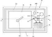
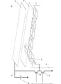
- FIG. 2 is a front view of the display device 10 shown in FIG. 3 is an exploded cross-sectional view taken along line SS shown in FIG.
- FIG. 4 is a block diagram provided in the display device 10 shown in FIG.
- FIG. 5 is a circuit diagram showing an example of a circuit mounted on the display device 10 shown in FIG.
- FIG. 6 is a front view showing a display example of the display unit 70 shown in FIG.
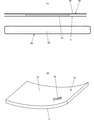
- FIG. 7A is a side view of the display device 10 shown in FIG. 1 held over the reader / writer device 50.
- FIG. 7B is a side view of the state where the display device 10 shown in FIG. 1 is bent.
- FIG. 8 is a flowchart showing operations performed by the control unit 16 shown in FIG.
- FIG. 9 is a circuit diagram showing a circuit constituting a display device 910 according to a modification of the display device 10 shown in FIG.
- FIG. 10 is a side view of a display system 200 according to the second embodiment of the present invention.
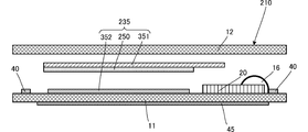
- FIG. 11 is a front view of the display device 210 shown in FIG. 12 is an exploded cross-sectional view taken along line SS shown in FIG.
- FIG. 1 is a side view of a display system 100 according to the first embodiment of the present invention.
- FIG. 2 is a front view of the display device 10 shown in FIG. 3 is an exploded cross-sectional view taken along line SS shown in FIG.
- FIG. 4 is a block diagram provided in the display device 10 shown in FIG.
- the display system 100 includes a display device 10 and a reader / writer device 50.
- the reader / writer device 50 includes a main body 52.
- the reader / writer device 50 is a so-called parent device.
- the main body 52 includes an antenna coil (not shown) that transmits and receives a radio signal, and an RFIC element (not shown) that is connected to the antenna coil and processes the radio signal.
- the display device 10 includes a base material 11, a base material 12, a control unit 16, a liquid crystal display IC 22, a display unit 70, a piezoelectric element 35, and an antenna coil 40.
- the display device 10 is a so-called child device. As shown in FIGS. 1 and 2, the display device 10 has a size and weight that are portable. Therefore, the user can carry the display device 10 by holding the display device 10 by hand.
- the piezoelectric element 35 generates an electric charge when a load is applied.
- the piezoelectric element 35 corresponds to an example of the element of the present invention.
- the reader / writer device 50 corresponds to an example of a communication device of the present invention.
- the reader / writer device 50 and the display device 10 are equipped with NFC, for example.
- NFC uses a radio signal of, for example, a 13 MHz band (HF band).
- the reader / writer device 50 and the display device 10 transmit or receive predetermined information via a magnetic field between the antenna coil 40 of the display device 10 and the antenna coil of the reader / writer device 50.
- the base material 11 is, for example, an insulating flexible plate, and is relatively strong such as polyvinyl chloride (PVC), polyethylene terephthalate (PET), polyethylene naphthalate (PEN), polycarbonate (PC), acrylic resin (PMMA), and the like. Is formed of a high polymer.
- the shape of the base material 11 is a plate shape.
- the base material 11 has flexibility, for example.
- the thickness of the base material 11 is appropriately set according to the strength required for the base material 11. Since the base material 12 has the same configuration as the base material 11, the description thereof is omitted.
- the base material 12 is bonded to the base material 11 via the piezoelectric element 35.
- circuits such as the antenna coil 40, the wiring 41A, the wiring 42A, and the planar conductor 42B are patterned on the surface of the base material 11.
- a circuit such as a shield electrode 45 is patterned on the back surface of the substrate 11. The shield electrode 45 does not overlap the antenna coil 40 when viewed from the front. The shield electrode 45 is connected to a reference potential and shields noise.
- These circuits are obtained by patterning a metal foil such as a copper foil or an aluminum foil.
- the display device 10 does not necessarily include the shield electrode 45.
- control unit 16 the liquid crystal display IC 22, the display unit 70, and the piezoelectric element 35 are mounted on the surface of the base material 11.
- the control unit 16 is connected to the antenna coil 40.
- the control unit 16 generates a first power supply voltage (for example, + several V) using the electric power obtained by the antenna coil 40.
- the control unit 16 supplies the generated first power supply voltage to the liquid crystal display IC 22 and the like. However, the control unit 16 does not supply the first power supply voltage to the display unit 70.
- the first power supply corresponds to an example of another power supply according to the present invention.
- control unit 16 processes a radio signal received by the antenna coil 40.
- the control unit 16 includes an MCU (not shown) and a flash memory (not shown).
- the control unit 16 stores amount information and ID information in the flash memory. For example, the control unit 16 instructs the liquid crystal display IC 22 so that the plurality of pixels indicate the amount information stored in the flash memory.
- the amount information is, for example, an amount (for example, 21,000 yen) charged by the user to the display device 10 as shown in FIG.
- the ID information is identification information indicating that the display device 10 corresponds to the reader / writer device 50, for example.
- the liquid crystal display IC 22 includes an interface unit 23 that communicates with the control unit 16, a switch array 25 that is connected to each pixel of the display unit 70 and switches display on and off, and a writing circuit 24 that switches the state of the switch array 25. And comprising.
- the liquid crystal display IC 22 is mounted on the mounting substrate 20 in a bare chip state and protected by a resin mold or the like.
- the mounting substrate 20 has an input terminal 21.
- the wiring for connecting the liquid crystal display IC 22 or the display unit 70 is formed on the mounting substrate 20, but these may be formed on the base material 11. The reason is that there is a difference between the dimensional accuracy of the electrode pattern formed on the substrate 11 and the dimensional accuracy of the electrode pattern formed on the mounting substrate 20.
- the electrode pattern since the electrode pattern is formed on the mounting substrate 20, the load on the electrode pattern due to the deformation of the display device 10 can be reduced.
- the nonvolatile switch array 25 is composed of a plurality of floating gate MOSFETs.
- the control unit 16 driven by the first power supply voltage communicates with the IC 22 similarly driven by the first power supply voltage, and the memory writing circuit 24 rewrites the state of the switch array 25 in accordance with an instruction from the control unit 16. Even after the first power supply voltage is lost, the state of the switch array 25 is maintained.
- the display unit 70 is composed of an LCD (liquid crystal display).
- the display unit 70 has a plurality of pixels connected to the switch array 25 and the piezoelectric element 35.
- the plurality of pixels include a pixel 172 shown in FIG.
- the piezoelectric element 35 includes a rectangular piezoelectric film 350, a GND electrode 351, and a signal electrode 352. On both main surfaces of the piezoelectric film 350, a GND electrode 351 and a signal electrode 352 are formed on substantially the entire surface.
- the GND electrode 351 is connected to the planar conductor 42B.
- the connection wiring 42A is connected to the planar conductor 42B.
- the signal electrode 352 is connected to the connection wiring 41A.
- the piezoelectric element 35 is preferably connected only to the nonvolatile switch array 25 and the display unit 70.
- the present invention includes the case where the piezoelectric element 35 is not substantially electrically connected, for example, connected to another circuit via a member having a large resistance.
- the piezoelectric element 35 is preferably connected to another circuit through the nonvolatile switch array 25.
- the antenna coil 40 and the signal electrode 352 are formed on the surface of the substrate 11. Therefore, the antenna coil 40 and the signal electrode 352 can be patterned in the same process. Thereby, the manufacturing cost of the display apparatus 10 can be reduced.
- the piezoelectric film 350 is preferably a film having piezoelectricity. More preferably, the piezoelectric film 350 is formed of uniaxially stretched polylactic acid (PLA), and further L-type polylactic acid (PLLA). In addition, the piezoelectric film 350 is preferably formed of PVDF that generates pyroelectricity.
- PLA uniaxially stretched polylactic acid
- PLLA L-type polylactic acid
- PVDF PVDF that generates pyroelectricity
- the piezoelectric film 350 is made of uniaxially stretched L-type polylactic acid (PLLA).
- PLLA uniaxially stretched L-type polylactic acid
- the piezoelectric film 350 is uniaxially stretched in a direction substantially along the diagonal line of the rectangle (see the solid arrow in FIG. 2).
- this direction is referred to as a uniaxial stretching direction 901.
- the uniaxial stretching direction 901 preferably forms an angle of 45 ° with respect to the longitudinal direction or the lateral direction of the piezoelectric film 350.
- the angle is not limited to this, and an optimum angle may be designed in consideration of the characteristics and use state of the piezoelectric film 350.
- the angle is not limited to 45 ° and may be approximately 45 °.
- About 45 ° means an angle including about 45 ° ⁇ 10 °, for example. These angles are design matters that should be determined as appropriate based on the application of the deformation sensor.
- the aforementioned PLLA is a chiral polymer, and the main chain has a helical structure.
- PLLA is uniaxially stretched and has piezoelectricity when the molecules are oriented.
- the uniaxially stretched PLLA generates electric charges when the flat film surface of the piezoelectric film is pressed. At this time, the amount of charge generated is uniquely determined by the amount of displacement of the flat membrane surface in the direction orthogonal to the flat membrane surface by pressing.
- the piezoelectric constant of uniaxially stretched PLLA belongs to a very high class among polymers.
- the piezoelectric film 350 can generate a large charge by using PLLA.
- the draw ratio is preferably about 3 to 8 times.
- PLLA generates piezoelectricity by molecular orientation processing such as stretching, and there is no need to perform poling processing like other polymers such as PVDF and piezoelectric ceramics. That is, the piezoelectricity of PLLA that does not belong to ferroelectrics is not expressed by the polarization of ions like ferroelectrics such as PVDF and PZT, but is derived from a helical structure that is a characteristic structure of molecules. is there.
- the pyroelectricity generated in other ferroelectric piezoelectric materials does not occur in PLLA.
- PVDF or the like shows a change in piezoelectric constant over time, and in some cases, the piezoelectric constant may be significantly reduced, but the piezoelectric constant of PLLA is extremely stable over time. Therefore, the piezoelectric film 350 can generate a very high charge without being affected by the surrounding environment.
- the signal electrode 352 and the shield electrode 45 are made of, for example, copper foil or aluminum foil.
- the GND electrode 351 is made of, for example, a conductive nonwoven film.
- the GND electrode 351 is formed on one main surface of the piezoelectric film 350 by silver printing.
- the GND electrode 351 and the signal electrode 352 have a large deformation of the base material 11, so that an organic electrode mainly composed of ITO, ZnO, polythiophene, an organic electrode mainly composed of polyaniline, a silver nanowire electrode, a carbon nanotube electrode, etc. Can also be used. By using these materials, an electrode pattern excellent in flexibility can be formed.
- FIG. 5 is a circuit diagram showing an example of a circuit mounted on the display device 10 shown in FIG.
- FIG. 6 is a front view showing a display example of the display unit 70 shown in FIG. As shown in FIG. 5, this circuit includes a piezoelectric element 35, a floating gate MOSFET 81, a floating gate MOSFET 82, a plurality of lower electrodes 71, a liquid crystal layer 72, and an upper electrode 73.
- FIG. 5 shows the circuit mounted on the display device 10 as an example, it is not limited to this. In implementation, the display device may include other circuits.
- the display unit 70 includes an upper electrode 73, a liquid crystal layer 72, and a plurality of lower electrodes 71.
- the upper electrode 73 is a flat transparent electrode.
- the plurality of lower electrodes 71 are electrodes showing a 7-segment numerical value.
- the display unit 70 includes a plurality of pixels including one pixel 172.
- the display unit 70 represents a 7-segment numerical value by a plurality of pixels.
- the display unit 70 has a static drive method that draws lines from all pixels.
- the display unit 70 is preferably formed of, for example, a reflective liquid crystal that does not require a backlight, instead of a transmissive liquid crystal that requires a backlight. Moreover, it is preferable that the display part 70 is comprised with the polymer dispersion type liquid crystal which does not require a polarizing plate, for example.
- the piezoelectric element 35 is connected to the upper electrode 73 as shown in FIG.
- the plurality of lower electrodes 71 are connected to the nonvolatile switch array 25.
- the lower electrode 171 that is one of the plurality of lower electrodes 71 is connected to a wiring that connects the floating gate MOSFET 81 and the floating gate MOSFET 82.
- the lower electrode 171 is an electrode constituting the pixel 172.
- the floating gate MOSFET 81 and the floating gate MOSFET 82 are connected in series with the piezoelectric element 35.
- the liquid crystal display IC 22 rewrites the states of the floating gate MOSFET 81 and the floating gate MOSFET 82 in accordance with instructions from the control unit 16. Communication with the control unit 16 and energy necessary for driving the writing circuit 24 are all provided by the first power supply voltage.
- the liquid crystal display IC 22 turns off the floating gate MOSFET 81 when turning on the floating gate MOSFET 82 and turns off the floating gate MOSFET 82 when turning on the floating gate MOSFET 81 so that the floating gate MOSFET 81 and the floating gate MOSFET 82 are complementary. To do. Therefore, when the floating gate MOSFET 82 is off and the floating gate MOSFET 81 is on, the second power supply voltage is applied to the liquid crystal sandwiched between the upper electrode 73 and the lower electrode 171.
- the floating gate MOSFET 81 when the floating gate MOSFET 81 is off and the floating gate MOSFET 82 is on, the upper electrode 73 and the lower electrode 171 have the same potential, so that the second power supply voltage is applied to the liquid crystal sandwiched between the upper electrode 73 and the lower electrode 171. Not applied.
- the lower electrode 171 By adopting such a complementary configuration, it is possible to prevent the lower electrode 171 from having a floating potential in any state and causing an unintended operation.
- the lower electrode 171 becomes a floating potential when the floating gate MOSFET 81 is turned off.
- the electrode 171 approaches the GND potential, and a voltage is applied to the liquid crystal despite the floating gate MOSFET 81 being off.
- the plurality of floating gate MOSFETs function as passive components as a collection of switches.
- the state of each pixel is determined by the state of each switch. Therefore, pixel display is possible without requiring the first power supply voltage.
- a normal liquid crystal display device has a dynamic drive system in which electrodes of each pixel are connected in a matrix so that a large number of pixels can be controlled with a small number of lead lines, and a voltage is applied while scanning each pixel. It is driven by.
- a separate driving IC and a clock signal for driving the IC are required.
- the electric power generated by the piezoelectric element 35 is small, and it is difficult to generate a clock signal with this electric power.
- the display device 10 draws an electrode from each pixel of the liquid crystal and includes a nonvolatile switch so that predetermined information is statically displayed. Accordingly, the display unit 70 can display with a plurality of pixels even with a small electric power generated by the piezoelectric element 35.
- the polymer-dispersed liquid crystal has a slow change in optical characteristics with respect to voltage as compared with a commonly used TN liquid crystal. Therefore, when the dynamic drive method is applied to the polymer dispersion type liquid crystal, the contrast may be lowered. Therefore, it is advantageous to apply the static display method as described above.
- the piezoelectric element 35 is charged by the piezoelectric film 350 being bent. appear. This charge is detected by the GND electrode 351 and the signal electrode 352.
- the charges detected by the GND electrode 351 and the signal electrode 352 are input to the liquid crystal display IC 22 via the connection wiring 41A, the planar conductor 42B, and the connection wiring 42A.
- a voltage (second power supply voltage) based on the charge input to the liquid crystal display IC 22 is applied to the display unit 70 via the liquid crystal display IC 22.
- the electric charge generated when the user bends the piezoelectric element 35 once is 20 nC, for example, and the second power supply voltage is 10 V, for example.
- the display unit 70 applies a voltage based on the electric charge generated in the piezoelectric element 35 to a plurality of pixels, and displays information by the plurality of pixels. Thereby, the display unit 70 displays “21000”, which is the amount information, by a plurality of pixels as shown in FIG. 6, for example.
- the display device 10 and the display system 100 can perform pixel display only by the voltage generated in the display device 10, it is not necessary to mount a battery for display.
- the user can confirm the currently charged amount (for example, 21,000 yen) by bending the display device 10 as shown in FIG.
- the liquid crystal display IC 22 and the display unit 70 may be mounted on any main surface of the base material 11 and the base material 12, but are preferably disposed on the same surface as the surface on which the piezoelectric element 35 is disposed. By disposing them on the same surface, the piezoelectric element 35, the liquid crystal display IC 22 and the display unit 70 can be connected without using an interlayer connection conductor such as a via. Thereby, the display apparatus 10 can be comprised at low cost.
- the user brings the display device 10 closer to the reader / writer device 50 installed in the store.
- the user charges the display device 10 in advance with a predetermined amount (for example, 22,000 yen).
- FIG. 8 is a flowchart showing an operation performed by the control unit 16 shown in FIG.
- the reader / writer device 50 transmits a polling command for requesting a response to the display device 10 located in the communication area every predetermined time (for example, every 10 ms).
- control unit 16 When the control unit 16 receives the polling command, the control unit 16 transmits a response to the reader / writer device 50 (S1). Thereby, communication between the control unit 16 and the reader / writer device 50 starts.
- the control unit 16 determines whether an ID request command has been transmitted from the reader / writer device 50 (S2).
- the ID request command is a command for requesting transmission of ID information.
- the control unit 16 ends this processing when the ID request command is not transmitted from the reader / writer device 50 within a predetermined time (for example, 5 seconds).
- the control unit 16 ends the communication with the reader / writer device 50.
- the control unit 16 transmits the ID information (S3).
- the reader / writer device 50 identifies the display device 10 based on the ID information.
- the ID information is identification information indicating that the display device 10 corresponds to the reader / writer device 50, for example.
- the control unit 16 determines whether or not the commodity price information has been transmitted from the reader / writer device 50 (S4).
- the amount information of the product is, for example, 1000 yen.
- S4 assumes a scene in which the store clerk inputs the price information of the product purchased by the user into the reader / writer device 50.
- control unit 16 ends this process.
- the control unit 16 ends the communication with the reader / writer device 50.
- the control unit 16 determines the commodity price (for example, 1000 yen) from the currently charged price (for example, 22,000 yen). Yen) is subtracted (S5). The subtracted amount data is written to a flash memory built in the control unit 16 and sent to the liquid crystal display IC 22. The sent data is converted into pixel information in the liquid crystal display IC 22, and the state of the switch array 25 in the liquid crystal display IC is switched.
- the user can confirm the currently charged amount (for example, 21,000 yen) by bending the display device 10 as shown in FIG. 7B, for example. At this time, the reader / writer device 50 is not necessary.
- FIG. 9 is a circuit diagram showing a circuit constituting a display device 910 according to a modification of the display device 10 shown in FIG.
- the difference between the display device 910 and the display device 10 is a circuit. Since other configurations are the same, description thereof is omitted.
- the circuit includes a piezoelectric element 35, a floating gate MOSFET 81, a plurality of lower electrodes 71, a liquid crystal layer 72, and an upper electrode 73, as shown in FIG. Unlike the circuit shown in FIG. 5, this circuit does not have the aforementioned floating gate MOSFET 82.
- the piezoelectric element 35 is connected to the upper electrode 73 as shown in FIG.
- the plurality of lower electrodes 71 are not connected to the piezoelectric element 35 via the plurality of floating gate MOSFETs.
- the lower electrode 171 that is one of the plurality of lower electrodes 71 is connected to the source terminal of the floating gate MOSFET 81.
- the lower electrode 171 is not connected to the floating gate MOSFET 82.
- the leakage current in the order of pA is smaller than the electric power (charge amount) generated by the piezoelectric element, and is not so problematic for displaying for several seconds.
- the life of a liquid crystal is said to be shortened when a DC signal is applied, and it is used by applying an AC signal.
- a reverse charge voltage
- the liquid crystal display disappears. Since no DC signal is applied for a long time, this problem does not occur. Even if the bending is continued, the generated charge is eventually lost due to the leakage current, and thus a DC voltage is not applied to the display unit 70 for a long time.
- the signal generated by the piezoelectric element 35 may be applied to the display unit 70 or the liquid crystal display IC 22 after being rectified by a diode or the like.
- a unidirectional voltage can be applied to the IC regardless of which direction it is bent, or it can respond only to a unidirectional bend. Further, by optimizing the circuit, another display can be made when bent in the opposite direction.
- FIG. 10 is a side view of the display system 200 according to the second embodiment of the present invention.
- FIG. 11 is a front view of the display device 210 shown in FIG. 12 is an exploded cross-sectional view taken along line SS shown in FIG.
- the display system 200 according to the second embodiment is different from the display system 100 according to the first embodiment in that a piezoelectric element 235 that generates an electric charge when twisted instead of the piezoelectric element 35 that generates an electric charge when bent. It is the display apparatus 210 provided with.
- the piezoelectric element 235 is different from the piezoelectric element 35 in the piezoelectric film 250. Since the other points of the display system 200 are the same as those of the first embodiment, description thereof is omitted.
- the uniaxial stretching direction 902 of the piezoelectric film 250 is different from the uniaxial stretching direction 901 of the piezoelectric film 350.
- the uniaxial stretching direction 902 of the piezoelectric film 250 preferably forms an angle of 45 ° with respect to the diagonal line of the substrate 11.
- the uniaxial stretching direction 902 may form an angle of 0 ° with respect to the longitudinal direction or the lateral direction of the substrate 11.
- the angle is not limited to this, and an optimum angle may be designed in consideration of the characteristics and use state of the piezoelectric film 250.
- 0 ° In addition, it is not limited to the exact 0 °, but may be almost 0 °. Substantially 0 ° means an angle including about 0 ° ⁇ 10 °, for example. These angles are design matters to be appropriately determined based on the use of the piezoelectric element.
- the display device 210 When a pressure causing twist is applied to the display device 210, the display device 210 is twisted about the uniaxial stretching direction 902 as an axis. In this case, the piezoelectric film 250 of the piezoelectric element 235 expands or contracts. Thereby, a change occurs in the voltage output from the piezoelectric element 235 due to torsional deformation.
- the piezoelectric element 235 when the user deforms the piezoelectric film 250 by twisting the base material 11 and the base material 12, the piezoelectric element 235 generates electric charges due to the deformation of the piezoelectric film 250.
- This charge is detected by the GND electrode 351 and the signal electrode 352.
- the charges detected by the GND electrode 351 and the signal electrode 352 are input to the liquid crystal display IC 22 via the connection wiring 41A, the planar conductor 42B, and the connection wiring 42A.
- a voltage (second power supply voltage) based on the electric charge input to the liquid crystal display IC 22 is applied to the display unit 70 via the liquid crystal display IC 22.
- the display unit 70 applies a voltage based on the electric charge generated in the piezoelectric element 235 to a plurality of pixels, and displays information by the plurality of pixels. Thereby, the display unit 70 displays “21000”, which is the amount information, by a plurality of pixels as shown in FIG. 6, for example.
- the display device 210 and the display system 200 can perform pixel display only by the voltage generated in the display device 210, it is not necessary to mount a battery for display. For example, the user can check the currently charged amount (for example, 21,000 yen) by twisting the display device 210.
- the display device 10 includes the piezoelectric element 35 and the display device 210 includes the piezoelectric element 235.
- the display device may include a pyroelectric element that generates an electric charge when a temperature change is applied, instead of the above-described piezoelectric element.
- the piezoelectric element 35 and the piezoelectric element 235 are composed of the piezoelectric film 350.
- the present invention is not limited to this.
- the piezoelectric element may be composed of a piezoelectric ceramic or the like.
- the base material 11 and the base material 12 are molded with a hard material such as plastic, but the present invention is not limited to this.
- the base material 11 and the base material 12 may be formed of a soft material such as a film, for example.
- the display unit 70 displays the money amount information with a plurality of pixels, but the present invention is not limited to this.
- the display unit 70 may display other information (for example, character information or barcode) with a plurality of pixels.
Landscapes
- Engineering & Computer Science (AREA)
- Physics & Mathematics (AREA)
- General Physics & Mathematics (AREA)
- Theoretical Computer Science (AREA)
- Computer Hardware Design (AREA)
- Microelectronics & Electronic Packaging (AREA)
- Spectroscopy & Molecular Physics (AREA)
- Devices For Indicating Variable Information By Combining Individual Elements (AREA)
- Control Of Indicators Other Than Cathode Ray Tubes (AREA)
Abstract
表示装置内で発生させた電圧を利用することによって消費電力を削減できる表示装置及び表示システムを提供する。 表示装置(10)は、基材(11)と基材(12)と制御部(16)と液晶表示(IC22)と表示部(70)と圧電素子(35)とアンテナコイル(40)とを備える。表示部(70)は、複数のフローティングゲート(MOSFET)を介して圧電素子(35)に接続する複数の画素を有する。利用者が圧電フィルム(350)を変形させたとき、圧電素子(35)は、圧電フィルム(350)が撓んで電荷を発生する。表示部(70)は、圧電素子(35)で発生した電荷に基づく電圧を複数の画素に印加し、情報を複数の画素によって表示する。これにより、表示部(70)は例えば、金額情報である「21000」を複数の画素によって表示する。
Description
本発明の一実施形態は、情報を複数の画素によって表示する表示装置、及び当該表示装置を備える表示システムに関する。
従来、情報を複数の画素によって表示する表示装置が普及している。例えば特許文献1は、液晶パネルを有する表示部と、残金等を記憶する記憶部と、警告音等を発生する音発生部と、各部を制御する制御部と、各部に電源を供給する電源部とを備えるICカードを開示している。表示部は、電源部から供給される電源に基づいて、残金、合計金額等を液晶パネルによって表示する。
しかしながら、特許文献1のICカードは、持ち運び可能であるため、電源部として電池等を備える必要がある。そのため、特許文献1のICカードは、できるだけ消費電力を削減する必要がある。
本発明の一実施形態の目的は、表示装置内で発生させた電圧を利用することによって消費電力を削減できる表示装置及び表示システムを提供することにある。
本発明の一実施形態に係る表示装置は、負荷が加えられたときに電荷を発生する素子と、素子に接続する複数の画素を有する表示部と、を備える。表示部は、素子で発生した電荷に基づく電圧を複数の画素に印加し、情報を複数の画素によって表示する。
この構成では素子に負荷が加えられたとき、素子では電荷が発生する。素子で発生した電荷は、表示部に入力する。表示部に入力した電荷に基づく電圧(第2電源電圧)は、複数の画素に印加される。これにより表示部は、情報を複数の画素によって表示する。
したがって、表示装置は、表示装置内で発生させた電圧を利用することによって消費電力を削減できる。
また、本発明の一実施形態に係る表示システムは、本発明の一実施形態に係る表示装置と、通信装置と、を備える。通信装置は、表示装置と無線通信を行う。
本発明の一実施形態に係る表示システムは、本発明の一実施形態に係る表示装置を備えるため、本発明の一実施形態に係る表示装置と同様の効果を奏する。
本発明の一実施形態は、表示装置内で発生させた電圧を利用することによって消費電力を削減できる。
本発明の第1実施形態に係る表示装置及び表示システムについて説明する。図1は、本発明の第1実施形態に係る表示システム100の側面図である。図2は、図1に示す表示装置10の正面図である。図3は、図2に示すS-S線の分解断面図である。図4は、図1に示す表示装置10が備えるブロック図である。表示システム100は、図1に示すように、表示装置10とリーダライタ装置50とを備える。
リーダライタ装置50は、本体52を備える。リーダライタ装置50は、所謂親機である。本体52は、無線信号を送受するアンテナコイル(不図示)と、当該アンテナコイルに接続し、無線信号を処理するRFIC素子(不図示)と、を内蔵する。
表示装置10は、基材11と、基材12と、制御部16と、液晶表示IC22と、表示部70と、圧電素子35と、アンテナコイル40と、を備える。表示装置10は、所謂子機である。表示装置10は、図1、図2に示すように、携帯可能な程度の大きさ及び重さからなる。そのため、利用者は、表示装置10を手で持って表示装置10を持ち運ぶことができる。圧電素子35は、負荷が加えられたときに電荷を発生する。
なお、圧電素子35は、本発明の素子の一例に相当する。リーダライタ装置50は、本発明の通信装置の一例に相当する。
リーダライタ装置50及び表示装置10は例えばNFCを搭載している。NFCは例えば13MHz帯(HF帯)の無線信号を利用している。リーダライタ装置50及び表示装置10は、表示装置10のアンテナコイル40とリーダライタ装置50のアンテナコイルとの間で磁界を介して、所定の情報を送信又は受信する。
基材11は、例えば絶縁性の可撓板であり、ポリ塩化ビニル(PVC)、ポリエチレンテレフタレート(PET)、ポリエチレンナフタレート(PEN)、ポリカーボネート(PC)、アクリル樹脂(PMMA)等の比較的強度が高いポリマーで形成されている。基材11の形状は板状である。基材11は例えば可撓性を有する。基材11の厚みは、基材11に必要とされる強度に応じて適宜設定されている。基材12は、基材11と同じ構成であるため、説明を省略する。基材12は、圧電素子35を介して基材11と接合している。
基材11の表面には、図2に示すように、アンテナコイル40、配線41A、配線42A、及び平面導体42B等の回路がパターンニングされている。基材11の裏面には、図3に示すように、シールド電極45等の回路がパターンニングされている。シールド電極45は正面視してアンテナコイル40と重ならない。シールド電極45は、基準電位に接続され、ノイズを遮蔽する。これらの回路は、銅箔、アルミ箔などの金属箔をパターンニングしたものである。
なお、表示装置10は、必ずしもシールド電極45を備える必要がない。
さらに、基材11の表面には、制御部16、液晶表示IC22、表示部70、及び圧電素子35が実装されている。制御部16は、アンテナコイル40に接続する。制御部16は、アンテナコイル40によって得た電力により第1電源電圧(例えば+数V)を生成する。制御部16は、生成した第1電源電圧を液晶表示IC22等に供給する。しかし、制御部16は、第1電源電圧を表示部70に供給しない。
なお、第1電源は、本発明の別の電源の一例に相当する。
また、制御部16は、アンテナコイル40で受信した無線信号を処理する。制御部16は、MCU(不図示)とフラッシュメモリ(不図示)とを有する。制御部16は、金額情報及びID情報をフラッシュメモリに保存している。制御部16は例えば、複数の画素が、フラッシュメモリに保存している金額情報を示すよう液晶表示IC22に指示する。
なお、金額情報は例えば後述の図6に示すように、利用者が表示装置10にチャージしている金額(例えば21000円)などである。ID情報は例えば、表示装置10がリーダライタ装置50に対応することを示す識別情報である。
液晶表示IC22は、制御部16と通信するためのインターフェイス部23と、表示部70の各画素に接続されて表示のオンオフを切り替えるスイッチアレイ25と、スイッチアレイ25の状態を切り替えるための書き込み回路24と、を備える。液晶表示IC22は、ベアチップの状態で実装基板20に実装され、樹脂モールドなどで保護される。実装基板20は入力端子21を有する。第1実施形態では、実装基板20の上に液晶表示IC22又は表示部70を接続する配線が形成されているが、これらについては基材11上に形成されても良い。その理由は、基材11上に形成する電極パターンの寸法精度と実装基板20上に形成される電極パターンの寸法精度とに違いがあるためである。また、電極パターンが実装基板20上に形成されることによって、表示装置10の変形による電極パターンへの負荷を減らすことができる。
不揮発性スイッチアレイ25は、複数のフローティングゲートMOSFETから構成される。第1電源電圧によって駆動された制御部16と、同じく第1電源電圧によって駆動されたIC22が通信し、制御部16の指示にしたがって、メモリ書き込み回路24がスイッチアレイ25の状態を書き換える。第1電源電圧が失われた後も、スイッチアレイ25の状態は保持される。
表示部70は、LCD(liquid crystal display)で構成される。表示部70は、スイッチアレイ25と圧電素子35に接続する複数の画素を有する。複数の画素は後述の図6に示す画素172を含む。
圧電素子35は、図3に示すように、矩形状の圧電フィルム350とGND電極351と信号電極352とを備える。圧電フィルム350の両主面にはそれぞれGND電極351、信号電極352が略全面に形成されている。GND電極351は平面導体42Bに接続している。そして、接続配線42Aは平面導体42Bに接続している。また、信号電極352は接続配線41Aに接続している。圧電素子35は、不揮発性スイッチアレイ25及び表示部70のみと接続することが好ましい。圧電素子35が発生する電圧は小さいため、メモリ書き込み回路24などの別回路に直接つながる配線がある場合、不揮発性スイッチアレイ25に十分な電力を供給できなくなるおそれがある。そこで、上述のような接続にすることによって、より確実に表示部70へ情報を表示させることができる。なお、圧電素子35が、例えば抵抗の大きな部材を介して別回路に接続するなど、実質上電気的に接続されていない場合であっても本発明に含まれる。また、圧電素子35は不揮発性スイッチアレイ25を介して別回路に接続されていることが好ましい。
なお、アンテナコイル40及び信号電極352は、基材11の表面に形成されている。そのため、アンテナコイル40及び信号電極352は、同一工程でパターニングすることが可能である。これにより、表示装置10の製造コストを削減できる。
また、圧電フィルム350は、圧電性を有するフィルムであることが好ましい。圧電フィルム350は、一軸延伸されたポリ乳酸(PLA)、さらにはL型ポリ乳酸(PLLA)によって形成されていることがさらに好ましい。その他、圧電フィルム350は、焦電性を生じるPVDFによって形成されていることが好ましい。
圧電フィルム350は、一軸延伸されたL型ポリ乳酸(PLLA)によって形成されている。本実施形態では、圧電フィルム350は、矩形の対角線にほぼ沿った方向に一軸延伸されている(図2の実線の中抜き矢印参照)。この方向を、以下では、一軸延伸方向901と称する。一軸延伸方向901は、圧電フィルム350の長手方向又は短手方向に対して45°の角度を成すことが好ましい。ただし、角度はこれに限るものではなく、圧電フィルム350の特性や使用状態に鑑みて最適な角度に設計すればよい。
なお、正確な45°に限ることなく、略45°でもよい。略45°とは、例えば45°±10°程度を含む角度をいう。これらの角度は、変形センサの用途に基づき、適宜決定されるべき設計事項である。
前述のPLLAは、キラル高分子であり、主鎖が螺旋構造を有する。PLLAは、一軸延伸され、分子が配向すると、圧電性を有する。そして、一軸延伸されたPLLAは、圧電フィルムの平膜面が押圧されることにより、電荷を発生する。この際、発生する電荷量は、押圧により平膜面が、当該平膜面に直交する方向へ変位する変位量によって一意的に決定される。一軸延伸されたPLLAの圧電定数は、高分子中で非常に高い部類に属する。
したがって、圧電フィルム350は、PLLAを用いることで、大きい電荷を発生することができる。
なお、延伸倍率は3~8倍程度が好適である。延伸後に熱処理を施すことにより、ポリ乳酸の延びきり鎖結晶の結晶化が促進され圧電定数が向上する。なお、二軸延伸した場合はそれぞれの軸の延伸倍率を異ならせることによって一軸延伸と同様の効果を得ることができる。例えばある方向をX軸としてその方向に8倍、その軸に直交するY軸方向に2倍の延伸を施した場合、圧電定数に関してはおよそX軸方向に4倍の一軸延伸を施した場合と同等の効果が得られる。単純に一軸延伸したフィルムは延伸軸方向に沿って裂け易いため、前述したような二軸延伸を行うことにより幾分強度を増すことができる。
また、PLLAは、延伸等による分子の配向処理で圧電性を生じ、PVDF等の他のポリマーや圧電セラミックスのように、ポーリング処理を行う必要がない。すなわち、強誘電体に属さないPLLAの圧電性は、PVDFやPZT等の強誘電体のようにイオンの分極によって発現するものではなく、分子の特徴的な構造である螺旋構造に由来するものである。
このため、PLLAには、他の強誘電性の圧電体で発生する焦電性が生じない。さらに、PVDF等は経時的に圧電定数の変動が見られ、場合によっては圧電定数が著しく低下する場合があるが、PLLAの圧電定数は経時的に極めて安定している。したがって、圧電フィルム350は、周囲環境に影響されることなく、非常に高い電荷を発生することが可能になる。
また、PLLAは圧電出力定数(=圧電g定数、g=d/εT)が大きい。したがって、圧電フィルム350は、PLLAを用いることで、非常に高い電圧を発生することが可能になる。
また、信号電極352及びシールド電極45は例えば、銅箔、アルミ箔から構成される。GND電極351は例えば、導電性不織布フィルムから構成される。GND電極351は例えば、圧電フィルム350の一方主面に銀印刷で形成される。
なお、GND電極351、信号電極352は、基材11が大きく変形するため、ITO、ZnO、ポリチオフェンを主成分とする有機電極、ポリアニリンを主成分とする有機電極、銀ナノワイヤ電極、カーボンナノチューブ電極などを用いることもできる。これらの材料を用いることで、屈曲性に優れた電極パターンを形成できる。
以下、表示装置10に実装される回路について説明する。
図5は、図2に示す表示装置10に実装される回路の一例を示す回路図である。図6は、図2に示す表示部70の表示例を示す正面図である。この回路は、図5に示すように、圧電素子35とフローティングゲートMOSFET81とフローティングゲートMOSFET82と複数の下部電極71と液晶層72と上部電極73とを含んでいる。
なお、図5は表示装置10に実装される回路を一例として示しているが、これに限るものではない。実施の際、表示装置は、他の回路を備えてもよい。
表示部70は図5に示すように、上部電極73と液晶層72と複数の下部電極71とを備える。上部電極73は平板状の透明電極である。複数の下部電極71は、7セグメント式の数値を示す電極である。
上部電極73及び複数の下部電極71は、液晶層72を挟んでいる。表示部70は図6に示すように、1つの画素172を含む複数の画素を有する。表示部70は、7セグメント式の数値を複数の画素によって表している。表示部70は、全ての画素から線を引き出すスタティック駆動方式を有する。
なお、表示部70は例えば、バックライトを必要とする透過型液晶でなく、バックライトを必要としない反射型液晶によって構成されていることが好ましい。また、表示部70は例えば、偏光板を必要としない高分子分散型液晶によって構成されていることが好ましい。
圧電素子35は図5に示すように、上部電極73に接続している。複数の下部電極71は、不揮発スイッチアレイ25に接続している。例えば複数の下部電極71のうちの1つである下部電極171は、フローティングゲートMOSFET81及びフローティングゲートMOSFET82を接続する配線に接続している。下部電極171は、画素172を構成する電極である。フローティングゲートMOSFET81及びフローティングゲートMOSFET82は、圧電素子35と直列に接続している。
液晶表示IC22は、制御部16の指示にしたがって、フローティングゲートMOSFET81及びフローティングゲートMOSFET82の状態を書き換える。制御部16との通信、及び、書き込み回路24を駆動させるために必要なエネルギーは、すべて第1の電源電圧によって賄われる。
そして、液晶表示IC22は例えば、フローティングゲートMOSFET81及びフローティングゲートMOSFET82が相補的になるよう、フローティングゲートMOSFET82をオンするときはフローティングゲートMOSFET81をオフし、フローティングゲートMOSFET81をオンするときはフローティングゲートMOSFET82をオフする。そのため、フローティングゲートMOSFET82がオフでフローティングゲートMOSFET81がオンであるとき、上部電極73及び下部電極171に挟まれた液晶に第2の電源電圧が印加される。
一方、フローティングゲートMOSFET81がオフでフローティングゲートMOSFET82がオンであるとき、上部電極73及び下部電極171は同電位となるため、上部電極73及び下部電極171に挟まれた液晶に第2の電源電圧が印加されない。このような相補的な構成とすることで、いずれの状態においても、下部電極171が浮き電位となって、意図しない動作となることを防ぐことができる。
図9のように、フローティングゲートMOSFET82が存在せず、フローティングゲートMOSFET81のみで構成した場合、フローティングゲートMOSFET81がオフの時に下部電極171が浮き電位となるが、フローティングゲートMOSFET81のリーク電流によって、やがて下部電極171はGND電位に近づき、フローティングゲートMOSFET81がオフであるのにもかかわらず、液晶には電圧が印加されてしまうことになる。
ここで、オンとオフを切り替えられた後、複数のフローティングゲートMOSFETは、スイッチの集合体として受動部品として機能する。第2の電源電圧が印加されたとき、各スイッチの状態により各画素の状態が決定される。そのため、第1の電源電圧を必要とすることなく、画素表示が可能になる。
なお、通常の液晶表示装置は、少ない引き出し線で多くの画素をコントロールできるように各画素の電極がマトリックス状に接続されており、各画素を走査(スキャン)しながら電圧を印加するダイナミック駆動方式で駆動されている。しかし、ダイナミック駆動方式で駆動するためには、別途駆動用のICと、ICを駆動するためのクロック信号とが必要になる。
しかし、圧電素子35で発生する電力は小さく、この電力ではクロック信号を生成することが難しい。
そこで、表示装置10は、液晶の各画素から電極を引き出し、不揮発性のスイッチを備え、所定の情報を静的に表示させるようにしている。これにより、表示部70は、圧電素子35で発生した小さい電力であっても、複数の画素によって表示することができる。また、高分子分散型液晶は、一般的に用いられているTN液晶と比べて電圧に対する光学特性の変化が緩慢である。したがって、高分子分散型液晶にダイナミック駆動方式を適用するとコントラストが低下する場合があるため、上述のような静的な表示方式を適用する方が有利である。
以上の構成において、利用者が図7(B)に示すように基材11及び基材12を曲げることにより圧電フィルム350を変形させたとき、圧電素子35は、圧電フィルム350が撓んで電荷を発生する。この電荷は、GND電極351及び信号電極352で検知される。GND電極351及び信号電極352で検知された電荷は、接続配線41A、平面導体42B及び接続配線42Aを介して液晶表示IC22に入力する。
液晶表示IC22に入力した電荷に基づく電圧(第2電源電圧)は、液晶表示IC22を介して表示部70に印加される。ここで、利用者が圧電素子35を1回曲げたときに発生する電荷は例えば20nCであり、第2電源電圧は例えば10Vである。
すなわち表示部70は、圧電素子35で発生した電荷に基づく電圧を複数の画素に印加し、情報を複数の画素によって表示する。これにより、表示部70は例えば図6に示すように、金額情報である「21000」を複数の画素によって表示する。
したがって、表示装置10及び表示システム100は、表示装置10内で発生させた電圧のみによって画素表示が可能なため、表示のために電池を搭載する必要が無い。利用者は例えば、図7(B)に示すように表示装置10を曲げることによって、現在チャージされている金額(例えば21000円)を確認できる。
なお、液晶表示IC22及び表示部70は基材11及び基材12におけるどの主面に実装されていてもよいが、圧電素子35が配置されている面と同じ面に配置することが好ましい。同じ面に配置することによって、ビアなどの層間接続導体を使用することなく圧電素子35と液晶表示IC22及び表示部70とを接続することができる。これにより、表示装置10を安価に構成することができる。
次に、利用者が表示装置10を使って商品を店で購入する場面について説明する。利用者は商品を購入する時、表示装置10を、店に設置されたリーダライタ装置50に近づける。なお、利用者は、所定の金額(例えば22000円)を表示装置10に予めチャージしていることとする。
図8は、図2に示す制御部16が行う動作を示すフローチャートである。リーダライタ装置50は、所定時間毎(例えば、10ms毎)に通信領域内に位置する表示装置10に対して応答を要求するポーリングコマンドを送信している。
制御部16がポーリングコマンドを受信したとき、制御部16は応答をリーダライタ装置50に送信する(S1)。これにより、制御部16とリーダライタ装置50との通信が開始する。
なお、S1では、図7(A)に示すように、利用者が表示装置10をリーダライタ装置50の上にかざした場面を想定している。
制御部16は、ID要求コマンドがリーダライタ装置50から送信されてきたか否かを判定する(S2)。ID要求コマンドとは、ID情報の送信を要求するコマンドである。
制御部16は、所定時間(例えば5秒)以内にID要求コマンドがリーダライタ装置50から送信されてこなかったとき、本処理を終了する。制御部16は、リーダライタ装置50との通信を終了する。
一方、制御部16は、所定時間(例えば5秒)以内にID要求コマンドがリーダライタ装置50から送信されてきたとき、ID情報を送信する(S3)。リーダライタ装置50は、ID情報を受信すると、ID情報に基づいて表示装置10を識別する。ID情報は例えば、表示装置10がリーダライタ装置50に対応することを示す識別情報である。
制御部16は、商品の金額情報がリーダライタ装置50から送信されてきたか否かを判定する(S4)。商品の金額情報は例えば1000円である。
S4は、店員が、利用者が購入した商品の金額情報をリーダライタ装置50に入力した場面を想定している。
S4において所定時間(例えば5秒)以内に商品の金額情報がリーダライタ装置50から送信されてこなかったとき、制御部16は、本処理を終了する。制御部16は、リーダライタ装置50との通信を終了する。
S4において所定時間(例えば5秒)以内に商品の金額情報がリーダライタ装置50から送信されてきたとき、制御部16は、現在チャージされている金額(例えば22000円)から商品の金額(例えば1000円)を減算する(S5)。減算された金額データは、制御部16に内蔵しているフラッシュメモリに書き込まれるとともに、液晶表示IC22に送られる。送られたデータは液晶表示IC22内で画素情報に変換され、液晶表示IC内のスイッチアレイ25の状態を切り替える。
したがって、利用者は以後、例えば、図7(B)に示すように表示装置10を曲げることによって、現在チャージされている金額(例えば21000円)を確認できる。この時、リーダライタ装置50は必要ない。
次に、表示装置10の変形例に係る表示装置910について説明する。
図9は、図2に示す表示装置10の変形例に係る表示装置910を構成する回路を示す回路図である。表示装置910が表示装置10と相違する点は、回路である。その他の構成については同じであるため説明を省略する。
この回路は図9に示すように、圧電素子35とフローティングゲートMOSFET81と複数の下部電極71と液晶層72と上部電極73とを含んでいる。この回路は、図5に示す回路と異なり、前述のフローティングゲートMOSFET82を有さない。
圧電素子35は図5に示すように、上部電極73に接続している。複数の下部電極71は、複数のフローティングゲートMOSFETを介して圧電素子35に接続していない。例えば複数の下部電極71のうちの1つである下部電極171は、フローティングゲートMOSFET81のソース端子に接続している。下部電極171は、フローティングゲートMOSFET82に接続していない。
以上より図9に示す回路では、フローティングゲートMOSFET81にわずかなリーク電流がある。リーク電流は、数pAオーダーの電流であるが、1画素あたりの静電容量は極めて小さいため、画素は短時間でチャージアップしてしまう。そのため、フローティングゲートMOSFET81がオフされているときも、液晶に電圧が印加される虞がある。
一方、図5に示す回路ではフローティングゲートMOSFET81及びフローティングゲートMOSFET82のスイッチ状態が相補的であるため、オフされているフローティングゲートMOSFETに多少のリーク電流があっても、オンされているフローティングゲートMOSFETの電位が液晶に印加される。
ただし、pAオーダーのリーク電流は、圧電素子が発生させる電力(電荷量)に比べると小さく、数秒程度の表示にはそれほど問題にはならない。
一般的に液晶は、直流信号を印加すると寿命が短くなるとされており、交流信号を印加して用いられる。今回の発明では、表示装置10を曲げることにより残金などが表示されたのち、曲げを解除して元の形状に戻すと、逆方向の電荷(電圧)が発生し、液晶表示は消えることになり、長時間直流信号が印加されることが無いため、この問題が生じない。曲げ続けたとしても、発生電荷はリーク電流によってやがて失われるので、表示部70に直流電圧が長時間印加されることが無い。
圧電素子35で発生した信号は、ダイオードなどで整流した後に表示部70や液晶表示IC22に印加されてもよい。この場合、どちらの向きに曲げてもICに一方向の電圧が印加されるようにもできるし、一方向の曲げだけに反応するようにもできる。また回路を最適化することによって、逆向きに曲げたときには別の表示がされるように構成することもできる。
以下、本発明の第2実施形態に係る表示装置及び表示システムについて説明する。
図10は、本発明の第2実施形態に係る表示システム200の側面図である。図11は、図10に示す表示装置210の正面図である。図12は、図11に示すS-S線の分解断面図である。
第2実施形態の表示システム200が第1実施形態の表示システム100と相違する点は、曲げられたときに電荷を発生する圧電素子35の代わりに、捻れたときに電荷を発生する圧電素子235を備える表示装置210である。圧電素子235が圧電素子35と相違する点は、圧電フィルム250である。表示システム200のその他の点に関しては第1実施形態と同じであるため説明を省略する。
圧電フィルム250の一軸延伸方向902は、圧電フィルム350の一軸延伸方向901と異なる。圧電フィルム250の一軸延伸方向902は、基材11の対角線に対して45°の角度を成すことが好ましい。一軸延伸方向902は、基材11の長手方向又は短手方向に対して0°の角度を成しても良い。ただし、角度はこれに限るものではなく、圧電フィルム250の特性や使用状態に鑑みて最適な角度に設計すればよい。
なお、正確な0°に限ることなく、略0°でもよい。略0°とは、例えば0°±10°程度を含む角度をいう。これらの角度は、圧電素子の用途に基づき、適宜決定されるべき設計事項である。
表示装置210に対して捻れを生じさせる圧力が加わった場合、表示装置210は、一軸延伸方向902を軸にして捻れる。この場合、圧電素子235の圧電フィルム250は、伸びるか若しくは縮む。これにより、捻れ変形によって圧電素子235から出力される電圧に変化が発生する。
以上の構成において、利用者が基材11及び基材12を捻ることにより圧電フィルム250を変形させたとき、圧電素子235は、圧電フィルム250が撓んで電荷を発生する。この電荷は、GND電極351及び信号電極352で検知される。GND電極351及び信号電極352で検知された電荷は、接続配線41A、平面導体42B及び接続配線42Aを介して液晶表示IC22に入力する。液晶表示IC22に入力した電荷に基づく電圧(第2電源電圧)は、液晶表示IC22を介して表示部70に印加される。
すなわち表示部70は、圧電素子235で発生した電荷に基づく電圧を複数の画素に印加し、情報を複数の画素によって表示する。これにより、表示部70は例えば図6に示すように、金額情報である「21000」を複数の画素によって表示する。
したがって、表示装置210及び表示システム200は、表示装置210内で発生させた電圧のみによって画素表示が可能なため、表示のために電池を搭載する必要が無い。利用者は例えば、表示装置210を捻ることによって、現在チャージされている金額(例えば21000円)を確認できる。
なお、前記実施形態において、表示装置10は圧電素子35を備え、表示装置210は圧電素子235を備えているが、これに限るものではない。表示装置は、温度変化が加えられたときに電荷を発生する焦電素子を前述の圧電素子の代わりに備えても良い。
また、前記実施形態において、圧電素子35及び圧電素子235が圧電フィルム350で構成されていたが、これに限るものではない。例えば、圧電素子が圧電セラミック等で構成されていてもよい。
また、前記実施形態では、基材11及び基材12がプラスチックのような硬い材料でモールドされていることを想定しているが、これに限るものではない。基材11及び基材12は例えば、フィルムの様な柔らかい材料で形成されていてもよい。
また、前記実施形態では、表示部70が金額情報を複数の画素によって表示しているが、これに限るものではない。例えば、表示部70が他の情報(例えば文字情報やバーコード)を複数の画素によって表示してもよい。
最後に、前記実施形態の説明は、すべての点で例示であり、制限的なものではないと考えられるべきである。本発明の範囲は、上述の実施形態ではなく、特許請求の範囲によって示される。さらに、本発明の範囲は、特許請求の範囲と均等の範囲を含む。
10、210…表示装置
11、12…基材
16…制御部
20…実装基板
21…入力端子
22…液晶表示IC
23…インターフェイス部
24…メモリ書き込み回路
25…不揮発性スイッチアレイ
35、235…圧電素子
40…アンテナコイル
41A…接続配線
42A…接続配線
42B…平面導体
45…シールド電極
50…リーダライタ装置
52…本体
70…表示部
71…下部電極
72…液晶層
73…上部電極
81、82…フローティングゲートMOSFET
100、200…表示システム
171…下部電極
172…画素
250、350…圧電フィルム
351…GND電極
352…信号電極
901、902…一軸延伸方向
11、12…基材
16…制御部
20…実装基板
21…入力端子
22…液晶表示IC
23…インターフェイス部
24…メモリ書き込み回路
25…不揮発性スイッチアレイ
35、235…圧電素子
40…アンテナコイル
41A…接続配線
42A…接続配線
42B…平面導体
45…シールド電極
50…リーダライタ装置
52…本体
70…表示部
71…下部電極
72…液晶層
73…上部電極
81、82…フローティングゲートMOSFET
100、200…表示システム
171…下部電極
172…画素
250、350…圧電フィルム
351…GND電極
352…信号電極
901、902…一軸延伸方向
Claims (9)
- 負荷が加えられたときに電荷を発生する素子と、
前記素子に接続する複数の画素を有する表示部と、を備え、
前記表示部は、前記素子で発生した前記電荷に基づく電圧を前記複数の画素に印加し、情報を前記複数の画素によって表示する、表示装置。 - 前記素子及び前記複数の画素に接続する複数のスイッチを備え、
前記表示部は、前記複数のスイッチのそれぞれの状態に基づいて、前記電圧を前記複数の画素に印加する請求項1に記載の表示装置。 - 前記複数のスイッチのそれぞれは、不揮発性のスイッチであり、各スイッチの状態は外部から供給される別の電源によって切り替えられる、請求項2に記載の表示装置。
- 前記素子は、圧力が加えられたときに電荷を発生する、請求項1から請求項3のいずれか1項に記載の表示装置。
- 前記素子は、曲げられたときに電荷を発生する、請求項4に記載の表示装置。
- 前記素子は、捻れたときに電荷を発生する、請求項4に記載の表示装置。
- 基材を備え、
前記素子は圧電フィルムを含み、
前記圧電フィルムは、前記基材の一方主面に設けられている、請求項1から請求項6のいずれか1項に記載の表示装置。 - 前記基材は可撓性を有する、請求項7に記載の表示装置。
- 請求項1から請求項8のいずれか1項に記載の表示装置と、
前記表示装置と無線通信を行う通信装置と、を備える表示システム。
Applications Claiming Priority (2)
| Application Number | Priority Date | Filing Date | Title |
|---|---|---|---|
| JP2016106939 | 2016-05-30 | ||
| JP2016-106939 | 2016-05-30 |
Publications (1)
| Publication Number | Publication Date |
|---|---|
| WO2017208798A1 true WO2017208798A1 (ja) | 2017-12-07 |
Family
ID=60477426
Family Applications (1)
| Application Number | Title | Priority Date | Filing Date |
|---|---|---|---|
| PCT/JP2017/018272 Ceased WO2017208798A1 (ja) | 2016-05-30 | 2017-05-16 | 表示装置及び表示システム |
Country Status (1)
| Country | Link |
|---|---|
| WO (1) | WO2017208798A1 (ja) |
Cited By (1)
| Publication number | Priority date | Publication date | Assignee | Title |
|---|---|---|---|---|
| JP2022125027A (ja) * | 2020-07-30 | 2022-08-26 | 株式会社村田製作所 | 変形検出センサ |
Citations (5)
| Publication number | Priority date | Publication date | Assignee | Title |
|---|---|---|---|---|
| US6297789B2 (en) * | 1998-07-09 | 2001-10-02 | Tyco Electronics Corporation | Integrated circuit card with liquid crystal display for viewing at least a portion of the information stored in the card |
| JP2004078731A (ja) * | 2002-08-21 | 2004-03-11 | Fujitsu Ltd | カード型携帯機器及び記憶内容表示方法 |
| JP2004102840A (ja) * | 2002-09-11 | 2004-04-02 | Fuji Xerox Co Ltd | 電子メディア |
| JP2010244503A (ja) * | 2009-03-17 | 2010-10-28 | Sanyo Electric Co Ltd | 圧電素子を備えたicカード |
| US20120235958A1 (en) * | 2011-03-17 | 2012-09-20 | Innovision Flextech Corporation | Chip card display system |
-
2017
- 2017-05-16 WO PCT/JP2017/018272 patent/WO2017208798A1/ja not_active Ceased
Patent Citations (5)
| Publication number | Priority date | Publication date | Assignee | Title |
|---|---|---|---|---|
| US6297789B2 (en) * | 1998-07-09 | 2001-10-02 | Tyco Electronics Corporation | Integrated circuit card with liquid crystal display for viewing at least a portion of the information stored in the card |
| JP2004078731A (ja) * | 2002-08-21 | 2004-03-11 | Fujitsu Ltd | カード型携帯機器及び記憶内容表示方法 |
| JP2004102840A (ja) * | 2002-09-11 | 2004-04-02 | Fuji Xerox Co Ltd | 電子メディア |
| JP2010244503A (ja) * | 2009-03-17 | 2010-10-28 | Sanyo Electric Co Ltd | 圧電素子を備えたicカード |
| US20120235958A1 (en) * | 2011-03-17 | 2012-09-20 | Innovision Flextech Corporation | Chip card display system |
Cited By (4)
| Publication number | Priority date | Publication date | Assignee | Title |
|---|---|---|---|---|
| JP2022125027A (ja) * | 2020-07-30 | 2022-08-26 | 株式会社村田製作所 | 変形検出センサ |
| CN114981614A (zh) * | 2020-07-30 | 2022-08-30 | 株式会社村田制作所 | 变形检测传感器 |
| JP7416128B2 (ja) | 2020-07-30 | 2024-01-17 | 株式会社村田製作所 | 変形検出センサ |
| US12484448B2 (en) | 2020-07-30 | 2025-11-25 | Murata Manufacturing Co., Ltd. | Deformation detection sensor |
Similar Documents
| Publication | Publication Date | Title |
|---|---|---|
| US12135844B2 (en) | Display device including force sensor and vibration generator | |
| CN105814420B (zh) | 压电传感器、触摸面板 | |
| US11036298B2 (en) | Display device which generates a different vibration according to the position where a force is applied by a user | |
| US20160098110A1 (en) | Display device including touch sensor | |
| CN110462358B (zh) | 电子设备 | |
| EP2977718B1 (en) | Displacement sensor, pushing amount detection sensor, and touch input device | |
| EP3709214B1 (en) | Display device and method of driving the same | |
| CN111628100B (zh) | 显示设备 | |
| CN107015694A (zh) | 显示装置 | |
| EP3611603B1 (en) | Display device | |
| US11521415B2 (en) | Display device | |
| TW200423014A (en) | Display device and electronic machine | |
| JP6264499B2 (ja) | Rfモジュール及びrfシステム | |
| CN105960624A (zh) | 触摸传感器 | |
| KR102380157B1 (ko) | 터치 패널 및 이를 포함하는 표시 장치 | |
| WO2017208798A1 (ja) | 表示装置及び表示システム | |
| CN110610960B (zh) | 显示模块和包括显示模块的显示装置 | |
| JP6418335B2 (ja) | タッチパネル、タッチ式入力装置 | |
| CN221303774U (zh) | 显示面板和显示终端 | |
| US20240080629A1 (en) | Apparatus | |
| JP4838643B2 (ja) | 入力装置付表示装置 | |
| TW201430711A (zh) | 智慧卡 | |
| US12360601B2 (en) | Vibration apparatus and display apparatus including the same | |
| US20240256073A1 (en) | Touch driving circuit and display apparatus including the same | |
| CN118098099A (zh) | 显示设备及其驱动方法 |
Legal Events
| Date | Code | Title | Description |
|---|---|---|---|
| 121 | Ep: the epo has been informed by wipo that ep was designated in this application |
Ref document number: 17806356 Country of ref document: EP Kind code of ref document: A1 |
|
| NENP | Non-entry into the national phase |
Ref country code: DE |
|
| 122 | Ep: pct application non-entry in european phase |
Ref document number: 17806356 Country of ref document: EP Kind code of ref document: A1 |
|
| NENP | Non-entry into the national phase |
Ref country code: JP |