WO2017203840A1 - リンギング抑制回路 - Google Patents
リンギング抑制回路 Download PDFInfo
- Publication number
- WO2017203840A1 WO2017203840A1 PCT/JP2017/013941 JP2017013941W WO2017203840A1 WO 2017203840 A1 WO2017203840 A1 WO 2017203840A1 JP 2017013941 W JP2017013941 W JP 2017013941W WO 2017203840 A1 WO2017203840 A1 WO 2017203840A1
- Authority
- WO
- WIPO (PCT)
- Prior art keywords
- signal
- suppression circuit
- ringing
- branch point
- ringing suppression
- Prior art date
- Legal status (The legal status is an assumption and is not a legal conclusion. Google has not performed a legal analysis and makes no representation as to the accuracy of the status listed.)
- Ceased
Links
Images

Classifications
-
- G—PHYSICS
- G06—COMPUTING OR CALCULATING; COUNTING
- G06F—ELECTRIC DIGITAL DATA PROCESSING
- G06F3/00—Input arrangements for transferring data to be processed into a form capable of being handled by the computer; Output arrangements for transferring data from processing unit to output unit, e.g. interface arrangements
-
- H—ELECTRICITY
- H03—ELECTRONIC CIRCUITRY
- H03K—PULSE TECHNIQUE
- H03K19/00—Logic circuits, i.e. having at least two inputs acting on one output; Inverting circuits
- H03K19/0175—Coupling arrangements; Interface arrangements
-
- H—ELECTRICITY
- H04—ELECTRIC COMMUNICATION TECHNIQUE
- H04B—TRANSMISSION
- H04B3/00—Line transmission systems
- H04B3/02—Details
-
- H—ELECTRICITY
- H04—ELECTRIC COMMUNICATION TECHNIQUE
- H04L—TRANSMISSION OF DIGITAL INFORMATION, e.g. TELEGRAPHIC COMMUNICATION
- H04L25/00—Baseband systems
- H04L25/02—Details ; arrangements for supplying electrical power along data transmission lines
Definitions
- the present disclosure relates to a ringing suppression circuit that is provided at a branch point that branches a transmission line that transmits a differential signal, and suppresses ringing that occurs due to the transmission of the differential signal.
- Patent Document 1 describes that an impedance matching circuit having a configuration in which a MOS transistor whose impedance can be changed is interposed between a main bus and a stub bus in order to reduce reflection noise at a bus branch point.
- Japanese Patent Application Laid-Open No. H10-228688 describes that a filter circuit including a parallel circuit of a resistor and a coil for attenuating a low frequency signal of reflection noise at a bus branch point is described.
- impedance matching at a connection point is performed at the time of transmission or reception, so that it is not possible to reduce reflection noise due to a bus state such as CAN communication that is one of in-vehicle LANs.
- a filter circuit composed of a parallel circuit of a resistor and a coil
- a signal at the time of communication that should not be attenuated is attenuated, particularly in high-speed communication in which the communication speed and the frequency of reflected noise are close. As a result, there is a possibility that the communication stability is lowered as a result.
- An object of the present disclosure is to provide a ringing suppression circuit that can suppress ringing caused by reflection in a stub formed by branching while maintaining good communication stability.
- the ringing suppression circuit is provided at a branch point that branches a transmission line that transmits a differential signal, and suppresses ringing that occurs due to transmission of the differential signal.
- a switching unit is provided. The switching unit switches between a connection state in which the impedance element is interposed in series in the stub side path formed by the branch and a non-connection state in which the impedance element is not interposed in the stub side path. When the switching unit detects that the signal level of the differential signal has changed from dominant to recessive, the switching unit switches to a connected state only for a certain period, and switches to a disconnected state during a period other than the certain period.
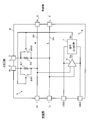
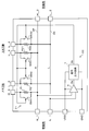
- FIG. 1 is a diagram schematically showing the configuration of the ringing suppression circuit according to the first embodiment.
- FIG. 2 is a diagram schematically showing the configuration of the communication network.
- FIG. 3 is a timing chart schematically showing signal waveforms and operation states of the respective parts.
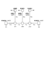
- FIG. 4 is a diagram schematically showing a communication network model used for simulation of circuit operation.
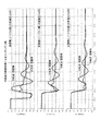
- FIG. 5 is a diagram showing a simulation result of the circuit operation.
- FIG. 6 is a diagram schematically showing the configuration of the ringing suppression circuit according to the second embodiment.
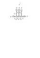
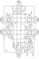
- FIG. 7 is a diagram schematically showing the configuration of the ringing suppression circuit according to the third embodiment.
- a communication network 1 shown in FIG. 2 includes a transmission line 3 configured by twisted pair wires for control communication between a plurality of communication nodes 2 (hereinafter simply referred to as nodes 2) mounted on a vehicle. It is a network connected via Each node 2 is an electronic control device that controls the actuator based on sensors and information from the sensors for detecting the state of the vehicle.
- Each node 2 is provided with a communication circuit (not shown), which converts transmission data and reception data into a communication signal according to a communication protocol on the transmission line 3, such as a CAN protocol, and communicates with other nodes 2. .
- a branch connector 4 corresponding to a branch point that branches the transmission line 3 is provided in the middle of the transmission line 3 as appropriate.
- two nodes 2 indicated as “T” in a rectangle indicate nodes with termination resistors, and other nodes 2 indicate nodes without termination resistors.
- the transmission line 3 between the nodes with termination resistors is called a “trunk line”, and the other transmission lines 3 are called “stubs”.
- the ringing suppression circuit 5 shown in FIG. 1 is provided in the branch connector 4 that branches the transmission line 3 as shown in FIG. 2 that branches the transmission line 3 from the trunk line to one node 2 that does not have a termination resistor. It is done.
- Terminals H_1, L_1, H_2, and L_2 are connection terminals that connect the transmission line 3 on the main line side.
- Terminals H_3 and L_3 are connection terminals for connecting the transmission line 3 on the stub side.
- a high potential side signal line 3P (hereinafter abbreviated as signal line 3P) is connected between the terminals H_1 and H_2, and a low potential side signal line is connected between the terminals L_1 and L_2.
- 3N (hereinafter abbreviated as signal line 3N) is connected.
- the comparator 6 detects the signal level of the differential signal transmitted through the transmission line 3, that is, the communication bus, and corresponds to a detection circuit. Each input terminal of the comparator 6 is connected to the signal lines 3P and 3N, respectively.
- the comparator 6 and the signal output circuit 7 are supplied with a power supply voltage (for example, 5 V) via the power supply terminal VDD and the ground terminal GND.
- the comparator 6 outputs a high level (for example, 5V) signal when the difference voltage between the signal lines 3P and 3N is a voltage (for example, 0V) representing a recessive.
- the comparator 6 outputs a low level (eg, 0 V) signal when the difference voltage between the signal lines 3P and 3N is a voltage representing a dominant (eg, 2 V or more). That is, the output signal Sa of the comparator 6 is high when the signal level of the differential signal, that is, the level representing the recessive level of the communication bus, and low when the level of the communication bus represents the dominant level.
- the output signal Sa of the comparator 6 is given to the signal output circuit 7.
- the signal output circuit 7 is configured as a one-shot multi-output circuit, and outputs a switching signal Sb that becomes a high level only for a certain period when the output signal Sa of the comparator 6 changes from a low level to a high level. That is, the signal output circuit 7 outputs the switching signal Sb that is at a high level for a certain period when it is detected that the communication bus has changed from dominant to recessive.
- the high level corresponds to the first level
- the low level corresponds to the second level.
- a parallel circuit of a resistor R1 and a switch SW1 is connected between the signal line 3P and the terminal H_3.
- a parallel circuit of a resistor R2 and a switch SW2 is connected between the signal line 3N and the terminal L_3.
- the switches SW1 and SW2 are constituted by semiconductor switching elements such as MOS transistors, for example, and their on / off is controlled by a switching signal Sb output from the signal output circuit 7.
- the resistors R1 and R2 correspond to impedance elements for impedance matching on the stub side, and the resistance values are set according to the characteristic impedance of the transmission line 3, the length of the transmission line 3, and the like.
- the switches SW1 and SW2 correspond to switches that open and close both ends of the impedance element.
- the switches SW1 and SW2 are turned on when the switching signal Sb is at a low level, and are turned off when the switching signal Sb is at a high level.
- a connection state a state in which the resistors R1 and R2 are interposed in series in the path on the stub side for a certain period (hereinafter referred to as a connection state). Called).
- both ends of the resistors R1 and R2 are short-circuited by the switches SW1 and SW2, that is, the resistors R1 and R2 are not interposed in the path on the stub side (hereinafter, not connected). Called a state).
- the switch 8 is configured by the switches SW 1 and SW 2, the comparator 6, and the signal output circuit 7.
- the operation of the ringing suppression circuit 5 configured as described above will be described with reference to the timing chart of FIG.
- the difference voltage Vdiff between the signal lines 3P and 3N changes from the level representing dominant to the level representing recessive
- the output signal Sa of the comparator 6 changes from the low level to the high level.
- the switching signal Sb output from the signal output circuit 7 changes from the low level to the high level, and thereafter, the high level is maintained for a certain period.
- the switches SW1 and SW2 are turned off (OPEN) for a certain period when the switching signal Sb is at a high level. For this reason, the resistors R1 and R2 are connected in series in the stub side path, and impedance matching on the stub side is achieved. During a period excluding such a certain period, that is, a period in which the switching signal Sb is at a low level, the switches SW1 and SW2 are turned on (CLOSE). Therefore, both ends of the resistors R1 and R2 are short-circuited, that is, a “non-connected state” in which the resistors R1 and R2 are not interposed in the path on the stub side. In this case, the transmission line 3 on the stub side is in the same state as usual, and the differential signal is not attenuated.
- FIG. 4 the communication network model shown in FIG. 4 is used.
- three branch connectors JC1 to JC3 are provided between nodes N1 and N2 having a terminal resistance of 120 ⁇ .
- the branch connectors JC1 and JC2 and the branch connectors JC2 and JC3 are each connected by a 1 m transmission line.
- the branch connector JC1 is connected to the node N1 and the node N3 not provided with a termination resistor by 4 m transmission lines.
- the branch connector JC2 and the node N4 that does not include a termination resistor are connected by a 4 m transmission line.
- the branch connector JC3 is connected to the node N2 and the node N5 that does not include a termination resistor by a 4 m transmission line.
- the waveform of the differential voltage of the transmission line 3 when the ringing suppression circuit 5 is provided in all of the branch connectors JC1 to JC3 and when the ringing suppression circuit 5 is not provided in all of the branch connectors JC1 to JC3 are shown in FIG.
- the waveform is as shown in FIG.
- the node N3 is a transmitting node
- the nodes N4 and N5 are receiving nodes.
- the ringing suppression circuit 5 when the ringing suppression circuit 5 is provided in the branch connectors JC1 to JC3, the oscillation of the voltage waveform after the transition of the communication bus from dominant to recessive is smaller and faster than when the ringing suppression circuit 5 is not provided. It has converged. That is, from the result of this simulation, it can be seen that the ringing suppression circuit 5 of the present embodiment is provided in the branch connectors JC1 to JC3, thereby suppressing ringing that occurs with the transmission of the differential signal.
- a ringing suppression circuit 5 is provided in the branch connector 4 of the transmission line 3.
- the resistors R1 and R2 are connected in series to the stub side path for a certain period.
- the resistors R1 and R2 which are impedance elements, are interposed in series in the path on the stub side. Ringing due to side reflection noise is suppressed.
- the resistors R1 and R2 are not connected to the stub side path during a period other than the predetermined period. In this way, when ringing is difficult to occur, such as when the signal level of the differential signal is dominant, the impedance element does not intervene in the path on the stub side, so the differential signal passing through the path is not attenuated. Communication stability is not reduced. Therefore, according to the present embodiment, it is possible to suppress ringing caused by reflection in the stub formed by branching while maintaining good communication stability.
- the switching unit 8 has a relatively simple circuit configuration that switches between “connected state” and “non-connected state” by turning on and off the switches SW1 and SW2 that open and close both ends of the resistors R1 and R2. Therefore, according to the present embodiment, the above-described effects can be obtained without causing a significant increase in circuit scale.
- the switching unit 8 receives a comparator 8 that detects that the communication bus has changed from dominant to recessive, and a switching signal Sb that becomes a high level for a certain period when the output signal Sa of the comparator 8 changes from a low level to a high level.
- the signal output circuit 7 for output is provided. Then, the switches SW1 and SW2 are turned on / off by the switching signal Sb, thereby switching between the “connected state” and the “non-connected state”.
- the period during which the ringing is suppressed can be changed as appropriate by setting a certain period in the signal output circuit 7.
- the ringing suppression circuit 21 of this embodiment shown in FIG. 6 is provided at a branch point that branches the transmission line 3 from the main line to two nodes 2 that do not have a termination resistor.
- the ringing suppression circuit 21 includes resistors R21 and R22 and switches SW21 and SW22 corresponding to impedance elements added to the ringing suppression circuit 5 of the first embodiment.
- the terminals H_4 and L_4 are connection terminals that connect the transmission line 3 on the stub side, like the terminals H_3 and L_3.
- a parallel circuit of a resistor R21 and a switch SW21 is connected between the signal line 3P and the terminal H_4.
- a parallel circuit of a resistor R22 and a switch SW22 is connected between the signal line 3N and the terminal L_4.
- ON / OFF of the switches SW21 and SW22 is controlled by a switching signal Sb output from the signal output circuit 7.
- the switching unit 22 is configured by the switches SW1, SW2, SW21, SW22, the comparator 6 and the signal output circuit 7.
- the ringing suppression circuit 21 of the present embodiment is suitable for an application provided at such a branch point.
- the configuration of the present embodiment is a configuration corresponding to the case where the number of branches is “2”. However, when the number of branches is “3” or more, the impedance elements and switches corresponding to the corresponding number are used. May be provided in the path on the stub side.
- the third embodiment will be described below with reference to FIG.
- the ringing suppression circuit 31 of this embodiment shown in FIG. 7 is provided at a star-shaped branch point among the branch points that branch the transmission line 3.
- the terminals H_31, L_31, H_32, L_32, H_33, L_33, H_34, L_34, H_35, L_35, H_36, and L_36 are all connection terminals that connect the transmission line 3 on the stub side.
- a parallel circuit of a resistor R31 and a switch SW31 is connected between the signal line 3P for transmitting the differential signal and the terminal H_31, and a resistor R32 is connected between the signal line 3N for transmitting the differential signal and the terminal L_31. And the parallel circuit of switch SW32 is connected.
- a parallel circuit of a resistor R33 and a switch SW33 is connected between the signal line 3P and the terminal H_32, and a parallel circuit of a resistor R34 and a switch SW34 is connected between the signal line 3N and the terminal L_32.
- a parallel circuit of a resistor R35 and a switch SW35 is connected between the signal line 3P and the terminal H_33, and a parallel circuit of a resistor R36 and a switch SW36 is connected between the signal line 3N and the terminal L_33.
- a parallel circuit of a resistor R37 and a switch SW37 is connected between the signal line 3P and the terminal H_34, and a parallel circuit of a resistor R38 and a switch SW38 is connected between the signal line 3N and the terminal L_34.
- a parallel circuit of a resistor R39 and a switch SW39 is connected between the signal line 3P and the terminal H_35, and a parallel circuit of a resistor R40 and a switch SW40 is connected between the signal line 3N and the terminal L_35.
- a parallel circuit of a resistor R41 and a switch SW41 is connected between the signal line 3P and the terminal H_36, and a parallel circuit of a resistor R42 and a switch SW42 is connected between the signal line 3N and the terminal L_36.
- the ON / OFF of the switches SW31 to SW42 is controlled by a switching signal Sb output from the signal output circuit 7.
- the resistors R31 to R42 correspond to impedance elements
- the switching unit 32 is configured by the switches SW31 to SW42, the comparator 6, and the signal output circuit 7.
- the ringing suppression circuit 31 of the present embodiment is suitable for an application provided at such a branch point.
- the configuration of the present embodiment is a configuration corresponding to the case where the number of branches is “6” among the star-type branch points, but the number of branches is “5” or less, or “7” or more. In such a case, it is only necessary to provide impedance elements and switches corresponding to the path in the path on the stub side.
- the impedance element for impedance matching on the stub side is not limited to resistance elements such as resistors R1, R2, R21, and R22, and may be, for example, an on-resistance of a MOS transistor.
- the switching units 8, 22, and 32 When detecting that the signal level of the differential signal has changed from dominant to recessive, the switching units 8, 22, and 32 switch to the “connected state” for a certain period, and to the “unconnected state” for a period other than the certain period. Any function can be used as long as the function of switching can be realized, and the specific configuration thereof can be changed as appropriate.
- the communication protocol is not limited to CAN, and any communication protocol that transmits differential signals via a pair of communication lines is applicable.
- the present disclosure has been described with reference to the embodiments, it is understood that the present disclosure is not limited to the embodiments and structures. The present disclosure includes various modifications and modifications within the equivalent range. In addition, various combinations and forms, as well as other combinations and forms including only one element, more or less, are within the scope and spirit of the present disclosure.
Landscapes
- Engineering & Computer Science (AREA)
- Theoretical Computer Science (AREA)
- Computer Networks & Wireless Communication (AREA)
- Signal Processing (AREA)
- Computer Hardware Design (AREA)
- Physics & Mathematics (AREA)
- General Engineering & Computer Science (AREA)
- General Physics & Mathematics (AREA)
- Human Computer Interaction (AREA)
- Computing Systems (AREA)
- Mathematical Physics (AREA)
- Power Engineering (AREA)
- Dc Digital Transmission (AREA)
- Cable Transmission Systems, Equalization Of Radio And Reduction Of Echo (AREA)
- Logic Circuits (AREA)
Abstract
リンギング抑制回路(5、21、31)は、差動信号を伝送する伝送線路(3)を分岐する分岐点(4)に設けられ、前記差動信号の伝送に伴い発生するリンギングを抑制するもので、インピーダンス素子(R1、R2、R21、R22、R31~R42)と、前記インピーダンス素子を分岐によって形成されるスタブ側の経路に直列に介在させる接続状態と、前記インピーダンス素子を前記スタブ側の経路に介在させない非接続状態とを切り替える切替部(8、22、32)とを備える。前記切替部は、前記差動信号の信号レベルがドミナントからレセッシブに変化したことを検出すると一定期間だけ前記接続状態に切り替え、前記一定期間を除く期間には前記非接続状態に切り替える。
Description
本出願は、2016年5月25日に出願された日本出願番号2016-104316号に基づくもので、ここにその記載内容を援用する。
本開示は、差動信号を伝送する伝送線路を分岐する分岐点に設けられ、その差動信号の伝送に伴い発生するリンギングを抑制するリンギング抑制回路に関する。
一対の通信線からなる伝送線路を介してデジタル信号を伝送する場合、受信側においては、信号レベルが変化するタイミングで信号エネルギーの一部が反射することで、オーバーシュートやアンダーシュートのような波形の歪み、すなわちリンギングが生じる問題がある。従来、このような波形歪みを抑制するため、様々な技術が提案されている。
例えば、上記伝送線路を分岐する分岐点でのリンギング抑制やリンギング防止の技術として、特許文献1、2に記載の技術を挙げることができる。特許文献1には、バス分岐点での反射ノイズを低減するために、メインバスとスタブバスとの間にインピーダンスを変更可能なMOSトランジスタを介在させた構成のインピーダンス整合回路を設けることが記載されている。また、特許文献2には、バス分岐点での反射ノイズの周波数低域の信号を減衰させる抵抗およびコイルの並列回路からなるフィルタ回路を設けることが記載されている。
インピーダンス整合回路を設ける従来技術では、接続点におけるインピーダンス整合が送信時または受信時にて行われるため、車載LANの一つであるCAN通信のようなバスの状態による反射ノイズを低減することはできない。また、抵抗およびコイルの並列回路からなるフィルタ回路を設ける従来技術では、特に通信速度と反射ノイズの周波数が近くなるような高速通信において、本来減衰させてはならない通信時の信号をも減衰させてしまうため、結果的に通信安定性が低下するおそれがある。
本開示の目的は、通信安定性を良好に維持しつつ、分岐によって形成されるスタブ内の反射により生じるリンギングを抑制することができるリンギング抑制回路を提供することにある。
本開示の第一の態様において、リンギング抑制回路は、差動信号を伝送する伝送線路を分岐する分岐点に設けられ、差動信号の伝送に伴い発生するリンギングを抑制するもので、インピーダンス素子および切替部を備える。切替部は、インピーダンス素子を分岐によって形成されるスタブ側の経路に直列に介在させる接続状態と、インピーダンス素子をスタブ側の経路に介在させない非接続状態とを切り替える。そして、切替部は、差動信号の信号レベルがドミナントからレセッシブに変化したことを検出すると一定期間だけ接続状態に切り替え、その一定期間を除く期間には非接続状態に切り替える。
このような構成によれば、差動信号の信号レベルがドミナントからレセッシブに変化したとき、つまりリンギングが生じ得るときには、スタブ側の経路に直列にインピーダンス素子が介在することで、スタブ側の反射ノイズによるリンギングが抑制される。また、差動信号の信号レベルがドミナントのときなど、リンギングが生じ難いときには、スタブ側の経路にインピーダンス素子が介在しないため、その経路を通過する差動信号を減衰させることはなく、通信安定性が低下することがない。したがって、上記構成によれば、通信安定性を良好に維持しつつ、分岐によって形成されるスタブ内の反射により生じるリンギングを抑制することができる。
本開示についての上記目的およびその他の目的、特徴や利点は、添付の図面を参照しながら下記の詳細な記述により、より明確になる。その図面は、
図1は、第1実施形態に係るリンギング抑制回路の構成を模式的に示す図であり、
図2は、通信ネットワークの構成を模式的に示す図であり、
図3は、各部の信号波形および動作状態を模式的に示すタイミングチャートであり、
図4は、回路動作のシミュレーションに用いた通信ネットワークモデルを模式的に示す図であり、
図5は、回路動作のシミュレーション結果を示す図であり、
図6は、第2実施形態に係るリンギング抑制回路の構成を模式的に示す図であり、
図7は、第3実施形態に係るリンギング抑制回路の構成を模式的に示す図である。
以下、複数の実施形態について図面を参照して説明する。なお、各実施形態において実質的に同一の構成には同一の符号を付して説明を省略する。
(第1実施形態)
以下、第1実施形態について図1~図5を参照して説明する。
(第1実施形態)
以下、第1実施形態について図1~図5を参照して説明する。
図2に示す通信ネットワーク1は、車両に搭載される複数の通信ノード2(以下、単にノード2と呼ぶ)間の制御通信のために、それらのノード2がツイストペア線で構成される伝送線路3を介して接続されたネットワークである。各ノード2は、それぞれ車両の状態を検出するためのセンサ類やセンサからの情報に基づいてアクチュエータをコントロールする電子制御装置である。
各ノード2には、それぞれ図示しない通信回路が設けられており、伝送線路3での通信プロトコル、例えばCANプロトコルに従って送信データや受信データを通信信号に変換し、他のノード2との通信を行う。伝送線路3の途中には、適宜、伝送線路3を分岐する分岐点に相当する分岐コネクタ4が設けられている。なお、図2において、長方形内に「T」と記載した2つのノード2は、終端抵抗付きのノードを示し、それら以外のノード2は、終端抵抗無しのノードを示している。そして、本明細書では、終端抵抗付きのノード間の伝送線路3を「幹線」と呼び、それ以外の伝送線路3を「スタブ」と呼ぶ。
図1に示すリンギング抑制回路5は、図2に示すような伝送線路3を分岐する分岐コネクタ4のうち、幹線から終端抵抗を備えない1つのノード2へと伝送線路3を分岐するものに設けられる。端子H_1、L_1、H_2、L_2は、幹線側の伝送線路3を接続する接続端子である。また、端子H_3、L_3は、スタブ側の伝送線路3を接続する接続端子である。分岐コネクタ4の内部において、端子H_1、H_2の間には、高電位側信号線3P(以下、信号線3Pと省略する)が接続され、端子L_1、L_2の間には、低電位側信号線3N(以下、信号線3Nと省略する)が接続されている。
コンパレータ6は、伝送線路3、つまり通信バスを介して伝送される差動信号の信号レベルを検出するもので、検出回路に相当する。コンパレータ6の各入力端子は、それぞれ信号線3P、3Nに接続されている。また、コンパレータ6および信号出力回路7には、電源端子VDDおよびグランド端子GNDを介して電源電圧(例えば5V)が供給されている。
コンパレータ6は、信号線3P、3N間の差電圧がレセッシブを表す電圧(例えば0V)であるとき、ハイレベル(例えば5V)の信号を出力する。また、コンパレータ6は、信号線3P、3N間の差電圧がドミナントを表す電圧(例えば2V以上)であるとき、ロウレベル(例えば0V)の信号を出力する。つまり、コンパレータ6の出力信号Saは、差動信号の信号レベル、つまり通信バスがレセッシブを表すレベルのときにハイレベルとなり、通信バスがドミナントを表すレベルのときにロウレベルとなる。コンパレータ6の出力信号Saは、信号出力回路7に与えられている。
信号出力回路7は、ワンショットマルチ出力回路として構成されており、コンパレータ6の出力信号Saがロウレベルからハイレベルに変化すると一定期間だけハイレベルとなる切替信号Sbを出力する。つまり、信号出力回路7は、通信バスがドミナントからレセッシブに変化したことが検出されると一定期間だけハイレベルとなる切替信号Sbを出力する。なお、この場合、ハイレベルが第1レベルに相当し、ロウレベルが第2レベルに相当する。
信号線3Pと端子H_3の間には、抵抗R1およびスイッチSW1の並列回路が接続されている。信号線3Nと端子L_3の間には、抵抗R2およびスイッチSW2の並列回路が接続されている。スイッチSW1、SW2は、例えばMOSトランジスタなどの半導体スイッチング素子により構成されており、そのオンオフは信号出力回路7から出力される切替信号Sbにより制御される。
なお、抵抗R1、R2は、スタブ側のインピーダンス整合を図るためのインピーダンス素子に相当し、その抵抗値は、伝送線路3の特性インピーダンスや伝送線路3の長さなどに応じて設定されている。また、スイッチSW1、SW2はインピーダンス素子の両端を開閉するスイッチに相当する。
スイッチSW1、SW2は、切替信号Sbがロウレベルのときにオンされ、切替信号Sbがハイレベルのときにオフされる。このような構成によれば、コンパレータ6により通信バスがドミナントからレセッシブに変化したことが検出されると、一定期間だけ抵抗R1、R2がスタブ側の経路に直列に介在する状態(以下、接続状態と呼ぶ)になる。そして、上記一定期間を除く期間には、抵抗R1、R2の両端がスイッチSW1、SW2によりショート(短絡)された状態、つまり抵抗R1、R2がスタブ側の経路に介在しない状態(以下、非接続状態と呼ぶ)になる。このような構成において、スイッチSW1、SW2、コンパレータ6および信号出力回路7により、切替部8が構成される。
次に、上記構成のリンギング抑制回路5の動作について、図3のタイミングチャートに沿って説明する。図3に示すように、信号線3P、3N間の差電圧Vdiffがドミナントを表すレベルからレセッシブを表すレベルに変化した時点で、コンパレータ6の出力信号Saがロウレベルからハイレベルに転じる。また、これに伴い、信号出力回路7から出力される切替信号Sbがロウレベルからハイレベルに転じ、その後一定期間だけハイレベルが保持される。
切替信号Sbがハイレベルである一定期間、スイッチSW1、SW2はオフ(OPEN)となる。そのため、抵抗R1、R2がスタブ側の経路に直列に介在する「接続状態」となり、スタブ側のインピーダンス整合が図られる。このような一定期間を除く期間、つまり切替信号Sbがロウレベルである期間、スイッチSW1、SW2はオン(CLOSE)となる。そのため、抵抗R1、R2の両端がショートされた状態、つまり抵抗R1、R2がスタブ側の経路に介在しない「非接続状態」となる。この場合、スタブ側の伝送線路3は通常と同様の状態であり、差動信号が減衰することはない。
続いて、このようなリンギング抑制回路5の回路動作をシミュレーションした結果について図4および図5を参照して説明する。本シミュレーションでは、図4に示した通信ネットワークモデルを使用している。この場合、例えば120Ωの終端抵抗を備えたノードN1、N2間に、3つの分岐コネクタJC1~JC3が設けられている。分岐コネクタJC1、JC2の間と、分岐コネクタJC2、JC3の間とは、それぞれ1mの伝送線路で接続されている。
分岐コネクタJC1と、ノードN1および終端抵抗を備えないノードN3との間は、それぞれ4mの伝送線路で接続されている。分岐コネクタJC2と、終端抵抗を備えないノードN4との間は、4mの伝送線路で接続されている。分岐コネクタJC3と、ノードN2および終端抵抗を備えないノードN5との間は、それぞれ4mの伝送線路で接続されている。
ここで、分岐コネクタJC1~JC3の全てにリンギング抑制回路5を設けた場合と、分岐コネクタJC1~JC3の全てにリンギング抑制回路5を設けない場合とにおける伝送線路3の差電圧の波形は図5に示すような波形となる。なお、この場合、ノードN3が送信側のノードであり、ノードN4、N5が受信側のノードである。
図5に示すように、分岐コネクタJC1~JC3にリンギング抑制回路5を設けた場合のほうが、設けない場合に比べ、通信バスがドミナントからレセッシブに移行した後の電圧波形の振動が小さく且つより早く収束している。つまり、本シミュレーションの結果から、本実施形態のリンギング抑制回路5を分岐コネクタJC1~JC3に設けることにより、差動信号の伝送に伴い発生するリンギングが抑制されることが分かる。
以上説明した本実施形態によれば、次のような効果が得られる。
本実施形態では、伝送線路3の分岐コネクタ4にリンギング抑制回路5が設けられている。そして、リンギング抑制回路5では、通信バスがドミナントからレセッシブに変化したことが検出されると一定期間だけ抵抗R1、R2がスタブ側の経路に直列に介在する接続状態となる。このようにすれば、差動信号の信号レベルがドミナントからレセッシブに変化したとき、つまりリンギングが生じ得るときには、スタブ側の経路に直列にインピーダンス素子である抵抗R1、R2が介在することで、スタブ側の反射ノイズによるリンギングが抑制される。
本実施形態では、伝送線路3の分岐コネクタ4にリンギング抑制回路5が設けられている。そして、リンギング抑制回路5では、通信バスがドミナントからレセッシブに変化したことが検出されると一定期間だけ抵抗R1、R2がスタブ側の経路に直列に介在する接続状態となる。このようにすれば、差動信号の信号レベルがドミナントからレセッシブに変化したとき、つまりリンギングが生じ得るときには、スタブ側の経路に直列にインピーダンス素子である抵抗R1、R2が介在することで、スタブ側の反射ノイズによるリンギングが抑制される。
また、リンギング抑制回路5では、上記一定期間を除く期間には、抵抗R1、R2がスタブ側の経路に介在しない非接続状態となる。このようにすれば、差動信号の信号レベルがドミナントのときなど、リンギングが生じ難いときには、スタブ側の経路にインピーダンス素子が介在しないため、その経路を通過する差動信号を減衰させることはなく、通信安定性が低下することがない。したがって、本実施形態によれば、通信安定性を良好に維持しつつ、分岐によって形成されるスタブ内の反射により生じるリンギングを抑制することができる。
切替部8は、抵抗R1、R2の両端を開閉するスイッチSW1、SW2のオンオフにより「接続状態」および「非接続状態」の切り替えを行うという比較的簡単な回路構成となっている。したがって、本実施形態によれば、大幅な回路規模の増加を招くことなく、上述したような効果を得ることができる。
また、切替部8は、通信バスがドミナントからレセッシブに変化したことを検出するコンパレータ8と、そのコンパレータ8の出力信号Saがロウレベルからハイレベルに転じると一定期間だけハイレベルとなる切替信号Sbを出力する信号出力回路7とを備えた構成となっている。そして、切替信号SbによりスイッチSW1、SW2がオンオフされることで、「接続状態」および「非接続状態」の切り替えが行われる。
このような構成によれば、通信バスがドミナントからレセッシブに変化した際に生じるリンギングの発生を確実に抑制することができる。さらに、そのリンギングを抑制する期間については、信号出力回路7における一定期間の設定により、適宜変更することが可能となる。
(第2実施形態)
以下、第2実施形態について図6を参照して説明する。
図6に示す本実施形態のリンギング抑制回路21は、幹線から終端抵抗を備えない2つのノード2へと伝送線路3を分岐する分岐点に設けられる。
以下、第2実施形態について図6を参照して説明する。
図6に示す本実施形態のリンギング抑制回路21は、幹線から終端抵抗を備えない2つのノード2へと伝送線路3を分岐する分岐点に設けられる。
図6に示すように、リンギング抑制回路21は、第1実施形態のリンギング抑制回路5に対し、インピーダンス素子に相当する抵抗R21、R22およびスイッチSW21、SW22が追加されている。この場合、端子H_4、L_4は、端子H_3、L_3と同様、スタブ側の伝送線路3を接続する接続端子である。
信号線3Pと端子H_4の間には、抵抗R21およびスイッチSW21の並列回路が接続されている。信号線3Nと端子L_4の間には、抵抗R22およびスイッチSW22の並列回路が接続されている。スイッチSW21、SW22のオンオフは、信号出力回路7から出力される切替信号Sbにより制御される。なお、この場合、スイッチSW1、SW2、SW21、SW22、コンパレータ6および信号出力回路7により、切替部22が構成される。
伝送線路3を分岐する分岐点としては、幹線から終端抵抗を備えない複数のノード2へと伝送線路3を分岐するものも存在する。本実施形態のリンギング抑制回路21は、このような分岐点に設ける用途として好適である。なお、本実施形態の構成は、分岐数が「2」の場合に対応した構成となっているが、分岐数が「3」以上である場合には、それに対応した分だけのインピーダンス素子およびスイッチをスタブ側の経路に設ければよい。
(第3実施形態)
以下、第3実施形態について図7を参照して説明する。
図7に示す本実施形態のリンギング抑制回路31は、伝送線路3を分岐する分岐点のうち、スター型の分岐点に設けられる。この場合、端子H_31、L_31、H_32、L_32、H_33、L_33、H_34、L_34、H_35、L_35、H_36、L_36は、いずれもスタブ側の伝送線路3を接続する接続端子である。
以下、第3実施形態について図7を参照して説明する。
図7に示す本実施形態のリンギング抑制回路31は、伝送線路3を分岐する分岐点のうち、スター型の分岐点に設けられる。この場合、端子H_31、L_31、H_32、L_32、H_33、L_33、H_34、L_34、H_35、L_35、H_36、L_36は、いずれもスタブ側の伝送線路3を接続する接続端子である。
差動信号を伝送するための信号線3Pと端子H_31の間には抵抗R31およびスイッチSW31の並列回路が接続され、差動信号を伝送するための信号線3Nと端子L_31の間には抵抗R32およびスイッチSW32の並列回路が接続されている。信号線3Pと端子H_32の間には抵抗R33およびスイッチSW33の並列回路が接続され、信号線3Nと端子L_32の間には抵抗R34およびスイッチSW34の並列回路が接続されている。
信号線3Pと端子H_33の間には抵抗R35およびスイッチSW35の並列回路が接続され、信号線3Nと端子L_33の間には抵抗R36およびスイッチSW36の並列回路が接続されている。信号線3Pと端子H_34の間には抵抗R37およびスイッチSW37の並列回路が接続され、信号線3Nと端子L_34の間には抵抗R38およびスイッチSW38の並列回路が接続されている。
信号線3Pと端子H_35の間には抵抗R39およびスイッチSW39の並列回路が接続され、信号線3Nと端子L_35の間には抵抗R40およびスイッチSW40の並列回路が接続されている。信号線3Pと端子H_36の間には抵抗R41およびスイッチSW41の並列回路が接続され、信号線3Nと端子L_36の間には抵抗R42およびスイッチSW42の並列回路が接続されている。
スイッチSW31~SW42のオンオフは、信号出力回路7から出力される切替信号Sbにおり制御される。なお、この場合、抵抗R31~R42がインピーダンス素子に相当し、スイッチSW31~SW42、コンパレータ6および信号出力回路7により切替部32が構成される。
伝送線路3を分岐する分岐点としては、スター型の分岐点も存在する。本実施形態のリンギング抑制回路31は、このような分岐点に設ける用途として好適である。なお、本実施形態の構成は、スター型の分岐点のうち分岐数が「6」の場合に対応した構成となっているが、分岐数が「5」以下の場合や「7」以上である場合には、それに対応した分だけのインピーダンス素子およびスイッチをスタブ側の経路に設ければよい。
(その他の実施形態)
なお、本開示は上記し且つ図面に記載した各実施形態に限定されるものではなく、その要旨を逸脱しない範囲で任意に変形、組み合わせ、あるいは拡張することができる。
なお、本開示は上記し且つ図面に記載した各実施形態に限定されるものではなく、その要旨を逸脱しない範囲で任意に変形、組み合わせ、あるいは拡張することができる。
スタブ側のインピーダンス整合を図るためのインピーダンス素子としては、抵抗R1、R2、R21、R22などの抵抗素子に限らずともよく、例えばMOSトランジスタのオン抵抗であってもよい。
切替部8、22、32としては、差動信号の信号レベルがドミナントからレセッシブに変化したことを検出すると一定期間だけ「接続状態」に切り替え、一定期間を除く期間には「非接続状態」に切り替える、という機能を実現できるものであればよく、その具体的な構成などは適宜変更可能である。
通信プロトコルはCANに限ることなく、一対の通信線を介して差動信号を伝送する通信プロトコルであれば適用が可能である。
本開示は、実施例に準拠して記述されたが、本開示は当該実施例や構造に限定されるものではないと理解される。本開示は、様々な変形例や均等範囲内の変形をも包含する。加えて、様々な組み合わせや形態、さらには、それらに一要素のみ、それ以上、あるいはそれ以下、を含む他の組み合わせや形態をも、本開示の範疇や思想範囲に入るものである。
本開示は、実施例に準拠して記述されたが、本開示は当該実施例や構造に限定されるものではないと理解される。本開示は、様々な変形例や均等範囲内の変形をも包含する。加えて、様々な組み合わせや形態、さらには、それらに一要素のみ、それ以上、あるいはそれ以下、を含む他の組み合わせや形態をも、本開示の範疇や思想範囲に入るものである。
Claims (6)
- 差動信号を伝送する伝送線路(3)を分岐する分岐点(4)に設けられ、前記差動信号の伝送に伴い発生するリンギングを抑制するリンギング抑制回路(5、21、31)であって、
インピーダンス素子(R1、R2、R21、R22、R31~R42)と、
前記インピーダンス素子を分岐によって形成されるスタブ側の経路に直列に介在させる接続状態と、前記インピーダンス素子を前記スタブ側の経路に介在させない非接続状態とを切り替える切替部(8、22、32)と、
を備え、
前記切替部は、前記差動信号の信号レベルがドミナントからレセッシブに変化したことを検出すると一定期間だけ前記接続状態に切り替え、前記一定期間を除く期間には前記非接続状態に切り替えるリンギング抑制回路。 - 前記切替部は、前記インピーダンス素子の両端を開閉するスイッチ(SW1、SW2、SW21、SW22、SW31~SW42)を備え、前記スイッチをオフすることで前記接続状態に切り替え、前記スイッチをオンすることで前記非接続状態に切り替える請求項1に記載のリンギング抑制回路。
- 前記切替部は、前記差動信号の信号レベルを検出する検出回路(6)と、前記検出回路により前記差動信号の信号レベルがドミナントからレセッシブに変化したことが検出されると前記一定期間だけ第1レベルとなる切替信号を出力する信号出力回路(7)と、を備え、前記切替信号が前記第1レベルである期間に前記接続状態に切り替え、前記切替信号が前記第1レベルとは異なる第2レベルである期間に前記非接続状態に切り替える請求項1または2に記載のリンギング抑制回路。
- 前記分岐点は、終端抵抗を備える2つの通信ノード(2)間を接続する幹線から終端抵抗を備えない1つの通信ノード(2)へと前記伝送線路を分岐するものであり、
前記インピーダンス素子および前記切替部は、前記分岐点から前記終端抵抗を備えない1つの通信ノード(2)へと至る経路に対応して設けられる請求項1から3のいずれか一項に記載のリンギング抑制回路。 - 前記分岐点は、終端抵抗を備える2つの通信ノード(2)間を接続する幹線から終端抵抗を備えない複数の通信ノード(2)へと前記伝送線路を分岐するものであり、
前記インピーダンス素子および前記切替部は、前記分岐点から前記終端抵抗を備えない複数の通信ノード(2)のそれぞれへと至る経路に対応して設けられる請求項1から3のいずれか一項に記載のリンギング抑制回路。 - 前記分岐点は、スター型の分岐点であり、
前記インピーダンス素子および前記切替部は、前記分岐点から前記分岐点に接続される複数の通信ノード(2)のそれぞれへと至る経路に対応して設けられる請求項1から3のいずれか一項に記載のリンギング抑制回路。
Applications Claiming Priority (2)
| Application Number | Priority Date | Filing Date | Title |
|---|---|---|---|
| JP2016104316A JP6520824B2 (ja) | 2016-05-25 | 2016-05-25 | リンギング抑制回路 |
| JP2016-104316 | 2016-05-25 |
Publications (1)
| Publication Number | Publication Date |
|---|---|
| WO2017203840A1 true WO2017203840A1 (ja) | 2017-11-30 |
Family
ID=60411315
Family Applications (1)
| Application Number | Title | Priority Date | Filing Date |
|---|---|---|---|
| PCT/JP2017/013941 Ceased WO2017203840A1 (ja) | 2016-05-25 | 2017-04-03 | リンギング抑制回路 |
Country Status (2)
| Country | Link |
|---|---|
| JP (1) | JP6520824B2 (ja) |
| WO (1) | WO2017203840A1 (ja) |
Citations (3)
| Publication number | Priority date | Publication date | Assignee | Title |
|---|---|---|---|---|
| JP2007166109A (ja) * | 2005-12-12 | 2007-06-28 | Matsushita Electric Works Ltd | 伝送システムの分岐器並びに伝送システム |
| JP2009253498A (ja) * | 2008-04-03 | 2009-10-29 | Toyota Motor Corp | 通信装置 |
| JP2014011776A (ja) * | 2012-07-03 | 2014-01-20 | Nippon Soken Inc | 受信装置 |
-
2016
- 2016-05-25 JP JP2016104316A patent/JP6520824B2/ja not_active Expired - Fee Related
-
2017
- 2017-04-03 WO PCT/JP2017/013941 patent/WO2017203840A1/ja not_active Ceased
Patent Citations (3)
| Publication number | Priority date | Publication date | Assignee | Title |
|---|---|---|---|---|
| JP2007166109A (ja) * | 2005-12-12 | 2007-06-28 | Matsushita Electric Works Ltd | 伝送システムの分岐器並びに伝送システム |
| JP2009253498A (ja) * | 2008-04-03 | 2009-10-29 | Toyota Motor Corp | 通信装置 |
| JP2014011776A (ja) * | 2012-07-03 | 2014-01-20 | Nippon Soken Inc | 受信装置 |
Also Published As
| Publication number | Publication date |
|---|---|
| JP6520824B2 (ja) | 2019-05-29 |
| JP2017212584A (ja) | 2017-11-30 |
Similar Documents
| Publication | Publication Date | Title |
|---|---|---|
| US10530612B2 (en) | Subscriber station for a bus system and method for reducing line-related emissions in a bus system | |
| CN102273155B (zh) | 数据传输系统 | |
| JP5897038B2 (ja) | プリエンファシスを備えた電圧モードドライバ | |
| US7042254B2 (en) | Differential signal receiving device and differential signal transmission system | |
| CN107276869B (zh) | 电子设备、用于数据传输的方法和电子系统 | |
| US20040043739A1 (en) | Controller area network transceiver having capacitive balancing circuit for improved receiver common-mode refection | |
| JP5543402B2 (ja) | リンギング抑制回路 | |
| KR20100043971A (ko) | 출력신호의 전압 스윙을 조절할 수 있는 출력 회로, 이를 포함하는 반도체 장치, 및 반도체 장치들을 포함하는 통신 시스템 | |
| US8222925B2 (en) | Multimode Ethernet line driver | |
| JP6460049B2 (ja) | リンギング抑制回路 | |
| US10419071B2 (en) | Ringing suppression circuit | |
| WO2018020783A1 (ja) | リンギング抑制回路 | |
| CN105978830A (zh) | 用于通过传输线路传输差分和单端信号的发送与接收电路 | |
| US20140177739A1 (en) | Transmission device and node for the same | |
| US7843281B2 (en) | Circuit topology for multiple loads | |
| CN110489803A (zh) | 一种针对fly-by拓扑结构的优化信号链路以及优化方法 | |
| JP6520824B2 (ja) | リンギング抑制回路 | |
| JP5626240B2 (ja) | ドライバ回路 | |
| CN116918308A (zh) | 延迟信号产生电路、发送电路、电子控制单元和车辆 | |
| US6650144B2 (en) | Line driver for supplying symmetrical output signals to a two-wire communication bus | |
| JP7680526B2 (ja) | 送信回路、電子制御ユニット、及び車両 | |
| US7451356B2 (en) | Apparatus for configuring network media connections | |
| KR20130113034A (ko) | 고속 캔 통신용 버스 장치 | |
| Lee | Dynamic ringing suppression in a CAN-FD transceiver using peak voltage detection and impedance switching | |
| CN116094505A (zh) | 分布式驱动器及方法 |
Legal Events
| Date | Code | Title | Description |
|---|---|---|---|
| NENP | Non-entry into the national phase |
Ref country code: DE |
|
| 121 | Ep: the epo has been informed by wipo that ep was designated in this application |
Ref document number: 17802441 Country of ref document: EP Kind code of ref document: A1 |
|
| 122 | Ep: pct application non-entry in european phase |
Ref document number: 17802441 Country of ref document: EP Kind code of ref document: A1 |