WO2017199641A1 - Electric motor control device and electric vehicle equipped with same - Google Patents
Electric motor control device and electric vehicle equipped with same Download PDFInfo
- Publication number
- WO2017199641A1 WO2017199641A1 PCT/JP2017/014758 JP2017014758W WO2017199641A1 WO 2017199641 A1 WO2017199641 A1 WO 2017199641A1 JP 2017014758 W JP2017014758 W JP 2017014758W WO 2017199641 A1 WO2017199641 A1 WO 2017199641A1
- Authority
- WO
- WIPO (PCT)
- Prior art keywords
- phase
- zero
- pulse width
- control device
- motor
- Prior art date
Links
Images


Classifications
-
- B—PERFORMING OPERATIONS; TRANSPORTING
- B60—VEHICLES IN GENERAL
- B60L—PROPULSION OF ELECTRICALLY-PROPELLED VEHICLES; SUPPLYING ELECTRIC POWER FOR AUXILIARY EQUIPMENT OF ELECTRICALLY-PROPELLED VEHICLES; ELECTRODYNAMIC BRAKE SYSTEMS FOR VEHICLES IN GENERAL; MAGNETIC SUSPENSION OR LEVITATION FOR VEHICLES; MONITORING OPERATING VARIABLES OF ELECTRICALLY-PROPELLED VEHICLES; ELECTRIC SAFETY DEVICES FOR ELECTRICALLY-PROPELLED VEHICLES
- B60L9/00—Electric propulsion with power supply external to the vehicle
- B60L9/16—Electric propulsion with power supply external to the vehicle using ac induction motors
- B60L9/18—Electric propulsion with power supply external to the vehicle using ac induction motors fed from dc supply lines
-
- H—ELECTRICITY
- H02—GENERATION; CONVERSION OR DISTRIBUTION OF ELECTRIC POWER
- H02M—APPARATUS FOR CONVERSION BETWEEN AC AND AC, BETWEEN AC AND DC, OR BETWEEN DC AND DC, AND FOR USE WITH MAINS OR SIMILAR POWER SUPPLY SYSTEMS; CONVERSION OF DC OR AC INPUT POWER INTO SURGE OUTPUT POWER; CONTROL OR REGULATION THEREOF
- H02M7/00—Conversion of ac power input into dc power output; Conversion of dc power input into ac power output
- H02M7/42—Conversion of dc power input into ac power output without possibility of reversal
- H02M7/44—Conversion of dc power input into ac power output without possibility of reversal by static converters
- H02M7/48—Conversion of dc power input into ac power output without possibility of reversal by static converters using discharge tubes with control electrode or semiconductor devices with control electrode
-
- H—ELECTRICITY
- H02—GENERATION; CONVERSION OR DISTRIBUTION OF ELECTRIC POWER
- H02P—CONTROL OR REGULATION OF ELECTRIC MOTORS, ELECTRIC GENERATORS OR DYNAMO-ELECTRIC CONVERTERS; CONTROLLING TRANSFORMERS, REACTORS OR CHOKE COILS
- H02P21/00—Arrangements or methods for the control of electric machines by vector control, e.g. by control of field orientation
- H02P21/22—Current control, e.g. using a current control loop
-
- Y—GENERAL TAGGING OF NEW TECHNOLOGICAL DEVELOPMENTS; GENERAL TAGGING OF CROSS-SECTIONAL TECHNOLOGIES SPANNING OVER SEVERAL SECTIONS OF THE IPC; TECHNICAL SUBJECTS COVERED BY FORMER USPC CROSS-REFERENCE ART COLLECTIONS [XRACs] AND DIGESTS
- Y02—TECHNOLOGIES OR APPLICATIONS FOR MITIGATION OR ADAPTATION AGAINST CLIMATE CHANGE
- Y02T—CLIMATE CHANGE MITIGATION TECHNOLOGIES RELATED TO TRANSPORTATION
- Y02T10/00—Road transport of goods or passengers
- Y02T10/60—Other road transportation technologies with climate change mitigation effect
- Y02T10/72—Electric energy management in electromobility
Definitions
- the present invention relates to a motor control device, and more particularly to a vehicle-mounted motor control device.
- Hybrid vehicles and electric vehicles are required to have improved reliability from the viewpoint of preventing failure during vehicle travel and to improve output torque from the viewpoint of vehicle weight reduction.
- a three-phase six-wire drive device has been considered, but since a motor with no neutral point connected is used, a zero-phase current is superimposed on the drive current that drives the motor, resulting in copper loss. There was a problem that losses such as increased.
- Patent Document 1 JP-A-63-224693.
- Patent Document 1 JP-A-63-224693.
- This publication describes that “a current-carrying mode of the first and second voltage source inverters that reduces the current value of the zero-phase current is selected from a plurality of current-carrying modes”. As a result, the inverter operates so as to reduce the zero-phase current, so that the loss due to the zero-phase current can be reduced.
- An object of the present invention is to reduce the number of times of switching when reducing the zero-phase current.
- a motor control device controls a motor in which windings of each phase are independently connected, and controls a voltage to be applied to the motor based on an input torque command.
- a motor control device that outputs a PWM control signal for the purpose, a pulse width of a zero-phase voltage consisting of the sum of output voltages based on a zero-phase voltage command for reducing the zero-phase current obtained from the AC current of the motor And controlling the amplitude.
- the inverter control device can reduce the number of times of switching when the zero-phase current is reduced.
- FIG. 4 is a diagram illustrating a flowchart of a switching signal generation unit 30.
- FIG. It is a figure which shows the process of step 2 in the flowchart of FIG. 5, and has shown the hexagon part shown with the thick dotted line in the vector diagram of FIG.
- FIG. 5 shows the process of step 4 in the flowchart of FIG. 5, and has shown the hexagon part shown with the thick dotted line in the vector diagram of FIG.
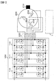
- FIG. 1 is a diagram showing a configuration of a motor drive device according to an embodiment of the present invention.
- the motor driving device includes a motor 200, a position sensor 210, a current sensor 220, an inverter 100, and the inverter control device 1.
- the motor drive device functions as a motor drive system that drives the motor.
- the motor 200 is constituted by an embedded magnet synchronous motor or the like to which a neutral point is not connected.
- the U-phase winding 201 wound around the stator of the motor 200 is connected to the output terminal of the U-phase full bridge inverter 110.
- the V-phase winding 202 wound around the stator of the motor 200 is connected to the output terminal of the V-phase full bridge inverter 111.
- W phase winding 203 wound around the stator of motor 200 is connected to the output terminal of W phase full bridge inverter 112.
- the current flowing in the U-phase winding 201, the V-phase winding 202, and the W-phase winding 203 can be controlled independently.
- the neutral point of the motor 200 since the neutral point of the motor 200 is not connected, the drive current flowing through the U-phase winding 201, the V-phase winding 202, and the W-phase winding 203 is not included in Patent Document 1, as described in Patent Document 1. , Zero phase current is included.
- the position sensor 210 detects the position of the rotor of the motor 200 and outputs the detected rotor position ⁇ .
- the current sensor 220 detects currents flowing in the U-phase winding 201, the V-phase winding 202, and the W-phase winding 203 wound around the stator of the motor 200, and detects the detected three-phase currents iu, iv, iw is output.
- the inverter 100 includes a U-phase full-bridge inverter 110, a V-phase full-bridge inverter 111, and a W-phase full-bridge inverter 112.
- U-phase full-bridge inverter 110, V-phase full-bridge inverter 111, and W-phase full-bridge inverter 112 are connected in parallel to a DC power supply (not shown).
- the U-phase full bridge inverter 110 is composed of switching elements 110a to 110d.
- Switching element 110a is arranged on the U-phase left leg upper arm.
- Switching element 110b is arranged on the U-phase left leg lower arm.
- Switching element 110c is arranged on the U-phase right leg upper arm.
- Switching element 110d is disposed on the U-phase right leg lower arm.
- the V-phase full bridge inverter 111 is composed of switching elements 111a to 111d.
- Switching element 111a is arranged on the V-phase left leg upper arm.
- Switching element 111b is arranged on the lower arm of the V-phase left leg.
- Switching element 111c is arranged on the V-phase right leg upper arm.
- Switching element 111d is arranged on the lower arm of the V-phase right leg.
- the W-phase full bridge inverter 112 is composed of switching elements 112a to 112d.
- Switching element 112a is arranged on the W-phase left leg upper arm.
- Switching element 112b is arranged on the lower arm of the W-phase left leg.
- Switching element 112c is arranged on the W-phase right leg upper arm.
- Switching element 112d is arranged on the lower arm of the W-phase right leg.
- the inverter 100 By turning on or off the switching elements 110a to 110d, the switching elements 111a to 111d, and the switching elements 112a to 112d based on the switching signal generated by the inverter control device 1, the inverter 100 is connected to a DC power supply (not shown).
- the applied DC voltage is converted into an AC voltage.
- the converted AC voltage is applied to the U-phase winding 201, the V-phase winding 202 and the W-phase winding 203 wound around the stator of the motor 200 to generate a three-phase AC current. This three-phase alternating current generates a rotating magnetic field in the motor 200, and the rotor rotates.
- Switching elements 110a to 110d, switching elements 111a to 111d, and switching elements 112a to 112d are configured by combining a metal oxide film type field effect transistor (MOSFET), an insulated gate bipolar transistor (IGBT), and the like with a diode.
- MOSFET metal oxide film type field effect transistor
- IGBT insulated gate bipolar transistor
- the inverter control device 1 performs PWM control on the inverter 100 based on the torque command value T * from the outside, the three-phase currents iu, iv, iw detected by the current sensor 220, and the rotor position ⁇ detected by the position sensor 210. To do.
- FIG. 2 is a diagram showing an example of an output voltage waveform of the motor drive device according to the present embodiment.
- the U phase output voltage Vu is an output voltage of the U phase full bridge inverter 110.
- V-phase output voltage Vv is an output voltage of V-phase full-bridge inverter 111.
- W-phase output voltage Vw is an output voltage of W-phase full-bridge inverter 112.
- the zero-phase output voltage V0 is obtained by the equation (1) from the U-phase output voltage Vu, the V-phase output voltage Vv, and the W-phase output voltage Vw.
- the U-phase full-bridge inverter 110, the V-phase full-bridge inverter 111, and the W-phase full-bridge inverter 112 output either a positive power supply voltage Vdc, a negative power supply voltage ⁇ Vdc, or zero voltage. .
- the amplitude of the zero-phase output voltage V0 is one of the following depending on the combination.
- FIG. 3 is an output voltage vector diagram of the motor drive device according to the present embodiment.
- the components of the output voltage vector are shown in the order of the U phase, the V phase, and the W phase, and the magnitudes are + when the output voltage is a positive power supply voltage Vdc, and negative power supply voltage ⁇
- Vdc positive power supply voltage
- ⁇ negative power supply voltage
- FIG. 4 is a control block diagram for explaining the first embodiment.
- the current command calculation unit 10 calculates the d-axis current command value id * and the q-axis current command value iq * based on the input torque command value T * and the angular velocity ⁇ .
- a method for calculating the d-axis current command value id * and the q-axis current command value iq * there are a maximum torque current control, a field weakening control, and the like. Note that a preset table may be used for calculating the d-axis current command value id * and the q-axis current command value iq *.
- the dq-axis current control unit 20 receives the d-axis current command value id *, the q-axis current command value iq *, the d-axis current detection value id, and the q-axis current detection value iq, and performs proportional control and integral control. Used to output the d-axis voltage command value Vd * and the q-axis voltage command value Vq *.
- the d-axis voltage command value Vd *, the q-axis voltage command value Vq *, and the zero-phase voltage command value V0 * are input to the switching signal generation unit 30, and the switching elements 110a to 110d, the switching elements 111a to 111d, A switching signal for turning on or off the switching elements 112a to 112d is generated.
- the switching signal is input to the inverter 100, and the motor is operated by the above operation.
- the dq converter 40 receives the three-phase currents iu, iv, iw detected by the current sensor 220 and the rotor position ⁇ detected by the position sensor 210, and detects the d-axis current detection value id, the q-axis current detection.
- the value iq is output.
- the zero-phase current calculation unit 50 receives the three-phase currents iu, iv, iw detected by the current sensor 220 and the rotor position ⁇ detected by the position sensor 210, and outputs the zero-phase current i0.
- a formula for calculating the zero-phase current i0 is shown in Formula (3).
- the zero phase current i0 may be calculated in consideration of the zero phase current value estimated from the angular velocity ⁇ .
- the zero-phase current control unit 60 receives the zero-phase current i0 and outputs a zero-phase voltage command value V0 * using proportional control, integral control, or the like.
- the speed converter 70 receives the rotor position ⁇ detected by the position sensor 210 and outputs an angular speed ⁇ .
- FIG. 5 is a diagram showing a flowchart of the switching signal generation unit 30.
- step 1 the switching signal generator 30 determines the polarity of the zero-phase voltage command value V0 * output from the zero-phase voltage controller 60. If the zero-phase voltage command value V0 * is positive, step 2 If the phase voltage command value V0 * is negative, the process of step 9 is performed.
- Step 2 when the zero-phase voltage command value V0 * is positive, the switching signal generator 30 calculates the pulse width of the P1 mode.
- step 3 it is determined whether the pulse width of the P1 mode calculated in step 2 is within the carrier period. If the pulse width of the P1 mode is within the carrier period, the process is completed, and the pulse width of the P1 mode is If the period is exceeded, the process of step 4 is performed.
- step 4 when the pulse width of the P1 mode exceeds the carrier period, the switching signal generation unit 30 calculates the pulse width of the P2 mode.
- step 5 it is determined whether the pulse width of the P2 mode calculated in step 4 is within the carrier period. If the pulse width of the P2 mode is within the carrier period, the process is completed, and the pulse width of the P2 mode is If the period is exceeded, the process of step 6 is performed.
- step 6 when the pulse width of the P2 mode exceeds the carrier period, the switching signal generation unit 30 calculates the pulse width of the P3 mode.
- step 7 it is determined whether the pulse width of the P3 mode calculated in step 6 is within the carrier period. If the pulse width of the P3 mode is within the carrier period, the process is completed, and the pulse width of the P3 mode is equal to the carrier period. If the period is exceeded, the process of step 8 is performed.
- step 8 when the pulse width of the P3 mode exceeds the carrier period, the switching signal generation unit 30 calculates the pulse width of the P4 mode.
- step 9 when the zero-phase voltage command value V0 * is negative, the switching signal generator 30 calculates the pulse width of the N1 mode. Thereafter, in step 10, it is determined whether the pulse width of the N1 mode calculated in step 9 is within the carrier period. If the pulse width of the N1 mode is within the carrier period, the process is completed, and the pulse width of the N1 mode is If the period is exceeded, the process of step 11 is performed.
- step 11 when the pulse width of the N1 mode exceeds the carrier period, the switching signal generation unit 30 calculates the pulse width of the N2 mode.
- step 12 it is determined whether the pulse width of the N2 mode calculated in step 11 is within the carrier period. If the pulse width of the N2 mode is within the carrier period, the process is completed, and the pulse width of the N2 mode is If the period is exceeded, the process of step 13 is performed.
- step 13 when the pulse width of the N2 mode exceeds the carrier period, the switching signal generation unit 30 calculates the pulse width of the N3 mode.
- step 14 it is determined whether the pulse width of the N3 mode calculated in step 13 is within the carrier period. If the pulse width of the N3 mode is within the carrier period, the process is completed, and the pulse width of the N3 mode is equal to the carrier period. If the period is exceeded, the process of step 15 is performed.
- step 15 when the pulse width of the N3 mode exceeds the carrier period, the switching signal generation unit 30 calculates the pulse width of the N4 mode.
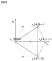
- FIG. 6 is a diagram showing the process of step 2 in the flowchart of FIG. 5, and shows a hexagonal portion indicated by a thick dotted line in the vector diagram of FIG.
- the calculation can be performed by rotating the vector diagram of FIG. 6 by 60 ° and inverting the polarity.
- Va and Vb are voltage command values obtained by converting dq-axis voltage command values Vd * and Vq * into fixed coordinates in FIG.
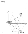
- FIG. 7 is a diagram showing the processing of step 4 in the flowchart of FIG. 5, and shows the hexagonal portion indicated by the thick dotted line in the vector diagram of FIG.
- calculation can be performed by rotating the vector diagram of FIG. 7 by 60 ° and inverting the polarity.
- Va and Vb are voltage command values obtained by converting dq-axis voltage command values Vd * and Vq * into fixed coordinates in FIG.
- FIG. 8 is a diagram showing the processing of step 6 and step 8 in the flowchart of FIG. 5, and shows the hexagonal portion indicated by the thick dotted line in the vector diagram of FIG.
- the calculation can be performed by rotating the vector diagram of FIG. 8 by 60 ° and inverting the polarity.
- Va and Vb are voltage command values obtained by converting dq-axis voltage command values Vd * and Vq * into fixed coordinates in FIG.
- step 8 t1, t2 and t5 are obtained from the dq-axis voltage command values Vd * and Vq * and the zero-phase voltage command value V0 * by the equation (7).
- Va and Vb are voltage command values obtained by converting dq-axis voltage command values Vd * and Vq * into fixed coordinates in FIG.
- FIG. 9 is a diagram showing the processing of step 9 in the flowchart of FIG. 5, and shows the hexagonal portion indicated by the thick dotted line in the vector diagram of FIG.
- calculation can be performed by rotating the vector diagram of FIG. 9 by 60 ° and inverting the polarity.
- Va and Vb are voltage command values obtained by converting the dq-axis voltage command values Vd * and Vq * into fixed coordinates in FIG.
- FIG. 10 is a diagram showing the processing of step 11 in the flowchart of FIG. 5, and shows the hexagonal portion indicated by the thick dotted line in the vector diagram of FIG.
- the calculation can be performed by rotating the vector diagram of FIG. 10 by 60 ° and inverting the polarity.
- Va and Vb are voltage command values obtained by converting the dq axis voltage command values Vd * and Vq * into fixed coordinates in FIG.
- FIG. 11 is a diagram showing the processing of step 13 and step 15 in the flowchart of FIG. 5, and shows the hexagonal portion indicated by the thick dotted line in the vector diagram of FIG.
- the calculation can be performed by rotating the vector diagram of FIG. 11 by 60 ° and inverting the polarity.
- Va and Vb are voltage command values obtained by converting dq-axis voltage command values Vd * and Vq * into fixed coordinates in FIG.
- step 15 t1, t2, and t8 are dq axis voltage command values Vd *, Vq *, It is obtained from the zero-phase voltage command value V0 * by the equation (11).
- Va and Vb are voltage command values obtained by converting dq-axis voltage command values Vd * and Vq * into fixed coordinates in FIG.
- the zero-phase voltage having a small amplitude can be obtained within a range in which the pulse width of the voltage output from the inverter of each phase does not exceed the carrier cycle.
- the switching loss can be reduced by reducing the number of times of switching.
- switching element 112 ... W-phase full bridge inverter, 112a ... switching element, 112b ... switching element, 112c ... switching element, 112d ... switching element , 20 ... Motor, 201 ... U phase winding, 202 ... V phase winding, 203 ... W phase winding, 210 ... Position sensor, 220 ... Current sensor, iu ... U phase current, iv ... V phase current, iw ... W phase Current, id * ... d-axis current command value, iq * ... q-axis current command value, i d ... d-axis current detection value, i q ... q-axis current detection value, i0 ...
Abstract
The purpose of the present invention is to reduce the number of times of switching to be performed when reducing a zero-phase current. This electric motor control device controls an electric motor, the phases of which are connected independently of one another, and has a control means which outputs a PWM control signal for controlling a voltage to be applied to the electric motor on the basis of an input torque command. The control means controls, on the basis of a zero-phase voltage command which is obtained from an alternating current of the electric motor and used for reducing a zero-phase current, the pulse width and amplitude of a zero-phase voltage consisting of the sum of output voltages.
Description
本発明は電動機の制御装置に関し、特に車載用の電動機の制御装置に関する。
The present invention relates to a motor control device, and more particularly to a vehicle-mounted motor control device.
ハイブリッド自動車や電気自動車は、車両走行中の故障発生防止の観点から信頼性の向上と、車両軽量化の観点から出力トルクの向上が要求される。これらの要求に対して三相6線式の駆動装置が考えられているが、中性点が接続されていない電動機を用いるため、電動機を駆動する駆動電流に零相電流が重畳し、銅損などの損失が増加するという課題があった。
Hybrid vehicles and electric vehicles are required to have improved reliability from the viewpoint of preventing failure during vehicle travel and to improve output torque from the viewpoint of vehicle weight reduction. In response to these requirements, a three-phase six-wire drive device has been considered, but since a motor with no neutral point connected is used, a zero-phase current is superimposed on the drive current that drives the motor, resulting in copper loss. There was a problem that losses such as increased.
本技術分野の背景技術として、特開昭63-224693号公報(特許文献1)がある。この公報には、「複数通電モードの中から零相電流の現在値を減少させるような第1および第2の電圧形インバータの通電モードを選択する」と記載されている。これにより零相電流を減少させるようにインバータが動作するため、零相電流による損失を低減することができる。
As background art in this technical field, there is JP-A-63-224693 (Patent Document 1). This publication describes that “a current-carrying mode of the first and second voltage source inverters that reduces the current value of the zero-phase current is selected from a plurality of current-carrying modes”. As a result, the inverter operates so as to reduce the zero-phase current, so that the loss due to the zero-phase current can be reduced.
特許文献1に記載の方法では、零相電流を減少させるためにスイッチング回数が増加する恐れがある。
In the method described in Patent Document 1, there is a possibility that the number of times of switching increases in order to reduce the zero-phase current.
本発明の目的は、零相電流を減少させる際のスイッチング回数を低減することである。
An object of the present invention is to reduce the number of times of switching when reducing the zero-phase current.
上記の課題を解決するため、本発明に係る電動機の制御装置は、各相の巻線が独立して結線された電動機を制御するとともに、入力されたトルク指令に基づき電動機へ印加する電圧を制御するためのPWM制御信号を出力する電動機の制御装置において、前記電動機の交流電流から求められる零相電流を低減するための零相電圧指令に基づき、 出力電圧の総和からなる零相電圧のパルス幅及び振幅を制御する。
In order to solve the above problems, a motor control device according to the present invention controls a motor in which windings of each phase are independently connected, and controls a voltage to be applied to the motor based on an input torque command. In a motor control device that outputs a PWM control signal for the purpose, a pulse width of a zero-phase voltage consisting of the sum of output voltages based on a zero-phase voltage command for reducing the zero-phase current obtained from the AC current of the motor And controlling the amplitude.
本発明に係るインバータ制御装置によれば、零相電流を減少させる際のスイッチング回数を低減することができる。
The inverter control device according to the present invention can reduce the number of times of switching when the zero-phase current is reduced.
以下、図面を参照して本発明の実施形態を説明する。ただし、本発明は下記の実施形態に限定解釈されるものではなく、公知の他の構成要素を組み合わせて本発明の技術思想を実現してもよい。なお、各図において同一要素については同一の符号を記し、重複する説明は省略する。
Hereinafter, embodiments of the present invention will be described with reference to the drawings. However, the present invention is not limited to the following embodiments, and the technical idea of the present invention may be realized by combining other known constituent elements. In addition, in each figure, the same code | symbol is described about the same element and the overlapping description is abbreviate | omitted.
図1は、本発明の実施形態に係るモータ駆動装置の構成を示す図である。
FIG. 1 is a diagram showing a configuration of a motor drive device according to an embodiment of the present invention.
モータ駆動装置は、モータ200と、位置センサ210と、電流センサ220と、インバータ100と、インバータ制御装置1と、を有する。モータ駆動装置は、モータを駆動するモータ駆動システムとして機能する・
モータ200は、中性点が接続されていない埋込磁石同期電動機などにより構成される。 The motor driving device includes amotor 200, a position sensor 210, a current sensor 220, an inverter 100, and the inverter control device 1. The motor drive device functions as a motor drive system that drives the motor.
Themotor 200 is constituted by an embedded magnet synchronous motor or the like to which a neutral point is not connected.
モータ200は、中性点が接続されていない埋込磁石同期電動機などにより構成される。 The motor driving device includes a
The
モータ200の固定子に巻かれたU相巻線201は、U相フルブリッジインバータ110の出力端子に接続される。
The U-phase winding 201 wound around the stator of the motor 200 is connected to the output terminal of the U-phase full bridge inverter 110.
モータ200の固定子に巻かれたV相巻線202は、V相フルブリッジインバータ111の出力端子に接続される。
The V-phase winding 202 wound around the stator of the motor 200 is connected to the output terminal of the V-phase full bridge inverter 111.
モータ200の固定子に巻かれたW相巻線203は、W相フルブリッジインバータ112の出力端子に接続される。
W phase winding 203 wound around the stator of motor 200 is connected to the output terminal of W phase full bridge inverter 112.
モータ200は中性点が接続されていないことにより、U相巻線201と、V相巻線202と、W相巻線203に流れる電流をそれぞれ独立に制御することができる。ただし、モータ200は中性点が接続されていないため、特許文献1に記載されている通り、U相巻線201と、V相巻線202と、W相巻線203に流れる駆動電流には、零相電流が含まれる。
Since the motor 200 is not connected to the neutral point, the current flowing in the U-phase winding 201, the V-phase winding 202, and the W-phase winding 203 can be controlled independently. However, since the neutral point of the motor 200 is not connected, the drive current flowing through the U-phase winding 201, the V-phase winding 202, and the W-phase winding 203 is not included in Patent Document 1, as described in Patent Document 1. , Zero phase current is included.
位置センサ210は、モータ200の回転子の位置を検出し、検出した回転子位置θを出力する。
The position sensor 210 detects the position of the rotor of the motor 200 and outputs the detected rotor position θ.
電流センサ220は、モータ200の固定子に巻かれた、U相巻線201と、V相巻線202と、W相巻線203に流れる電流を検出し、検出した三相電流iu、iv、iwを出力する。
The current sensor 220 detects currents flowing in the U-phase winding 201, the V-phase winding 202, and the W-phase winding 203 wound around the stator of the motor 200, and detects the detected three-phase currents iu, iv, iw is output.
インバータ100は、U相フルブリッジインバータ110と、V相フルブリッジインバータ111と、W相フルブリッジインバータ112と、により構成される。U相フルブリッジインバータ110と、V相フルブリッジインバータ111と、W相フルブリッジインバータ112と、は、図略の直流電源に並列接続される。
The inverter 100 includes a U-phase full-bridge inverter 110, a V-phase full-bridge inverter 111, and a W-phase full-bridge inverter 112. U-phase full-bridge inverter 110, V-phase full-bridge inverter 111, and W-phase full-bridge inverter 112 are connected in parallel to a DC power supply (not shown).
U相フルブリッジインバータ110は、スイッチング素子110a~110dにより構成される。スイッチング素子110aはU相左レグ上アームに配置される。スイッチング素子110bはU相左レグ下アームに配置される。スイッチング素子110cはU相右レグ上アームに配置される。
The U-phase full bridge inverter 110 is composed of switching elements 110a to 110d. Switching element 110a is arranged on the U-phase left leg upper arm. Switching element 110b is arranged on the U-phase left leg lower arm. Switching element 110c is arranged on the U-phase right leg upper arm.
スイッチング素子110dはU相右レグ下アームに配置される。
Switching element 110d is disposed on the U-phase right leg lower arm.
V相フルブリッジインバータ111は、スイッチング素子111a~111dにより構成される。スイッチング素子111aはV相左レグ上アームに配置される。スイッチング素子111bはV相左レグ下アームに配置される。スイッチング素子111cはV相右レグ上アームに配置される。スイッチング素子111dはV相右レグ下アームに配置される。
The V-phase full bridge inverter 111 is composed of switching elements 111a to 111d. Switching element 111a is arranged on the V-phase left leg upper arm. Switching element 111b is arranged on the lower arm of the V-phase left leg. Switching element 111c is arranged on the V-phase right leg upper arm. Switching element 111d is arranged on the lower arm of the V-phase right leg.
W相フルブリッジインバータ112は、スイッチング素子112a~112dにより構成される。スイッチング素子112aはW相左レグ上アームに配置される。スイッチング素子112bはW相左レグ下アームに配置される。スイッチング素子112cはW相右レグ上アームに配置される。スイッチング素子112dはW相右レグ下アームに配置される。
The W-phase full bridge inverter 112 is composed of switching elements 112a to 112d. Switching element 112a is arranged on the W-phase left leg upper arm. Switching element 112b is arranged on the lower arm of the W-phase left leg. Switching element 112c is arranged on the W-phase right leg upper arm. Switching element 112d is arranged on the lower arm of the W-phase right leg.
スイッチング素子110a~110dと、スイッチング素子111a~111dと、スイッチング素子112a~112dをインバータ制御装置1で生成されたスイッチング信号に基づいてオンもしくはオフすることで、インバータ100は、図略の直流電源から印加された直流電圧を交流電圧に変換する。変換された交流電圧は、モータ200の固定子に巻かれたU相巻線201とV相巻線202とW相巻線203に印加され、3相交流電流を発生させる。この3相交流電流がモータ200に回転磁界を発生させ、回転子が回転する。
By turning on or off the switching elements 110a to 110d, the switching elements 111a to 111d, and the switching elements 112a to 112d based on the switching signal generated by the inverter control device 1, the inverter 100 is connected to a DC power supply (not shown). The applied DC voltage is converted into an AC voltage. The converted AC voltage is applied to the U-phase winding 201, the V-phase winding 202 and the W-phase winding 203 wound around the stator of the motor 200 to generate a three-phase AC current. This three-phase alternating current generates a rotating magnetic field in the motor 200, and the rotor rotates.
スイッチング素子110a~110dと、スイッチング素子111a~111dと、スイッチング素子112a~112dは、金属酸化膜型電界効果トランジスタ(MOSFET)や絶縁ゲートバイポーラトランジスタ(IGBT)などと、ダイオードを組み合わせて構成される。本実施形態では、MOSFETとダイオードを用いる構成で説明する。
Switching elements 110a to 110d, switching elements 111a to 111d, and switching elements 112a to 112d are configured by combining a metal oxide film type field effect transistor (MOSFET), an insulated gate bipolar transistor (IGBT), and the like with a diode. In the present embodiment, a configuration using MOSFETs and diodes will be described.
インバータ制御装置1は、外部からのトルク指令値T*、電流センサ220で検出された三相電流iu、iv、iw、位置センサ210で検出された回転子位置θに基づいてインバータ100をPWM制御する。
The inverter control device 1 performs PWM control on the inverter 100 based on the torque command value T * from the outside, the three-phase currents iu, iv, iw detected by the current sensor 220, and the rotor position θ detected by the position sensor 210. To do.
図2は、本実施形態に係るモータ駆動装置の出力電圧波形例を示す図である。
FIG. 2 is a diagram showing an example of an output voltage waveform of the motor drive device according to the present embodiment.
U相出力電圧Vuは、U相フルブリッジインバータ110の出力電圧である。V相出力電圧Vvは、V相フルブリッジインバータ111の出力電圧である。W相出力電圧Vwは、W相フルブリッジインバータ112の出力電圧である。零相出力電圧V0は、U相出力電圧Vuと、V相出力電圧Vvと、W相出力電圧Vwから(1)式で求められる。
The U phase output voltage Vu is an output voltage of the U phase full bridge inverter 110. V-phase output voltage Vv is an output voltage of V-phase full-bridge inverter 111. W-phase output voltage Vw is an output voltage of W-phase full-bridge inverter 112. The zero-phase output voltage V0 is obtained by the equation (1) from the U-phase output voltage Vu, the V-phase output voltage Vv, and the W-phase output voltage Vw.

U相フルブリッジインバータ110と、V相フルブリッジインバータ111と、W相フルブリッジインバータ112は、正極性の電源電圧Vdcか、負極性の電源電圧-Vdcか、0のいずれかの電圧を出力する。
The U-phase full-bridge inverter 110, the V-phase full-bridge inverter 111, and the W-phase full-bridge inverter 112 output either a positive power supply voltage Vdc, a negative power supply voltage −Vdc, or zero voltage. .
そのため、零相出力電圧V0の振幅は、その組み合わせによって、以下のいずれかとなる。
Therefore, the amplitude of the zero-phase output voltage V0 is one of the following depending on the combination.

図3は、本実施形態に係るモータ駆動装置の出力電圧ベクトル図である。
FIG. 3 is an output voltage vector diagram of the motor drive device according to the present embodiment.
本ベクトル図において、出力電圧ベクトルの成分は、U相、V相、W相の順に示され、その大きさは、出力電圧が正極性の電源電圧Vdcのときは+、負極性の電源電圧-Vdcのときは-、0のときは0と表現されている。零相電圧Vzはz軸成分として扱い、点の形状によりその大きさを表現した。以降、太線で示した六角形の内接円を出力電圧の最大値とした場合を扱う。
In this vector diagram, the components of the output voltage vector are shown in the order of the U phase, the V phase, and the W phase, and the magnitudes are + when the output voltage is a positive power supply voltage Vdc, and negative power supply voltage − When it is Vdc, it is expressed as-, and when it is 0, it is expressed as 0. The zero-phase voltage Vz is treated as a z-axis component, and the magnitude is expressed by the shape of a point. In the following, the case where the hexagonal inscribed circle indicated by the bold line is the maximum value of the output voltage will be treated.
図4は、第1の実施例を説明する制御ブロック図である。
FIG. 4 is a control block diagram for explaining the first embodiment.
電流指令演算部10は、入力されたトルク指令値T*と、角速度ωに基づき、d軸電流指令値id*及びq軸電流指令値iq*を計算する。d軸電流指令値id*及びq軸電流指令値iq*の計算方法としては、最大トルク電流制御や弱め界磁制御などがあるが、周知のため説明を省略する。なお、d軸電流指令値id*及びq軸電流指令値iq*の計算には、予め設定したテーブルを使用してもよい。
The current command calculation unit 10 calculates the d-axis current command value id * and the q-axis current command value iq * based on the input torque command value T * and the angular velocity ω. As a method for calculating the d-axis current command value id * and the q-axis current command value iq *, there are a maximum torque current control, a field weakening control, and the like. Note that a preset table may be used for calculating the d-axis current command value id * and the q-axis current command value iq *.
dq軸電流制御部20には、d軸電流指令値id*及びq軸電流指令値iq*と、d軸電流検出値id、q軸電流検出値iqが入力され、比例制御や積分制御などを用いてd軸電圧指令値Vd*及びq軸電圧指令値Vq*を出力する。
The dq-axis current control unit 20 receives the d-axis current command value id *, the q-axis current command value iq *, the d-axis current detection value id, and the q-axis current detection value iq, and performs proportional control and integral control. Used to output the d-axis voltage command value Vd * and the q-axis voltage command value Vq *.
スイッチング信号生成部30には、d軸電圧指令値Vd*、q軸電圧指令値Vq*と、零相電圧指令値V0*が入力され、スイッチング素子110a~110dと、スイッチング素子111a~111dと、スイッチング素子112a~112dと、をオンもしくはオフするスイッチング信号を生成する。
The d-axis voltage command value Vd *, the q-axis voltage command value Vq *, and the zero-phase voltage command value V0 * are input to the switching signal generation unit 30, and the switching elements 110a to 110d, the switching elements 111a to 111d, A switching signal for turning on or off the switching elements 112a to 112d is generated.
インバータ100には、スイッチング信号が入力され、前記動作によりモータを運転する。
The switching signal is input to the inverter 100, and the motor is operated by the above operation.
dq変換部40には、電流センサ220で検出された三相電流iu、iv、iwと、位置センサ210で検出された回転子位置θが入力され、d軸電流検出値id、q軸電流検出値iqを出力する。
The dq converter 40 receives the three-phase currents iu, iv, iw detected by the current sensor 220 and the rotor position θ detected by the position sensor 210, and detects the d-axis current detection value id, the q-axis current detection. The value iq is output.
零相電流算出部50には、電流センサ220で検出された三相電流iu、iv、iwと、位置センサ210で検出された回転子位置θが入力され、零相電流i0が出力される。
前記零相電流i0の計算式を(3)式に示す。 The zero-phasecurrent calculation unit 50 receives the three-phase currents iu, iv, iw detected by the current sensor 220 and the rotor position θ detected by the position sensor 210, and outputs the zero-phase current i0.
A formula for calculating the zero-phase current i0 is shown in Formula (3).
前記零相電流i0の計算式を(3)式に示す。 The zero-phase
A formula for calculating the zero-phase current i0 is shown in Formula (3).

なお、零相電流i0はモータ200の回転速度により変化するため、角速度ωから推定した零相電流値を考慮して算出してもよい。
Since the zero phase current i0 varies depending on the rotational speed of the motor 200, the zero phase current i0 may be calculated in consideration of the zero phase current value estimated from the angular velocity ω.
零相電流制御部60には、零相電流i0が入力され、比例制御や積分制御などを用いて零相電圧指令値V0*が出力する。
The zero-phase current control unit 60 receives the zero-phase current i0 and outputs a zero-phase voltage command value V0 * using proportional control, integral control, or the like.
速度変換部70には、位置センサ210で検出された回転子位置θが入力され、角速度ωが出力する。
The speed converter 70 receives the rotor position θ detected by the position sensor 210 and outputs an angular speed ω.
図5はスイッチング信号生成部30のフローチャートを示す図である。
FIG. 5 is a diagram showing a flowchart of the switching signal generation unit 30.
ステップ1において、スイッチング信号生成部30は、零相電圧制御部60から出力される零相電圧指令値V0*の極性を判別し、零相電圧指令値V0*が正の場合はステップ2、零相電圧指令値V0*が負の場合はステップ9の処理を行う。
In step 1, the switching signal generator 30 determines the polarity of the zero-phase voltage command value V0 * output from the zero-phase voltage controller 60. If the zero-phase voltage command value V0 * is positive, step 2 If the phase voltage command value V0 * is negative, the process of step 9 is performed.
ステップ2において、零相電圧指令値V0*が正の場合、スイッチング信号生成部30は、P1モードのパルス幅を算出する。
In Step 2, when the zero-phase voltage command value V0 * is positive, the switching signal generator 30 calculates the pulse width of the P1 mode.
その後、ステップ3において、ステップ2で算出されたP1モードのパルス幅がキャリア周期内かを判別し、P1モードのパルス幅がキャリア周期内の場合は処理を完了し、P1モードのパルス幅がキャリア周期を超える場合はステップ4の処理を行う。
Thereafter, in step 3, it is determined whether the pulse width of the P1 mode calculated in step 2 is within the carrier period. If the pulse width of the P1 mode is within the carrier period, the process is completed, and the pulse width of the P1 mode is If the period is exceeded, the process of step 4 is performed.
ステップ4において、P1モードのパルス幅がキャリア周期を超えた場合、スイッチング信号生成部30は、P2モードのパルス幅を算出する。
In step 4, when the pulse width of the P1 mode exceeds the carrier period, the switching signal generation unit 30 calculates the pulse width of the P2 mode.
その後、ステップ5において、ステップ4で算出されたP2モードのパルス幅がキャリア周期内かを判別し、P2モードのパルス幅がキャリア周期内の場合は処理を完了し、P2モードのパルス幅がキャリア周期を超える場合はステップ6の処理を行う。
Thereafter, in step 5, it is determined whether the pulse width of the P2 mode calculated in step 4 is within the carrier period. If the pulse width of the P2 mode is within the carrier period, the process is completed, and the pulse width of the P2 mode is If the period is exceeded, the process of step 6 is performed.
ステップ6において、P2モードのパルス幅がキャリア周期を超えた場合、スイッチング信号生成部30は、P3モードのパルス幅を算出する。
In step 6, when the pulse width of the P2 mode exceeds the carrier period, the switching signal generation unit 30 calculates the pulse width of the P3 mode.
その後、ステップ7において、ステップ6で算出されたP3モードのパルス幅がキャリア周期内かを判別し、P3モードのパルス幅がキャリア周期内の場合は処理を完了し、P3モードのパルス幅がキャリア周期を超える場合はステップ8の処理を行う。
Thereafter, in step 7, it is determined whether the pulse width of the P3 mode calculated in step 6 is within the carrier period. If the pulse width of the P3 mode is within the carrier period, the process is completed, and the pulse width of the P3 mode is equal to the carrier period. If the period is exceeded, the process of step 8 is performed.
ステップ8において、P3モードのパルス幅がキャリア周期を超えた場合、スイッチング信号生成部30は、P4モードのパルス幅を算出する。
In step 8, when the pulse width of the P3 mode exceeds the carrier period, the switching signal generation unit 30 calculates the pulse width of the P4 mode.
ステップ9において、零相電圧指令値V0*が負の場合、スイッチング信号生成部30は、N1モードのパルス幅を算出する。その後、ステップ10において、ステップ9で算出されたN1モードのパルス幅がキャリア周期内かを判別し、N1モードのパルス幅がキャリア周期内の場合は処理を完了し、N1モードのパルス幅がキャリア周期を超える場合はステップ11の処理を行う。
In step 9, when the zero-phase voltage command value V0 * is negative, the switching signal generator 30 calculates the pulse width of the N1 mode. Thereafter, in step 10, it is determined whether the pulse width of the N1 mode calculated in step 9 is within the carrier period. If the pulse width of the N1 mode is within the carrier period, the process is completed, and the pulse width of the N1 mode is If the period is exceeded, the process of step 11 is performed.
ステップ11において、N1モードのパルス幅がキャリア周期を超えた場合、スイッチング信号生成部30は、N2モードのパルス幅を算出する。
In step 11, when the pulse width of the N1 mode exceeds the carrier period, the switching signal generation unit 30 calculates the pulse width of the N2 mode.
その後、ステップ12において、ステップ11で算出されたN2モードのパルス幅がキャリア周期内かを判別し、N2モードのパルス幅がキャリア周期内の場合は処理を完了し、N2モードのパルス幅がキャリア周期を超える場合はステップ13の処理を行う。
Thereafter, in step 12, it is determined whether the pulse width of the N2 mode calculated in step 11 is within the carrier period. If the pulse width of the N2 mode is within the carrier period, the process is completed, and the pulse width of the N2 mode is If the period is exceeded, the process of step 13 is performed.
ステップ13において、N2モードのパルス幅がキャリア周期を超えた場合、スイッチング信号生成部30は、N3モードのパルス幅を算出する。
In step 13, when the pulse width of the N2 mode exceeds the carrier period, the switching signal generation unit 30 calculates the pulse width of the N3 mode.
その後、ステップ14において、ステップ13で算出されたN3モードのパルス幅がキャリア周期内かを判別し、N3モードのパルス幅がキャリア周期内の場合は処理を完了し、N3モードのパルス幅がキャリア周期を超える場合はステップ15の処理を行う。
Thereafter, in step 14, it is determined whether the pulse width of the N3 mode calculated in step 13 is within the carrier period. If the pulse width of the N3 mode is within the carrier period, the process is completed, and the pulse width of the N3 mode is equal to the carrier period. If the period is exceeded, the process of step 15 is performed.
ステップ15において、N3モードのパルス幅がキャリア周期を超えた場合、スイッチング信号生成部30は、N4モードのパルス幅を算出する。
In step 15, when the pulse width of the N3 mode exceeds the carrier period, the switching signal generation unit 30 calculates the pulse width of the N4 mode.
図6は、図5のフローチャートにおけるステップ2の処理を示す図であり、図3のベクトル図において太点線で示した六角形部分を示している。
FIG. 6 is a diagram showing the process of step 2 in the flowchart of FIG. 5, and shows a hexagonal portion indicated by a thick dotted line in the vector diagram of FIG.
以下、本領域においてP1モードのパルス幅を算出する方法を述べる。なお、他の領域においては図6のベクトル図を60°回転させ、極性を反転させることによって算出することができる。
Hereinafter, a method for calculating the pulse width of the P1 mode in this area will be described. In other regions, the calculation can be performed by rotating the vector diagram of FIG. 6 by 60 ° and inverting the polarity.
図6において、V1を出力する期間をt1、V2を出力する期間をt2、V3を出力する期間をt3、とすると、t1とt2とt3は、dq軸電圧指令値Vd*、Vq*と、零相電圧指令値V0*から(4)式で求められる。
In FIG. 6, if the period for outputting V1 is t1, the period for outputting V2 is t2, and the period for outputting V3 is t3, t1, t2 and t3 are dq-axis voltage command values Vd *, Vq *, It can be obtained from the zero-phase voltage command value V0 * by the equation (4).

なお、VaとVbは、dq軸電圧指令値Vd*、Vq*を図6の固定座標に変換した電圧指令値である。
Note that Va and Vb are voltage command values obtained by converting dq-axis voltage command values Vd * and Vq * into fixed coordinates in FIG.
図7は、図5のフローチャートにおけるステップ4の処理を示す図であり、図3のベクトル図において太点線で示した六角形部分を示している。
FIG. 7 is a diagram showing the processing of step 4 in the flowchart of FIG. 5, and shows the hexagonal portion indicated by the thick dotted line in the vector diagram of FIG.
以下、本領域においてP2モードのパルス幅を算出する方法を述べる。なお、他の領域においては図7のベクトル図を60°回転させ、極性を反転させることによって算出することができる。
Hereinafter, a method for calculating the pulse width of the P2 mode in this area will be described. In other regions, calculation can be performed by rotating the vector diagram of FIG. 7 by 60 ° and inverting the polarity.
図7において、V1を出力する期間をt1、V2を出力する期間をt2、V4を出力する期間をt4、とすると、t1とt2とt4は、dq軸電圧指令値Vd*、Vq*と、零相電圧指令値V0*から(5)式で求められる。
In FIG. 7, if the period for outputting V1 is t1, the period for outputting V2 is t2, and the period for outputting V4 is t4, t1, t2 and t4 are dq axis voltage command values Vd *, Vq *, It can be obtained from the zero-phase voltage command value V0 * by the equation (5).

なお、VaとVbは、dq軸電圧指令値Vd*、Vq*を図7の固定座標に変換した電圧指令値である。
Note that Va and Vb are voltage command values obtained by converting dq-axis voltage command values Vd * and Vq * into fixed coordinates in FIG.
図8は、図5のフローチャートにおけるステップ6およびステップ8の処理を示す図であり、図3のベクトル図において太点線で示した六角形部分を示している。
FIG. 8 is a diagram showing the processing of step 6 and step 8 in the flowchart of FIG. 5, and shows the hexagonal portion indicated by the thick dotted line in the vector diagram of FIG.
以下、本領域においてP3モードとP4モードのパルス幅を算出する方法を述べる。なお、他の領域においては図8のベクトル図を60°回転させ、極性を反転させることによって算出することができる。
Hereinafter, a method for calculating the pulse widths of the P3 mode and the P4 mode in this area will be described. In other regions, the calculation can be performed by rotating the vector diagram of FIG. 8 by 60 ° and inverting the polarity.
図8において、V1を出力する期間をt1、V2を出力する期間をt2、V5を出力する期間をt5、とすると、ステップ6においてt1とt2とt5は、dq軸電圧指令値Vd*、Vq*と、零相電圧指令値V0*から(6)式で求められる。
In FIG. 8, when the period for outputting V1 is t1, the period for outputting V2 is t2, and the period for outputting V5 is t5, in step 6, t1, t2, and t5 are dq axis voltage command values Vd *, Vq. * And the zero-phase voltage command value V0 *.

なお、VaとVbは、dq軸電圧指令値Vd*、Vq*を図8の固定座標に変換した電圧指令値である。
Note that Va and Vb are voltage command values obtained by converting dq-axis voltage command values Vd * and Vq * into fixed coordinates in FIG.
また、ステップ8においてt1とt2とt5は、dq軸電圧指令値Vd*、Vq*と、零相電圧指令値V0*から(7)式で求められる。
In step 8, t1, t2 and t5 are obtained from the dq-axis voltage command values Vd * and Vq * and the zero-phase voltage command value V0 * by the equation (7).

なお、VaとVbは、dq軸電圧指令値Vd*、Vq*を図8の固定座標に変換した電圧指令値である。
Note that Va and Vb are voltage command values obtained by converting dq-axis voltage command values Vd * and Vq * into fixed coordinates in FIG.
図9は、図5のフローチャートにおけるステップ9の処理を示す図であり、図3のベクトル図において太点線で示した六角形部分を示している。
FIG. 9 is a diagram showing the processing of step 9 in the flowchart of FIG. 5, and shows the hexagonal portion indicated by the thick dotted line in the vector diagram of FIG.
以下、本領域においてN1モードのパルス幅を算出する方法を述べる。なお、他の領域においては図9のベクトル図を60°回転させ、極性を反転させることによって算出することができる。
Hereinafter, a method for calculating the pulse width of the N1 mode in this region will be described. In other regions, calculation can be performed by rotating the vector diagram of FIG. 9 by 60 ° and inverting the polarity.
図9において、V1を出力する期間をt1、V2を出力する期間をt2、V6を出力する期間をt6、とすると、t1とt2とt6は、dq軸電圧指令値Vd*、Vq*と、零相電圧指令値V0*から(8)式で求められる。
In FIG. 9, if the period for outputting V1 is t1, the period for outputting V2 is t2, and the period for outputting V6 is t6, t1, t2 and t6 are dq axis voltage command values Vd *, Vq *, It can be obtained from the zero phase voltage command value V0 * by the equation (8).

なお、VaとVbは、dq軸電圧指令値Vd*、Vq*を図9の固定座標に変換した電圧令値である。
Note that Va and Vb are voltage command values obtained by converting the dq-axis voltage command values Vd * and Vq * into fixed coordinates in FIG.
図10は、図5のフローチャートにおけるステップ11の処理を示す図であり、図3のベクトル図において太点線で示した六角形部分を示している。
FIG. 10 is a diagram showing the processing of step 11 in the flowchart of FIG. 5, and shows the hexagonal portion indicated by the thick dotted line in the vector diagram of FIG.
以下、本領域においてN2モードのパルス幅を算出する方法を述べる。なお、他の領域においては図10のベクトル図を60°回転させ、極性を反転させることによって算出することができる。
Hereinafter, a method for calculating the pulse width of the N2 mode in this region will be described. In other regions, the calculation can be performed by rotating the vector diagram of FIG. 10 by 60 ° and inverting the polarity.
図10において、V1を出力する期間をt1、V2を出力する期間をt2、V7を出力する期間をt7、とすると、t1とt2とt7は、dq軸電圧指令値Vd*、Vq*と、零相電圧指令値V0*から(9)式で求められる。
In FIG. 10, if the period for outputting V1 is t1, the period for outputting V2 is t2, and the period for outputting V7 is t7, t1, t2 and t7 are dq axis voltage command values Vd *, Vq *, It can be obtained from the zero phase voltage command value V0 * by the equation (9).

なお、VaとVbは、dq軸電圧指令値Vd*、Vq*を図10の固定座標に変換した電圧指令値である。
Note that Va and Vb are voltage command values obtained by converting the dq axis voltage command values Vd * and Vq * into fixed coordinates in FIG.
図11は、図5のフローチャートにおけるステップ13およびステップ15の処理を示す図であり、図3のベクトル図において太点線で示した六角形部分を示している。
FIG. 11 is a diagram showing the processing of step 13 and step 15 in the flowchart of FIG. 5, and shows the hexagonal portion indicated by the thick dotted line in the vector diagram of FIG.
以下、本領域においてN3モードとN4モードのパルス幅を算出する方法を述べる。なお、他の領域においては図11のベクトル図を60°回転させ、極性を反転させることによって算出することができる。
Hereinafter, a method for calculating the pulse widths of the N3 mode and the N4 mode in this area will be described. In other areas, the calculation can be performed by rotating the vector diagram of FIG. 11 by 60 ° and inverting the polarity.
図11において、V1を出力する期間をt1、V2を出力する期間をt2、V8を出力する期間をt8、とすると、ステップ13においてt1とt2とt8は、dq軸電圧指令値Vd*、Vq*と、零相電圧指令値V0*から(10)式で求められる。
In FIG. 11, if the period for outputting V1 is t1, the period for outputting V2 is t2, and the period for outputting V8 is t8, t1, t2 and t8 in step 13 are the dq axis voltage command values Vd * and Vq. * And the zero-phase voltage command value V0 *.

なお、VaとVbは、dq軸電圧指令値Vd*、Vq*を図11の固定座標に変換した電圧指令値である。
Note that Va and Vb are voltage command values obtained by converting dq-axis voltage command values Vd * and Vq * into fixed coordinates in FIG.
また、ステップ15においてt1とt2とt8は、dq軸電圧指令値Vd*、Vq*と、
零相電圧指令値V0*から(11)式で求められる。 In step 15, t1, t2, and t8 are dq axis voltage command values Vd *, Vq *,
It is obtained from the zero-phase voltage command value V0 * by the equation (11).
零相電圧指令値V0*から(11)式で求められる。 In step 15, t1, t2, and t8 are dq axis voltage command values Vd *, Vq *,
It is obtained from the zero-phase voltage command value V0 * by the equation (11).

なお、VaとVbは、dq軸電圧指令値Vd*、Vq*を図11の固定座標に変換した電圧指令値である。
Note that Va and Vb are voltage command values obtained by converting dq-axis voltage command values Vd * and Vq * into fixed coordinates in FIG.
以上の通り、本実施形態においては、零相電圧の振幅とパルス幅を制御することで、各相のインバータが出力する電圧のパルス幅がキャリア周期を超えない範囲で振幅の小さい零相電圧を出力し、スッチング回数の低減によりスイッチング損失が低減される、という効果が得られる。
As described above, in the present embodiment, by controlling the amplitude and pulse width of the zero-phase voltage, the zero-phase voltage having a small amplitude can be obtained within a range in which the pulse width of the voltage output from the inverter of each phase does not exceed the carrier cycle. As a result, the switching loss can be reduced by reducing the number of times of switching.
1…インバータ制御装置、10…電流指令演算部、20…dq軸電流制御部、30…三相変換部、40…スイッチング信号生成部、50…dq変換部、60…零相電流算出部、70…零相電流制御部、80…速度変換部、100…インバータ、110…U相フルブリッジインバータ、110a…スイッチング素子、110b…スイッチング素子、110c…スイッチング素子、110d…スイッチング素子、111…V相フルブリッジインバータ、111a…スイッチング素子、111b…スイッチング素子、111c…スイッチング素子、111d…スイッチング素子、112…W相フルブリッジインバータ、112a…スイッチング素子、112b…スイッチング素子、112c…スイッチング素子、112d…スイッチング素子、200…モータ、201…U相巻線、202…V相巻線、203…W相巻線、210…位置センサ、220…電流センサ、iu…U相電流、iv…V相電流、iw…W相電流、id*…d軸電流指令値、iq*…q軸電流指令値、id…d軸電流検出値、iq…q軸電流検出値、i0…零相電流、T*…トルク指令値、Vdc…直流電源電圧、Vu…U相出力電圧、Vv…V相出力電圧、Vw…W相出力電圧、V0…零相出力電圧、Vd*…d軸電圧指令値、Vq*…q軸電圧指令値、V0*…零相電圧指令値、ω…角速度、θ…回転子位置
DESCRIPTION OF SYMBOLS 1 ... Inverter control apparatus, 10 ... Current command calculating part, 20 ... dq axis current control part, 30 ... Three phase conversion part, 40 ... Switching signal production | generation part, 50 ... dq conversion part, 60 ... Zero phase current calculation part, 70 ... Zero-phase current control unit, 80 ... Speed converter, 100 ... Inverter, 110 ... U-phase full bridge inverter, 110a ... Switching element, 110b ... Switching element, 110c ... Switching element, 110d ... Switching element, 111 ... V-phase full Bridge inverter, 111a ... switching element, 111b ... switching element, 111c ... switching element, 111d ... switching element, 112 ... W-phase full bridge inverter, 112a ... switching element, 112b ... switching element, 112c ... switching element, 112d ... switching element , 20 ... Motor, 201 ... U phase winding, 202 ... V phase winding, 203 ... W phase winding, 210 ... Position sensor, 220 ... Current sensor, iu ... U phase current, iv ... V phase current, iw ... W phase Current, id * ... d-axis current command value, iq * ... q-axis current command value, i d ... d-axis current detection value, i q ... q-axis current detection value, i0 ... zero-phase current, T * ... torque command value , Vdc ... DC power supply voltage, Vu ... U-phase output voltage, Vv ... V-phase output voltage, Vw ... W-phase output voltage, V0 ... zero-phase output voltage, Vd * ... d-axis voltage command value, Vq * ... q-axis voltage Command value, V0 *: Zero-phase voltage command value, ω: Angular velocity, θ: Rotor position
Claims (4)
- 各相の巻線が独立して結線された電動機を制御するとともに、入力されたトルク指令に基づき電動機へ印加する電圧を制御するためのPWM制御信号を出力する電動機の制御装置において、
前記電動機の交流電流から求められる零相電流を低減するための零相電圧指令に基づき、
出力電圧の総和からなる零相電圧のパルス幅及び振幅を制御する電動機の制御装置。 In the motor control device that controls the motor in which the windings of each phase are independently connected, and outputs a PWM control signal for controlling the voltage applied to the motor based on the input torque command,
Based on the zero phase voltage command for reducing the zero phase current obtained from the alternating current of the motor,
A motor control device that controls the pulse width and amplitude of a zero-phase voltage composed of the sum of output voltages. - 請求項1に記載の電動機の制御装置であって、
零相電圧の振幅が小さくなるように零相電圧のパルス幅及び振幅を制御する制御装置。 The motor control device according to claim 1,
A control device that controls the pulse width and amplitude of the zero-phase voltage so that the amplitude of the zero-phase voltage is reduced. - 請求項1に記載の電動機の制御装置であって、
零相電圧出力時のスイッチング回数を低減する所定のパルス幅と振幅の零相電圧を出力する制御装置。 The motor control device according to claim 1,
A control device that outputs a zero-phase voltage having a predetermined pulse width and amplitude that reduces the number of switching times when outputting a zero-phase voltage. - 請求項1乃至3のいずれかに記載の電動機の制御装置を備えた電動車両。 An electric vehicle comprising the motor control device according to any one of claims 1 to 3.
Applications Claiming Priority (2)
| Application Number | Priority Date | Filing Date | Title |
|---|---|---|---|
| JP2016-098366 | 2016-05-17 | ||
| JP2016098366A JP6681266B2 (en) | 2016-05-17 | 2016-05-17 | Electric motor control device and electric vehicle equipped with the same |
Publications (1)
| Publication Number | Publication Date |
|---|---|
| WO2017199641A1 true WO2017199641A1 (en) | 2017-11-23 |
Family
ID=60325214
Family Applications (1)
| Application Number | Title | Priority Date | Filing Date |
|---|---|---|---|
| PCT/JP2017/014758 WO2017199641A1 (en) | 2016-05-17 | 2017-04-11 | Electric motor control device and electric vehicle equipped with same |
Country Status (2)
| Country | Link |
|---|---|
| JP (1) | JP6681266B2 (en) |
| WO (1) | WO2017199641A1 (en) |
Families Citing this family (1)
| Publication number | Priority date | Publication date | Assignee | Title |
|---|---|---|---|---|
| JP7154873B2 (en) | 2018-08-20 | 2022-10-18 | 株式会社東芝 | Open winding motor drive device and refrigeration cycle device |
Citations (5)
| Publication number | Priority date | Publication date | Assignee | Title |
|---|---|---|---|---|
| JP2009254122A (en) * | 2008-04-07 | 2009-10-29 | Fuji Electric Systems Co Ltd | Control circuit for power converter |
| CN101902860A (en) * | 2009-11-21 | 2010-12-01 | 英飞特电子(杭州)有限公司 | Multipath constant-current driving circuit |
| CN102064558A (en) * | 2010-11-30 | 2011-05-18 | 张家港市沙洲特种变压器制造有限公司 | Three-phase electromagnetic balanced electricity-saving appliance |
| WO2015199104A1 (en) * | 2014-06-26 | 2015-12-30 | 日立オートモティブシステムズ株式会社 | Motor drive device |
| US20150377930A1 (en) * | 2014-06-30 | 2015-12-31 | Lsis Co., Ltd. | Neutral pole current transformer module for circuit breaker and neutral pole current detecting apparatus for circuit breaker |
-
2016
- 2016-05-17 JP JP2016098366A patent/JP6681266B2/en active Active
-
2017
- 2017-04-11 WO PCT/JP2017/014758 patent/WO2017199641A1/en active Application Filing
Patent Citations (5)
| Publication number | Priority date | Publication date | Assignee | Title |
|---|---|---|---|---|
| JP2009254122A (en) * | 2008-04-07 | 2009-10-29 | Fuji Electric Systems Co Ltd | Control circuit for power converter |
| CN101902860A (en) * | 2009-11-21 | 2010-12-01 | 英飞特电子(杭州)有限公司 | Multipath constant-current driving circuit |
| CN102064558A (en) * | 2010-11-30 | 2011-05-18 | 张家港市沙洲特种变压器制造有限公司 | Three-phase electromagnetic balanced electricity-saving appliance |
| WO2015199104A1 (en) * | 2014-06-26 | 2015-12-30 | 日立オートモティブシステムズ株式会社 | Motor drive device |
| US20150377930A1 (en) * | 2014-06-30 | 2015-12-31 | Lsis Co., Ltd. | Neutral pole current transformer module for circuit breaker and neutral pole current detecting apparatus for circuit breaker |
Also Published As
| Publication number | Publication date |
|---|---|
| JP2017208892A (en) | 2017-11-24 |
| JP6681266B2 (en) | 2020-04-15 |
Similar Documents
| Publication | Publication Date | Title |
|---|---|---|
| US8232753B2 (en) | Control device for electric motor drive apparatus | |
| US8278865B2 (en) | Control device | |
| EP2642658A2 (en) | Controller for electric motor | |
| JPWO2008047438A1 (en) | Vector controller for permanent magnet synchronous motor | |
| US9935568B2 (en) | Control apparatus of rotary electric machine | |
| JP6390489B2 (en) | Inverter control device | |
| WO2016006386A1 (en) | Control device and control method for vehicle dynamo | |
| CN107615642B (en) | Inverter control device | |
| JP5511700B2 (en) | Inverter device, fan drive device, compressor drive device, and air conditioner | |
| JP6173516B1 (en) | Electric motor control apparatus and electric motor control method | |
| JP2008278577A (en) | Rolling stock drive control system | |
| CN108352801B (en) | Motor control device and electric vehicle using same | |
| WO2017199641A1 (en) | Electric motor control device and electric vehicle equipped with same | |
| JP6203318B1 (en) | Electric motor control apparatus and electric motor control method | |
| JP2005168140A (en) | Motor controller and its control method | |
| US11095243B2 (en) | Motor control system and electric vehicle | |
| JP2003018887A (en) | Device and method of controlling motor | |
| CN111919379A (en) | Motor control device and electric vehicle | |
| US20230261604A1 (en) | Rotating electrical machine control device | |
| JP6305603B1 (en) | Control device for rotating electrical machine | |
| JP5879821B2 (en) | Motor control device and motor control method | |
| JP2023064580A (en) | Motor control device and power conversion device | |
| CN116114165A (en) | Power conversion device and electric power steering device |
Legal Events
| Date | Code | Title | Description |
|---|---|---|---|
| NENP | Non-entry into the national phase |
Ref country code: DE |
|
| 121 | Ep: the epo has been informed by wipo that ep was designated in this application |
Ref document number: 17799073 Country of ref document: EP Kind code of ref document: A1 |
|
| 122 | Ep: pct application non-entry in european phase |
Ref document number: 17799073 Country of ref document: EP Kind code of ref document: A1 |