WO2017191746A1 - 焦電型赤外線センサ素子 - Google Patents
焦電型赤外線センサ素子 Download PDFInfo
- Publication number
- WO2017191746A1 WO2017191746A1 PCT/JP2017/015422 JP2017015422W WO2017191746A1 WO 2017191746 A1 WO2017191746 A1 WO 2017191746A1 JP 2017015422 W JP2017015422 W JP 2017015422W WO 2017191746 A1 WO2017191746 A1 WO 2017191746A1
- Authority
- WO
- WIPO (PCT)
- Prior art keywords
- pyroelectric
- infrared
- layer
- sensor element
- layers
- Prior art date
- Legal status (The legal status is an assumption and is not a legal conclusion. Google has not performed a legal analysis and makes no representation as to the accuracy of the status listed.)
- Ceased
Links
Images


Classifications
-
- G—PHYSICS
- G01—MEASURING; TESTING
- G01J—MEASUREMENT OF INTENSITY, VELOCITY, SPECTRAL CONTENT, POLARISATION, PHASE OR PULSE CHARACTERISTICS OF INFRARED, VISIBLE OR ULTRAVIOLET LIGHT; COLORIMETRY; RADIATION PYROMETRY
- G01J1/00—Photometry, e.g. photographic exposure meter
- G01J1/02—Details
-
- H—ELECTRICITY
- H10—SEMICONDUCTOR DEVICES; ELECTRIC SOLID-STATE DEVICES NOT OTHERWISE PROVIDED FOR
- H10N—ELECTRIC SOLID-STATE DEVICES NOT OTHERWISE PROVIDED FOR
- H10N15/00—Thermoelectric devices without a junction of dissimilar materials; Thermomagnetic devices, e.g. using the Nernst-Ettingshausen effect
- H10N15/10—Thermoelectric devices using thermal change of the dielectric constant, e.g. working above and below the Curie point
Definitions
- the present invention relates to a pyroelectric infrared sensor element.
- a pyroelectric infrared sensor element is generally configured by placing an infrared absorbing and transmitting body made of a pyroelectric body between an upper electrode and a lower electrode.
- an infrared absorbing and transmitting body for example, Patent Document 1 discloses a vinylidene fluoride oligomer.
- the detection wavelength differs depending on the use such as human body detection, gas detection, flame detection, etc., and therefore wavelength filtering according to the purpose of use can be performed.
- an optical filter such as a band-pass filter is conventionally disposed in a window portion of a casing that accommodates the pyroelectric infrared sensor element.
- an object of the present invention is to provide a pyroelectric infrared sensor element that can detect infrared light in a desired wavelength range with small size and high sensitivity.
- the object of the present invention is that an infrared absorbing and transmitting body is disposed between an upper electrode and a lower electrode, and the infrared absorbing and transmitting body includes a plurality of pyroelectric layers, and the infrared absorbing and transmitting bodies are disposed between the pyroelectric layers.
- This is achieved by a pyroelectric infrared sensor element in which a separation layer having a refractive index different from that of the pyroelectric layer is interposed.
- the pyroelectric layer is preferably made of an organic pyroelectric material, and the separation layer is preferably made of an inorganic material. More preferably, the pyroelectric layer includes at least one of a vinylidene fluoride (VDF) polymer or a copolymer of vinylidene fluoride and ethylene trifluoride (P (VDF / TrFE)). .
- VDF vinylidene fluoride
- P VDF / TrFE
- the infrared absorbing and transmitting body is configured such that the pyroelectric layer and the separation layer are alternately and repeatedly arranged so that the uppermost layer and the lowermost layer are both the pyroelectric layer. Multi-layered structure.
- the refractive index of the pyroelectric layer is preferably lower than the refractive index of the separation layer.
- the upper electrode is preferably formed of a material having infrared absorptivity and disposed on the light receiving side, and the lower electrode is preferably made of a material having infrared reflectivity.
- a pyroelectric infrared sensor element capable of detecting infrared light in a desired wavelength range with small size and high sensitivity.
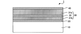
- FIG. 1 is a schematic configuration diagram of a pyroelectric infrared sensor element according to an embodiment of the present invention.
- the pyroelectric infrared sensor element 1 includes a support substrate 10, a lower electrode 20, an infrared absorbing and transmitting body 30 and an upper electrode 40 that are stacked in this order, and receives the upper electrode 40. Used as side.
- the shape and structure of the lower electrode 20 and the upper electrode 40 are not particularly limited, and may be, for example, a slit shape.
- the pyroelectric infrared sensor element 1 may further include another layer. For example, a heat transport layer made of an organic film may be provided above the upper electrode 40.
- the support substrate 10 is a sheet-like member having a thickness of about 5 to 200 ⁇ m made of a polymer material such as polyimide, polyamide, polyethylene terephthalate (PET), or polyethylene naphthalate (PEN). If the infrared absorbing / transmitting body 30 has a sufficient thickness and can be self-supporting, the support substrate 10 can be omitted.
- a polymer material such as polyimide, polyamide, polyethylene terephthalate (PET), or polyethylene naphthalate (PEN).
- the lower electrode 20 is made of a material having infrared reflectivity.
- the lower electrode 20 is formed by vapor deposition or sputtering using a metal such as aluminum (Al), gold (Au), silver (Ag), or an alloy thereof. can do.
- the thickness of the lower electrode 20 is not particularly limited, but can be about 100 nm.
- the infrared absorbing / transmitting body 30 includes two pyroelectric layers 31a and 31b arranged above and below, and a separation layer 32 is interposed between the pyroelectric layers 31a and 31b.
- the infrared absorbing / transmitting body 30 is a member that has both transparency and absorptivity to infrared rays by being formed of a material that absorbs a part of infrared rays and transmits the remaining part. Infrared reflected light and transmitted light interfere inside.
- the pyroelectric layers 31a and 31b are made of an organic pyroelectric material such as a vinylidene fluoride (VDF) polymer or a copolymer of vinylidene fluoride and ethylene trifluoride (P (VDF / TrFE)). It is formed by a spin coating method, a vacuum deposition method, or the like, and is subjected to polarization processing by applying a triangular wave voltage or the like.
- VDF polymer include polyvinylidene fluoride (PVDF) and a VDF oligomer which is a low molecular weight product thereof.
- the separation layer 32 has a refractive index higher than that of the pyroelectric layer 31.
- the separation layer 32 has a refractive index of chromium, platinum, titanium oxide (TiO 2 ), nickel chromium (Ni—Cr) alloy, or the like. It can be formed by a vacuum deposition method or the like using an inorganic dielectric material such as a high metal, metal oxide, or alloy.
- the separation layer 32 has absorptivity and reflectivity for infrared rays, and is formed of, for example, an electrode material as described above.
- the upper electrode 40 is made of an infrared-absorbing material such as nickel (Ni), chromium (Cr), nickel chromium (Ni—Cr) alloy, and can be formed by a vacuum deposition method, a sputtering method, or the like. Although the thickness of the upper electrode 40 is not specifically limited, About 20 nm can be illustrated.
- the infrared absorbing and transmitting body 30 can also function as an optical multilayer filter that efficiently absorbs only infrared rays in a desired wavelength region.
- the wavelength of incident light desired to be absorbed by a specific pyroelectric layer is ⁇
- the thickness and refractive index of this pyroelectric layer are d
- n is set
- the thicknesses of the pyroelectric layers 31a and 31b are preferably different from each other so that high infrared absorptivity can be obtained over the entire desired wavelength range.
- the thickness of the separation layer 32 is preferably as thin as possible so as not to prevent the reflection of infrared rays at the interface, for example, about 20 nm.
- the detection wavelength range is preferably set as appropriate according to the purpose. For example, when used as a CO 2 gas sensor, the detection wavelength is set to 3 to 4 ⁇ m, and when used as a human sensor, the detection wavelength is set to 5 Set to ⁇ 15 ⁇ m.
- the lower electrode 20 has infrared reflectivity, while the upper electrode 40 has infrared absorbability, so that infrared light incident on the infrared absorbing / transmitting body 30 from the upper electrode 40 side is reflected at the interface with the lower electrode 20. . Furthermore, when the upper electrode 40 has both infrared absorptivity and reflectivity, infrared rays are reflected multiple times between the lower electrode 20 and the upper electrode 40.
- the combination of the Fabry-Perot interference generated thereby and the plurality of pyroelectric layers 31a and 31b can further increase the infrared absorptivity of the infrared absorbing and transmitting body 30 in the entire desired wavelength range, thereby achieving high sensitivity. be able to.
- the lower electrode 20 may have infrared absorptivity like the upper electrode 40.
- the infrared reflective layer below the lower electrode 20, the infrared light transmitted through the lower electrode 20 can be reflected at the interface with the infrared reflective layer.
- the pyroelectric layers 31a and 31b are not necessarily organic pyroelectric materials. If a refractive index difference from the separation layer 32 is obtained, inorganic materials such as lead zirconate titanate (PZT) and barium titanate are used. You may form with a pyroelectric material. When the refractive index difference between the pyroelectric layer and the separation layer is small, the number of layers of the pyroelectric layer and the separation layer is increased, and a multilayer structure (for example, the pyroelectric layer is 10 High sensitivity can be achieved by using an infrared absorbing / transmitting material of about 50 layers.
- PZT lead zirconate titanate
- barium titanate barium titanate
- both the uppermost layer and the lowermost layer of the infrared absorbing / transmitting body be the pyroelectric layer.
- the pyroelectric layers 31a and 31b of the present embodiment use those having a refractive index smaller than the refractive index of the separation layer 32. However, the pyroelectric layers 31a and 31b are smaller than the refractive index of the separation layer 32. It may have a high refractive index.
- the infrared absorbing and transmitting body 30 of the present embodiment has a configuration in which the pyroelectric effect is generated in the pyroelectric layers 31a and 31b, while the pyroelectric effect is not generated in the separation layer 32.
- the pyroelectric effect may be generated in both the pyroelectric layers 31a and 31b and the separation layer 32.
- the infrared absorption spectrum fitting analysis was performed using the pyroelectric infrared sensor element 1 having the configuration shown in FIG. 1 as an example. That is, the structure, film thickness, and optical constants (dielectric constant, attenuation coefficient, etc.) of the pyroelectric infrared sensor element 1 are initially set to construct an optical model, and measured with an infrared absorption spectrum calculated by simulation and a sample product. The film thickness and optical constants were determined from the convergence results obtained by fitting the infrared absorption spectrum.
- the pyroelectric infrared sensor element of the example was produced. Further, as a comparative example, a pyroelectric infrared sensor element in which the infrared absorbing and transmitting body is composed of only a single pyroelectric layer was produced.
- the material and thickness of each layer in the examples and comparative examples are as shown in Table 1 below.
- the thickness of each pyroelectric layer 31a, 31b included in the infrared absorbing / transmitting body is set to 400 nm and 900 nm, respectively.
- three types having different thicknesses of the infrared absorbing and transmitting materials were designated as Comparative Examples 1 to 3, respectively.
- the thicknesses of the infrared absorbing and transmitting bodies of Comparative Examples 1 and 2 correspond to the thicknesses of the pyroelectric layers 31a and 31b of the example, respectively, and the thickness of the infrared absorbing and transmitting body of Comparative Example 3 is the respective pyroelectrics of the example. This corresponds to the sum of the thicknesses of the body layers 31a and 31b.
- the increase / decrease characteristic of the absorptance due to Fabry-Perot interference at the layer interface is reduced by the multilayering of the pyroelectric layers 31a and 31b, and in the entire wavelength range of 1 to 15 ⁇ m.
- a high absorption rate was obtained (average absorption rate 72.6%).
- Comparative Examples 1 to 3 a significant drop in the absorption rate due to Fabry-Perot interference occurs at different frequencies, and the average absorption rates are 66.2%, 58.0%, and 58, respectively. It was a low value of 2% compared to the example.
- the spectroscope 103 is irradiated with infrared light frequency-modulated by a chopper 102 having a chopping frequency of 0.2 Hz from a ceramic heater 101 having a temperature of 1500 K, and the pyroelectric infrared sensor element 1 through the slit 104. It was made to enter.
- the output voltage V out of the pyroelectric infrared sensor element 1 was measured with an oscilloscope 105 and amplified with a lock-in amplifier 106. The result is shown in FIG.
- FIG. 5 shows the wavelength dispersion characteristics of infrared absorptivity and voltage sensitivity for Example and Comparative Example 2.
- the wavelength 2 of Comparative Example 2 Including the drop at 4 ⁇ m, the voltage sensitivity also tends to increase as the infrared absorption rate increases for the same amount of infrared input, confirming that the voltage sensitivity of the example is better than that of Comparative Example 2. did.
- the infrared absorptance and voltage sensitivity are greatly reduced at a wavelength of 2.4 ⁇ m (infrared absorptance 35%, voltage sensitivity 19.5 V / W), while the example has the same wavelength.
- the drop in infrared absorption rate and voltage sensitivity was improved (infrared absorption rate 84%, voltage sensitivity 121.6 V / W).
- FIG. 6 is a diagram showing a result of obtaining the influence of multilayering of the infrared absorbing and transmitting body on the infrared absorption rate by simulation by changing the number of pyroelectric layers stacked via the separation layer. The higher the number of pyroelectric layers, the more stable the infrared absorption rate in a wide wavelength range.
Landscapes
- Physics & Mathematics (AREA)
- General Physics & Mathematics (AREA)
- Spectroscopy & Molecular Physics (AREA)
- Photometry And Measurement Of Optical Pulse Characteristics (AREA)
Abstract
所望の波長域の赤外線を小型且つ高感度で検出することができる焦電型赤外線センサ素子を提供する。 上部電極40と下部電極20との間に赤外線吸収透過体30が配置され、赤外線吸収透過体30は、複数の焦電体層31a,31bの間に、焦電体層31a,31bの屈折率と異なる屈折率を有する分離層32が介在されている。焦電体層31a,31bは、例えば有機焦電体から形成することができ、分離層32は、例えば無機材料から形成することができる。
Description
本発明は、焦電型赤外線センサ素子に関する。
焦電型赤外線センサ素子は、一般に、上部電極と下部電極との間に焦電体からなる赤外線吸収透過体を配置して構成される。赤外線吸収透過体の材料として、例えば特許文献1にはフッ化ビニリデンオリゴマーが開示されている。
焦電型赤外線センサ素子を用いて赤外線検出装置を構成する場合、人体検知、ガス検知、炎検知などの用途に応じて検出波長が異なることから、使用目的に応じた波長フィルタリングを行うことができるように、焦電型赤外線センサ素子を収容するケーシングの窓部にバンドパスフィルタ等の光学フィルタを配置することが従来から行われている。
ところが、従来のように焦電型赤外線センサ素子と光学フィルタとを個別に作製・配置する場合には、製造工程が煩雑でコスト高になり易いだけでなく、赤外線検出装置の小型化が難しいという問題があった。
そこで、本発明は、所望の波長域の赤外線を小型且つ高感度で検出することができる焦電型赤外線センサ素子の提供を目的とする。
本発明の前記目的は、上部電極と下部電極との間に赤外線吸収透過体が配置され、前記赤外線吸収透過体は、複数の焦電体層を有し、前記焦電体層の間に前記焦電体層の屈折率と異なる屈折率を有する分離層が介在されている焦電型赤外線センサ素子により達成される。
この焦電型赤外線センサ素子において、前記焦電体層は有機焦電体からなることが好ましく、前記分離層は無機材料からなることが好ましい。より好ましくは、前記焦電体層は、フッ化ビニリデン(VDF)の重合体、または、フッ化ビニリデンと三フッ化エチレンとの共重合体(P(VDF/TrFE))の少なくともいずれかを含む。
また、この焦電型赤外線センサ素子において、前記赤外線吸収透過体は、最上層および最下層がいずれも前記焦電体層となるように、前記焦電体層および前記分離層が交互に繰り返し配置された多層構造とすることができる。
前記焦電体層の屈折率は、前記分離層の屈折率よりも低いことが好ましい。
また、前記上部電極は、赤外線吸収性を有する材料から形成されて受光側に配置されることが好ましく、前記下部電極は、赤外線反射性を有する材料からなることが好ましい。
本発明によれば、所望の波長域の赤外線を小型且つ高感度で検出することができる焦電型赤外線センサ素子を提供することができる。
以下、本発明の実施の形態について、添付図面を参照して説明する。図1は、本発明の一実施形態に係る焦電型赤外線センサ素子の概略構成図である。図1に示すように、焦電型赤外線センサ素子1は、支持基板10、下部電極20、赤外線吸収透過体30および上部電極40が、この順に積層されて構成されており、上部電極40を受光側として使用される。下部電極20および上部電極40の形状や構造は特に限定されるものではなく、例えば、スリット状等であってもよい。また、焦電型赤外線センサ素子1は、更に他の層を含むものであってもよく、例えば、上部電極40の上方に有機膜からなる熱輸送層を設けてもよい。
支持基板10は、例えばポリイミド、ポリアミド、ポリエチレンテレフタレート(PET)、ポリエチレンナフタレート(PEN)等の高分子材料からなる厚みが5~200μm程度のシート状部材である。なお、赤外線吸収透過体30が十分な厚みを有することで自立可能な場合には、支持基板10を備えない構成にすることもできる。
下部電極20は、赤外線反射性を有する材料からなり、例えば、アルミニウム(Al)、金(Au)、銀(Ag)などの金属やこれらの合金を使用して、蒸着法やスパッタ法等により形成することができる。下部電極20の厚みは特に限定されないが、100nm程度を例示することができる。
赤外線吸収透過体30は、上下に配置された2つの焦電体層31a,31bを備えており、これら焦電体層31a,31bの間に分離層32が介在されて構成されている。赤外線吸収透過体30は、赤外線の一部を吸収しつつ残部を透過させる材料により形成されることで、赤外線に対して透過性および吸収性の双方を有する部材であり、赤外線吸収透過体30の内部で赤外線の反射光と透過光とが干渉する。
焦電体層31a,31bは、フッ化ビニリデン(VDF)の重合体や、フッ化ビニリデンと三フッ化エチレンとの共重合体(P(VDF/TrFE))等の有機焦電体からなり、スピンコート法や真空蒸着法等により形成されて、三角波電圧の印加等により分極処理が施されている。VDFの重合体としては、ポリフッ化ビニリデン(PVDF)や、その低分子量体であるVDFオリゴマーを好ましく例示することができる。
分離層32は、焦電体層31の屈折率よりも高い屈折率を有しており、例えば、クロムや白金、酸化チタン(TiO2)、ニッケルクロム(Ni-Cr)合金等の屈折率が高い金属、金属酸化物、合金等の無機誘電体材料を用いて、真空蒸着法等により形成することができる。分離層32は、赤外線に対して吸収性および反射性を有しており、上記のように、例えば電極材から形成される。
上部電極40は、例えばニッケル(Ni)、クロム(Cr)、ニッケルクロム(Ni-Cr)合金等の赤外線吸収性を有する材料から形成され、真空蒸着法やスパッタ法等により形成することができる。上部電極40の厚みは特に限定されないが、20nm程度を例示することができる。
上記の構成を備える焦電型赤外線センサ素子1は、赤外線吸収透過体30が備える2つの焦電体層31a,31bにおいて、赤外線の吸収による温度変化により電気信号が生じると共に、これら焦電体層31a,31bが、屈折率の異なる分離層32によって分離されているため、赤外線吸収透過体30を、所望の波長域の赤外線のみを効率良く吸収する光学多層膜フィルタとしても機能させることができる。
すなわち、特定の焦電体層(焦電体層31aまたは焦電体層31bのいずれか)に吸収させたい入射光の波長をλとし、この焦電体層の膜厚および屈折率をdおよびnとすると、λ=4ndとなるように膜厚および屈折率を設定する。これにより、焦電体層と分離層との界面での反射により焦電体層の内部を互いに逆方向に進む光同士が弱め合うので、焦電体層の赤外線吸収率が最大になり、波長λの赤外線の検出感度を高めることができる。各焦電体層31a,31bの厚みは、所望の波長域全体で高い赤外線吸収性が得られるように、互いに相違することが好ましい。分離層32の膜厚は、界面での赤外線の反射を妨げない程度になるべく薄くすることが好ましく、例えば20nm程度である。
また、このように赤外線吸収透過体30が光学フィルタを兼ねることにより、検出波長に対応したバントパスフィルタを別に用意して設置する必要がないため、製造コストの低減や小型化を図ることができる。検出波長域は目的に応じて適宜設定することが好ましく、例えばCO2ガスセンサとして使用する場合には、検出波長を3~4μmに設定し、人感センサとして使用する場合には、検出波長を5~15μmに設定する。
また、下部電極20は赤外線反射性を有する一方、上部電極40は赤外線吸収性を有することにより、上部電極40側から赤外線吸収透過体30に入射した赤外線が、下部電極20との界面で反射する。更に、上部電極40が赤外線吸収性と共に反射性も有する場合には、下部電極20と上部電極40との間で赤外線が多重反射する。これにより発生するファブリペロー干渉と、複数の焦電体層31a,31bとの組み合わせによって、所望の波長域全体における赤外線吸収透過体30の赤外線吸収性をより高めることができ、高感度化を図ることができる。但し、下部電極20は、上部電極40と同様に赤外線吸収性を有するものであってもよい。この場合は、下部電極20の下方に赤外線反射層を設けることで、下部電極20を透過した赤外線を赤外線反射層との界面で反射させることができる。
焦電体層31a,31bを構成する有機焦電体は、上記以外に、炭素(C)と窒素(N)のCNを極性部位とするシアン化ビニリデン系化合物、尿素結合部分(NH-C=O-NH)を極性部位とするポリ尿素などのウレタン系化合物、水素結合が極性部位として働くポリアミド化合物であるナイロン(特に炭素数7と11のナイロン7、ナイロン11)、OH基を有するポリ乳酸L体などの一部のポリエステル材料が挙げられる。
また、焦電体層31a,31bは、必ずしも有機焦電体である必要はなく、分離層32との屈折率差が得られれば、チタン酸ジルコン酸鉛(PZT)やチタン酸バリウムなどの無機焦電体により形成してもよい。焦電体層および分離層の屈折率差が小さい場合には、焦電体層および分離層の積層数を増加させてそれぞれが交互に繰り返し配置された多層構造(例えば、焦電体層が10~50層程度)の赤外線吸収透過体にすることで、高感度化を図ることができる。この場合、赤外線吸収透過体の最上層および最下層がいずれも前記焦電体層となるように構成することが好ましい。本実施形態の焦電体層31a,31bは、屈折率が分離層32の屈折率よりも小さいものを使用しているが、焦電体層31a,31bは、分離層32の屈折率よりも高い屈折率を有するものであってもよい。
本実施形態の赤外線吸収透過体30は、焦電体層31a,31bで焦電効果が生じる一方、分離層32では焦電効果が生じない構成にしているが、分離層32を焦電体材料により形成して、焦電体層31a,31bおよび分離層32の双方で焦電効果が生じるように構成してもよい。
以下、実施例を挙げて本発明を更に詳細に説明する。但し、本発明は、これらの実施例に限定されるものではない。
図1に示す構成の焦電型赤外線センサ素子1を実施例として、赤外線吸収スペクトルのフィッティング解析を行った。すなわち、焦電型赤外線センサ素子1の構造、膜厚、光学定数(誘電率、減衰係数等)を初期設定して光学モデルの構築を行い、シミュレーションにより算出した赤外線吸収スペクトルとサンプル品で測定した赤外線吸収スペクトルとをフィッティングして得られた収束結果から、膜厚や光学定数を決定した。
上記のフィッティング解析に基づいて、実施例の焦電型赤外線センサ素子を作製した。また、比較例として、赤外線吸収透過体が焦電体層の単層のみからなる焦電型赤外線センサ素子を作製した。実施例および比較例の各層の材料および厚みは下記の表1の通りである。
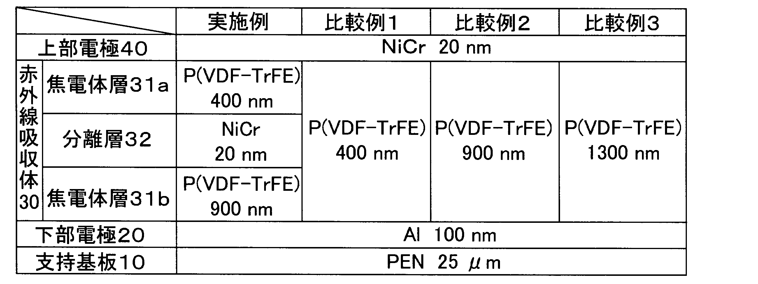
実施例は、赤外線吸収透過体が備える各焦電体層31a,31bの厚みを、それぞれ400nm、900nmとしたものである。一方、比較例は、赤外線吸収透過体の厚みが異なる3種類をそれぞれ比較例1~3とした。比較例1および2の赤外線吸収透過体の厚みは、実施例の各焦電体層31a,31bの厚みにそれぞれ相当し、比較例3の赤外線吸収透過体の厚みは、実施例の各焦電体層31a,31bの厚みを合計したものに相当する。実施例および比較例1~3の赤外線吸収スペクトルの測定結果を図2に示す。赤外線吸収率の測定には、フーリエ変換赤外分光光度計(FT-IR)を用いた。
図2に示すように、実施例は、層界面でのファブリペロー干渉に起因する吸収率の増減特性が、焦電体層31a,31bの多層化によって低減され、1~15μmの波長域全体において高い吸収率が得られた(平均吸収率72.6%)。これに対し、比較例1~3は、いずれもファブリペロー干渉による吸収率の顕著な落ち込みが、それぞれ異なる周波数で生じており、平均吸収率は、それぞれ66.2%、58.0%、58.2%と、実施例に比べて低い値であった。
次に、上記の実施例および比較例1~3について、図3に示す測定装置を用いて焦電応答を測定した。図3に示すように、温度が1500Kのセラミックヒータ101から、チョッピング周波数が0.2Hzのチョッパ102により周波数変調した赤外線を分光器103に照射し、スリット104を介して焦電型赤外線センサ素子1に入射させた。焦電型赤外線センサ素子1の出力電圧Voutは、オシロスコープ105により測定し、ロックインアンプ106により増幅させた。この結果を図4に示す。
図4に示すように、実施例は比較例1~3と比べて大きな出力電圧が得られており高感度であった。図5に、実施例および比較例2について、赤外線吸収率と電圧感度の波長分散特性を示す。一部測定環境内に存在するCO2やH2Oの吸収が原因で波長が4μmおよび7μm付近の測定誤差がみられるが、短波長側(7.5μm以下)では、比較例2の波長2.4μmにおける落ち込みを含めて、同じ赤外線入力量に対して赤外線吸収率が大きくなると電圧感度も高くなる傾向を示しており、比較例2に比べて実施例の電圧感度が良好であることを確認した。特に、比較例2は、波長2.4μmにおいて赤外線吸収率および電圧感度が大きく落ち込んでいるのに対し(赤外線吸収率35%、電圧感度19.5V/W)、実施例は、同じ波長での赤外線吸収率および電圧感度の落ち込みが改善された(赤外線吸収率84%、電圧感度121.6V/W)。
図6は、分離層を介して積層される焦電体層の積層数を変化させて、赤外線吸収透過体の多層化が赤外線吸収率に与える影響をシミュレーションにより求めた結果を示す図である。焦電体層の積層数が増加するほど、広い波長域において高い赤外線吸収率が安定する結果になった。
1 焦電型赤外線センサ素子
20 下部電極
30 赤外線吸収透過体
31a,31b 焦電体層
32 分離層
40 上部電極
20 下部電極
30 赤外線吸収透過体
31a,31b 焦電体層
32 分離層
40 上部電極
Claims (6)
- 上部電極と下部電極との間に赤外線吸収透過体が配置され、
前記赤外線吸収透過体は、複数の焦電体層を有し、
前記焦電体層の間に、前記焦電体層の屈折率と異なる屈折率を有する分離層が介在されている焦電型赤外線センサ素子。 - 前記焦電体層は有機焦電体からなり、前記分離層は無機材料からなる請求項1に記載の焦電型赤外線センサ素子。
- 前記焦電体層は、フッ化ビニリデン(VDF)の重合体、または、フッ化ビニリデンと三フッ化エチレンとの共重合体(P(VDF/TrFE))の少なくともいずれかを含む請求項2に記載の焦電型赤外線センサ素子。
- 前記赤外線吸収透過体は、最上層および最下層がいずれも前記焦電体層となるように、前記焦電体層および前記分離層が交互に繰り返し配置された多層構造である請求項1に記載の焦電型赤外線センサ素子。
- 前記焦電体層の屈折率は、前記分離層の屈折率よりも低い請求項1に記載の焦電型赤外線センサ素子。
- 前記上部電極は、赤外線吸収性を有する材料から形成されて受光側に配置されており、
前記下部電極は、赤外線反射性を有する材料からなる請求項1に記載の焦電型赤外線センサ素子。
Applications Claiming Priority (2)
| Application Number | Priority Date | Filing Date | Title |
|---|---|---|---|
| JP2016-092996 | 2016-05-06 | ||
| JP2016092996A JP2017201262A (ja) | 2016-05-06 | 2016-05-06 | 焦電型赤外線センサ素子 |
Publications (1)
| Publication Number | Publication Date |
|---|---|
| WO2017191746A1 true WO2017191746A1 (ja) | 2017-11-09 |
Family
ID=60203104
Family Applications (1)
| Application Number | Title | Priority Date | Filing Date |
|---|---|---|---|
| PCT/JP2017/015422 Ceased WO2017191746A1 (ja) | 2016-05-06 | 2017-04-17 | 焦電型赤外線センサ素子 |
Country Status (2)
| Country | Link |
|---|---|
| JP (1) | JP2017201262A (ja) |
| WO (1) | WO2017191746A1 (ja) |
Citations (7)
| Publication number | Priority date | Publication date | Assignee | Title |
|---|---|---|---|---|
| JPS612025A (ja) * | 1984-06-14 | 1986-01-08 | Murata Mfg Co Ltd | 一次元焦電型センサアレイ |
| JPS63134921A (ja) * | 1986-11-12 | 1988-06-07 | エヌ・ベー・フィリップス・フルーイランペンファブリケン | 赤外線検出装置 |
| JPH06307938A (ja) * | 1993-04-22 | 1994-11-04 | Mitsubishi Cable Ind Ltd | 焦電型赤外線温度センサ |
| JPH11132856A (ja) * | 1997-10-24 | 1999-05-21 | Masanori Okuyama | 熱型赤外線検出素子、熱型赤外線検出素子の製造方法、赤外線撮像システムおよび赤外線撮像装置 |
| WO2011071011A1 (ja) * | 2009-12-09 | 2011-06-16 | パナソニック電工株式会社 | 赤外線式炎検知器 |
| JP2013108970A (ja) * | 2011-10-25 | 2013-06-06 | Panasonic Corp | 赤外線検出装置 |
| US20150035110A1 (en) * | 2013-08-01 | 2015-02-05 | The Regents Of The University Of California | Pyroelectric aluminum nitride mems infrared sensor with selective wavelength infrared absorber |
Family Cites Families (1)
| Publication number | Priority date | Publication date | Assignee | Title |
|---|---|---|---|---|
| JP5708020B2 (ja) * | 2011-02-24 | 2015-04-30 | セイコーエプソン株式会社 | 熱型光検出器、熱型光検出装置、電子機器および熱型光検出器の製造方法 |
-
2016
- 2016-05-06 JP JP2016092996A patent/JP2017201262A/ja active Pending
-
2017
- 2017-04-17 WO PCT/JP2017/015422 patent/WO2017191746A1/ja not_active Ceased
Patent Citations (7)
| Publication number | Priority date | Publication date | Assignee | Title |
|---|---|---|---|---|
| JPS612025A (ja) * | 1984-06-14 | 1986-01-08 | Murata Mfg Co Ltd | 一次元焦電型センサアレイ |
| JPS63134921A (ja) * | 1986-11-12 | 1988-06-07 | エヌ・ベー・フィリップス・フルーイランペンファブリケン | 赤外線検出装置 |
| JPH06307938A (ja) * | 1993-04-22 | 1994-11-04 | Mitsubishi Cable Ind Ltd | 焦電型赤外線温度センサ |
| JPH11132856A (ja) * | 1997-10-24 | 1999-05-21 | Masanori Okuyama | 熱型赤外線検出素子、熱型赤外線検出素子の製造方法、赤外線撮像システムおよび赤外線撮像装置 |
| WO2011071011A1 (ja) * | 2009-12-09 | 2011-06-16 | パナソニック電工株式会社 | 赤外線式炎検知器 |
| JP2013108970A (ja) * | 2011-10-25 | 2013-06-06 | Panasonic Corp | 赤外線検出装置 |
| US20150035110A1 (en) * | 2013-08-01 | 2015-02-05 | The Regents Of The University Of California | Pyroelectric aluminum nitride mems infrared sensor with selective wavelength infrared absorber |
Also Published As
| Publication number | Publication date |
|---|---|
| JP2017201262A (ja) | 2017-11-09 |
Similar Documents
| Publication | Publication Date | Title |
|---|---|---|
| CN109642989B (zh) | 光学模块和使用该光学模块的光学装置 | |
| EP2770311A2 (en) | Terahertz wave detection device, camera, imaging device, and measuring device | |
| US9335217B2 (en) | Pyroelectric aluminum nitride MEMS infrared sensor with selective wavelength infrared absorber | |
| CN109642822B (zh) | 光谱仪和利用其的光谱测量方法 | |
| US20160139038A1 (en) | Gas sensor | |
| Mitmit et al. | Infrared wavelength-specific gas sensing with pyroelectricity at room temperature | |
| US11460399B2 (en) | Spectrally selective pyroelectric detection device and associated method of use | |
| US9274005B2 (en) | Device and method for increasing infrared absorption in MEMS bolometers | |
| KR20140143326A (ko) | 테라헤르츠파 검출 장치, 카메라, 이미징 장치 및 계측 장치 | |
| KR102715035B1 (ko) | 서브 파장 리플렉터를 포함하는 광학 필터, 분광기 및 이를 포함하는 전자 장치 | |
| CN111164394B (zh) | 光学感测装置和用于制造光学感测装置的方法 | |
| JP2017201262A (ja) | 焦電型赤外線センサ素子 | |
| US20160170108A1 (en) | Optical filter | |
| US10107743B2 (en) | Thermal infrared sensor and gas measuring apparatus | |
| WO2022238569A1 (en) | Metal organic framework photonic and electronic device for gas sensing | |
| Abdullah et al. | Device architecture for metasurface integrated uncooled SixGeyO1-xy infrared microbolometers | |
| US20060104319A1 (en) | Device for reflecting and detecting electromagnetic radiation | |
| Pinheiro et al. | A tunable fabry-perot optical filter for application in biochemical analysis of human's fluids | |
| Ashraf et al. | Fabrication of a mid-IR sensitive thermopile detector | |
| JP2011064673A (ja) | 熱型検出素子および分光検出器 | |
| US12607556B2 (en) | Molecular detector for surface-enhanced infrared absorption spectroscopy | |
| KR20120112901A (ko) | 적외선 흡수체 및 이를 이용한 적외선 검출기 | |
| Oishi et al. | SiO2/SiN multilayer-stack infrared absorber integrated on Pb (Zr0. 4, Ti0. 6) O3 film pyroelectric sensors on γ-Al2O3/Si substrate | |
| US20250004185A1 (en) | Angle selective filter | |
| KR101449655B1 (ko) | 파장 선택적 광 감지 센서 및 이를 이용한 센싱 방법 |
Legal Events
| Date | Code | Title | Description |
|---|---|---|---|
| NENP | Non-entry into the national phase |
Ref country code: DE |
|
| 121 | Ep: the epo has been informed by wipo that ep was designated in this application |
Ref document number: 17792679 Country of ref document: EP Kind code of ref document: A1 |
|
| 122 | Ep: pct application non-entry in european phase |
Ref document number: 17792679 Country of ref document: EP Kind code of ref document: A1 |