WO2017187304A2 - Digital frequency modulated continuous wave radar using handcrafted constant envelope modulation - Google Patents
Digital frequency modulated continuous wave radar using handcrafted constant envelope modulation Download PDFInfo
- Publication number
- WO2017187304A2 WO2017187304A2 PCT/IB2017/052279 IB2017052279W WO2017187304A2 WO 2017187304 A2 WO2017187304 A2 WO 2017187304A2 IB 2017052279 W IB2017052279 W IB 2017052279W WO 2017187304 A2 WO2017187304 A2 WO 2017187304A2
- Authority
- WO
- WIPO (PCT)
- Prior art keywords
- frequency
- radar system
- transmitter
- radio signal
- signal
- Prior art date
Links
Classifications
-
- G—PHYSICS
- G01—MEASURING; TESTING
- G01S—RADIO DIRECTION-FINDING; RADIO NAVIGATION; DETERMINING DISTANCE OR VELOCITY BY USE OF RADIO WAVES; LOCATING OR PRESENCE-DETECTING BY USE OF THE REFLECTION OR RERADIATION OF RADIO WAVES; ANALOGOUS ARRANGEMENTS USING OTHER WAVES
- G01S7/00—Details of systems according to groups G01S13/00, G01S15/00, G01S17/00
- G01S7/02—Details of systems according to groups G01S13/00, G01S15/00, G01S17/00 of systems according to group G01S13/00
- G01S7/35—Details of non-pulse systems
- G01S7/352—Receivers
-
- G—PHYSICS
- G01—MEASURING; TESTING
- G01S—RADIO DIRECTION-FINDING; RADIO NAVIGATION; DETERMINING DISTANCE OR VELOCITY BY USE OF RADIO WAVES; LOCATING OR PRESENCE-DETECTING BY USE OF THE REFLECTION OR RERADIATION OF RADIO WAVES; ANALOGOUS ARRANGEMENTS USING OTHER WAVES
- G01S13/00—Systems using the reflection or reradiation of radio waves, e.g. radar systems; Analogous systems using reflection or reradiation of waves whose nature or wavelength is irrelevant or unspecified
- G01S13/02—Systems using reflection of radio waves, e.g. primary radar systems; Analogous systems
- G01S13/06—Systems determining position data of a target
- G01S13/08—Systems for measuring distance only
- G01S13/32—Systems for measuring distance only using transmission of continuous waves, whether amplitude-, frequency-, or phase-modulated, or unmodulated
- G01S13/325—Systems for measuring distance only using transmission of continuous waves, whether amplitude-, frequency-, or phase-modulated, or unmodulated using transmission of coded signals, e.g. P.S.K. signals
-
- G—PHYSICS
- G01—MEASURING; TESTING
- G01S—RADIO DIRECTION-FINDING; RADIO NAVIGATION; DETERMINING DISTANCE OR VELOCITY BY USE OF RADIO WAVES; LOCATING OR PRESENCE-DETECTING BY USE OF THE REFLECTION OR RERADIATION OF RADIO WAVES; ANALOGOUS ARRANGEMENTS USING OTHER WAVES
- G01S13/00—Systems using the reflection or reradiation of radio waves, e.g. radar systems; Analogous systems using reflection or reradiation of waves whose nature or wavelength is irrelevant or unspecified
- G01S13/87—Combinations of radar systems, e.g. primary radar and secondary radar
-
- G—PHYSICS
- G01—MEASURING; TESTING
- G01S—RADIO DIRECTION-FINDING; RADIO NAVIGATION; DETERMINING DISTANCE OR VELOCITY BY USE OF RADIO WAVES; LOCATING OR PRESENCE-DETECTING BY USE OF THE REFLECTION OR RERADIATION OF RADIO WAVES; ANALOGOUS ARRANGEMENTS USING OTHER WAVES
- G01S13/00—Systems using the reflection or reradiation of radio waves, e.g. radar systems; Analogous systems using reflection or reradiation of waves whose nature or wavelength is irrelevant or unspecified
- G01S13/88—Radar or analogous systems specially adapted for specific applications
- G01S13/93—Radar or analogous systems specially adapted for specific applications for anti-collision purposes
- G01S13/931—Radar or analogous systems specially adapted for specific applications for anti-collision purposes of land vehicles
-
- G—PHYSICS
- G01—MEASURING; TESTING
- G01S—RADIO DIRECTION-FINDING; RADIO NAVIGATION; DETERMINING DISTANCE OR VELOCITY BY USE OF RADIO WAVES; LOCATING OR PRESENCE-DETECTING BY USE OF THE REFLECTION OR RERADIATION OF RADIO WAVES; ANALOGOUS ARRANGEMENTS USING OTHER WAVES
- G01S7/00—Details of systems according to groups G01S13/00, G01S15/00, G01S17/00
- G01S7/02—Details of systems according to groups G01S13/00, G01S15/00, G01S17/00 of systems according to group G01S13/00
- G01S7/28—Details of pulse systems
- G01S7/282—Transmitters
-
- G—PHYSICS
- G01—MEASURING; TESTING
- G01S—RADIO DIRECTION-FINDING; RADIO NAVIGATION; DETERMINING DISTANCE OR VELOCITY BY USE OF RADIO WAVES; LOCATING OR PRESENCE-DETECTING BY USE OF THE REFLECTION OR RERADIATION OF RADIO WAVES; ANALOGOUS ARRANGEMENTS USING OTHER WAVES
- G01S7/00—Details of systems according to groups G01S13/00, G01S15/00, G01S17/00
- G01S7/02—Details of systems according to groups G01S13/00, G01S15/00, G01S17/00 of systems according to group G01S13/00
- G01S7/35—Details of non-pulse systems
- G01S7/352—Receivers
- G01S7/358—Receivers using I/Q processing
-
- G—PHYSICS
- G01—MEASURING; TESTING
- G01S—RADIO DIRECTION-FINDING; RADIO NAVIGATION; DETERMINING DISTANCE OR VELOCITY BY USE OF RADIO WAVES; LOCATING OR PRESENCE-DETECTING BY USE OF THE REFLECTION OR RERADIATION OF RADIO WAVES; ANALOGOUS ARRANGEMENTS USING OTHER WAVES
- G01S13/00—Systems using the reflection or reradiation of radio waves, e.g. radar systems; Analogous systems using reflection or reradiation of waves whose nature or wavelength is irrelevant or unspecified
- G01S13/88—Radar or analogous systems specially adapted for specific applications
- G01S13/93—Radar or analogous systems specially adapted for specific applications for anti-collision purposes
- G01S13/931—Radar or analogous systems specially adapted for specific applications for anti-collision purposes of land vehicles
- G01S2013/9316—Radar or analogous systems specially adapted for specific applications for anti-collision purposes of land vehicles combined with communication equipment with other vehicles or with base stations
-
- G—PHYSICS
- G01—MEASURING; TESTING
- G01S—RADIO DIRECTION-FINDING; RADIO NAVIGATION; DETERMINING DISTANCE OR VELOCITY BY USE OF RADIO WAVES; LOCATING OR PRESENCE-DETECTING BY USE OF THE REFLECTION OR RERADIATION OF RADIO WAVES; ANALOGOUS ARRANGEMENTS USING OTHER WAVES
- G01S13/00—Systems using the reflection or reradiation of radio waves, e.g. radar systems; Analogous systems using reflection or reradiation of waves whose nature or wavelength is irrelevant or unspecified
- G01S13/88—Radar or analogous systems specially adapted for specific applications
- G01S13/93—Radar or analogous systems specially adapted for specific applications for anti-collision purposes
- G01S13/931—Radar or analogous systems specially adapted for specific applications for anti-collision purposes of land vehicles
- G01S2013/9327—Sensor installation details
- G01S2013/93271—Sensor installation details in the front of the vehicles
-
- G—PHYSICS
- G01—MEASURING; TESTING
- G01S—RADIO DIRECTION-FINDING; RADIO NAVIGATION; DETERMINING DISTANCE OR VELOCITY BY USE OF RADIO WAVES; LOCATING OR PRESENCE-DETECTING BY USE OF THE REFLECTION OR RERADIATION OF RADIO WAVES; ANALOGOUS ARRANGEMENTS USING OTHER WAVES
- G01S13/00—Systems using the reflection or reradiation of radio waves, e.g. radar systems; Analogous systems using reflection or reradiation of waves whose nature or wavelength is irrelevant or unspecified
- G01S13/88—Radar or analogous systems specially adapted for specific applications
- G01S13/93—Radar or analogous systems specially adapted for specific applications for anti-collision purposes
- G01S13/931—Radar or analogous systems specially adapted for specific applications for anti-collision purposes of land vehicles
- G01S2013/9327—Sensor installation details
- G01S2013/93272—Sensor installation details in the back of the vehicles
Definitions
- the present invention is directed to radar systems, and more particularly to radar systems for vehicles.
- a radar system typically transmits a signal and listens for the reflection of the signal from objects in the environment. By comparing the transmitted signal with the received signal, a radar system can determine the distance to an object. Using multiple transmissions, the velocity of the object can be determined. Moreover, using multiple transmitters and receivers, the location (angle) of the object can also be determined.
- FMCW frequency-modulated continuous waveform
- the transmitter of the radar system sends a continuous signal in which the frequency of the signal varies. This is sometimes called a chirp radar system.
- Mixing (multiplying) a waveform reflected from an object (also known as a target) with a replica of the transmitted signal results in a CW signal with a frequency that represents the distance between the radar transmitter/receiver and the target. By sweeping up in frequency and then down in frequency, the Doppler frequency can also be determined.
- An FMCW radar system comprises one or more constant envelope transmitters for transmitting radio signals that are frequency modulated.
- the frequency modulation uses codes to deviate the frequency from a mean or center frequency according to one of a limited number of shaped frequency transitions associated with a limited number of successive codes.
- the codes of each transmitter are different and preferably exhibit low cross-correlation.
- the frequency modulated signal may be produced by expressing the frequency modulation as a sequence of generated I and Q baseband vectors that are dependent on the limited number of successive codes and which have a constant envelope property where I 2 + Q 2 is a constant, for example, unity.
- the values are modulated on to a microwave carrier frequency for transmission by the radar transmitting antenna, for example by using an l,Q modulator.
- the I and Q waveforms are precomputed to depend on a limited number (N) of successive bits of a code, for example, 2 or 3 bits, and the precomputed waveforms are stored in a memory as numerical values.
- a plurality of l,Q values are stored in memory for each possible pattern of the N successive bits and a state variable indicative of the phase quadrant.
- the plurality of values are read from the memory sequentially for each new value of a code bit, the memory being addressed by the new bit, N-1 previous bits and the state variable.
- Each plurality of the l,Q values is engineered to obtain an optimum compromise between a number of often conflicting criteria, including compliance with a spectral mask, range resolution, the ease or difficulty of discriminating weak targets from close by strong targets, and correlation loss with target echo delays of a non-integral number of bit periods.
- the memory is organized as a plurality of N memories that are read at the code rate divided by N.
- Each pair of read l,Q values is digital to analog converted using a D to A converter that shapes the quantizing noise to reduce its spectral density near the microwave carrier frequency, and low-pass filtered to obtain analog l,Q signals that are applied to the l,Q modulator.
- a radar system for a vehicle includes a
- the transmitter transmits an amplified and frequency modulated radio signal.
- Each transmitter comprises a frequency generator, a code generator, a modulator, a constant-envelop power amplifier, and an antenna.
- the frequency generator is operable to or configured to generate the radio signal with a desired mean or center frequency.
- the code generator is operable to or configured to generate a sequence of chips at a selected chiprate. A modulation interval between successive chips is a reciprocal of the chiprate.
- the modulator frequency is operable to or configured to modulate the radio signal such that the frequency modulation comprises shaped frequency pulses.
- the shaped frequency pulses correspond to a first signal, the frequency of which deviates from the desired mean or center frequency during each of the modulation intervals according to a selected pulse shape.
- the constant-envelope power amplifier amplifies the frequency modulated radio signal at a desired transmit power level.
- the antenna transmits the radio signal.
- FIG. 1 is a plan view of an automobile equipped with one or more radar systems in accordance with the present invention
- FIG. 2A and FIG. 2B are block diagrams of radar systems in accordance with the present invention.
- FIG. 3 is a block diagram illustrating a flow of data structures through a radar system in accordance with the present invention
- FIG. 4 is a block diagram illustrating a radar system with a plurality of receivers and a plurality of transmitters (MIMO radar) for producing the data structures of FIG. 3, in accordance with the present invention
- FIG. 5 illustrates an exemplary transmitter architecture in accordance with the
- FIG. 6 illustrates an exemplary eye diagram for Gaussian minimum shift keying
- FIG. 7 is a graph illustrating the correlation of a transmitted signal with a transmitted code in accordance with the present invention.
- FIG. 1 1 is a graph illustrating variation of sidelobe levels with receiver filter BT in accordance with the present invention
- FIG. 12 is a graph illustrating variation of noise bandwidth and SNR with receiver filter BT in accordance with the present invention.
- FIG. 13 is a graph illustrating an eye diagram of modulation engineered to depend on 3 chips in accordance with the present invention.
- FIG. 14 is a graph illustrating the correlation function of the modulation of FIG. 13 in accordance with the present invention.
- FIG. 15 is a graph illustrating a comparison of the spectrum of regular GMSK with that of FIG. 14 in accordance with the present invention.
- FIG. 16 is a graph illustrating the correlation function of a more handcrafted
- FIG. 17 is a graph illustrating an eye diagram of the handcrafted waveform in
- FIG. 18 is a graph illustrating the spectrum of the handcrafted waveform in accordance with the present invention.
- FIG. 19 is a set of graphs illustrating trellis and constellation diagrams in
- FIG. 20 is a graph illustrating the eye diagram of MSK computed using 16 samples per chip in accordance with the present invention.
- FIG. 21 is a graph illustrating the spectrum of unfiltered MSK in accordance with the present invention.
- FIG. 22 is a graph illustrating the correlation function of MSK versus the number samples per chip in accordance with the present invention.
- FIG. 23 is a graph illustrating raised cosine digital FM in accordance with the
- FIG. 24 is a graph illustrating the eye diagram for raised cosine digital FM in
- FIG. 25 is a graph illustrating the spectrum of raised cosine digital FM in
- FIG. 26 is a graph illustrating the correlation function for raised cosine digital FM in accordance with the present invention.
- FIG. 27 is a graph illustrating the eradication of correlation sidelobe skirts of MSK with 8 samples/chip by waveform handcrafting in accordance with the present invention
- FIG. 28 is a graph illustrating the correlation function of handcrafted MSK at 4
- FIG. 29 is a graph illustrating the correlation function for raised cosine digital FM at
- FIG. 30 is a graph illustrating the variation of parameters with receiver BT for raised cosine transmitter modulation in accordance with the present invention.
- FIG. 31 is a graph illustrating the parameters of figure 30 on a finer dB scale in accordance with the present invention.
- FIG. 32 is a graph illustrating a class of shaping functions to be investigated in
- FIG. 33 is a graph illustrating other polynomial-based frequency-pulse shaping functions in accordance with the present invention.
- FIG. 34 is a flow diagram of a processing for simulating modulation in accordance with the present invention.
- FIG. 35 is a graph illustrating one possible eye diagram optimized for four (4)
- FIG. 36 is a graph illustrating the spectrum of the waveform of FIG. 35 with
- Gaussian post D to A filter BT 0.8 in accordance with the present invention.
- FIG. 37 is a graph illustrating the correlation sidelobes for the signals of FIGS. 35 and 36.
- Automobile radar systems become of greater utility the greater the object resolution achieved in ultimately the three dimensions of range, azimuth and elevation, as well as in Doppler shift, which indicates relative velocity of a target object.
- An ultimate goal is object recognition and hazard detection using the radar data, possibly in fusion with video data, map databases, and GPS positioning.
- FDMA Frequency Division Multiple Access
- TDMA Time Division Multiple Access
- CDMA Code Division Multiple Access
- DSSS Direct Sequence Spread Spectrum
- FHSS Frequency Hopping Spread Spectrum
- FM Analog Frequency Modulation
- Digital frequency modulation such as GSM's Gaussian Minimum Shift Keying (GMSK)
- GMSK Gaussian Minimum Shift Keying
- OFDM Orthogonal Frequency Division Multiplexing
- the delayed reflections are the wanted information.
- the signal reflected from an object or target and processed by a radar receiver has originated in the radar's own transmitter, which may be in intimate proximity to the receiver.
- the receiver can use information on exactly what was transmitted, and when, to aid in analyzing the received signal, and to determine the delays of target echoes which indicate their range.
- pulse radar in which a very short pulse of very high power microwave energy is transmitted during which time the receiver is blanked to prevent overload or damage; then the receiver is unblanked and listens for echoes received with various delays. The length of time the receiver can listen before the next transmitter pulse equates to the maximum range.
- the antenna may rotate between pulses to test for reflecting objects at different azimuths or elevations or both.
- the transmitter is not co-located with the receiver and uses a totally different antenna.
- the receiver thereby does not need to be blanked during the transmit pulse.
- CW radar In pulse radar systems, the transmitter duty factor and therefore the mean power is small; therefore, to achieve enough sensitivity for long range performance a high peak pulse power must be used. To overcome that, another type of radar called continuous wave (CW) radar is used. A CW radar transmits and receives all the time. The
- the transmitted signal has features in its waveform that enable the receiver to determine the delay of a received signal by determining the time difference between the transmitted feature and the received feature.
- the feature used is the instantaneous frequency.
- the transmitter frequency is changed linearly and very rapidly from a starting value to an ending value to create what is known as a chirp.
- a delayed signal will be received at an earlier value of the chirp frequency.
- the beat frequency which is the transmit-receive frequency difference
- the delay of the reflected chirp can be calculated. Because such a frequency difference cannot be distinguished from Doppler, a forward and backward chirp may be used alternately, producing a sawtooth frequency modulation.
- any Doppler has opposite effect on interpreting the forward chirp compared to the backward chirp, thus allowing range and Doppler to be separated.
- FMCW radar systems one issue is the extreme accuracy and linearity needed for the chirp signal.
- the greatest issue in CW radar is receiving at the same time as transmitting.
- the transmitted signal is much stronger than any received echo and can overload the receiver's limited dynamic range.
- pulse-CW radar Another version of CW radar aims to reduce the difficulty of receiving weak echoes from distant objects in the presence of the strong own transmitter signal. This is similar to pulse radar except that the transmitter duty factor is much higher, for example 50%.
- a modulated transmit pulse is transmitted for a duration that fills up the time to the furthest object and then switches off.
- the receiver attempts to receive strong echoes from nearby objects while the transmitter is transmitting, but when receiving weak later echoes from distant objects, the transmitter has already switched off, facilitating their detection. Improving near-far performance in radar systems is described in detail in U.S. patent application, Ser. No. 15/292,755, filed Oct. 13, 2016 ("the 755 patent”), which is hereby incorporated by reference herein in its entirety.
- digital codes are sometimes referred to as comprising a bit sequence and sometimes as comprising a chip sequence.
- chips and “bits” are used interchangeably herein, and mean binary valued quantities.
- the binary values are 0 or 1 in Boolean notation or +1 and -1 in numerical notation. They may also be abbreviated to just + and - signs.
- symbols is also known, and may apply to binary values or multi-valued quantities selected from a finite alphabet. When a multivalued quantity can exhibit 2 N different values, it can also be equated with N binary values or bits.
- the invention is described primarily for use in a digital FMCW radar in which
- Hybrid radars can also be made in which transmission and reception are simultaneous for a first period and then the transmitter switches off to allow the receiver to receive weak, late echoes without strong interference from the local transmitter, as discussed in the 755 patent.
- the distance resolution is ultimately related to the width of the autocorrelation function of the transmitted signal.
- Advanced algorithms such as Multiple Signal Classification (MUSIC) allow resolution less than, but still related to the width of the autocorrelation function.
- MUSIC Multiple Signal Classification
- the power spectrum is the Fourier transform of the autocorrelation function and so has a spectral occupancy inversely proportional to the range resolution.
- the receiver does not necessarily receive the transmitted signal with a matched filter, so deviations in the relationship between range resolution and signal autocorrelation function may arise. In that case, the correlation curve exhibited when the receiver correlates a received signal with a
- the correlation function With small delays of plus or minus two or three chips, the shape of the correlation function mimics the impulse response of the entire channel that exists between the transmitter's code generator and the point at which the received signal is extracted into the correlator. For large relative shifts of many chips or bits, the correlation function will exhibit the autocorrelation function of the digital code chosen. It is well known that Maximum Length Sequences exhibit autocorrelation functions that only have one large peak, and all sidelobes are at a level relative to the peak of -1/N, where N is the length of the code. If they can be used, this autocorrelation property is a desirable one for radar systems. [0062] As noted above, FMCW radar typically used chirp signals to determine range and Doppler.
- a digital FMCW radar transmits an RF signal which is frequency modulated with a digital code sequence to produce a transmitted signal that has good autocorrelation properties that facilitate range resolution while exhibiting good spectral containment.
- One type of frequency modulation that appears to have interesting properties in this regard is minimum shift keying (MSK).
- MSK minimum shift keying
- the signal vector lies at one of two diametrically opposite points along a line at right angles to the prior signal vector position.
- MSK is related to Offset QPSK in that the signal vector for even bits ends up at +/-1 while the signal vector for odd bits ends up at +/-j. The difference however is, that when the 1 ⁇ ->0 transitions of the digital code are filtered or shaped to contain the spectrum, the MSK signal remains at a constant amplitude while an OQPSK signal acquires amplitude modulation, requiring a linear transmit power amplifier to preserve it.
- Such linear power amplifiers have lower efficiency than constant envelope amplifiers because they do not operate at the optimum power point 100% of the time.
- a solid state constant envelope transmitter may achieve 60% efficiency while a linear power amplifier may achieve only 30% efficiency.
- the bandwidth of the transmitted RF signal using digital FM is proportional to the chiprate of the digital modulating code, while the rate at which the spectrum falls off outside of the main spectral lobe depends on the shaping applied to the frequency modulation. It is well known that filtering an MSK modulating waveform using a Gaussian filter produces, for some coincidental reason, the greatest ultimate rate of spectral fall-off outside the main occupied bandwidth. This was particularly exploited for the GSM digital cellular phone system which employed this modulation, termed Gaussian minimum shift keying (GMSK). In this application, versions of such modulations are described that are particularly optimized to meet criteria important in the radar application, rather than criteria important in the communications application, and other advantageous frequency modulation pulse shapes are disclosed.
- GMSK Gaussian minimum shift keying
- Radars with a single transmitter and a single receiver can determine distance to a target but cannot accurately determine a direction or an angle of a target from the radar sensor or system unless the antenna pattern is steered between pulses either
- each receiver receives and separates each echoed transmitter signal, thus resulting in N x M received results, where N is the number of transmitters and M is the number of receivers.
- N x M results can be post-combined in any number of ways according to a plurality of beamforming vectors, thereby achieving elevation and azimuth location of each signal as well as range and Doppler information.
- each transmission antenna is connected to a separate transmitter, and each receiver antenna is connected to a separate receiver.
- a radar system is known as a multiple-input, multiple-output (MIMO) radar system.
- FIG. 4 An exemplary MIMO radar system is illustrated in FIG. 4. With MIMO radar
- each transmitter signal is rendered distinguishable from every other transmitter by using appropriate differences in the modulation, for example, different digital code sequences.
- Each receiver correlates with each transmitter signal, producing a number of correlated outputs equal to the product of the number of receivers with the number of transmitters. The outputs are deemed to have been produced by a number of virtual receivers, which can exceed the number of physical receivers.
- a receiver may be referred to as a virtual receiver even when there is only a single transmitter, in order to avoid changing the terminology.
- the output of a given receiver receiving a transmitted signal from a given transmitter has a phase that depends on the loop distance from the transmitting antenna to the receiving antenna. Each transmit-receive combination produces a different loop phase due to the separation of their antennas.
- An exemplary radar system therefore determines the range of a target or the distance to a target principally by determining how long it takes an echo of transmitted RF signals to be heard back at the receivers. From this measured time-delay and knowing that the electromagnetic RF signals travel at the speed of light (or ultrasonic signals traveling at the speed of sound), the distance can be determined.
- the method of determining the time delay is by correlating a received RF signal with multiple time-shifts of the digital modulating code to produce correlations which are stored in range bins. The length of time over which coherent correlations can be performed is limited by the phase rotation caused by Doppler shift.
- partial correlations are combined while compensating for the Doppler-induced phase drift.
- the partial correlations may be stored for each virtual receiver and range in a 3-dimensional array called a radar data cube, as illustrated in FIG. 3, in which the three dimensions are virtual receiver number, range, and time or index of the partial correlation. Partial correlations for the same receiver and range are then submitted to an FFT, which combines them in a
- the radar data cube time dimension has been converted into a Doppler shift dimension which is more meaningful for characterizing a reflecting target or object as stationary or moving.
- the results across different virtual receivers may be combined by using beamforming matrices as mentioned above in order to achieve angular resolution in azimuth, elevation or both.
- the maximum Doppler shift may be based on four times the maximum speed of any one vehicle. For a maximum vehicle speed of 250km/hr, which can be reached on the German Autobahn for example, the maximum Doppler shift can be that of a 10OOkm/hr object, which is 74 KHz at 80 GHz. If a radar system's own velocity, which is presumed to be known, is digitally removed by applying a systematic phase de-twisting to the received data, the maximum Doppler shift drops to 37 KHz.
- the radar sensing system of the present invention may utilize aspects of the radar systems described in U.S. patent applications, Ser. No. 15/416,219, filed Jan. 26, 2017, Ser. No. 15/292,755, filed Oct. 13, 2016, Ser. No. 15/204,003, filed Jul. 7, 2016, and/or Ser. No. 15/204,002, filed Jul. 7, 2016, and/or U.S. provisional applications, Ser. No.
- FIG. 1 illustrates an exemplary radar system 100 configured for use in a vehicle 150.
- a vehicle 150 may be an automobile, truck, or bus, etc.
- the radar system 100 may comprise one or more transmitters and one or more receivers 104a- 104d which can be used jointly to realize a plurality of virtual radars. Other configurations are also possible.
- FIG. 1 illustrates a radar system 100 comprising one or more
- receivers/transmitters 104a-104d are placed to acquire and provide data for object detection and adaptive cruise control.
- the radar system 100 may be part of an Advanced Driver Assistance System (ADAS) for the automobile 150.
- ADAS Advanced Driver Assistance System
- FIG. 2A illustrates an exemplary radar system 200 with an antenna 202 that is time- shared between a transmitter 206 and a receiver 208 via a duplexer 204.
- output from the receiver 208 is received by a control and processing module 210 that processes the output from the receiver 208 to produce display data for the display 212.
- the control and processing module 210 is also operable to produce a radar data output that is provided to other control units.
- the control and processing module 210 is also operable to control the transmitter 206.
- FIG. 2B illustrates an alternative exemplary radar system 250 with a pair of
- antennas 202a, 202b an antenna 202a for the transmitter 206 and another antenna 202b for the receiver 208.
- pulse radar systems may use shared or separate antennas
- continuous-wave radars discussed herein will use separate antennas (for transmitting and receiving) because of their continuous operation.
- local spillover from transmitter to receiver is a huge signal having a short delay.
- a critical issue in CW radar is the removal by subtraction of this large local spillover signal, for the success of which an accurately defined modulation, as is disclosed herein, is essential.
- FIG. 4 illustrates an exemplary digitally-modulated continuous-wave radar system 400.
- Radar system 400 comprises a plurality of receivers and their respective antennas 406 and a plurality of transmitters and their respective antennas 408.
- the radar system 400 also includes a flash memory 412, and optionally a random access memory 410.
- the random access memory 410 for example, an external DRAM, may be used to store radar data cube(s) instead of using the limited internal (on-chip) memory (e.g., SRAM), and may also be used to store selected range bins from a greater number of radar data cubes for post processing to improve Doppler resolution or range resolution by tracking objects using Kalman filtering.
- the radar system may also include a variety of interconnections to an automotive network, e.g., Ethernet, CAN-FD, and/or Flexray.
- range resolution is related to the width of the
- a practical autocorrelation function width cannot be too small, otherwise it will have to be computed from the received signal with a sufficiently high sampling density to avoid missing the peak, and the results have to be stored in memory for further analysis, e.g. Doppler analysis. Therefore, computational power and on chip memory limitations, or, in the case of off-chip memory, I/O bandwidth limitations, limit the narrowness of the autocorrelation function that can be contemplated.
- one possible sampling density is one sample per chip period, obtained by correlating the transmitted sequence with different whole-chip shifts of the received signal.
- the chiprate may as well be doubled to reduce the width of the autocorrelation function, if bandwidth is available.
- bandwidth in the 80 GHz range is not the limitation. Therefore, the practical solution is to determine how many correlations per second can be computed and stored, and to equate that with the chip rate, such that correlations are to be computed only for whole-shifts of the received signal. Therefore, the characteristics of the autocorrelation functions, computed at whole-chip shifts, need to be investigated for digital code frequency- modulated signals.
- Several known algorithms exist for computing many correlations between one or more codes and multiple shifts of a received signal for example, a technique using FFTs for performing circular convolution is known.
- FIG. 5 illustrates an exemplary transmitter block diagram.
- a digital code generator 1010 is fed with a chiprate clock to produce a pseudorandom code for modulating the transmitter.
- the pseudorandom code preferably has good autocorrelation sidelobe properties at least up to a shift corresponding to the round-trip delay to a target at maximum range.
- the pseudorandom codes used by different transmitters of a MIMO radar should also be preferably mutually orthogonal or have low cross-correlation.
- the codes are merely random and a long correlation length relied upon to reduce cross correlation and autocorrelation to the point where subtractive interference cancellation can take over and further suppress strong targets to reveal weaker targets.
- sequences of random binary values may be provided by a truly random number generator or a pseudorandom number generator.
- a truly random number generator or a pseudorandom number generator.
- Such number generators are explained in more detail in U.S. patent application, Ser. No. 15/204,003, filed Jul. 7, 2016, which is hereby incorporated by reference herein in its entirety.
- the digital chip code from generator 1010 is fed to l,Q waveform selection logic module 1020, the purpose of which is to select the l,Q waveform to be modulated for the current chip period in dependence on the current chip and the chip history, in order to produce a signal having a signal frequency varying according to a predetermined shaping function.
- the number of possible waveforms is limited to eight, and thus requires three address bits (aO, a1 , and a2) from selection logic 1020 to address waveform memory 1030.
- the waveform depends on fewer than three successive chips.
- Each waveform may be described by a number of complex l,Q sample values, such as 4, 8, or 16 samples per chip.
- Counter 1040 is driven by a sample rate clock which is correspondingly 4, 8, or 16 times the chip rate clock that is used to select each l,Q sample pair in turn from the memory.
- Counter 1040 may be a "divide by 4" using two flip-flops for the case of 4 samples per chip, a 3-stage divider for 8 samples per chip, or a 4-stage divider for 16 samples/chip.
- the divided, down-sample rate clock is the desired chip rate clock and may be used to clock the digital code generator 1010.
- Each stage of counter 1040 produces a digital output as a further address bit to memory 1030.
- three counter bits (tO, t1 , and t2) are provided to memory 1030 to select one of the 8 samples.
- the selected sample (0 to 7) of waveform (0 to 7) comprises a digital I and Q value with a word length in the range of 8 to 16 bits.
- the digital I and Q values are fed into respective I and Q digital to analog converters (DAC) (1050A, 1050B) where they are converted to analog voltages or currents.
- DAC digital to analog converters
- the filtered balanced l,Q signals then modulate quadrature carrier signals produced by quadrature local oscillator (QLO) 1070 (may also be referred to as a frequency generator) using a pair of balanced modulators (1080A, 1080B) (may also be referred as l,Q modulators).
- QLO quadrature local oscillator
- the quadrature local oscillator may also be referred to as a carrier frequency generator operable to generate a carrier signal that is frequency modulated by the pair of balanced modulators (1080A, 1080B).
- the I, Q waveform selection logic 1020, the waveform memory 1030, the digital-to-analog converters 1050A, 1050B, the low pass filters 1060A, 1060B, and the balanced modulators 1080A, 1080B may be collectively referred to as the modulator.
- Gilbert-cell mixers using 28 nm MOSFET transistors have proven capable of modulating an 80 GHz carrier signal with 2 GB digital code rates.
- Gilbert cell mixers driven by similar QLOs may be used in the radar receiver in order to produce zero-IF, homodyne receivers.
- all transmitters and receivers preferably have a known phase relationship in order to allow the receiver outputs to be coherently combined by
- the desired phase relationship is guaranteed by injection-locking each transmitter and receiver's QLO (frequency generator) to a common standard.
- the common standard may be a sub-harmonic of the desired millimeter wave frequency, such as 1 /5th or 16 GHz, at which frequency it is easier to fabricate an accurate digital frequency synthesizer or generator to give programmable center or mean frequencies.
- the modulated signal at the radar carrier frequency is amplified to a transmit power level in constant envelope power amplifier (PA) 1090 which also operates push-pull (i.e. balanced).
- PA constant envelope power amplifier
- the push-pull PA 1090 is cross neutralized to reduce Miller feedback, improve the high frequency gain and reduce the S12 parameter.
- On-chip Balun transformer 1095 may be used to convert the push-pull signal to single ended to bring the signal off-chip through a ball-bond surrounded by grounded ball-bonds.
- FIG. 6 is a graph illustrating the typical eye diagram of the I and Q parts of the transmitted carrier using Gaussian minimum shift keying (GMSK) when no limit is placed on the number of stored waveforms; that is, each transition can depend on as much past history as the impulse response length of the selected Gaussian filter exhibits.
- GMSK Gaussian minimum shift keying
- the Gaussian premodulation filter is not fed with square waves (with a polarity equal to the bit values), but by impulses of unit area (with polarities given by the bit values).
- a square wave bit stream already has an implied sin(x)/x frequency-response shaped filter that shapes the waveform from impulses to square waves, and it is desired to investigate the performance of filters that are not constrained to include this inherent sin(x)/x factor.
- FIG. 34 illustrates a flow chart that was used to compute the waveforms of FIG. 6 and subsequent graphs.
- An 8-bit linear feedback shift register was used to generate a maximum length sequence of 255 bits at step 1 , and the sequence extended to 256 bits by adding one more bit to obtain a power of 2 bits. If the added bit is a zero, the extended 256 bit sequence will have an equal number of 1 's and 0's.
- each bit is placed in the center of a group of NSPB samples with the other samples zero, to represent an impulse having the desired bit polarity.
- the bit values are multiplied by NSPB to give the impulse unit area.
- the number of samples per bit is also chosen to be a power of 2, that is 4,8,16,32,64,128 or 256, so that the total number of samples is a power of 2 equal to 1024,2048,4096,8192,16384,32768 or 65536.
- the purpose is to allow the use of a fast, base-2 FFT at step 3 to produce the spectrum of the unfiltered impulse waveform.
- the spectrum is weighted by the frequency response of the shaping filter, e.g. a Gaussian filter.
- the filtered frequency modulating waveform must be integrated to obtain the phase waveform. This is conveniently done in step 5 while the signal is still in the frequency domain by dividing each spectral line by j times its own frequency. When the whole sequence is 256 bits long, the line spacing is 1/256 of the bitrate, so the frequency of each spectral line is simply determined.
- an inverse FFT produces the time waveform from the filtered and integrated spectrum.
- a suitable scaling is applied so that the desired frequency deviation or modulation index is obtained.
- the l,Q waveform is computed by taking the cosine and sine of the phase modulation samples, which also has the effect of reducing the phases modulo-2TT.
- a phase slope may be applied across the l,Q waveform to force it to join up end to end. This is equivalent to a very small frequency shift which can be used later if necessary to ensure that any filtering is correctly centered.
- the purpose of ensuring end-to-end continuity is that the FFT at step 10 assumes a cyclic waveform, without which artifacts may appear on the spectral sidelobes so calculated.
- step 8 the eye diagram is plotted, and manually a phase adjustment is
- step 9 the correlation function and autocorrelation functions may be calculated and displayed, and then the spectrum calculated at step 10 is displayed at step 1 1 .
- the flow chart may be extended to add other filtering such as the low pass filters 1060A and 1060B of FIG. 5, and receive filtering, and the effect on eye diagram, correlation function, and spectrum may be calculated and displayed as at earlier steps.
- other filtering such as the low pass filters 1060A and 1060B of FIG. 5, and receive filtering, and the effect on eye diagram, correlation function, and spectrum may be calculated and displayed as at earlier steps.
- phase shift mentioned above will be found to reduce the number of trajectories to a minimum by converging trajectories that were otherwise apparently divergent due to the phase shift produced by the modulating program. Manually adjusting the phase shift while observing the eye diagram will be seen to bring the picture into focus.
- each modulating bit polarity determines whether the l,Q vector rotates clockwise or anticlockwise by 90 degrees over the bit period.
- the l,Q vector will have rotated by either 0 or 180 degrees. In between, the vector lies at either 90 or 270 degrees.
- the polarity of even bits determines whether the vector will end up at 0 or 180 degrees and the polarity of odd bits determines whether the vector will end up at 90 or 270 degrees.
- the effect is cumulative, as shown in the table below:
- bit number 1 is a 1 , sending the phase clockwise from an
- phase and frequency-modulating bit sequence is:
- modulating bits Bi are derived from the desired modulating chip code Ci, according to the precoding equation (3) below:
- the final row is derived by multiplying the penultimate row of 1+jQ values by -(j) n .
- the frequency pulse shaping produced by the Gaussian filter may have an effect beyond the current chip.
- the phase change produced over one chip period by GMSK frequency pulses may fail to reach 90 degrees over one chip period, but when integrated over all chip periods affected by a given chip, the cumulative phase change to the signal produced is exactly +90 degrees so that the four principal terminal positions of the signal vector remain fixed and do not slowly rotate. This characteristic is maintained in this invention for all frequency pulse shapes considered by constraining the area integral of a frequency pulse shape over its entire impulse response length to be a fixed value.
- the local replica for correlation is simply derived from the code generator 1010 by delaying it if necessary.
- the twisted samples may be correlated with the shifts of the code C produced by the code generator 1010. If the receiver samples the received signal at N samples per chip, then selecting samples (e.g., 0, N, 2N, 3N), progressively twisting the samples and correlating with shifts of the code C, produces points on the correlation function (e.g., 0, N, 2N, 3N). Then, selecting points 1 , N+1 , 2N+1 , 3N+1 etc., progressively twisting them and correlating with C, produces points 1 , N+1 , 2N+1 , 3N+1 etc. of the correlation function. Continuing in this way produces the correlation function for all relative time shifts in steps of 1 /N of the chip period.
- the above described correlation function is illustrated in FIG. 7.
- the magnitude is plotted in dBs, and the horizontal divisions are one chip periods.
- This function is the correlation of the transmitted signal with the corresponding digital code, or equivalently it is the correlation of the received signal with the transmitted code when the receiver does not add additional filtering. Such a wideband receiver is undesirable however, as a bandpass filter is required to limit noise.
- the correlation function of FIG. 7 illustrates that, for sampling in the center of the eye, the peak correlation is unity as it just reproduces the mean power of the signal which has been set to unity, and the correlation at +/-1 chip period is about -14dB.
- the correlation at +1-2 chip periods is -80dB, so the transmitted signal depends substantially only on 3 consecutive bits when sampled at the center of the eye. This is exactly in correspondence with what can be seen in in FIG. 6. If however, the signal is mis-sampled by half a chip period, the correlation magnitudes are shown in the table below:
- a matched filter which is known to achieve maximum signal-to-noise ratio.
- a matched filter corresponds to correlating the signal with the complex conjugate of itself. This produces the autocorrelation function (ACF).
- ACF autocorrelation function
- FIG. 8 shows that with optimum sampling, the ACF at +/-1 chip period is about -7dB and is +/-31 dB at +/- 2 chip periods.
- the signal now therefore depends somewhat on five consecutive chips due to the additional ISI introduced by matched filtering. With half a chip mis-sampling, the ACF has the values shown in the table below.
- the signal is showing a dependence on either 4 chips or 6 chips, depending on whether a correlation level of -53dB is significant in the application.
- correlation values on the order of -30dB are not of significance because they do not significantly affect information error rates.
- a strong target echo can easily be 30dB above a weak target echo two chips away. Therefore, achieving low autocorrelation sidelobes is of greater importance in radar applications. If autocorrelation sidelobes remain high several chips away, strong target subtraction may then be necessary to reveal weaker target echoes with neighboring ranges. The complexity of strong target subtraction may therefore be reduced or eliminated entirely if correlation sidelobes can be adequately suppressed.
- the noise bandwidth of the filter is only 0.63 bitrates, which is a reduction of 1 .95 dB, substantially compensating for any loss of signal power and correlation magnitude.
- the signal-to-noise ratio is therefore about the same as with a matched filter correlator.
- the sidelobes however are now reduced from -31 dB at +/- 2 chips, using the matched filter, to -37 dB relative to the peak of correlation.
- the signal-to-noise ratio effects and the correlation sidelobes can now be explored as a function of the receiver's BT factor.
- 1 1 illustrates how the sidelobe levels at +/-0.5 chip, +/-1 chip, +/-1 .5 chips, +/- 2 chips and +/- 2.5 chips depend on receiver filter BT. Also, the noise bandwidth and peak correlation loss are shown, and combined to show the SNR loss involved in choosing higher receiver BT factors to reduce correlation sidelobes.
- the correlation at +/-0.5 chip has the practical significance that it represents the loss of peak correlation that occurs due to a target echo arriving with a delay that is a non-integral number of chip periods.
- FIG. 12 shows the latter as well as noise bandwidth, peak correlation loss, and net SNR loss on a finer dB scale.
- a 4-chip spread is evident from the 1 6 trajectories visible in FIG. 6, but the 5th chip dependence is there, only too small to be visible by the naked eye on the eye diagram.
- the waveform may therefore be handcrafted to converge these trajectories to a total of 8.
- the first step in handcrafting the waveform is to compute, for a given group of three chips within +/-1 chip of a waveform point, the average of all waveform values over the four other combinations of the two chips at +1-2 chips away.
- the average waveform points are intended to be stored at a given number of samples per chip in waveform memory (1030) of FIG. 5 for all 8 combinations of the group of three chips, and selected from memory when those 3 chip values are presented as address a2,a1 ,a0 from waveform selection logic (1020).
- the waveforms exhibit many symmetries, such as l/Q symmetry, time-reversal symmetry, and +/- symmetry, but for very high chiprates such as 2 GB/s it can be more burdensome to try to exploit those symmetries to reduce the memory size than to merely accept the full memory size. At lower chiprates, exploiting the symmetries might result in a net reduction of silicon area.
- those specific points at location X of the anomaly may depend only on the overlapping symbols b3 and b4 and may not depend on either the oldest bit b2 of the previous symbol shift nor the newest bit b5 of the subsequent symbol shift, but must be converged to a total of four points depending only on b3 and b4.
- step 1 two values at the left-hand side of the anomaly are designated as a1 and b1 and those on the right are designated as a2 and b2.
- step 2 if the value of ai.5 is the greater and the value of bi s is the smaller, the factor 1 +a is computed, by which waveform a must be reduced and waveform b increased at that notional point to force convergence, as:
- FIG. 16 illustrates an exemplary correlation function of the waveform when
- FIG. 17 confirms that the discontinuity has been removed by handcrafting
- FIG. 18 shows that the far-out spectrum has been reduced about 10 dB.
- the far-out spectrum may be further reduced by the low-pass roofing filters (1060A,B) with the reintroduction of some sidelobes of the correlation function.
- the filter cutoff frequencies should be, for example, Gaussian filters with a BT in the 1 .5 to 3 range. A sharp filter will produce more ringing and simulation has shown that a sharp cutoff of about 3 times the bitrate keeps the ringing on the ACF down to about the -70 dB level.
- GMSK waveforms have a 3-symbol dependence because of the 8 trajectory
- GSMK has that characteristic because an l-bit lying between two Q bits of equal polarity cannot achieve full amplitude as there is no Q zero crossing between the two equal Q-bits.
- FIG. 19 introduces some new diagrams that assist in understanding constant- envelope, digital modulation.
- Q1 is also encoded into a +dF frequency shift, the frequency remains at dF for a further time T and the phase changes by a further 90 degrees to the value +90 degrees at point Q1 .
- the constellation diagram shows by asterisks where the phase ends up at points I0,Q1 ,12,Q3, etc.
- Points denoted by In have terminal phases that are either 0 or 180, where the real part of the complex vector is +/-1 corresponding to the maximum eye-opening of the real part I, while the imaginary part goes to zero corresponding to a zero crossing of the imaginary part, Q.
- constellation points denoted by Qn have terminal phases that are either +90 or -90, and the l-values go to zero at those points.
- the frequency deviation is either +dF or -dF and changes abruptly from one value to the other, while the phase changes at a constant rate from one constellation point to the next.
- This modulation is known as "minimum shift keying" (MSK), and has the eye diagram illustrated in FIG. 20 and has the spectrum of FIG. 21 .
- the spectral sidelobes are seen to be of the order of 15-20 dB higher than those of the handcrafted GMSK modulation illustrated in FIG. 18, due to the absence of filtering to round the waveform transitions.
- the eye diagram illustrates a small anomaly at zero crossings which is partly an artifact of the graph-plotting program interpolating between the finite number of samples (16 in FIG. 20) used per bit period.
- the correlation function is therefore plotted in FIG. 22 with the number of samples per chip varying from 8 to 256, in factors of 2. It can be seen that the limit, for a large number of samples per bit, corresponding more closely to a continuous waveform, is a correlation function that falls precipitously to zero at +/-1 chip offset. With precise mid-eye sampling, the waveform therefore depends on only one chip, but with mis-sampling it depends on two adjacent chips, one l-chip and one Q-chip, as may be seen in the eye diagram of FIG. 20.
- FIG. 23 illustrates that a raised cosine frequency pulse that peaks at 2dF has this property.
- FIG. 24 illustrates the eye diagram for this modulation and
- FIG. 25 illustrates the spectrum, demonstrating the more rapid fall of the spectral sidelobes as a result of the raised cosine shaping.
- the correlation function before handcrafting the waveform is illustrated for 16 samples per chip in FIG. 26. After handcrafting the waveform by averaging all corresponding points to form a waveform memory and using the waveforms from memory, the correlation function remains substantially ideal down to as few as 4 samples per chip, as illustrated in FIG. 29.
- FIGs. 30 and 31 The effect of receiver filtering when the transmitter uses handcrafted raised cosine digital FM is now illustrated in FIGs. 30 and 31 to compare with using GMSK, which was illustrated in FIGs. 1 1 and 12.
- the practical significance of these parameters is as follows: If the radar system needs to implement strong target subtraction in order to unmask weaker target reflections that are close in both range and Doppler, then the complexity of the strong target cancellation procedure is proportional to the number of correlation sidelobes after the receive filter that are significantly strong. For example, if it is desired to cancel a strong target echo to a level of -60 dB relative its uncanceled value, then FIGs.
- receiver filters can be considered, such as Boxcar filters, Bessel filters and the like, however, the present invention is more concerned with determining an optimum transmitter modulation.
- the transmitter modulation performances have therefore been compared using the same range of receiver filter characteristics, typified by a Gaussian filter with a range of -3 dB points relative to the chiprate determined by using various BT factors.
- FIG. 32 illustrates the shape of the exemplary class of functions to be investigated.
- the function is zero for a bit interval of 0.5 ⁇ x ⁇ -0.5, will have unity area, so as to equate to a unit area impulse in terms of the phase change it will cause when used as a frequency modulating waveform, and will have as many zero derivatives as possible at +/-0.5.
- the ultimate rate of fall off of spectral sidelobes is 6N db/octave when N is the order of the derivative of the waveform at which impulses first appear.
- FIG. 33 illustrates the shaping functions of second, third and fourth order that are computed without constraint (iii) above. However, if constraint (iii) is applied, curves with a peak frequency deviation limited to different values can be obtained for each order by giving up one of the zero derivative constraints (ii). [00148] The effect on eye pattern, correlation sidelobes, and spectral sidelobes may also be explored to determine shaping functions that may be better in a given application (such as exemplified by the raised cosine shape discussed herein).
- I + Q 1 .
- the I and Q values are quantized to integer values less than some maximum value, such as +/- 31 for 6-bit quantizing, +/- 63 for 7-bit quantizing, or +/- 127 for 8-bit quantizing, it is not possible to guarantee that the squares of all pairs of integers sum to the same integer value, and thus, a constant envelope cannot be maintained exactly, and the quantized l,Q values will have both amplitude and phase errors.
- the transmit power amplifier is hard limiting, the amplitude errors will be substantially shaved off, leaving only the phase errors. Therefore, in one exemplary embodiment, a higher priority when selecting quantized l,Q values is given to pairs of values that are closest in phase to the
- DAC digital-to-analog converter
- An exemplary 8-bit DAC (1050A.B) comprises 256 nominally equal current sources, each of which can be turned on and off by logic fed via an 8-bit value.
- the 8-bit value is zero, no current sources are turned on, and when the 8-bit value is 255, 255 current sources are turned on (with one current source remaining turned off).
- the 256 current sources are arranged in a ring, with those that are turned on occupying a first segment of the circle and those that are turned off occupying the other part of the circle. Whenever a new 8-bit value is received, it is first determined whether more current sources will be turned on, or whether current sources will be turned off.
- the additional one(s) of the currently OFF current sources clockwise of the ON segment are turned ON, while if fewer current sources are to be ON, then current sources counterclockwise of the currently ON segment are turned OFF.
- the ON segment of current sources and the OFF segment of current sources continuously rotate giving all current sources equal use in the mean for contributing to every desired analog value.
- the time between a current turning on and off is maximized, thus reducing the effect of any speed limitations.
- the error spectrum in the mean is zero and is reduced for lower frequencies so that the error power spectrum is quadratic rather than flat with reduced total net error power.
- the digital-to-analog converter is also balanced, like much of the rest of the high-frequency circuitry for the reasons mentioned above.
- a balanced DAC would transfer a current from a "+ output” to a "- output” in dependence on the digital value, thus providing a bipolar conversion with the digital value represented in the difference of the currents at the + and - outputs.
- the sample instants can be displaced by half a sample either side of the +/- 90 and 0/180 points. The displacement is then a first variable and the angular position of the samples on either side of the 45 degree points is then a second variable.
- the spectrum can now be explored and optimized as a function of those two variables.
- the correlation function may be broader for this alternative, however, as the constellation points all depend on two bits and never only one.
- the modulation for use in a millimeter wave digital FMCW automotive radar with regard to the parameters that are important in such a system.
- the modulation is defined by a limited number of l,Q samples per bit, such as 4, 8, or 16, that are quantized in an optimum manner to a limited word length of, for example, 6, 7, or 8 bits.
- the l,Q samples are stored in memory (1030) from where they are recalled in dependence on the polarity of the modulation bits from a code generator, which may be precoded, and with regard to the current angular quadrant. Precoding and keeping track of the quadrant is performed by the state machine of l,Q selection logic (1020).
- the selected quantized l,Q samples are digital-to-analog converted using the above described analog-to-digital conversion techniques that shape the digital to analog quantization error noise to facilitate accurate subtraction of strong target echoes in the receiver by using a replica of the transmit modulator to generate a delayed, phase changed, and amplitude-weighted version that best matches the signal to be subtracted.
- the digital-to-analog converted analog signals are low-pass filtered by post digital-to-analog filters (1060A,B) and then a radar carrier signal is quadrature modulated at a desired center or mean frequency.
Landscapes
- Engineering & Computer Science (AREA)
- Radar, Positioning & Navigation (AREA)
- Remote Sensing (AREA)
- Physics & Mathematics (AREA)
- Computer Networks & Wireless Communication (AREA)
- General Physics & Mathematics (AREA)
- Electromagnetism (AREA)
- Radar Systems Or Details Thereof (AREA)
Abstract
A radar system for a vehicle includes a transmitter and a receiver. The transmitter transmits an amplified and frequency modulated radio signal. Each transmitter comprises a frequency generator, a code generator, a modulator, a constant-envelope power amplifier, and an antenna. The frequency generator generates the radio signal with a desired center frequency. The code generator generates a sequence of chips at a selected chiprate. A modulation interval between successive chips is a reciprocal of the chiprate. The modulator frequency modulates the radio signal using shaped frequency pulses. The shaped frequency pulses correspond to a first signal, the frequency of which deviates from the desired center frequency during each of the modulation intervals according to a selected pulse shape. The selected pulse shape is determined by the generated sequence of chips. The constant-envelope power amplifier amplifies the frequency modulated radio signal at a desired transmit power level. The antenna transmits the radio signal.
Description
DIGITAL FREQUENCY MODULATED CONTINUOUS WAVE RADAR USING
HANDCRAFTED CONSTANT ENVELOPE MODULATION
CROSS REFERENCE TO RELATED APPLICATIONS
[0001] The present application claims the filing benefits of U.S. provisional applications, Ser. No. 62/469,165, filed Mar. 9, 2017, Ser. No. 62/382,857, filed Sept. 2, 2016, and Ser. No. 62/327,003, filed Apr. 25, 2016, which are all hereby incorporated by reference herein in their entireties.
FIELD OF THE INVENTION
[0002] The present invention is directed to radar systems, and more particularly to radar systems for vehicles.
BACKGROUND
[0003] The use of radar to determine range and velocity of objects in an environment is important in a number of applications including automotive radar and gesture detection. A radar system typically transmits a signal and listens for the reflection of the signal from objects in the environment. By comparing the transmitted signal with the received signal, a radar system can determine the distance to an object. Using multiple transmissions, the velocity of the object can be determined. Moreover, using multiple transmitters and receivers, the location (angle) of the object can also be determined.
[0004] There are several types of waveforms used in different types of radar systems. One type of waveform or radar signal is known as a frequency-modulated continuous waveform (FMCW). In an FMCW-type radar system, the transmitter of the radar system sends a continuous signal in which the frequency of the signal varies. This is sometimes called a chirp radar system. Mixing (multiplying) a waveform reflected from an object (also known as a target) with a replica of the transmitted signal results in a CW signal with a frequency that represents the distance between the radar transmitter/receiver and the target. By
sweeping up in frequency and then down in frequency, the Doppler frequency can also be determined.
[0005] There is a continuous need for improved radar techniques that achieve good range performance without excessive transmitter power, which permit multiple users to share the spectrum, and which achieve an improved tradeoff between instantaneous bandwidth occupancy and range resolution.
SUMMARY
[0006] An FMCW radar system comprises one or more constant envelope transmitters for transmitting radio signals that are frequency modulated. The frequency modulation uses codes to deviate the frequency from a mean or center frequency according to one of a limited number of shaped frequency transitions associated with a limited number of successive codes. The codes of each transmitter are different and preferably exhibit low cross-correlation. In one exemplary implementation, for each transmitter, the frequency modulated signal may be produced by expressing the frequency modulation as a sequence of generated I and Q baseband vectors that are dependent on the limited number of successive codes and which have a constant envelope property where I2 + Q2 is a constant, for example, unity. The values are modulated on to a microwave carrier frequency for transmission by the radar transmitting antenna, for example by using an l,Q modulator. The I and Q waveforms are precomputed to depend on a limited number (N) of successive bits of a code, for example, 2 or 3 bits, and the precomputed waveforms are stored in a memory as numerical values. A plurality of l,Q values are stored in memory for each possible pattern of the N successive bits and a state variable indicative of the phase quadrant. The plurality of values are read from the memory sequentially for each new value of a code bit, the memory being addressed by the new bit, N-1 previous bits and the state variable. Each plurality of the l,Q values is engineered to obtain an optimum compromise between a number of often conflicting criteria, including compliance with a spectral mask, range resolution, the ease or difficulty of discriminating weak targets from close by strong targets, and correlation loss with target echo delays of a non-integral number of bit periods.
[0007] For operating at very high digital code rates, the memory is organized as a plurality of N memories that are read at the code rate divided by N. Each pair of read l,Q values is digital to analog converted using a D to A converter that shapes the quantizing noise to reduce its spectral density near the microwave carrier frequency, and low-pass filtered to obtain analog l,Q signals that are applied to the l,Q modulator.
[0008] In an aspect of the present invention, a radar system for a vehicle includes a
transmitter and a receiver. The transmitter transmits an amplified and frequency modulated radio signal. Each transmitter comprises a frequency generator, a code generator, a modulator, a constant-envelop power amplifier, and an antenna. The frequency generator is operable to or configured to generate the radio signal with a desired mean or center frequency. The code generator is operable to or configured to generate a sequence of chips at a selected chiprate. A modulation interval between successive chips is a reciprocal of the chiprate. The modulator frequency is operable to or configured to modulate the radio signal such that the frequency modulation comprises shaped frequency pulses. The shaped frequency pulses correspond to a first signal, the frequency of which deviates from the desired mean or center frequency during each of the modulation intervals according to a selected pulse shape. The constant-envelope power amplifier amplifies the frequency modulated radio signal at a desired transmit power level. The antenna transmits the radio signal.
[0009] These and other objects, advantages, purposes and features of the present
invention will become apparent upon review of the following specification in conjunction with the drawings.
BRIEF DESCRIPTION OF THE DRAWINGS
[0010] FIG. 1 is a plan view of an automobile equipped with one or more radar systems in accordance with the present invention;
[0011] FIG. 2A and FIG. 2B are block diagrams of radar systems in accordance with the present invention;
[0012] FIG. 3 is a block diagram illustrating a flow of data structures through a radar system in accordance with the present invention;
[0013] FIG. 4 is a block diagram illustrating a radar system with a plurality of receivers and a plurality of transmitters (MIMO radar) for producing the data structures of FIG. 3, in accordance with the present invention;
[0014] FIG. 5 illustrates an exemplary transmitter architecture in accordance with the
present invention;
[0015] FIG. 6 illustrates an exemplary eye diagram for Gaussian minimum shift keying
(GMSK) with a BT factor of 0.3 in accordance with the present invention;
[0016] FIG. 7 is a graph illustrating the correlation of a transmitted signal with a transmitted code in accordance with the present invention;
[0017] FIG. 8 is a graph illustrating an autocorrelation function for GMSK with BT = 0.3 in accordance with the present invention;
[0018] FIG. 9 is a graph illustrating a power spectrum for GMSK with BT=0.3 in
accordance with the present invention;
[0019] FIG. 10 is a graph illustrating correlation sidelobes using a Gaussian receiver filter with BT=0.3 in accordance with the present invention;
[0020] FIG. 1 1 is a graph illustrating variation of sidelobe levels with receiver filter BT in accordance with the present invention;
[0021] FIG. 12 is a graph illustrating variation of noise bandwidth and SNR with receiver filter BT in accordance with the present invention;
[0022] FIG. 13 is a graph illustrating an eye diagram of modulation engineered to depend on 3 chips in accordance with the present invention;
[0023] FIG. 14 is a graph illustrating the correlation function of the modulation of FIG. 13 in accordance with the present invention;
[0024] FIG. 15 is a graph illustrating a comparison of the spectrum of regular GMSK with that of FIG. 14 in accordance with the present invention;
[0025] FIG. 16 is a graph illustrating the correlation function of a more handcrafted
waveform in accordance with the present invention;
[0026] FIG. 17 is a graph illustrating an eye diagram of the handcrafted waveform in
accordance with the present invention;
[0027] FIG. 18 is a graph illustrating the spectrum of the handcrafted waveform in accordance with the present invention;
[0028] FIG. 19 is a set of graphs illustrating trellis and constellation diagrams in
accordance with the present invention;
[0029] FIG. 20 is a graph illustrating the eye diagram of MSK computed using 16 samples per chip in accordance with the present invention;
[0030] FIG. 21 is a graph illustrating the spectrum of unfiltered MSK in accordance with the present invention;
[0031] FIG. 22 is a graph illustrating the correlation function of MSK versus the number samples per chip in accordance with the present invention;
[0032] FIG. 23 is a graph illustrating raised cosine digital FM in accordance with the
present invention;
[0033] FIG. 24 is a graph illustrating the eye diagram for raised cosine digital FM in
accordance with the present invention;
[0034] FIG. 25 is a graph illustrating the spectrum of raised cosine digital FM in
accordance with the present invention;
[0035] FIG. 26 is a graph illustrating the correlation function for raised cosine digital FM in accordance with the present invention;
[0036] FIG. 27 is a graph illustrating the eradication of correlation sidelobe skirts of MSK with 8 samples/chip by waveform handcrafting in accordance with the present invention;
[0037] FIG. 28 is a graph illustrating the correlation function of handcrafted MSK at 4
samples/chip in accordance with the present invention;
[0038] FIG. 29 is a graph illustrating the correlation function for raised cosine digital FM at
4 samples/bit after handcrafting in accordance with the present invention;
[0039] FIG. 30 is a graph illustrating the variation of parameters with receiver BT for raised cosine transmitter modulation in accordance with the present invention;
[0040] FIG. 31 is a graph illustrating the parameters of figure 30 on a finer dB scale in accordance with the present invention;
[0041] FIG. 32 is a graph illustrating a class of shaping functions to be investigated in
accordance with the present invention;
[0042] FIG. 33 is a graph illustrating other polynomial-based frequency-pulse shaping functions in accordance with the present invention;
[0043] FIG. 34 is a flow diagram of a processing for simulating modulation in accordance with the present invention;
[0044] FIG. 35 is a graph illustrating one possible eye diagram optimized for four (4)
samples per bit in accordance with the present invention;
[0045] FIG. 36 is a graph illustrating the spectrum of the waveform of FIG. 35 with
Gaussian post D to A filter BT=0.8 in accordance with the present invention; and
[0046] FIG. 37 is a graph illustrating the correlation sidelobes for the signals of FIGS. 35 and 36.
DETAILED DESCRIPTION
[0047] The present invention will now be described with reference to the accompanying figures, wherein numbered elements in the following written description correspond to like- numbered elements in the figures. Methods and systems of the present invention may achieve a good performance range without excessive transmitter power requires and provide improved tradeoffs between instantaneous bandwidth occupancy and range resolution, through the use of constant envelope transmitter amplifiers and frequency modulation using smoothly shaped frequency deviation pulses.
[0048] Small, low-cost radar systems are increasingly becoming of interest for motor
vehicle collision avoidance applications. National frequency management authorities such as the FCC in the USA have made available certain frequency bands in the millimeter wave region for this purpose, for example the frequency band 76 to 77GHz and the band 81 to 86 GHz.
[0049] Automobile radar systems become of greater utility the greater the object resolution achieved in ultimately the three dimensions of range, azimuth and elevation, as well as in Doppler shift, which indicates relative velocity of a target object. An ultimate goal is object recognition and hazard detection using the radar data, possibly in fusion with video data, map databases, and GPS positioning.
[0050] As with communications systems such as cellular phones, the frequency band has to be shared by many users without unacceptable mutual interference, so the same
concerns of multiple access efficiency, spectral efficiency and capacity arise, in terms of the number of devices per square kilometer that can be simultaneously operated. Through generations 1 ,2,3 and 4 of mobile phone systems, many different techniques of modulation and coding have been explored to optimize capacity, including Frequency Division Multiple Access (FDMA), Time Division Multiple Access (TDMA), Code Division Multiple Access (CDMA) also known as Direct Sequence Spread Spectrum (DSSS) and Frequency Hopping Spread Spectrum (FHSS). Many different modulation methods have also been explored, including Analog Frequency Modulation (FM), Digital frequency modulation, such as GSM's Gaussian Minimum Shift Keying (GMSK), and all the usual digital phase modulation schemes such as Quadrature Phase Shift Keying (QPSK), Offset QPSK (OQPSK), Quadrature Amplitude modulation (QAM, 16QAM, etc.), and latterly Orthogonal Frequency Division Multiplexing (OFDM).
[0051] In communications systems operating in the lower microwave frequencies (900MHz to L-band) and higher (S-band to 2400MHz), multipath propagation has increasingly become a problem. For example, transistor frequency performances have increased to the point where radio devices can be made economically at much higher frequencies than before. However, signals at shorter wavelengths are reflected by smaller objects, and such delayed reflections distort digital transmission, causing intersymbol interference ( IS I) . Higher frequency digital cellular communication only became possible through the use of advanced digital signal processing algorithms that could correctly decode information distorted by IS I . Research into such techniques remains the dominant subject of wireless communications and resulted in the most recent shift to OFDM.
[0052] Unlike communications systems where multiple, differently-delayed reflections are a nuisance, in radar systems, the delayed reflections are the wanted information. Also in contrast with communications systems, except in bistatic radar systems, the signal reflected from an object or target and processed by a radar receiver has originated in the radar's own transmitter, which may be in intimate proximity to the receiver. Thus, the receiver can use information on exactly what was transmitted, and when, to aid in analyzing the received signal, and to determine the delays of target echoes which indicate their range.
[0053] There are several different types of radar systems. The most well-known is pulse radar, in which a very short pulse of very high power microwave energy is transmitted during which time the receiver is blanked to prevent overload or damage; then the receiver is unblanked and listens for echoes received with various delays. The length of time the receiver can listen before the next transmitter pulse equates to the maximum range. The antenna may rotate between pulses to test for reflecting objects at different azimuths or elevations or both.
[0054] A less common variation of the above is the bistatic radar system in which the
transmitter is not co-located with the receiver and uses a totally different antenna. The receiver thereby does not need to be blanked during the transmit pulse.
[0055] In pulse radar systems, the transmitter duty factor and therefore the mean power is small; therefore, to achieve enough sensitivity for long range performance a high peak pulse power must be used. To overcome that, another type of radar called continuous wave (CW) radar is used. A CW radar transmits and receives all the time. The
transmitted signal has features in its waveform that enable the receiver to determine the delay of a received signal by determining the time difference between the transmitted feature and the received feature. In FMCW-type radar systems, the feature used is the instantaneous frequency. The transmitter frequency is changed linearly and very rapidly from a starting value to an ending value to create what is known as a chirp. A delayed signal will be received at an earlier value of the chirp frequency. By forming a beat between the transmit frequency and the received frequency in the receive mixer, and determining the beat frequency, which is the transmit-receive frequency difference, the delay of the reflected chirp can be calculated. Because such a frequency difference cannot be distinguished from Doppler, a forward and backward chirp may be used alternately, producing a sawtooth frequency modulation. Any Doppler has opposite effect on interpreting the forward chirp compared to the backward chirp, thus allowing range and Doppler to be separated. In FMCW radar systems, one issue is the extreme accuracy and linearity needed for the chirp signal. The greatest issue in CW radar is receiving at the same time as transmitting. The transmitted signal is much stronger than any received echo and can overload the receiver's limited dynamic range.
[0056] Another version of CW radar called pulse-CW radar aims to reduce the difficulty of receiving weak echoes from distant objects in the presence of the strong own transmitter signal. This is similar to pulse radar except that the transmitter duty factor is much higher, for example 50%. A modulated transmit pulse is transmitted for a duration that fills up the time to the furthest object and then switches off. Meanwhile, the receiver attempts to receive strong echoes from nearby objects while the transmitter is transmitting, but when receiving weak later echoes from distant objects, the transmitter has already switched off, facilitating their detection. Improving near-far performance in radar systems is described in detail in U.S. patent application, Ser. No. 15/292,755, filed Oct. 13, 2016 ("the 755 patent"), which is hereby incorporated by reference herein in its entirety.
[0057] In the following disclosure, digital codes are sometimes referred to as comprising a bit sequence and sometimes as comprising a chip sequence. The terms "chips" and "bits" are used interchangeably herein, and mean binary valued quantities. The binary values are 0 or 1 in Boolean notation or +1 and -1 in numerical notation. They may also be abbreviated to just + and - signs. The term "symbols" is also known, and may apply to binary values or multi-valued quantities selected from a finite alphabet. When a multivalued quantity can exhibit 2N different values, it can also be equated with N binary values or bits. Therefore, it should be understood that grouping a number of bits into a multivalued symbol and describing a system in terms of symbols rather than bits or chips does not represent a significant technical departure from the teachings herein. Also, while the invention is described in terms of waveforms that have four principal constellation points of +/- 90 degrees and 0/180 degrees, a person of normal skill in the art would be able to produce variations using the teachings herein that used higher order constellations such as 8-PSK or MFSK. Hereinafter, the invention shall be described in terms of binary bits or chips, but the scope of the invention encompasses all such variations as may be made by a person of normal skill in the art and described by the attached claims.
[0058] The invention is described primarily for use in a digital FMCW radar in which
transmission and reception occur simultaneously at a same site. However, the modulation is also useful in digital FM radars that do not necessarily transmit and receive at the same time, but rather alternately. Hybrid radars can also be made in which transmission and reception are simultaneous for a first period and then the transmitter switches off to allow
the receiver to receive weak, late echoes without strong interference from the local transmitter, as discussed in the 755 patent.
[0059] All such references to digital FMCW radar therefore, especially in the claims, shall also be interpreted to encompass the above variations, unless explicitly limited by appropriate wording.
[0060] In all radar systems, the distance resolution is ultimately related to the width of the autocorrelation function of the transmitted signal. Advanced algorithms such as Multiple Signal Classification (MUSIC) allow resolution less than, but still related to the width of the autocorrelation function.
[0061] The power spectrum is the Fourier transform of the autocorrelation function and so has a spectral occupancy inversely proportional to the range resolution. When a signal with certain spectrum S(jw) is transmitted and received with a matched filter H(jw) that has the conjugate frequency response to that of the transmit spectral shaping, namely H(j(w)= S(-jw), the output has a spectrum that is shaped by the product of the transmit shaping and its conjugate at the receiver, namely by S(jw)S(-jw) = |S(jw)|2, which is the power spectrum shape, and thus has a correlation function equal to the autocorrelation function of the transmitted signal. However, in a practical realization, the receiver does not necessarily receive the transmitted signal with a matched filter, so deviations in the relationship between range resolution and signal autocorrelation function may arise. In that case, the correlation curve exhibited when the receiver correlates a received signal with a
transmitted chip sequence that is received with various delays must be computed versus the delay for each case, and is herein termed the correlation function. With small delays of plus or minus two or three chips, the shape of the correlation function mimics the impulse response of the entire channel that exists between the transmitter's code generator and the point at which the received signal is extracted into the correlator. For large relative shifts of many chips or bits, the correlation function will exhibit the autocorrelation function of the digital code chosen. It is well known that Maximum Length Sequences exhibit autocorrelation functions that only have one large peak, and all sidelobes are at a level relative to the peak of -1/N, where N is the length of the code. If they can be used, this autocorrelation property is a desirable one for radar systems.
[0062] As noted above, FMCW radar typically used chirp signals to determine range and Doppler.
[0063] A digital FMCW radar on the other hand transmits an RF signal which is frequency modulated with a digital code sequence to produce a transmitted signal that has good autocorrelation properties that facilitate range resolution while exhibiting good spectral containment. One type of frequency modulation that appears to have interesting properties in this regard is minimum shift keying (MSK). In MSK, the frequency is changed between two values spaced at plus and minus one quarter (1 /4) the chiprate (=bitrate) from the carrier, with the result that the phase, which is the integral of frequency deviation, changes by +/- quarter (1/4) of a cycle over each bit or chip. Thus, at the end of each chip, the signal vector lies at one of two diametrically opposite points along a line at right angles to the prior signal vector position. MSK is related to Offset QPSK in that the signal vector for even bits ends up at +/-1 while the signal vector for odd bits ends up at +/-j. The difference however is, that when the 1 <->0 transitions of the digital code are filtered or shaped to contain the spectrum, the MSK signal remains at a constant amplitude while an OQPSK signal acquires amplitude modulation, requiring a linear transmit power amplifier to preserve it. Such linear power amplifiers have lower efficiency than constant envelope amplifiers because they do not operate at the optimum power point 100% of the time. At low microwave frequencies such as L-band and S-band, a solid state constant envelope transmitter may achieve 60% efficiency while a linear power amplifier may achieve only 30% efficiency. Since even class-C constant envelope solid-state transmit power amplifiers operating at millimeter wave frequencies only have efficiencies of the order of 15% at the present state of the art, the extra loss of efficiency of a linear power amplifier is to be avoided. Thus, constant amplitude phase modulations such as MSK are of great interest for digital FMCW radar use.
[0064] The bandwidth of the transmitted RF signal using digital FM is proportional to the chiprate of the digital modulating code, while the rate at which the spectrum falls off outside of the main spectral lobe depends on the shaping applied to the frequency modulation. It is well known that filtering an MSK modulating waveform using a Gaussian filter produces, for some coincidental reason, the greatest ultimate rate of spectral fall-off outside the main occupied bandwidth. This was particularly exploited for the GSM digital
cellular phone system which employed this modulation, termed Gaussian minimum shift keying (GMSK). In this application, versions of such modulations are described that are particularly optimized to meet criteria important in the radar application, rather than criteria important in the communications application, and other advantageous frequency modulation pulse shapes are disclosed.
[0065] Radars with a single transmitter and a single receiver can determine distance to a target but cannot accurately determine a direction or an angle of a target from the radar sensor or system unless the antenna pattern is steered between pulses either
mechanically or electronically using a phased-array. To acquire angular information for each radar pulse period, which in the case of the exemplary radar system described herein comprises a sequence of frequency modulating bits with which the receiver performs correlation, either multiple transmitter antennas or multiple receiver antennas or both are needed, and which are operative in all directions all the time. Each receiver receives and separates each echoed transmitter signal, thus resulting in N x M received results, where N is the number of transmitters and M is the number of receivers. With proper design, these N x M results can be post-combined in any number of ways according to a plurality of beamforming vectors, thereby achieving elevation and azimuth location of each signal as well as range and Doppler information.
[0066] The larger the number of transmitter antennas and receiver antennas, the better the resolution possible. Each transmission antenna is connected to a separate transmitter, and each receiver antenna is connected to a separate receiver. As discussed herein, such a radar system is known as a multiple-input, multiple-output (MIMO) radar system.
[0067] An exemplary MIMO radar system is illustrated in FIG. 4. With MIMO radar
systems, each transmitter signal is rendered distinguishable from every other transmitter by using appropriate differences in the modulation, for example, different digital code sequences. Each receiver correlates with each transmitter signal, producing a number of correlated outputs equal to the product of the number of receivers with the number of transmitters. The outputs are deemed to have been produced by a number of virtual receivers, which can exceed the number of physical receivers. A receiver may be referred to as a virtual receiver even when there is only a single transmitter, in order to avoid
changing the terminology. The output of a given receiver receiving a transmitted signal from a given transmitter has a phase that depends on the loop distance from the transmitting antenna to the receiving antenna. Each transmit-receive combination produces a different loop phase due to the separation of their antennas. By combining the outputs for each transmitter/receiver combination while correcting for these different loop phase shifts, a combined output is obtained that only constructively adds for a target at a unique point in space. By repeating the combination using the precomputed loop phase shifts for many different points in space, signals may be resolved in the three dimensions of range, azimuth and elevation. The focusing effect of the above phase coherent combining is effective for resolution in azimuth and elevation but only contributes to range resolution at very short ranges, and the range resolution at long ranges is principally determined by the round-trip delay of the digital modulation. An exemplary radar system according to the invention therefore determines the range of a target or the distance to a target principally by determining how long it takes an echo of transmitted RF signals to be heard back at the receivers. From this measured time-delay and knowing that the electromagnetic RF signals travel at the speed of light (or ultrasonic signals traveling at the speed of sound), the distance can be determined. ] In digital FMCW radar, the method of determining the time delay is by correlating a received RF signal with multiple time-shifts of the digital modulating code to produce correlations which are stored in range bins. The length of time over which coherent correlations can be performed is limited by the phase rotation caused by Doppler shift. To continue cumulative correlation for longer times than this, partial correlations are combined while compensating for the Doppler-induced phase drift. The partial correlations may be stored for each virtual receiver and range in a 3-dimensional array called a radar data cube, as illustrated in FIG. 3, in which the three dimensions are virtual receiver number, range, and time or index of the partial correlation. Partial correlations for the same receiver and range are then submitted to an FFT, which combines them in a
computationally efficient manner with many different hypotheses of the rate-of-change of phase, thus producing long correlations for each of a number of Doppler bins. The result is then stored in a radar data cube having the dimensions of virtual receiver number, range and Doppler shift. Thus, the radar data cube time dimension has been converted into a
Doppler shift dimension which is more meaningful for characterizing a reflecting target or object as stationary or moving. Then, for the same range and Doppler bin, the results across different virtual receivers may be combined by using beamforming matrices as mentioned above in order to achieve angular resolution in azimuth, elevation or both.
[0069] Because there can be multiple objects in the environment, there will be multiple bins in the radar cube for which there will be a high correlation. While a virtual receiver/radar could correlate the received RF signal with all possible delays, generally there is a finite set of delays with which the virtual receiver/radar will correlate, that is, a finite set of range bins over the range of interest. Likewise, there will be a finite set of Doppler bins up to the maximum conceivable relative velocity between the radar and an oncoming vehicle.
Because the transmission and return range changes at twice the relative velocity of the target to the radar, the maximum Doppler shift may be based on four times the maximum speed of any one vehicle. For a maximum vehicle speed of 250km/hr, which can be reached on the German Autobahn for example, the maximum Doppler shift can be that of a 10OOkm/hr object, which is 74 KHz at 80 GHz. If a radar system's own velocity, which is presumed to be known, is digitally removed by applying a systematic phase de-twisting to the received data, the maximum Doppler shift drops to 37 KHz.
[0070] The radar sensing system of the present invention may utilize aspects of the radar systems described in U.S. patent applications, Ser. No. 15/416,219, filed Jan. 26, 2017, Ser. No. 15/292,755, filed Oct. 13, 2016, Ser. No. 15/204,003, filed Jul. 7, 2016, and/or Ser. No. 15/204,002, filed Jul. 7, 2016, and/or U.S. provisional applications, Ser. No.
62/382,857, filed Sep. 2, 2016, Ser. No. 62/381 ,808, filed Aug. 31 , 2016, Ser. No.
62/327,003, filed Apr. 25, 2016, Ser. No. 62/327,004, filed Apr. 25, 2016, Ser. No.
62/327,005, filed Apr. 25, 2016, Ser. No. 62/327,006, filed Apr. 25, 2016, Ser. No.
62/327,015, filed Apr. 25, 2016, Ser. No. 62/327,016, filed Apr. 25, 2016, Ser. No.
62/327,017, filed Apr. 25, 2016, Ser. No. 62/327,018, filed Apr. 25, 2016, and/or Ser. No. 62/319,613, filed Apr. 7, 2016, which are all hereby incorporated by reference herein in their entireties.
[0071] FIG. 1 illustrates an exemplary radar system 100 configured for use in a vehicle 150. A vehicle 150 may be an automobile, truck, or bus, etc. As illustrated in FIG. 1 , the
radar system 100 may comprise one or more transmitters and one or more receivers 104a- 104d which can be used jointly to realize a plurality of virtual radars. Other configurations are also possible. FIG. 1 illustrates a radar system 100 comprising one or more
receivers/transmitters 104a-104d, control and processing module 102 and indicator 106. The receivers/transmitters 104a-104d are placed to acquire and provide data for object detection and adaptive cruise control. The radar system 100 (providing such object detection and adaptive cruise control or the like) may be part of an Advanced Driver Assistance System (ADAS) for the automobile 150.
[0072] FIG. 2A illustrates an exemplary radar system 200 with an antenna 202 that is time- shared between a transmitter 206 and a receiver 208 via a duplexer 204. As also illustrated in FIG. 2A, output from the receiver 208 is received by a control and processing module 210 that processes the output from the receiver 208 to produce display data for the display 212. The control and processing module 210 is also operable to produce a radar data output that is provided to other control units. The control and processing module 210 is also operable to control the transmitter 206.
[0073] FIG. 2B illustrates an alternative exemplary radar system 250 with a pair of
antennas 202a, 202b: an antenna 202a for the transmitter 206 and another antenna 202b for the receiver 208. While pulse radar systems may use shared or separate antennas, continuous-wave radars (discussed herein) will use separate antennas (for transmitting and receiving) because of their continuous operation. Despite using different antennas, local spillover from transmitter to receiver is a huge signal having a short delay. A critical issue in CW radar is the removal by subtraction of this large local spillover signal, for the success of which an accurately defined modulation, as is disclosed herein, is essential.
[0074] FIG. 4 illustrates an exemplary digitally-modulated continuous-wave radar system 400. Radar system 400 comprises a plurality of receivers and their respective antennas 406 and a plurality of transmitters and their respective antennas 408. The radar system 400 also includes a flash memory 412, and optionally a random access memory 410. The random access memory 410, for example, an external DRAM, may be used to store radar data cube(s) instead of using the limited internal (on-chip) memory (e.g., SRAM), and may also be used to store selected range bins from a greater number of radar data cubes for
post processing to improve Doppler resolution or range resolution by tracking objects using Kalman filtering. The radar system may also include a variety of interconnections to an automotive network, e.g., Ethernet, CAN-FD, and/or Flexray.
[0075] As was indicated above, range resolution is related to the width of the
autocorrelation function of the transmitted signal. A practical autocorrelation function width cannot be too small, otherwise it will have to be computed from the received signal with a sufficiently high sampling density to avoid missing the peak, and the results have to be stored in memory for further analysis, e.g. Doppler analysis. Therefore, computational power and on chip memory limitations, or, in the case of off-chip memory, I/O bandwidth limitations, limit the narrowness of the autocorrelation function that can be contemplated. In a digital FMCW radar system based on transmitting digital codes, one possible sampling density is one sample per chip period, obtained by correlating the transmitted sequence with different whole-chip shifts of the received signal. It could be contemplated to correlate with half-chip shifts of the received signal, but if sufficient memory is available to store that double number of results, then the chiprate may as well be doubled to reduce the width of the autocorrelation function, if bandwidth is available. In the present application, bandwidth in the 80 GHz range is not the limitation. Therefore, the practical solution is to determine how many correlations per second can be computed and stored, and to equate that with the chip rate, such that correlations are to be computed only for whole-shifts of the received signal. Therefore, the characteristics of the autocorrelation functions, computed at whole-chip shifts, need to be investigated for digital code frequency- modulated signals. Several known algorithms exist for computing many correlations between one or more codes and multiple shifts of a received signal; for example, a technique using FFTs for performing circular convolution is known.
[0076] FIG. 5 illustrates an exemplary transmitter block diagram. A digital code generator 1010 is fed with a chiprate clock to produce a pseudorandom code for modulating the transmitter. The pseudorandom code preferably has good autocorrelation sidelobe properties at least up to a shift corresponding to the round-trip delay to a target at maximum range. The pseudorandom codes used by different transmitters of a MIMO radar should also be preferably mutually orthogonal or have low cross-correlation. In a first implementation of a radar embodying the invention, the codes are merely random and
a long correlation length relied upon to reduce cross correlation and autocorrelation to the point where subtractive interference cancellation can take over and further suppress strong targets to reveal weaker targets. Optionally, the sequences of random binary values (codes or chips) may be provided by a truly random number generator or a pseudorandom number generator. Such number generators are explained in more detail in U.S. patent application, Ser. No. 15/204,003, filed Jul. 7, 2016, which is hereby incorporated by reference herein in its entirety. ] The digital chip code from generator 1010 is fed to l,Q waveform selection logic module 1020, the purpose of which is to select the l,Q waveform to be modulated for the current chip period in dependence on the current chip and the chip history, in order to produce a signal having a signal frequency varying according to a predetermined shaping function. In one implementation, the number of possible waveforms is limited to eight, and thus requires three address bits (aO, a1 , and a2) from selection logic 1020 to address waveform memory 1030. In another implementation, the waveform depends on fewer than three successive chips. Each waveform may be described by a number of complex l,Q sample values, such as 4, 8, or 16 samples per chip. Counter 1040 is driven by a sample rate clock which is correspondingly 4, 8, or 16 times the chip rate clock that is used to select each l,Q sample pair in turn from the memory. Counter 1040 may be a "divide by 4" using two flip-flops for the case of 4 samples per chip, a 3-stage divider for 8 samples per chip, or a 4-stage divider for 16 samples/chip. The divided, down-sample rate clock is the desired chip rate clock and may be used to clock the digital code generator 1010. Each stage of counter 1040 produces a digital output as a further address bit to memory 1030. In the case of 8 samples/chip, three counter bits (tO, t1 , and t2) are provided to memory 1030 to select one of the 8 samples. The selected sample (0 to 7) of waveform (0 to 7) comprises a digital I and Q value with a word length in the range of 8 to 16 bits. The digital I and Q values are fed into respective I and Q digital to analog converters (DAC) (1050A, 1050B) where they are converted to analog voltages or currents. At very high speeds, it is desirable that high speed analog signals be balanced, as the quality of an on-chip ground cannot be relied upon for single-ended signals at very high frequencies. The balanced analog I and Q voltages from respective DACs (1050A, 1050B) are then smoothed using respective low-pass filters (1060A, 1060B) which may be deliberately engineered, or may
be a collection of incidental bandwidth restrictions produced due to component frequency response limitations. Either way, the filtering needs to be sufficient to contain the transmitted spectrum to meet the out-of-band limits specified by the frequency
management authority. The filtered balanced l,Q signals then modulate quadrature carrier signals produced by quadrature local oscillator (QLO) 1070 (may also be referred to as a frequency generator) using a pair of balanced modulators (1080A, 1080B) (may also be referred as l,Q modulators). The quadrature local oscillator may also be referred to as a carrier frequency generator operable to generate a carrier signal that is frequency modulated by the pair of balanced modulators (1080A, 1080B). Furthermore, the I, Q waveform selection logic 1020, the waveform memory 1030, the digital-to-analog converters 1050A, 1050B, the low pass filters 1060A, 1060B, and the balanced modulators 1080A, 1080B may be collectively referred to as the modulator. Gilbert-cell mixers using 28 nm MOSFET transistors have proven capable of modulating an 80 GHz carrier signal with 2 GB digital code rates. Gilbert cell mixers driven by similar QLOs may be used in the radar receiver in order to produce zero-IF, homodyne receivers.
[0078] In a MIMO system, all transmitters and receivers preferably have a known phase relationship in order to allow the receiver outputs to be coherently combined by
beamforming matrices. In one implementation, the desired phase relationship is guaranteed by injection-locking each transmitter and receiver's QLO (frequency generator) to a common standard. For a millimeter wave radar operating around 80 GHz, the common standard may be a sub-harmonic of the desired millimeter wave frequency, such as 1 /5th or 16 GHz, at which frequency it is easier to fabricate an accurate digital frequency synthesizer or generator to give programmable center or mean frequencies.
[0079] The modulated signal at the radar carrier frequency is amplified to a transmit power level in constant envelope power amplifier (PA) 1090 which also operates push-pull (i.e. balanced). The push-pull PA 1090 is cross neutralized to reduce Miller feedback, improve the high frequency gain and reduce the S12 parameter. On-chip Balun transformer 1095 may be used to convert the push-pull signal to single ended to bring the signal off-chip through a ball-bond surrounded by grounded ball-bonds.
[0080] FIG. 6 is a graph illustrating the typical eye diagram of the I and Q parts of the transmitted carrier using Gaussian minimum shift keying (GMSK) when no limit is placed on the number of stored waveforms; that is, each transition can depend on as much past history as the impulse response length of the selected Gaussian filter exhibits. For FIG. 6, a Gaussian filter with BT=0.3 was used. A filter with BT=1 means the -3dB bandwidth is equal to the chiprate, and BT=0.3 means the 3dB bandwidth is 0.3 of the chiprate.
Moreover, in common with the definition of GMSK used in the GSM system, the Gaussian premodulation filter is not fed with square waves (with a polarity equal to the bit values), but by impulses of unit area (with polarities given by the bit values). A square wave bit stream already has an implied sin(x)/x frequency-response shaped filter that shapes the waveform from impulses to square waves, and it is desired to investigate the performance of filters that are not constrained to include this inherent sin(x)/x factor.
[0081] FIG. 34 illustrates a flow chart that was used to compute the waveforms of FIG. 6 and subsequent graphs. An 8-bit linear feedback shift register was used to generate a maximum length sequence of 255 bits at step 1 , and the sequence extended to 256 bits by adding one more bit to obtain a power of 2 bits. If the added bit is a zero, the extended 256 bit sequence will have an equal number of 1 's and 0's.
[0082] At step 2, each bit is placed in the center of a group of NSPB samples with the other samples zero, to represent an impulse having the desired bit polarity. The bit values are multiplied by NSPB to give the impulse unit area. The number of samples per bit is also chosen to be a power of 2, that is 4,8,16,32,64,128 or 256, so that the total number of samples is a power of 2 equal to 1024,2048,4096,8192,16384,32768 or 65536. The purpose is to allow the use of a fast, base-2 FFT at step 3 to produce the spectrum of the unfiltered impulse waveform. At step 4, the spectrum is weighted by the frequency response of the shaping filter, e.g. a Gaussian filter. The filtered frequency modulating waveform must be integrated to obtain the phase waveform. This is conveniently done in step 5 while the signal is still in the frequency domain by dividing each spectral line by j times its own frequency. When the whole sequence is 256 bits long, the line spacing is 1/256 of the bitrate, so the frequency of each spectral line is simply determined. At step 6, an inverse FFT produces the time waveform from the filtered and integrated spectrum.
[0083] At any point before step 7, a suitable scaling is applied so that the desired frequency deviation or modulation index is obtained. At step 7, the l,Q waveform is computed by taking the cosine and sine of the phase modulation samples, which also has the effect of reducing the phases modulo-2TT. At this point, if the l,Q waveform does not join up end-to-end, a phase slope may be applied across the l,Q waveform to force it to join up end to end. This is equivalent to a very small frequency shift which can be used later if necessary to ensure that any filtering is correctly centered. The purpose of ensuring end-to-end continuity is that the FFT at step 10 assumes a cyclic waveform, without which artifacts may appear on the spectral sidelobes so calculated.
[0084] At step 8, the eye diagram is plotted, and manually a phase adjustment is
determined that brings the eye diagram into focus such that maximum eye-openings of the I and Q bits are obtained and so that all trajectories converge to the minimum number of different I and Q waveforms.
[0085] At step 9 the correlation function and autocorrelation functions may be calculated and displayed, and then the spectrum calculated at step 10 is displayed at step 1 1 .
[0086] The flow chart may be extended to add other filtering such as the low pass filters 1060A and 1060B of FIG. 5, and receive filtering, and the effect on eye diagram, correlation function, and spectrum may be calculated and displayed as at earlier steps.
[0087] Note that in order to display an eye diagram having the best eye openings that best indicate the values of the modulating symbols, it may be necessary to determine a common phase rotation to be applied to all l,Q values to remove any phase shift that may be an artifact of the program simulating the modulation. In the simulation program used to produce the results herein, this common phase artifact was determined to be equal to 5/8ths radians, and so the waveform was rotated by -5/8ths radians at step 8 to display the best eye openings.
[0088] After applying the above phase shift, by inspection there appear to be eight possible l,Q waveforms except at the position marked X on the rising flank and its corresponding position on the falling flank. The number of waveforms is simply determined by drawing a vertical line at any time point and counting the number of distinct trajectories that cross it.
The number is four each for I and Q near the center of the l-eye or Q-eye for a total of eight, but they diverge slightly to 16 in the vicinity of point X. That means that the waveform at point X depends on four bits, while the waveform at other times depends only on three bits. The best phase shift mentioned above will be found to reduce the number of trajectories to a minimum by converging trajectories that were otherwise apparently divergent due to the phase shift produced by the modulating program. Manually adjusting the phase shift while observing the eye diagram will be seen to bring the picture into focus.
[0089] The number of bits on which the waveform depends can also be seen by computing a correlation between the output waveform and the modulating chip code. At this point it is necessary to explain the relationship between the digital code chip polarities and the polarity of the I value at the maximum l-eye opening and likewise the polarity of the Q- value in the center of its eye. When digital frequency modulation using MSK or GMSK is employed, each modulating bit polarity determines whether the l,Q vector rotates clockwise or anticlockwise by 90 degrees over the bit period. Thus, after two bit periods, the l,Q vector will have rotated by either 0 or 180 degrees. In between, the vector lies at either 90 or 270 degrees. Thus, the polarity of even bits determines whether the vector will end up at 0 or 180 degrees and the polarity of odd bits determines whether the vector will end up at 90 or 270 degrees. However, the effect is cumulative, as shown in the table below:

[0090] In the above table, bit number 1 is a 1 , sending the phase clockwise from an
assumed zero starting value to +90 degrees. The second bit is a zero, sending the phase counterclockwise 90 degrees back to 0. Bit 3 is a 0, sending the phase 90 degrees counterclockwise to -90, and so forth. Thus, the relationship between phase and frequency-modulating bit sequence is:
[0091] Φη = mod2TT[∑ πΒί/2], i = 0 to n (1 )
[0092] This may also be written as:
[0093] Φη = mod2TT[ct>n-1 + πΒη/2 ] (2)
[0094] Thus, if a 2-bit state variable is used to keep track of where the phase ended up last time (that is, the value of Φη-1 ), then the phase at the end of the current period can be determined from equation (2).
[0095] In the GSM digital cellphone communications system, a simpler relationship
between l,Q polarities and modulating bits was arranged by the use of precoding. If the desired modulating chip code is designated Ci, then modulating bits Bi are derived from the desired modulating chip code Ci, according to the precoding equation (3) below:
[0096] Bi - Ci.xor.Ci-1 (3)
[0097] The relationship between Bi, Ci , phase, and l,Q peak value polarities may be seen in the following table:

[0098] The final row is derived by multiplying the penultimate row of 1+jQ values by -(j)n.
The result of this systematic progressive phase twist, which increases at 90 degrees per bit, is to throw the Q values up into the real plane, making all values real and in agreement with the original C-values. In GSM, this progressive twist is applied at the receiver so as to reproduce the code C generated at the transmitter. Without the progressive twist, it may be seen from the 1+jQ values that the sign progression of I bits is
[0099] -1 -1 1 -1 compared to the corresponding bits of C -1 1 1 1
[00100] showing that there is a sign alternation. The same is true for Q bits
[00101] j rj rjrj rj compared to 1 ,1 ,-1 ,1 -1
[00102] Therefore, an alternative method of ensuring that the signs of I alternating with Q at the receiver correctly reproduce the intended code C would be to flip the signs of the C bits at the transmitter according to the pattern:
[00103] + + - - + + - - + + - - + + - -
[00104] Consequently, there are optional methods for ensuring that the chip sequence C produced by the code generator 1010 at the transmitter is reproduced at a point in the receiver chain where it can be correlated with a locally generated replica of C. If this is not done, then correlation at the receiver must use the expected signs of I and Q. The autocorrelation sidelobe characteristics when using the latter method will not be the same as the autocorrelation characteristics of code C, but of code C with bits flipped according to the above alternating sign pattern. To obtain autocorrelation characteristics intended by design, it is necessary to ensure that the receiver correlates with a code having the desired characteristics, and this is ensured by the use of appropriate transmitter precoding in the l,Q waveform selection logic unit 1020 paired with the correct signal treatment at the receiver. The method chosen for the transmitter, i.e. any desired precoding, is built into l,Q waveform selection logic 1020.
[00105] Using GMSK, the frequency pulse shaping produced by the Gaussian filter may have an effect beyond the current chip. The phase change produced over one chip period by GMSK frequency pulses may fail to reach 90 degrees over one chip period, but when integrated over all chip periods affected by a given chip, the cumulative phase change to the signal produced is exactly +90 degrees so that the four principal terminal positions of the signal vector remain fixed and do not slowly rotate. This characteristic is maintained in this invention for all frequency pulse shapes considered by constraining the area integral of a frequency pulse shape over its entire impulse response length to be a fixed value.
[00106] When the receiver is on the same silicon chip as the transmitter, the local replica for correlation is simply derived from the code generator 1010 by delaying it if necessary.
[00107] When the precoding of equation (3) is applied at the transmitter, and the receiver applies a systematic progressive 90 degree per chip twist to received signal samples, the twisted samples may be correlated with the shifts of the code C produced by the code
generator 1010. If the receiver samples the received signal at N samples per chip, then selecting samples (e.g., 0, N, 2N, 3N), progressively twisting the samples and correlating with shifts of the code C, produces points on the correlation function (e.g., 0, N, 2N, 3N). Then, selecting points 1 , N+1 , 2N+1 , 3N+1 etc., progressively twisting them and correlating with C, produces points 1 , N+1 , 2N+1 , 3N+1 etc. of the correlation function. Continuing in this way produces the correlation function for all relative time shifts in steps of 1 /N of the chip period.
[00108] The above described correlation function is illustrated in FIG. 7. The magnitude is plotted in dBs, and the horizontal divisions are one chip periods. This function is the correlation of the transmitted signal with the corresponding digital code, or equivalently it is the correlation of the received signal with the transmitted code when the receiver does not add additional filtering. Such a wideband receiver is undesirable however, as a bandpass filter is required to limit noise.
[00109] The correlation function of FIG. 7 illustrates that, for sampling in the center of the eye, the peak correlation is unity as it just reproduces the mean power of the signal which has been set to unity, and the correlation at +/-1 chip period is about -14dB. The correlation at +1-2 chip periods is -80dB, so the transmitted signal depends substantially only on 3 consecutive bits when sampled at the center of the eye. This is exactly in correspondence with what can be seen in in FIG. 6. If however, the signal is mis-sampled by half a chip period, the correlation magnitudes are shown in the table below:

[001 10] The above table shows that a 0.5 (one half) chip mis-sampling results in a signal that depends on 4 chips. The correlation +/-2.5 chips away is however zero. This also corresponds with what may be seen in FIG. 7 at point X, where the signal has 16 different trajectories corresponding to a dependence on 4 chips.
[001 11 ] The receiver however cannot remain wideband. The noise bandwidth must be limited. One way of limiting the bandwidth is to use a matched filter, which is known to
achieve maximum signal-to-noise ratio. A matched filter corresponds to correlating the signal with the complex conjugate of itself. This produces the autocorrelation function (ACF). The ACF for the same signal is shown in FIG. 8.
[00112] FIG. 8 shows that with optimum sampling, the ACF at +/-1 chip period is about -7dB and is +/-31 dB at +/- 2 chip periods. The signal now therefore depends somewhat on five consecutive chips due to the additional ISI introduced by matched filtering. With half a chip mis-sampling, the ACF has the values shown in the table below.

[00113] With half a chip mis-sampling, the signal is showing a dependence on either 4 chips or 6 chips, depending on whether a correlation level of -53dB is significant in the application.
[00114] In a communications system, correlation values on the order of -30dB are not of significance because they do not significantly affect information error rates. In a radar system however, a strong target echo can easily be 30dB above a weak target echo two chips away. Therefore, achieving low autocorrelation sidelobes is of greater importance in radar applications. If autocorrelation sidelobes remain high several chips away, strong target subtraction may then be necessary to reveal weaker target echoes with neighboring ranges. The complexity of strong target subtraction may therefore be reduced or eliminated entirely if correlation sidelobes can be adequately suppressed.
[00115] A number of ways of reducing autocorrelation sidelobes will now be discussed.
Firstly, it may be acceptable to use a slightly wider filter than the matched filter in the receiver. To get an idea of suitable receiver bandpass filter bandwidths, the spectrum of the signal shown in FIG. 9 is used. The horizontal divisions are 0.5 times the chiprate. The -3dB bandwidth is approximately +/-0.25 times the chiprate, about the same as the Gaussian premodulation filter. Therefore, a Gaussian filter of the same BT factor can be contemplated for the receiver filter.
[001 16] FIG. 10 illustrates correlation sidelobes using a Gaussian receive filter with BT=0.3. There is a 1 .05 dB loss of power though such a filter and a 2 dB loss in peak correlation. However, the noise bandwidth of the filter is only 0.63 bitrates, which is a reduction of 1 .95 dB, substantially compensating for any loss of signal power and correlation magnitude. The signal-to-noise ratio is therefore about the same as with a matched filter correlator. The sidelobes however are now reduced from -31 dB at +/- 2 chips, using the matched filter, to -37 dB relative to the peak of correlation. The signal-to-noise ratio effects and the correlation sidelobes can now be explored as a function of the receiver's BT factor. FIG. 1 1 illustrates how the sidelobe levels at +/-0.5 chip, +/-1 chip, +/-1 .5 chips, +/- 2 chips and +/- 2.5 chips depend on receiver filter BT. Also, the noise bandwidth and peak correlation loss are shown, and combined to show the SNR loss involved in choosing higher receiver BT factors to reduce correlation sidelobes. The correlation at +/-0.5 chip has the practical significance that it represents the loss of peak correlation that occurs due to a target echo arriving with a delay that is a non-integral number of chip periods. FIG. 12 shows the latter as well as noise bandwidth, peak correlation loss, and net SNR loss on a finer dB scale.
[001 17] Many other filter responses could also be explored, such as boxcar filters, Bessel filters and the like, and the number of cases that can be explored are too numerous to address in this application, the purpose of which is directed more towards choice of modulation, which is a transmitter question rather than a receiver question. Attention is therefore turned to what can be done on the transmitter side to reduce correlation sidelobes.
[001 18] FIG. 7 shows that the correlation function for GMSK with BT factor=0.3 essentially has a 5-chip spread. A 4-chip spread is evident from the 1 6 trajectories visible in FIG. 6, but the 5th chip dependence is there, only too small to be visible by the naked eye on the eye diagram. Were it not for the divergence of the trajectories at location X in FIG. 6, there would be no more than 8 trajectories and therefore only 3 chips of correlation spread. The waveform may therefore be handcrafted to converge these trajectories to a total of 8.
[001 19] The first step in handcrafting the waveform is to compute, for a given group of three chips within +/-1 chip of a waveform point, the average of all waveform values over the four other combinations of the two chips at +1-2 chips away. The average waveform points
are intended to be stored at a given number of samples per chip in waveform memory (1030) of FIG. 5 for all 8 combinations of the group of three chips, and selected from memory when those 3 chip values are presented as address a2,a1 ,a0 from waveform selection logic (1020). Now the waveforms exhibit many symmetries, such as l/Q symmetry, time-reversal symmetry, and +/- symmetry, but for very high chiprates such as 2 GB/s it can be more burdensome to try to exploit those symmetries to reduce the memory size than to merely accept the full memory size. At lower chiprates, exploiting the symmetries might result in a net reduction of silicon area.
[00120] FIG. 12 illustrates the eye diagram of GMSK with BT=0.3 when the above waveform averaging has been done to constrain dependence to 3 successive chips. It may appear that the 4-chip dependence at point X of FIG. 13 has not been entirely eliminated.
However, the correlation function of this waveform is shown in FIG. 14, and indicates that indeed there is a precipitous drop on the chip dependence beyond +/- 1 chip.
Substantially, 3 chip-only dependence is maintained for target echoes with up to +/-0.5 chip mis-sampling.
[00121] The apparent failure to get rid of the anomalies at location X in FIG. 6 is an artifact of the graph plotting program. There are in fact only 2 possible waveform points on each side on each anomaly, but the graph plotting program draws lines joining either one of the leftmost points to either one of the rightmost points by linear extrapolation. Nevertheless, a receive filter would do precisely that, and so it is desirable to remove this discontinuity. This arises because the three chips on which the leftmost waveform values depend are for example b2,b3,b4 and then this changes suddenly to a dependence on b3,b4 and b5, as they are now the nearest chips to the rightmost point. In order to avoid this discontinuity, those specific points at location X of the anomaly may depend only on the overlapping symbols b3 and b4 and may not depend on either the oldest bit b2 of the previous symbol shift nor the newest bit b5 of the subsequent symbol shift, but must be converged to a total of four points depending only on b3 and b4.
[00122] The effect of such a waveform discontinuity is clearly seen in the spectrum of FIG.
15. While the correlation function has been improved, the far-out spectral sidelobes have risen from a -150 dB level to a -70 dB level. This is to some extent inevitable, as the
power spectrum is the Fourier transform of the autocorrelation function; however, eliminating the discontinuity should not degrade the correlation function but should improve the spectrum.
[00123] While producing the waveform of FIG. 13 was readily automated, eliminating the discontinuity in FIG. 13 is truly more akin to handcrafting. The reason is, if the points at location X of the anomaly are replaced with their average, this will cause a discontinuity with the preceding and following points. Therefore, a smooth modification of the curves along their whole length is required to force convergence at the four points X. This may be achieved by the following procedure.
[00124] In step 1 , two values at the left-hand side of the anomaly are designated as a1 and b1 and those on the right are designated as a2 and b2. The values of notional points midway between the left and right points on their respective waveforms are computed as ai.5 = (a1 +a2)/2; and bi s = (b1 +b2)/2.
[00125] In step 2, if the value of ai.5 is the greater and the value of bi s is the smaller, the factor 1 +a is computed, by which waveform a must be reduced and waveform b increased at that notional point to force convergence, as:
[00126] (1 +a) bi.5 = ai.5 /(1 +a) (4)
[00127] a = V (ai.5 bi.5 ) - 1
[00128] Now, it is desired that the above factor should modify the waveform at the desired point of convergence, but that the factor should gradually diminish to unity at the center of the eye and at the ends where the waveforms are already acceptable.
[00129] This is done by applying a factor 1 + 0.5 a(1 -cos( Θ )) to modify the waveform points, where Θ varies from 0 to 180 degrees along the waveform from each end to the middle. This factor is unity at the ends and in the middle, but is the desired factor 1 +a at the anomaly.
[00130] FIG. 16 illustrates an exemplary correlation function of the waveform when
handcrafted as explained above. The chip-dependence outside of +/-1 bit descends even more precipitously than before. FIG. 17 confirms that the discontinuity has been removed
by handcrafting, and FIG. 18 shows that the far-out spectrum has been reduced about 10 dB. Of course, the far-out spectrum may be further reduced by the low-pass roofing filters (1060A,B) with the reintroduction of some sidelobes of the correlation function. To avoid such sidelobes becoming troublesome, the filter cutoff frequencies should be, for example, Gaussian filters with a BT in the 1 .5 to 3 range. A sharp filter will produce more ringing and simulation has shown that a sharp cutoff of about 3 times the bitrate keeps the ringing on the ACF down to about the -70 dB level.
[00131] If it is desired to further reduce the correlation sidelobes, one method of achieving this is to increase the BT of the GSMK modulation. However, this is a straight choice between spectral sidelobes and correlation sidelobes. The resulting waveforms must be handcrafted anew for each choice, and sufficient information has been disclosed above for a person skilled in the art to analyze such a choice for a particular application. Attention is thus now turned to alternative waveforms that can be useful in an exemplary automotive MIMO radar system, and which may reduce correlation sidelobes further while achieving a better compromise with spectral sidelobes than GMSK.
[00132] GMSK waveforms have a 3-symbol dependence because of the 8 trajectory
waveforms that may be seen in FIGs. 6, 12, and 17, even at the optimum sampling point. GSMK has that characteristic because an l-bit lying between two Q bits of equal polarity cannot achieve full amplitude as there is no Q zero crossing between the two equal Q-bits.
2 2
If Q is non-zero, I cannot be unity due the constant envelope constraint where I +Q =1 . The peak value in the center of the l-bit may in fact be predicted to be:
[00133] Ipeak =+1 , if (Q1 .xor.Q2) - 1 (5a)
[00134] Ipeak - + (1 - |Qmin|2), if (Q1 .xor.Q2) - 0 (5b)
[00135] In order to have single-chip dependence in the middle of the eye, Qmin must
therefore be zero, that is, the Q waveform should go to zero between two Q bits, even when they are the same.
[00136] FIG. 19 introduces some new diagrams that assist in understanding constant- envelope, digital modulation.
[00137] The trellis diagram in FIG. 19 indicates how the phase changes when the frequency is modulated according to the frequency modulation waveform illustrated below the trellis diagram. Assuming that the phase at point Q-1 is -90 degrees, the first frequency step up to +dF causes the phase to change at the rate of 2TT.dF radians per second. If dF= 0.25B = 0.25/T, where B is the bit rate or chip rate and T is the reciprocal of B, namely the chip period, then the phase change over one chip period from Q-1 to lo is exactly 90 degrees, so that the phase moves from -90 to 0 from point Q-1 to lo. If Q1 is also encoded into a +dF frequency shift, the frequency remains at dF for a further time T and the phase changes by a further 90 degrees to the value +90 degrees at point Q1 . The constellation diagram shows by asterisks where the phase ends up at points I0,Q1 ,12,Q3, etc. Points denoted by In have terminal phases that are either 0 or 180, where the real part of the complex vector is +/-1 corresponding to the maximum eye-opening of the real part I, while the imaginary part goes to zero corresponding to a zero crossing of the imaginary part, Q. Correspondingly, constellation points denoted by Qn have terminal phases that are either +90 or -90, and the l-values go to zero at those points.
[00138] In FIG. 19, the frequency deviation is either +dF or -dF and changes abruptly from one value to the other, while the phase changes at a constant rate from one constellation point to the next. This modulation is known as "minimum shift keying" (MSK), and has the eye diagram illustrated in FIG. 20 and has the spectrum of FIG. 21 . The spectral sidelobes are seen to be of the order of 15-20 dB higher than those of the handcrafted GMSK modulation illustrated in FIG. 18, due to the absence of filtering to round the waveform transitions. The eye diagram illustrates a small anomaly at zero crossings which is partly an artifact of the graph-plotting program interpolating between the finite number of samples (16 in FIG. 20) used per bit period. Nevertheless, this is exactly what will occur in a receiver bandpass filter and affects the resulting correlation function. The correlation function is therefore plotted in FIG. 22 with the number of samples per chip varying from 8 to 256, in factors of 2. It can be seen that the limit, for a large number of samples per bit, corresponding more closely to a continuous waveform, is a correlation function that falls precipitously to zero at +/-1 chip offset. With precise mid-eye sampling, the waveform therefore depends on only one chip, but with mis-sampling it depends on two adjacent chips, one l-chip and one Q-chip, as may be seen in the eye diagram of FIG. 20. This is a
reduction of GMSK's 3-chip dependence with mid-eye sampling and 4-chip dependence (or 2-chip, with handcrafting) with mis-sampling, although this only seems to be achieved with a large number of samples per bit. Using 8 samples per chip, and with 1 /2-chip mis- sampling, the waveform may be seen from the correlation function value at +/-1 .5 chips to depend on two additional bits that have an influence at the -60 dB level. This drops to -70 dB using 16 samples per chip and continues to reduce with greater numbers of samples per chip. However, further research shows that the skirts of the correlation function with small numbers of samples per bit were due to slight numerical inaccuracies that made the waveforms slightly different in dependence on past history. Handcrafting by averaging the corresponding points in the eye diagram, storing the averaged values in a waveform lookup table (e.g. memory 1030 of FIG. 5), and then using the average points, results in the sidelobe skirts being eradicated, which is illustrated in FIG. 27 for 8 samples per chip and in FIG. 28 for as few as 4 samples/chip. 9] It is desirable to reduce the spectral sidelobes far away from the main lobe to a level lower than what unfiltered MSK achieves. This should be accomplished by not changing the frequency abruptly between +dF and -dF but rather by using a smoother transition. If smoother transitions are produced by low-pass filtering the frequency modulating waveform, this is tantamount to using GMSK and will re-introduce additional intersymbol interference (ISI or correlation sidelobes). To obtain a different result, shaping is used rather than filtering. The shaped waveform can be made the same for each chip and independent of the value of a preceding or following chip, thereby achieving spectral improvement without the addition of correlation sidelobes (aka ISI). Moreover, to ensure that the phase ends up at the same constellation points of +/-90 or 0/180 after each chip, and not a value depending on chip history, the area under the shaped frequency waveform must remain the same value of dF x T=0.25. FIG. 23 illustrates that a raised cosine frequency pulse that peaks at 2dF has this property. FIG. 24 illustrates the eye diagram for this modulation and FIG. 25 illustrates the spectrum, demonstrating the more rapid fall of the spectral sidelobes as a result of the raised cosine shaping. The correlation function before handcrafting the waveform is illustrated for 16 samples per chip in FIG. 26. After handcrafting the waveform by averaging all corresponding points to form a waveform
memory and using the waveforms from memory, the correlation function remains substantially ideal down to as few as 4 samples per chip, as illustrated in FIG. 29.
[00140] The effect of receiver filtering when the transmitter uses handcrafted raised cosine digital FM is now illustrated in FIGs. 30 and 31 to compare with using GMSK, which was illustrated in FIGs. 1 1 and 12. The practical significance of these parameters is as follows: If the radar system needs to implement strong target subtraction in order to unmask weaker target reflections that are close in both range and Doppler, then the complexity of the strong target cancellation procedure is proportional to the number of correlation sidelobes after the receive filter that are significantly strong. For example, if it is desired to cancel a strong target echo to a level of -60 dB relative its uncanceled value, then FIGs. 30 and 31 illustrate that, for a receiver filter BT factor of 0.53 that gives a 1 dB loss of signal- to-noise ratio compared to a matched filter, the correlation sidelobes at +/-1 .5 chips are at a level of approximately -62 dB. Thus, canceling the principal lobe and sidelobes at +/-1 chip will result in a 62 dB suppression even with the maximum +/- 0.5 chip mis-sampling. Compared with FIGs. 1 1 and 12, the amount of suppression using GMSK would be approximately 48 dB. Thus, the raised cosine modulation provides a significant
improvement over GMSK as regards to strong target suppression with a 3-tap interference canceler.
[00141] Other receiver filters can be considered, such as Boxcar filters, Bessel filters and the like, however, the present invention is more concerned with determining an optimum transmitter modulation. The transmitter modulation performances have therefore been compared using the same range of receiver filter characteristics, typified by a Gaussian filter with a range of -3 dB points relative to the chiprate determined by using various BT factors.
[00142] The choice of a raised cosine, as mentioned above, was arbitrarily based on it being a known smooth function. A consideration may also be made as to what other properties such a function should have for a radar application, with a view to producing optimized properties. FIG. 32 illustrates the shape of the exemplary class of functions to be investigated. The function is zero for a bit interval of 0.5 < x < -0.5, will have unity area, so as to equate to a unit area impulse in terms of the phase change it will cause when used
as a frequency modulating waveform, and will have as many zero derivatives as possible at +/-0.5. As the function will be multiplied by the bit polarities, when the bit polarity changes at x = +0.5, any non-zero derivative at that point flips in sign, exhibiting a step, and the next highest order derivative will therefore exhibit impulses. The ultimate rate of fall off of spectral sidelobes is 6N db/octave when N is the order of the derivative of the waveform at which impulses first appear. Impulses have a flat spectrum, so working backwards, integrating N times will produce an increase in spectral roll-off slope by an extra 6 db/octave for each integration. Therefore it is desired that the function should have as many zero derivatives as possible at x = = +0.5 in order to avoid discontinuities when the function is flipped by the random sign of a code chip.
[00143] Therefore, given the criteria a function f(x) should satisfy, namely:
a. (i) Unit area when integrated from x= -0.5 to x= +0.5.
b. (ii) As many zero derivatives as possible at x = +0.5, and optionally c. (iii) a prescribed not-to-be-exceeded value at x=0,
a set of simultaneous equations can be solved for the coefficients of a polynomial in (x/2)2 that meet the above criteria, of which a few are plotted in FIG. 33.
[00144] The polynomials found by the above method were of the form
2 4 6
[00145] ao + a1x + a2x + a3x (6)
[00146] with the following coefficients:
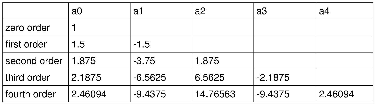
[00147] FIG. 33 illustrates the shaping functions of second, third and fourth order that are computed without constraint (iii) above. However, if constraint (iii) is applied, curves with a peak frequency deviation limited to different values can be obtained for each order by giving up one of the zero derivative constraints (ii).
[00148] The effect on eye pattern, correlation sidelobes, and spectral sidelobes may also be explored to determine shaping functions that may be better in a given application (such as exemplified by the raised cosine shape discussed herein). However, the over-exploration of different functions has limited merit because such a function will only be used for a limited number of samples per bit (e.g., 4, 8 or 16, and those 4, 8 or 16 values are going to be quantized to a limited number of bits of accuracy). When using N samples per bit, the spectrum is only defined out to +/- N/2 chiprates, and thus, small differences in the functions that cause higher or lower far-out spectral sidelobes may be masked by the time and value quantizations. Attention is thus turned to the effect of value quantization of the l,Q waveforms and methods to determine the best quantized values and how to digital-to- analog convert them.
[00149] When l,Q values of digital FM signals are computed to a high degree of accuracy, a
2 9
constant envelope will be maintained, namely I + Q = 1 . When however, the I and Q values are quantized to integer values less than some maximum value, such as +/- 31 for 6-bit quantizing, +/- 63 for 7-bit quantizing, or +/- 127 for 8-bit quantizing, it is not possible to guarantee that the squares of all pairs of integers sum to the same integer value, and thus, a constant envelope cannot be maintained exactly, and the quantized l,Q values will have both amplitude and phase errors. However, since the transmit power amplifier is hard limiting, the amplitude errors will be substantially shaved off, leaving only the phase errors. Therefore, in one exemplary embodiment, a higher priority when selecting quantized l,Q values is given to pairs of values that are closest in phase to the
unquantized vector without regard to amplitude error. Too much amplitude error may not be acceptable, but seeking pairs of quantized l,Q values (Kx,Ky) that are closest in phase angle, where Kx is within +/- 1 quantizing step of the closest quantizing to I and Ky is within +/- 1 quantizing step of the closest quantizing to Q, should give lower spectral sidelobes after hard limiting. This was confirmed to be so. However, there are low-pass filters (1060A,B) after the digital-to-analog converters (1050A,B) of FIG. 5 that alter the modified l,Q values, so it is necessary to compute the merit of this alternative quantization after these filters are included. This was done using Gaussian filters with a -3 dB cutoff point of 2 bitrates, and it was found that it was still beneficial to search for quantized values within +/-1 LSB that best matched the phase of l,Q.
[00150] Mathematically, integer values (Kx',Ky') within +/- 1 of (Kx,Ky) are sought for which:
2 2
[00151] (Kx7 Rk - I/R) + (Ky7 Rk - Q/R) is a minimum
2 2 2 2
[00152] where Rk = V(Kx' + Kx' ) and R = V(I + Q ).
[00153] The modified values (Κχ',Κν') were found to give lower spectral sidelobes after filters (1060A.B) and hard limiting in the transmit power amplifier.
[00154] Another practical imperfection that can give rise to elevated spectral sidelobes is digital-to-analog converter (DAC) accuracy. If the DAC does not give equal steps, this can result in additional quantizing noise. In particular, if a strong signal cancellation unit attempts to mimic the quantizing in the transmitter in order to maximize cancellation, the differences between the transmit DAC and the model used for cancellation will result in less effective cancellation. To mitigate this, a special form of DAC may be used that effectively guarantees equal quantizing steps in the mean, and this is briefly described below.
[00155] An exemplary 8-bit DAC (1050A.B) comprises 256 nominally equal current sources, each of which can be turned on and off by logic fed via an 8-bit value. When the 8-bit value is zero, no current sources are turned on, and when the 8-bit value is 255, 255 current sources are turned on (with one current source remaining turned off). In one exemplary embodiment, the 256 current sources are arranged in a ring, with those that are turned on occupying a first segment of the circle and those that are turned off occupying the other part of the circle. Whenever a new 8-bit value is received, it is first determined whether more current sources will be turned on, or whether current sources will be turned off. If more current sources are to be turned on, the additional one(s) of the currently OFF current sources clockwise of the ON segment are turned ON, while if fewer current sources are to be ON, then current sources counterclockwise of the currently ON segment are turned OFF. In this way, the ON segment of current sources and the OFF segment of current sources continuously rotate giving all current sources equal use in the mean for contributing to every desired analog value. Moreover, the time between a current turning on and off is maximized, thus reducing the effect of any speed limitations. In this way, the error spectrum in the mean is zero and is reduced for lower frequencies so that the error
power spectrum is quadratic rather than flat with reduced total net error power. In one exemplary embodiment, the digital-to-analog converter (DAC) is also balanced, like much of the rest of the high-frequency circuitry for the reasons mentioned above. A balanced DAC would transfer a current from a "+ output" to a "- output" in dependence on the digital value, thus providing a bipolar conversion with the digital value represented in the difference of the currents at the + and - outputs.
[00156] Other methods for optimizing the spectrum can be attempted when the number of samples per bit used to represent shaped digital FM signals is small. For example, at 4 samples per bit, if the vector is starting out at the 90 degree position [(l,Q) = (0,1 )] and heading for the 0 degree position [(l,Q) = (1 ,0)] in four steps, the first sample is (0.1 ), the middle sample, no. 3, is at 45 degrees (0.7071 ,0.7071 ), and the 5th sample is (1 ,0). Only samples 2 and 4 remain to be defined and symmetry dictates that sample 2 is the same angular displacement from 90 degrees as sample 4 is from 0 degrees. Therefore, there is only one variable that can be explored to reduce spectral sidelobes.
[00157] Alternatively, the sample instants can be displaced by half a sample either side of the +/- 90 and 0/180 points. The displacement is then a first variable and the angular position of the samples on either side of the 45 degree points is then a second variable. The spectrum can now be explored and optimized as a function of those two variables. The correlation function may be broader for this alternative, however, as the constellation points all depend on two bits and never only one.
[00158] Yet again, it can be beneficial if the vector dwells for two samples around each of the +/- 90 and 0/180 degree points. The latter case was investigated and the values optimized for best spectrum, giving the following l,Q values quantized to 8 bits accuracy are listed below:

[00160] When sampling as coarse as 4 samples per bit, it is necessary to have a sharper cutoff in the post DAC filters to suppress sidelobes beyond +/- 2 bitrates; for example, a Gaussian -3 dB cutoff in the region of 0.8 bitrates. Moreover, after hard limiting in the power amplifier, the correlation sidelobes were improved compared to using higher cutoff frequencies. The eye diagram, when using the above l,Q values, is illustrated in FIG. 35. The spectrum with a Gaussian post DAC filter BT factor of 0.8 is illustrated in FIG. 36, while the correlation sidelobes are illustrated in FIG. 37.
[00161] With 8 samples per bit, if the starting and ending sample values are as above at 90 degrees and 0 degrees respectively, then the middle sample 5 will be 45 degrees and samples 2, 3, and 4 will be at the same angles from 90 degrees, as samples 8, 6, and 7 will be from 0 degrees, so there are three variables to explore. Defining the quantity to be optimized, for example, as the total spectral energy beyond an exemplary +/-1 .5 bitrates, it is within the computational capabilities of a PC to explore this as a function of three variables within a reasonable time if so desired.
[00162] Several methods have been discussed for optimizing a constant envelope
modulation for use in a millimeter wave digital FMCW automotive radar with regard to the parameters that are important in such a system. The modulation is defined by a limited number of l,Q samples per bit, such as 4, 8, or 16, that are quantized in an optimum manner to a limited word length of, for example, 6, 7, or 8 bits. The l,Q samples are stored in memory (1030) from where they are recalled in dependence on the polarity of the modulation bits from a code generator, which may be precoded, and with regard to the current angular quadrant. Precoding and keeping track of the quadrant is performed by the state machine of l,Q selection logic (1020). The selected quantized l,Q samples are digital-to-analog converted using the above described analog-to-digital conversion techniques that shape the digital to analog quantization error noise to facilitate accurate subtraction of strong target echoes in the receiver by using a replica of the transmit modulator to generate a delayed, phase changed, and amplitude-weighted version that
best matches the signal to be subtracted. The digital-to-analog converted analog signals are low-pass filtered by post digital-to-analog filters (1060A,B) and then a radar carrier signal is quadrature modulated at a desired center or mean frequency. ] The exemplary embodiments disclosed herein cover many variations of constant envelope signals including GMSK, Raised Cosine shaped pulse-FM, and polynomial shaped pulse FM, and a person of normal skill in the art can derive many other variations using the principles exposed herein without departing from the spirit and scope of the invention as described by the attached claims.
Claims
1. A radar system for a vehicle, the radar system comprising:
at least one transmitter configured for installation and use on a vehicle;
wherein each of the at least one transmitter is configured to generate a sequence of chips at a selected chiprate, and wherein a modulation interval between successive chips is a reciprocal of the chiprate;
wherein each of the at least one transmitter is configured to generate a radio signal with a desired center frequency and to frequency modulate the radio signal using shaped frequency pulses to generate a frequency modulated radio signal, wherein the shaped frequency pulses correspond to a first signal, the frequency of which deviates from the desired center frequency during each of the modulation intervals according to a selected pulse shape, and wherein the selected pulse shape is determined by the generated sequence of chips;
wherein the at least one transmitter is configured to transmit the frequency modulated radio signal; and
at least one receiver configured for installation and use on the vehicle, and configured to receive the transmitted frequency modulated radio signal reflected from objects in the environment.
2. The radar system of Claim 1 , wherein each of the at least one transmitter comprises a frequency generator configured to generate the radio signal with the desired center frequency.
3. The radar system of Claim 2, wherein the frequency generator of the transmitter is configured to produce the first signal having a same center carrier frequency as the radio signal and having a constant relative phase.
4. The radar system of Claim 2, wherein the frequency generator is a carrier frequency generator.
5. The radar system of Claim 2, wherein the frequency generator comprises a quadrature local oscillator with provision for injection locking to a common sub-harmonic injection signal.
6. The radar system of Claim 1 , wherein each of the at least one transmitter comprises a code generator configured to generate the sequence of chips at the selected chiprate.
7. The radar system of Claim 6, wherein the code generators of each of the at least one transmitter are configured to produce different codes.
8. The radar system of Claim 1 , wherein each of the at least one transmitter comprises a power amplifier configured to amplify the modulated radio signal at a desired transmit power level.
9. The radar system of Claim 1 , wherein the power amplifier is a constant-envelope power amplifier.
10. The radar system of Claim 1 , wherein each of the at least one transmitter is coupled to an antenna to transmit the frequency modulated radio signal.
1 1 . The radar system of Claim 1 , wherein the radio signal is a carrier signal.
12. The radar system of Claim 1 , wherein each of the at least one transmitter comprises a modulator configured to frequency modulate the radio signal using the shaped frequency pulses.
13. The radar system of Claim 12, wherein the frequency of the radio signal deviates from the desired center frequency during each of the modulation intervals according to a selected pulse shape that is selected from a set of predetermined smooth frequency- deviation pulse shapes.
14. The radar system of Claim 13, wherein the modulator further comprises:
a waveform memory configured to store a number of precomputed I, Q waveforms, each precomputed at a number of samples for each of the modulation intervals, to correspond to a frequency modulated signal with one of the sets of predetermined smooth frequency-deviation pulse shapes;
waveform selection logic configured to select one of the precomputed I, Q waveforms depending on the current chip value and those of its neighbors, wherein the total number of neighboring values on which the selection depends corresponds in number and value with the values used for the precomputation of the selected I, Q waveform;
a digital-to-analog convertor configured to convert each I and Q samples of the selected I, Q waveform to corresponding analog I and Q signals; and
an I, Q modulator configured to modulate the radio signal with the analog I and Q signals to produce the frequency modulated radio signal.
15. The radar system of Claim 1 , wherein the desired center frequency is in a wave region of 70 to 80 GHz.
16. The radar system of Claim 1 , wherein pulse shapes are frequency deviation pulse shapes defined by a number of samples per each of the modulation intervals, and wherein an integral of each frequency deviation pulse shape over its entire impulse response length produces an incremental signal phase change of + 90 degrees.
17. The radar system of Claim 1 , wherein the selected pulse shape is determined by a limited number of successive ones of chips.
18. The radar system of Claim 17, wherein the limited number of successive ones of the chips which determine a selected pulse shape is a maximum of three.
19. The radar system of Claim 17, wherein the limited number of successive ones of the chips with determine a selected pulse shape is a maximum of two.
20. The radar system of Claim 1 , wherein the code generator produces a sequence of bits which is a maximum length sequence.
Applications Claiming Priority (6)
| Application Number | Priority Date | Filing Date | Title |
|---|---|---|---|
| US201662327003P | 2016-04-25 | 2016-04-25 | |
| US62/327,003 | 2016-04-25 | ||
| US201662382857P | 2016-09-02 | 2016-09-02 | |
| US62/382,857 | 2016-09-02 | ||
| US201762469165P | 2017-03-09 | 2017-03-09 | |
| US62/469,165 | 2017-03-09 |
Publications (2)
| Publication Number | Publication Date |
|---|---|
| WO2017187304A2 true WO2017187304A2 (en) | 2017-11-02 |
| WO2017187304A3 WO2017187304A3 (en) | 2017-12-14 |
Family
ID=60089482
Family Applications (2)
| Application Number | Title | Priority Date | Filing Date |
|---|---|---|---|
| PCT/IB2017/052279 WO2017187304A2 (en) | 2016-04-25 | 2017-04-20 | Digital frequency modulated continuous wave radar using handcrafted constant envelope modulation |
| PCT/IB2017/052373 WO2017187339A1 (en) | 2016-04-25 | 2017-04-25 | Vehicular radar system with self-interference cancellation |
Family Applications After (1)
| Application Number | Title | Priority Date | Filing Date |
|---|---|---|---|
| PCT/IB2017/052373 WO2017187339A1 (en) | 2016-04-25 | 2017-04-25 | Vehicular radar system with self-interference cancellation |
Country Status (2)
| Country | Link |
|---|---|
| US (3) | US9945935B2 (en) |
| WO (2) | WO2017187304A2 (en) |
Cited By (2)
| Publication number | Priority date | Publication date | Assignee | Title |
|---|---|---|---|---|
| US9945943B2 (en) | 2016-04-07 | 2018-04-17 | Uhnder, Inc. | Adaptive transmission and interference cancellation for MIMO radar |
| US10261179B2 (en) | 2016-04-07 | 2019-04-16 | Uhnder, Inc. | Software defined automotive radar |
Families Citing this family (47)
| Publication number | Priority date | Publication date | Assignee | Title |
|---|---|---|---|---|
| US9846228B2 (en) | 2016-04-07 | 2017-12-19 | Uhnder, Inc. | Software defined automotive radar systems |
| WO2017187304A2 (en) | 2016-04-25 | 2017-11-02 | Uhnder, Inc. | Digital frequency modulated continuous wave radar using handcrafted constant envelope modulation |
| WO2017187299A2 (en) | 2016-04-25 | 2017-11-02 | Uhnder, Inc. | Successive signal interference mitigation |
| US9791564B1 (en) | 2016-04-25 | 2017-10-17 | Uhnder, Inc. | Adaptive filtering for FMCW interference mitigation in PMCW radar systems |
| EP3449275A4 (en) | 2016-04-25 | 2020-01-01 | Uhnder, Inc. | Pmcw pmcw interference mitigation |
| US9791551B1 (en) | 2016-04-25 | 2017-10-17 | Uhnder, Inc. | Vehicular radar system with self-interference cancellation |
| US10573959B2 (en) | 2016-04-25 | 2020-02-25 | Uhnder, Inc. | Vehicle radar system using shaped antenna patterns |
| US9954955B2 (en) | 2016-04-25 | 2018-04-24 | Uhnder, Inc. | Vehicle radar system with a shared radar and communication system |
| US9753121B1 (en) | 2016-06-20 | 2017-09-05 | Uhnder, Inc. | Power control for improved near-far performance of radar systems |
| US11067667B2 (en) | 2016-09-08 | 2021-07-20 | Magna Closures Inc. | Radar detection system for non-contact human activation of powered closure member |
| US10934764B2 (en) | 2016-09-08 | 2021-03-02 | Magna Closures Inc. | Radar detection system for non-contact human activation of powered closure member |
| US9869762B1 (en) | 2016-09-16 | 2018-01-16 | Uhnder, Inc. | Virtual radar configuration for 2D array |
| US10908272B2 (en) | 2017-02-10 | 2021-02-02 | Uhnder, Inc. | Reduced complexity FFT-based correlation for automotive radar |
| US11454697B2 (en) | 2017-02-10 | 2022-09-27 | Uhnder, Inc. | Increasing performance of a receive pipeline of a radar with memory optimization |
| WO2018146632A1 (en) | 2017-02-10 | 2018-08-16 | Uhnder, Inc. | Radar data buffering |
| US10845477B2 (en) | 2017-05-10 | 2020-11-24 | Google Llc | Power management using a low-power radar |
| US10795009B2 (en) | 2017-05-31 | 2020-10-06 | Google Llc | Digital beamforming for radar sensing using wireless communication chipset |
| US10782390B2 (en) | 2017-05-31 | 2020-09-22 | Google Llc | Full-duplex operation for radar sensing using wireless communication chipset |
| US10754005B2 (en) | 2017-05-31 | 2020-08-25 | Google Llc | Radar modulation for radar sensing using a wireless communication chipset |
| DE102017209628A1 (en) * | 2017-06-08 | 2018-12-13 | Robert Bosch Gmbh | FMCW radar sensor for motor vehicles |
| US10914110B2 (en) | 2017-11-02 | 2021-02-09 | Magna Closures Inc. | Multifunction radar based detection system for a vehicle liftgate |
| US11105890B2 (en) | 2017-12-14 | 2021-08-31 | Uhnder, Inc. | Frequency modulated signal cancellation in variable power mode for radar applications |
| KR102455634B1 (en) * | 2018-01-22 | 2022-10-17 | 삼성전자주식회사 | Method and apparatus for determinig object distance using radar |
| DE102018109128B3 (en) | 2018-04-17 | 2019-10-02 | Infineon Technologies Ag | Radar receiver and method for receiving a radar signal |
| EP3588127B1 (en) | 2018-06-29 | 2024-02-14 | IMEC vzw | Spillover cancellation in radar systems |
| WO2020023673A1 (en) * | 2018-07-24 | 2020-01-30 | Smiths Interconnect, Inc. | Standoff detection system |
| US11054502B2 (en) * | 2018-07-26 | 2021-07-06 | Mercury Systems, Inc. | Method and system for intra-pulse frequency estimation against agile emitters |
| EP3620810B1 (en) * | 2018-09-05 | 2022-07-13 | Nxp B.V. | Radar interference detection |
| US10725175B2 (en) | 2018-10-30 | 2020-07-28 | United States Of America As Represented By The Secretary Of The Air Force | Method, apparatus and system for receiving waveform-diverse signals |
| US11474225B2 (en) * | 2018-11-09 | 2022-10-18 | Uhnder, Inc. | Pulse digital mimo radar system |
| DE102019200612A1 (en) * | 2019-01-18 | 2020-07-23 | Zf Friedrichshafen Ag | Device and method for calibrating a multiple-input-multiple-output radar sensor |
| US11487003B2 (en) | 2019-03-12 | 2022-11-01 | Ay Dee Kay Llc | Envelope regulation in a frequency-modulated continuous-wave radar system |
| WO2020183392A1 (en) | 2019-03-12 | 2020-09-17 | Uhnder, Inc. | Method and apparatus for mitigation of low frequency noise in radar systems |
| CN109831262B (en) * | 2019-03-28 | 2021-04-16 | 黄小花 | Intelligent low temperature stores up grain system signal calibration circuit |
| BR112021019115A2 (en) | 2019-05-20 | 2021-11-30 | Google Llc | Mobile device based radar system to provide a multi-mode interface and method for the same |
| KR20210132132A (en) | 2019-06-17 | 2021-11-03 | 구글 엘엘씨 | Mobile device-based radar system for applying different power modes to multi-mode interface |
| US11307299B2 (en) * | 2019-08-07 | 2022-04-19 | Apple Inc. | Radio frequency based sensing using communication signals |
| EP4045877A4 (en) * | 2019-10-17 | 2023-11-29 | Thales Canada Inc. | Portable positioning and odometry system |
| EP3819660A1 (en) * | 2019-11-05 | 2021-05-12 | NXP USA, Inc. | Radar transmitter module for digital modulation |
| CN111025276B (en) * | 2019-11-21 | 2022-04-05 | 南京航空航天大学 | Bistatic radar optimal radio frequency stealth power distribution method under frequency spectrum coexistence environment |
| US11796633B2 (en) * | 2019-12-16 | 2023-10-24 | Waymo Llc | Dynamic loading of radar unit configuration data based on changing radar parameters |
| EP3839561A1 (en) * | 2019-12-18 | 2021-06-23 | Imec VZW | Radar ranging |
| US11953615B2 (en) | 2020-01-13 | 2024-04-09 | Uhnder Inc. | Method and system for antenna array calibration for cross-coupling and gain/phase variations in radar systems |
| CN112162272B (en) * | 2020-09-11 | 2023-07-28 | 太原理工大学 | Radar ranging system based on true random number generator and ranging method thereof |
| CN112383494B (en) * | 2020-11-26 | 2022-10-28 | 西安烽火电子科技有限责任公司 | Burst communication receiving system based on DSSS-OQPSK |
| EP4262101A4 (en) * | 2020-12-23 | 2024-01-17 | Huawei Tech Co Ltd | Transmitter, radar and vehicle |
| CN112782663B (en) * | 2021-02-03 | 2023-07-21 | 海南大学 | Target parameter estimation method of FDA-MIMO radar under amplitude-phase error condition |
Family Cites Families (314)
| Publication number | Priority date | Publication date | Assignee | Title |
|---|---|---|---|---|
| US1882128A (en) | 1927-06-01 | 1932-10-11 | Edward W Fearing | Radiofrequency amplification system |
| US3374478A (en) | 1966-12-07 | 1968-03-19 | Spectronics Inc | Radar signaliing system with reduced clutter effect |
| US3735395A (en) | 1971-01-04 | 1973-05-22 | Iwatsu Electric Co Ltd | Projection type keyboard device |
| US3735398A (en) | 1971-05-20 | 1973-05-22 | Sperry Rand Corp | Base band short range pre-collision sensor for actuation of vehicle safety apparatus |
| US3750169A (en) | 1972-03-13 | 1973-07-31 | Sperry Rand Corp | Vehicular safety system |
| FR2220797B1 (en) * | 1973-03-06 | 1977-09-02 | Thomson Csf | |
| US4078234A (en) * | 1975-04-25 | 1978-03-07 | The United States Of America As Represented By The Secretary Of The Army | Continuous wave correlation radar system |
| US4176351A (en) * | 1978-08-18 | 1979-11-27 | Raytheon Company | Method of operating a continuous wave radar |
| US4566010A (en) | 1982-04-28 | 1986-01-21 | Raytheon Company | Processing arrangement for pulse compression radar |
| GB8527277D0 (en) | 1985-11-06 | 1985-12-11 | Formula Systems Ltd | Proximity detector |
| US4939685A (en) | 1986-06-05 | 1990-07-03 | Hughes Aircraft Company | Normalized frequency domain LMS adaptive filter |
| FR2751086A1 (en) | 1986-08-01 | 1998-01-16 | Thomson Csf | Mutual interference eliminating method for radar groups transmitting and receiving signals |
| US4882668A (en) | 1987-12-10 | 1989-11-21 | General Dynamics Corp., Pomona Division | Adaptive matched filter |
| US6121872A (en) | 1989-04-15 | 2000-09-19 | Bayerische Motoren Werke Ag | Object sensing device for motor vehicles |
| US5001486A (en) | 1989-08-04 | 1991-03-19 | Siemens-Albis | Radar system for determining the position of two or more objects |
| US5034906A (en) | 1990-03-30 | 1991-07-23 | Microwave Logic | Pseudorandom Binary Sequence delay systems |
| US5087918A (en) | 1990-04-02 | 1992-02-11 | Delco Electronics Corporation | FMCW/2FD implementation for vehicle near obstacle detection system |
| US5175710A (en) | 1990-12-14 | 1992-12-29 | Hutson William H | Multi-dimensional data processing and display |
| US5218619A (en) | 1990-12-17 | 1993-06-08 | Ericsson Ge Mobile Communications Holding, Inc. | CDMA subtractive demodulation |
| US5151702A (en) | 1991-07-22 | 1992-09-29 | General Electric Company | Complementary-sequence pulse radar with matched filtering following doppler filtering |
| US5508706A (en) | 1991-09-30 | 1996-04-16 | Trw Inc. | Radar signal processor |
| US5379322A (en) | 1992-01-07 | 1995-01-03 | Sanyo Electric Co., Ltd. | Baseband signal generator for digital modulator |
| US5272663A (en) | 1992-05-05 | 1993-12-21 | The Board Of Trustees Of The University Of Illinois | Apparatus and method for wide bandwidth adaptive filtering |
| US5302956A (en) | 1992-08-14 | 1994-04-12 | Vorad Safety Systems, Inc. | Multi-frequency, multi-target vehicular radar system using digital signal processing |
| US5280288A (en) | 1992-08-14 | 1994-01-18 | Vorad Safety Systems, Inc. | Interference avoidance system for vehicular radar system |
| AU667399B2 (en) | 1992-08-14 | 1996-03-21 | Vorad Safety Systems, Inc. | Recording of operational events in an automotive vehicle |
| US5341141A (en) | 1993-03-09 | 1994-08-23 | Hughes Missile Systems Company | Three dimensional imaging radar |
| US5345470A (en) | 1993-03-31 | 1994-09-06 | Alexander Richard O | Methods of minimizing the interference between many multiple FMCW radars |
| US5376939A (en) | 1993-06-21 | 1994-12-27 | Martin Marietta Corporation | Dual-frequency, complementary-sequence pulse radar |
| US5654890A (en) | 1994-05-31 | 1997-08-05 | Lockheed Martin | High resolution autonomous precision approach and landing system |
| US5657021A (en) | 1994-06-30 | 1997-08-12 | Ehsani Engineering Enterprises, Inc. | System and method for radar-vision for vehicles in traffic |
| US5724041A (en) * | 1994-11-24 | 1998-03-03 | The Furukawa Electric Co., Ltd. | Spread spectrum radar device using pseudorandom noise signal for detection of an object |
| JP3302849B2 (en) | 1994-11-28 | 2002-07-15 | 本田技研工業株式会社 | Automotive radar module |
| US5497162A (en) | 1995-01-09 | 1996-03-05 | Northrop Grumman Corporation | Radar signal selection based upon antenna bearing |
| JP2885269B2 (en) | 1995-02-01 | 1999-04-19 | 日本電気株式会社 | Adaptive control filter |
| US5570093A (en) | 1995-02-10 | 1996-10-29 | Applied Concepts, Inc. | Police traffic radar using absolute signal strength information to improve target signal processing accuracy |
| US5917430A (en) | 1995-08-28 | 1999-06-29 | The Safety Warning System, L.C. | Radar based highway safety warning system |
| US5654715A (en) | 1995-12-15 | 1997-08-05 | Honda Giken Kogyo Kabushiki Kaisha | Vehicle-surroundings monitoring apparatus |
| US5847661A (en) | 1996-03-15 | 1998-12-08 | Intelligent Ideation, Inc. | Vehicle data acquisition system |
| US5959571A (en) * | 1996-04-22 | 1999-09-28 | The Furukawa Electric Co., Ltd. | Radar device |
| US5970400A (en) | 1996-04-30 | 1999-10-19 | Magellan Corporation | Adjusting the timing and synchronization of a radio's oscillator with a signal from an SATPS satellite |
| US5657023A (en) | 1996-05-02 | 1997-08-12 | Hughes Electronics | Self-phase up of array antennas with non-uniform element mutual coupling and arbitrary lattice orientation |
| GB9611800D0 (en) | 1996-06-06 | 1996-08-07 | Univ Bristol | Post-reception focusing in remote detection systems |
| JP3441301B2 (en) | 1996-07-10 | 2003-09-02 | 株式会社東芝 | Receiver and synchronization acquisition circuit |
| EP0932837B1 (en) | 1996-10-17 | 2012-07-25 | Saab AB | Procedure for the elimination of interference in a radar unit of the fmcw type |
| US5892477A (en) | 1996-11-13 | 1999-04-06 | Trw Inc. | Anti-jam FM/CW radar |
| US6900775B2 (en) | 1997-03-03 | 2005-05-31 | Celletra Ltd. | Active antenna array configuration and control for cellular communication systems |
| GB9718321D0 (en) | 1997-09-01 | 1997-11-05 | Cambridge Consultants | Electromagnetic sensor system |
| US5931893A (en) | 1997-11-11 | 1999-08-03 | Ericsson, Inc. | Efficient correlation over a sliding window |
| US6363105B1 (en) | 1998-02-17 | 2002-03-26 | Ericsson Inc. | Flexible sliding correlator for direct sequence spread spectrum systems |
| US6069581A (en) | 1998-02-20 | 2000-05-30 | Amerigon | High performance vehicle radar system |
| US6400308B1 (en) | 1998-02-20 | 2002-06-04 | Amerigon Inc. | High performance vehicle radar system |
| US6151366A (en) | 1998-04-17 | 2000-11-21 | Advanced Microdevices, Inc. | Method and apparatus for modulating signals |
| EP1367670B1 (en) | 1998-07-13 | 2006-09-06 | NTT Mobile Communications Network Inc. | Calibration for an adaptive array antenna |
| DE69928735T2 (en) | 1998-09-14 | 2006-07-06 | Kabushiki Kaisha Toyota Chuo Kenkyusho, Nagakute | Holographic radar |
| US6417796B1 (en) | 1998-09-16 | 2002-07-09 | Mph Industries, Inc. | Doppler-based traffic radar system |
| GB2342251A (en) | 1998-09-29 | 2000-04-05 | Secr Defence | Proximity measuring apparatus |
| US6184829B1 (en) | 1999-01-08 | 2001-02-06 | Trueposition, Inc. | Calibration for wireless location system |
| JP4035252B2 (en) | 1999-02-04 | 2008-01-16 | 本田技研工業株式会社 | Radar equipment |
| US6307622B1 (en) | 1999-02-17 | 2001-10-23 | Infineon Technologies North America Corp. | Correlation based optical ranging and proximity detector |
| JP2000292538A (en) | 1999-04-07 | 2000-10-20 | Mitsubishi Electric Corp | Obstacle detector for vehicle |
| DE19922411A1 (en) * | 1999-04-07 | 2000-10-12 | Volkswagen Ag | Radar measurement of distances, relative speeds between vehicle, obstruction(s) involves computing intercepts of all lines from 2 chirps at 2 frequency positions in distance-speed diagram |
| US20030102997A1 (en) | 2000-02-13 | 2003-06-05 | Hexagon System Engineering Ltd. | Vehicle communication network |
| JP3703689B2 (en) | 2000-06-01 | 2005-10-05 | 三菱電機株式会社 | Obstacle detection device and obstacle detection system |
| US6768391B1 (en) | 2000-06-22 | 2004-07-27 | Ericsson Inc. | Class-B biased gilbert cells and quadrature modulators |
| US6714956B1 (en) | 2000-07-24 | 2004-03-30 | Via Technologies, Inc. | Hardware accelerator for normal least-mean-square algorithm-based coefficient adaptation |
| JP5063851B2 (en) | 2000-08-16 | 2012-10-31 | ヴァレオ・レイダー・システムズ・インコーポレーテッド | Proximity object detection system |
| AU2001286513A1 (en) | 2000-08-16 | 2002-02-25 | Raytheon Company | Switched beam antenna architecture |
| US6707419B2 (en) | 2000-08-16 | 2004-03-16 | Raytheon Company | Radar transmitter circuitry and techniques |
| US8989920B2 (en) | 2000-09-08 | 2015-03-24 | Intelligent Technologies International, Inc. | Travel information sensing and communication system |
| US6834291B1 (en) | 2000-10-27 | 2004-12-21 | Intel Corporation | Gold code generator design |
| GB0027238D0 (en) | 2000-11-08 | 2000-12-27 | Secr Defence | Adaptive filter |
| US6865218B1 (en) | 2000-11-27 | 2005-03-08 | Ericsson Inc. | Multipath interference reduction for a CDMA system |
| DE10059673A1 (en) | 2000-12-01 | 2002-06-06 | Bosch Gmbh Robert | Pulse radar method as well as pulse radar sensor and system |
| US6683560B2 (en) | 2000-12-29 | 2004-01-27 | Honeywell International Inc. | System and technique for enhanced radar object detection |
| DE10108582A1 (en) | 2001-02-22 | 2002-09-05 | Bosch Gmbh Robert | Method for detecting disturbed states of a radar device and radar device |
| US6449169B1 (en) | 2001-02-28 | 2002-09-10 | Siliconware Precision Industries Co., Ltd. | Ball grid array package with interdigitated power ring and ground ring |
| US20020155811A1 (en) | 2001-04-18 | 2002-10-24 | Jerry Prismantas | System and method for adapting RF transmissions to mitigate the effects of certain interferences |
| JP3651430B2 (en) | 2001-09-17 | 2005-05-25 | 日本電気株式会社 | Array antenna calibration apparatus and calibration method |
| US6624611B2 (en) | 2001-10-30 | 2003-09-23 | Taw Security Concepts, Inc. | Sensing vehicle battery charging and/or engine block heating to trigger pre-heating of a mobile electronic device |
| US7006587B1 (en) | 2001-11-20 | 2006-02-28 | Cisco Technolgy, Inc. | Preamble aided synchronization |
| JP2003218621A (en) | 2002-01-21 | 2003-07-31 | Nec Corp | Apparatus and method for calibrating array antenna |
| US6583753B1 (en) | 2002-04-03 | 2003-06-24 | Delphi Technologies, Inc. | Vehicle back-up and parking aid radar system |
| US6674908B1 (en) | 2002-05-04 | 2004-01-06 | Edward Lasar Aronov | Method of compression of binary data with a random number generator |
| US7119739B1 (en) | 2002-05-14 | 2006-10-10 | Bae Systems Information And Electronic Systems Integration Inc. | Near field to far field DF antenna array calibration technique |
| AU2003250755A1 (en) | 2002-06-18 | 2003-12-31 | Automotive Distance Control Systems Gmbh | Circuit arrangement for generating an iq signal |
| US6961423B2 (en) | 2002-06-24 | 2005-11-01 | Freescale Semiconductor, Inc. | Method and apparatus for performing adaptive filtering |
| US7433908B2 (en) | 2002-07-16 | 2008-10-07 | Tellabs Operations, Inc. | Selective-partial-update proportionate normalized least-mean-square adaptive filtering for network echo cancellation |
| US6873251B2 (en) | 2002-07-16 | 2005-03-29 | Delphi Technologies, Inc. | Tracking system and method employing multiple overlapping sensors |
| DE10241463A1 (en) | 2002-09-06 | 2004-03-18 | Robert Bosch Gmbh | Radar measurement equipment for vehicle, differentiates between first and second returns generated from two radar emissions at different frequencies |
| JP3885716B2 (en) | 2002-11-21 | 2007-02-28 | 日産自動車株式会社 | Recommended operation amount generator for vehicles |
| DE10254982A1 (en) | 2002-11-26 | 2004-06-03 | Robert Bosch Gmbh | Method and device for adaptive power control |
| JP2004216954A (en) | 2003-01-10 | 2004-08-05 | Hitachi Ltd | Traveling control device for vehicle |
| JP3785542B2 (en) | 2003-02-25 | 2006-06-14 | よこはまティーエルオー株式会社 | Pulse waveform generation method |
| KR100498965B1 (en) | 2003-04-22 | 2005-07-01 | 삼성전자주식회사 | A System and Method For Communicating Vehicle Driving Information Using Ad Hoc Network |
| US6975246B1 (en) | 2003-05-13 | 2005-12-13 | Itt Manufacturing Enterprises, Inc. | Collision avoidance using limited range gated video |
| EP1496371A1 (en) | 2003-07-07 | 2005-01-12 | Mitsubishi Electric Information Technology Centre Europe B.V. | Generation of packets of waveforms |
| CA2452945C (en) | 2003-09-23 | 2016-05-10 | Mcmaster University | Binaural adaptive hearing system |
| JP4318529B2 (en) | 2003-10-24 | 2009-08-26 | 富士通株式会社 | Communications system |
| JP4198034B2 (en) | 2003-11-25 | 2008-12-17 | 富士通株式会社 | Information code transmitter |
| US20050156780A1 (en) | 2004-01-16 | 2005-07-21 | Ghz Tr Corporation | Methods and apparatus for automotive radar sensors |
| US20060262007A1 (en) | 2004-01-16 | 2006-11-23 | Clariant Technologies, Corp. | Methods and apparatus for automotive radar sensors |
| DE102004004492A1 (en) | 2004-01-29 | 2005-08-18 | Robert Bosch Gmbh | Radar system for motor vehicles |
| US20050201457A1 (en) | 2004-03-10 | 2005-09-15 | Allred Daniel J. | Distributed arithmetic adaptive filter and method |
| DE102004026182A1 (en) | 2004-05-28 | 2005-12-22 | Robert Bosch Gmbh | Method for reducing noise influences on a high-frequency measuring device, and high-frequency measuring device |
| JP2006003303A (en) | 2004-06-21 | 2006-01-05 | Fujitsu Ten Ltd | Radar device |
| GB2415560A (en) | 2004-06-25 | 2005-12-28 | Instro Prec Ltd | Vehicle safety system having a combined range finding means and a communication means |
| JP4551145B2 (en) | 2004-07-13 | 2010-09-22 | 富士通株式会社 | Radar apparatus and radar apparatus control method |
| CN1985187B (en) | 2004-07-16 | 2012-05-16 | 富士通天株式会社 | Monopulse radar apparatus and antenna switch |
| KR20070089119A (en) | 2004-07-23 | 2007-08-30 | 와이어리스 밸리 커뮤니케이션 인크 | System, method, and apparatus for determining and using the position of wireless devices or infrastructure for wireless network enhancements |
| US7338450B2 (en) | 2004-08-27 | 2008-03-04 | General Electric Company | Method and apparatus for performing CW doppler ultrasound utilizing a 2D matrix array |
| US7395363B2 (en) | 2004-09-09 | 2008-07-01 | Intel Corporation | Methods and apparatus for multiple bit rate serial communication |
| DE102004044120A1 (en) | 2004-09-13 | 2006-03-16 | Robert Bosch Gmbh | Antenna structure for series-fed planar antenna elements |
| US7420503B2 (en) | 2004-10-14 | 2008-09-02 | Anritsu Corporation | Small-sized low-power dissipation short-range radar that can arbitrarily change delay time between transmission and reception with high time resolution and method of controlling the same |
| DE102004052518A1 (en) | 2004-10-29 | 2006-05-04 | Robert Bosch Gmbh | Device and method for the angular resolution of distance and speed of an object |
| JP2006135674A (en) | 2004-11-05 | 2006-05-25 | Ntt Docomo Inc | Receiver for mobile communication, transmitter for mobile communication, reception method for mobile communication, and transmission method for mobile communication |
| US7123169B2 (en) | 2004-11-16 | 2006-10-17 | Northrop Grumman Corporation | Method and apparatus for collaborative aggregate situation awareness |
| DE102004059915A1 (en) | 2004-12-13 | 2006-06-14 | Robert Bosch Gmbh | radar system |
| US7683827B2 (en) | 2004-12-15 | 2010-03-23 | Valeo Radar Systems, Inc. | System and method for reducing the effect of a radar interference signal |
| US7395084B2 (en) | 2005-01-24 | 2008-07-01 | Sikorsky Aircraft Corporation | Dynamic antenna allocation system |
| JP4462060B2 (en) | 2005-02-14 | 2010-05-12 | 株式会社デンソー | FMCW radar equipment |
| US7642952B2 (en) | 2005-03-31 | 2010-01-05 | Panasonic Corporation | Spread spectrum radar apparatus |
| JP4747652B2 (en) | 2005-04-15 | 2011-08-17 | 株式会社デンソー | FMCW radar |
| WO2006120823A1 (en) | 2005-05-13 | 2006-11-16 | Murata Manufacturing Co., Ltd. | Radar |
| WO2006123499A1 (en) | 2005-05-16 | 2006-11-23 | Murata Manufacturing Co., Ltd. | Radar |
| JP4478606B2 (en) | 2005-05-19 | 2010-06-09 | 富士通株式会社 | Calibration apparatus and calibration method for linear array antenna |
| JP4923439B2 (en) | 2005-05-20 | 2012-04-25 | 株式会社デンソー | Radar interference suppression method |
| WO2006133268A2 (en) | 2005-06-06 | 2006-12-14 | Signal Labs, Inc. | System and method for detection and discrimination of targets in the presence of interference |
| JP2007003305A (en) | 2005-06-22 | 2007-01-11 | Matsushita Electric Ind Co Ltd | Spread spectrum radar device |
| US7277046B2 (en) | 2005-07-08 | 2007-10-02 | Raytheon Company | Single transmit multi-receiver modulation radar, multi-modulation receiver and method |
| US8169890B2 (en) | 2005-07-20 | 2012-05-01 | Qualcomm Incorporated | Systems and method for high data rate ultra wideband communication |
| EP1777546B1 (en) | 2005-10-24 | 2010-05-26 | Mitsubishi Electric Information Technology Centre Europe B.V. | Object detection |
| TWI287514B (en) | 2005-11-03 | 2007-10-01 | Ind Tech Res Inst | Inter-vehicle communication and warning apparatus |
| JP2007132768A (en) | 2005-11-10 | 2007-05-31 | Hitachi Ltd | Vehicle-mounted radar system having communications function |
| US7400290B2 (en) | 2005-12-30 | 2008-07-15 | Valeo Raytheon Systems, Inc. | Vehicle radar system having multiple operating modes |
| US20070152872A1 (en) | 2005-12-30 | 2007-07-05 | Woodington Walter G | Reducing undesirable coupling of signal(s) between two or more signal paths in a radar system |
| US7791530B2 (en) | 2006-01-05 | 2010-09-07 | Autoliv Asp, Inc. | Time duplex apparatus and method for radar sensor front-ends |
| US20070171122A1 (en) | 2006-01-25 | 2007-07-26 | Fujitsu Ten Limited | Radar apparatus and interference detection method |
| US20070182623A1 (en) | 2006-02-03 | 2007-08-09 | Shuqing Zeng | Method and apparatus for on-vehicle calibration and orientation of object-tracking systems |
| JP5226185B2 (en) | 2006-02-15 | 2013-07-03 | 富士通株式会社 | Detecting and ranging device |
| JP2007232498A (en) * | 2006-02-28 | 2007-09-13 | Hitachi Ltd | Obstacle detecting system |
| US8059026B1 (en) | 2006-03-01 | 2011-11-15 | The United States Of America As Represented By The Secretary Of The Air Force | Interference avoiding transform domain radar |
| JP4994239B2 (en) * | 2006-04-04 | 2012-08-08 | パナソニック株式会社 | Code generator |
| US7830982B2 (en) | 2006-05-12 | 2010-11-09 | Northrop Grumman Systems Corporation | Common antenna array using baseband adaptive beamforming and digital IF conversion |
| WO2007146560A2 (en) | 2006-05-24 | 2007-12-21 | Clariant Technologies Corp. | Methods and apparatus for hyperview automotive radar |
| US7460055B2 (en) * | 2006-06-02 | 2008-12-02 | Panasonic Corporation | Radar apparatus |
| JP4275694B2 (en) | 2006-10-27 | 2009-06-10 | 三菱電機株式会社 | Radar equipment |
| US8072370B2 (en) | 2006-10-31 | 2011-12-06 | Valeo Radar Systems, Inc. | System and method for generating an alert signal in a detection system |
| JP4994023B2 (en) | 2006-12-25 | 2012-08-08 | 富士重工業株式会社 | Pulse radar, automotive radar and landing assist radar |
| JP5130034B2 (en) | 2006-12-27 | 2013-01-30 | 株式会社デンソーアイティーラボラトリ | Electronic scanning radar equipment |
| EP3624086A1 (en) | 2007-01-25 | 2020-03-18 | Magna Electronics Inc. | Radar sensing system for vehicle |
| JP2008249693A (en) | 2007-03-02 | 2008-10-16 | Matsushita Electric Ind Co Ltd | Spread spectrum type radar device |
| JP4492628B2 (en) | 2007-03-20 | 2010-06-30 | 株式会社デンソー | Interference judgment method, FMCW radar |
| JP4356758B2 (en) | 2007-03-20 | 2009-11-04 | 株式会社デンソー | FMCW radar |
| JP5160114B2 (en) | 2007-03-26 | 2013-03-13 | 本田技研工業株式会社 | Vehicle passage judgment device |
| US7724180B2 (en) | 2007-05-04 | 2010-05-25 | Toyota Motor Corporation | Radar system with an active lens for adjustable field of view |
| US7609198B2 (en) | 2007-05-21 | 2009-10-27 | Spatial Digital Systems, Inc. | Apparatus and method for radar imaging by measuring spatial frequency components |
| JP4476315B2 (en) | 2007-08-17 | 2010-06-09 | 三菱電機株式会社 | In-vehicle radar system |
| DE102007039897B3 (en) | 2007-08-23 | 2008-10-16 | Universität Karlsruhe (Th) | A method of operating an antenna array with multiple transmitters and multiple receivers and associated apparatus |
| JP4470978B2 (en) | 2007-08-30 | 2010-06-02 | トヨタ自動車株式会社 | Receiving apparatus and wireless communication system |
| JP2009069022A (en) * | 2007-09-13 | 2009-04-02 | Panasonic Corp | Radar device, its control method and vehicle |
| US20090072957A1 (en) | 2007-09-14 | 2009-03-19 | Honeywell International Inc. | Radio frequency proximity sensor and sensor system |
| JP2009074856A (en) * | 2007-09-19 | 2009-04-09 | Panasonic Corp | Spread spectrum radar system |
| JP2009080024A (en) | 2007-09-26 | 2009-04-16 | Fujitsu Ltd | Detection and ranging apparatus and method |
| US9282945B2 (en) | 2009-04-14 | 2016-03-15 | Maui Imaging, Inc. | Calibration of ultrasound probes |
| JP4974168B2 (en) | 2007-10-02 | 2012-07-11 | 古河電気工業株式会社 | Radar system antenna |
| US9966989B2 (en) | 2007-10-17 | 2018-05-08 | Applied Radar, Inc. | Array antenna system and spread spectrum beamformer method |
| JP5478010B2 (en) | 2007-11-12 | 2014-04-23 | 株式会社デンソーアイティーラボラトリ | Electronic scanning radar equipment |
| US7812758B2 (en) * | 2007-11-27 | 2010-10-12 | Northrop Grumman Space And Mission Systems Corporation | Synthetic aperture radar (SAR) imaging system |
| DE102007061383A1 (en) | 2007-12-19 | 2009-06-25 | Robert Bosch Gmbh | Method for operating an electrical device and electrical device |
| WO2009081981A1 (en) | 2007-12-25 | 2009-07-02 | Honda Elesys Co., Ltd. | Electronic scanning radar apparatus, received wave direction estimating method, and received wave direction estimating program |
| US8026843B2 (en) | 2008-01-31 | 2011-09-27 | Infineon Technologies Ag | Radar methods and systems using ramp sequences |
| WO2009099952A2 (en) | 2008-02-01 | 2009-08-13 | Viasat, Inc. | Highly integrated circuit architecture |
| JP4569652B2 (en) | 2008-03-21 | 2010-10-27 | 株式会社デンソー | Recognition system |
| US20090254260A1 (en) | 2008-04-07 | 2009-10-08 | Axel Nix | Full speed range adaptive cruise control system |
| JP2009265007A (en) | 2008-04-28 | 2009-11-12 | Hitachi Ltd | Mobile radar and planar antenna |
| US8582622B2 (en) | 2008-05-11 | 2013-11-12 | Qualcomm Incorporated | Spread-spectrum coding of data bursts |
| US8049663B2 (en) | 2008-05-21 | 2011-11-01 | Raytheon Company | Hardware compensating pulse compression filter system and method |
| EP2131209A1 (en) | 2008-06-03 | 2009-12-09 | Saab Ab | A radar receiver and a method for processing radar returns |
| DE102008038365A1 (en) | 2008-07-02 | 2010-01-07 | Adc Automotive Distance Control Systems Gmbh | Vehicle radar system and method for determining a position of at least one object relative to a vehicle |
| US8272281B2 (en) | 2008-11-11 | 2012-09-25 | Fisher Controls International, Llc | Remotely readable valve position indicators |
| US7791528B2 (en) | 2008-11-24 | 2010-09-07 | Autoliv Asp, Inc. | Method and apparatus for radar signal processing |
| EP2374217B1 (en) | 2008-12-09 | 2013-04-10 | Telefonaktiebolaget L M Ericsson (PUBL) | Cross-coupling interference cancellation in multiple receive branches with independent demodulation signals |
| KR101159887B1 (en) | 2008-12-22 | 2012-06-26 | 창원대학교 산학협력단 | Band-pass sampling receiver and method for receiving of the same |
| US8229663B2 (en) | 2009-02-03 | 2012-07-24 | GM Global Technology Operations LLC | Combined vehicle-to-vehicle communication and object detection sensing |
| WO2010095946A1 (en) | 2009-02-20 | 2010-08-26 | Nederlandse Organisatie Voor Toegepast-Natuurwetenschappelijk Onderzoek Tno | A method of detecting a scatterer in a structure, a radar system and a computer program product |
| DE102009001265A1 (en) | 2009-03-02 | 2010-09-09 | Robert Bosch Gmbh | Radar sensor with Blinheitserkennungseinrichtung |
| US7969349B2 (en) | 2009-04-06 | 2011-06-28 | Raytheon Company | System and method for suppressing close clutter in a radar system |
| DE112010001529A5 (en) | 2009-04-06 | 2012-10-25 | Conti Temic Microelectronic Gmbh | RADAR SYSTEM WITH ARRANGEMENTS AND METHOD FOR DECOUPLING TRANSMISSION AND RECEPTION SIGNALS AND SUPPRESSING NOISE EMISSIONS |
| JP2010261784A (en) * | 2009-05-01 | 2010-11-18 | Denso Corp | Radar apparatus |
| US8836601B2 (en) | 2013-02-04 | 2014-09-16 | Ubiquiti Networks, Inc. | Dual receiver/transmitter radio devices with choke |
| US8207887B2 (en) | 2009-06-19 | 2012-06-26 | The United States Of America As Represented By The Secretary Of The Army | Computationally efficent radar processing method and sytem for SAR and GMTI on a slow moving platform |
| US8912950B2 (en) | 2009-08-03 | 2014-12-16 | Raytheon Company | Interference mitigation in through the wall radar |
| EP2513666B1 (en) | 2009-12-18 | 2015-02-18 | L-3 Communications Cyterra Corporation | Moving entity detection |
| US8188908B2 (en) | 2010-01-29 | 2012-05-29 | Amtech Systems, LLC | System and method for measurement of distance to a tag by a modulated backscatter RFID reader |
| CN102742073B (en) | 2010-02-08 | 2015-04-15 | 瑞典爱立信有限公司 | An antenna with adjustable beam characteristics |
| US8600606B2 (en) | 2010-02-11 | 2013-12-03 | GM Global Technology Operations LLC | Vehicle safety systems and methods |
| EP2537309B1 (en) | 2010-02-15 | 2013-10-23 | Telefonaktiebolaget L M Ericsson (publ) | Method and apparatus providing protection and dc balance in a communication system |
| CN102893173B (en) | 2010-03-05 | 2014-12-03 | 温莎大学 | Radar system and method of manufacturing same |
| EP2545392B1 (en) | 2010-03-08 | 2013-12-25 | Nederlandse Organisatie voor toegepast- natuurwetenschappelijk onderzoek TNO | A method of compensating sub-array or element failure in a phased array radar system, a phased array radar system and a computer program product |
| US8427371B2 (en) | 2010-04-09 | 2013-04-23 | Raytheon Company | RF feed network for modular active aperture electronically steered arrays |
| US8330650B2 (en) | 2010-05-07 | 2012-12-11 | The United States Of America, As Represented By The Secretary Of The Army | Radar system and antenna with delay lines and method thereof |
| US8102306B2 (en) | 2010-05-13 | 2012-01-24 | The United States Of America As Represented By The Secretary Of The Navy | Active-radar-assisted passive composite imagery for aiding navigation or detecting threats |
| US8259003B2 (en) | 2010-05-14 | 2012-09-04 | Massachusetts Institute Of Technology | High duty cycle radar with near/far pulse compression interference mitigation |
| EP2390679B1 (en) | 2010-05-27 | 2012-10-03 | Mitsubishi Electric R&D Centre Europe B.V. | Automotive radar with radio-frequency interference avoidance |
| IL206008A0 (en) | 2010-05-27 | 2011-02-28 | Amir Meir Zilbershtain | Transmit receive interference cancellation |
| US8879378B2 (en) | 2010-05-28 | 2014-11-04 | Selim Shlomo Rakib | Orthonormal time-frequency shifting and spectral shaping communications method |
| US20110291874A1 (en) | 2010-06-01 | 2011-12-01 | De Mersseman Bernard | Vehicle radar system and method for detecting objects |
| JP5093298B2 (en) | 2010-06-04 | 2012-12-12 | 株式会社デンソー | Direction detection device |
| WO2012008110A1 (en) | 2010-07-16 | 2012-01-19 | パナソニック株式会社 | Radar device |
| CN102763001B (en) | 2010-08-09 | 2014-08-20 | 松下电器产业株式会社 | Radar imaging device, imaging method and program therefor |
| JP5842143B2 (en) | 2010-09-02 | 2016-01-13 | パナソニックIpマネジメント株式会社 | Radar equipment |
| JP5535024B2 (en) | 2010-10-07 | 2014-07-02 | パナソニック株式会社 | Radar equipment |
| US8624773B2 (en) | 2010-11-09 | 2014-01-07 | The United States Of America As Represented By The Secretary Of The Army | Multidirectional target detecting system and method |
| US8432309B2 (en) | 2010-11-29 | 2013-04-30 | Freescale Semiconductor, Inc. | Automotive radar system and method for using same |
| DE102010064346A1 (en) | 2010-12-29 | 2012-07-05 | Robert Bosch Gmbh | Radar sensor for motor vehicles |
| KR101206000B1 (en) | 2010-12-31 | 2012-11-28 | 전자부품연구원 | Variable order short-term predictor |
| US9331765B2 (en) | 2011-02-01 | 2016-05-03 | Blackberry Limited | Mixed rank downlink multi-user interference alignment scheme |
| US8629799B2 (en) | 2011-03-30 | 2014-01-14 | Sandia Research Corporation | Surface penetrating radar system and target zone investigation methodology |
| CA2773716C (en) | 2011-04-08 | 2018-01-02 | Her Majesty The Queen In Right Of Canada, As Represented By The Minister Of Industry Through The Communications Research Centre Canada | Method and system for wireless data communication |
| WO2012149869A1 (en) | 2011-05-03 | 2012-11-08 | 国民技术股份有限公司 | Communication method, communication device and communication system |
| US9121943B2 (en) | 2011-05-23 | 2015-09-01 | Sony Corporation | Beam forming device and method |
| JP5938737B2 (en) | 2011-06-01 | 2016-06-22 | パナソニックIpマネジメント株式会社 | Radar equipment |
| US8750350B2 (en) | 2011-07-15 | 2014-06-10 | Broadcom Corporation | Transmitter with a variable sampling rate |
| DE102011079615A1 (en) | 2011-07-22 | 2013-01-24 | Robert Bosch Gmbh | FMCW radar system and interference detection method for FMCW radar systems |
| US9372259B2 (en) | 2011-08-12 | 2016-06-21 | Panasonic Corporation | Radar apparatus |
| US8422540B1 (en) | 2012-06-21 | 2013-04-16 | CBF Networks, Inc. | Intelligent backhaul radio with zero division duplexing |
| JP5866917B2 (en) | 2011-09-20 | 2016-02-24 | 富士通株式会社 | Detecting and ranging apparatus and detecting and ranging method |
| DE102011055693A1 (en) | 2011-11-24 | 2013-05-29 | Hella Kgaa Hueck & Co. | Radar apparatus and method for detecting a failure of a receiving channel of a radar device |
| US9535151B2 (en) | 2011-12-28 | 2017-01-03 | Hrl Laboratories, Llc | Coded aperture beam analysis method and apparatus |
| US20130169468A1 (en) | 2011-12-30 | 2013-07-04 | Flir Systems, Inc. | Radar system and related methods |
| US8587464B2 (en) | 2012-01-09 | 2013-11-19 | International Business Machines Corporation | Off-line gain calibration in a time-interleaved analog-to-digital converter |
| US9116227B2 (en) | 2012-02-22 | 2015-08-25 | Toyota Motor Engineering & Manufacturing North America, Inc. | Hybrid radar integrated into single package |
| JP5993441B2 (en) | 2012-03-02 | 2016-09-14 | 東京計器株式会社 | Radar apparatus and radar signal processing method |
| US9172476B2 (en) | 2012-03-09 | 2015-10-27 | The United States Of America As Represented By The Secretary Of The Army | Method and system for removal of noise in signal |
| US8694306B1 (en) | 2012-05-04 | 2014-04-08 | Kaonyx Labs LLC | Systems and methods for source signal separation |
| ITTO20120417A1 (en) * | 2012-05-09 | 2013-11-10 | St Microelectronics Srl | PROCEDURE AND DEVICES FOR DEVELOPING RADAR SIGNALS, FOR EXAMPLE FOR ROAD SAFETY SYSTEMS, ITS RELATED PRODUCT |
| US20130314271A1 (en) | 2012-05-25 | 2013-11-28 | Brandt Braswell | Vehicle-borne radar systems with continuous-time, sigma delta analog-to-digital converters, and methods of their operation |
| JP6190140B2 (en) | 2012-06-21 | 2017-08-30 | 古野電気株式会社 | Target detection apparatus and target detection method |
| US9140782B2 (en) | 2012-07-23 | 2015-09-22 | Google Technology Holdings LLC | Inter-vehicle alert system with nagable video look ahead |
| US9297885B2 (en) | 2012-07-27 | 2016-03-29 | Honeywell International Inc. | Method of system compensation to reduce the effects of self interference in frequency modulated continuous wave altimeter systems |
| DE102012015250A1 (en) | 2012-08-01 | 2014-02-06 | Audi Ag | Radar sensor for a motor vehicle, motor vehicle and communication method |
| US9000974B2 (en) * | 2012-09-10 | 2015-04-07 | Honeywell International Inc. | Systems and methods for frequency-modulation continuous-wave and pulse-compression transmission operation |
| US8994581B1 (en) | 2012-09-25 | 2015-03-31 | Adam Brown | Direction of arrival (DOA) estimation using multiple offset receive channels |
| US9059508B2 (en) | 2012-10-09 | 2015-06-16 | The Boeing Company | Conformal active reflect array for co-site and multi-path interference reduction |
| US9562968B2 (en) | 2012-10-22 | 2017-02-07 | Saab-Sensis Corporation | Sensor system and method for determining target location using sparsity-based processing |
| DE102012021973A1 (en) | 2012-11-08 | 2014-05-08 | Valeo Schalter Und Sensoren Gmbh | Method for operating a radar sensor of a motor vehicle, driver assistance device and motor vehicle |
| JP5697052B2 (en) | 2012-11-23 | 2015-04-08 | 古河電気工業株式会社 | Array antenna device |
| JP6200644B2 (en) | 2012-12-07 | 2017-09-20 | 富士通テン株式会社 | Radar apparatus and signal processing method |
| US9543635B2 (en) | 2013-02-04 | 2017-01-10 | Ubiquiti Networks, Inc. | Operation of radio devices for long-range high-speed wireless communication |
| JP6035165B2 (en) | 2013-02-22 | 2016-11-30 | パナソニック株式会社 | Radar equipment |
| US9116242B2 (en) | 2013-03-06 | 2015-08-25 | Toyota Motor Engineering & Manufacturing North America, Inc. | Map aware adaptive automotive radar |
| JP2014182023A (en) | 2013-03-19 | 2014-09-29 | National Univ Corp Shizuoka Univ | On-vehicle radar system |
| US10201278B2 (en) | 2013-04-18 | 2019-02-12 | California Institute Of Technology | Life detecting radars |
| TWI486611B (en) | 2013-04-18 | 2015-06-01 | Wistron Neweb Corp | Radar device for an automotive radar system |
| DE102013210256A1 (en) | 2013-06-03 | 2014-12-04 | Robert Bosch Gmbh | INTERFERENCE SUPPRESSION ON AN FMCW RADAR |
| US9759806B2 (en) | 2013-06-13 | 2017-09-12 | Panasonic Corporation | Radar apparatus |
| US9329265B2 (en) | 2013-06-27 | 2016-05-03 | GM Global Technology Operations LLC | Multiple transmission methods for improving the operation of automotive radar systems |
| KR101797792B1 (en) | 2013-07-05 | 2017-11-14 | 주식회사 만도 | Frequency modulated continuous wave radar detecting device, and method thereof for detecting a material object using a continuous wave |
| US9230442B2 (en) | 2013-07-31 | 2016-01-05 | Elwha Llc | Systems and methods for adaptive vehicle sensing systems |
| WO2016030656A1 (en) | 2014-08-28 | 2016-03-03 | Aveillant Limited | Radar system and associated apparatus and methods |
| JP6260004B2 (en) | 2013-08-29 | 2018-01-17 | パナソニックIpマネジメント株式会社 | Radar system and target detection method |
| JP6304257B2 (en) | 2013-09-12 | 2018-04-04 | パナソニック株式会社 | Radar apparatus, vehicle, and moving body speed detection method |
| US9753131B2 (en) | 2013-10-09 | 2017-09-05 | Massachusetts Institute Of Technology | Motion tracking via body radio reflections |
| DE102014201026A1 (en) | 2014-01-21 | 2015-07-23 | Robert Bosch Gmbh | Method for angle estimation and radar sensor for motor vehicles |
| JP6313981B2 (en) | 2014-01-22 | 2018-04-18 | 株式会社デンソーテン | Radar apparatus, vehicle control system, and signal processing method |
| KR102204839B1 (en) | 2014-02-11 | 2021-01-19 | 한국전자통신연구원 | Apparatus and method of detecting target using radar |
| EP3108264A2 (en) | 2014-02-20 | 2016-12-28 | Mobileye Vision Technologies Ltd. | Advanced driver assistance system based on radar-cued visual imaging |
| JP6365251B2 (en) | 2014-02-28 | 2018-08-01 | パナソニック株式会社 | Radar equipment |
| US9541639B2 (en) | 2014-03-05 | 2017-01-10 | Delphi Technologies, Inc. | MIMO antenna with elevation detection |
| WO2015133319A1 (en) | 2014-03-05 | 2015-09-11 | ソニー株式会社 | Receiver device and reception method |
| US9568600B2 (en) | 2014-03-05 | 2017-02-14 | Delphi Technologies, Inc. | MIMO antenna with elevation detection |
| US9383442B2 (en) | 2014-05-12 | 2016-07-05 | Autoliv Asp, Inc. | Radar system and method for determining range, relative velocity and bearing of an object using continuous-wave and chirp signals |
| JP6490104B2 (en) | 2014-06-05 | 2019-03-27 | コンティ テミック マイクロエレクトロニック ゲゼルシャフト ミット ベシュレンクテル ハフツングConti Temic microelectronic GmbH | Radar system with optimized storage of intermediate data |
| US9733350B2 (en) | 2014-07-03 | 2017-08-15 | GM Global Technology Operations LLC | Vehicle radar control |
| US9733348B2 (en) | 2014-07-03 | 2017-08-15 | GM Global Technology Operations LLC | Vehicle radar with beam adjustment |
| US10627480B2 (en) | 2014-07-17 | 2020-04-21 | Texas Instruments Incorporated | Distributed radar signal processing in a radar system |
| US9541637B2 (en) | 2014-07-29 | 2017-01-10 | Delphi Technologies, Inc. | Radar data compression system and method |
| JP6406601B2 (en) | 2014-08-05 | 2018-10-17 | パナソニックIpマネジメント株式会社 | Radar apparatus and object detection method |
| TWI571399B (en) | 2014-08-20 | 2017-02-21 | 啟碁科技股份有限公司 | Pre-warning method and vehicle radar system |
| US9720072B2 (en) | 2014-08-28 | 2017-08-01 | Waymo Llc | Methods and systems for vehicle radar coordination and interference reduction |
| US9470777B2 (en) | 2014-09-19 | 2016-10-18 | Delphi Technologies, Inc. | Radar system for automated vehicle with phase change based target catagorization |
| US9784820B2 (en) | 2014-09-19 | 2017-10-10 | Delphi Technologies, Inc. | Radar system with phase based multi-target detection |
| US9664775B2 (en) | 2014-09-29 | 2017-05-30 | Delphi Technologies, Inc. | Radar system and method for virtual antenna signals |
| US9880261B2 (en) | 2014-09-30 | 2018-01-30 | Texas Instruments Incorporated | Loopback techniques for synchronization of oscillator signal in radar |
| US10006987B2 (en) | 2014-10-08 | 2018-06-26 | Nxp Usa, Inc. | Radar device utilizing phase shift |
| US9835723B2 (en) | 2014-10-30 | 2017-12-05 | Nxp B.V. | Radar ambiguity resolving detector |
| US9541638B2 (en) | 2014-11-11 | 2017-01-10 | Nxp B.V. | MIMO radar system |
| US9810774B2 (en) | 2014-11-13 | 2017-11-07 | The Boeing Company | Short-range point defense radar |
| US9733340B2 (en) | 2014-11-21 | 2017-08-15 | Texas Instruments Incorporated | Techniques for high arrival angle resolution using multiple nano-radars |
| US9720080B1 (en) | 2014-11-25 | 2017-08-01 | Sandia Corporation | Combined radar and telemetry system |
| JP6534808B2 (en) | 2014-11-28 | 2019-06-26 | 株式会社デンソーテン | Radar apparatus and signal processing method |
| JP2016118427A (en) | 2014-12-19 | 2016-06-30 | 富士通テン株式会社 | Radar equipment and signal processing method |
| US10092192B2 (en) | 2014-12-24 | 2018-10-09 | Bahman LASHKARI | Methods for generating multiple mismatched coded excitation signals |
| JP2016151425A (en) | 2015-02-16 | 2016-08-22 | パナソニックIpマネジメント株式会社 | Radar system |
| US10598781B2 (en) | 2015-05-29 | 2020-03-24 | Maxlinear, Inc. | Cooperative and crowd-sourced multifunctional automotive radar |
| US10197664B2 (en) | 2015-07-20 | 2019-02-05 | Brain Corporation | Apparatus and methods for detection of objects using broadband signals |
| GB2543563B (en) | 2015-10-23 | 2020-02-12 | Cambium Networks Ltd | Method and Apparatus for Controlling Equivalent Isotropic Radiated Power |
| US10151826B2 (en) | 2016-02-16 | 2018-12-11 | Infineon Technologies Ag | Radar employing preacquisition ramps |
| WO2017175190A1 (en) | 2016-04-07 | 2017-10-12 | Uhnder, Inc. | Adaptive transmission and interference cancellation for mimo radar |
| US9846228B2 (en) | 2016-04-07 | 2017-12-19 | Uhnder, Inc. | Software defined automotive radar systems |
| US11002829B2 (en) | 2016-04-15 | 2021-05-11 | Mediatek Inc. | Radar interference mitigation method and apparatus |
| WO2017187243A1 (en) | 2016-04-25 | 2017-11-02 | Uhnder, Inc. | Vehicular radar sensing system utilizing high rate true random number generator |
| WO2017187330A1 (en) | 2016-04-25 | 2017-11-02 | Uhnder, Inc. | Software defined automotive radar |
| WO2017187304A2 (en) | 2016-04-25 | 2017-11-02 | Uhnder, Inc. | Digital frequency modulated continuous wave radar using handcrafted constant envelope modulation |
| US9954955B2 (en) | 2016-04-25 | 2018-04-24 | Uhnder, Inc. | Vehicle radar system with a shared radar and communication system |
| WO2017187299A2 (en) | 2016-04-25 | 2017-11-02 | Uhnder, Inc. | Successive signal interference mitigation |
| US9791564B1 (en) | 2016-04-25 | 2017-10-17 | Uhnder, Inc. | Adaptive filtering for FMCW interference mitigation in PMCW radar systems |
| US9791551B1 (en) | 2016-04-25 | 2017-10-17 | Uhnder, Inc. | Vehicular radar system with self-interference cancellation |
| EP3449275A4 (en) | 2016-04-25 | 2020-01-01 | Uhnder, Inc. | Pmcw pmcw interference mitigation |
| WO2017187242A1 (en) | 2016-04-25 | 2017-11-02 | Uhnder, Inc. | On-demand multi-scan micro doppler for vehicle |
| US10573959B2 (en) | 2016-04-25 | 2020-02-25 | Uhnder, Inc. | Vehicle radar system using shaped antenna patterns |
| US9753121B1 (en) | 2016-06-20 | 2017-09-05 | Uhnder, Inc. | Power control for improved near-far performance of radar systems |
| US9869762B1 (en) | 2016-09-16 | 2018-01-16 | Uhnder, Inc. | Virtual radar configuration for 2D array |
-
2017
- 2017-04-20 WO PCT/IB2017/052279 patent/WO2017187304A2/en active Application Filing
- 2017-04-20 US US15/492,159 patent/US9945935B2/en active Active
- 2017-04-25 WO PCT/IB2017/052373 patent/WO2017187339A1/en active Application Filing
-
2018
- 2018-04-16 US US15/953,826 patent/US10191142B2/en active Active
-
2019
- 2019-01-28 US US16/259,379 patent/US11194016B2/en active Active
Cited By (2)
| Publication number | Priority date | Publication date | Assignee | Title |
|---|---|---|---|---|
| US9945943B2 (en) | 2016-04-07 | 2018-04-17 | Uhnder, Inc. | Adaptive transmission and interference cancellation for MIMO radar |
| US10261179B2 (en) | 2016-04-07 | 2019-04-16 | Uhnder, Inc. | Software defined automotive radar |
Also Published As
| Publication number | Publication date |
|---|---|
| US20180259619A1 (en) | 2018-09-13 |
| US9945935B2 (en) | 2018-04-17 |
| US11194016B2 (en) | 2021-12-07 |
| WO2017187304A3 (en) | 2017-12-14 |
| WO2017187339A1 (en) | 2017-11-02 |
| US20170307728A1 (en) | 2017-10-26 |
| US10191142B2 (en) | 2019-01-29 |
| US20190154796A1 (en) | 2019-05-23 |
Similar Documents
| Publication | Publication Date | Title |
|---|---|---|
| US11194016B2 (en) | Digital frequency modulated continuous wave radar using handcrafted constant envelope modulation | |
| US10551482B2 (en) | Vehicular radar system with self-interference cancellation | |
| Schweizer et al. | Stepped-carrier OFDM-radar processing scheme to retrieve high-resolution range-velocity profile at low sampling rate | |
| Knill et al. | High range and Doppler resolution by application of compressed sensing using low baseband bandwidth OFDM radar | |
| US10145949B2 (en) | Radar apparatus | |
| US12000949B2 (en) | Power-efficient formulation of tandem-hopped radar and communications | |
| McCormick et al. | FMCW implementation of phase-attached radar-communications (PARC) | |
| US20150293209A1 (en) | Radar receivers | |
| Ravenscroft et al. | A power-efficient formulation of tandem-hopped radar & communications | |
| WO2004006526A1 (en) | High bit rate ultra-wideband ofdm | |
| Feger et al. | A frequency-division MIMO FMCW radar system using delta-sigma-based transmitters | |
| Schuerger et al. | Deception jamming modeling in radar sensor networks | |
| Ravenscroft et al. | Experimental assessment of tandem-hopped radar and communications (THoRaCs) | |
| Sahin et al. | Experimental validation of phase-attached radar/communication (PARC) waveforms: radar performance | |
| Wu et al. | Accurate channel estimation for frequency-hopping dual-function radar communications | |
| KR101982895B1 (en) | Method for operating a uwb device | |
| Bogdan et al. | Experimental study of signal reception by means of time-modulated antenna array | |
| Nuss et al. | 76GHz OFDM Radar Demonstrator with Real-Time Processing for Automotive Applications | |
| Wang et al. | Waveform designs for joint wireless communication and radar sensing: Pitfalls and opportunities | |
| Cook | CPM-based radar waveforms for efficiently bandlimiting a transmitted spectrum | |
| US20230283356A1 (en) | Digital full-bandwidth direct-forwarding racon system and working method thereof | |
| Su et al. | A substitute for BOC modulation based on SS-CPM | |
| Brandfass et al. | Multifunctional Radar and Data Link Functions for Dual Use Applications | |
| Shackelford et al. | Shared-spectrum multistatic radar: Preliminary experimental results | |
| El-Amine | 6G Waveform Design for Integrated Sensing and Communication |
Legal Events
| Date | Code | Title | Description |
|---|---|---|---|
| NENP | Non-entry into the national phase |
Ref country code: DE |
|
| 121 | Ep: the epo has been informed by wipo that ep was designated in this application |
Ref document number: 17788899 Country of ref document: EP Kind code of ref document: A2 |
|
| 122 | Ep: pct application non-entry in european phase |
Ref document number: 17788899 Country of ref document: EP Kind code of ref document: A2 |