WO2017181474A1 - 液晶面板检测系统及方法 - Google Patents
液晶面板检测系统及方法 Download PDFInfo
- Publication number
- WO2017181474A1 WO2017181474A1 PCT/CN2016/083078 CN2016083078W WO2017181474A1 WO 2017181474 A1 WO2017181474 A1 WO 2017181474A1 CN 2016083078 W CN2016083078 W CN 2016083078W WO 2017181474 A1 WO2017181474 A1 WO 2017181474A1
- Authority
- WO
- WIPO (PCT)
- Prior art keywords
- timing control
- liquid crystal
- crystal panel
- control chip
- control signal
- Prior art date
- Legal status (The legal status is an assumption and is not a legal conclusion. Google has not performed a legal analysis and makes no representation as to the accuracy of the status listed.)
- Ceased
Links
Images



Classifications
-
- G—PHYSICS
- G09—EDUCATION; CRYPTOGRAPHY; DISPLAY; ADVERTISING; SEALS
- G09G—ARRANGEMENTS OR CIRCUITS FOR CONTROL OF INDICATING DEVICES USING STATIC MEANS TO PRESENT VARIABLE INFORMATION
- G09G3/00—Control arrangements or circuits, of interest only in connection with visual indicators other than cathode-ray tubes
- G09G3/20—Control arrangements or circuits, of interest only in connection with visual indicators other than cathode-ray tubes for presentation of an assembly of a number of characters, e.g. a page, by composing the assembly by combination of individual elements arranged in a matrix no fixed position being assigned to or needed to be assigned to the individual characters or partial characters
- G09G3/34—Control arrangements or circuits, of interest only in connection with visual indicators other than cathode-ray tubes for presentation of an assembly of a number of characters, e.g. a page, by composing the assembly by combination of individual elements arranged in a matrix no fixed position being assigned to or needed to be assigned to the individual characters or partial characters by control of light from an independent source
- G09G3/36—Control arrangements or circuits, of interest only in connection with visual indicators other than cathode-ray tubes for presentation of an assembly of a number of characters, e.g. a page, by composing the assembly by combination of individual elements arranged in a matrix no fixed position being assigned to or needed to be assigned to the individual characters or partial characters by control of light from an independent source using liquid crystals
-
- G—PHYSICS
- G09—EDUCATION; CRYPTOGRAPHY; DISPLAY; ADVERTISING; SEALS
- G09G—ARRANGEMENTS OR CIRCUITS FOR CONTROL OF INDICATING DEVICES USING STATIC MEANS TO PRESENT VARIABLE INFORMATION
- G09G3/00—Control arrangements or circuits, of interest only in connection with visual indicators other than cathode-ray tubes
- G09G3/006—Electronic inspection or testing of displays and display drivers, e.g. of LED or LCD displays
-
- G—PHYSICS
- G02—OPTICS
- G02F—OPTICAL DEVICES OR ARRANGEMENTS FOR THE CONTROL OF LIGHT BY MODIFICATION OF THE OPTICAL PROPERTIES OF THE MEDIA OF THE ELEMENTS INVOLVED THEREIN; NON-LINEAR OPTICS; FREQUENCY-CHANGING OF LIGHT; OPTICAL LOGIC ELEMENTS; OPTICAL ANALOGUE/DIGITAL CONVERTERS
- G02F1/00—Devices or arrangements for the control of the intensity, colour, phase, polarisation or direction of light arriving from an independent light source, e.g. switching, gating or modulating; Non-linear optics
- G02F1/01—Devices or arrangements for the control of the intensity, colour, phase, polarisation or direction of light arriving from an independent light source, e.g. switching, gating or modulating; Non-linear optics for the control of the intensity, phase, polarisation or colour
- G02F1/13—Devices or arrangements for the control of the intensity, colour, phase, polarisation or direction of light arriving from an independent light source, e.g. switching, gating or modulating; Non-linear optics for the control of the intensity, phase, polarisation or colour based on liquid crystals, e.g. single liquid crystal display cells
- G02F1/133—Constructional arrangements; Operation of liquid crystal cells; Circuit arrangements
-
- G—PHYSICS
- G09—EDUCATION; CRYPTOGRAPHY; DISPLAY; ADVERTISING; SEALS
- G09G—ARRANGEMENTS OR CIRCUITS FOR CONTROL OF INDICATING DEVICES USING STATIC MEANS TO PRESENT VARIABLE INFORMATION
- G09G3/00—Control arrangements or circuits, of interest only in connection with visual indicators other than cathode-ray tubes
- G09G3/20—Control arrangements or circuits, of interest only in connection with visual indicators other than cathode-ray tubes for presentation of an assembly of a number of characters, e.g. a page, by composing the assembly by combination of individual elements arranged in a matrix no fixed position being assigned to or needed to be assigned to the individual characters or partial characters
- G09G3/2092—Details of a display terminals using a flat panel, the details relating to the control arrangement of the display terminal and to the interfaces thereto
- G09G3/2096—Details of the interface to the display terminal specific for a flat panel
-
- G—PHYSICS
- G09—EDUCATION; CRYPTOGRAPHY; DISPLAY; ADVERTISING; SEALS
- G09G—ARRANGEMENTS OR CIRCUITS FOR CONTROL OF INDICATING DEVICES USING STATIC MEANS TO PRESENT VARIABLE INFORMATION
- G09G5/00—Control arrangements or circuits for visual indicators common to cathode-ray tube indicators and other visual indicators
- G09G5/003—Details of a display terminal, the details relating to the control arrangement of the display terminal and to the interfaces thereto
- G09G5/006—Details of the interface to the display terminal
-
- G—PHYSICS
- G09—EDUCATION; CRYPTOGRAPHY; DISPLAY; ADVERTISING; SEALS
- G09G—ARRANGEMENTS OR CIRCUITS FOR CONTROL OF INDICATING DEVICES USING STATIC MEANS TO PRESENT VARIABLE INFORMATION
- G09G5/00—Control arrangements or circuits for visual indicators common to cathode-ray tube indicators and other visual indicators
- G09G5/003—Details of a display terminal, the details relating to the control arrangement of the display terminal and to the interfaces thereto
- G09G5/006—Details of the interface to the display terminal
- G09G5/008—Clock recovery
-
- G—PHYSICS
- G09—EDUCATION; CRYPTOGRAPHY; DISPLAY; ADVERTISING; SEALS
- G09G—ARRANGEMENTS OR CIRCUITS FOR CONTROL OF INDICATING DEVICES USING STATIC MEANS TO PRESENT VARIABLE INFORMATION
- G09G5/00—Control arrangements or circuits for visual indicators common to cathode-ray tube indicators and other visual indicators
- G09G5/18—Timing circuits for raster scan displays
-
- G—PHYSICS
- G05—CONTROLLING; REGULATING
- G05B—CONTROL OR REGULATING SYSTEMS IN GENERAL; FUNCTIONAL ELEMENTS OF SUCH SYSTEMS; MONITORING OR TESTING ARRANGEMENTS FOR SUCH SYSTEMS OR ELEMENTS
- G05B2219/00—Program-control systems
-
- G—PHYSICS
- G06—COMPUTING OR CALCULATING; COUNTING
- G06F—ELECTRIC DIGITAL DATA PROCESSING
- G06F2101/00—Indexing scheme relating to the type of digital function generated
-
- G—PHYSICS
- G09—EDUCATION; CRYPTOGRAPHY; DISPLAY; ADVERTISING; SEALS
- G09G—ARRANGEMENTS OR CIRCUITS FOR CONTROL OF INDICATING DEVICES USING STATIC MEANS TO PRESENT VARIABLE INFORMATION
- G09G1/00—Control arrangements or circuits, of interest only in connection with cathode-ray tube indicators; General aspects or details, e.g. selection emphasis on particular characters, dashed line or dotted line generation; Preprocessing of data
-
- G—PHYSICS
- G09—EDUCATION; CRYPTOGRAPHY; DISPLAY; ADVERTISING; SEALS
- G09G—ARRANGEMENTS OR CIRCUITS FOR CONTROL OF INDICATING DEVICES USING STATIC MEANS TO PRESENT VARIABLE INFORMATION
- G09G2310/00—Command of the display device
- G09G2310/02—Addressing, scanning or driving the display screen or processing steps related thereto
- G09G2310/0264—Details of driving circuits
-
- G—PHYSICS
- G09—EDUCATION; CRYPTOGRAPHY; DISPLAY; ADVERTISING; SEALS
- G09G—ARRANGEMENTS OR CIRCUITS FOR CONTROL OF INDICATING DEVICES USING STATIC MEANS TO PRESENT VARIABLE INFORMATION
- G09G2310/00—Command of the display device
- G09G2310/08—Details of timing specific for flat panels, other than clock recovery
-
- G—PHYSICS
- G09—EDUCATION; CRYPTOGRAPHY; DISPLAY; ADVERTISING; SEALS
- G09G—ARRANGEMENTS OR CIRCUITS FOR CONTROL OF INDICATING DEVICES USING STATIC MEANS TO PRESENT VARIABLE INFORMATION
- G09G2370/00—Aspects of data communication
- G09G2370/08—Details of image data interface between the display device controller and the data line driver circuit
Definitions
- the present invention relates to the field of display driving technologies, and in particular, to a liquid crystal panel detecting system and method based on a point-to-point transmission structure.
- TCON IC Timing Control
- Driver IC Driver IC
- mini-LVDS mini-Low Voltage Differential Signal
- a higher rate data signal is often used to solve the problem of signal capture error caused by the clock phase difference caused by the separation of the conventional clock signal and the data signal.
- the embedded clock signal is often used to avoid the phase. Poor problem; higher rate data signals are mostly point to point transmission, point to point signal clock embedding makes it necessary to transmit the clock signal before transmitting the normal display signal to realize the internal of the Driver IC receiver
- the clock signal that decodes the data signal is consistent with the internal coded clock signal at the transmitter of the TCON IC.
- FIG. 1 is a timing diagram of a point to point signal in the prior art.
- the point to point signal between the TCON IC and the Driver IC performs the normal clock signal transmission before the normal display signal.
- the Lock IC of the Driver IC is high, when the Driver IC When the clock signal is not properly latched, the Driver IC's Lock Latch signal is low; if the TCON IC receives the Lock Latch signal low, it continues Clock Training.
- TCON IC performs clock training in the first phase PhaseI.
- the second phase Phase II performs control signal transmission, the third phase PhaseIII starts to transmit the normal display RGB data; in PhaseI, if the Driver IC receives the clock training and can normally latch the clock clock signal, the Driver IC's Lock pin is in a high state due to the pull-up resistor.
- the TCON IC's Lock pin receives a high level; if the Driver IC cannot receive the clock training or does not normally receive the clock training signal but does not normally latch the clock clock signal, the Driver IC pulls the Lock low, TCON IC Lock pin After receiving a low level, the TCON IC continues to perform clock training and cannot enter the next stage.
- the design verification phase or mass production process of the LCD panel if one of the Driver ICs receives an abnormality or the Driver IC itself is defective, the entire LCD panel display is abnormal due to the continuous clock training of the TCON IC; the overall display of the LCD panel is abnormal, and the TCON IC cannot be quickly confirmed. Abnormal or Driver IC anomalies, even if the Driver IC is abnormal, it is impossible to locate the specific abnormal Driver IC. Therefore, the complexity of design debugging is increased, and the time required for mass production abnormal analysis is increased.
- liquid crystal panel detection system and method capable of avoiding an overall display abnormality of the panel, accelerating the design verification speed, and reducing the mass production analysis time are provided.
- a liquid crystal panel detecting system including a timing control chip, the timing control chip including a processing unit for receiving a latch signal, and a detection connected to the processing unit a control unit and a point-to-point transmission unit connected to the detection control unit, the detection control unit detects a state of the point-to-point transmission unit in real time, and sends a control signal to the processing unit according to the detection result, the processing The unit causes the timing control chip to transmit the timing control signal according to the received control signal, and starts transmitting the normally displayed RGB data, and the priority of the control signal output by the detection control unit is greater than the priority of the latch signal level.
- the detection control unit is a timer, and the timer starts timing when the timing control chip performs clock training.
- a control signal exceeding the set time is issued to the processing unit, and when the processing unit receives the timeout signal sent by the timer, forcing Causing the timing control chip to transmit a timing control signal and start transmitting Normally displayed RGB data.
- the detection control unit is a counter, and when the timing control chip performs clock training, the counter starts counting.
- the timing control chip When the counter determines that the time of the clock training is greater than a preset period, a control signal exceeding the set period is issued to the processing unit, and when the processing unit receives the control signal sent by the counter, forcibly
- the timing control chip performs timing control signal transmission and starts transmitting RGB data that is normally displayed.
- a liquid crystal panel detecting method includes the following steps:
- the timing control chip performs clock training
- the timing control chip performs transmission of a timing control signal
- the timing control chip begins to transmit RGB data that is normally displayed.
- the clock training is continued until the clock training time exceeds a preset time or the clock training period is greater than a preset period, the timing control chip The latch signal is no longer processed, and the timing control chip performs the transfer of the timing control signal and starts transmitting the normally displayed RGB data.
- the beneficial effects of the invention are: speeding up product design verification speed, accelerating time to market, increasing product competitiveness, increasing abnormal speed analysis of mass production, saving man-hours, productivity, and reducing costs.
- FIG. 1 is a timing diagram of a point to point signal in the prior art
- FIG. 3 is a flow chart of transmission of a point-to-point transmission structure of a liquid crystal panel in the prior art
- FIG. 4 is a system structural diagram of a liquid crystal panel detecting system of the present invention.
- FIG. 5 is a system structural diagram of an embodiment of a liquid crystal panel detecting system of the present invention.
- FIG. 6 is a system structural diagram of another embodiment of a liquid crystal panel detecting system of the present invention.
- FIG. 7 is a flow chart of a method for detecting a liquid crystal panel of the present invention.
- FIG. 4 is a system structural diagram of a liquid crystal panel detecting system of the present invention.
- the liquid crystal panel detection system of the present invention comprises a timing control chip, and the timing control chip comprises a processing unit for receiving the latch signal, a detection control unit connected to the processing unit, and a point-to-point transmission unit connected to the detection control unit.
- the detection control unit detects the state of the point-to-point transmission unit in real time, and sends a control signal to the processing unit according to the detection result, and the processing unit causes the timing control chip to transmit the timing control signal according to the received control signal, and starts transmitting the normal display.
- RGB data The priority of the control signal output by the detection control unit is greater than the priority of the latch signal.
- FIG. 5 is a system structural diagram of an embodiment of a liquid crystal panel detecting system according to the present invention.
- the detection control unit may be a timer to continuously detect the state of the point-to-point transmission unit.
- the timing control chip enters the first phase PhaseI for clock training, the timer starts counting, and when the timer determines that the clock training time is greater than the preset At a fixed time T, the timer sends a control signal exceeding the set time to the processing unit.
- the processing unit When the processing unit receives the timeout signal from the timer, it forces the timing control chip to enter the second phase Phase II and the third phase Phase III, ie The timing control signal is transmitted, and the normal display RGB data is started to be transmitted; at this time, the driving chip capable of normally latching the clock signal can normally receive the data signal sent by the timing control chip, except for the driving chip that cannot normally latch the clock signal.
- the LCD panel outside the corresponding area is displayed normally.
- FIG. 6 is a system structural diagram of another embodiment of a liquid crystal panel detecting system according to the present invention.
- the detection control unit can be a counter to continuously detect the state of the point-to-point transmission unit.
- the timing control chip enters the first phase PhaseI for clock training, the counter starts counting, and when the counter determines that the clock training time is greater than a preset period.
- the counter When N, the counter is issued beyond the set period Controlling the signal to the processing unit, when the processing unit receives the control signal sent by the counter, forcing the timing control chip to enter the second phase Phase II and the third phase PhaseIII, that is, transmitting the timing control signal, and starting to transmit the normally displayed RGB data
- the driving chip capable of normally latching the clock signal can normally receive the data signal sent by the timing control chip, and the liquid crystal panel outside the corresponding area of the driving chip which cannot normally latch the clock signal is normally displayed.
- FIG. 7 is a flowchart of a method for detecting a liquid crystal panel according to the present invention.
- the method for detecting a liquid crystal panel of the present invention comprises the following steps:
- step one the timing control chip enters the first phase PhaseI for clock training.
- Step 2 judging whether all the driving chips can normally latch the clock signal, and if so, the latching signal LOCK is at a high level H, and proceeds to the next step; if not, proceeds to step one, and continues to perform clock training until When the time of the clock training exceeds the preset time T or the period of the clock training cycle is greater than the preset period N, the timing control chip no longer processes the latch signal LOCK and proceeds directly to the next step.
- step three the timing control chip enters the second phase Phase II to perform timing control signal transmission.
- step four the timing control chip enters the third phase Phase III and starts transmitting the normally displayed RGB data.
- the liquid crystal panel detecting system and method of the invention can avoid the abnormal display of the liquid crystal panel by changing the flow of the point-to-point transmission structure, speed up the design verification speed, reduce the batch production analysis time, save the working hours and the production capacity, and reduce the cost. Increased product competitiveness.
Landscapes
- Engineering & Computer Science (AREA)
- Physics & Mathematics (AREA)
- General Physics & Mathematics (AREA)
- Theoretical Computer Science (AREA)
- Computer Hardware Design (AREA)
- Crystallography & Structural Chemistry (AREA)
- Chemical & Material Sciences (AREA)
- Nonlinear Science (AREA)
- Multimedia (AREA)
- Mathematical Physics (AREA)
- Optics & Photonics (AREA)
- Liquid Crystal Display Device Control (AREA)
- Control Of Indicators Other Than Cathode Ray Tubes (AREA)
Abstract
一种液晶面板检测系统及液晶面板检测方法。所述液晶面板检测系统包括时序控制芯片,所述时序控制芯片包括用于接收锁存信号(LOCK)的处理单元、与所述处理单元相连的侦测控制单元及与所述侦测控制单元相连的点对点传输单元,所述侦测控制单元实时侦测所述点对点传输单元的状态,并根据侦测结果发出控制信号至所述处理单元,所述处理单元根据接收到的控制信号使得所述时序控制芯片进行时序控制信号的传送,并开始传输正常显示的RGB数据,所述侦测控制单元输出的控制信号的优先级大于所述锁存信号(LOCK)的优先级。能够加快产品设计验证速度,加快产品上市时间,增加产品竞争力,提高批量生产异常分析速度,节约工时、产能,且降低成本。
Description
本发明涉及显示驱动技术领域,尤其是涉及一种基于点对点传输结构的液晶面板检测系统及方法。
由于液晶面板朝着高解析度、高刷新率、高比特数发展,时序控制芯片(Timing Control,TCON IC)与驱动芯片(Driver IC)之间传输的数据大幅增长,传统的TCON IC与Driver IC之间采用mini-LVDS(mini-Low Voltage Differential Signal,微型低压差分信号)进行数据传输已经无法满足应用。
在现有技术中,往往采用更高速率的数据信号来解决传统时钟信号与数据信号分离引起的时钟相位差而导致的信号抓取错误的问题,此时,多采用内嵌时钟信号来避免相位差的问题;更高速率的数据信号多为点对点(point to point)传输,point to point信号时钟内嵌使得其需要在传递正常显示信号之前先做时钟信号的传输,以实现Driver IC接收端的内部解码数据信号的时钟信号与TCON IC发送端的内部编码时钟信号保持一致。
如图1所示,图1为现有技术中point to point信号时序图。TCON IC与Driver IC之间的point to point信号在正常显示信号之前先进行正常时钟信号的传输,当Driver IC正常锁存时钟信号后,Driver IC的Lock锁存信号为高电平,当Driver IC未能正常锁存时钟信号时,Driver IC的Lock锁存信号为低电平;若TCON IC接收到Lock锁存信号为低电平,则持续时钟训练(Clock Training)。
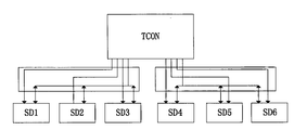
如图2所示,现有的液晶面板拓扑结构(panel topology)常采用一颗TCON IC搭配多颗Driver IC的架构进行连接;请同时参阅图3,TCON IC在第一阶段PhaseⅠ进行clock Training,第二阶段PhaseⅡ进行控制信号传送,第三阶段
PhaseⅢ开始传递正常显示的RGB数据;在PhaseⅠ若Driver IC接收到clock Training并能正常锁存clock时钟信号,则Driver IC的Lock pin(锁存引脚)处于高电平状态,由于上拉电阻的关系,TCON IC的Lock pin接收到高电平;若Driver IC不能接收到clock Training或即使正常接收到clock Training但并不能正常锁存clock时钟信号,则Driver IC将Lock拉低,TCON IC Lock pin接收到低电平,则TCON IC持续进行clock Training,无法进入下一个阶段。
液晶面板在设计验证阶段或批量生产过程中,若其中一颗Driver IC接收异常或Driver IC本身不良,则由于TCON IC持续clock Training整个液晶面板显示异常;液晶面板整体显示异常则无法快速确认TCON IC异常或Driver IC异常,即使确认Driver IC异常亦无法定位具体异常的Driver IC,因此,增加了设计调试的复杂程度,并且增加了批量生产异常分析所需的时间。
发明内容
为克服现有技术的不足,提供一种能够避免面板整体显示异常、加快设计验证速度且减少批量生产分析时间的液晶面板检测系统及方法。
本发明的目的是通过以下技术方案来实现的:一种液晶面板检测系统,包括时序控制芯片,所述时序控制芯片包括用于接收锁存信号的处理单元、与所述处理单元相连的侦测控制单元及与所述侦测控制单元相连的点对点传输单元,所述侦测控制单元实时侦测所述点对点传输单元的状态,并根据侦测结果发出控制信号至所述处理单元,所述处理单元根据接收到的控制信号使得所述时序控制芯片进行时序控制信号的传送,并开始传输正常显示的RGB数据,所述侦测控制单元输出的控制信号的优先级大于所述锁存信号的优先级。
所述侦测控制单元为计时器,当所述时序控制芯片进行时钟训练时,所述计时器开始计时。
当所述计时器判断时钟训练的时间大于预先设定的时间时,发出超出设定时间的控制信号至所述处理单元,当所述处理单元接收到所述计时器发出的超时信号时,强制使得所述时序控制芯片进行时序控制信号的传送,并开始传输
正常显示的RGB数据。
所述侦测控制单元为计数器,当所述时序控制芯片进行时钟训练时,所述计数器开始计数。
当所述计数器判断时钟训练的时间大于预先设定的周期时,发出超出设定周期的控制信号至所述处理单元,当所述处理单元接收到所述计数器发出的控制信号时,强制使得所述时序控制芯片进行时序控制信号的传送,并开始传输正常显示的RGB数据。
一种液晶面板检测方法,包括以下步骤:
时序控制芯片进行时钟训练;
判断是否所有的驱动芯片均能正常锁存时钟信号,如果是,则锁存信号处于高电平,进入下一步;
所述时序控制芯片进行时序控制信号的传送;
所述时序控制芯片开始传输正常显示的RGB数据。
如果判断不是所有的驱动芯片均能正常锁存时钟信号,则继续进行时钟训练,直至时钟训练的时间超过预先设定的时间或时钟训练的周期大于预先设定的周期时,所述时序控制芯片不再处理锁存信号,所述时序控制芯片进行时序控制信号的传送,并开始传输正常显示的RGB数据。
本发明的有益效果是:加快产品设计验证速度,加快产品上市时间,增加产品竞争力,提高批量生产异常分析速度,节约工时、产能,且降低成本。
图1为现有技术中point to point信号时序图;
图2为现有技术中的的面板拓扑结构;
图3为现有技术中液晶面板点对点传输结构的传输流程图;
图4为本发明液晶面板检测系统的系统结构图;
图5为本发明液晶面板检测系统一种实施方式的系统结构图;
图6为本发明液晶面板检测系统另一实施方式的系统结构图;
图7为本发明液晶面板检测方法的流程图。
下面,将结合附图对本发明各实施例作详细介绍。
请参阅图4,图4为本发明液晶面板检测系统的系统结构图。本发明液晶面板检测系统包括时序控制芯片,时序控制芯片包括用于接收锁存信号的处理单元、与处理单元相连的侦测控制单元及与侦测控制单元相连的点对点传输单元。
侦测控制单元实时侦测点对点传输单元的状态,并根据侦测结果发出控制信号至处理单元,处理单元根据接收到的控制信号使得时序控制芯片进行时序控制信号的传送,并开始传输正常显示的RGB数据。其中,侦测控制单元输出的控制信号的优先级大于锁存信号的优先级。
请参阅图5,图5为本发明液晶面板检测系统一种实施方式的系统结构图。其中,侦测控制单元可为计时器,持续侦测点对点传输单元的状态,当时序控制芯片进入第一阶段PhaseⅠ进行时钟训练时,计时器开始计时,当计时器判断时钟训练的时间大于预先设定的时间T时,计时器发出超出设定时间的控制信号至处理单元,当处理单元接收到计时器发出的超时信号时,强制使得时序控制芯片进入第二阶段PhaseⅡ与第三阶段PhaseⅢ,即进行时序控制信号的传送,并开始传输正常显示的RGB数据;此时,能够正常锁存时钟信号的驱动芯片,可以正常接收时序控制芯片发出的数据信号,除了不能正常锁存时钟信号的驱动芯片对应区域外的液晶面板显示正常。
请参阅图6,图6为本发明液晶面板检测系统另一种实施方式的系统结构图。其中,侦测控制单元可为计数器,持续侦测点对点传输单元的状态,当时序控制芯片进入第一阶段PhaseⅠ进行时钟训练时,计数器开始计数,当计数器判断时钟训练的时间大于预先设定的周期N时,计数器发出超出设定周期的
控制信号至处理单元,当处理单元接收到计数器发出的控制信号时,强制使得时序控制芯片进入第二阶段PhaseⅡ与第三阶段PhaseⅢ,即进行时序控制信号的传送,并开始传输正常显示的RGB数据;此时,能够正常锁存时钟信号的驱动芯片,可以正常接收时序控制芯片发出的数据信号,除了不能正常锁存时钟信号的驱动芯片对应区域外的液晶面板显示正常。
请参阅图7,图7为本发明液晶面板检测方法的流程图。本发明液晶面板检测方法包括以下步骤:
步骤一,时序控制芯片进入第一阶段PhaseⅠ进行时钟训练。
[根据细则26改正15.08.2016]
步骤二,判断是否所有的驱动芯片均能正常锁存时钟信号,如果是,则锁存信号LOCK处于高电平H,进入下一步;如果否,则转入步骤一,继续进行时钟训练,直至时钟训练的时间time超过预先设定的时间T或时钟训练的周期cycle大于预先设定的周期N时,时序控制芯片不再处理锁存信号LOCK,直接进入下一步。
步骤二,判断是否所有的驱动芯片均能正常锁存时钟信号,如果是,则锁存信号LOCK处于高电平H,进入下一步;如果否,则转入步骤一,继续进行时钟训练,直至时钟训练的时间time超过预先设定的时间T或时钟训练的周期cycle大于预先设定的周期N时,时序控制芯片不再处理锁存信号LOCK,直接进入下一步。
步骤三,时序控制芯片进入第二阶段PhaseⅡ,进行时序控制信号的传送。
步骤四,时序控制芯片进入第三阶段PhaseⅢ,开始传输正常显示的RGB数据。
本发明液晶面板检测系统及方法通过改变点对点传输结构的流程,避免了液晶面板整体显示异常的情况,加快了设计验证的速度且减少了批量生产分析时间,节约了工时和产能,降低了成本,增加了产品竞争力。
Claims (10)
- 一种液晶面板检测系统,其中,所述液晶面板检测系统包括时序控制芯片,所述时序控制芯片包括用于接收锁存信号的处理单元、与所述处理单元相连的侦测控制单元及与所述侦测控制单元相连的点对点传输单元,所述侦测控制单元实时侦测所述点对点传输单元的状态,并根据判断是否所有的驱动芯片均能正常锁存时钟信号及所述时序控制芯片进行时钟训练的时间与预先设定值进行比较后的侦测结果发出控制信号至所述处理单元,所述处理单元根据接收到的控制信号使得所述时序控制芯片进行时序控制信号的传送,并开始传输正常显示的RGB数据至液晶面板显示单元,所述侦测控制单元输出的控制信号的优先级大于所述锁存信号的优先级。
- 根据权利要求1所述的液晶面板检测系统,其中,所述侦测控制单元为计时器,当所述时序控制芯片进行时钟训练时,所述计时器开始计时。
- 根据权利要求2所述的液晶面板检测系统,其中,当所述计时器判断时钟训练的时间大于预先设定的时间时,发出超出设定时间的控制信号至所述处理单元,当所述处理单元接收到所述计时器发出的超时信号时,强制使得所述时序控制芯片进行时序控制信号的传送,并开始传输正常显示的RGB数据。
- 根据权利要求1所述的液晶面板检测系统,其中,所述侦测控制单元为计数器,当所述时序控制芯片进行时钟训练时,所述计数器开始计数。
- 根据权利要求4所述的液晶面板检测系统,其中,当所述计数器判断时钟训练的时间大于预先设定的周期时,发出超出设定周期的控制信号至所述处理单元,当所述处理单元接收到所述计数器发出的控制信号时,强制使得所述时序控制芯片进行时序控制信号的传送,并开始传输正常显示的RGB数据。
- 一种液晶面板检测方法,包括以下步骤:时序控制芯片进行时钟训练;时序控制芯片的侦测控制单元判断是否所有的驱动芯片均能正常锁存时钟信号,并根据所述时序控制芯片进行时钟训练的时间与预先设定值进行比较后的侦测结果发出控制信号至处理单元;所述时序控制芯片进行时序控制信号的传送;所述时序控制芯片开始传输正常显示的RGB数据。
- 根据权利要求6所述的液晶面板检测方法,其中,所述侦测控制单元为计时器,当所述时序控制芯片进行时钟训练时,所述计时器开始计时。
- 根据权利要求7所述的液晶面板检测方法,其中,当所述计时器判断时钟训练的时间大于预先设定的时间时,发出超出设定时间的控制信号至所述处理单元,当所述处理单元接收到所述计时器发出的超时信号时,强制使得所述时序控制芯片进行时序控制信号的传送,并开始传输正常显示的RGB数据。
- 根据权利要求6所述的液晶面板检测方法,其中,所述侦测控制单元为计数器,当所述时序控制芯片进行时钟训练时,所述计数器开始计数。
- 根据权利要求9所述的液晶面板检测方法,其中,当所述计数器判断时钟训练的时间大于预先设定的周期时,发出超出设定周期的控制信号至所述处理单元,当所述处理单元接收到所述计数器发出的控制信号时,强制使得所述时序控制芯片进行时序控制信号的传送,并开始传输正常显示的RGB数据。
Priority Applications (1)
| Application Number | Priority Date | Filing Date | Title |
|---|---|---|---|
| US15/103,886 US10168559B2 (en) | 2016-04-19 | 2016-05-24 | Liquid crystal display detecting system and a method thereof |
Applications Claiming Priority (2)
| Application Number | Priority Date | Filing Date | Title |
|---|---|---|---|
| CN201610244926.4 | 2016-04-19 | ||
| CN201610244926.4A CN105719587B (zh) | 2016-04-19 | 2016-04-19 | 液晶面板检测系统及方法 |
Publications (1)
| Publication Number | Publication Date |
|---|---|
| WO2017181474A1 true WO2017181474A1 (zh) | 2017-10-26 |
Family
ID=56161373
Family Applications (1)
| Application Number | Title | Priority Date | Filing Date |
|---|---|---|---|
| PCT/CN2016/083078 Ceased WO2017181474A1 (zh) | 2016-04-19 | 2016-05-24 | 液晶面板检测系统及方法 |
Country Status (3)
| Country | Link |
|---|---|
| US (1) | US10168559B2 (zh) |
| CN (1) | CN105719587B (zh) |
| WO (1) | WO2017181474A1 (zh) |
Families Citing this family (6)
| Publication number | Priority date | Publication date | Assignee | Title |
|---|---|---|---|---|
| CN108694917B (zh) * | 2017-06-09 | 2021-10-22 | 京东方科技集团股份有限公司 | 数据传输方法、组件及显示装置 |
| KR102514636B1 (ko) * | 2018-10-22 | 2023-03-28 | 주식회사 엘엑스세미콘 | 디스플레이장치를 구동하기 위한 데이터처리장치, 데이터구동장치 및 시스템 |
| CN110310586B (zh) * | 2019-05-31 | 2022-12-20 | 晶晨半导体(上海)股份有限公司 | 一种tconless板的硬件调试方法 |
| CN111326098B (zh) * | 2020-04-08 | 2022-10-04 | Tcl华星光电技术有限公司 | 源极驱动控制方法、装置及显示终端 |
| CN112415367B (zh) * | 2020-11-25 | 2023-08-25 | 北京奕斯伟计算技术股份有限公司 | 驱动芯片异常侦测方法、装置、电子设备及可读存储介质 |
| CN115188310B (zh) * | 2022-07-08 | 2024-09-24 | 昆山龙腾光电股份有限公司 | 源级驱动芯片及其控制方法 |
Citations (5)
| Publication number | Priority date | Publication date | Assignee | Title |
|---|---|---|---|---|
| US20110037758A1 (en) * | 2009-08-13 | 2011-02-17 | Jung-Pil Lim | Clock and data recovery circuit of a source driver and a display device |
| CN102214429A (zh) * | 2010-04-05 | 2011-10-12 | 硅工厂股份有限公司 | 使用具有嵌入式时钟信号的单一位准数据传输的显示器驱动系统 |
| CN103794184A (zh) * | 2012-10-31 | 2014-05-14 | 乐金显示有限公司 | 显示装置及其驱动方法 |
| CN103903577A (zh) * | 2012-12-27 | 2014-07-02 | 天钰科技股份有限公司 | 显示装置及其驱动方法、时序控制电路的数据处理及输出方法 |
| CN103928004A (zh) * | 2013-01-10 | 2014-07-16 | 三星电子株式会社 | 显示驱动电路和在显示驱动电路中的传输数据的方法 |
Family Cites Families (12)
| Publication number | Priority date | Publication date | Assignee | Title |
|---|---|---|---|---|
| JP2008015006A (ja) * | 2006-07-03 | 2008-01-24 | Nec Electronics Corp | 表示コントローラ、表示装置、及び表示データ転送方法 |
| KR101508719B1 (ko) * | 2008-10-06 | 2015-04-03 | 삼성디스플레이 주식회사 | 구동유닛 및 이를 갖는 표시장치 |
| KR101310919B1 (ko) * | 2008-12-15 | 2013-09-25 | 엘지디스플레이 주식회사 | 액정표시장치 |
| KR101325362B1 (ko) * | 2008-12-23 | 2013-11-08 | 엘지디스플레이 주식회사 | 액정표시장치 |
| KR101654218B1 (ko) * | 2010-01-13 | 2016-09-06 | 삼성전자주식회사 | 스프레드 스펙트럼 클럭 발생기 |
| US8390614B2 (en) * | 2010-03-08 | 2013-03-05 | Himax Technologies Limited | Timing controller and clock signal detection circuit thereof |
| US8564522B2 (en) * | 2010-03-31 | 2013-10-22 | Apple Inc. | Reduced-power communications within an electronic display |
| KR101872430B1 (ko) * | 2011-08-25 | 2018-07-31 | 엘지디스플레이 주식회사 | 액정표시장치 및 그 구동 방법 |
| TWI469115B (zh) * | 2012-08-31 | 2015-01-11 | Raydium Semiconductor Corp | 時序控制器、顯示裝置及其驅動方法 |
| KR102011953B1 (ko) * | 2012-11-28 | 2019-08-19 | 엘지디스플레이 주식회사 | 데이터 비트 뎁쓰 검출 방법과 이를 이용한 표시장치의 인터페이스 장치 |
| CN103389455B (zh) * | 2013-08-09 | 2015-11-11 | 友达光电(苏州)有限公司 | 驱动芯片的检测系统及检测方法 |
| KR20150139105A (ko) * | 2014-06-02 | 2015-12-11 | 삼성디스플레이 주식회사 | 광원 구동 방법, 이 방법을 수행하는 광원 구동 장치 및 이 광원 구동 장치를 포함하는 표시 장치 |
-
2016
- 2016-04-19 CN CN201610244926.4A patent/CN105719587B/zh not_active Expired - Fee Related
- 2016-05-24 US US15/103,886 patent/US10168559B2/en active Active
- 2016-05-24 WO PCT/CN2016/083078 patent/WO2017181474A1/zh not_active Ceased
Patent Citations (5)
| Publication number | Priority date | Publication date | Assignee | Title |
|---|---|---|---|---|
| US20110037758A1 (en) * | 2009-08-13 | 2011-02-17 | Jung-Pil Lim | Clock and data recovery circuit of a source driver and a display device |
| CN102214429A (zh) * | 2010-04-05 | 2011-10-12 | 硅工厂股份有限公司 | 使用具有嵌入式时钟信号的单一位准数据传输的显示器驱动系统 |
| CN103794184A (zh) * | 2012-10-31 | 2014-05-14 | 乐金显示有限公司 | 显示装置及其驱动方法 |
| CN103903577A (zh) * | 2012-12-27 | 2014-07-02 | 天钰科技股份有限公司 | 显示装置及其驱动方法、时序控制电路的数据处理及输出方法 |
| CN103928004A (zh) * | 2013-01-10 | 2014-07-16 | 三星电子株式会社 | 显示驱动电路和在显示驱动电路中的传输数据的方法 |
Also Published As
| Publication number | Publication date |
|---|---|
| CN105719587B (zh) | 2019-03-12 |
| US10168559B2 (en) | 2019-01-01 |
| CN105719587A (zh) | 2016-06-29 |
| US20180101034A1 (en) | 2018-04-12 |
Similar Documents
| Publication | Publication Date | Title |
|---|---|---|
| WO2017181474A1 (zh) | 液晶面板检测系统及方法 | |
| TWI428896B (zh) | 資料驅動器用之具有監測單元的顯示器驅動系統 | |
| US11211023B2 (en) | Display method of display device and display device | |
| US9778971B2 (en) | Slave device, master device, and communication method | |
| US10074339B2 (en) | Receiver circuit and operating method of the same | |
| TWI439846B (zh) | 用以控制電子裝置之操作狀態的方法與裝置 | |
| US9852673B2 (en) | Noise removal circuit | |
| WO2018036097A1 (zh) | 一种降低电磁干扰的驱动方法及驱动装置 | |
| TWI507000B (zh) | 使用資料流之資料傳輸(tx)及接收(rx)系統的介面方法 | |
| US20210103547A1 (en) | Mipi d-phy receiver auto rate detection and high-speed settle time control | |
| CN103970628B (zh) | 自动化检测系统及其自动化检测方法 | |
| TW201428480A (zh) | 在通訊埠中減少閒置功率之技術 | |
| US20160118010A1 (en) | Display Driving Apparatus, Source Driver and Skew Adjustment Method | |
| US20100060557A1 (en) | Data de-skew block device and method of de-skewing transmitted data | |
| US20200159280A1 (en) | Reception apparatus with clock failure recovery and transmission system including the same | |
| CN110310586B (zh) | 一种tconless板的硬件调试方法 | |
| CN106289729A (zh) | 一种太赫兹或红外焦平面探测器自动测试系统和方法 | |
| WO2019033825A1 (zh) | 驱动电路及其控制方法、显示面板和显示装置 | |
| CN102591046B (zh) | 液晶屏的rgb接口测试方法 | |
| CN102034409B (zh) | 用于传输数据的方法和应用此方法的显示器 | |
| CN204256325U (zh) | 实现两种模式的mipi模组测试系统 | |
| TWI420490B (zh) | 於顯示器之時序控制器和源極驅動器間傳輸資料之方法與應用此資料傳輸方法之顯示器 | |
| TW201729581A (zh) | 時序控制晶片無畫面檢測系統及其方法 | |
| JP2002033754A (ja) | シリアルデータ転送装置、その制御方法、及び、通信装置 | |
| US20170185216A1 (en) | Synchronization Method and Touch Signal Processing System Using the Same |
Legal Events
| Date | Code | Title | Description |
|---|---|---|---|
| WWE | Wipo information: entry into national phase |
Ref document number: 15103886 Country of ref document: US |
|
| NENP | Non-entry into the national phase |
Ref country code: DE |
|
| 121 | Ep: the epo has been informed by wipo that ep was designated in this application |
Ref document number: 16899061 Country of ref document: EP Kind code of ref document: A1 |
|
| 122 | Ep: pct application non-entry in european phase |
Ref document number: 16899061 Country of ref document: EP Kind code of ref document: A1 |