WO2017169775A1 - 画像センサ - Google Patents
画像センサ Download PDFInfo
- Publication number
- WO2017169775A1 WO2017169775A1 PCT/JP2017/010370 JP2017010370W WO2017169775A1 WO 2017169775 A1 WO2017169775 A1 WO 2017169775A1 JP 2017010370 W JP2017010370 W JP 2017010370W WO 2017169775 A1 WO2017169775 A1 WO 2017169775A1
- Authority
- WO
- WIPO (PCT)
- Prior art keywords
- current
- transistor
- photodiode
- mirror circuit
- primary side
- Prior art date
- Legal status (The legal status is an assumption and is not a legal conclusion. Google has not performed a legal analysis and makes no representation as to the accuracy of the status listed.)
- Ceased
Links
Images



Classifications
-
- H—ELECTRICITY
- H04—ELECTRIC COMMUNICATION TECHNIQUE
- H04N—PICTORIAL COMMUNICATION, e.g. TELEVISION
- H04N25/00—Circuitry of solid-state image sensors [SSIS]; Control thereof
- H04N25/70—SSIS architectures; Circuits associated therewith
-
- H—ELECTRICITY
- H04—ELECTRIC COMMUNICATION TECHNIQUE
- H04N—PICTORIAL COMMUNICATION, e.g. TELEVISION
- H04N25/00—Circuitry of solid-state image sensors [SSIS]; Control thereof
- H04N25/60—Noise processing, e.g. detecting, correcting, reducing or removing noise
- H04N25/62—Detection or reduction of noise due to excess charges produced by the exposure, e.g. smear, blooming, ghost image, crosstalk or leakage between pixels
-
- H—ELECTRICITY
- H04—ELECTRIC COMMUNICATION TECHNIQUE
- H04N—PICTORIAL COMMUNICATION, e.g. TELEVISION
- H04N25/00—Circuitry of solid-state image sensors [SSIS]; Control thereof
- H04N25/70—SSIS architectures; Circuits associated therewith
- H04N25/76—Addressed sensors, e.g. MOS or CMOS sensors
-
- H—ELECTRICITY
- H10—SEMICONDUCTOR DEVICES; ELECTRIC SOLID-STATE DEVICES NOT OTHERWISE PROVIDED FOR
- H10F—INORGANIC SEMICONDUCTOR DEVICES SENSITIVE TO INFRARED RADIATION, LIGHT, ELECTROMAGNETIC RADIATION OF SHORTER WAVELENGTH OR CORPUSCULAR RADIATION
- H10F39/00—Integrated devices, or assemblies of multiple devices, comprising at least one element covered by group H10F30/00, e.g. radiation detectors comprising photodiode arrays
- H10F39/10—Integrated devices
- H10F39/12—Image sensors
Definitions
- the present invention relates to an image sensor that detects an image by photocharge.
- CMOS Sensors for 3D Imaging p.42 Aizawa Kiyoharu, Hamamoto Takayuki, “Image Information Media Core Technology Series 9 CMOS Image Sensor”, Corona, August 2012, p.177
- Non-Patent Document 1 operates a MOS transistor connected to a photodiode as a switch, removes all the photoelectric charges accumulated in the photodiode, and resets the photodiode. is there.
- this configuration does not remove only the photocharge of noise components such as high background light, for example, there is a problem that the necessary photocharge cannot be left.
- the image sensor described in Non-Patent Document 2 operates a MOS transistor connected to a photodiode in a subthreshold region to remove only excess photocharge.
- this configuration tends to be affected by the process in producing the element and tends to cause manufacturing variations.
- the image sensor described in Non-Patent Document 2 has a problem that it is easily affected by various effects such as fluctuations in power supply voltage and temperature fluctuations.
- the present invention has been made in view of the above-described problems, and an object of the present invention is to provide an image sensor capable of suppressing noise and removing noise.
- an image sensor includes a photodiode and a transistor connected to the photodiode and configured to reduce photocharge accumulated in the photodiode, and the transistor is predetermined. It is a constant current transistor that flows a current of a predetermined value.
- a constant current transistor is connected to the photodiode. Therefore, by appropriately setting the magnitude of the current flowing through the constant current transistor, for example, photocharges of noise components such as background light are removed from the photodiode. be able to. Further, since the constant current transistor operates to pass a predetermined current, the current value is stabilized. For this reason, compared with the case where a transistor operated in, for example, a subthreshold region is used, it is less susceptible to various effects such as variations in process, power supply voltage, temperature, etc., and noise removal characteristics can be stabilized.
- the constant current transistor is a secondary transistor of a current mirror circuit that supplies a current having a predetermined ratio to the current flowing through the primary transistor.
- a constant ratio of current to the current flowing through the primary transistor of the current mirror circuit can be passed through the constant current transistor.
- the magnitude of the current flowing through the constant current transistor can be set according to the magnitude of the current flowing through the primary side transistor of the current mirror circuit. For this reason, for example, the magnitude of the current flowing through the constant current transistor can be adjusted even after the device is manufactured.
- the current mirror circuit can increase or decrease the current flowing through the primary side transistor.
- the magnitude of the current flowing through the constant current transistor that is the secondary side transistor can be adjusted according to the magnitude of the current flowing through the primary side transistor.
- a plurality of other secondary-side transistors connected to the primary-side transistor of the current mirror circuit are provided, and the other secondary-side transistor is predetermined with respect to the current flowing through the other primary-side transistor.
- a current mirror circuit configured to flow a current of a predetermined ratio, wherein the other current mirror circuit is configured to flow a current to a primary side transistor of the current mirror circuit among a plurality of other secondary side transistors. Can be selected.
- the sum of currents flowing through the plurality of other secondary transistors can be increased or decreased by individually switching between ON and OFF for the plurality of other secondary transistors.
- the magnitude of the current flowing through the primary transistor of the current mirror circuit can be adjusted according to the sum of the currents flowing through the plurality of other secondary transistors.
- the other current mirror circuit is configured to select the other secondary side transistor that causes a current to flow to the primary side transistor of the current mirror circuit in accordance with an exposure amount of light input to the photodiode. Yes.
- the current flowing through the primary side transistor of the current mirror circuit can be increased or decreased.
- the current flowing through the primary side transistor of the current mirror circuit can be reduced. The magnitude can be adjusted as a digital quantity. For this reason, the current flowing through the primary side transistor of the current mirror circuit can be digitally controlled.
- FIG. 1 is a circuit diagram showing an image sensor according to a first embodiment of the present invention.
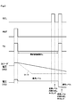
- 2 is a timing chart illustrating an example of a cathode voltage and the like of the photodiode in FIG. 1.
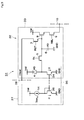
- It is a circuit diagram which shows the image sensor by the 2nd Embodiment of this invention.
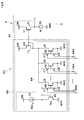
- It is a circuit diagram which shows the image sensor by the 3rd Embodiment of this invention.
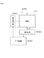
- It is a block diagram which shows the image imaging system by the 4th and 5th embodiment of this invention.
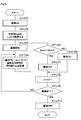
- It is a flowchart which shows the voltage setting process by the 4th Embodiment of this invention.
- It is a flowchart which shows the voltage setting process by the 5th Embodiment of this invention.
- It is a circuit diagram which shows the image sensor by a comparative example.
- 9 is a timing chart showing an example of a cathode voltage and the like of the photodiode in FIG.
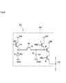
- FIG. 1 shows an image sensor 1 according to a first embodiment of the present invention.
- the image sensor 1 includes a pixel unit 2 including a plurality of pixel circuits 3 (only one is shown) and a current source circuit 15.
- the image sensor 1 captures an image input to the pixel unit 2, converts it into an electrical signal, and outputs it.
- the pixel circuit 3 includes a photodiode 4 (PD), a transfer transistor 5, a floating diffusion capacitor 6 (FD), a reset transistor 7, an amplification transistor 8, a selection transistor 9, and a constant current transistor 11. Yes.
- the pixel circuit 3 is formed on a semiconductor substrate.
- the transfer transistor 5, the reset transistor 7, the amplification transistor 8, and the selection transistor 9 are all constituted by NMOS transistors.
- a transfer transistor control signal TX is applied to the gate of the transfer transistor 5.
- a reset transistor control signal RST is applied to the gate of the reset transistor 7.
- a selection transistor control signal SEL is applied to the gate of the selection transistor 9.
- the photodiode 4 accumulates photocharges (electrons) corresponding to the intensity and amount of incident light.
- a ground voltage GND is applied to the anode of the photodiode 4.
- the cathode of the photodiode 4 is connected to the source of the transfer transistor 5.
- the drain of the transfer transistor 5 is connected to the source of the reset transistor 7 and to the gate of the amplification transistor 8.
- a power supply voltage Vdd is applied to the drain of the reset transistor 7.
- a power supply voltage Vdd is applied to the drain of the amplification transistor 8.
- the source of the selection transistor 9 is connected to the vertical signal line 10.
- the drain of the selection transistor 9 is connected to the source of the amplification transistor 8.
- the floating diffusion capacitor 6 is generally composed mainly of a wiring parasitic capacitance, but can be regarded as a configuration in which the ground voltage GND is applied to the other terminal.
- the floating diffusion capacitor 6 is an equivalent capacitance of a floating diffusion (floating region) that accumulates photoelectric charges as signal charges and converts the photoelectric charges into voltage.
- the constant current transistor 11 is composed of a PMOS transistor.
- the constant current transistor 11 constitutes a secondary side transistor that becomes a return destination of the current mirror circuit 12.
- the current mirror circuit 12 includes a constant current transistor 11, a primary side transistor 13, and a constant current source 14.
- the current mirror circuit 12 causes the constant current transistor 11 to pass a current I2 having a predetermined ratio with respect to the current I1 that flows through the primary transistor 13 that is the return source.
- the current mirror circuit 12 passes a current I 2 having the same magnitude as the current I 1 of the primary side transistor 13 to the constant current transistor 11.
- the present invention is not limited to this, and the primary side transistor 13 and the constant current transistor 11 may have different sizes.
- the drain of the constant current transistor 11 is connected to the cathode of the photodiode 4.
- a power supply voltage Vdd is applied to the source of the constant current transistor 11.
- the constant current transistor 11 is connected to the side (cathode side) of the photodiode 4 that accumulates photocharges (electrons).
- the primary side transistor 13 is composed of a PMOS transistor, like the constant current transistor 11.
- the drain of the primary side transistor 13 is connected to the constant current source 14. For this reason, the current Ibias from the constant current source 14 flows through the primary side transistor 13.
- a power supply voltage Vdd is applied to the source of the primary side transistor 13.
- the gate of the primary side transistor 13 is connected to the drain of the primary side transistor 13 and also to the gate of the constant current transistor 11 serving as the secondary side transistor.
- Current I2 flows.
- a portion of the current mirror circuit 12 in which the constant current transistor 11 is omitted constitutes a current source circuit 15 that sets the magnitude of the current I 2 flowing through the constant current transistor 11.
- FIG. 1 shows a configuration in which one photodiode 4 is connected to one amplification transistor 8 in order to simplify the configuration.
- a plurality of sets of photodiodes 4 and transfer transistors 5 are connected in parallel to one amplification transistor 8 in order to increase the area efficiency of the pixel unit 2. Even in this case, the same effect as the configuration shown in FIG. 1 can be obtained by connecting one constant current transistor 11 to one photodiode 4 in each group.
- the image sensor 1 according to the first embodiment of the present invention has the above-described configuration. Next, the operation of the pixel circuit 3 will be described with reference to FIG. 1 and FIG.
- the reset transistor 7 is set to a conductive state (ON) by a reset transistor control signal RST.
- the transfer transistor 5 is also set to a conductive state by the transfer transistor control signal TX.
- both the photodiode 4 and the floating diffusion capacitor 6 are reset.
- the transfer transistor 5 and the reset transistor 7 are switched to a cut-off state (OFF).
- the photodiode 4 of the pixel circuit 3 generates a photocharge corresponding to the incident light. For this reason, the cathode voltage of the photodiode 4 decreases according to the photocharge.
- the current I 2 having the same magnitude as the current I 1 of the primary transistor 13 of the current mirror circuit 12 flows through the constant current transistor 11. Therefore, a part of the photoelectric charge generated in the photodiode 4 is removed according to the current I2.
- the slope when the cathode voltage drops becomes gentle according to the magnitude of the current I2.
- the voltage of the reference level of the floating diffusion capacitor 6 is read before a predetermined charge accumulation period Tc elapses after the reset operation is completed.
- the selection transistor 9 is temporarily set to a conductive state (ON) by the selection transistor control signal SEL.
- the voltage of the floating diffusion capacitor 6 is output to the vertical signal line 10 before the photocharge of the photodiode 4 is transferred.
- the selection transistor 9 is switched to the cutoff state (OFF).
- the transfer transistor 5 is set to a conductive state (ON) by the transfer transistor control signal TX.
- the selection transistor 9 is also set to a conductive state (ON) by the selection transistor control signal SEL.
- the photoelectric charge accumulated in the photodiode 4 is transferred to the floating diffusion via the transfer transistor 5 set to the conductive state, and the floating diffusion capacitor 6 is charged.
- the amplification transistor 8 amplifies the voltage of the floating diffusion capacitor 6 and outputs it to the vertical signal line 10 via the selection transistor 9.
- the image sensor 1 removes the photocharge of the background light by causing the current I2 to flow through the constant current transistor 11. Such an excess photocharge removal effect will be specifically described below.
- the image sensor 21 according to this comparative example includes a pixel circuit 22 similar to the pixel circuit 3 according to the first embodiment. Therefore, the pixel circuit 22 includes the photodiode 4, the transfer transistor 5, the floating diffusion capacitor 6, the reset transistor 7, the amplification transistor 8, and the selection transistor 9.
- the cathode of the photodiode 4 is connected to the source of the NMOS transistor 23.
- the power supply voltage Vdd is supplied to the drain of the NMOS transistor 23.
- the image sensor 21 of the comparative example is different from the image sensor 1 according to the first embodiment.
- FIG. 9 shows an example of a timing chart when the image sensor 21 according to the comparative example is operated.
- This timing chart assumes that light is always incident without assuming a mechanical shutter like a digital camera, for example. Therefore, photocharge is always generated in the photodiode 4. Further, assuming that the incident light intensity is constant, a constant amount of photocharge is generated per unit time in the photodiode 4 during the charge accumulation period Tc, and the cathode voltage of the photodiode 4 drops with a constant slope.
- the NMOS transistor 23 is operated (weak inversion operation) in the subthreshold region equal to or lower than the threshold value.
- a current Ist flows through the photodiode 4, and the slope of the change in the cathode voltage of the photodiode 4 becomes gentle as shown by the solid line in FIG. 9. For this reason, sticking to the lower limit voltage at the signal level read timing can be avoided.
- the NMOS transistor 23 when the NMOS transistor 23 is weakly inverted, it is easily affected by process variations, power supply variations, gate voltage variations, and temperature variations, and the current Ist tends to be unstable. As a result, as shown by a broken line in FIG. 9, the slope of the cathode voltage of the photodiode 4 varies from pixel to pixel and even in the same pixel with time.
- FIG. 2 shows an example of a timing chart when the image sensor 1 according to the first embodiment is operated.
- the incident light intensity is constant.
- a constant photocharge is generated per unit time in the photodiode 4 during the charge accumulation period Tc, and the cathode voltage of the photodiode 4 drops with a constant slope.
- the constant current transistor 11 that is the secondary transistor of the current mirror circuit 12 is connected to the photodiode 4.
- a constant current I2 is supplied via the constant current transistor 11, the photocharge accumulated in the photodiode 4 is discharged to the power supply voltage Vdd side (power supply).
- the constant current transistor 11 constitutes the current mirror circuit 12
- a predetermined current I2 can be stably supplied to the photodiode 4.
- the constant current transistor 11 is operated in the saturation region. For this reason, it is hard to be influenced by a process, and the characteristic variation for every element can be suppressed. In addition, the signal level can be stabilized without being affected by fluctuations in the power supply voltage Vdd and temperature changes. As a result, in the first embodiment, it is possible to suppress variations among pixels and changes with time in the same pixel.
- the constant current transistor 11 since the constant current transistor 11 is connected to the photodiode 4, by setting the magnitude of the current I2 flowing through the constant current transistor 11 appropriately, for example, noise such as background light. The component photocharge can be removed from the photodiode 4. Further, since the constant current transistor 11 operates so as to flow a predetermined current I2, the magnitude (current value) of the current I2 is stabilized. For this reason, it is difficult to be affected by various effects such as variations in process, power supply voltage, temperature, etc., and noise removal characteristics can be stabilized.
- the constant current transistor 11 is a secondary side transistor of the current mirror circuit 12
- a current I 2 having the same magnitude as the current I 1 flowing through the primary side transistor 13 of the current mirror circuit 12 can be supplied to the constant current transistor 11.
- the magnitude of the current I2 flowing through the constant current transistor 11 can be set according to the magnitude of the current I1 flowing through the primary side transistor 13 of the current mirror circuit 12. For this reason, for example, the magnitude of the current flowing through the constant current transistor 11 can be adjusted even after the device is manufactured.
- the image sensor 1 tends to have a large pixel size.
- the image sensor 1 for distance measurement has a low pixel number, and therefore the demand for pixel size reduction is low. High background light measures are required. For this reason, when the present invention is applied to the image sensor 1 for distance measurement, the effect is great.
- FIG. 3 shows a second embodiment of the present invention.
- a feature of the second embodiment is that a current mirror circuit is configured using NMOS transistors.
- the same components as those in the first embodiment described above are denoted by the same reference numerals, and description thereof is omitted.
- the image sensor 31 according to the second embodiment includes a pixel unit 32 including a plurality of pixel circuits 33 (only one is shown) and a current source circuit 37. I have.
- the pixel circuit 33 is configured in substantially the same manner as the pixel circuit 3 according to the first embodiment. Therefore, the pixel circuit 33 includes a photodiode 4, a transfer transistor 5, a floating diffusion capacitor 6, a reset transistor 7, an amplification transistor 8, a selection transistor 9, and a constant current transistor 34.
- the power supply voltage Vdd is applied to the cathode of the photodiode 4.
- the anode of the photodiode 4 is connected to the source of the transfer transistor 5.
- the photodiode 4 accumulates photocharges (holes) corresponding to the intensity and amount of incident light.
- a reset voltage Vreset (Vreset> GND + Vth) larger than a value obtained by adding the ground voltage GND and the threshold voltage Vth of the NMOS transistor is applied to the drain of the reset transistor 7.
- the constant current transistor 34 is composed of an NMOS transistor, like the other transistors 5, 7, 8, 9.
- the constant current transistor 34 constitutes a secondary side transistor that is a return destination of the current mirror circuit 35.
- the current mirror circuit 35 includes a constant current transistor 34, a primary side transistor 36, and a constant current source 14.
- the current mirror circuit 35 causes the constant current transistor 34 to pass a current I2 having a predetermined ratio with respect to the current I1 that flows through the primary side transistor 36 that is the return source.
- the ratio of the current I1 flowing through the primary transistor 36 and the current I2 flowing through the constant current transistor 34 is determined by the ratio between the size of the primary transistor 36 and the size of the constant current transistor 34.
- the description will be made on the assumption that the size of the primary side transistor 36 and the size of the constant current transistor 34 are the same, that is, the case where the current I1 and the current I2 have the same size.
- the present invention is not limited to this, and the primary side transistor 36 and the constant current transistor 34 may have different sizes.
- the drain of the constant current transistor 34 is connected to the anode of the photodiode 4.
- a ground voltage GND is applied to the source of the constant current transistor 34.
- the constant current transistor 34 is connected to the side (anode side) of the photodiode 4 that accumulates photocharges (holes).
- the primary side transistor 36 is configured by an NMOS transistor.
- a power supply voltage Vdd is applied to the drain of the primary side transistor 36 via the constant current source 14.
- a ground voltage GND is applied to the source of the primary side transistor 36.
- the gate of the primary side transistor 36 is connected to the drain of the primary side transistor 36 and is also connected to the gate of the constant current transistor 34 serving as a secondary side transistor.
- the pixel circuit 33 can be configured with only the NMOS transistor without adding the PMOS transistor, so that no additional mask is required in the manufacturing process. An increase in manufacturing cost can be suppressed.
- the reset voltage Vreset needs to be stably supplied separately from the power supply voltage Vdd and the ground voltage GND. That is, when resetting the photocharge accumulated in the photodiode 4, in the first embodiment, the photocharge (electrons) is discharged to the power supply voltage Vdd side, so that the source voltage of the amplification transistor 8 is the power supply voltage. It rises closer to Vdd. On the other hand, in the second embodiment, photocharges (holes) are released toward the ground, so that the source voltage of the amplification transistor 8 drops toward the ground voltage GND at the time of reset.
- the amplification transistor 8 is turned off, and a voltage corresponding to the reset voltage Vreset cannot be output to the source of the amplification transistor 8. Therefore, it is necessary to set the reset voltage Vreset supplied to the drain of the reset transistor 7 higher than the ground voltage GND by a threshold voltage Vth or higher, and a separate reset voltage line 38 is necessary.
- FIG. 4 shows a third embodiment of the present invention.
- the current mirror circuit can variably set the current flowing through the primary side transistor. Note that in the third embodiment, the same components as those in the first embodiment described above are denoted by the same reference numerals, and description thereof is omitted.
- the image sensor 41 according to the third embodiment includes a pixel unit 2 including a plurality of pixel circuits 3 (only one is shown) and a current source circuit 49. I have.
- the constant current transistor 11 constitutes a secondary side transistor that becomes a return destination of the current mirror circuit 42.
- the current mirror circuit 42 includes a constant current transistor 11, a primary side transistor 43, and a variable current source circuit 44 including a constant current source 14.
- the current mirror circuit 42 causes the constant current transistor 11 to pass a current I2 having a predetermined ratio with respect to the current I1 that flows through the primary transistor 43 that is the return source.
- the ratio of the current I 1 flowing through the primary transistor 43 and the current I 2 flowing through the constant current transistor 11 is determined by the ratio between the size of the primary transistor 43 and the size of the constant current transistor 11.
- the description will be made on the assumption that the size of the primary side transistor 43 and the size of the constant current transistor 11 are the same, that is, the case where the current I1 and the current I2 are the same.
- the present invention is not limited to this, and the primary side transistor 43 and the constant current transistor 11 may have different sizes.
- the primary side transistor 43 is composed of a PMOS transistor, like the constant current transistor 11.
- the drain of the primary side transistor 43 is connected to the drains of a plurality (for example, m) of current setting secondary side transistors 46 constituting the variable current source circuit 44.
- a power supply voltage Vdd is applied to the source of the primary side transistor 43.
- the gate of the primary side transistor 43 is connected to the drain of the primary side transistor 43 and is connected to the gate of the constant current transistor 11 serving as the secondary side transistor.
- the variable current source circuit 44 constitutes another current mirror circuit.
- the variable current source circuit 44 includes a constant current source 14, a current setting primary side transistor 45 (another primary side transistor), and a plurality of current setting secondary side transistors 46 (another secondary side transistor). Contains.
- the variable current source circuit 44 causes a current Ib having a predetermined ratio to the current Ia flowing through the current setting primary side transistor 45 to be the return source to flow to the current setting secondary transistor 46 to be the return destination.
- the ratio between the current Ia flowing through the current setting primary transistor 45 and the current Ib flowing through the current setting secondary transistor 46 is determined by the size of the current setting primary transistor 45 and the current setting secondary transistor 46. Depends on the ratio of size. In the following, in order to simplify the explanation, it is assumed that the current setting primary side transistor 45 and the current setting secondary transistor 46 have the same size, that is, the current Ia and the current Ib have the same size. Explained.
- the present invention is not limited to this, and the current setting primary side transistor 45 and the current setting secondary side transistor 46 may be of different sizes.
- the plurality of current setting secondary transistors 46 may also have different sizes.
- the ratio of the sizes of the plurality of current setting secondary transistors 46 may correspond to, for example, a binary code or a thermometer code, or may correspond to another code.
- the plurality of current setting secondary transistors 46 are formed in different sizes, the currents Ib flowing through the plurality of current setting secondary transistors 46 can be made different from each other. For this reason, the degree of freedom when adjusting the magnitude of the current I1 flowing through the primary side transistor 43 can be increased.
- the current setting primary side transistor 45 and the current setting secondary side transistor 46 are both constituted by NMOS transistors.
- the power supply voltage Vdd is applied to the drain of the current setting primary side transistor 45 via the constant current source 14.
- the ground voltage GND is applied to the source of the current setting primary side transistor 45.
- the gate of the current setting primary side transistor 45 is connected to the drain of the current setting primary side transistor 45 and is also connected to the gate of the current setting secondary side transistor 46 via the first switch 47.
- the drain of the current setting secondary side transistor 46 is connected to the drain of the primary side transistor 43.
- the ground voltage GND is applied to the source of the current setting secondary transistor 46.
- the gate of the current setting secondary transistor 46 is connected to the gate of the current setting secondary transistor 46 through the first switch 47 and is connected to the ground through the second switch 48. .
- a control signal is directly input to the first switch 47 from a data processing unit (not shown).
- a control signal is input to the second switch 48 from the data processing unit via the NOT circuit 48A.
- a control signal is input to the first and second switches 47 and 48 from the data processing unit so that the switching states are opposite to each other.
- the other is operated so that the other is disconnected (OFF).
- the one whose gate is connected to the gate of the current setting primary side transistor 45 is the current between the drain and the source of the current setting primary side transistor 45.
- Copy Ia (Ia Ibias). That is, a current Ib having the same magnitude as the current Ia flows between the drain and source of the current setting secondary transistor 46.
- a portion of the current mirror circuit 42 from which the constant current transistor 11 is omitted constitutes a current source circuit 49 that sets the magnitude of the current I 2 flowing through the constant current transistor 11.
- the third embodiment further includes another current mirror circuit (variable current source circuit 44) having a plurality of current setting secondary transistors 46 connected to the primary transistor 43 of the current mirror circuit 42.
- the variable current source circuit 44 is configured to be able to select one of the plurality of current setting secondary transistors 46 that allows current to flow to the primary transistor 43 of the current mirror circuit 42. Therefore, the magnitude of the current flowing through the primary side transistor 43 of the current mirror circuit 42 can be adjusted by switching the operating state of the plurality of current setting secondary side transistors 46.
- the currents Ib flowing through the plurality of current setting secondary transistors 46 have the same magnitude. However, the currents Ib flowing through the plurality of current setting secondary transistors 46 are reduced. The sizes may be different from each other. In this case, not only the number of current setting secondary transistors 46 that are turned on, but also the current that flows through the primary transistor 43 of the current mirror circuit 42 by switching the current setting secondary transistors 46 that are turned on. I1 can be adjusted. Therefore, for example, when the ratio of the current Ib flowing through the plurality of current setting secondary transistors 46 is set in accordance with the binary code or the like, the current I1 flowing through the primary transistor 43 of the current mirror circuit 42 is digitally controlled. be able to.
- the pixel portion 2 (pixel circuit 3) according to the first embodiment is exemplified.
- the third embodiment is applied to the pixel portion 32 (pixel circuit 33) according to the second embodiment. You may apply.
- FIG. 5 and FIG. 6 show a fourth embodiment of the present invention.
- the feature of the fourth embodiment is that an image photographing system is configured using the image sensor according to the first embodiment. Note that in the fourth embodiment, the same components as those in the first embodiment described above are denoted by the same reference numerals, and description thereof is omitted.
- the image photographing system 51 includes the image sensor 1 according to the first embodiment, a reading unit 52, and a data processing unit 53.
- the image sensor 1, the reading unit 52, and the data processing unit 53 of the image capturing system 51 tend to have the same semiconductor substrate.
- the semiconductor substrates of the image sensor 1, the reading unit 52, and the data processing unit 53 may be the same or different from each other.
- the reading unit 52 includes a programmable gain amplifier and an A / D conversion circuit.
- the reading unit 52 converts an analog signal output from the pixel unit 2 (pixel circuit 3) via the vertical signal line 10 into a digital signal and outputs the digital signal. For this reason, the reading unit 52 outputs a digital signal of the captured image captured by the pixel unit 2 to the data processing unit 53 as a pixel output signal.
- the data processing unit 53 includes a logic IC, a microprocessor, and the like.
- the data processing unit 53 has an input side connected to the reading unit 52 and an output side connected to the current source circuit 15.
- the data processing unit 53 executes the current setting process shown in FIG. 6 and controls the current source circuit 15 according to the pixel output signal from the reading unit 52. Thereby, the current I2 flowing through the constant current transistor 11 of the pixel circuit 3 is adjusted according to the pixel output signal.
- steps 1 to 3 are first executed.
- step 1 the data processing unit 53 and the like are turned on to activate the data processing unit 53 and the like.
- step 2 a determination value Dsat for determining whether or not the photodiode 4 is saturated is set in the register.
- step 3 imaging is started by the image sensor 1.
- the average value Dave of the pixel output signals is acquired for the nth frame according to the current value of the counter n, and the process proceeds to step 5.
- the average value Dave is not limited to the calculation result of all the pixels in the frame, but may be the calculation result of the thinned pixels.
- step 5 it is determined whether or not the average value Dave of the pixel output signal is smaller than the determination value Dsat.
- the average value Dave of the pixel output signal is larger than the determination value Dsat (Dsat ⁇ Dave), and the photodiode 4 is saturated with the incident light. For this reason, the process proceeds to step 6, where the data processing unit 53 controls the current source circuit 15 to acquire the pixel output signal of the next frame (n + 1th frame) of the current I 1 flowing through the primary side transistor 13. Start feeding.
- the constant current transistor 11 of the pixel circuit 3 flows a current I2 having the same magnitude as the current I1, and thus a part of the photoelectric charge accumulated in the photodiode 4 is removed according to the current I2.
- saturation of the photodiode 4 can be suppressed, and a signal level corresponding to the captured image can be acquired.
- Step 5 when “YES” is determined in Step 5, the average value Dave of the pixel output signal is smaller than the determination value Dsat (Dsat> Dave), and the photodiode 4 is not saturated by the incident light. For this reason, the process proceeds to step 7, where the data processing unit 53 controls the current source circuit 15 to acquire the pixel output signal of the next frame (n + 1th frame) and the current I 1 flowing through the primary side transistor 13. Stop supplying. As a result, the current I2 flowing through the constant current transistor 11 of the pixel circuit 3 is also stopped, so that the photodiode 4 accumulates all the photocharges corresponding to the intensity of incident light and the like. As a result, a signal level corresponding to the captured image can be acquired based on the photocharge accumulated in the photodiode 4.
- Step 8 the value of the counter n is incremented by one.
- Step 9 it is determined whether or not imaging has been completed based on the value of the counter n. Specifically, it is determined whether or not the value of the counter n is larger than a value N corresponding to the number of all frames (n> N). If “NO” is determined in the step 9, since the imaging has not been completed, the processes in and after the step 4 are repeated.
- Step 9 when it is determined as “YES” in Step 9, the setting of the current has been completed for all the frames. For this reason, the process proceeds to step 10 and the power source of the data processing unit 53 and the like is switched off to stop the data processing unit 53 and the like.
- ON / OFF of the current I1 flowing in the current source circuit 15 is set when acquiring the pixel output signal of the next frame according to the exposure amount in the previous frame. To do. For this reason, the pixel output signal of the captured image can be acquired while suppressing the saturation of the photodiode 4.
- FIG. 5 and FIG. 7 show a fifth embodiment of the present invention.
- a feature of the fifth embodiment is that an image photographing system is configured by using the image sensor according to the third embodiment.
- the same components as those in the third embodiment described above are denoted by the same reference numerals, and the description thereof is omitted.
- the image capturing system 61 includes the image sensor 41 according to the third embodiment, a reading unit 62, and a data processing unit 63.
- the reading unit 62 is configured in substantially the same manner as the reading unit 52 according to the fourth embodiment.
- the reading unit 62 converts an analog signal output from the pixel circuit 3 via the vertical signal line 10 into a digital signal and outputs the digital signal. For this reason, the reading unit 62 outputs a digital signal of a captured image captured by the pixel unit 2 to the data processing unit 63 as a pixel output signal.
- the data processing unit 63 includes a logic IC, a microprocessor, and the like.
- the data processing unit 63 has an input side connected to the reading unit 62 and an output side connected to the current source circuit 49.
- the data processing unit 63 executes the current setting process shown in FIG. 7 and controls the current source circuit 49 according to the pixel output signal from the reading unit 62. Thereby, the current I2 flowing through the constant current transistor 11 of the pixel circuit 3 is adjusted according to the pixel output signal.
- steps 11 to 13 are first executed.
- step 11 the data processing unit 63 and the like are turned on to start the data processing unit 63 and the like.
- step 12 a determination value Dsat for determining whether or not the photodiode 4 is saturated and a determination value Dmin for determining whether or not the photoelectric charge accumulated in the photodiode 4 is insufficient are registered.
- the determination value Dsat corresponds to the highest value of the pixel output signal necessary for performing appropriate imaging.
- the determination value Dmin corresponds to the minimum value of the pixel output signal necessary for performing appropriate imaging.
- imaging is started by the image sensor 41.
- the average value Dave of the pixel output signal is obtained for the nth frame according to the current value of the counter n.
- the average value Dave is not limited to the calculation result of all the pixels in the frame, but may be the calculation result of the thinned pixels.
- step 15 it is determined whether or not the average value Dave of the pixel output signal is smaller than the determination value Dsat.
- the average value Dave of the pixel output signal is larger than the determination value Dsat (Dsat ⁇ Dave), and the photodiode 4 is saturated with incident light. Therefore, the process proceeds to step 16 where the data processing unit 63 controls the current source circuit 49 to obtain the current I1 flowing through the primary side transistor 43 when the pixel output signal of the next frame (n + 1th frame) is acquired. increase.
- Step 15 when “YES” is determined in Step 15, the average value Dave of the pixel output signals is smaller than the determination value Dsat (Dsat> Dave). Therefore, the process proceeds to step 17 to determine whether or not the average value Dave of the pixel output signal is larger than the determination value Dmin.
- step 17 When it is determined as “NO” in step 17, the average value Dave of the pixel output signal is smaller than the determination value Dmin (Dmin ⁇ Dave), and the pixel output signal is excessively decreased. Therefore, the process proceeds to step 18 where the data processing unit 63 controls the current source circuit 49 to obtain the current I1 flowing through the primary side transistor 43 when acquiring the pixel output signal of the next frame (n + 1th frame). Decrease.
- Step 17 when “YES” is determined in Step 17, the average value Dave of the pixel output signal is larger than the determination value Dmin (Dmin ⁇ Dave). For this reason, the process proceeds to step 19 and the data processing unit 63 sets the current I1 flowing through the primary transistor 43 to the current value when acquiring the pixel output signal of the next frame (n + 1th frame). To fix.
- step 20 the value of the counter n is incremented by one.
- step 21 it is determined whether or not imaging has been completed based on the value of the counter n. Specifically, it is determined whether or not the value of the counter n is larger than a value N corresponding to the number of all frames (n> N). If “NO” is determined in the step 21, since the imaging has not been completed, the processes in and after the step 14 are repeated.
- step 21 when it is determined as “YES” in step 21, the setting of the current is completed for all the frames. For this reason, the process proceeds to step 22 where the power source of the data processing unit 63 and the like is switched off to stop the data processing unit 63 and the like.
- the image capturing system 61 increases the constant current I2 in the next second frame in order to release the excessive photocharge of the storage part of the photodiode 4 with the constant current I2. Furthermore, when the average value Dave of the image data is equal to or higher than a predetermined brightness even in the second frame, it is determined again as high background light. Therefore, the image photographing system 61 further increases the constant current I2 in the next third frame.
- the image capturing system 61 increases the constant current I2 until the average value Dave of the image data falls below the predetermined brightness set by the determination value Dsat set by a register or the like. Thereby, the image capturing system 61 removes the photocharge due to the high background light.
- the image capturing system 61 reduces the constant current I2 until the brightness becomes equal to or higher than the predetermined brightness set by the determination value Dmin set by the register or the like. Stop I2. As a result, the image capturing system 61 prevents the desired signal of the subject from being blacked out.
- the slope of the cathode voltage of the photodiode 4 is controlled. That is, as the current I2 of the constant current transistor 11 increases, the discharge of photocharge increases. For this reason, in the charge accumulation period Tc and the like, the slope of the voltage of the photodiode 4 is small, and the photocharge is less likely to be saturated in the photodiode 4.
- the current I2 of the constant current transistor 11 can be reduced to control the voltage gradient of the photodiode 4 to increase.
- the magnitude of the current I2 flowing through the constant current transistor 11 is digitally controlled in accordance with the exposure amount of the previous frame.
- the current passed through the primary side transistor 43 of the current mirror circuit 42 is increased or decreased according to the exposure amount of light input to the photodiode 4.
- the image capturing system 61 can operate adaptively to changes in the capturing environment (the amount of light of the subject).
- the magnitude of the current I1 flowing through the primary side transistor 43 of the current mirror circuit 42 can be adjusted as a digital quantity depending on the number of the current setting secondary side transistors 46 of the variable current source circuit 44 driven. For this reason, for example, according to the setting of the register of the data processing unit 63, the current I1 passed through the primary side transistor 43 of the current mirror circuit 42 can be digitally controlled.
Landscapes
- Engineering & Computer Science (AREA)
- Multimedia (AREA)
- Signal Processing (AREA)
- Transforming Light Signals Into Electric Signals (AREA)
- Solid State Image Pick-Up Elements (AREA)
Abstract
画素回路(3)は、フォトダイオード(4)および定電流トランジスタ(11)を含んでいる。フォトダイオード(4)のアノードには、グランド電圧GNDが印加される。フォトダイオード(4)のカソードには、定電流トランジスタ(11)を介して電源電圧Vddが印加される。定電流トランジスタ(11)は、カレントミラー回路(12)の二次側トランジスタを構成している。カレントミラー回路(12)は、定電流トランジスタ(11)と、一次側トランジスタ(13)と、定電流源(14)とによって構成されている。カレントミラー回路(12)は、一次側トランジスタ(13)に流れる電流I1に対して予め決められた比率の電流I2を、定電流トランジスタ(11)に流す。
Description
本発明は、光電荷によって画像を検出する画像センサに関する。
従来、フォトダイオードにMOSトランジスタを接続し、このトランジスタを用いて余剰な光電荷をフォトダイオードから除去する画像センサが知られている(例えば、非特許文献1,2参照)。
David Stoppa, ISSCC(International Solid State Circuit Conference) 2015 Tutorial 10, "CMOS Sensors for 3D Imaging" p.42
相澤清晴、浜本隆之編著、「映像情報メディア基幹技術シリーズ9 CMOSイメージセンサ」、コロナ社、2012年8月、p.177
ところで、非特許文献1に記載された画像センサは、フォトダイオードに接続されたMOSトランジスタをスイッチとして動作させて、フォトダイオードに蓄積された光電荷を全て除去して、フォトダイオードをリセットさせるものである。しかしながら、この構成は、例えば高背景光のようなノイズ成分の光電荷だけを除去するものではないため、必要な光電荷を残すことができないという問題がある。
また、非特許文献2に記載された画像センサは、フォトダイオードに接続されたMOSトランジスタをサブスレッショルド領域で動作させて、余剰な光電荷だけを除去している。しかしながら、この構成は、素子を作成する際のプロセスの影響を受け易く、製造ばらつきが生じる傾向がある。これに加え、非特許文献2に記載された画像センサは、電源電圧の変動や温度変動のような種々の影響も受け易いという問題がある。
本発明は上述の問題に鑑みなされたものであり、本発明の目的は、製造ばらつきを抑制して、ノイズを除去することができる画像センサを提供することにある。
(1).上記課題を解決するために、本発明による画像センサは、フォトダイオードと、前記フォトダイオードに接続され、前記フォトダイオードに蓄積された光電荷を減少させるトランジスタとを備え、前記トランジスタは予め決められた所定値の電流を流す定電流トランジスタであることを特徴としている。
本発明によれば、フォトダイオードには定電流トランジスタを接続したから、定電流トランジスタに流れる電流の大きさを適宜設定することによって、例えば背景光等のノイズ成分の光電荷をフォトダイオードから除去することができる。また、定電流トランジスタは所定値の電流を流すように動作するから、電流値が安定する。このため、例えばサブスレッショルド領域で動作させるトランジスタを用いた場合に比べて、プロセス、電源電圧、温度等の変動のような種々の影響を受け難く、ノイズの除去特性を安定化させることができる。
(2).本発明では、前記定電流トランジスタは、一次側トランジスタに流れる電流に対して予め決められた比率の電流を流すカレントミラー回路の二次側トランジスタである。
この構成によれば、カレントミラー回路の一次側トランジスタに流れる電流に対して一定比率の電流を、定電流トランジスタに流すことができる。また、カレントミラー回路の一次側トランジスタに流れる電流の大きさに応じて、定電流トランジスタに流れる電流の大きさを設定することができる。このため、例えば素子の製造後であっても、定電流トランジスタに流れる電流の大きさを調整することができる。
(3).本発明では、前記カレントミラー回路は、前記一次側トランジスタに流れる電流を増加または減少させることができる。
この構成によれば、一次側トランジスタに流れる電流の大きさに応じて、二次側トランジスタである定電流トランジスタに流れる電流の大きさを調整することができる。
(4).本発明では、前記カレントミラー回路の一次側トランジスタに接続された複数個の他の二次側トランジスタを有し、前記他の二次側トランジスタは他の一次側トランジスタに流れる電流に対して予め決められた比率の電流を流してなる他のカレントミラー回路をさらに備え、前記他のカレントミラー回路は、複数個の他の二次側トランジスタのうち前記カレントミラー回路の一次側トランジスタに電流を流すものが選択可能な構成としている。
この構成によれば、複数個の他の二次側トランジスタについて、個別にONとOFFを切り換えることによって、複数個の他の二次側トランジスタに流れる電流の総和を増加または減少させることができる。この結果、複数個の他の二次側トランジスタに流れる電流の総和に応じて、カレントミラー回路の一次側トランジスタに流れる電流の大きさを調整することができる。
(5).本発明では、前記他のカレントミラー回路は、前記フォトダイオードに入力される光の露光量に応じて前記カレントミラー回路の一次側トランジスタに電流を流す前記他の二次側トランジスタを選択する構成としている。
この構成によれば、フォトダイオードに入力される光の露光量に応じて、ON状態となる他の二次側トランジスタを選択することができる。このため、他の二次側トランジスタに流れる電流の総和を調整することができ、カレントミラー回路の一次側トランジスタに流す電流を増加または減少させることができる。また、ON状態となった他の二次側トランジスタの個数、または、互いに電流の大きさが異なる複数個の他の二次側トランジスタを切り換えることによって、カレントミラー回路の一次側トランジスタに流す電流の大きさを、デジタル量として調整することができる。このため、カレントミラー回路の一次側トランジスタに流す電流を、デジタル制御することができる。
以下、本発明の実施の形態による画像センサについて添付図面を参照しつつ詳細に説明する。
図1は本発明の第1の実施の形態による画像センサ1を示している。この画像センサ1は、複数の画素回路3(1個のみ図示)からなる画素部2と、電流源回路15とを備えている。画像センサ1は、画素部2に入力される画像を撮影し、電気信号に変換して出力する。
画素回路3は、フォトダイオード4(PD)と、転送トランジスタ5と、フローティングディフュージョン容量6(FD)と、リセットトランジスタ7と、増幅トランジスタ8と、選択トランジスタ9と、定電流トランジスタ11とを含んでいる。画素回路3は、半導体基板に形成されている。
転送トランジスタ5、リセットトランジスタ7、増幅トランジスタ8、および、選択トランジスタ9は、いずれもNMOSトランジスタによって構成されている。転送トランジスタ5のゲートには、転送トランジスタ制御信号TXが印加される。リセットトランジスタ7のゲートには、リセットトランジスタ制御信号RSTが印加される。選択トランジスタ9のゲートには、選択トランジスタ制御信号SELが印加される。
フォトダイオード4は、入射光の強度や光量に応じた光電荷(電子)を蓄積する。フォトダイオード4のアノードには、グランド電圧GNDが印加される。フォトダイオード4のカソードは、転送トランジスタ5のソースと接続されている。転送トランジスタ5のドレインは、リセットトランジスタ7のソースに接続されると共に、増幅トランジスタ8のゲートに接続されている。リセットトランジスタ7のドレインには、電源電圧Vddが印加される。増幅トランジスタ8のドレインには、電源電圧Vddが印加される。選択トランジスタ9のソースは、垂直信号線10と接続されている。選択トランジスタ9のドレインは、増幅トランジスタ8のソースと接続されている。
フローティングディフュージョン容量6の一方の端子は、転送トランジスタ5のドレインと接続される。フローティングディフュージョン容量6は、一般に配線寄生容量で主に構成されるが、その他方の端子に、グランド電圧GNDが印加された構成とみなせる。フローティングディフュージョン容量6は、光電荷を信号電荷として蓄積し、光電荷を電圧に変換するフローティングディフュージョン(フローティング領域)の等価容量である。
定電流トランジスタ11は、PMOSトランジスタによって構成されている。定電流トランジスタ11は、カレントミラー回路12の折返し先になる二次側トランジスタを構成している。カレントミラー回路12は、定電流トランジスタ11と、一次側トランジスタ13と、定電流源14とによって構成されている。カレントミラー回路12は、折返し元になる一次側トランジスタ13に流れる電流I1に対して予め決められた比率の電流I2を、定電流トランジスタ11に流す。
なお、一次側トランジスタ13に流れる電流I1と、定電流トランジスタ11に流れる電流I2との比率は、一次側トランジスタ13のサイズと定電流トランジスタ11のサイズとの比率によって決まる。即ち、一次側トランジスタ13のサイズW1と定電流トランジスタ11のサイズW2の比率(W1/W2)に応じて、電流I1に対する電流I2の比率(I2=I1×W2/W1)が決まる。
以下では、説明を簡略化するために、一次側トランジスタ13のサイズと定電流トランジスタ11のサイズとが同じ場合を前提に説明する。この場合、カレントミラー回路12は、一次側トランジスタ13の電流I1と同じ大きさの電流I2を定電流トランジスタ11に流す。本発明はこれに限らず、一次側トランジスタ13と定電流トランジスタ11が、互いに異なるサイズであってもよい。
定電流トランジスタ11のドレインは、フォトダイオード4のカソードに接続されている。定電流トランジスタ11のソースには、電源電圧Vddが印加される。このため、定電流トランジスタ11は、フォトダイオード4のうち光電荷(電子)を蓄積する側(カソード側)に接続されている。
一次側トランジスタ13は、定電流トランジスタ11と同じく、PMOSトランジスタによって構成されている。一次側トランジスタ13のドレインは、定電流源14に接続されている。このため、一次側トランジスタ13には、定電流源14による電流Ibiasが流れる。一次側トランジスタ13のソースには、電源電圧Vddが印加される。一次側トランジスタ13のゲートは、一次側トランジスタ13のドレインに接続されると共に、二次側トランジスタとなる定電流トランジスタ11のゲートに接続されている。これにより、一次側トランジスタ13のドレイン-ソース間に電流I1(I1=Ibias)が流れたときには、二次側トランジスタとなる定電流トランジスタ11のドレイン-ソース間にも、電流I1と同じ大きさの電流I2が流れる。このとき、カレントミラー回路12のうち定電流トランジスタ11を省いた部分が、定電流トランジスタ11に流れる電流I2の大きさを設定する電流源回路15を構成している。
なお、図1には、構成を簡略化するために、1つの増幅トランジスタ8に対し、1つのフォトダイオード4を接続した構成を示した。一般的な構成では、画素部2の面積効率を上げるために、1つの増幅トランジスタ8に対し、フォトダイオード4および転送トランジスタ5の組を複数並列接続する。この場合でも、各組の1つのフォトダイオード4に対し、1つの定電流トランジスタ11を接続することで、図1に示した構成と同じ効果を得ることができる。
本発明の第1の実施の形態による画像センサ1は以上のような構成を有するものであり、次に画素回路3の動作について、図1および図2を参照して説明する。
図2に示すように、リセットトランジスタ7は、リセットトランジスタ制御信号RSTにより導通状態(ON)に設定される。このとき、転送トランジスタ5も、転送トランジスタ制御信号TXにより導通状態に設定される。これにより、フォトダイオード4およびフローティングディフュージョン容量6は、いずれもリセットされる。リセット動作が終了すると、転送トランジスタ5およびリセットトランジスタ7は、遮断状態(OFF)に切り換わる。
画素回路3のフォトダイオード4は、入射光に応じた光電荷が発生する。このため、フォトダイオード4のカソード電圧は、光電荷に応じて低下する。このとき、定電流トランジスタ11には、カレントミラー回路12の一次側トランジスタ13の電流I1と同じ大きさの電流I2が流れる。このため、フォトダイオード4に発生した光電荷の一部は、電流I2に応じて除去される。これにより、カソード電圧が降下するときの傾きは、電流I2の大きさに応じて緩やかになる。
リセット動作が終了してから予め決められた電荷蓄積期間Tcが経過する前に、フローティングディフュージョン容量6の基準レベルの電圧を読み出す。このとき、選択トランジスタ9は、選択トランジスタ制御信号SELにより一時的に導通状態(ON)に設定される。これにより、フォトダイオード4の光電荷の転送前の状態で、フローティングディフュージョン容量6の電圧が垂直信号線10へ出力される。基準レベルの読み出し動作が終了すると、選択トランジスタ9は遮断状態(OFF)に切り換わる。
次に、リセット動作が終了してから電荷蓄積期間Tcが経過すると、フォトダイオード4に蓄積された光電荷の信号を読み出す。このとき、転送トランジスタ5は、転送トランジスタ制御信号TXにより導通状態(ON)に設定される。選択トランジスタ9も、選択トランジスタ制御信号SELにより導通状態(ON)に設定される。
フォトダイオード4に蓄積された光電荷は、導通状態に設定された転送トランジスタ5を経由して、フローティングディフュージョンに転送され、フローティングディフュージョン容量6は、充電される。増幅トランジスタ8は、このフローティングディフュージョン容量6の電圧を増幅し、選択トランジスタ9を経由して、垂直信号線10へ出力する。
ここで、フォトダイオード4には、入射光の光量に応じた光電荷が蓄積される。従って、図2中の二点鎖線に示すように、定電流トランジスタ11からの電流I2が供給されない場合(I2=0)には、背景光の光電荷によって、フォトダイオード4が飽和してしまうことがある。
そこで、本実施の形態による画像センサ1は、定電流トランジスタ11に電流I2を流すことによって、背景光の光電荷を除去している。このような、余剰な光電荷の除去効果について、以下に具体的に説明する。
まず、図8に示す比較例による画像センサ21について、背景光の光電荷の除去動作を説明する。この比較例による画像センサ21は、第1の実施の形態による画素回路3と同様な画素回路22を備えている。このため、画素回路22は、フォトダイオード4と、転送トランジスタ5と、フローティングディフュージョン容量6と、リセットトランジスタ7と、増幅トランジスタ8と、選択トランジスタ9とを含んでいる。
但し、フォトダイオード4のカソードは、NMOSトランジスタ23のソースと接続されている。NMOSトランジスタ23のドレインには、電源電圧Vddを供給している。この点で、比較例の画像センサ21は、第1の実施の形態による画像センサ1とは異なる。
図9に、比較例による画像センサ21を動作させる場合のタイミングチャートの一例を示す。このタイミングチャートは、例えばデジタルカメラのようにメカニカルなシャッタを想定せず、常に光が入射していることを想定している。そのため、常に光電荷がフォトダイオード4で発生する。さらに、入射光強度を一定と想定すると、電荷蓄積期間Tc中にフォトダイオード4では単位時間当たり一定量の光電荷が発生し、フォトダイオード4のカソード電圧は、一定の傾きで下降する。
例えば、NMOSトランジスタ23からの電流Istが供給されない場合(Ist=0)には、入射光強度が強過ぎると、フォトダイオード4に蓄積された光電荷が、飽和電子数まで達する。この場合には、図9中の二点鎖線に示すように、電荷蓄積期間Tcの途中で下限電圧まで達し、正常な信号レベルが読み出すことができなくなる。
このとき、比較例による画像センサ21では、NMOSトランジスタ23を閾値以下のサブスレッショルド領域で動作(弱反転動作)させている。これにより、フォトダイオード4に電流Istが流れるから、図9中の実線に示すように、フォトダイオード4のカソード電圧は、その変化の傾きが緩やかになる。このため、信号レベルの読み出しタイミングで下限電圧に張り付くことは、回避できる。
しかしながら、NMOSトランジスタ23を弱反転動作させた場合には、プロセス変動、電源変動、ゲート電圧変化、温度変化の影響を受け易く、電流Istは不安定な傾向がある。この結果、図9中に破線で示すように、フォトダイオード4のカソード電圧の傾きは、画素毎に、また同じ画素でも時間によってばらついてしまうという問題がある。
次に、第1の実施の形態による画像センサ1について、背景光の光電荷の除去動作を説明する。
図2に、第1の実施の形態による画像センサ1を動作させる場合のタイミングチャートの一例を示す。図2では、図9と同様に、入射光強度が一定の場合を想定している。このとき、電荷蓄積期間Tc中にフォトダイオード4では単位時間当たり一定の光電荷が発生し、フォトダイオード4のカソード電圧は、一定の傾きで下降する。
このとき、本実施の形態の画像センサ1では、フォトダイオード4にはカレントミラー回路12の二次側トランジスタとなる定電流トランジスタ11を接続した。この定電流トランジスタ11を経由して一定の電流I2が供給されると、フォトダイオード4に蓄積された光電荷が、電源電圧Vdd側(電源)に排出される。
第1の実施の形態では、定電流トランジスタ11はカレントミラー回路12を構成しているため、フォトダイオード4に予め決められた電流I2を安定的に供給することができる。これにより、フォトダイオード4に過剰な光電荷が蓄積されるのを抑制することができる。この結果、高強度の背景光が入射されたときでも、電荷蓄積期間Tcの間にフォトダイオード4が飽和するのを抑制することができる。従って、背景光の影響を低減して、検出対象物からの光に応じた所望の信号レベルを検出することができる。
また、第1の実施の形態では、定電流トランジスタ11を飽和領域で動作させる。このため、プロセスの影響を受け難く、素子毎の特性ばらつきを抑制することができる。これに加えて、電源電圧Vddの変動や温度変化の影響を受け難く、信号レベルを安定させることができる。この結果、第1の実施の形態では、画素毎のばらつきや同じ画素での経時変化を抑えることができる。
かくして、第1の実施の形態によれば、フォトダイオード4には定電流トランジスタ11を接続したから、定電流トランジスタ11に流れる電流I2の大きさを適宜設定することによって、例えば背景光等のノイズ成分の光電荷をフォトダイオード4から除去することができる。また、定電流トランジスタ11は所定値の電流I2を流すように動作するから、電流I2の大きさ(電流値)が安定する。このため、プロセス、電源電圧、温度等の変動のような種々の影響を受け難く、ノイズの除去特性を安定化させることができる。
また、定電流トランジスタ11はカレントミラー回路12の二次側トランジスタであるから、カレントミラー回路12の一次側トランジスタ13に流れる電流I1と同じ大きさの電流I2を定電流トランジスタ11に流すことができる。また、カレントミラー回路12の一次側トランジスタ13に流れる電流I1の大きさに応じて、定電流トランジスタ11に流れる電流I2の大きさを設定することができる。このため、例えば素子の製造後であっても、定電流トランジスタ11に流れる電流の大きさを調整することができる。
なお、比較例のように、NMOSトランジスタのみで構成される画素回路22に対し、第1の実施の形態では、定電流トランジスタ11となるPMOSトランジスタを追加している。このため、画像センサ1は、画素サイズが大きくなる傾向がある。一方、観賞用で一般的なデジタルカメラや携帯端末などに要求される高画素数の画像センサと比較して、測距用の画像センサ1では、低画素数のため画素サイズ縮小の要求が低く、高背景光対策が必要となる。このため、測距用の画像センサ1に本発明を適用したときには、その効果が大きい。
次に、図3は本発明の第2の実施の形態を示している。第2の実施の形態の特徴は、NMOSトランジスタを用いてカレントミラー回路を構成したことにある。なお、第2の実施の形態では、前述した第1の実施の形態と同一の構成要素に同一符号を付し、その説明を省略するものとする。
第2の実施の形態による画像センサ31は、第1の実施の形態による画像センサ1と同様に、複数の画素回路33(1個のみ図示)からなる画素部32と、電流源回路37とを備えている。
画素回路33は、第1の実施の形態による画素回路3とほぼ同様に構成されている。このため、画素回路33は、フォトダイオード4と、転送トランジスタ5と、フローティングディフュージョン容量6と、リセットトランジスタ7と、増幅トランジスタ8と、選択トランジスタ9と、定電流トランジスタ34とを含んでいる。
第2の実施の形態では、フォトダイオード4のカソードには、電源電圧Vddが印加される。フォトダイオード4のアノードは、転送トランジスタ5のソースと接続されている。この場合、フォトダイオード4は、入射光の強度や光量に応じた光電荷(正孔)を蓄積する。
また、リセットトランジスタ7のドレインには、グランド電圧GNDとNMOSトランジスタの閾値電圧Vthとを加算した値よりも大きなリセット電圧Vreset(Vreset>GND+Vth)が印加される。
定電流トランジスタ34は、他のトランジスタ5,7,8,9と同様に、NMOSトランジスタによって構成されている。定電流トランジスタ34は、カレントミラー回路35の折返し先になる二次側トランジスタを構成している。カレントミラー回路35は、定電流トランジスタ34と、一次側トランジスタ36と、定電流源14とによって構成されている。カレントミラー回路35は、折返し元になる一次側トランジスタ36に流れる電流I1に対して予め決められた比率の電流I2を、定電流トランジスタ34に流す。
なお、一次側トランジスタ36に流れる電流I1と、定電流トランジスタ34に流れる電流I2との比率は、一次側トランジスタ36のサイズと定電流トランジスタ34のサイズとの比率によって決まる。以下では、説明を簡略化するために、一次側トランジスタ36のサイズと定電流トランジスタ34のサイズとが同じ場合、即ち電流I1と電流I2が同じ大きさとなる場合を前提に説明する。本発明はこれに限らず、一次側トランジスタ36と定電流トランジスタ34が、互いに異なるサイズであってもよい。
定電流トランジスタ34のドレインは、フォトダイオード4のアノードに接続されている。定電流トランジスタ34のソースには、グランド電圧GNDが印加される。このため、定電流トランジスタ34は、フォトダイオード4のうち光電荷(正孔)を蓄積する側(アノード側)に接続されている。
一次側トランジスタ36は、定電流トランジスタ34と同じく、NMOSトランジスタによって構成されている。一次側トランジスタ36のドレインには、定電流源14を介して、電源電圧Vddが印加される。一次側トランジスタ36のソースには、グランド電圧GNDが印加される。一次側トランジスタ36のゲートは、一次側トランジスタ36のドレインに接続されると共に、二次側トランジスタとなる定電流トランジスタ34のゲートに接続されている。これにより、一次側トランジスタ36のドレイン-ソース間に電流I1(I1=Ibias)が流れたときには、二次側トランジスタとなる定電流トランジスタ34のドレイン-ソース間にも、電流I1と同じ大きさの電流I2が流れる。このとき、カレントミラー回路35のうち定電流トランジスタ34を省いた部分が、定電流トランジスタ34に流れる電流I2の大きさを設定する電流源回路37を構成している。
かくして、第2の実施の形態でも、第1の実施の形態とほぼ同様の作用効果を得ることができる。第1の実施の形態と比較して、第2の実施の形態では、PMOSトランジスタを追加せずNMOSトランジスタのみで画素回路33を構成することができるから、製造工程において、マスク追加が不要となり、製造コストの増大を抑制することができる。
一方、光電荷が正孔を用いているため、電荷移動度が低くなる。これに加えて、リセット電圧Vresetは、電源電圧Vddやグランド電圧GNDとは別個に安定して供給する必要がある。即ち、フォトダイオード4に蓄積された光電荷をリセットする場合、第1の実施の形態では、電源電圧Vdd側に光電荷(電子)を放出することで、増幅トランジスタ8のソース電圧は、電源電圧Vdd寄りに上昇する。これに対し、第2の実施の形態では、光電荷(正孔)をグランド寄りに放出するため、リセット時、増幅トランジスタ8のソース電圧は、グランド電圧GND寄りに下降する。しかし、増幅トランジスタ8のゲート電圧は、ソース電圧より閾値電圧Vth分、高く設定しなければ、増幅トランジスタ8がオフ状態となり、リセット電圧Vresetに対応する電圧を増幅トランジスタ8のソースに出力できなくなる。そのため、リセットトランジスタ7のドレインに供給するリセット電圧Vresetをグランド電圧GNDより閾値電圧Vth以上、高く設定する必要があり、別途リセット電圧線38が必要となる。
次に、図4は本発明の第3の実施の形態を示している。第3の実施の形態の特徴は、カレントミラー回路が一次側トランジスタに流れる電流を可変に設定できる構成としたことにある。なお、第3の実施の形態では、前述した第1の実施の形態と同一の構成要素に同一符号を付し、その説明を省略するものとする。
第3の実施の形態による画像センサ41は、第1の実施の形態による画像センサ1と同様に、複数の画素回路3(1個のみ図示)からなる画素部2と、電流源回路49とを備えている。
定電流トランジスタ11は、カレントミラー回路42の折返し先になる二次側トランジスタを構成している。カレントミラー回路42は、定電流トランジスタ11と、一次側トランジスタ43と、定電流源14を含む可変電流源回路44とによって構成されている。カレントミラー回路42は、折返し元になる一次側トランジスタ43に流れる電流I1に対して予め決められた比率の電流I2を、定電流トランジスタ11に流す。
なお、一次側トランジスタ43に流れる電流I1と、定電流トランジスタ11に流れる電流I2との比率は、一次側トランジスタ43のサイズと定電流トランジスタ11のサイズとの比率によって決まる。以下では、説明を簡略化するために、一次側トランジスタ43のサイズと定電流トランジスタ11のサイズとが同じ場合、即ち電流I1と電流I2が同じ大きさとなる場合を前提に説明する。本発明はこれに限らず、一次側トランジスタ43と定電流トランジスタ11が、互いに異なるサイズであってもよい。
一次側トランジスタ43は、定電流トランジスタ11と同じく、PMOSトランジスタによって構成されている。一次側トランジスタ43のドレインは、可変電流源回路44を構成する複数個(例えばm個)の電流設定用二次側トランジスタ46のドレインに接続されている。一次側トランジスタ43のソースには、電源電圧Vddが印加される。一次側トランジスタ43のゲートは、一次側トランジスタ43のドレインに接続されると共に、二次側トランジスタとなる定電流トランジスタ11のゲートに接続されている。これにより、一次側トランジスタ43のドレイン-ソース間に電流I1が流れたときには、二次側トランジスタとなる定電流トランジスタ11のドレイン-ソース間にも、電流I1と同じ大きさの電流I2が流れる。
可変電流源回路44は、他のカレントミラー回路を構成している。可変電流源回路44は、定電流源14と、電流設定用一次側トランジスタ45(他の一次側トランジスタ)と、複数個の電流設定用二次側トランジスタ46(他の二次側トランジスタ)とを含んでいる。可変電流源回路44は、折返し元になる電流設定用一次側トランジスタ45に流れる電流Iaに対して予め決められた比率の電流Ibを、折返し先になる電流設定用二次側トランジスタ46に流す。
なお、電流設定用一次側トランジスタ45に流れる電流Iaと、電流設定用二次側トランジスタ46に流れる電流Ibとの比率は、電流設定用一次側トランジスタ45のサイズと電流設定用二次側トランジスタ46のサイズとの比率によって決まる。以下では、説明を簡略化するために、電流設定用一次側トランジスタ45のサイズと電流設定用二次側トランジスタ46のサイズとが同じ場合、即ち電流Iaと電流Ibが同じ大きさとなる場合を前提に説明する。
本発明はこれに限らず、電流設定用一次側トランジスタ45と電流設定用二次側トランジスタ46が、互いに異なるサイズであってもよい。また、複数個の電流設定用二次側トランジスタ46も、互いに異なるサイズであってもよい。この場合、複数個の電流設定用二次側トランジスタ46のサイズの比率は、例えばバイナリー符号や温度計符号に応じたものでもよく、他の符号に応じたものでもよい。複数個の電流設定用二次側トランジスタ46を互いに異なるサイズに形成した場合には、複数個の電流設定用二次側トランジスタ46に流れる電流Ibを、互いに異なる大きさにすることができる。このため、一次側トランジスタ43に流れる電流I1の大きさを調整するときの自由度を高めることができる。
電流設定用一次側トランジスタ45および電流設定用二次側トランジスタ46は、いずれもNMOSトランジスタによって構成されている。電流設定用一次側トランジスタ45のドレインには、定電流源14を介して、電源電圧Vddが印加される。電流設定用一次側トランジスタ45のソースには、グランド電圧GNDが印加される。電流設定用一次側トランジスタ45のゲートは、電流設定用一次側トランジスタ45のドレインに接続されると共に、第1のスイッチ47を介して電流設定用二次側トランジスタ46のゲートに接続されている。
電流設定用二次側トランジスタ46のドレインは、一次側トランジスタ43のドレインに接続されている。電流設定用二次側トランジスタ46のソースには、グランド電圧GNDが印加される。電流設定用二次側トランジスタ46のゲートは、第1のスイッチ47を介して電流設定用二次側トランジスタ46のゲートに接続されると共に、第2のスイッチ48を介してグランドに接続されている。
第1のスイッチ47には、例えばデータ処理部(図示せず)から制御信号がそのまま入力される。第2のスイッチ48には、データ処理部から制御信号がNOT回路48Aを介して入力される。このため、第1,第2のスイッチ47,48には、データ処理部から互いに逆の切換状態となるような制御信号が入力される。これにより、第1,第2のスイッチ47,48は、一方が接続状態(ON)となったときに、他方が遮断状態(OFF)となるように動作する。
このとき、複数個の電流設定用二次側トランジスタ46のうち、そのゲートが電流設定用一次側トランジスタ45のゲートに接続されたものは、電流設定用一次側トランジスタ45のドレイン-ソース間の電流Ia(Ia=Ibias)をコピーする。即ち、電流設定用二次側トランジスタ46のドレイン-ソース間にも、電流Iaと同じ大きさの電流Ibが流れる。一方、複数個の電流設定用二次側トランジスタ46のうちそのゲートがグランドに接続されたものは、OFF状態となり、ドレイン-ソース間には電流Ibは流れなくなる(Ib=0)。
このように、第1,第2のスイッチ47,48は、複数個の電流設定用二次側トランジスタ46から電流Iaのコピーを実行するものを選択するものである。従って、全ての第1のスイッチ47がONのときには、電流Ia(Ia=Ibias)のm倍の大きさとなった電流I1が、カレントミラー回路42の一次側トランジスタ43に流れる。一方、全ての第1のスイッチ47がOFFのときには、カレントミラー回路42の一次側トランジスタ43には電流I1が流れなくなる。一次側トランジスタ43に流れる電流I1の大きさは電流Ibの総和によって決まるから、電流I1の大きさを、第1のスイッチ47がONになる個数によって調整することができる。
このとき、カレントミラー回路42のうち定電流トランジスタ11を省いた部分が、定電流トランジスタ11に流れる電流I2の大きさを設定する電流源回路49を構成している。
かくして、第3の実施の形態でも、第1の実施の形態とほぼ同様の作用効果を得ることができる。第3の実施の形態では、カレントミラー回路42の一次側トランジスタ43に接続された複数個の電流設定用二次側トランジスタ46を有する他のカレントミラー回路(可変電流源回路44)をさらに備えた。これに加え、可変電流源回路44は、複数個の電流設定用二次側トランジスタ46のうちカレントミラー回路42の一次側トランジスタ43に電流を流すものが選択可能な構成とした。このため、複数個の電流設定用二次側トランジスタ46の動作状態を切り換えることによって、カレントミラー回路42の一次側トランジスタ43に流れる電流の大きさを調整することができる。
なお、第3の実施の形態では、複数個の電流設定用二次側トランジスタ46に流れる電流Ibを互いに同じ大きさにしたが、複数個の電流設定用二次側トランジスタ46に流れる電流Ibを、互いに異なる大きさにしてもよい。この場合、ON状態となる電流設定用二次側トランジスタ46の個数に限らず、ON状態となる電流設定用二次側トランジスタ46を切り換えることによって、カレントミラー回路42の一次側トランジスタ43に流す電流I1を調整することができる。このため、例えば複数個の電流設定用二次側トランジスタ46に流れる電流Ibの比率をバイナリー符号等に応じて設定したときには、カレントミラー回路42の一次側トランジスタ43に流す電流I1を、デジタル制御することができる。
また、第3の実施の形態は、第1の実施の形態による画素部2(画素回路3)に適用した場合を例示したが、第2の実施の形態による画素部32(画素回路33)に適用してもよい。
次に、図5および図6は本発明の第4の実施の形態を示している。第4の実施の形態の特徴は、第1の実施の形態による画像センサを用いて画像撮影システムを構成したことにある。なお、第4の実施の形態では、前述した第1の実施の形態と同一の構成要素に同一符号を付し、その説明を省略するものとする。
画像撮影システム51は、第1の実施の形態による画像センサ1と、読み出し部52と、データ処理部53とを備えている。なお、画像撮影システム51の画像センサ1、読み出し部52およびデータ処理部53は、近年、互いの半導体基板が同一化される傾向にある。本発明では、画像センサ1、読み出し部52およびデータ処理部53の半導体基板は、互いに同一か、別個かは問わない。
読み出し部52は、プログラマブルゲインアンプおよびA/D変換回路を備えている。読み出し部52は、画素部2(画素回路3)が垂直信号線10を経由して出力するアナログ信号を、デジタル信号に変換して出力する。このため、読み出し部52は、画素部2によって撮影された撮影画像のデジタル信号を、画素出力信号としてデータ処理部53に出力する。
データ処理部53は、ロジックIC、マイクロプロセッサ等によって構成されている。データ処理部53は、入力側が読み出し部52に接続され、出力側が電流源回路15に接続されている。データ処理部53は、図6に示す電流設定処理を実行し、読み出し部52からの画素出力信号に応じて、電流源回路15を制御する。これにより、画素回路3の定電流トランジスタ11に流れる電流I2は、画素出力信号に応じて調整される。
次に、データ処理部53による電流設定処理について、図6を参照しつつ説明する。なお、電流設定処理の開始時には、フレーム用のカウンタnの初期値は「1」に設定されているものとする。
電流設定処理が開始されると、まずステップ1~3が実行される。ステップ1では、データ処理部53等の電源をONに切り換えて、データ処理部53等を起動する。ステップ2では、フォトダイオード4が飽和するか否かを判定するための判定値Dsatをレジスタに設定する。ステップ3では、画像センサ1によって撮像を開始する。
続くステップ4では、現在のカウンタnの値に応じてn番目のフレームについて画素出力信号の平均値Daveを取得し、ステップ5に移行する。なお、平均値Daveは、フレーム内の全画素の演算結果に限定せず、間引いた画素での演算結果であってもよい。
ステップ5では、画素出力信号の平均値Daveが判定値Dsatよりも小さいか否かを判定する。ステップ5で「NO」と判定したときには、画素出力信号の平均値Daveが判定値Dsatよりも大きく(Dsat≦Dave)、フォトダイオード4が入射光によって飽和する状態になっている。このため、ステップ6に移行して、データ処理部53は電流源回路15を制御し、次フレーム(n+1番目のフレーム)の画素出力信号を取得するときに、一次側トランジスタ13に流れる電流I1の供給を開始させる。これにより、画素回路3の定電流トランジスタ11は、電流I1と同じ大きさの電流I2が流れるから、フォトダイオード4に蓄積される光電荷は、その一部が電流I2に応じて除去される。この結果、フォトダイオード4の飽和を抑制して、撮影画像に応じた信号レベルを取得することができる。
一方、ステップ5で「YES」と判定したときには、画素出力信号の平均値Daveが判定値Dsatよりも小さく(Dsat>Dave)、フォトダイオード4が入射光によって飽和しない状態となっている。このため、ステップ7に移行して、データ処理部53は電流源回路15を制御し、次フレーム(n+1番目のフレーム)の画素出力信号を取得するときに、一次側トランジスタ13に流れる電流I1の供給を停止させる。これにより、画素回路3の定電流トランジスタ11に流れる電流I2も停止するから、フォトダイオード4は、入射光の強度等に応じた光電荷を全て蓄積する。この結果、フォトダイオード4に蓄積された光電荷に基づいて、撮影画像に応じた信号レベルを取得することができる。
ステップ6,7の処理が終了すると、ステップ8に移行して、カウンタnの値を1つ増加させる。続くステップ9では、カウンタnの値に基づいて、撮像が終了しているか否かを判定する。具体的には、カウンタnの値が全てのフレームの数に応じた値Nよりも大きい(n>N)か否かを判定する。ステップ9で「NO」と判定したときには、撮像が終了していないから、ステップ4以降の処理を繰り返す。
一方、ステップ9で「YES」と判定したときには、全てのフレームについて電流の設定が終了している。このため、ステップ10に移行して、データ処理部53等の電源をOFFに切り換えて、データ処理部53等を停止させる。
かくして、第4の実施の形態でも、第1の実施の形態とほぼ同様の作用効果を得ることができる。第4の実施の形態では、前フレームでの露光量に応じて、次フレームの画素出力信号を取得するときに、電流源回路15(一次側トランジスタ13)に流れる電流I1のONとOFFを設定する。このため、フォトダイオード4の飽和を抑制しつつ、撮影画像の画素出力信号を取得することができる。
なお、第4の実施の形態では、第1の実施の形態による画像センサ1を用いた場合を例示したが、第2の実施の形態による画像センサ31を用いてもよい。
次に、図5および図7は本発明の第5の実施の形態を示している。第5の実施の形態の特徴は、第3の実施の形態による画像センサを用いて画像撮影システムを構成したことにある。なお、第5の実施の形態では、前述した第3の実施の形態と同一の構成要素に同一符号を付し、その説明を省略するものとする。
画像撮影システム61は、第3の実施の形態による画像センサ41と、読み出し部62と、データ処理部63とを備えている。
読み出し部62は、第4の実施の形態による読み出し部52をほぼ同様に構成されている。読み出し部62は、画素回路3が垂直信号線10を経由して出力するアナログ信号を、デジタル信号に変換して出力する。このため、読み出し部62は、画素部2によって撮影された撮影画像のデジタル信号を、画素出力信号としてデータ処理部63に出力する。
データ処理部63は、ロジックIC、マイクロプロセッサ等によって構成されている。データ処理部63は、入力側が読み出し部62に接続され、出力側が電流源回路49に接続されている。データ処理部63は、図7に示す電流設定処理を実行し、読み出し部62からの画素出力信号に応じて、電流源回路49を制御する。これにより、画素回路3の定電流トランジスタ11に流れる電流I2は、画素出力信号に応じて調整される。
次に、データ処理部63による電流設定処理について、図7を参照しつつ説明する。なお、電流設定処理の開始時には、フレーム用のカウンタnの初期値は「1」に設定されているものとする。
電流設定処理が開始されると、まずステップ11~13が実行される。ステップ11では、データ処理部63等の電源をONに切り換えて、データ処理部63等を起動する。ステップ12では、フォトダイオード4が飽和するか否かを判定するための判定値Dsatと、フォトダイオード4に蓄積される光電荷が不足するか否かを判定するための判定値Dminとをそれぞれレジスタに設定する。このとき、判定値Dsatは、適切な撮像を行うために必要な画素出力信号の最高値に対応している。また、判定値Dminは、適切な撮像を行うために必要な画素出力信号の最低値に対応している。ステップ13では、画像センサ41によって撮像を開始する。
続くステップ14では、現在のカウンタnの値に応じてn番目のフレームについて画素出力信号の平均値Daveを取得する。なお、平均値Daveは、フレーム内の全画素の演算結果に限定せず、間引いた画素での演算結果であってもよい。
続くステップ15では、画素出力信号の平均値Daveが判定値Dsatよりも小さいか否かを判定する。ステップ15で「NO」と判定したときには、画素出力信号の平均値Daveが判定値Dsatよりも大きく(Dsat≦Dave)、フォトダイオード4が入射光によって飽和する状態になっている。このため、ステップ16に移行して、データ処理部63は電流源回路49を制御し、次フレーム(n+1番目のフレーム)の画素出力信号を取得するときに、一次側トランジスタ43に流れる電流I1を増加させる。
一方、ステップ15で「YES」と判定したときには、画素出力信号の平均値Daveは判定値Dsatよりも小さい(Dsat>Dave)。このため、ステップ17に移行して、画素出力信号の平均値Daveが判定値Dminよりも大きいか否かを判定する。
ステップ17で「NO」と判定したときには、画素出力信号の平均値Daveが判定値Dminよりも小さく(Dmin≧Dave)、画素出力信号が過度に低下した状態になっている。このため、ステップ18に移行して、データ処理部63は電流源回路49を制御し、次フレーム(n+1番目のフレーム)の画素出力信号を取得するときに、一次側トランジスタ43に流れる電流I1を減少させる。
一方、ステップ17で「YES」と判定したときには、画素出力信号の平均値Daveは判定値Dminよりも大きい(Dmin<Dave)。このため、ステップ19に移行して、データ処理部63は、次フレーム(n+1番目のフレーム)の画素出力信号を取得するときに、一次側トランジスタ43に流れる電流I1の大きさを、現在の値に固定する。
ステップ16,18,19の処理が終了すると、ステップ20に移行して、カウンタnの値を1つ増加させる。続くステップ21では、カウンタnの値に基づいて、撮像が終了しているか否かを判定する。具体的には、カウンタnの値が全てのフレームの数に応じた値Nよりも大きい(n>N)か否かを判定する。ステップ21で「NO」と判定したときには、撮像が終了していないから、ステップ14以降の処理を繰り返す。
一方、ステップ21で「YES」と判定したときには、全てのフレームについて電流の設定が終了している。このため、ステップ22に移行して、データ処理部63等の電源をOFFに切り換えて、データ処理部63等を停止させる。
次に、図7に示す電流設定処理を踏まえて、画像撮影システム61の具体的な動作について説明する。
第1のフレームでの画像データの平均値Daveが所定の明るさ以上の場合、高背景光であると判定する。このため、画像撮影システム61は、フォトダイオード4の蓄積部の過剰な光電荷を一定電流I2で放出するために、次の第2のフレームで一定電流I2を大きくする。さらに、第2のフレームでも画像データの平均値Daveが所定の明るさ以上の場合、再び高背景光であると判定する。このため、画像撮影システム61は、その次の第3のフレームで一定電流I2をさらに大きくする。
このように、画像撮影システム61は、画像データの平均値Daveが、レジスタ等で設定された判定値Dsatによって設定した所定の明るさ以下に収まるまで、一定電流I2を大きくする。これにより、画像撮影システム61は、高背景光による光電荷を除去する。
また、被写体や背景光も常に変化する。このため、背景光が弱くなった場合は、画像撮影システム61は、レジスタ等で設定された判定値Dminにより設定した所定の明るさ以上に収まるまで、一定電流I2を小さくする、または、一定電流I2を停止させる。これにより、画像撮影システム61は、被写体の所望信号が黒潰れするのを防止する。
従って、図2のタイミングチャートにおいて、画像撮影システム61の電流制御を反映した場合、フォトダイオード4のカソード電圧の傾きが制御されることになる。即ち、定電流トランジスタ11の電流I2が大きいほど光電荷の排出が増える。このため、電荷蓄積期間Tc等では、フォトダイオード4の電圧の傾きは小さくなり、光電荷がフォトダイオード4内に飽和し難くなる。一方、入射光強度が弱い場合、定電流トランジスタ11の電流I2を小さくすれば、フォトダイオード4の電圧の傾きが大きくなるよう制御することができる。
かくして、第5の実施の形態でも、第1,第3,第4の実施の形態とほぼ同様の作用効果を得ることができる。第5の実施の形態では、前のフレームの露光量に対応して、定電流トランジスタ11に流れる電流I2の大きさをデジタル制御する。このとき、フォトダイオード4に入力される光の露光量に応じてカレントミラー回路42の一次側トランジスタ43に流す電流を増加または減少させる。このため、画像撮影システム61は、撮影環境(被写体の光量)の変化に適応的に動作することができる。
また、カレントミラー回路42の一次側トランジスタ43に流す電流I1の大きさを、可変電流源回路44の電流設定用二次側トランジスタ46が駆動する個数等によって、デジタル量として調整することができる。このため、例えばデータ処理部63のレジスタの設定に応じて、カレントミラー回路42の一次側トランジスタ43に流す電流I1をデジタル制御することができる。
なお、前記各実施の形態は例示であり、異なる実施の形態で示した構成の部分的な置換または組み合わせが可能であることは言うまでもない。
1,31,41 画像センサ
3,33 画素回路
4 フォトダイオード
11,34 定電流トランジスタ(二次側トランジスタ)
12,35,42 カレントミラー回路
13,36,43 一次側トランジスタ
14 定電流源
15,37,49 電流源回路
44 可変電流源回路(他のカレントミラー回路)
45 電流設定用一次側トランジスタ(他の一次側トランジスタ)
46 電流設定用二次側トランジスタ(他の二次側トランジスタ)
51,61 画像撮影システム
53,63 データ処理部
3,33 画素回路
4 フォトダイオード
11,34 定電流トランジスタ(二次側トランジスタ)
12,35,42 カレントミラー回路
13,36,43 一次側トランジスタ
14 定電流源
15,37,49 電流源回路
44 可変電流源回路(他のカレントミラー回路)
45 電流設定用一次側トランジスタ(他の一次側トランジスタ)
46 電流設定用二次側トランジスタ(他の二次側トランジスタ)
51,61 画像撮影システム
53,63 データ処理部
Claims (5)
- フォトダイオードと、
前記フォトダイオードに接続され、前記フォトダイオードに蓄積された光電荷を減少させるトランジスタとを備え、
前記トランジスタは予め決められた所定値の電流を流す定電流トランジスタであることを特徴とする画像センサ。 - 前記定電流トランジスタは、一次側トランジスタに流れる電流に対して予め決められた比率の電流を流すカレントミラー回路の二次側トランジスタである請求項1に記載の画像センサ。
- 前記カレントミラー回路は、前記一次側トランジスタに流れる電流を増加または減少させることができる請求項2に記載の画像センサ。
- 前記カレントミラー回路の一次側トランジスタに接続された複数個の他の二次側トランジスタを有し、前記他の二次側トランジスタは他の一次側トランジスタに流れる電流に対して予め決められた比率の電流を流してなる他のカレントミラー回路をさらに備え、
前記他のカレントミラー回路は、複数個の他の二次側トランジスタのうち前記カレントミラー回路の一次側トランジスタに電流を流すものが選択可能な構成としてなる請求項3に記載の画像センサ。 - 前記他のカレントミラー回路は、前記フォトダイオードに入力される光の露光量に応じて前記カレントミラー回路の一次側トランジスタに電流を流す前記他の二次側トランジスタを選択してなる請求項4に記載の画像センサ。
Applications Claiming Priority (2)
| Application Number | Priority Date | Filing Date | Title |
|---|---|---|---|
| JP2016-065466 | 2016-03-29 | ||
| JP2016065466A JP2019106561A (ja) | 2016-03-29 | 2016-03-29 | 画像センサ |
Publications (1)
| Publication Number | Publication Date |
|---|---|
| WO2017169775A1 true WO2017169775A1 (ja) | 2017-10-05 |
Family
ID=59965418
Family Applications (1)
| Application Number | Title | Priority Date | Filing Date |
|---|---|---|---|
| PCT/JP2017/010370 Ceased WO2017169775A1 (ja) | 2016-03-29 | 2017-03-15 | 画像センサ |
Country Status (2)
| Country | Link |
|---|---|
| JP (1) | JP2019106561A (ja) |
| WO (1) | WO2017169775A1 (ja) |
Citations (3)
| Publication number | Priority date | Publication date | Assignee | Title |
|---|---|---|---|---|
| JP2010153633A (ja) * | 2008-12-25 | 2010-07-08 | Canon Inc | 光電変換装置 |
| JP2015216434A (ja) * | 2014-05-08 | 2015-12-03 | キヤノン株式会社 | 撮像装置 |
| JP2016025572A (ja) * | 2014-07-23 | 2016-02-08 | Nltテクノロジー株式会社 | イメージセンサ及びその駆動方法 |
-
2016
- 2016-03-29 JP JP2016065466A patent/JP2019106561A/ja active Pending
-
2017
- 2017-03-15 WO PCT/JP2017/010370 patent/WO2017169775A1/ja not_active Ceased
Patent Citations (3)
| Publication number | Priority date | Publication date | Assignee | Title |
|---|---|---|---|---|
| JP2010153633A (ja) * | 2008-12-25 | 2010-07-08 | Canon Inc | 光電変換装置 |
| JP2015216434A (ja) * | 2014-05-08 | 2015-12-03 | キヤノン株式会社 | 撮像装置 |
| JP2016025572A (ja) * | 2014-07-23 | 2016-02-08 | Nltテクノロジー株式会社 | イメージセンサ及びその駆動方法 |
Also Published As
| Publication number | Publication date |
|---|---|
| JP2019106561A (ja) | 2019-06-27 |
Similar Documents
| Publication | Publication Date | Title |
|---|---|---|
| US9185273B2 (en) | Imaging pixels with improved dynamic range | |
| CN205566484U (zh) | 图像传感器像素和成像系统 | |
| KR200492043Y1 (ko) | 향상된 셔터 효율을 가지는 글로벌 셔터 이미지 센서 픽셀들 | |
| US9591245B2 (en) | Image sensor pixels with adjustable body bias | |
| US9277147B2 (en) | Multimode pixel readout for enhanced dynamic range | |
| US8593550B2 (en) | Method of driving an image sensor with blooming current | |
| TWI437882B (zh) | 固態攝像裝置 | |
| US8174601B2 (en) | Image sensor with controllable transfer gate off state voltage levels | |
| US8294798B2 (en) | Solid-state imaging apparatus | |
| CN106561047A (zh) | 具有改良读出的高动态范围成像像素 | |
| JP5012188B2 (ja) | 固体撮像装置 | |
| US20170024868A1 (en) | High dynamic range imaging pixels with logarithmic response | |
| CN106561046A (zh) | 具有改良读出的高动态范围成像像素 | |
| US20110019045A1 (en) | Method and apparatus for simultaneous electronic shutter action frame storage and correlated double sampling in image sensor | |
| CN110383823B (zh) | 固态摄像装置、固态摄像装置的驱动方法和电子设备 | |
| JP2006311515A (ja) | 固体撮像装置 | |
| CN111147774B (zh) | 用于电压稳定的系统和方法 | |
| TWI487097B (zh) | Solid state camera device | |
| US20160223884A1 (en) | Photoelectric conversion apparatus, imaging system, and driving method for photoelectric conversion apparatus | |
| US8913167B2 (en) | Image pickup apparatus and method of driving the same | |
| CN107104114A (zh) | 利用相关双采样的对数像素 | |
| US9807329B2 (en) | Imaging device and imaging system | |
| KR100911653B1 (ko) | 시간기반 씨모스 이미지 센서와 그 리셋 방법 및 이를포함하는 구동 방법 | |
| KR102514403B1 (ko) | 픽셀 신호 리드아웃 장치 및 그 방법과 그를 이용한 씨모스 이미지 센서 | |
| CN110557583B (zh) | 图像传感器、操作图像传感器的方法及成像系统 |
Legal Events
| Date | Code | Title | Description |
|---|---|---|---|
| NENP | Non-entry into the national phase |
Ref country code: DE |
|
| 121 | Ep: the epo has been informed by wipo that ep was designated in this application |
Ref document number: 17774319 Country of ref document: EP Kind code of ref document: A1 |
|
| 122 | Ep: pct application non-entry in european phase |
Ref document number: 17774319 Country of ref document: EP Kind code of ref document: A1 |
|
| NENP | Non-entry into the national phase |
Ref country code: JP |