WO2017169505A1 - Solid-state image pickup device, method for manufacturing solid-state image pickup device, and electronic apparatus - Google Patents
Solid-state image pickup device, method for manufacturing solid-state image pickup device, and electronic apparatus Download PDFInfo
- Publication number
- WO2017169505A1 WO2017169505A1 PCT/JP2017/008404 JP2017008404W WO2017169505A1 WO 2017169505 A1 WO2017169505 A1 WO 2017169505A1 JP 2017008404 W JP2017008404 W JP 2017008404W WO 2017169505 A1 WO2017169505 A1 WO 2017169505A1
- Authority
- WO
- WIPO (PCT)
- Prior art keywords
- conductor
- semiconductor chip
- solid
- imaging device
- state imaging
- Prior art date
Links
- 238000004519 manufacturing process Methods 0.000 title claims description 34
- 238000000034 method Methods 0.000 title description 41
- 239000004065 semiconductor Substances 0.000 claims abstract description 211
- 238000003384 imaging method Methods 0.000 claims description 149
- 239000004020 conductor Substances 0.000 claims description 127
- 239000010408 film Substances 0.000 description 94
- 239000010410 layer Substances 0.000 description 82
- 239000000758 substrate Substances 0.000 description 60
- 239000010949 copper Substances 0.000 description 53
- 238000010586 diagram Methods 0.000 description 28
- 238000012545 processing Methods 0.000 description 28
- 238000009792 diffusion process Methods 0.000 description 27
- 238000005516 engineering process Methods 0.000 description 27
- 239000002184 metal Substances 0.000 description 26
- 229910052751 metal Inorganic materials 0.000 description 26
- 230000004888 barrier function Effects 0.000 description 23
- 239000011229 interlayer Substances 0.000 description 18
- 230000003287 optical effect Effects 0.000 description 11
- 239000000463 material Substances 0.000 description 9
- RYGMFSIKBFXOCR-UHFFFAOYSA-N Copper Chemical compound [Cu] RYGMFSIKBFXOCR-UHFFFAOYSA-N 0.000 description 8
- 229910052802 copper Inorganic materials 0.000 description 8
- 238000005304 joining Methods 0.000 description 8
- 150000002739 metals Chemical class 0.000 description 8
- 239000011295 pitch Substances 0.000 description 8
- 230000000875 corresponding effect Effects 0.000 description 7
- 230000000694 effects Effects 0.000 description 7
- 238000002955 isolation Methods 0.000 description 7
- 238000012546 transfer Methods 0.000 description 7
- 238000006243 chemical reaction Methods 0.000 description 6
- 230000009977 dual effect Effects 0.000 description 6
- XUIMIQQOPSSXEZ-UHFFFAOYSA-N Silicon Chemical compound [Si] XUIMIQQOPSSXEZ-UHFFFAOYSA-N 0.000 description 5
- 229910052710 silicon Inorganic materials 0.000 description 5
- 239000010703 silicon Substances 0.000 description 5
- 239000010409 thin film Substances 0.000 description 5
- VYPSYNLAJGMNEJ-UHFFFAOYSA-N Silicium dioxide Chemical compound O=[Si]=O VYPSYNLAJGMNEJ-UHFFFAOYSA-N 0.000 description 4
- 239000000969 carrier Substances 0.000 description 4
- 230000008569 process Effects 0.000 description 4
- 229910052814 silicon oxide Inorganic materials 0.000 description 4
- 239000000853 adhesive Substances 0.000 description 3
- 230000001070 adhesive effect Effects 0.000 description 3
- 239000000956 alloy Substances 0.000 description 3
- 229910045601 alloy Inorganic materials 0.000 description 3
- 230000003321 amplification Effects 0.000 description 3
- 238000007667 floating Methods 0.000 description 3
- 230000006870 function Effects 0.000 description 3
- 238000003199 nucleic acid amplification method Methods 0.000 description 3
- 230000002093 peripheral effect Effects 0.000 description 3
- 238000005498 polishing Methods 0.000 description 3
- ATJFFYVFTNAWJD-UHFFFAOYSA-N Tin Chemical compound [Sn] ATJFFYVFTNAWJD-UHFFFAOYSA-N 0.000 description 2
- 229910052681 coesite Inorganic materials 0.000 description 2
- 230000000295 complement effect Effects 0.000 description 2
- 230000001276 controlling effect Effects 0.000 description 2
- 229910052906 cristobalite Inorganic materials 0.000 description 2
- 238000005530 etching Methods 0.000 description 2
- 238000010438 heat treatment Methods 0.000 description 2
- 238000001459 lithography Methods 0.000 description 2
- 229910044991 metal oxide Inorganic materials 0.000 description 2
- 150000004706 metal oxides Chemical class 0.000 description 2
- 238000000059 patterning Methods 0.000 description 2
- 238000007747 plating Methods 0.000 description 2
- 239000000377 silicon dioxide Substances 0.000 description 2
- 235000012239 silicon dioxide Nutrition 0.000 description 2
- 229910052682 stishovite Inorganic materials 0.000 description 2
- 239000000126 substance Substances 0.000 description 2
- 229910052905 tridymite Inorganic materials 0.000 description 2
- 239000011800 void material Substances 0.000 description 2
- 229910004298 SiO 2 Inorganic materials 0.000 description 1
- 230000002411 adverse Effects 0.000 description 1
- 229910052782 aluminium Inorganic materials 0.000 description 1
- 238000003491 array Methods 0.000 description 1
- 230000008901 benefit Effects 0.000 description 1
- 230000005540 biological transmission Effects 0.000 description 1
- 230000000903 blocking effect Effects 0.000 description 1
- 230000003139 buffering effect Effects 0.000 description 1
- 238000012937 correction Methods 0.000 description 1
- 230000002596 correlated effect Effects 0.000 description 1
- 230000008878 coupling Effects 0.000 description 1
- 238000010168 coupling process Methods 0.000 description 1
- 238000005859 coupling reaction Methods 0.000 description 1
- 239000006059 cover glass Substances 0.000 description 1
- 238000013461 design Methods 0.000 description 1
- 238000011161 development Methods 0.000 description 1
- 238000000227 grinding Methods 0.000 description 1
- 239000000203 mixture Substances 0.000 description 1
- 238000012986 modification Methods 0.000 description 1
- 230000004048 modification Effects 0.000 description 1
- 229910052750 molybdenum Inorganic materials 0.000 description 1
- 239000000047 product Substances 0.000 description 1
- 229910052707 ruthenium Inorganic materials 0.000 description 1
- 238000005070 sampling Methods 0.000 description 1
- 239000011265 semifinished product Substances 0.000 description 1
- 230000035945 sensitivity Effects 0.000 description 1
- 238000005549 size reduction Methods 0.000 description 1
- 239000007787 solid Substances 0.000 description 1
- 125000006850 spacer group Chemical group 0.000 description 1
- 230000007480 spreading Effects 0.000 description 1
- 238000003892 spreading Methods 0.000 description 1
- 238000003860 storage Methods 0.000 description 1
- 238000004381 surface treatment Methods 0.000 description 1
- 229910052715 tantalum Inorganic materials 0.000 description 1
- 229910052719 titanium Inorganic materials 0.000 description 1
- 229910052721 tungsten Inorganic materials 0.000 description 1
Images


Classifications
-
- H—ELECTRICITY
- H01—ELECTRIC ELEMENTS
- H01L—SEMICONDUCTOR DEVICES NOT COVERED BY CLASS H10
- H01L27/00—Devices consisting of a plurality of semiconductor or other solid-state components formed in or on a common substrate
- H01L27/14—Devices consisting of a plurality of semiconductor or other solid-state components formed in or on a common substrate including semiconductor components sensitive to infrared radiation, light, electromagnetic radiation of shorter wavelength or corpuscular radiation and specially adapted either for the conversion of the energy of such radiation into electrical energy or for the control of electrical energy by such radiation
- H01L27/144—Devices controlled by radiation
- H01L27/146—Imager structures
- H01L27/14643—Photodiode arrays; MOS imagers
- H01L27/14645—Colour imagers
-
- H—ELECTRICITY
- H01—ELECTRIC ELEMENTS
- H01L—SEMICONDUCTOR DEVICES NOT COVERED BY CLASS H10
- H01L27/00—Devices consisting of a plurality of semiconductor or other solid-state components formed in or on a common substrate
- H01L27/14—Devices consisting of a plurality of semiconductor or other solid-state components formed in or on a common substrate including semiconductor components sensitive to infrared radiation, light, electromagnetic radiation of shorter wavelength or corpuscular radiation and specially adapted either for the conversion of the energy of such radiation into electrical energy or for the control of electrical energy by such radiation
- H01L27/144—Devices controlled by radiation
- H01L27/146—Imager structures
- H01L27/14601—Structural or functional details thereof
- H01L27/14603—Special geometry or disposition of pixel-elements, address-lines or gate-electrodes
-
- H—ELECTRICITY
- H01—ELECTRIC ELEMENTS
- H01L—SEMICONDUCTOR DEVICES NOT COVERED BY CLASS H10
- H01L27/00—Devices consisting of a plurality of semiconductor or other solid-state components formed in or on a common substrate
- H01L27/14—Devices consisting of a plurality of semiconductor or other solid-state components formed in or on a common substrate including semiconductor components sensitive to infrared radiation, light, electromagnetic radiation of shorter wavelength or corpuscular radiation and specially adapted either for the conversion of the energy of such radiation into electrical energy or for the control of electrical energy by such radiation
- H01L27/144—Devices controlled by radiation
- H01L27/146—Imager structures
- H01L27/14601—Structural or functional details thereof
- H01L27/14609—Pixel-elements with integrated switching, control, storage or amplification elements
- H01L27/1461—Pixel-elements with integrated switching, control, storage or amplification elements characterised by the photosensitive area
-
- H—ELECTRICITY
- H01—ELECTRIC ELEMENTS
- H01L—SEMICONDUCTOR DEVICES NOT COVERED BY CLASS H10
- H01L27/00—Devices consisting of a plurality of semiconductor or other solid-state components formed in or on a common substrate
- H01L27/14—Devices consisting of a plurality of semiconductor or other solid-state components formed in or on a common substrate including semiconductor components sensitive to infrared radiation, light, electromagnetic radiation of shorter wavelength or corpuscular radiation and specially adapted either for the conversion of the energy of such radiation into electrical energy or for the control of electrical energy by such radiation
- H01L27/144—Devices controlled by radiation
- H01L27/146—Imager structures
- H01L27/14601—Structural or functional details thereof
- H01L27/1462—Coatings
- H01L27/14623—Optical shielding
-
- H—ELECTRICITY
- H01—ELECTRIC ELEMENTS
- H01L—SEMICONDUCTOR DEVICES NOT COVERED BY CLASS H10
- H01L27/00—Devices consisting of a plurality of semiconductor or other solid-state components formed in or on a common substrate
- H01L27/14—Devices consisting of a plurality of semiconductor or other solid-state components formed in or on a common substrate including semiconductor components sensitive to infrared radiation, light, electromagnetic radiation of shorter wavelength or corpuscular radiation and specially adapted either for the conversion of the energy of such radiation into electrical energy or for the control of electrical energy by such radiation
- H01L27/144—Devices controlled by radiation
- H01L27/146—Imager structures
- H01L27/14601—Structural or functional details thereof
- H01L27/14625—Optical elements or arrangements associated with the device
-
- H—ELECTRICITY
- H01—ELECTRIC ELEMENTS
- H01L—SEMICONDUCTOR DEVICES NOT COVERED BY CLASS H10
- H01L27/00—Devices consisting of a plurality of semiconductor or other solid-state components formed in or on a common substrate
- H01L27/14—Devices consisting of a plurality of semiconductor or other solid-state components formed in or on a common substrate including semiconductor components sensitive to infrared radiation, light, electromagnetic radiation of shorter wavelength or corpuscular radiation and specially adapted either for the conversion of the energy of such radiation into electrical energy or for the control of electrical energy by such radiation
- H01L27/144—Devices controlled by radiation
- H01L27/146—Imager structures
- H01L27/14601—Structural or functional details thereof
- H01L27/14634—Assemblies, i.e. Hybrid structures
-
- H—ELECTRICITY
- H01—ELECTRIC ELEMENTS
- H01L—SEMICONDUCTOR DEVICES NOT COVERED BY CLASS H10
- H01L27/00—Devices consisting of a plurality of semiconductor or other solid-state components formed in or on a common substrate
- H01L27/14—Devices consisting of a plurality of semiconductor or other solid-state components formed in or on a common substrate including semiconductor components sensitive to infrared radiation, light, electromagnetic radiation of shorter wavelength or corpuscular radiation and specially adapted either for the conversion of the energy of such radiation into electrical energy or for the control of electrical energy by such radiation
- H01L27/144—Devices controlled by radiation
- H01L27/146—Imager structures
- H01L27/14601—Structural or functional details thereof
- H01L27/14636—Interconnect structures
-
- H—ELECTRICITY
- H01—ELECTRIC ELEMENTS
- H01L—SEMICONDUCTOR DEVICES NOT COVERED BY CLASS H10
- H01L27/00—Devices consisting of a plurality of semiconductor or other solid-state components formed in or on a common substrate
- H01L27/14—Devices consisting of a plurality of semiconductor or other solid-state components formed in or on a common substrate including semiconductor components sensitive to infrared radiation, light, electromagnetic radiation of shorter wavelength or corpuscular radiation and specially adapted either for the conversion of the energy of such radiation into electrical energy or for the control of electrical energy by such radiation
- H01L27/144—Devices controlled by radiation
- H01L27/146—Imager structures
- H01L27/14683—Processes or apparatus peculiar to the manufacture or treatment of these devices or parts thereof
- H01L27/1469—Assemblies, i.e. hybrid integration
-
- H—ELECTRICITY
- H04—ELECTRIC COMMUNICATION TECHNIQUE
- H04N—PICTORIAL COMMUNICATION, e.g. TELEVISION
- H04N25/00—Circuitry of solid-state image sensors [SSIS]; Control thereof
- H04N25/70—SSIS architectures; Circuits associated therewith
-
- H—ELECTRICITY
- H01—ELECTRIC ELEMENTS
- H01L—SEMICONDUCTOR DEVICES NOT COVERED BY CLASS H10
- H01L27/00—Devices consisting of a plurality of semiconductor or other solid-state components formed in or on a common substrate
- H01L27/14—Devices consisting of a plurality of semiconductor or other solid-state components formed in or on a common substrate including semiconductor components sensitive to infrared radiation, light, electromagnetic radiation of shorter wavelength or corpuscular radiation and specially adapted either for the conversion of the energy of such radiation into electrical energy or for the control of electrical energy by such radiation
- H01L27/144—Devices controlled by radiation
- H01L27/146—Imager structures
- H01L27/14601—Structural or functional details thereof
- H01L27/1464—Back illuminated imager structures
Definitions
- the present technology relates to a solid-state imaging device, a manufacturing method of the solid-state imaging device, and an electronic apparatus, and particularly relates to a technology of a solid-state imaging device configured by joining a plurality of semiconductor chips.
- mobile terminals such as mobile phones, PDAs (Personal Digital Assistants), notebook PCs (Personal Computers), and tablet PCs
- an imaging function are also spreading.
- the solid-state imaging device and the components constituting it have been reduced in size, weight, and thickness.
- the cost of solid-state imaging devices and parts constituting them is being reduced.
- a solid-state imaging device such as a CMOS (Complementary Metal Oxide Semiconductor) image sensor forms a photoelectric conversion unit, an amplifier circuit, and a multilayer wiring layer on a light receiving surface side of a silicon substrate, and a color filter and an on-layer are formed thereon. It is configured by forming a semiconductor chip microlens. Further, a cover glass is bonded to the light receiving surface side by a spacer such as an adhesive. A terminal is formed on the opposite side of the light receiving surface.
- CMOS Complementary Metal Oxide Semiconductor
- This signal processing device is connected to a signal processing circuit that performs predetermined processing on the output signal.
- a signal processing circuit that performs predetermined processing on the output signal.
- SiP System-in-Package
- Patent Document 1 describes a solid-state imaging device configured by bonding and bonding a first semiconductor substrate including a pixel region (pixel array) and a second semiconductor substrate including a logic circuit. Has been. According to such a configuration, a signal can be transmitted at high speed.
- a first semiconductor chip portion having a pixel array in a semi-finished product state is bonded to a second semiconductor chip portion having a logic circuit, and the first semiconductor chip portion is thinned. Thereafter, the pixel array and the logic circuit are connected.
- connection includes a connection conductor connected to the required wiring of the first semiconductor chip portion, a through connection conductor passing through the first semiconductor chip portion and connected to the required wiring of the second semiconductor chip portion, and both connections This is performed by forming a connection wiring composed of a connecting conductor that connects the conductors. After that, a finished product is formed into a semiconductor chip, which is configured as a back-illuminated solid-state imaging device.
- the copper (Cu) electrode is used for the light shielding layer.
- the light shielding layer As a result, light emission from the hot carriers from the transistors of the logic circuit is blocked by the light blocking layer, and incidence on the pixel array side is suppressed.
- the thickness of the entire semiconductor chip after bonding is also suppressed.
- the region that cannot be bonded is generated by increasing the ratio of the area ratio of the copper electrode, so that the bonding-wave speed at the time of Wafer To Wafer Bonding becomes uneven, and as a result, at the outer periphery of the wafer, It is considered that a portion where the joining speed becomes relatively slow occurs, and a region that cannot be joined, that is, a void is formed.
- the present technology has been made in view of such a situation, and provides a solid-state imaging device capable of suppressing the generation of voids by realizing wafer bonding of a conductive film having a high area ratio at a bonding surface of a plurality of semiconductor chips.
- the purpose is to do.
- a solid-state imaging device as an example of the present technology is bonded to a first semiconductor chip on which one or a plurality of first conductors and a pixel array are formed, and the first semiconductor chip.
- the body and the second conductor overlap and are electrically connected, and the area in contact with the bonding surface is different between the first conductor and the second conductor.
- a method for manufacturing a solid-state imaging device includes a step of forming one or more first conductors and a pixel array on a first semiconductor chip, and one or more second conductors. Forming the body and the logic circuit on the second semiconductor chip, and overlapping the first conductor formed on the first semiconductor chip and the second conductor formed on the second semiconductor chip. The first conductor and the second conductor have different areas in contact with the bonding surface between the first semiconductor chip and the second semiconductor chip.
- an electronic apparatus that is an example of the present technology includes a first semiconductor chip in which one or a plurality of first conductors and a pixel array are formed, and a first semiconductor chip that is bonded to the first semiconductor chip.
- the solid-state imaging device includes a body that overlaps and is electrically connected, and an area in contact with the joint surface is different between the first conductor and the second conductor.
- the present technology it is possible to provide a solid-state imaging device capable of suppressing the generation of voids by realizing wafer bonding of a conductive film having a high area ratio at bonding surfaces of a plurality of semiconductor chips.
- the effects of the present technology are not necessarily limited to the above effects, and may be any of the effects described in the present disclosure.
- FIG. 6 is a manufacturing process diagram (part 1) illustrating an example of a manufacturing method of the solid-state imaging device according to the first embodiment; It is a manufacturing process figure (the 2) which shows the example of a manufacturing method of the solid-state imaging device of a 1st embodiment.
- FIG. 10 is a manufacturing process diagram (part 5) illustrating an example of a manufacturing method of the solid-state imaging device according to the first embodiment; It is a manufacturing process figure (the 6) which shows the example of a manufacturing method of the solid-state imaging device of 1st Embodiment. It is a manufacturing process figure (the 7) which shows the example of a manufacturing method of the solid-state imaging device of a 1st embodiment.
- the manufacturing process figure (the 8) which shows the example of a manufacturing method of the solid-state imaging device of a 1st embodiment. It is a manufacturing process figure (the 9) which shows the example of a manufacturing method of the solid-state imaging device of a 1st embodiment. It is a schematic block diagram which shows the principal part of 2nd Embodiment of the solid-state imaging device which concerns on this technique. It is a schematic block diagram which shows the principal part of 3rd Embodiment of the solid-state imaging device which concerns on this technique. It is a schematic block diagram which shows the principal part of 4th Embodiment of the solid-state imaging device which concerns on this technique.
- FIG. 1 is a block diagram illustrating a configuration example of a solid-state imaging device according to the present technology.
- the solid-state imaging device 1 is configured as, for example, a CMOS (Complementary Metal Metal Oxide Semiconductor) image sensor.
- the solid-state imaging device 1 includes a pixel region (pixel array) 3 in which a plurality of pixels 2 are regularly arranged in a two-dimensional array on a semiconductor substrate (for example, Si substrate) (not shown), and a peripheral circuit unit.
- CMOS Complementary Metal Metal Oxide Semiconductor
- the pixel 2 has a photoelectric conversion unit (for example, a photodiode) and a plurality of pixel transistors (MOS transistors).
- the plurality of pixel transistors can be constituted by three transistors, for example, a transfer transistor, a reset transistor, and an amplification transistor.
- the plurality of pixel transistors can be configured by four transistors by adding selection transistors. Since the equivalent circuit of the unit pixel is the same as that of a well-known technique, detailed description thereof is omitted.
- the pixel 2 can be configured as one unit pixel or a shared pixel structure.
- This pixel sharing structure is a structure in which a plurality of photodiodes share a transistor other than the floating diffusion and the plurality of transfer transistors. That is, in the shared pixel, a photodiode and a transfer transistor that form a plurality of unit pixels are configured by sharing each other pixel transistor.
- the peripheral circuit section has a vertical drive circuit 4, a column signal processing circuit 5, a horizontal drive circuit 6, an output circuit 7, and a control circuit 8.
- the vertical drive circuit 4 is constituted by a shift register, for example.
- the vertical drive circuit 4 selects a pixel drive wiring, supplies a pulse for driving the pixel to the selected pixel drive wiring, and drives the pixels in units of rows. That is, the vertical drive circuit 4 selectively scans each pixel 2 of the pixel array 3 in the vertical direction sequentially in units of rows.
- the vertical drive circuit 4 supplies the column signal processing circuit 5 with a pixel signal based on the signal charge generated according to the amount of received light in the photoelectric conversion unit of each pixel 2 through the vertical signal line 9.
- the column signal processing circuit 5 is arranged for each column of the pixels 2, for example.
- the column signal processing circuit 5 performs signal processing such as noise removal for each pixel column on the signal output from the pixels 2 for one row.
- the column signal processing circuit 5 performs signal processing such as CDS (Correlated Double Sampling) for removing fixed pattern noise unique to the pixel 2, signal amplification, A / D (Analog / Digital) conversion, and the like.
- CDS Correlated Double Sampling
- a / D Analog / Digital
- the horizontal drive circuit 6 is constituted by a shift register, for example.
- the horizontal drive circuit 6 sequentially selects the column signal processing circuits 5 by sequentially outputting horizontal scanning pulses, and outputs the pixel signals from the column signal processing circuits 5 to the horizontal signal line 10.
- the output circuit 7 performs signal processing on the signals sequentially supplied from each of the column signal processing circuits 5 through the horizontal signal line 10 and outputs the signals.
- the output circuit 7 may perform only buffering, or may perform black level adjustment, column variation correction, various digital signal processing, and the like.
- the control circuit 8 receives an input clock and data for instructing an operation mode, and outputs data such as internal information of the solid-state imaging device 1. In addition, the control circuit 8 receives a clock signal and a control signal that serve as a reference for operations of the vertical drive circuit 4, the column signal processing circuit 5, the horizontal drive circuit 6 and the like based on the vertical synchronization signal, the horizontal synchronization signal, and the master clock. Generate. The control circuit 8 inputs these signals to the vertical drive circuit 4, the column signal processing circuit 5, the horizontal drive circuit 6, and the like.
- the input / output terminal 12 exchanges signals with the outside.
- Example of laminated structure of solid-state imaging device> 2A to 2C are schematic views illustrating a stacked structure example of the solid-state imaging device according to the present technology. A stacked structure example of a solid-state imaging device to which the present technology is applied will be described with reference to FIGS. 2A to 2C.
- the solid-state imaging device 1a shown in FIG. 2A includes a first semiconductor substrate 21 and a second semiconductor substrate 22.
- a pixel array 23 and a control circuit 24 are mounted on the first semiconductor substrate 21.
- a logic circuit 25 including a signal processing circuit is mounted on the second semiconductor substrate 22. Then, the first semiconductor substrate 21 and the second semiconductor substrate 22 are electrically connected to each other, whereby the solid-state imaging device 1a as one semiconductor chip is configured.
- the solid-state imaging device 1b shown in FIG. 2B includes a first semiconductor substrate 21 and a second semiconductor substrate 22.
- a pixel array 23 is mounted on the first semiconductor substrate 21.
- a control circuit 24 and a logic circuit 25 including a signal processing circuit are mounted on the second semiconductor substrate 22.
- the first semiconductor substrate 21 and the second semiconductor substrate 22 are electrically connected to each other, whereby the solid-state imaging device 1b as one semiconductor chip is configured.
- the solid-state imaging device 1c shown in FIG. 2C includes a first semiconductor substrate 21 and a second semiconductor substrate 22.
- a pixel array 23 and a control circuit 24-1 for controlling the pixel array 23 are mounted on the first semiconductor substrate 21.
- a control circuit 24-2 for controlling the logic circuit 25 and a logic circuit 25 including a signal processing circuit are mounted on the second semiconductor substrate 22.
- the 1st semiconductor substrate 21 and the 2nd semiconductor substrate 22 are electrically connected mutually, and the solid-state imaging device 1c as one semiconductor chip is comprised.
- CMOS solid-state imaging device two or more semiconductor chip portions can be bonded together.
- a semiconductor chip portion having a memory element array, a semiconductor chip portion having other circuit elements, and the like are added, and three or more semiconductor chip portions are pasted.
- a CMOS solid-state imaging device as a single chip can be configured.
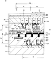
- FIG. 3 shows a first embodiment of a solid-state imaging device according to the present technology, that is, a back-illuminated CMOS solid-state imaging device.
- the back-illuminated CMOS solid-state imaging device is a CMOS solid-state imaging device having a light receiving portion disposed above the circuit portion and higher sensitivity and lower noise than the front-illuminated type.
- the first semiconductor chip unit 26 in which the pixel array 23 and the control circuit 24 are formed, and the logic circuit 25 are formed, similar to the solid-state imaging device 1a in FIG. 2A. It has a laminated semiconductor chip 32 to which the second semiconductor chip portion 28 is bonded. The first semiconductor chip portion 26 and the second semiconductor chip portion 28 are bonded so that the multilayer wiring layers described later face each other and the connection wirings are directly joined.
- the first semiconductor chip portion 26 is a two-dimensional array of a plurality of pixels comprising a photodiode PD serving as a photoelectric conversion portion and a plurality of pixel transistors Tr1 and Tr2 on a first semiconductor substrate 33 made of thinned silicon.
- An array of pixel arrays 34 is formed.
- a plurality of MOS transistors constituting the control circuit 24 are formed on the semiconductor substrate 33.
- a multilayer wiring layer 37 in which a plurality of, in this example, five wirings 35 [35a to 35d] and 36 made of metals M1 to M5 are arranged via an interlayer insulating film 53 is formed. .
- the wirings 35 and 36 are copper (Cu) wirings formed by a dual damascene method.
- a light shielding film 39 is formed including an optical black region 41 through an insulating film 38, and a color filter 44 and an on-semiconductor are formed on the effective pixel array 42 through a planarizing film 43.
- a chip lens 45 is formed.
- An on-semiconductor chip lens 45 can also be formed on the optical black region 41.
- the pixel transistors Tr1 and Tr2 are representative of a plurality of pixel transistors.
- FIG. 3 schematically shows the pixels of the pixel array 34, but FIG. 4 shows details of one pixel.
- the photodiode PD is formed on the thinned semiconductor substrate 33.
- the photodiode PD is formed, for example, having an n-type semiconductor region 46 and a P-type semiconductor region 47 on the substrate surface side.
- a P-type semiconductor region 48 is formed on the surface of the substrate constituting the pixel via a gate insulating film, and pixel transistors Tr1 and Tr2 are formed by the gate electrode 48 and a pair of source / drain regions 49.
- the pixel transistor Tr1 adjacent to the photodiode PD corresponds to the floating diffusion FD.
- Each unit pixel is separated by an element isolation region 51.
- the element isolation region 51 is formed, for example, in an STI (Shallow Trench Isolation) structure in which an insulating film such as a SiO 2 film is embedded in a groove formed in a substrate.
- the corresponding pixel transistor and the wiring 35, and the adjacent upper and lower wirings 35 are connected via the conductive via 52. Furthermore, the connection wiring 36 made of the fifth-layer metal M5 is formed facing the joint surface 40 with the second semiconductor chip portion 28. The connection wiring 36 is connected to a required wiring 35d of the fourth layer metal M4 through the conductive via 52.
- logic circuits 55 constituting peripheral circuits are formed in the regions to be the respective semiconductor chip portions of the second semiconductor substrate 54 made of silicon.
- the logic circuit 55 is formed by a plurality of MOS transistors Tr11 to Tr14 including CMOS transistors.
- wirings 57 [57a to 57c] and 58 of a plurality of layers, in this example, four layers of metals M11 to M14 are provided via an interlayer insulating film 56.
- the arranged multilayer wiring layer 59 is formed.
- the wirings 57 and 58 are copper (Cu) wirings by a dual damascene method.
- each MOS transistor Tr11, Tr12 has a gate electrode 62 in a semiconductor well region on the surface side of the second semiconductor substrate 54 via a pair of source / drain regions 61 and a gate insulating film. Formed.
- the MOS transistors Tr11 and Tr12 are isolated by, for example, an element isolation region 63 having an STI structure.
- the MOS transistors Tr11 to Tr14 and the wiring 57 and the adjacent upper and lower wirings 57 are connected through the conductive via 64. Furthermore, a connection wiring 58 made of the fourth layer metal M14 is formed facing the joint surface 40 with the first semiconductor chip portion 26. The connection wiring 58 is connected to a required wiring 57c of the third layer metal M13 through the conductive via 64.
- the first semiconductor chip portion 26 and the second semiconductor chip portion 28 are electrically connected by directly connecting the connection wirings 36 and 58 facing the bonding surface 40 so that the multilayer wiring layers 37 and 59 face each other. Connected to.
- the interlayer insulating film 66 in the vicinity of the junction is formed of a combination of a Cu diffusion barrier insulating film for preventing Cu diffusion of Cu wiring and an insulating film having no Cu diffusion barrier property, as will be described later in a manufacturing method. Direct connection of the connection wirings 36 and 58 by Cu wiring is performed by thermal diffusion bonding. Bonding between the interlayer insulating films 66 other than the connection wirings 36 and 58 is performed by plasma bonding or an adhesive.
- an extremely thin uniform insulating thin film 900 is formed on the surfaces of the multilayer wiring layers 37 and 59, and the plasma is formed. A method of joining by joining or the like is also possible.
- the insulating thin film 900 is not shown in FIG.
- a light shielding layer 68 is formed from the conductive film.
- the light shielding layer 68 of the present embodiment includes a light shielding portion (first conductor) 71 made of a metal M5 in the same layer as the connection wiring 36 on the first semiconductor chip portion 26 side, and a connection on the second semiconductor chip portion 28 side.
- the light shielding portion (second conductor) 72 is formed of the metal M14 in the same layer as the wiring 58.
- FIG. 7A to FIG. 7C are configuration diagrams showing a light shielding portion of the solid-state imaging device of the present embodiment.
- the light shielding portions 71 of the present embodiment are formed in a layout arranged in a horizontal stripe shape having a plurality of openings 73 at a predetermined pitch when viewed from above.
- the width of the light shielding part 71 is wider than the width of the opening 73, but the width of the opening 73 may be wider than the width of the light shielding part 71.
- the light shielding portions 72 of the present embodiment are formed in a layout arranged in a horizontal stripe shape having a plurality of openings 74 at a predetermined pitch.
- the light shielding part 72 is formed at a position that closes the opening 73 of the light shielding part 71 and having a width wider than the width of the opening 73.
- the light shielding layer 68 after the light shielding portions 71 and 72 are joined is configured to overlap with the light shielding portions 71 and 72 being uniformly closed when viewed from above. That is, the area where the first conductor of the light shielding part 71 and the second conductor of the light shielding part 72 are formed is arranged in a size larger than the area where the pixel array 23 is formed.
- the width of the light shielding part 71 is formed wider than the width of the light shielding part 72, but the width of the light shielding part 72 may be formed wider than the width of the light shielding part 71.
- region of the joining surface 40 in which the conductor of the light-shielding part 71 and the light-shielding part 72 is formed can also have a clearance gap partially.
- the light shielding part 71 and the light shielding part 72 that closes the opening 73 are formed so as to partially overlap each other.
- the connection wirings 36 and 58 are directly joined, the light shielding parts 71 and 72 are directly joined at the overlapping portions at the same time.
- the light shielding portions 71 and 72 are formed such that one is a wiring having an opening 73 and the other is a shape covering the opening 73, has a larger area than the opening 73 and partially overlaps.
- the shape of the opening part 73 which concerns on this technique can consider various shapes, and is not restricted to the horizontal stripe shape of FIG. 7A.
- the light shielding layer 68 is preferably fixed at a potential, for example, a ground potential is applied to stabilize the potential.
- the potential can be fixed on the first semiconductor substrate 33 side, the second semiconductor substrate 54 side, or both.
- FIGS. 11 to 13 are steps on the side of the second semiconductor chip having the logic circuit
- FIGS. 14 to 16 are junctions. The subsequent steps are shown.
- a semiconductor well region 30 is formed in a region to be each semiconductor chip portion of a first semiconductor wafer (hereinafter referred to as a semiconductor substrate) 33 made of silicon, for example, and each pixel is formed in the semiconductor well region 30.
- a photodiode PD serving as a photoelectric conversion portion is formed.
- the element isolation region 51 (see FIG. 4) can be formed and placed first.
- Each photodiode PD is formed extending in the depth direction of the semiconductor well region 30.
- the photodiode PD is formed in the effective pixel array 42 and the optical black region 41 that constitute the pixel array 34.
- a plurality of pixel transistors constituting each pixel are formed on the surface 33a side of the semiconductor well region 30.
- the pixel transistor can be composed of, for example, a transfer transistor, a reset transistor, an amplification transistor, and a selection transistor.
- the pixel transistors Tr1 and Tr2 are shown as representatives.
- each of the pixel transistors Tr1 and Tr2 is formed to have a pair of source / drain regions and a gate electrode formed through a gate insulating film.
- wirings 35 [35a, 35b, 35c, 35d] made of a plurality of layers, in this example, four-layer metals M1 to M4 are provided via the interlayer insulating film 53, including the conductive vias 52.
- the wiring 35 can be formed by a dual damascene method. That is, via-first connection holes and wiring grooves are simultaneously formed in the interlayer insulating film 53, a Cu diffusion barrier metal film and a Cu seed film for preventing Cu diffusion are formed, and then a Cu material layer is embedded by plating.
- the Cu diffusion barrier metal film include Ta, TaN, Ti, TiN, W, WN, Ru, TiZrN, and alloy films containing these.
- an excessive Cu material layer is removed by a CMP (Chemical Mechanical Polishing) method, and a Cu wiring integrated with the planarized conductive via is formed. Thereafter, although not shown, a Cu diffusion barrier insulating film is formed.
- a Cu diffusion barrier insulating film for example, an insulating film such as SiN, SiC, siCN, or SiON can be used. By repeating this process, wirings 35a to 35d made of four layers of metals M1 to M4 are formed.
- a first insulating film 76 not having a Cu diffusion barrier property, a second insulating film 77 not having a Cu diffusion barrier property, and a Cu diffusion barrier insulating film 75 are sequentially formed.
- the first insulating film 76 and the second insulating film 77 are formed of a SiO2 film, a SiCOH film, or the like.
- As the Cu barrier insulating film 75 for example, an insulating film such as SiN, SiC, SiCN, or SiON can be used as described above.
- the Cu diffusion barrier insulating film 75, the first insulating film 76, and the second insulating film 77 correspond to the interlayer insulating film 53.
- the Cu diffusion barrier insulating film 75, the second insulating film 77, and the first insulating film 76 on the outermost surface are patterned to selectively form via holes 80.
- the second insulating film 77 is patterned to selectively form an opening 78. That is, patterning is performed so as to have an opening 78 in a portion corresponding to the light shielding portion 71 (portion excluding the opening 73) to be formed, an opening 79 in a portion corresponding to the connection wiring 36 to be formed, and a via hole 80. .
- the light shielding part 71 having the opening 73 by embedding the Cu material in the openings 78 and 79 and the via hole 80 using the dual damascene method Conductive vias 52 and connection wirings 36 connected to the wirings 35d are formed.
- the light shielding portion 71 and the connection wiring 36 are formed of the fifth layer metal M5.
- the multilayer wiring layer 37 is formed by the wirings 35a to 35d made of the metals M1 to M5, the connection wiring 36, the light shielding portion 71, the interlayer insulating film 53, and the insulating films 75 to 77.
- the wiring 35d1 of the four layers of metal M4 connected to the connection wiring 36 is sufficiently extended to the light shielding part 71 side so that the emitted light from the logic circuit side does not leak to the photodiode PD side. It is preferable to form in an area overlapping with 71.
- an extremely thin uniform insulating thin film 900 is formed on the light shielding part 71 and the connection wiring 36.
- a semiconductor well region 50 is formed in a region to be each semiconductor chip portion of a second semiconductor wafer (hereinafter referred to as a semiconductor substrate) 54 made of silicon.
- a plurality of MOS transistors Tr11 to Tr14 constituting the logic circuit 55 are formed in the semiconductor well region 50.
- the MOS transistors Tr11 to Tr14 are shown as representatives.
- the element isolation region 63 (see FIG. 5) can be formed and placed first.
- a plurality of layers, in this example, three layers of metal M11 to M13, wirings 57 [57a, 57b, 57c] including conductive vias 64 are formed on the upper surface side of the semiconductor substrate 54 via an interlayer insulating film 56.
- the wiring 57 can be formed by a dual damascene method. In other words, via-first connection holes and wiring grooves are simultaneously formed in the interlayer insulating film, a Cu diffusion barrier metal film and a Cu seed film for preventing Cu diffusion are formed, and then a Cu material layer is embedded by plating.
- the Cu diffusion barrier metal film include Ta, TaN, Ti, TiN, W, WN, Ru, TiZrN, and alloy films containing these.
- an excessive Cu material layer is removed by a CMP (Chemical Mechanical Polishing) method, and a Cu wiring integrated with the planarized conductive via is formed. Thereafter, although not shown, a Cu diffusion barrier insulating film is formed.
- a Cu diffusion barrier insulating film for example, an insulating film such as SiN, SiC, siCN, or SiON can be used.
- a first insulating film 82 not having a Cu diffusion barrier property, a second insulating film 83 not having a Cu diffusion barrier property, and a Cu diffusion barrier insulating film 81 are sequentially formed.
- the first insulating film 82 and the second insulating film 83 are formed of a SiO2 film, a SiCOH film, or the like.
- As the Cu barrier insulating film 81 for example, an insulating film such as SiN, SiC, SiCN, or SiON can be used as described above.
- the Cu diffusion barrier insulating film 81, the first insulating film 82, and the second insulating film 83 correspond to an interlayer insulating film.
- the via diffusion is first performed using lithography and etching techniques, and the Cu diffusion barrier insulating film 81, the second insulating film 83, and the first insulating film 82 on the outermost surface are patterned to selectively form via holes 86.
- the second insulating film 83 is patterned to selectively form openings 84 and 85.
- the opening 84 is formed at a position that covers the opening 73 of the light shielding part 71 on the first semiconductor chip side.
- the opening 84 covers the opening 73 of the light shielding part 71 and partially overlaps the light shielding part 71 so that light leakage due to misalignment does not occur when the first semiconductor substrate and the second semiconductor substrate are bonded later. It is desirable to form in a size. That is, patterning is performed so as to have a portion of the opening 84 corresponding to the light shielding portion 72 to be formed, a portion of the opening 85 corresponding to the connection wiring 58 to be formed, and the via hole 86.
- a Cu material is embedded in the openings 84 and 85 and the via hole 86 using the dual damascene method to connect to the light shielding portion 72 and the wiring 57c.
- Conductive vias 64 and connection wirings 58 are formed.
- the light shielding portion 72 and the connection wiring 58 are formed of the fourth layer metal M14.
- a multilayer wiring layer 59 is formed by the wirings 57a to 57c, the connection wiring 58, the light shielding portion 72, the interlayer insulating film 56, and the insulating films 81 to 83 made of the metals M11 to M13.
- an extremely thin uniform insulating thin film 901 is formed on the light shielding portion 72 and the connection wiring 58.
- the first semiconductor substrate 33 and the second semiconductor substrate 54 are electrically connected to each other with the multilayer wiring layers facing each other and the connection wirings 36 and 58 are in direct contact with each other.
- the first semiconductor substrate 33 and the second semiconductor substrate 54 are bonded. That is, the first and second semiconductor substrates 33 and 54 are physically joined and electrically connected.
- the light shielding part 71 and the light shielding part 72 are also directly joined at the overlapping portion. That is, the connection wirings 36 and 58 and the light shielding portions 71 and 72 are thermally diffused and bonded by heat treatment.
- the heat treatment temperature at this time can be about 100 ° C. to 500 ° C.
- the insulating films that are interlayer insulating films are subjected to surface treatment to perform plasma bonding. Note that the insulating films which are interlayer insulating films can be bonded to each other with an adhesive.
- the first conductor of the light shielding portion 71 and the second conductor of the light shielding portion 72 are made of copper which is a conductor by first sandwiching an insulating film between the bonding surfaces 40 and then applying heat. Are connected in the vicinity of the joint surface 40. Therefore, the first conductor and the second conductor are arranged closer to the bonding surface 40 than the logic circuit 55 and the wiring 35 formed in the first semiconductor chip 26 and the second semiconductor chip, respectively.
- the first semiconductor substrate 33 is thinned by grinding and polishing using a CMP method or the like so that the required film thickness of the photodiode PD remains from the back side.
- a light shielding film 39 is formed on the thinned surface through the insulating film 38 so as to cover the photodiode PD corresponding to the optical black region. Further, the color filter 44 and the on-semiconductor chip lens 45 are formed on the photodiode PD corresponding to the effective pixel array via the planarizing film 43.
- a semiconductor chip is formed by separating the bonded first semiconductor substrate 33 and second semiconductor substrate s54 into respective semiconductor chips, and the target solid-state imaging device 31 shown in FIG. 3 is obtained.
- a material having high conductivity, high light shielding properties, and easy joining is desirable.
- a material having such properties in addition to Cu, a single material such as Al, W, Ti, Ta, Mo, Ru, or an alloy can be used.
- the film thickness of the light shielding layer 68 in this example, the film thickness of the light shielding parts 71 and 72, is desirably determined according to the wavelength of light on the second semiconductor chip part 28 side that emits light.
- the thickness of the light shielding layer 68, and hence the thickness of the light shielding portions 71 and 72 can be about 50 nm to 800 nm.
- the first conductor 71 and the second conductor are formed in the vicinity of the joint surface 40 between the first semiconductor chip unit 26 and the second semiconductor chip unit 28.
- the light shielding layer 68 and the shield layer against electrical noise are formed only by the conductor 72.
- the first conductor 71 has a higher area ratio in contact with the joint surface 40 than the second conductor 72 and is asymmetric. For this reason, according to the solid-state imaging device 31 and the manufacturing method thereof, it is possible to realize wafer bonding of a conductive film having a high area ratio and suppress generation of voids on the bonding surface 40.
- the solid-state imaging device 31 that improves the image quality by suppressing the generation of voids on the joint surface 40.
- the area ratio in contact with the bonding surface 40 may be an asymmetrical difference between the first conductor 71 and the second conductor 72, and the second conductor 72 is more than the first conductor 71. It may be high.
- asymmetric means a layout in which the Cu area ratio on the lower substrate side is 30% or less and the Cu area ratio on the upper substrate is 70% or more, and 100% can be shielded from light after bonding.
- the area ratio of the higher substrate is desirably 70% or more, and more preferably 87% or more.
- the area ratio of the lower substrate is desirably 30% or less, and more preferably 13% or less.
- a dummy conductor may be disposed in the vicinity of the bonding surface 40 instead of the first conductor 71 or the second conductor 72.
- the metal M5 in the same layer as the connection wirings 36 and 58 near the junction between the first semiconductor chip unit 26 and the second semiconductor chip unit 28. , M14 is formed.
- the light shielding layer 68 can suppress light emitted by hot carriers from the MOS transistor of the logic circuit 55 of the second semiconductor chip unit 28 from entering the pixel array on the first semiconductor chip unit 26 side. Therefore, the adverse effect of light emission due to hot carriers is suppressed, so that dark current and random noise can be suppressed.
- the light shielding layer 68 is formed of the same metal M5 and M14 as the connection wirings 36 and 58, the bonded semiconductor compared to the prior art.
- the thickness of the entire chip can be reduced, and the solid-state imaging device 31 can be made thinner.
- the solid-state imaging device 31 with less dark current and random noise can be provided without increasing the thickness of the entire semiconductor chip.
- the wiring, the connection wiring, and the light shielding layer can be formed at the same time. It is possible to manufacture a solid-state imaging device with low dark current and random noise at low cost.
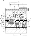
- Solid-State Imaging Device of Second Embodiment> A second embodiment of the solid-state imaging device according to the present technology will be described with reference to FIG. This embodiment is different from the first embodiment of FIG. 16 in that the connection wiring 36 and the wiring 57c of the metal M13 are connected by the light shielding portion 72 without forming the conductive via 64 of the wiring layer 58 and the light shielding portion 72. This is the point of connection.
- the solid-state imaging device 31 of the present embodiment has the same effect as the solid-state imaging device 31 of the first embodiment, and further has an advantage that the manufacturing process and the manufacturing cost can be reduced by not forming the conductive via 64. is there.
- Solid-State Imaging Device of Third Embodiment> A third embodiment of the solid-state imaging device according to the present technology will be described with reference to FIG. This embodiment is different from the first embodiment of FIG. 16 in that the wiring area ratio of the wiring 902 is set in the same manner as the light shielding layer 68 even when the connection wiring 36 and the wiring 58 are used as power supply wiring. The wiring area ratio of the wiring 903 is lowered and the wirings 902 and 903 are joined asymmetrically.
- the solid-state imaging device 31 of the present embodiment also has the same effect as the solid-state imaging device 31 of the first embodiment, and in particular, the area ratio of the wirings 902 and 903 in addition to the light shielding layer 68 is asymmetrical, and the other area By increasing the ratio, voids generated at the time of joining can be further suppressed.
- Solid-State Imaging Device of Fourth Embodiment> A fourth embodiment of the solid-state imaging device according to the present technology will be described with reference to FIG. This embodiment is different from the first embodiment of FIG. 16 in that two layers of the second semiconductor substrate 54 are stacked in the second semiconductor chip portion 28. In the interlayer insulating film and the second semiconductor substrate 54 bonded to the interlayer insulating film, the wirings 57 c are electrically connected to each other through the wiring 904.
- the solid-state imaging device 31 of this embodiment also has the same effect as the solid-state imaging device 31 of the first embodiment. Note that the stack of the semiconductor substrates of the solid-state imaging device according to the present technology is not limited to three layers or less, and may be four layers or more.
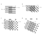
- Solid-State Imaging Device of Fifth Embodiment> A fifth embodiment of the solid-state imaging device according to the present technology will be described with reference to FIGS. 20 to 22. This embodiment is different from the first embodiment of FIG. 16 in that the planar layout of the light shielding layer 68 is arranged in an oblique stripe type or a checkered type other than the horizontal stripe type shown in FIG. It is.
- FIG. 20A shows a case where the planar shape of the light shielding layer 68 is a horizontal stripe type similar to that of the first embodiment.
- variety of each vertical direction of the light shielding parts 71 and 72 may be the same, and may differ.
- FIG. 20B shows a case where the planar shape of the light shielding layer 68 is an oblique stripe type arranged from the upper left to the lower right.
- FIG. 20C shows a case where the planar shape of the light shielding layer 68 is a checkered pattern. In this checkered pattern, a plurality of rectangular light shielding portions 72 having a larger area than the opening 73 are arranged so as to cover the plurality of rectangular openings 73 formed in the light shielding portion 71. Note that the rectangle includes a square.
- FIG. 20D shows a case where the planar shape of the light shielding layer 68 is an oblique checkered pattern obtained by rotating the checkered pattern of FIG. 20C by a predetermined angle in the clockwise
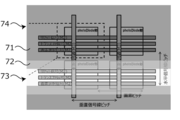
- FIG. 21 is an enlarged view showing a signal line layout of the pixel array of the solid-state imaging device of the present embodiment.
- a plurality of photodiodes are arranged in parallel in the vertical and horizontal directions.
- a plurality of reset signal lines M21, transfer signal lines M22, and pixel selection signal lines M23 are horizontally arranged at predetermined pitches in the horizontal direction.
- a plurality of vertical signal lines M3 are vertically arranged at a predetermined pitch in the vertical direction.
- 22A to 22C are configuration diagrams for explaining the layout of the shield layer of the solid-state imaging device according to the present embodiment.
- the light shielding layer (shield layer) 68 shown in FIG. 22A is arranged in a vertical stripe type in which light shielding portions 71 and 72 have a plurality of openings 73 and 74 at a predetermined pitch when viewed from above.
- a difference occurs between the vertical signal lines M3 and the shield layer 68, and the total capacity of each vertical signal line M3 may vary.
- the shield layer 68 shown in FIG. 22B has light shielding portions 71 and 72 arranged in a horizontal stripe shape having a plurality of openings 73 and 74 at a predetermined pitch when viewed from above.
- a difference occurs between the horizontal control lines M21 to M23 and the shield layer 68, and the total capacity of the horizontal signal lines M21 to M23 may vary.
- the light shielding portions 71 and 72 are arranged in an oblique stripe shape having a plurality of openings 73 at a predetermined pitch from the upper left to the lower right as viewed from above.
- the interlayer capacitance between each vertical signal line M3 and the shield layer 68 per horizontal control line M21 to M23 is uniform, and the total capacitance It becomes possible to suppress the variation of. Therefore, the band noise of the solid-state imaging device can be further reduced as compared with other vertical and horizontal stripe types.
- the pitch repeat direction of the stripe-type or checkered-type shield layer 68 is arranged obliquely with respect to the horizontal signal lines M21 to M3 and the vertical signal lines M3 of the logic circuit 55. Since the capacitance between the shield layer 68 and each signal line can be made uniform throughout the pixel array 23, the electrical noise of the solid-state imaging device 31 can be reduced. Furthermore, as a countermeasure against reflection, the influence of capacitive coupling can be dispersed by arranging the shield layer 68 in an oblique stripe shape so as not to be orthogonal to all signal lines.
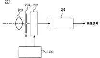
- FIG. 23 is a diagram illustrating an electronic apparatus according to the present technology.
- the above-described solid-state imaging device according to the present technology can be applied to electronic devices such as a camera system such as a digital camera or a video camera, a mobile phone having an imaging function, or other devices having an imaging function. .
- FIG. 23 shows a sixth embodiment applied to a camera as an example of an electronic apparatus according to the present technology.
- the camera according to the present embodiment is an example of a video camera capable of capturing still images or moving images.
- a camera 201 according to this embodiment includes a solid-state imaging device 202, an optical system 203 that guides incident light to a light receiving sensor unit of the solid-state imaging device 202, and a shutter device 204. Furthermore, a drive circuit 205 that drives the solid-state imaging device 202 and a signal processing circuit 206 that processes an output signal of the solid-state imaging device 202 are included.
- the optical system (optical lens) 203 forms image light (incident light) from the subject on the imaging surface of the solid-state imaging device 202. Thereby, signal charges are accumulated in the solid-state imaging device 202 for a certain period.
- the optical system 203 may be an optical lens system including a plurality of optical lenses.
- the shutter device 204 controls a light irradiation period and a light shielding period for the solid-state imaging device 202.
- the drive circuit 205 supplies a drive signal that controls the transfer operation of the solid-state imaging device 202 and the shutter operation of the shutter device 204.
- Signal transfer of the solid-state imaging device 202 is performed by a drive signal (timing signal) supplied from the drive circuit 205.
- the signal processing circuit 206 performs various signal processing.
- the video signal subjected to the signal processing is stored in a storage medium such as a memory or output to a monitor.
- the back-illuminated solid-state imaging device 202 since the back-illuminated solid-state imaging device 202 according to the present technology described above is provided, the light emitted from the hot carrier from the MOS transistor of the logic circuit is not incident on the pixel array side. , Dark current and random noise can be suppressed. Therefore, a high-quality electronic device can be provided. For example, a camera with improved image quality can be provided.
- this technique can take the following structures.
- the solid-state imaging device according to (1) wherein a wiring and a connection hole for fixing the potential of the first conductor and the second conductor are formed in the second semiconductor chip. .
- the first conductor and the second conductor are disposed closer to the bonding surface than the logic circuit and the wiring formed in the first semiconductor chip and the second semiconductor chip, respectively.
- (9) The solid-state imaging device according to (1), wherein the area where the first conductor and the second conductor are formed is arranged in a size larger than the area where the pixel array is formed. .
- a plurality of the first conductors and the second conductors are formed, and an arrangement direction of the plurality of first conductors and the plurality of second conductors is determined by the first semiconductor chip and The solid-state imaging device according to (1), wherein the solid-state imaging device has a direction inclined with respect to a direction of a signal line of an analog circuit formed on the second semiconductor chip.
- a first semiconductor chip on which one or a plurality of first conductors and a pixel array are formed; And at least a second semiconductor chip bonded to the first semiconductor chip and having one or more second conductors and logic circuits formed thereon, The first conductor and the second conductor are overlapped and electrically connected at a joint surface between the first semiconductor chip and the second semiconductor chip,
- An electronic apparatus comprising a solid-state imaging device having an area in contact with the bonding surface that is different between the first conductor and the second conductor.
- Solid-state imaging device Pixel 3, 23, 34 Pixel array (pixel region) 4 vertical drive circuit 5 column signal processing circuit 6 horizontal drive circuit 7 output circuit 8, 24, 24-1, 24-2 control circuit 9 vertical signal line 10 horizontal signal line 21, 33 first semiconductor substrate 22, 54 second Semiconductor substrate 25, 55 Logic circuit 26 First semiconductor chip portion 28 Second semiconductor chip portion 30, 50 Semiconductor well region 32 Multilayer semiconductor chip 33a Surfaces 35a-35d, 36, 57a-57c, 58, 902-904 Wiring 37, 59 Multi-layer wiring layer 38 Insulating film 39 Shading film 40 Bonding surface 41 Optical black region 42 Effective pixel array 43 Flattening film 44 Color filter 45 On-semiconductor chip lens 47, 48 P-type semiconductor region 49, 61 Source / drain region 51 , 63 Element isolation regions 52, 64 Conductive vias 53, 56, 66 Interlayer insulating film 62 Gate electrode 68 Light-shielding layer 71 Light-shielding part (first conductor) 72 Light-shield
Abstract
Provided is a solid-state image pickup device wherein, in a bonding surface between a plurality of semiconductor chips, wafer bonding of conductive films at a high area ratio is achieved, and generation of voids can be suppressed.
A solid-state image pickup device 31 at least includes: a first semiconductor chip 26 wherein one or a plurality of first conductive bodies 71 and a pixel array 34 are formed; and a second semiconductor chip section 28, which is connected to the first semiconductor chip 26, and in which one or a plurality of second conductive bodies 72 and a logic circuit 55 are formed. At a bonding surface 40 between the first semiconductor chip 26 and the second semiconductor chip section 28, the first conductive body 71 and the second conductive body 72 overlap each other and are electrically connected to each other, and a first conductive body 71 area in contact with the bonding surface 40, and a second conductive body 72 area in contact with the bonding surface are different from each other.
Description
本技術は、固体撮像装置、固体撮像装置の製造方法および電子機器に関し、特に、複数の半導体チップを接合して構成される固体撮像装置の技術に関する。
The present technology relates to a solid-state imaging device, a manufacturing method of the solid-state imaging device, and an electronic apparatus, and particularly relates to a technology of a solid-state imaging device configured by joining a plurality of semiconductor chips.
近年、デジタルカメラの普及がますます進んでいる。これに伴い、デジタルカメラの中心部品である固体撮像装置(イメージセンサ)の需要がますます高まっている。固体撮像装置の性能面においては、高画質化および高機能化を実現するための技術開発が進められている。
In recent years, digital cameras have become more popular. Along with this, there is an increasing demand for solid-state imaging devices (image sensors), which are the central components of digital cameras. In terms of performance of the solid-state imaging device, technological development for realizing high image quality and high functionality is underway.
一方で、撮像機能を有する携帯端末(携帯電話機、PDA(Personal Digital Assistant)、ノートPC(Personal Computer)やタブレットPC等)の普及も進んでいる。これに伴い、これら携帯端末の携帯性を高めるために、固体撮像装置やそれを構成する部品の小型化、軽量化、および薄型化が進められている。さらに、これら携帯端末の普及拡大のために、固体撮像装置やそれを構成する部品の低コスト化も進められている。
On the other hand, mobile terminals (such as mobile phones, PDAs (Personal Digital Assistants), notebook PCs (Personal Computers), and tablet PCs) having an imaging function are also spreading. Along with this, in order to improve the portability of these portable terminals, the solid-state imaging device and the components constituting it have been reduced in size, weight, and thickness. Furthermore, in order to increase the spread of these portable terminals, the cost of solid-state imaging devices and parts constituting them is being reduced.
一般的に、例えば、CMOS(Complementary Metal Oxide Semiconductor)イメージセンサなどの固体撮像装置は、シリコン基板の受光面側に光電変換部や増幅回路、多層配線層を形成し、その上にカラーフィルタやオン半導体チップマイクロレンズを形成することで構成される。さらに、その受光面側には、接着剤等のスペーサによりカバーガラスが貼り合わせられる。また、その受光面の反対側には、端子が形成される。
In general, for example, a solid-state imaging device such as a CMOS (Complementary Metal Oxide Semiconductor) image sensor forms a photoelectric conversion unit, an amplifier circuit, and a multilayer wiring layer on a light receiving surface side of a silicon substrate, and a color filter and an on-layer are formed thereon. It is configured by forming a semiconductor chip microlens. Further, a cover glass is bonded to the light receiving surface side by a spacer such as an adhesive. A terminal is formed on the opposite side of the light receiving surface.
この固体撮像装置には、出力される信号に対して所定の処理を行う信号処理回路が接続される。固体撮像装置の多機能化に伴い、信号処理回路で行われる処理は増える傾向にある。
This signal processing device is connected to a signal processing circuit that performs predetermined processing on the output signal. With the increasing functionality of solid-state imaging devices, the processing performed in signal processing circuits tends to increase.
このように複数の半導体チップが接続された構成を小型化するために、様々な手段が講じられている。例えば、SiP(System in Package)技術により、複数の半導体チップを1つのパッケージ内に封止することが行われている。これにより、実装面積を小さくすることができ、全体の構成の小型化を実現することができる。しかしながら、SiPでは半導体チップ間を接続する配線によって伝送距離が長くなり、高速動作が妨げられるおそれがある。
In order to reduce the size of the configuration in which a plurality of semiconductor chips are connected in this way, various means have been taken. For example, a plurality of semiconductor chips are sealed in one package by SiP (System-in-Package) technology. Thereby, a mounting area can be made small and the size reduction of the whole structure can be implement | achieved. However, in SiP, the transmission distance becomes longer due to the wiring connecting the semiconductor chips, which may hinder high-speed operation.
ところで、例えば特許文献1には、画素領域(画素アレイ)を含む第1の半導体基板と、ロジック回路を含む第2の半導体基板とを貼り合わせて接合することで構成された固体撮像装置が記載されている。このような構成によれば、信号を高速で伝送することが可能となる。この固体撮像装置は、共に半製品状態の画素アレイを備えた第1の半導体チップ部と、ロッジク回路を備えた第2の半導体チップ部とを貼り合わせ、第1の半導体チップ部を薄膜化した後、画素アレイとロジック回路の接続がなされる。接続は、第1の半導体チップ部の所要の配線に接続する接続導体と、第1の半導体チップ部を貫通して第2の半導体チップ部の所要の配線に接続する貫通接続導体と、両接続導体を繋ぐ連結導体からなる接続配線を形成して行われる。その後、完成品状態にして半導体チップ化して、裏面照射型の固体撮像装置として構成される。
Incidentally, for example, Patent Document 1 describes a solid-state imaging device configured by bonding and bonding a first semiconductor substrate including a pixel region (pixel array) and a second semiconductor substrate including a logic circuit. Has been. According to such a configuration, a signal can be transmitted at high speed. In this solid-state imaging device, a first semiconductor chip portion having a pixel array in a semi-finished product state is bonded to a second semiconductor chip portion having a logic circuit, and the first semiconductor chip portion is thinned. Thereafter, the pixel array and the logic circuit are connected. The connection includes a connection conductor connected to the required wiring of the first semiconductor chip portion, a through connection conductor passing through the first semiconductor chip portion and connected to the required wiring of the second semiconductor chip portion, and both connections This is performed by forming a connection wiring composed of a connecting conductor that connects the conductors. After that, a finished product is formed into a semiconductor chip, which is configured as a back-illuminated solid-state imaging device.
一方、上記第1の半導体チップ部と第2の半導体チップ部を接合してなる固体撮像装置において、さらに新たな技術として、特許文献2の固体撮像装置では、貫通接続導体による電気的接続法ではなく、両半導体チップ部面に銅(Cu)電極を取り出して接続させる方法が考えられている。
On the other hand, in the solid-state imaging device formed by joining the first semiconductor chip portion and the second semiconductor chip portion, as a new technology, in the solid-state imaging device of Patent Document 2, an electrical connection method using a through-connection conductor is used. Instead, a method of taking out and connecting a copper (Cu) electrode to both semiconductor chip surface is considered.
また、特許文献3の固体撮像装置では、上記銅(Cu)電極が遮光層に用いられている。これにより、ロジック回路のトランジスタからのホットキャリアによる発光が遮光層で遮られ、画素アレイ側への入射が抑制される。また、接合後の半導体チップ全体の厚みも抑制されるとされている。
Further, in the solid-state imaging device of Patent Document 3, the copper (Cu) electrode is used for the light shielding layer. As a result, light emission from the hot carriers from the transistors of the logic circuit is blocked by the light blocking layer, and incidence on the pixel array side is suppressed. In addition, the thickness of the entire semiconductor chip after bonding is also suppressed.
上記特許文献3のように銅電極を遮光層に用いるには、この銅電極の被覆率(面積比率)をある一定以上に高く設定する必要がある。
In order to use a copper electrode for the light shielding layer as in Patent Document 3, it is necessary to set the coverage (area ratio) of the copper electrode to be higher than a certain level.
しかしながら、面積比率をある一定以上に高く設定すると、第1の半導体ウェハと第2の半導体ウェハの接合において、部分的に接合できない領域となりボイド(気泡)が形成されてしまうという問題がある。さらに、ボイドが形成されると、その部分の接合強度が無いため、ウェハ(Wafer)接合後に行われる第1の半導体ウェハのSi基板を薄くする工程に於いて、剥離を引き起こすという問題がある。
However, when the area ratio is set higher than a certain level, there is a problem that voids (bubbles) are formed when the first semiconductor wafer and the second semiconductor wafer are joined, resulting in a region that cannot be partly joined. Further, when the void is formed, there is no bonding strength at that portion, and therefore there is a problem that peeling is caused in the process of thinning the Si substrate of the first semiconductor wafer performed after the wafer bonding.
このように、接合できない領域が発生するのは、銅電極の面積比率の割合を高くすることにより、Wafer To Wafer Bonding時のBonding-Wave速度が不均一となり、結果としてウェハ外周部に於いて、接合速度が相対的に遅くなる箇所が発生し、接合できない領域、つまりボイドが形成されると考えられている。
In this way, the region that cannot be bonded is generated by increasing the ratio of the area ratio of the copper electrode, so that the bonding-wave speed at the time of Wafer To Wafer Bonding becomes uneven, and as a result, at the outer periphery of the wafer, It is considered that a portion where the joining speed becomes relatively slow occurs, and a region that cannot be joined, that is, a void is formed.
本技術は、このような状況に鑑みてなされたものであり、複数の半導体チップの接合面で、高面積比率の導電膜のウェハ接合を実現させてボイドの発生を抑制できる固体撮像装置を提供することを目的とする。
The present technology has been made in view of such a situation, and provides a solid-state imaging device capable of suppressing the generation of voids by realizing wafer bonding of a conductive film having a high area ratio at a bonding surface of a plurality of semiconductor chips. The purpose is to do.
上記課題を解決するため、本技術の一例である固体撮像装置は、一つまたは複数の第1の導電体および画素アレイが形成された第1の半導体チップと、第1の半導体チップと接合され、一つまたは複数の第2の導電体およびロジック回路が形成された第2の半導体チップと、を少なくとも含み、第1の半導体チップと第2の半導体チップとの接合面で、第1の導電体と第2の導電体とが重なり合って電気的に接続され、接合面に接する面積が、第1の導電体と第2の導電体とで異なる。
In order to solve the above problem, a solid-state imaging device as an example of the present technology is bonded to a first semiconductor chip on which one or a plurality of first conductors and a pixel array are formed, and the first semiconductor chip. , At least a second semiconductor chip on which one or a plurality of second conductors and a logic circuit are formed, and the first conductive at the joint surface between the first semiconductor chip and the second semiconductor chip. The body and the second conductor overlap and are electrically connected, and the area in contact with the bonding surface is different between the first conductor and the second conductor.
また、本技術の一例である固体撮像装置の製造方法は、一つまたは複数の第1の導電体および画素アレイを第1の半導体チップに形成するステップと、一つまたは複数の第2の導電体およびロジック回路を第2の半導体チップに形成するステップと、第1の半導体チップに形成された第1の導電体と第2の半導体チップに形成された第2の導電体とを重なり合わせて電気的に接続するステップと、を含み、第1の半導体チップと第2の半導体チップとの接合面に接する面積が、第1の導電体と第2の導電体とで異なる。
In addition, a method for manufacturing a solid-state imaging device as an example of the present technology includes a step of forming one or more first conductors and a pixel array on a first semiconductor chip, and one or more second conductors. Forming the body and the logic circuit on the second semiconductor chip, and overlapping the first conductor formed on the first semiconductor chip and the second conductor formed on the second semiconductor chip. The first conductor and the second conductor have different areas in contact with the bonding surface between the first semiconductor chip and the second semiconductor chip.
また、本技術の一例である電子機器は、一つまたは複数の第1の導電体および画素アレイが形成された第1の半導体チップと、第1の半導体チップと接合され、一つまたは複数の第2の導電体およびロジック回路が形成された第2の半導体チップと、を少なくとも含み、第1の半導体チップと第2の半導体チップとの接合面で、第1の導電体と第2の導電体とが重なり合って電気的に接続され、接合面に接する面積が、第1の導電体と第2の導電体とで異なる固体撮像装置を備える。
In addition, an electronic apparatus that is an example of the present technology includes a first semiconductor chip in which one or a plurality of first conductors and a pixel array are formed, and a first semiconductor chip that is bonded to the first semiconductor chip. A second semiconductor chip on which a second conductor and a logic circuit are formed, and the first conductor and the second conductor at a joint surface between the first semiconductor chip and the second semiconductor chip. The solid-state imaging device includes a body that overlaps and is electrically connected, and an area in contact with the joint surface is different between the first conductor and the second conductor.
本技術によれば、複数の半導体チップの接合面で、高面積比率の導電膜のウェハ接合を実現させてボイドの発生を抑制できる固体撮像装置を提供することが可能となる。なお、本技術の効果は、必ずしも上記の効果に限定されるものではなく、本開示中に記載されたいずれかの効果であってもよい。
According to the present technology, it is possible to provide a solid-state imaging device capable of suppressing the generation of voids by realizing wafer bonding of a conductive film having a high area ratio at bonding surfaces of a plurality of semiconductor chips. Note that the effects of the present technology are not necessarily limited to the above effects, and may be any of the effects described in the present disclosure.
以下、本技術を実施するための好適な形態について図面を参照しながら説明する。なお、以下に説明する実施形態は、本技術の代表的な実施形態の一例を示したものであり、これにより本技術の範囲が狭く解釈されることはない。説明は以下の順序で行う。
1.固体撮像装置の構成例
2.固体撮像装置の積層構造例
3.第1実施形態の固体撮像装置
4.第2実施形態の固体撮像装置
5.第3実施形態の固体撮像装置
6.第4実施形態の固体撮像装置
7.第5実施形態の固体撮像装置
8.第6実施形態の電子機器 Hereinafter, preferred embodiments for carrying out the present technology will be described with reference to the drawings. In addition, embodiment described below shows an example of typical embodiment of this technique, and, thereby, the scope of this technique is not interpreted narrowly. The description will be made in the following order.
1. 1. Configuration example of solid-state imaging device 2. Example of laminated structure of solid-state imaging device 3. Solid-state imaging device according to the first embodiment 4. Solid-state imaging device according to the second embodiment 5. Solid-state imaging device according to the third embodiment 6. Solid-state imaging device according to fourth embodiment 7. Solid-state imaging device according to fifth embodiment Electronic device according to sixth embodiment
1.固体撮像装置の構成例
2.固体撮像装置の積層構造例
3.第1実施形態の固体撮像装置
4.第2実施形態の固体撮像装置
5.第3実施形態の固体撮像装置
6.第4実施形態の固体撮像装置
7.第5実施形態の固体撮像装置
8.第6実施形態の電子機器 Hereinafter, preferred embodiments for carrying out the present technology will be described with reference to the drawings. In addition, embodiment described below shows an example of typical embodiment of this technique, and, thereby, the scope of this technique is not interpreted narrowly. The description will be made in the following order.
1. 1. Configuration example of solid-
<1.固体撮像装置の構成例>
図1は、本技術に係る固体撮像装置の構成例を示すブロック図である。 <1. Configuration Example of Solid-State Imaging Device>
FIG. 1 is a block diagram illustrating a configuration example of a solid-state imaging device according to the present technology.
図1は、本技術に係る固体撮像装置の構成例を示すブロック図である。 <1. Configuration Example of Solid-State Imaging Device>
FIG. 1 is a block diagram illustrating a configuration example of a solid-state imaging device according to the present technology.
図1に示すように、固体撮像装置1は、例えば、CMOS(Complementary Metal Oxide Semiconductor)イメージセンサとして構成される。固体撮像装置1は、図示しない半導体基板(例えばSi基板)に複数の画素2が規則的に2次元アレイ状に配列された画素領域(画素アレイ)3と、周辺回路部とを有する。
As shown in FIG. 1, the solid-state imaging device 1 is configured as, for example, a CMOS (Complementary Metal Metal Oxide Semiconductor) image sensor. The solid-state imaging device 1 includes a pixel region (pixel array) 3 in which a plurality of pixels 2 are regularly arranged in a two-dimensional array on a semiconductor substrate (for example, Si substrate) (not shown), and a peripheral circuit unit.
画素2は、光電変換部(例えばフォトダイオード)と、複数の画素トランジスタ(MOSトランジスタ)を有する。複数の画素トランジスタは、例えば、転送トランジスタ、リセットトランジスタ、および増幅トランジスタの3つのトランジスタで構成することができる。また、複数の画素トランジスタは、選択トランジスタを追加して4つのトランジスタで構成することもできる。なお、単位画素の等価回路は周知な技術と同様であるので、詳細な説明は省略する。
The pixel 2 has a photoelectric conversion unit (for example, a photodiode) and a plurality of pixel transistors (MOS transistors). The plurality of pixel transistors can be constituted by three transistors, for example, a transfer transistor, a reset transistor, and an amplification transistor. In addition, the plurality of pixel transistors can be configured by four transistors by adding selection transistors. Since the equivalent circuit of the unit pixel is the same as that of a well-known technique, detailed description thereof is omitted.
また、画素2は、1つの単位画素として構成することもできるし、共有画素構造とすることもできる。この画素共有構造は、複数のフォトダイオードが、フローティングディフュージョン、および複数の転送トランジスタ以外の他のトランジスタを共有する構造である。すなわち、共有画素では、複数の単位画素を構成するフォトダイオードおよび転送トランジスタが、他の1つずつの画素トランジスタを共有して構成される。
In addition, the pixel 2 can be configured as one unit pixel or a shared pixel structure. This pixel sharing structure is a structure in which a plurality of photodiodes share a transistor other than the floating diffusion and the plurality of transfer transistors. That is, in the shared pixel, a photodiode and a transfer transistor that form a plurality of unit pixels are configured by sharing each other pixel transistor.
周辺回路部は、垂直駆動回路4、カラム信号処理回路5、水平駆動回路6、出力回路7、および制御回路8を有する。
The peripheral circuit section has a vertical drive circuit 4, a column signal processing circuit 5, a horizontal drive circuit 6, an output circuit 7, and a control circuit 8.
垂直駆動回路4は、例えばシフトレジスタによって構成される。垂直駆動回路4は、画素駆動配線を選択し、選択された画素駆動配線に画素を駆動するためのパルスを供給し、行単位で画素を駆動する。すなわち、垂直駆動回路4は、画素アレイ3の各画素2を行単位で順次垂直方向に選択走査する。そして、垂直駆動回路4は、垂直信号線9を通して各画素2の光電変換部において受光量に応じて生成された信号電荷に基づく画素信号を、カラム信号処理回路5に供給する。
The vertical drive circuit 4 is constituted by a shift register, for example. The vertical drive circuit 4 selects a pixel drive wiring, supplies a pulse for driving the pixel to the selected pixel drive wiring, and drives the pixels in units of rows. That is, the vertical drive circuit 4 selectively scans each pixel 2 of the pixel array 3 in the vertical direction sequentially in units of rows. The vertical drive circuit 4 supplies the column signal processing circuit 5 with a pixel signal based on the signal charge generated according to the amount of received light in the photoelectric conversion unit of each pixel 2 through the vertical signal line 9.
カラム信号処理回路5は、例えば画素2の列毎に配置される。カラム信号処理回路5は、1行分の画素2から出力される信号に対して画素列毎に、ノイズ除去などの信号処理を行う。具体的には、カラム信号処理回路5は、画素2固有の固定パターンノイズを除去するためのCDS(Correlated Double Sampling)や、信号増幅、A/D(Analog/Digital)変換等の信号処理を行う。カラム信号処理回路5の出力段には、水平選択スイッチ(図示せず)が水平信号線10との間に接続されて設けられる。
The column signal processing circuit 5 is arranged for each column of the pixels 2, for example. The column signal processing circuit 5 performs signal processing such as noise removal for each pixel column on the signal output from the pixels 2 for one row. Specifically, the column signal processing circuit 5 performs signal processing such as CDS (Correlated Double Sampling) for removing fixed pattern noise unique to the pixel 2, signal amplification, A / D (Analog / Digital) conversion, and the like. . At the output stage of the column signal processing circuit 5, a horizontal selection switch (not shown) is provided connected to the horizontal signal line 10.
水平駆動回路6は、例えばシフトレジスタによって構成される。水平駆動回路6は、水平走査パルスを順次出力することによって、カラム信号処理回路5それぞれを順番に選択し、カラム信号処理回路5それぞれからの画素信号を水平信号線10に出力させる。
The horizontal drive circuit 6 is constituted by a shift register, for example. The horizontal drive circuit 6 sequentially selects the column signal processing circuits 5 by sequentially outputting horizontal scanning pulses, and outputs the pixel signals from the column signal processing circuits 5 to the horizontal signal line 10.
出力回路7は、カラム信号処理回路5の各々から水平信号線10を通して順次に供給される信号に対し、信号処理を行って出力する。出力回路7は、例えば、バッファリングだけ行う場合もあるし、黒レベル調整、列ばらつき補正、各種デジタル信号処理等を行う場合もある。
The output circuit 7 performs signal processing on the signals sequentially supplied from each of the column signal processing circuits 5 through the horizontal signal line 10 and outputs the signals. For example, the output circuit 7 may perform only buffering, or may perform black level adjustment, column variation correction, various digital signal processing, and the like.
制御回路8は、入力クロックと、動作モード等を指令するデータを受け取り、また固体撮像装置1の内部情報等のデータを出力する。また、制御回路8は、垂直同期信号、水平同期信号、およびマスタクロックに基づいて、垂直駆動回路4、カラム信号処理回路5および水平駆動回路6等の動作の基準となるクロック信号や制御信号を生成する。そして、制御回路8は、これらの信号を垂直駆動回路4、カラム信号処理回路5、および水平駆動回路6等に入力する。
The control circuit 8 receives an input clock and data for instructing an operation mode, and outputs data such as internal information of the solid-state imaging device 1. In addition, the control circuit 8 receives a clock signal and a control signal that serve as a reference for operations of the vertical drive circuit 4, the column signal processing circuit 5, the horizontal drive circuit 6 and the like based on the vertical synchronization signal, the horizontal synchronization signal, and the master clock. Generate. The control circuit 8 inputs these signals to the vertical drive circuit 4, the column signal processing circuit 5, the horizontal drive circuit 6, and the like.
入出力端子12は、外部と信号のやりとりをする。
The input / output terminal 12 exchanges signals with the outside.
<2.固体撮像装置の積層構造例>
図2AないしCは、本技術に係る固体撮像装置の積層構造例を示す模式図である。図2AないしCを用いて、本技術が適用される固体撮像装置の積層構造例について説明する。 <2. Example of laminated structure of solid-state imaging device>
2A to 2C are schematic views illustrating a stacked structure example of the solid-state imaging device according to the present technology. A stacked structure example of a solid-state imaging device to which the present technology is applied will be described with reference to FIGS. 2A to 2C.
第1の例として、図2Aに示される固体撮像装置1aは、第1の半導体基板21と第2の半導体基板22とから構成される。第1の半導体基板21には、画素アレイ23と制御回路24が搭載される。第2の半導体基板22には、信号処理回路を含むロジック回路25が搭載される。そして、第1の半導体基板21と第2の半導体基板22とが相互に電気的に接続されることで、1つの半導体チップとしての固体撮像装置1aが構成される。
As a first example, the solid-state imaging device 1a shown in FIG. 2A includes a first semiconductor substrate 21 and a second semiconductor substrate 22. A pixel array 23 and a control circuit 24 are mounted on the first semiconductor substrate 21. A logic circuit 25 including a signal processing circuit is mounted on the second semiconductor substrate 22. Then, the first semiconductor substrate 21 and the second semiconductor substrate 22 are electrically connected to each other, whereby the solid-state imaging device 1a as one semiconductor chip is configured.
第2の例として、図2Bに示される固体撮像装置1bは、第1の半導体基板21と第2の半導体基板22とから構成される。第1の半導体基板21には、画素アレイ23が搭載される。第2の半導体基板22には、制御回路24と、信号処理回路を含むロジック回路25が搭載される。そして、第1の半導体基板21と第2の半導体基板22とが相互に電気的に接続されることで、1つの半導体チップとしての固体撮像装置1bが構成される。
As a second example, the solid-state imaging device 1b shown in FIG. 2B includes a first semiconductor substrate 21 and a second semiconductor substrate 22. A pixel array 23 is mounted on the first semiconductor substrate 21. A control circuit 24 and a logic circuit 25 including a signal processing circuit are mounted on the second semiconductor substrate 22. The first semiconductor substrate 21 and the second semiconductor substrate 22 are electrically connected to each other, whereby the solid-state imaging device 1b as one semiconductor chip is configured.
第3の例として、図2Cに示される固体撮像装置1cは、第1の半導体基板21と第2の半導体基板22とから構成される。第1の半導体基板21には、画素アレイ23と、画素アレイ23を制御する制御回路24-1が搭載される。第2の半導体基板22には、ロジック回路25を制御する制御回路24-2と、信号処理回路を含むロジック回路25が搭載される。そして、第1の半導体基板21と第2の半導体基板22とが相互に電気的に接続されることで、1つの半導体チップとしての固体撮像装置1cが構成される。
As a third example, the solid-state imaging device 1c shown in FIG. 2C includes a first semiconductor substrate 21 and a second semiconductor substrate 22. A pixel array 23 and a control circuit 24-1 for controlling the pixel array 23 are mounted on the first semiconductor substrate 21. On the second semiconductor substrate 22, a control circuit 24-2 for controlling the logic circuit 25 and a logic circuit 25 including a signal processing circuit are mounted. And the 1st semiconductor substrate 21 and the 2nd semiconductor substrate 22 are electrically connected mutually, and the solid-state imaging device 1c as one semiconductor chip is comprised.
図示しないが、CMOS固体撮像装置の構成によっては、2つ以上の半導体チップ部を貼り合わせて構成することもできる。例えば、上記の第1および第2の半導体チップ部以外に、メモリ素子アレイを備えた半導体チップ部、その他の回路素子を備えた半導体チップ部などを追加して3つ以上の半導体チップ部を貼り合わせて、1つのチップとしたCMOS固体撮像装置を構成することもできる。
Although not shown, depending on the configuration of the CMOS solid-state imaging device, two or more semiconductor chip portions can be bonded together. For example, in addition to the first and second semiconductor chip portions, a semiconductor chip portion having a memory element array, a semiconductor chip portion having other circuit elements, and the like are added, and three or more semiconductor chip portions are pasted. In addition, a CMOS solid-state imaging device as a single chip can be configured.
<3.第1実施形態の固体撮像装置>
[固体撮像装置の構成例]
図3に、本技術に係る固体撮像装置、すなわち、裏面照射型のCMOS固体撮像装置の第1実施形態を示す。裏面照射型のCMOS固体撮像装置は、受光部が回路部の上部に配置され、表面照射型に比べて高感度で低ノイズのCMOS固体撮像装置である。第1実施形態に係る固体撮像装置31は、図2Aの固体撮像装置1aと同様の、画素アレイ23と制御回路24が形成された第1の半導体チップ部26と、ロジック回路25が形成された第2の半導体チップ部28とが貼り合わされた積層半導体チップ32を有して構成される。第1の半導体チップ部26と第2の半導体チップ部28とは、後述する互いの多層配線層が向かい合うようにして、かつ接続配線が直接接合するように、貼り合わされる。 <3. Solid-State Imaging Device of First Embodiment>
[Configuration example of solid-state imaging device]
FIG. 3 shows a first embodiment of a solid-state imaging device according to the present technology, that is, a back-illuminated CMOS solid-state imaging device. The back-illuminated CMOS solid-state imaging device is a CMOS solid-state imaging device having a light receiving portion disposed above the circuit portion and higher sensitivity and lower noise than the front-illuminated type. In the solid-state imaging device 31 according to the first embodiment, the first semiconductor chip unit 26 in which the pixel array 23 and the control circuit 24 are formed, and the logic circuit 25 are formed, similar to the solid-state imaging device 1a in FIG. 2A. It has a laminated semiconductor chip 32 to which the second semiconductor chip portion 28 is bonded. The first semiconductor chip portion 26 and the second semiconductor chip portion 28 are bonded so that the multilayer wiring layers described later face each other and the connection wirings are directly joined.
[固体撮像装置の構成例]
図3に、本技術に係る固体撮像装置、すなわち、裏面照射型のCMOS固体撮像装置の第1実施形態を示す。裏面照射型のCMOS固体撮像装置は、受光部が回路部の上部に配置され、表面照射型に比べて高感度で低ノイズのCMOS固体撮像装置である。第1実施形態に係る固体撮像装置31は、図2Aの固体撮像装置1aと同様の、画素アレイ23と制御回路24が形成された第1の半導体チップ部26と、ロジック回路25が形成された第2の半導体チップ部28とが貼り合わされた積層半導体チップ32を有して構成される。第1の半導体チップ部26と第2の半導体チップ部28とは、後述する互いの多層配線層が向かい合うようにして、かつ接続配線が直接接合するように、貼り合わされる。 <3. Solid-State Imaging Device of First Embodiment>
[Configuration example of solid-state imaging device]
FIG. 3 shows a first embodiment of a solid-state imaging device according to the present technology, that is, a back-illuminated CMOS solid-state imaging device. The back-illuminated CMOS solid-state imaging device is a CMOS solid-state imaging device having a light receiving portion disposed above the circuit portion and higher sensitivity and lower noise than the front-illuminated type. In the solid-
第1の半導体チップ部26は、薄膜化されたシリコンによる第1の半導体基板33に、光電変換部となるフォトダイオードPDと複数の画素トランジスタTr1、Tr2からなる複数の画素を列状に2次元配列した画素アレイ34が形成される。また、図示しないが、半導体基板33に制御回路24を構成する複数のMOSトランジスタが形成される。半導体基板33の表面33a側には、層間絶縁膜53を介して複数、この例では5層のメタルM1~M5による配線35[35a~35d]および36を配置した多層配線層37が形成される。配線35および36は、デュアルダマシン法で形成された銅(Cu)配線が用いられる。半導体基板33の裏面側には、絶縁膜38を介してオプティカルブラック領域41上を含んで遮光膜39が形成され、さらに平坦化膜43を介して有効画素アレイ42上にカラーフィルタ44およびオン半導体チップレンズ45が形成される。オプティカルブラック領域41上にもオン半導体チップレンズ45を形成することもできる。
The first semiconductor chip portion 26 is a two-dimensional array of a plurality of pixels comprising a photodiode PD serving as a photoelectric conversion portion and a plurality of pixel transistors Tr1 and Tr2 on a first semiconductor substrate 33 made of thinned silicon. An array of pixel arrays 34 is formed. Although not shown, a plurality of MOS transistors constituting the control circuit 24 are formed on the semiconductor substrate 33. On the surface 33a side of the semiconductor substrate 33, a multilayer wiring layer 37 in which a plurality of, in this example, five wirings 35 [35a to 35d] and 36 made of metals M1 to M5 are arranged via an interlayer insulating film 53 is formed. . The wirings 35 and 36 are copper (Cu) wirings formed by a dual damascene method. On the back surface side of the semiconductor substrate 33, a light shielding film 39 is formed including an optical black region 41 through an insulating film 38, and a color filter 44 and an on-semiconductor are formed on the effective pixel array 42 through a planarizing film 43. A chip lens 45 is formed. An on-semiconductor chip lens 45 can also be formed on the optical black region 41.
図3において、画素トランジスタTr1、Tr2は、複数の画素トランジスタを代表して示している。図3では、画素アレイ34の画素を模式的に示しているが、図4に1画素の詳細を示す。第1の半導体チップ26では、薄膜化された半導体基板33にフォトダイオードPDが形成される。フォトダイオードPDは、例えばn型半導体領域46と基板表面側のP型半導体領域47を有して形成される。画素を構成する基板表面には、ゲート絶縁膜を介してP型半導体領域48が形成され、ゲート電極48と対のソース・ドレイン領域49により画素トランジスタTr1、Tr2が形成される。フォトダイオードPDに隣接する画素トランジスタTr1がフローティングディフュージョンFDに相当する。各単位画素は素子分離領域51で分離される。素子分離領域51は、例えば基板に形成した溝内にSiO2膜等の絶縁膜を埋め込んでなるSTI(Shallow Trench Isolation)構造に形成される。
In FIG. 3, the pixel transistors Tr1 and Tr2 are representative of a plurality of pixel transistors. FIG. 3 schematically shows the pixels of the pixel array 34, but FIG. 4 shows details of one pixel. In the first semiconductor chip 26, the photodiode PD is formed on the thinned semiconductor substrate 33. The photodiode PD is formed, for example, having an n-type semiconductor region 46 and a P-type semiconductor region 47 on the substrate surface side. A P-type semiconductor region 48 is formed on the surface of the substrate constituting the pixel via a gate insulating film, and pixel transistors Tr1 and Tr2 are formed by the gate electrode 48 and a pair of source / drain regions 49. The pixel transistor Tr1 adjacent to the photodiode PD corresponds to the floating diffusion FD. Each unit pixel is separated by an element isolation region 51. The element isolation region 51 is formed, for example, in an STI (Shallow Trench Isolation) structure in which an insulating film such as a SiO 2 film is embedded in a groove formed in a substrate.
第1の半導体チップ部26の多層配線層37では、対応する画素トランジスタと配線35間、隣り合う上下層の配線35間が、導電ビア52を介して接続される。さらに、第2の半導体チップ部28との接合面40に臨んで、5層目のメタルM5による接続配線36が形成される。接続配線36は、導電ビア52を介して4層目のメタルM4による所要の配線35dに接続される。
In the multilayer wiring layer 37 of the first semiconductor chip portion 26, the corresponding pixel transistor and the wiring 35, and the adjacent upper and lower wirings 35 are connected via the conductive via 52. Furthermore, the connection wiring 36 made of the fifth-layer metal M5 is formed facing the joint surface 40 with the second semiconductor chip portion 28. The connection wiring 36 is connected to a required wiring 35d of the fourth layer metal M4 through the conductive via 52.
第2の半導体チップ部28は、シリコンによる第2の半導体基板54の各半導体チップ部となる領域に、周辺回路を構成するロジック回路55が形成される。ロジック回路55は、CMOSトランジスタを含む複数のMOSトランジスタTr11~Tr14で形成される。図5に示される、第2の半導体基板54の表面側上には、層間絶縁膜56を介して複数層、本例では4層のメタルM11~M14による配線57[57a~57c]および58を配置した多層配線層59が形成される。配線57および58は、デュアルダマシン法による銅(Cu)配線が用いられる。
In the second semiconductor chip portion 28, logic circuits 55 constituting peripheral circuits are formed in the regions to be the respective semiconductor chip portions of the second semiconductor substrate 54 made of silicon. The logic circuit 55 is formed by a plurality of MOS transistors Tr11 to Tr14 including CMOS transistors. On the surface side of the second semiconductor substrate 54 shown in FIG. 5, wirings 57 [57a to 57c] and 58 of a plurality of layers, in this example, four layers of metals M11 to M14 are provided via an interlayer insulating film 56. The arranged multilayer wiring layer 59 is formed. The wirings 57 and 58 are copper (Cu) wirings by a dual damascene method.
図3において、ロジック回路55の複数のMOSトランジスタを、MOSトランジスタTr11~Tr14で代表して示している。図3では、MOSトランジスタTr11~Tr14を模式的に示しているが、図5に例えばMOSトランジスタTr11、Tr12の詳細を示す。第2の半導体チップ部28では、第2の半導体基板54の表面側の半導体ウェル領域に、各MOSトランジスタTr11、Tr12が一対のソース・ドレイン領域61とゲート絶縁膜を介してゲート電極62を有して形成される。各MOSトランジスタTr11、Tr12は例えばSTI構造の素子分離領域63で分離される。
In FIG. 3, a plurality of MOS transistors of the logic circuit 55 are representatively shown as MOS transistors Tr11 to Tr14. FIG. 3 schematically shows the MOS transistors Tr11 to Tr14, but FIG. 5 shows details of the MOS transistors Tr11 and Tr12, for example. In the second semiconductor chip portion 28, each MOS transistor Tr11, Tr12 has a gate electrode 62 in a semiconductor well region on the surface side of the second semiconductor substrate 54 via a pair of source / drain regions 61 and a gate insulating film. Formed. The MOS transistors Tr11 and Tr12 are isolated by, for example, an element isolation region 63 having an STI structure.
第2の半導体チップ部28の多層配線層59では、MOSトランジスタTr11~Tr14と配線57間、隣り合う上下層の配線57間が、導電ビア64を介して接続される。さらに、第1の半導体チップ部26との接合面40に臨んで、4層目のメタルM14による接続配線58が形成される。接続配線58は、導電ビア64を介して3層目のメタルM13による所要の配線57cに接続される。
In the multilayer wiring layer 59 of the second semiconductor chip portion 28, the MOS transistors Tr11 to Tr14 and the wiring 57 and the adjacent upper and lower wirings 57 are connected through the conductive via 64. Furthermore, a connection wiring 58 made of the fourth layer metal M14 is formed facing the joint surface 40 with the first semiconductor chip portion 26. The connection wiring 58 is connected to a required wiring 57c of the third layer metal M13 through the conductive via 64.
第1の半導体チップ部26と第2の半導体チップ部28とは、互いの多層配線層37および59が向かい合うようにして、接合面40に臨む接続配線36および58を直接接合して、電気的に接続される。接合付近の層間絶縁膜66は、後述の製法で示すように、Cu配線のCu拡散を防止するためのCu拡散バリア性絶縁膜とCu拡散バリア性を有しない絶縁膜の組み合わせで形成される。Cu配線による接続配線36および58の直接接合は、熱拡散接合で行う。接続配線36および58以外の層間絶縁膜66同士の接合は、プラズマ接合、あるいは接着剤で行う。
The first semiconductor chip portion 26 and the second semiconductor chip portion 28 are electrically connected by directly connecting the connection wirings 36 and 58 facing the bonding surface 40 so that the multilayer wiring layers 37 and 59 face each other. Connected to. The interlayer insulating film 66 in the vicinity of the junction is formed of a combination of a Cu diffusion barrier insulating film for preventing Cu diffusion of Cu wiring and an insulating film having no Cu diffusion barrier property, as will be described later in a manufacturing method. Direct connection of the connection wirings 36 and 58 by Cu wiring is performed by thermal diffusion bonding. Bonding between the interlayer insulating films 66 other than the connection wirings 36 and 58 is performed by plasma bonding or an adhesive.
上記のように、接合面40に臨む接続配線36および58を直接接合する方法以外に、互いの多層配線層37および59の表面に、極めて薄い均一な絶縁性薄膜900を成膜して、プラズマ接合等で接合する方法でも可能である。なお、絶縁性薄膜900は図3に記していない。
As described above, in addition to the method of directly bonding the connection wirings 36 and 58 facing the bonding surface 40, an extremely thin uniform insulating thin film 900 is formed on the surfaces of the multilayer wiring layers 37 and 59, and the plasma is formed. A method of joining by joining or the like is also possible. The insulating thin film 900 is not shown in FIG.
そして、本実施形態では、特に、図3および図6(要部の拡大図)に示すように、第1の半導体チップ部26および第2の半導体チップ部28の接合付近に、接続配線と同じ層の導電膜による遮光層68が形成される。本実施形態の遮光層68は、第1の半導体チップ部26側の接続配線36と同じ層のメタルM5による遮光部(第1の導電体)71と、第2の半導体チップ部28側の接続配線58と同じ層のメタルM14による遮光部(第2の導電体)72とにより形成される。
In the present embodiment, as shown in FIGS. 3 and 6 (enlarged view of the main part), in the vicinity of the junction of the first semiconductor chip part 26 and the second semiconductor chip part 28, the same as the connection wiring, in particular. A light shielding layer 68 is formed from the conductive film. The light shielding layer 68 of the present embodiment includes a light shielding portion (first conductor) 71 made of a metal M5 in the same layer as the connection wiring 36 on the first semiconductor chip portion 26 side, and a connection on the second semiconductor chip portion 28 side. The light shielding portion (second conductor) 72 is formed of the metal M14 in the same layer as the wiring 58.
図7Aないし図7Cは、本実施形態の固体撮像装置の遮光部を示す構成図である。図7Aに示すように、本実施形態の遮光部71は、上面から見て、所定のピッチで複数の開口部73を有する横ストライプ形状に配列されたレイアウトに形成されている。本実施形態では、遮光部71の幅は、開口部73の幅よりも広いが、開口部73の幅が遮光部71の幅より広くてもよい。
FIG. 7A to FIG. 7C are configuration diagrams showing a light shielding portion of the solid-state imaging device of the present embodiment. As shown in FIG. 7A, the light shielding portions 71 of the present embodiment are formed in a layout arranged in a horizontal stripe shape having a plurality of openings 73 at a predetermined pitch when viewed from above. In the present embodiment, the width of the light shielding part 71 is wider than the width of the opening 73, but the width of the opening 73 may be wider than the width of the light shielding part 71.
図7Bに示すように、本実施形態の遮光部72は、所定のピッチで複数の開口部74を有する横ストライプ形状に配列されたレイアウトに形成されている。本実施形態では、遮光部72は、遮光部71の開口部73を塞ぐ位置に、開口部73の幅より広い幅で形成されている。
As shown in FIG. 7B, the light shielding portions 72 of the present embodiment are formed in a layout arranged in a horizontal stripe shape having a plurality of openings 74 at a predetermined pitch. In the present embodiment, the light shielding part 72 is formed at a position that closes the opening 73 of the light shielding part 71 and having a width wider than the width of the opening 73.
図7Cに示すように、遮光部71および72の接合後の遮光層68は、両遮光部71および72が上面から見て一様に閉塞された状態で重なり合って構成されている。すなわち、遮光部71の第1の導電体および遮光部72の第2の導電体が形成された領域は、画素アレイ23が形成された領域以上の大きさで配置されている。なお、本実施形態では、遮光部71の幅は、遮光部72の幅よりも広く形成されているが、遮光部72の幅が遮光部71の幅より広く形成されていてもよい。また、遮光部71および遮光部72の導電体が形成されている接合面40の領域は、部分的に隙間を有することもできる。
As shown in FIG. 7C, the light shielding layer 68 after the light shielding portions 71 and 72 are joined is configured to overlap with the light shielding portions 71 and 72 being uniformly closed when viewed from above. That is, the area where the first conductor of the light shielding part 71 and the second conductor of the light shielding part 72 are formed is arranged in a size larger than the area where the pixel array 23 is formed. In this embodiment, the width of the light shielding part 71 is formed wider than the width of the light shielding part 72, but the width of the light shielding part 72 may be formed wider than the width of the light shielding part 71. Moreover, the area | region of the joining surface 40 in which the conductor of the light-shielding part 71 and the light-shielding part 72 is formed can also have a clearance gap partially.
遮光部71と、その開口部73を塞ぐ遮光部72とは、互いに一部重なるように形成される。遮光部71および72は、接続配線36および58が直接接合されるとき、同時に重なる部分において直接接合される。また、遮光部71および72は、一方が開口部73を有する配線であり、他方がその開口部73を覆うような形状であり、開口部73より面積が大きく、一部が重なるように形成される。なお、本技術に係る開口部73の形状は種々の形状が考えられ、図7Aの横ストライプ形状に限られない。
The light shielding part 71 and the light shielding part 72 that closes the opening 73 are formed so as to partially overlap each other. When the connection wirings 36 and 58 are directly joined, the light shielding parts 71 and 72 are directly joined at the overlapping portions at the same time. In addition, the light shielding portions 71 and 72 are formed such that one is a wiring having an opening 73 and the other is a shape covering the opening 73, has a larger area than the opening 73 and partially overlaps. The In addition, the shape of the opening part 73 which concerns on this technique can consider various shapes, and is not restricted to the horizontal stripe shape of FIG. 7A.
遮光層68は、電位固定、例えば接地電位が印加され、電位的に安定にすることが好ましい。電位固定は、第1の半導体基板33側か、あるいは、第2の半導体基板54側で実施するか、または、その両方で実施することが可能である。
The light shielding layer 68 is preferably fixed at a potential, for example, a ground potential is applied to stabilize the potential. The potential can be fixed on the first semiconductor substrate 33 side, the second semiconductor substrate 54 side, or both.
[固体撮像装置の製造方法例]
図8ないし図16に、第1実施形態に係る固体撮像装置31の製造方法例を示す。図8ないし図10は、画素アレイを有する第1の半導体チップ部側の工程、図11ないし図13は、ロジック回路を有する第2の半導体チップ部側の工程、図14ないし図16は、接合以降の工程を示す。 [Example of manufacturing method of solid-state imaging device]
8 to 16 show an example of a method for manufacturing the solid-state imaging device 31 according to the first embodiment. 8 to 10 are steps on the side of the first semiconductor chip having the pixel array, FIGS. 11 to 13 are steps on the side of the second semiconductor chip having the logic circuit, and FIGS. 14 to 16 are junctions. The subsequent steps are shown.
図8ないし図16に、第1実施形態に係る固体撮像装置31の製造方法例を示す。図8ないし図10は、画素アレイを有する第1の半導体チップ部側の工程、図11ないし図13は、ロジック回路を有する第2の半導体チップ部側の工程、図14ないし図16は、接合以降の工程を示す。 [Example of manufacturing method of solid-state imaging device]
8 to 16 show an example of a method for manufacturing the solid-
まず、図8に示すように、例えばシリコンによる第1の半導体ウェハ(以下、半導体基板という)33の各半導体チップ部となる領域に半導体ウェル領域30を形成し、この半導体ウェル領域30に各画素の光電変換部となるフォトダイオードPDを形成する。図示しないが、素子分離領域51(図4参照)は最初に形成して置くことができる。各フォトダイオードPDは、半導体ウェル領域30の深さ方向に延長して形成される。フォトダイオードPDは、画素アレイ34を構成する有効画素アレイ42およびオプティカルブラック領域41に形成する。
First, as shown in FIG. 8, a semiconductor well region 30 is formed in a region to be each semiconductor chip portion of a first semiconductor wafer (hereinafter referred to as a semiconductor substrate) 33 made of silicon, for example, and each pixel is formed in the semiconductor well region 30. A photodiode PD serving as a photoelectric conversion portion is formed. Although not shown, the element isolation region 51 (see FIG. 4) can be formed and placed first. Each photodiode PD is formed extending in the depth direction of the semiconductor well region 30. The photodiode PD is formed in the effective pixel array 42 and the optical black region 41 that constitute the pixel array 34.
さらに、半導体ウェル領域30の表面33a側に各画素を構成する複数の画素トランジスタを形成する。画素トランジスタは、例えば、転送トランジスタ、リセットトランジスタ、増幅トランジスタ、選択トランジスタで構成することができる。ここでは、前述したように、画素トランジスタTr1、Tr2を代表して示す。各画素トランジスタTr1、Tr2は、図示しないが、一対のソース・ドレイン領域と、ゲート絶縁膜を介して形成したゲート電極とを有して形成される。
Further, a plurality of pixel transistors constituting each pixel are formed on the surface 33a side of the semiconductor well region 30. The pixel transistor can be composed of, for example, a transfer transistor, a reset transistor, an amplification transistor, and a selection transistor. Here, as described above, the pixel transistors Tr1 and Tr2 are shown as representatives. Although not shown, each of the pixel transistors Tr1 and Tr2 is formed to have a pair of source / drain regions and a gate electrode formed through a gate insulating film.
半導体基板33の表面33a側の上部には、層間絶縁膜53を介して複数層、本例では4層メタルM1~M4による配線35[35a、35b、35c、35d]を、導電ビア52を含めて形成する。配線35は、デュアルダマシン法で形成することができる。すなわち、層間絶縁膜53にビアファーストによる接続孔と配線溝を同時に形成し、Cu拡散を防止するためのCu拡散バリア性メタル膜とCuシード膜を形成した後、めっき法によりCu材料層を埋め込む。Cu拡散バリア性メタル膜としては、例えばTa、TaN、Ti、TiN、W,WN、Ru、TiZrN、これらを含む合金膜が挙げられる。次いで、CMP(化学機械研磨)法により余剰のCu材料層を除去し、平坦化された導電ビアと一体のCu配線が形成される。その後、図示しないがCu拡散バリア性絶縁膜を成膜する。Cuバリア性絶縁膜としては、例えば、SiN、SiC、siCN,SiON等の絶縁膜を用いることができる。この工程を繰り返して、4層のメタルM1~M4による配線35a~35dを形成する。
In the upper part on the surface 33a side of the semiconductor substrate 33, wirings 35 [35a, 35b, 35c, 35d] made of a plurality of layers, in this example, four-layer metals M1 to M4 are provided via the interlayer insulating film 53, including the conductive vias 52. Form. The wiring 35 can be formed by a dual damascene method. That is, via-first connection holes and wiring grooves are simultaneously formed in the interlayer insulating film 53, a Cu diffusion barrier metal film and a Cu seed film for preventing Cu diffusion are formed, and then a Cu material layer is embedded by plating. . Examples of the Cu diffusion barrier metal film include Ta, TaN, Ti, TiN, W, WN, Ru, TiZrN, and alloy films containing these. Next, an excessive Cu material layer is removed by a CMP (Chemical Mechanical Polishing) method, and a Cu wiring integrated with the planarized conductive via is formed. Thereafter, although not shown, a Cu diffusion barrier insulating film is formed. As the Cu barrier insulating film, for example, an insulating film such as SiN, SiC, siCN, or SiON can be used. By repeating this process, wirings 35a to 35d made of four layers of metals M1 to M4 are formed.
次に、図9に示すように、Cu拡散バリア性を有しない第1絶縁膜76、Cu拡散バリア性を有しない第2絶縁膜77およびCu拡散バリア性絶縁膜75を順次形成する。第1絶縁膜76と第2絶縁膜77は、SiO2膜、SiCOH膜などで形成される。また、Cuバリア性絶縁膜75としては、前述同様に例えば、SiN、SiC、SiCN,SiON等の絶縁膜を用いることができる。これらCu拡散バリア性絶縁膜75、第1絶縁膜76、第2絶縁膜77は、層間絶縁膜53に相当する。次いで、リソグラフィおよびエッチング技術を用いてビアファーストで、最表面のCu拡散バリア性絶縁膜75および第2絶縁膜77および第1絶縁膜76をパターニングしビア孔80を選択的に形成する。その後、第2絶縁膜77部をパターニングし選択的に開口部78を形成する。すなわち、形成すべき遮光部71(開口部73を除く部分)に対応する部分の開口部78と、形成すべき接続配線36に対応する部分の開口部79、ビア孔80を有するようにパターニングする。
Next, as shown in FIG. 9, a first insulating film 76 not having a Cu diffusion barrier property, a second insulating film 77 not having a Cu diffusion barrier property, and a Cu diffusion barrier insulating film 75 are sequentially formed. The first insulating film 76 and the second insulating film 77 are formed of a SiO2 film, a SiCOH film, or the like. As the Cu barrier insulating film 75, for example, an insulating film such as SiN, SiC, SiCN, or SiON can be used as described above. The Cu diffusion barrier insulating film 75, the first insulating film 76, and the second insulating film 77 correspond to the interlayer insulating film 53. Next, via-first using lithography and etching techniques, the Cu diffusion barrier insulating film 75, the second insulating film 77, and the first insulating film 76 on the outermost surface are patterned to selectively form via holes 80. Thereafter, the second insulating film 77 is patterned to selectively form an opening 78. That is, patterning is performed so as to have an opening 78 in a portion corresponding to the light shielding portion 71 (portion excluding the opening 73) to be formed, an opening 79 in a portion corresponding to the connection wiring 36 to be formed, and a via hole 80. .
次に、図10に示すように、前述と同様に、デュアルダマシン法を用いて開口部78、79およびビア孔80内にCu材料を埋め込むようにして、開口部73を有する遮光部71と、配線35dに接続する導電ビア52および接続配線36とを形成する。遮光部71および接続配線36は、5層目のメタルM5により形成する。これによって、メタルM1~M5による配線35a~35d、接続配線36、遮光部71と、層間絶縁膜53、絶縁膜75~77とにより、多層配線層37が形成される。ここで、接続配線36に接続される4層のメタルM4による配線35d1は、ロジック回路側からの発光光がフォトダイオードPD側に漏れないように、遮光部71側に十分に延長して遮光部71と重なる面積で形成することが好ましい。
Next, as shown in FIG. 10, similarly to the above, the light shielding part 71 having the opening 73 by embedding the Cu material in the openings 78 and 79 and the via hole 80 using the dual damascene method, Conductive vias 52 and connection wirings 36 connected to the wirings 35d are formed. The light shielding portion 71 and the connection wiring 36 are formed of the fifth layer metal M5. Thereby, the multilayer wiring layer 37 is formed by the wirings 35a to 35d made of the metals M1 to M5, the connection wiring 36, the light shielding portion 71, the interlayer insulating film 53, and the insulating films 75 to 77. Here, the wiring 35d1 of the four layers of metal M4 connected to the connection wiring 36 is sufficiently extended to the light shielding part 71 side so that the emitted light from the logic circuit side does not leak to the photodiode PD side. It is preferable to form in an area overlapping with 71.
さらに、遮光部71および接続配線36の上部には、極めて薄い均一な絶縁性薄膜900を成膜する。
Furthermore, an extremely thin uniform insulating thin film 900 is formed on the light shielding part 71 and the connection wiring 36.
一方、図11に示すように、例えばシリコンによる第2の半導体ウェハ(以下、半導体基板という)54の各半導体チップ部となる領域に半導体ウェル領域50を形成する。この半導体ウェル領域50にロジック回路55を構成する複数のMOSトランジスタTr11~Tr14を形成する。ここでは、前述したように、MOSトランジスタTr11~Tr14を代表して示す。図示しないが、素子分離領域63(図5参照)は最初に形成して置くことができる。
On the other hand, as shown in FIG. 11, for example, a semiconductor well region 50 is formed in a region to be each semiconductor chip portion of a second semiconductor wafer (hereinafter referred to as a semiconductor substrate) 54 made of silicon. A plurality of MOS transistors Tr11 to Tr14 constituting the logic circuit 55 are formed in the semiconductor well region 50. Here, as described above, the MOS transistors Tr11 to Tr14 are shown as representatives. Although not shown, the element isolation region 63 (see FIG. 5) can be formed and placed first.
半導体基板54の表面側の上部には、層間絶縁膜56を介して複数層、本例では3層のメタルM11~M13による配線57[57a、57b、57c]を、導電ビア64を含めて形成する。配線57は、デュアルダマシン法で形成することができる。すなわち、層間絶縁膜にビアファーストによる接続孔と配線溝を同時に形成し、Cu拡散を防止するためのCu拡散バリア性メタル膜とCuシード膜を形成した後、めっき法によりCu材料層を埋め込む。Cu拡散バリア性メタル膜としては、例えばTa、TaN、Ti、TiN、W,WN、Ru、TiZrN、これらを含む合金膜が挙げられる。次いで、CMP(化学機械研磨)法により余剰のCu材料層を除去し、平坦化された導電ビアと一体のCu配線が形成される。その後、図示しないがCu拡散バリア性絶縁膜を成膜する。Cuバリア性絶縁膜としては、例えば、SiN、SiC、siCN,SiON等の絶縁膜、を用いることができる。この工程を繰り返して、3層のメタルM11~M13による配線57a~57cを形成する。
A plurality of layers, in this example, three layers of metal M11 to M13, wirings 57 [57a, 57b, 57c] including conductive vias 64 are formed on the upper surface side of the semiconductor substrate 54 via an interlayer insulating film 56. To do. The wiring 57 can be formed by a dual damascene method. In other words, via-first connection holes and wiring grooves are simultaneously formed in the interlayer insulating film, a Cu diffusion barrier metal film and a Cu seed film for preventing Cu diffusion are formed, and then a Cu material layer is embedded by plating. Examples of the Cu diffusion barrier metal film include Ta, TaN, Ti, TiN, W, WN, Ru, TiZrN, and alloy films containing these. Next, an excessive Cu material layer is removed by a CMP (Chemical Mechanical Polishing) method, and a Cu wiring integrated with the planarized conductive via is formed. Thereafter, although not shown, a Cu diffusion barrier insulating film is formed. As the Cu barrier insulating film, for example, an insulating film such as SiN, SiC, siCN, or SiON can be used. By repeating this process, wirings 57a to 57c made of three layers of metals M11 to M13 are formed.
次に、図12に示すように、Cu拡散バリア性を有しない第1絶縁膜82、Cu拡散バリア性を有しない第2絶縁膜83およびCu拡散バリア性絶縁膜81を順次形成する。第1絶縁膜82と第2絶縁膜83は、SiO2膜、SiCOH膜などで形成される。またCuバリア性絶縁膜81としては、前述同様に例えば、SiN、SiC、SiCN,SiON等の絶縁膜を用いることができる。これらCu拡散バリア性絶縁膜81、第1絶縁膜82、第2絶縁膜83は、層間絶縁膜に相当する。次いで、リソグラフィおよびエッチング技術を用いてビアファーストで、最表面のCu拡散バリア性絶縁膜81および第2絶縁膜83および第1絶縁膜82をパターニングしビア孔86を選択的に形成する。その後、第2絶縁膜83部をパターニングし選択的に開口部84、85を形成する。開口部84は、第1の半導体チップ側の遮光部71の開口部73を覆う位置に形成する。この開口部84は、後に第1の半導体基板と第2の半導体基板を接合するとき、合わせずれによる光洩れがないように、遮光部71の開口部73を覆いかつ遮光部71に一部重なる大きさに形成することが望ましい。すなわち、形成すべき遮光部72に対応する部分の開口部84と、形成すべき接続配線58に対応する部分の開口部85、ビア孔86を有するようにパターニングする。
Next, as shown in FIG. 12, a first insulating film 82 not having a Cu diffusion barrier property, a second insulating film 83 not having a Cu diffusion barrier property, and a Cu diffusion barrier insulating film 81 are sequentially formed. The first insulating film 82 and the second insulating film 83 are formed of a SiO2 film, a SiCOH film, or the like. As the Cu barrier insulating film 81, for example, an insulating film such as SiN, SiC, SiCN, or SiON can be used as described above. The Cu diffusion barrier insulating film 81, the first insulating film 82, and the second insulating film 83 correspond to an interlayer insulating film. Next, the via diffusion is first performed using lithography and etching techniques, and the Cu diffusion barrier insulating film 81, the second insulating film 83, and the first insulating film 82 on the outermost surface are patterned to selectively form via holes 86. Thereafter, the second insulating film 83 is patterned to selectively form openings 84 and 85. The opening 84 is formed at a position that covers the opening 73 of the light shielding part 71 on the first semiconductor chip side. The opening 84 covers the opening 73 of the light shielding part 71 and partially overlaps the light shielding part 71 so that light leakage due to misalignment does not occur when the first semiconductor substrate and the second semiconductor substrate are bonded later. It is desirable to form in a size. That is, patterning is performed so as to have a portion of the opening 84 corresponding to the light shielding portion 72 to be formed, a portion of the opening 85 corresponding to the connection wiring 58 to be formed, and the via hole 86.
次に、図13に示すように、前述と同様に、デュアルダマシン法を用いて開口部84、85およびビア孔86内にCu材料を埋め込むようにして、遮光部72と、配線57cに接続する導電ビア64および接続配線58とを形成する。遮光部72および接続配線58は、4層目のメタルM14により形成する。これによって、メタルM11~M13による配線57a~57c、接続配線58、遮光部72と、層間絶縁膜56、絶縁膜81~83とにより、多層配線層59が形成される。
Next, as shown in FIG. 13, similarly to the above, a Cu material is embedded in the openings 84 and 85 and the via hole 86 using the dual damascene method to connect to the light shielding portion 72 and the wiring 57c. Conductive vias 64 and connection wirings 58 are formed. The light shielding portion 72 and the connection wiring 58 are formed of the fourth layer metal M14. Thus, a multilayer wiring layer 59 is formed by the wirings 57a to 57c, the connection wiring 58, the light shielding portion 72, the interlayer insulating film 56, and the insulating films 81 to 83 made of the metals M11 to M13.
さらに、遮光部72および接続配線58の上部には、極めて薄い均一な絶縁性薄膜901を成膜する。
Furthermore, an extremely thin uniform insulating thin film 901 is formed on the light shielding portion 72 and the connection wiring 58.
次に、図14に示すように、第1の半導体基板33と第2の半導体基板54を、互いの多層配線層が向かい合って双方の接続配線36、58が直接接触して電気的に接続されるように、第1の半導体基板33および第2の半導体基板54を接合する。つまり、第1および第2の半導体基板33および54を物理的に接合し、かつ電気的に接続する。このとき、遮光部71と遮光部72も、重なる部分で直接接合する。すなわち、熱処理により接続配線36および58同士、遮光部71および72同士を熱拡散接合する。このときの熱処理温度は、100℃~500℃程度とすることができる。また、層間絶縁膜である絶縁膜同士を表面処理してプラズマ接合する。なお、層間絶縁膜である絶縁膜同士は、接着剤により接合することもできる。
Next, as shown in FIG. 14, the first semiconductor substrate 33 and the second semiconductor substrate 54 are electrically connected to each other with the multilayer wiring layers facing each other and the connection wirings 36 and 58 are in direct contact with each other. Thus, the first semiconductor substrate 33 and the second semiconductor substrate 54 are bonded. That is, the first and second semiconductor substrates 33 and 54 are physically joined and electrically connected. At this time, the light shielding part 71 and the light shielding part 72 are also directly joined at the overlapping portion. That is, the connection wirings 36 and 58 and the light shielding portions 71 and 72 are thermally diffused and bonded by heat treatment. The heat treatment temperature at this time can be about 100 ° C. to 500 ° C. In addition, the insulating films that are interlayer insulating films are subjected to surface treatment to perform plasma bonding. Note that the insulating films which are interlayer insulating films can be bonded to each other with an adhesive.
このように、遮光部71の第1の導電体と遮光部72の第2の導電体とは、初めに接合面40に絶縁膜を挟んでおき、その後熱を加えることにより導電体である銅を結晶成長させて繋げられるため、接合面40付近で電気的に接続されている。したがって、第1の導電体および第2の導電体は、それぞれ第1の半導体チップ26および第2の半導体チップに形成されたロジック回路55および配線35よりも接合面40側に配置されている。
As described above, the first conductor of the light shielding portion 71 and the second conductor of the light shielding portion 72 are made of copper which is a conductor by first sandwiching an insulating film between the bonding surfaces 40 and then applying heat. Are connected in the vicinity of the joint surface 40. Therefore, the first conductor and the second conductor are arranged closer to the bonding surface 40 than the logic circuit 55 and the wiring 35 formed in the first semiconductor chip 26 and the second semiconductor chip, respectively.
次に、図15に示すように、第1の半導体基板33を、裏面側からフォトダイオードPDの必要膜厚が残るようにCMP法等を用いて研削、研磨して薄膜化する。
Next, as shown in FIG. 15, the first semiconductor substrate 33 is thinned by grinding and polishing using a CMP method or the like so that the required film thickness of the photodiode PD remains from the back side.
次に、図16に示すように、薄膜化した表面上に絶縁膜38を介して、オプティカルブラック領域に対応するフォトダイオードPD上を含んで遮光膜39を形成する。また、平坦化膜43を介して有効画素アレイに対応するフォトダイオードPD上にカラーフィルタ44およびオン半導体チップレンズ45を形成する。
Next, as shown in FIG. 16, a light shielding film 39 is formed on the thinned surface through the insulating film 38 so as to cover the photodiode PD corresponding to the optical black region. Further, the color filter 44 and the on-semiconductor chip lens 45 are formed on the photodiode PD corresponding to the effective pixel array via the planarizing film 43.
次いで、接合された第1の半導体基板33および第2の半導体基板s54を各半導体チップに分離する半導体チップ化を行い、図3に示す目的の固体撮像装置31を得る。
Next, a semiconductor chip is formed by separating the bonded first semiconductor substrate 33 and second semiconductor substrate s54 into respective semiconductor chips, and the target solid-state imaging device 31 shown in FIG. 3 is obtained.
遮光部71および72、接続配線36および58、これらと同層の配線となるメタルM5、M14としては、導電性が高く、遮光性が高い材料で且つ接合し易い材料が望ましい。このような性質を有する材料としては、Cu以外に、Al、W、Ti、Ta、Mo、Ru等の単一材料、あるいは合金を用いることができる。
As the light shielding portions 71 and 72, the connection wirings 36 and 58, and the metals M5 and M14 which are wirings in the same layer as these, a material having high conductivity, high light shielding properties, and easy joining is desirable. As a material having such properties, in addition to Cu, a single material such as Al, W, Ti, Ta, Mo, Ru, or an alloy can be used.
遮光層68の膜厚、本例では遮光部71、72の膜厚は、発光する第2の半導体チップ部28側の光の波長にわせて決めるのが望ましい。本実施形態では、第2の半導体チップ部28のMOSトランジスタのホットキャリアからの発光を遮光する必要があるため、波長1μm前後の光に対して遮光層厚を設計する必要がある。例えば、遮光層68の膜厚、したがって遮光部71、72の膜厚としては、50nm~800nm程度とすることができる。
The film thickness of the light shielding layer 68, in this example, the film thickness of the light shielding parts 71 and 72, is desirably determined according to the wavelength of light on the second semiconductor chip part 28 side that emits light. In the present embodiment, since it is necessary to shield light emitted from hot carriers of the MOS transistor of the second semiconductor chip portion 28, it is necessary to design a light shielding layer thickness for light having a wavelength of about 1 μm. For example, the thickness of the light shielding layer 68, and hence the thickness of the light shielding portions 71 and 72, can be about 50 nm to 800 nm.
本実施形態に係る固体撮像装置31およびその製造方法によれば、第1の半導体チップ部26と第2の半導体チップ部28との接合面40付近において、第1の導電体71および第2の導電体72のみで、遮光層68および電気的ノイズに対するシールド層を形成している。また、接合面40付近において、接合面40に接する面積比率が、第2の導電体72よりも第1の導電体71の方が高く、非対称となっている。このため、固体撮像装置31およびその製造方法によれば、高面積比率の導電膜のウェハ接合を実現させて接合面40でのボイドの発生を抑制することができる。さらに、接合面40でのボイドの発生を抑制することにより、画質を向上させる固体撮像装置31を提供することができる。なお、接合面40に接する面積比率は、第1の導電体71と第2の導電体72とで異なる非対称であればよく、第1の導電体71よりも第2の導電体72の方が高くてもよい。
According to the solid-state imaging device 31 and the manufacturing method thereof according to the present embodiment, the first conductor 71 and the second conductor are formed in the vicinity of the joint surface 40 between the first semiconductor chip unit 26 and the second semiconductor chip unit 28. The light shielding layer 68 and the shield layer against electrical noise are formed only by the conductor 72. Further, in the vicinity of the joint surface 40, the first conductor 71 has a higher area ratio in contact with the joint surface 40 than the second conductor 72 and is asymmetric. For this reason, according to the solid-state imaging device 31 and the manufacturing method thereof, it is possible to realize wafer bonding of a conductive film having a high area ratio and suppress generation of voids on the bonding surface 40. Furthermore, it is possible to provide the solid-state imaging device 31 that improves the image quality by suppressing the generation of voids on the joint surface 40. Note that the area ratio in contact with the bonding surface 40 may be an asymmetrical difference between the first conductor 71 and the second conductor 72, and the second conductor 72 is more than the first conductor 71. It may be high.
ここで、非対称とは、下基板側のCu面積比率が30%以下であり、上基板のCu面積比率が70%以上となるレイアウトであって、接合後に100%遮光できるものをいう。面積比率は、高い方の基板が70%以上であることが望ましく、87%以上がより好ましい。一方、面積比率は、低い方の基板が30%以下であることが望ましく、13%以下がより好ましい。なお、接合面40付近には、第1の導電体71または第2の導電体72の代わりにダミーの導電体を配置してもよい。
Here, asymmetric means a layout in which the Cu area ratio on the lower substrate side is 30% or less and the Cu area ratio on the upper substrate is 70% or more, and 100% can be shielded from light after bonding. The area ratio of the higher substrate is desirably 70% or more, and more preferably 87% or more. On the other hand, the area ratio of the lower substrate is desirably 30% or less, and more preferably 13% or less. Note that a dummy conductor may be disposed in the vicinity of the bonding surface 40 instead of the first conductor 71 or the second conductor 72.
また、本実施形態に係る固体撮像装置31およびその製造方法によれば、第1の半導体チップ部26と第2の半導体チップ部28との接合付近に接続配線36および58と同じ層のメタルM5、M14による遮光層68を形成している。この遮光層68により、第2の半導体チップ部28のロジック回路55のMOSトランジスタからのホットキャリアによる発光が第1の半導体チップ部26側の画素アレイへ入射することを抑制することができる。従って、ホットキャリアによる発光の悪影響が抑制されるので、暗電流、ランダムノイズを抑制することができる。
Further, according to the solid-state imaging device 31 and the manufacturing method thereof according to the present embodiment, the metal M5 in the same layer as the connection wirings 36 and 58 near the junction between the first semiconductor chip unit 26 and the second semiconductor chip unit 28. , M14 is formed. The light shielding layer 68 can suppress light emitted by hot carriers from the MOS transistor of the logic circuit 55 of the second semiconductor chip unit 28 from entering the pixel array on the first semiconductor chip unit 26 side. Therefore, the adverse effect of light emission due to hot carriers is suppressed, so that dark current and random noise can be suppressed.
また、本実施形態に係る固体撮像装置31の製造方法によれば、遮光層68が接続配線36および58と同じ層のメタルM5、M14で形成されるので、従来技術に比べて接合された半導体チップ全体の厚みを小さくすることができ、固体撮像装置31をより薄型化することができる。これにより半導体チップ全体の厚みを増やさずに暗電流、ランダムノイズの少ない固体撮像装置31を提供することができる。
In addition, according to the method for manufacturing the solid-state imaging device 31 according to the present embodiment, since the light shielding layer 68 is formed of the same metal M5 and M14 as the connection wirings 36 and 58, the bonded semiconductor compared to the prior art. The thickness of the entire chip can be reduced, and the solid-state imaging device 31 can be made thinner. As a result, the solid-state imaging device 31 with less dark current and random noise can be provided without increasing the thickness of the entire semiconductor chip.
また、本実施形態に係る固体撮像装置31の製造方法によれば、配線、接続配線、遮光層を同時に形成することができるので、製造工程数の削減、マスク工程の削減、材料費の削減が行え、低コストをもって暗電流、ランダムノイズの少ない固体撮像装置を製造することができる。
In addition, according to the method for manufacturing the solid-state imaging device 31 according to the present embodiment, the wiring, the connection wiring, and the light shielding layer can be formed at the same time. It is possible to manufacture a solid-state imaging device with low dark current and random noise at low cost.
<4.第2実施形態の固体撮像装置>
図17を用いて、本技術に係る固体撮像装置の第2実施形態について説明する。本実施形態が、図16の第1実施形態と相違する点は、配線層58および遮光部72の導電ビア64を形成せずに、接続配線36とメタルM13の配線57cとを遮光部72で接続させている点である。本実施形態の固体撮像装置31も、第1実施形態の固体撮像装置31と同様の効果を有するのに加えて、さらに、導電ビア64を形成しないことにより製造工程及び製造コストを削減できるメリットがある。 <4. Solid-State Imaging Device of Second Embodiment>
A second embodiment of the solid-state imaging device according to the present technology will be described with reference to FIG. This embodiment is different from the first embodiment of FIG. 16 in that theconnection wiring 36 and the wiring 57c of the metal M13 are connected by the light shielding portion 72 without forming the conductive via 64 of the wiring layer 58 and the light shielding portion 72. This is the point of connection. The solid-state imaging device 31 of the present embodiment has the same effect as the solid-state imaging device 31 of the first embodiment, and further has an advantage that the manufacturing process and the manufacturing cost can be reduced by not forming the conductive via 64. is there.
図17を用いて、本技術に係る固体撮像装置の第2実施形態について説明する。本実施形態が、図16の第1実施形態と相違する点は、配線層58および遮光部72の導電ビア64を形成せずに、接続配線36とメタルM13の配線57cとを遮光部72で接続させている点である。本実施形態の固体撮像装置31も、第1実施形態の固体撮像装置31と同様の効果を有するのに加えて、さらに、導電ビア64を形成しないことにより製造工程及び製造コストを削減できるメリットがある。 <4. Solid-State Imaging Device of Second Embodiment>
A second embodiment of the solid-state imaging device according to the present technology will be described with reference to FIG. This embodiment is different from the first embodiment of FIG. 16 in that the
<5.第3実施形態の固体撮像装置>
図18を用いて、本技術に係る固体撮像装置の第3実施形態について説明する。本実施形態が、図16の第1実施形態と相違する点は、接続配線36および配線58を電源利用等の配線として利用する場合も、遮光層68と同様に、配線902の配線面積比率を高くし、配線903の配線面積比率を低くして、配線902および903を非対称に接合した構造とされている点である。本実施形態の固体撮像装置31も、第1実施形態の固体撮像装置31と同様の効果を有し、特に、遮光層68に加えて配線902および903の面積比率を非対称にして、他方の面積比率を高くすることで、より接合時に発生するボイドを抑制することができる。 <5. Solid-State Imaging Device of Third Embodiment>
A third embodiment of the solid-state imaging device according to the present technology will be described with reference to FIG. This embodiment is different from the first embodiment of FIG. 16 in that the wiring area ratio of thewiring 902 is set in the same manner as the light shielding layer 68 even when the connection wiring 36 and the wiring 58 are used as power supply wiring. The wiring area ratio of the wiring 903 is lowered and the wirings 902 and 903 are joined asymmetrically. The solid-state imaging device 31 of the present embodiment also has the same effect as the solid-state imaging device 31 of the first embodiment, and in particular, the area ratio of the wirings 902 and 903 in addition to the light shielding layer 68 is asymmetrical, and the other area By increasing the ratio, voids generated at the time of joining can be further suppressed.
図18を用いて、本技術に係る固体撮像装置の第3実施形態について説明する。本実施形態が、図16の第1実施形態と相違する点は、接続配線36および配線58を電源利用等の配線として利用する場合も、遮光層68と同様に、配線902の配線面積比率を高くし、配線903の配線面積比率を低くして、配線902および903を非対称に接合した構造とされている点である。本実施形態の固体撮像装置31も、第1実施形態の固体撮像装置31と同様の効果を有し、特に、遮光層68に加えて配線902および903の面積比率を非対称にして、他方の面積比率を高くすることで、より接合時に発生するボイドを抑制することができる。 <5. Solid-State Imaging Device of Third Embodiment>
A third embodiment of the solid-state imaging device according to the present technology will be described with reference to FIG. This embodiment is different from the first embodiment of FIG. 16 in that the wiring area ratio of the
<6.第4実施形態の固体撮像装置>
図19を用いて、本技術に係る固体撮像装置の第4実施形態について説明する。本実施形態が、図16の第1実施形態と相違する点は、第2の半導体チップ部28において、第2の半導体基板54が2層積層されている点である。層間絶縁膜およびこれに接合する第2の半導体基板54は、配線57c同士が配線904で電気的に接続されている。本実施形態の固体撮像装置31も、第1実施形態の固体撮像装置31と同様の効果を有する。なお、本技術に係る固体撮像装置の半導体基板の積層は、3層以下に限らず、4層以上であってもよい。 <6. Solid-State Imaging Device of Fourth Embodiment>
A fourth embodiment of the solid-state imaging device according to the present technology will be described with reference to FIG. This embodiment is different from the first embodiment of FIG. 16 in that two layers of thesecond semiconductor substrate 54 are stacked in the second semiconductor chip portion 28. In the interlayer insulating film and the second semiconductor substrate 54 bonded to the interlayer insulating film, the wirings 57 c are electrically connected to each other through the wiring 904. The solid-state imaging device 31 of this embodiment also has the same effect as the solid-state imaging device 31 of the first embodiment. Note that the stack of the semiconductor substrates of the solid-state imaging device according to the present technology is not limited to three layers or less, and may be four layers or more.
図19を用いて、本技術に係る固体撮像装置の第4実施形態について説明する。本実施形態が、図16の第1実施形態と相違する点は、第2の半導体チップ部28において、第2の半導体基板54が2層積層されている点である。層間絶縁膜およびこれに接合する第2の半導体基板54は、配線57c同士が配線904で電気的に接続されている。本実施形態の固体撮像装置31も、第1実施形態の固体撮像装置31と同様の効果を有する。なお、本技術に係る固体撮像装置の半導体基板の積層は、3層以下に限らず、4層以上であってもよい。 <6. Solid-State Imaging Device of Fourth Embodiment>
A fourth embodiment of the solid-state imaging device according to the present technology will be described with reference to FIG. This embodiment is different from the first embodiment of FIG. 16 in that two layers of the
<7.第5実施形態の固体撮像装置>
図20ないし図22を用いて、本技術に係る固体撮像装置の第5実施形態について説明する。本実施形態が、図16の第1実施形態と相違する点は、遮光層68の平面のレイアウトが、図7で示した横ストライプ型以外に、斜めストライプ型または市松型に配置されている点である。 <7. Solid-State Imaging Device of Fifth Embodiment>
A fifth embodiment of the solid-state imaging device according to the present technology will be described with reference to FIGS. 20 to 22. This embodiment is different from the first embodiment of FIG. 16 in that the planar layout of thelight shielding layer 68 is arranged in an oblique stripe type or a checkered type other than the horizontal stripe type shown in FIG. It is.
図20ないし図22を用いて、本技術に係る固体撮像装置の第5実施形態について説明する。本実施形態が、図16の第1実施形態と相違する点は、遮光層68の平面のレイアウトが、図7で示した横ストライプ型以外に、斜めストライプ型または市松型に配置されている点である。 <7. Solid-State Imaging Device of Fifth Embodiment>
A fifth embodiment of the solid-state imaging device according to the present technology will be described with reference to FIGS. 20 to 22. This embodiment is different from the first embodiment of FIG. 16 in that the planar layout of the
図20Aは、遮光層68の平面形状が、第1実施形態と同様の横ストライプ型である場合を示している。なお、遮光部71および72のそれぞれの縦方向の幅は、同じであってもよく、異なっていてもよい。図20Bは、遮光層68の平面形状が、左上方から右下方へ配列された斜めストライプ型である場合を示している。図20Cは、遮光層68の平面形状が、市松型である場合を示している。この市松型は、遮光部71に形成された複数の矩形の開口部73を覆うように、開口部73よりも面積が広い複数の矩形の遮光部72が配置されている。なお、矩形は正方形を含む。図20Dは、遮光層68の平面形状が、図20Cの市松型を時計回り方向に所定の角度回転させた斜め市松型である場合を示している。
FIG. 20A shows a case where the planar shape of the light shielding layer 68 is a horizontal stripe type similar to that of the first embodiment. In addition, the width | variety of each vertical direction of the light shielding parts 71 and 72 may be the same, and may differ. FIG. 20B shows a case where the planar shape of the light shielding layer 68 is an oblique stripe type arranged from the upper left to the lower right. FIG. 20C shows a case where the planar shape of the light shielding layer 68 is a checkered pattern. In this checkered pattern, a plurality of rectangular light shielding portions 72 having a larger area than the opening 73 are arranged so as to cover the plurality of rectangular openings 73 formed in the light shielding portion 71. Note that the rectangle includes a square. FIG. 20D shows a case where the planar shape of the light shielding layer 68 is an oblique checkered pattern obtained by rotating the checkered pattern of FIG. 20C by a predetermined angle in the clockwise direction.
図21は、本実施形態の固体撮像装置の画素アレイの信号線レイアウトを示す拡大図である。本実施形態の画素アレイ23には、複数のフォトダイオードが縦横それぞれ並行に配列されている。この画素アレイ23には、横方向にそれぞれ所定のピッチで、リセット信号線M21、トランスファ信号線M22および画素選択信号線M23が水平に複数配列されている。また、画素アレイ23には、縦方向に所定のピッチで垂直信号線M3が垂直に複数配列されている。
FIG. 21 is an enlarged view showing a signal line layout of the pixel array of the solid-state imaging device of the present embodiment. In the pixel array 23 of the present embodiment, a plurality of photodiodes are arranged in parallel in the vertical and horizontal directions. In the pixel array 23, a plurality of reset signal lines M21, transfer signal lines M22, and pixel selection signal lines M23 are horizontally arranged at predetermined pitches in the horizontal direction. In the pixel array 23, a plurality of vertical signal lines M3 are vertically arranged at a predetermined pitch in the vertical direction.
図22Aないし図22Cは、本実施形態の固体撮像装置のシールド層のレイアウトを説明するための構成図である。
22A to 22C are configuration diagrams for explaining the layout of the shield layer of the solid-state imaging device according to the present embodiment.
図22Aに示す遮光層(シールド層)68は、遮光部71および72が、上面から見て、所定のピッチで複数の開口部73および74を有する縦ストライプ型に配置されている。このような縦シールドの場合、各垂直信号線M3とシールド層68との層間に差異が発生し、垂直信号線M3毎の総容量がばらつく可能性がある。
The light shielding layer (shield layer) 68 shown in FIG. 22A is arranged in a vertical stripe type in which light shielding portions 71 and 72 have a plurality of openings 73 and 74 at a predetermined pitch when viewed from above. In the case of such a vertical shield, a difference occurs between the vertical signal lines M3 and the shield layer 68, and the total capacity of each vertical signal line M3 may vary.
図22Bに示すシールド層68は、遮光部71および72が、上面から見て、所定のピッチで複数の開口部73および74を有する横ストライプ型に配置されている。このような横シールドの場合、各水平制御線M21ないしM23とシールド層68との層間に差異が発生し、水平信号線M21ないしM23毎の総容量がばらつく可能性がある。
The shield layer 68 shown in FIG. 22B has light shielding portions 71 and 72 arranged in a horizontal stripe shape having a plurality of openings 73 and 74 at a predetermined pitch when viewed from above. In the case of such a horizontal shield, a difference occurs between the horizontal control lines M21 to M23 and the shield layer 68, and the total capacity of the horizontal signal lines M21 to M23 may vary.
図22Cに示すシールド層68は、遮光部71および72が、上面から見て、左上方から右下方へ所定のピッチで複数の開口部73を有する斜めストライプ型に配置されている。このような斜めに傾斜したシールドの場合、各垂直信号線M3、および、各水平制御線M21ないしM23の一本当たりのシールド層68との層間容量が一様になることが期待でき、総容量のばらつきを抑えることが可能になる。したがって、他の縦横のストライプ型に比べて固体撮像装置のバンドノイズをより低減することができる。
In the shield layer 68 shown in FIG. 22C, the light shielding portions 71 and 72 are arranged in an oblique stripe shape having a plurality of openings 73 at a predetermined pitch from the upper left to the lower right as viewed from above. In the case of such a slanted shield, it can be expected that the interlayer capacitance between each vertical signal line M3 and the shield layer 68 per horizontal control line M21 to M23 is uniform, and the total capacitance It becomes possible to suppress the variation of. Therefore, the band noise of the solid-state imaging device can be further reduced as compared with other vertical and horizontal stripe types.
以上のように、ストライプ型や市松型のシールド層68のピッチ繰り返しの向きを、ロジック回路55の各水平信号線M21ないしM3、および各垂直信号線M3に対して、斜め方向に配置することにより、シールド層68と各信号線との間の容量を画素アレイ23全体で均一にできるため、固体撮像装置31の電気的ノイズを低減することができる。さらに、映り込み対策として、シールド層68を斜めストライプ型に配置して、全ての信号線と直交しない形状にすることで、容量カップリングの影響を分散させることができる。
As described above, the pitch repeat direction of the stripe-type or checkered-type shield layer 68 is arranged obliquely with respect to the horizontal signal lines M21 to M3 and the vertical signal lines M3 of the logic circuit 55. Since the capacitance between the shield layer 68 and each signal line can be made uniform throughout the pixel array 23, the electrical noise of the solid-state imaging device 31 can be reduced. Furthermore, as a countermeasure against reflection, the influence of capacitive coupling can be dispersed by arranging the shield layer 68 in an oblique stripe shape so as not to be orthogonal to all signal lines.
<8.第6実施形態の電子機器>
図23を用いて、本技術に係る固体撮像装置の第6実施形態について説明する。
図23は、本技術に係る電子機器を示す図である。上述の本技術に係る固体撮像装置は、例えばデジタルカメラやビデオカメラ等のカメラシステムや、撮像機能を有する携帯電話、あるいは撮像機能を備えた他の機器、などの電子機器に適用することができる。 <8. Electronic Device of Sixth Embodiment>
A sixth embodiment of the solid-state imaging device according to the present technology will be described with reference to FIG.
FIG. 23 is a diagram illustrating an electronic apparatus according to the present technology. The above-described solid-state imaging device according to the present technology can be applied to electronic devices such as a camera system such as a digital camera or a video camera, a mobile phone having an imaging function, or other devices having an imaging function. .
図23に、本技術に係る電子機器の一例としてカメラに適用した第6実施形態を示す。本実施形態例に係るカメラは、静止画像又は動画撮影可能なビデオカメラを例としたものである。本実施形態に係るカメラ201は、固体撮像装置202と、固体撮像装置202の受光センサ部に入射光を導く光学系203と、シャッタ装置204を有する。さらに、固体撮像装置202を駆動する駆動回路205と、固体撮像装置202の出力信号を処理する信号処理回路206とを有する。
FIG. 23 shows a sixth embodiment applied to a camera as an example of an electronic apparatus according to the present technology. The camera according to the present embodiment is an example of a video camera capable of capturing still images or moving images. A camera 201 according to this embodiment includes a solid-state imaging device 202, an optical system 203 that guides incident light to a light receiving sensor unit of the solid-state imaging device 202, and a shutter device 204. Furthermore, a drive circuit 205 that drives the solid-state imaging device 202 and a signal processing circuit 206 that processes an output signal of the solid-state imaging device 202 are included.
固体撮像装置202は、上述した各実施形態の固体撮像装置のいずれかが適用される。光学系(光学レンズ)203は、被写体からの像光(入射光)を固体撮像装置202の撮像面上に結像させる。これにより、固体撮像装置202内に、一定期間信号電荷が蓄積される。光学系203は、複数の光学レンズから構成された光学レンズ系としてもよい。
シャッタ装置204は、固体撮像装置202への光照射期間及び遮光期間を制御する。駆動回路205は、固体撮像装置202の転送動作及びシャッタ装置204のシャッタ動作を制御する駆動信号を供給する。駆動回路205から供給される駆動信号(タイミング信号)により、固体撮像装置202の信号転送を行う。信号処理回路206は、各種の信号処理を行う。信号処理が行われた映像信号は、メモリなどの記憶媒体に記憶され、あるいは、モニタに出力される。 Any of the solid-state imaging devices of the above-described embodiments is applied to the solid-state imaging device 202. The optical system (optical lens) 203 forms image light (incident light) from the subject on the imaging surface of the solid-state imaging device 202. Thereby, signal charges are accumulated in the solid-state imaging device 202 for a certain period. The optical system 203 may be an optical lens system including a plurality of optical lenses.
Theshutter device 204 controls a light irradiation period and a light shielding period for the solid-state imaging device 202. The drive circuit 205 supplies a drive signal that controls the transfer operation of the solid-state imaging device 202 and the shutter operation of the shutter device 204. Signal transfer of the solid-state imaging device 202 is performed by a drive signal (timing signal) supplied from the drive circuit 205. The signal processing circuit 206 performs various signal processing. The video signal subjected to the signal processing is stored in a storage medium such as a memory or output to a monitor.
シャッタ装置204は、固体撮像装置202への光照射期間及び遮光期間を制御する。駆動回路205は、固体撮像装置202の転送動作及びシャッタ装置204のシャッタ動作を制御する駆動信号を供給する。駆動回路205から供給される駆動信号(タイミング信号)により、固体撮像装置202の信号転送を行う。信号処理回路206は、各種の信号処理を行う。信号処理が行われた映像信号は、メモリなどの記憶媒体に記憶され、あるいは、モニタに出力される。 Any of the solid-state imaging devices of the above-described embodiments is applied to the solid-
The
第6実施形態に係る電子機器によれば、上述の本技術における裏面照射型の固体撮像装置202を備えるので、ロジック回路のMOSトランジスタからのホットキャリアで発光した光が画素アレイ側に入射されず、暗電流、ランダムノイズを抑制することができる。従って、高画質の電子機器を提供することがでる。例えば、画質を向上したカメラなどを提供することができる。
According to the electronic apparatus according to the sixth embodiment, since the back-illuminated solid-state imaging device 202 according to the present technology described above is provided, the light emitted from the hot carrier from the MOS transistor of the logic circuit is not incident on the pixel array side. , Dark current and random noise can be suppressed. Therefore, a high-quality electronic device can be provided. For example, a camera with improved image quality can be provided.
なお、本技術の実施形態は、上述した実施形態に限定されるものではなく、本技術の要旨を逸脱しない範囲において種々の変更が可能である。例えば、上述した複数の実施形態の全てまたは一部を組み合わせた形態を採用することができる。
The embodiments of the present technology are not limited to the above-described embodiments, and various modifications can be made without departing from the gist of the present technology. For example, the form which combined all or one part of several embodiment mentioned above is employable.
また、本技術は、以下のような構成を取ることができる。
(1)一つまたは複数の第1の導電体および画素アレイが形成された第1の半導体チップと、
前記第1の半導体チップと接合され、一つまたは複数の第2の導電体およびロジック回路が形成された第2の半導体チップと、を少なくとも含み、
前記第1の半導体チップと前記第2の半導体チップとの接合面で、前記第1の導電体と前記第2の導電体とが重なり合って電気的に接続され、
前記接合面に接する面積が、前記第1の導電体と前記第2の導電体とで異なる固体撮像装置。
(2)前記接合面に接する面積が小さい方の導電体に対する面積が大きい方の導電体の面積比率が70%以上である、上記(1)に記載の固体撮像装置。
(3)前記接合面に接する面積が小さい導電体に対する面積が大きい導電体の面積比率が60%以上である、上記(1)に記載の固体撮像装置。
(4)前記第1の導電体および前記第2の導電体が形成されている前記接合面の領域は、前記第1の導電体または前記第2の導電体のいずれかで閉塞される、上記(1)に記載の固体撮像装置。
(5)前記第1の導電体および前記第2の導電体が形成されている前記接合面の領域は、部分的に隙間を有する、上記(1)に記載の固体撮像装置。
(6)前記第1の半導体チップには、前記第1の導電体および前記第2の導電体の電位固定を行う配線および接続孔が形成されている、上記(1)に記載の固体撮像装置。
(7)前記第2の半導体チップには、前記第1の導電体および前記第2の導電体の電位固定を行う配線および接続孔が形成されている、上記(1)に記載の固体撮像装置。
(8)前記第1の導電体および前記第2の導電体は、それぞれ前記第1の半導体チップおよび前記第2の半導体チップに形成されたロジック回路および配線よりも前記接合面側に配置される、上記(1)に記載の固体撮像装置。
(9)前記第1の導電体および前記第2の導電体が形成された領域は、前記画素アレイが形成された領域以上の大きさで配置される、上記(1)に記載の固体撮像装置。
(10)前記第1の導電体および前記第2の導電体は複数形成され、前記複数の第1の導電体および前記複数の第2の導電体の配列方向が、前記第1の半導体チップおよび前記第2の半導体チップに形成されたアナログ回路の信号線の方向に対して傾斜した方向である、上記(1)に記載の固体撮像装置。
(11)一つまたは複数の第1の導電体および画素アレイを第1の半導体チップに形成するステップと、
一つまたは複数の第2の導電体およびロジック回路を第2の半導体チップに形成するステップと、
前記第1の半導体チップに形成された前記第1の導電体と前記第2の半導体チップに形成された前記第2の導電体とを重なり合わせて電気的に接続するステップと、を含み、
前記第1の半導体チップと前記第2の半導体チップとの接合面に接する面積が、前記第1の導電体と前記第2の導電体とで異なる固体撮像装置の製造方法。
(12)一つまたは複数の第1の導電体および画素アレイが形成された第1の半導体チップと、
前記第1の半導体チップと接合され、一つまたは複数の第2の導電体およびロジック回路が形成された第2の半導体チップと、を少なくとも含み、
前記第1の半導体チップと前記第2の半導体チップとの接合面で、前記第1の導電体と前記第2の導電体とが重なり合って電気的に接続され、
前記接合面に接する面積が、前記第1の導電体と前記第2の導電体とで異なる固体撮像装置を備える、電子機器。 Moreover, this technique can take the following structures.
(1) a first semiconductor chip on which one or a plurality of first conductors and a pixel array are formed;
And at least a second semiconductor chip bonded to the first semiconductor chip and having one or more second conductors and logic circuits formed thereon,
The first conductor and the second conductor are overlapped and electrically connected at a joint surface between the first semiconductor chip and the second semiconductor chip,
A solid-state imaging device in which an area in contact with the joint surface is different between the first conductor and the second conductor.
(2) The solid-state imaging device according to (1), wherein an area ratio of a conductor having a larger area to a conductor having a smaller area in contact with the joint surface is 70% or more.
(3) The solid-state imaging device according to (1), wherein an area ratio of a conductor having a large area to a conductor having a small area in contact with the joint surface is 60% or more.
(4) The region of the joint surface on which the first conductor and the second conductor are formed is blocked by either the first conductor or the second conductor. The solid-state imaging device according to (1).
(5) The solid-state imaging device according to (1), wherein a region of the joint surface where the first conductor and the second conductor are formed partially has a gap.
(6) The solid-state imaging device according to (1), wherein a wiring and a connection hole for fixing the potential of the first conductor and the second conductor are formed in the first semiconductor chip. .
(7) The solid-state imaging device according to (1), wherein a wiring and a connection hole for fixing the potential of the first conductor and the second conductor are formed in the second semiconductor chip. .
(8) The first conductor and the second conductor are disposed closer to the bonding surface than the logic circuit and the wiring formed in the first semiconductor chip and the second semiconductor chip, respectively. The solid-state imaging device according to (1) above.
(9) The solid-state imaging device according to (1), wherein the area where the first conductor and the second conductor are formed is arranged in a size larger than the area where the pixel array is formed. .
(10) A plurality of the first conductors and the second conductors are formed, and an arrangement direction of the plurality of first conductors and the plurality of second conductors is determined by the first semiconductor chip and The solid-state imaging device according to (1), wherein the solid-state imaging device has a direction inclined with respect to a direction of a signal line of an analog circuit formed on the second semiconductor chip.
(11) forming one or more first conductors and a pixel array on the first semiconductor chip;
Forming one or more second conductors and logic circuits on the second semiconductor chip;
And overlapping and electrically connecting the first conductor formed on the first semiconductor chip and the second conductor formed on the second semiconductor chip,
A method of manufacturing a solid-state imaging device, wherein an area in contact with a bonding surface between the first semiconductor chip and the second semiconductor chip is different between the first conductor and the second conductor.
(12) a first semiconductor chip on which one or a plurality of first conductors and a pixel array are formed;
And at least a second semiconductor chip bonded to the first semiconductor chip and having one or more second conductors and logic circuits formed thereon,
The first conductor and the second conductor are overlapped and electrically connected at a joint surface between the first semiconductor chip and the second semiconductor chip,
An electronic apparatus comprising a solid-state imaging device having an area in contact with the bonding surface that is different between the first conductor and the second conductor.
1、1a~1c、31 固体撮像装置
2 画素
3、23、34 画素アレイ(画素領域)
4 垂直駆動回路
5 カラム信号処理回路
6 水平駆動回路
7 出力回路
8、24、24-1、24-2 制御回路
9 垂直信号線
10 水平信号線
21、33 第1の半導体基板
22、54 第2の半導体基板
25、55 ロジック回路
26 第1の半導体チップ部
28 第2の半導体チップ部
30、50 半導体ウェル領域
32 積層半導体チップ
33a 表面
35a~35d、36、57a~57c、58、902~904 配線
37、59 多層配線層
38 絶縁膜
39 遮光膜
40 接合面
41 オプティカルブラック領域
42 有効画素アレイ
43 平坦化膜
44 カラーフィルタ
45 オン半導体チップレンズ
47、48 P型半導体領域
49、61 ソース・ドレイン領域
51、63 素子分離領域
52、64 導電ビア
53、56、66 層間絶縁膜
62 ゲート電極
68 遮光層
71 遮光部(第1の導電体)
72 遮光部(第2の導電体)
73、74、78、79、84、85 開口部
75、81 Cu拡散バリア性絶縁膜
76、82 第1絶縁膜
77、83 第2絶縁膜
80、86 ビア孔
900、901 絶縁性薄膜
PD フォトダイオード
Tr1、Tr2 画素トランジスタ
M1~M5、M13、M14 メタル
FD フローティングディフュージョン
Tr11~Tr14 MOSトランジスタ 1, 1a to 1c, 31 Solid-state imaging device 2 Pixel 3, 23, 34 Pixel array (pixel region)
4vertical drive circuit 5 column signal processing circuit 6 horizontal drive circuit 7 output circuit 8, 24, 24-1, 24-2 control circuit 9 vertical signal line 10 horizontal signal line 21, 33 first semiconductor substrate 22, 54 second Semiconductor substrate 25, 55 Logic circuit 26 First semiconductor chip portion 28 Second semiconductor chip portion 30, 50 Semiconductor well region 32 Multilayer semiconductor chip 33a Surfaces 35a-35d, 36, 57a-57c, 58, 902-904 Wiring 37, 59 Multi-layer wiring layer 38 Insulating film 39 Shading film 40 Bonding surface 41 Optical black region 42 Effective pixel array 43 Flattening film 44 Color filter 45 On-semiconductor chip lens 47, 48 P- type semiconductor region 49, 61 Source / drain region 51 , 63 Element isolation regions 52, 64 Conductive vias 53, 56, 66 Interlayer insulating film 62 Gate electrode 68 Light-shielding layer 71 Light-shielding part (first conductor)
72 Light-shielding part (second conductor)
73, 74, 78, 79, 84, 85 Opening 75, 81 Cu diffusion barrier insulating film 76, 82 First insulating film 77, 83 Second insulating film 80, 86 Via hole 900, 901 Insulating thin film PD photodiode Tr1, Tr2 Pixel transistors M1-M5, M13, M14 Metal FD Floating diffusion Tr11-Tr14 MOS transistors
2 画素
3、23、34 画素アレイ(画素領域)
4 垂直駆動回路
5 カラム信号処理回路
6 水平駆動回路
7 出力回路
8、24、24-1、24-2 制御回路
9 垂直信号線
10 水平信号線
21、33 第1の半導体基板
22、54 第2の半導体基板
25、55 ロジック回路
26 第1の半導体チップ部
28 第2の半導体チップ部
30、50 半導体ウェル領域
32 積層半導体チップ
33a 表面
35a~35d、36、57a~57c、58、902~904 配線
37、59 多層配線層
38 絶縁膜
39 遮光膜
40 接合面
41 オプティカルブラック領域
42 有効画素アレイ
43 平坦化膜
44 カラーフィルタ
45 オン半導体チップレンズ
47、48 P型半導体領域
49、61 ソース・ドレイン領域
51、63 素子分離領域
52、64 導電ビア
53、56、66 層間絶縁膜
62 ゲート電極
68 遮光層
71 遮光部(第1の導電体)
72 遮光部(第2の導電体)
73、74、78、79、84、85 開口部
75、81 Cu拡散バリア性絶縁膜
76、82 第1絶縁膜
77、83 第2絶縁膜
80、86 ビア孔
900、901 絶縁性薄膜
PD フォトダイオード
Tr1、Tr2 画素トランジスタ
M1~M5、M13、M14 メタル
FD フローティングディフュージョン
Tr11~Tr14 MOSトランジスタ 1, 1a to 1c, 31 Solid-
4
72 Light-shielding part (second conductor)
73, 74, 78, 79, 84, 85
Claims (12)
- 一つまたは複数の第1の導電体および画素アレイが形成された第1の半導体チップと、
前記第1の半導体チップと接合され、一つまたは複数の第2の導電体およびロジック回路が形成された第2の半導体チップと、を少なくとも含み、
前記第1の半導体チップと前記第2の半導体チップとの接合面で、前記第1の導電体と前記第2の導電体とが重なり合って電気的に接続され、
前記接合面に接する面積が、前記第1の導電体と前記第2の導電体とで異なる固体撮像装置。 A first semiconductor chip on which one or more first conductors and a pixel array are formed;
And at least a second semiconductor chip bonded to the first semiconductor chip and having one or more second conductors and logic circuits formed thereon,
The first conductor and the second conductor are overlapped and electrically connected at a joint surface between the first semiconductor chip and the second semiconductor chip,
A solid-state imaging device in which an area in contact with the joint surface is different between the first conductor and the second conductor. - 前記接合面に接する面積が小さい方の導電体に対する面積が大きい方の導電体の面積比率が70%以上である請求項1記載の固体撮像装置。 The solid-state imaging device according to claim 1, wherein an area ratio of a conductor having a larger area to a conductor having a smaller area in contact with the joint surface is 70% or more.
- 前記接合面に接する面積が小さい方の導電体に対する面積が大きい方の導電体の面積比率が60%以上である請求項1記載の固体撮像装置。 The solid-state imaging device according to claim 1, wherein an area ratio of a conductor having a larger area to a conductor having a smaller area in contact with the joint surface is 60% or more.
- 前記第1の導電体および前記第2の導電体が形成されている前記接合面の領域は、前記第1の導電体または前記第2の導電体のいずれかで閉塞される請求項1に記載の固体撮像装置。 The region of the joint surface where the first conductor and the second conductor are formed is closed by either the first conductor or the second conductor. Solid-state imaging device.
- 前記第1の導電体および前記第2の導電体が形成されている前記接合面の領域は、部分的に隙間を有する請求項1に記載の固体撮像装置。 2. The solid-state imaging device according to claim 1, wherein a region of the joint surface where the first conductor and the second conductor are formed partially has a gap.
- 前記第1の半導体チップには、前記第1の導電体および前記第2の導電体の電位固定を行う配線および接続孔が形成されている請求項1に記載の固体撮像装置。 The solid-state imaging device according to claim 1, wherein wiring and connection holes for fixing the potential of the first conductor and the second conductor are formed in the first semiconductor chip.
- 前記第2の半導体チップには、前記第1の導電体および前記第2の導電体の電位固定を行う配線および接続孔が形成されている請求項1に記載の固体撮像装置。 The solid-state imaging device according to claim 1, wherein wiring and connection holes for fixing potentials of the first conductor and the second conductor are formed in the second semiconductor chip.
- 前記第1の導電体および前記第2の導電体は、それぞれ前記第1の半導体チップおよび前記第2の半導体チップに形成されたロジック回路および配線よりも前記接合面側に配置される請求項1に記載の固体撮像装置。 2. The first conductor and the second conductor are arranged closer to the bonding surface than logic circuits and wirings formed in the first semiconductor chip and the second semiconductor chip, respectively. The solid-state imaging device described in 1.
- 前記第1の導電体および前記第2の導電体が形成された領域は、前記画素アレイが形成された領域以上の大きさで配置される請求項1に記載の固体撮像装置。 2. The solid-state imaging device according to claim 1, wherein a region in which the first conductor and the second conductor are formed is arranged in a size larger than a region in which the pixel array is formed.
- 前記第1の導電体および前記第2の導電体は複数形成され、前記複数の第1の導電体および前記複数の第2の導電体の配列方向が、前記第1の半導体チップおよび前記第2の半導体チップに形成されたアナログ回路の信号線の方向に対して傾斜した方向である請求項1に記載の固体撮像装置。 A plurality of the first conductors and the second conductors are formed, and an arrangement direction of the plurality of first conductors and the plurality of second conductors is determined by the first semiconductor chip and the second conductor. The solid-state imaging device according to claim 1, wherein the solid-state imaging device has a direction inclined with respect to a direction of a signal line of an analog circuit formed on the semiconductor chip.
- 一つまたは複数の第1の導電体および画素アレイを第1の半導体チップに形成するステップと、
一つまたは複数の第2の導電体およびロジック回路を第2の半導体チップに形成するステップと、
前記第1の半導体チップに形成された前記第1の導電体と前記第2の半導体チップに形成された前記第2の導電体とを重なり合わせて電気的に接続するステップと、を含み、
前記第1の半導体チップと前記第2の半導体チップとの接合面に接する面積が、前記第1の導電体と前記第2の導電体とで異なる固体撮像装置の製造方法。 Forming one or more first conductors and a pixel array on a first semiconductor chip;
Forming one or more second conductors and logic circuits on the second semiconductor chip;
And overlapping and electrically connecting the first conductor formed on the first semiconductor chip and the second conductor formed on the second semiconductor chip,
A method of manufacturing a solid-state imaging device, wherein an area in contact with a bonding surface between the first semiconductor chip and the second semiconductor chip is different between the first conductor and the second conductor. - 一つまたは複数の第1の導電体および画素アレイが形成された第1の半導体チップと、
前記第1の半導体チップと接合され、一つまたは複数の第2の導電体およびロジック回路が形成された第2の半導体チップと、を少なくとも含み、
前記第1の半導体チップと前記第2の半導体チップとの接合面で、前記第1の導電体と前記第2の導電体とが重なり合って電気的に接続され、
前記接合面に接する面積が、前記第1の導電体と前記第2の導電体とで異なる固体撮像装置を備える、電子機器。 A first semiconductor chip on which one or more first conductors and a pixel array are formed;
And at least a second semiconductor chip bonded to the first semiconductor chip and having one or more second conductors and logic circuits formed thereon,
The first conductor and the second conductor are overlapped and electrically connected at a joint surface between the first semiconductor chip and the second semiconductor chip,
An electronic apparatus comprising a solid-state imaging device having an area in contact with the bonding surface that is different between the first conductor and the second conductor.
Priority Applications (4)
| Application Number | Priority Date | Filing Date | Title |
|---|---|---|---|
| CN201780011297.3A CN108701697B (en) | 2016-03-30 | 2017-03-03 | Solid-state image sensor, method for manufacturing solid-state image sensor, and electronic apparatus |
| US16/086,362 US20190115387A1 (en) | 2016-03-30 | 2017-03-03 | Solid-state image sensor, method for producing solid-state image sensor, and electronic device |
| JP2018508850A JP6885393B2 (en) | 2016-03-30 | 2017-03-03 | Solid-state image sensor, manufacturing method of solid-state image sensor, and electronic equipment |
| US17/861,982 US20220415956A1 (en) | 2016-03-30 | 2022-07-11 | Solid-state image sensor, method for producing solid-state image sensor, and electronic device |
Applications Claiming Priority (2)
| Application Number | Priority Date | Filing Date | Title |
|---|---|---|---|
| JP2016069624 | 2016-03-30 | ||
| JP2016-069624 | 2016-03-30 |
Related Child Applications (2)
| Application Number | Title | Priority Date | Filing Date |
|---|---|---|---|
| US16/086,362 A-371-Of-International US20190115387A1 (en) | 2016-03-30 | 2017-03-03 | Solid-state image sensor, method for producing solid-state image sensor, and electronic device |
| US17/861,982 Continuation US20220415956A1 (en) | 2016-03-30 | 2022-07-11 | Solid-state image sensor, method for producing solid-state image sensor, and electronic device |
Publications (1)
| Publication Number | Publication Date |
|---|---|
| WO2017169505A1 true WO2017169505A1 (en) | 2017-10-05 |
Family
ID=59964012
Family Applications (1)
| Application Number | Title | Priority Date | Filing Date |
|---|---|---|---|
| PCT/JP2017/008404 WO2017169505A1 (en) | 2016-03-30 | 2017-03-03 | Solid-state image pickup device, method for manufacturing solid-state image pickup device, and electronic apparatus |
Country Status (4)
| Country | Link |
|---|---|
| US (2) | US20190115387A1 (en) |
| JP (1) | JP6885393B2 (en) |
| CN (1) | CN108701697B (en) |
| WO (1) | WO2017169505A1 (en) |
Cited By (6)
| Publication number | Priority date | Publication date | Assignee | Title |
|---|---|---|---|---|
| CN110401803A (en) * | 2018-04-25 | 2019-11-01 | 株式会社东芝 | Solid-state imager |
| WO2019235400A1 (en) * | 2018-06-05 | 2019-12-12 | ソニーセミコンダクタソリューションズ株式会社 | Solid-state imaging device, method for producing solid-state imaging device, and electronic device |
| JP2020054640A (en) * | 2018-10-02 | 2020-04-09 | パナソニックi−PROセンシングソリューションズ株式会社 | Endoscope |
| WO2020158216A1 (en) * | 2019-01-28 | 2020-08-06 | ソニーセミコンダクタソリューションズ株式会社 | Solid-state imaging device and electronic apparatus |
| WO2021095420A1 (en) * | 2019-11-11 | 2021-05-20 | ソニーセミコンダクタソリューションズ株式会社 | Semiconductor device and electronic device |
| US20230361145A1 (en) * | 2018-10-05 | 2023-11-09 | Sony Semiconductor Solutions Corporation | Semiconductor device, method of manufacturing semiconductor device, and imaging element |
Families Citing this family (7)
| Publication number | Priority date | Publication date | Assignee | Title |
|---|---|---|---|---|
| JP6465545B2 (en) * | 2013-09-27 | 2019-02-06 | ソニー株式会社 | Imaging device, manufacturing method thereof, and electronic apparatus |
| JP6661506B2 (en) * | 2016-09-23 | 2020-03-11 | サムスン エレクトロニクス カンパニー リミテッド | Solid-state imaging device |
| JP2018064758A (en) * | 2016-10-19 | 2018-04-26 | ソニーセミコンダクタソリューションズ株式会社 | Semiconductor device, production method, and electronic apparatus |
| US11482556B2 (en) * | 2019-02-15 | 2022-10-25 | Taiwan Semiconductor Manufacturing Company, Ltd. | Low-noise image sensor having stacked semiconductor substrates |
| CN110505419B (en) * | 2019-08-27 | 2022-04-15 | Oppo广东移动通信有限公司 | Pixel structure, image sensor and terminal |
| CN111968959A (en) * | 2020-08-06 | 2020-11-20 | 长江存储科技有限责任公司 | Semiconductor device and method for manufacturing the same |
| CN112310135B (en) * | 2020-10-19 | 2024-02-06 | 锐芯微电子股份有限公司 | Sensor structure and method for forming sensor structure |
Citations (2)
| Publication number | Priority date | Publication date | Assignee | Title |
|---|---|---|---|---|
| JP2012164870A (en) * | 2011-02-08 | 2012-08-30 | Sony Corp | Solid state image pickup device, manufacturing method of the same and electronic equipment |
| WO2012161044A1 (en) * | 2011-05-24 | 2012-11-29 | ソニー株式会社 | Semiconductor device |
Family Cites Families (2)
| Publication number | Priority date | Publication date | Assignee | Title |
|---|---|---|---|---|
| TWI513301B (en) * | 2010-06-02 | 2015-12-11 | Sony Corp | Semiconductor device, solid-state imaging device, and camera system |
| JP6079807B2 (en) * | 2015-03-24 | 2017-02-15 | ソニー株式会社 | Solid-state imaging device and electronic apparatus |
-
2017
- 2017-03-03 JP JP2018508850A patent/JP6885393B2/en active Active
- 2017-03-03 CN CN201780011297.3A patent/CN108701697B/en active Active
- 2017-03-03 US US16/086,362 patent/US20190115387A1/en not_active Abandoned
- 2017-03-03 WO PCT/JP2017/008404 patent/WO2017169505A1/en active Application Filing
-
2022
- 2022-07-11 US US17/861,982 patent/US20220415956A1/en active Pending
Patent Citations (2)
| Publication number | Priority date | Publication date | Assignee | Title |
|---|---|---|---|---|
| JP2012164870A (en) * | 2011-02-08 | 2012-08-30 | Sony Corp | Solid state image pickup device, manufacturing method of the same and electronic equipment |
| WO2012161044A1 (en) * | 2011-05-24 | 2012-11-29 | ソニー株式会社 | Semiconductor device |
Cited By (7)
| Publication number | Priority date | Publication date | Assignee | Title |
|---|---|---|---|---|
| CN110401803A (en) * | 2018-04-25 | 2019-11-01 | 株式会社东芝 | Solid-state imager |
| WO2019235400A1 (en) * | 2018-06-05 | 2019-12-12 | ソニーセミコンダクタソリューションズ株式会社 | Solid-state imaging device, method for producing solid-state imaging device, and electronic device |
| JP2020054640A (en) * | 2018-10-02 | 2020-04-09 | パナソニックi−PROセンシングソリューションズ株式会社 | Endoscope |
| JP7376057B2 (en) | 2018-10-02 | 2023-11-08 | i-PRO株式会社 | Endoscope |
| US20230361145A1 (en) * | 2018-10-05 | 2023-11-09 | Sony Semiconductor Solutions Corporation | Semiconductor device, method of manufacturing semiconductor device, and imaging element |
| WO2020158216A1 (en) * | 2019-01-28 | 2020-08-06 | ソニーセミコンダクタソリューションズ株式会社 | Solid-state imaging device and electronic apparatus |
| WO2021095420A1 (en) * | 2019-11-11 | 2021-05-20 | ソニーセミコンダクタソリューションズ株式会社 | Semiconductor device and electronic device |
Also Published As
| Publication number | Publication date |
|---|---|
| US20190115387A1 (en) | 2019-04-18 |
| CN108701697A (en) | 2018-10-23 |
| JPWO2017169505A1 (en) | 2019-02-14 |
| JP6885393B2 (en) | 2021-06-16 |
| CN108701697B (en) | 2022-12-16 |
| US20220415956A1 (en) | 2022-12-29 |
Similar Documents
| Publication | Publication Date | Title |
|---|---|---|
| JP6885393B2 (en) | Solid-state image sensor, manufacturing method of solid-state image sensor, and electronic equipment | |
| KR101942680B1 (en) | Semiconductor device and electronic apparatus | |
| WO2018116559A1 (en) | Solid-state imaging device, method for manufacturing solid-state imaging device, and electronic device | |
| JP5696513B2 (en) | SOLID-STATE IMAGING DEVICE, ITS MANUFACTURING METHOD, AND ELECTRONIC DEVICE | |
| TWI773736B (en) | Solid-state imaging device | |
| TWI757433B (en) | Solid state image sensor, method of manufacturing solid state image sensor, and electronic device | |
| KR102566062B1 (en) | Wafer Bonded Backside Illuminated Imager | |
| JP2020057813A (en) | Method of manufacturing device and device |
Legal Events
| Date | Code | Title | Description |
|---|---|---|---|
| WWE | Wipo information: entry into national phase |
Ref document number: 2018508850 Country of ref document: JP |
|
| NENP | Non-entry into the national phase |
Ref country code: DE |
|
| 121 | Ep: the epo has been informed by wipo that ep was designated in this application |
Ref document number: 17774050 Country of ref document: EP Kind code of ref document: A1 |
|
| 122 | Ep: pct application non-entry in european phase |
Ref document number: 17774050 Country of ref document: EP Kind code of ref document: A1 |