WO2017169248A1 - Flexible printed circuit board structure and indoor partition wall - Google Patents
Flexible printed circuit board structure and indoor partition wall Download PDFInfo
- Publication number
- WO2017169248A1 WO2017169248A1 PCT/JP2017/005701 JP2017005701W WO2017169248A1 WO 2017169248 A1 WO2017169248 A1 WO 2017169248A1 JP 2017005701 W JP2017005701 W JP 2017005701W WO 2017169248 A1 WO2017169248 A1 WO 2017169248A1
- Authority
- WO
- WIPO (PCT)
- Prior art keywords
- power supply
- antenna
- contact
- supply substrate
- flexible printed
- Prior art date
Links
- 238000005192 partition Methods 0.000 title claims description 25
- 239000000758 substrate Substances 0.000 claims abstract description 74
- 238000003825 pressing Methods 0.000 claims abstract description 17
- 239000004020 conductor Substances 0.000 claims description 18
- 239000000463 material Substances 0.000 claims description 18
- 239000011347 resin Substances 0.000 claims description 12
- 229920005989 resin Polymers 0.000 claims description 12
- 238000005476 soldering Methods 0.000 claims description 11
- 238000000638 solvent extraction Methods 0.000 claims 1
- BQCADISMDOOEFD-UHFFFAOYSA-N Silver Chemical compound [Ag] BQCADISMDOOEFD-UHFFFAOYSA-N 0.000 abstract description 21
- 229910052709 silver Inorganic materials 0.000 abstract description 21
- 239000004332 silver Substances 0.000 abstract description 21
- 239000000779 smoke Substances 0.000 description 20
- 230000004888 barrier function Effects 0.000 description 17
- 230000005540 biological transmission Effects 0.000 description 9
- 229910000679 solder Inorganic materials 0.000 description 7
- 238000009434 installation Methods 0.000 description 5
- 230000010287 polarization Effects 0.000 description 5
- 238000010586 diagram Methods 0.000 description 4
- 238000009826 distribution Methods 0.000 description 4
- 238000004519 manufacturing process Methods 0.000 description 4
- 238000000034 method Methods 0.000 description 4
- 239000000853 adhesive Substances 0.000 description 3
- 230000001070 adhesive effect Effects 0.000 description 3
- RYGMFSIKBFXOCR-UHFFFAOYSA-N Copper Chemical compound [Cu] RYGMFSIKBFXOCR-UHFFFAOYSA-N 0.000 description 2
- 229910052802 copper Inorganic materials 0.000 description 2
- 239000010949 copper Substances 0.000 description 2
- 230000006866 deterioration Effects 0.000 description 2
- 230000009977 dual effect Effects 0.000 description 2
- 230000000694 effects Effects 0.000 description 2
- 230000006872 improvement Effects 0.000 description 2
- 229920000139 polyethylene terephthalate Polymers 0.000 description 2
- 239000005020 polyethylene terephthalate Substances 0.000 description 2
- 230000008569 process Effects 0.000 description 2
- RNFJDJUURJAICM-UHFFFAOYSA-N 2,2,4,4,6,6-hexaphenoxy-1,3,5-triaza-2$l^{5},4$l^{5},6$l^{5}-triphosphacyclohexa-1,3,5-triene Chemical compound N=1P(OC=2C=CC=CC=2)(OC=2C=CC=CC=2)=NP(OC=2C=CC=CC=2)(OC=2C=CC=CC=2)=NP=1(OC=1C=CC=CC=1)OC1=CC=CC=C1 RNFJDJUURJAICM-UHFFFAOYSA-N 0.000 description 1
- 239000004593 Epoxy Substances 0.000 description 1
- -1 Poly Ethylene Terephthalate Polymers 0.000 description 1
- 230000015572 biosynthetic process Effects 0.000 description 1
- 239000011187 composite epoxy material Substances 0.000 description 1
- 230000005684 electric field Effects 0.000 description 1
- 239000003063 flame retardant Substances 0.000 description 1
- 239000011521 glass Substances 0.000 description 1
- 238000010030 laminating Methods 0.000 description 1
- 238000005259 measurement Methods 0.000 description 1
- 239000007769 metal material Substances 0.000 description 1
- 238000013021 overheating Methods 0.000 description 1
- 230000035699 permeability Effects 0.000 description 1
Images


Classifications
-
- E—FIXED CONSTRUCTIONS
- E04—BUILDING
- E04B—GENERAL BUILDING CONSTRUCTIONS; WALLS, e.g. PARTITIONS; ROOFS; FLOORS; CEILINGS; INSULATION OR OTHER PROTECTION OF BUILDINGS
- E04B2/00—Walls, e.g. partitions, for buildings; Wall construction with regard to insulation; Connections specially adapted to walls
- E04B2/74—Removable non-load-bearing partitions; Partitions with a free upper edge
-
- H—ELECTRICITY
- H01—ELECTRIC ELEMENTS
- H01Q—ANTENNAS, i.e. RADIO AERIALS
- H01Q1/00—Details of, or arrangements associated with, antennas
- H01Q1/36—Structural form of radiating elements, e.g. cone, spiral, umbrella; Particular materials used therewith
- H01Q1/38—Structural form of radiating elements, e.g. cone, spiral, umbrella; Particular materials used therewith formed by a conductive layer on an insulating support
-
- H—ELECTRICITY
- H01—ELECTRIC ELEMENTS
- H01Q—ANTENNAS, i.e. RADIO AERIALS
- H01Q1/00—Details of, or arrangements associated with, antennas
- H01Q1/12—Supports; Mounting means
- H01Q1/1207—Supports; Mounting means for fastening a rigid aerial element
- H01Q1/1221—Supports; Mounting means for fastening a rigid aerial element onto a wall
-
- H—ELECTRICITY
- H01—ELECTRIC ELEMENTS
- H01Q—ANTENNAS, i.e. RADIO AERIALS
- H01Q1/00—Details of, or arrangements associated with, antennas
- H01Q1/44—Details of, or arrangements associated with, antennas using equipment having another main function to serve additionally as an antenna, e.g. means for giving an antenna an aesthetic aspect
-
- H—ELECTRICITY
- H01—ELECTRIC ELEMENTS
- H01Q—ANTENNAS, i.e. RADIO AERIALS
- H01Q1/00—Details of, or arrangements associated with, antennas
- H01Q1/50—Structural association of antennas with earthing switches, lead-in devices or lightning protectors
-
- E—FIXED CONSTRUCTIONS
- E04—BUILDING
- E04B—GENERAL BUILDING CONSTRUCTIONS; WALLS, e.g. PARTITIONS; ROOFS; FLOORS; CEILINGS; INSULATION OR OTHER PROTECTION OF BUILDINGS
- E04B2/00—Walls, e.g. partitions, for buildings; Wall construction with regard to insulation; Connections specially adapted to walls
- E04B2/74—Removable non-load-bearing partitions; Partitions with a free upper edge
- E04B2002/7488—Details of wiring
Definitions
- the present invention relates to a flexible printed circuit board structure and an indoor partition wall.
- a sheet-like planar antenna is transparent or substantially transparent in order to provide a transparent antenna that cannot be seen at first glance and can satisfy the performance as an antenna.
- An antenna pattern formed by laminating a conductive material on the surface of a sheet-like base material has an aperture ratio of about 70 to 75% in terms of area ratio by a large number of fine through holes having a hole diameter of 400 to 500 ⁇ and a line width of about 80 ⁇ .
- a transparent antenna that enhances and realizes a transparency close to that of the substrate.
- a power feeding structure that uses a conductive adhesive or conductive double-sided tape for contact is generally adopted for the contact point, but when such a power feeding structure is adopted, the contact point becomes unstable contact, There was deterioration of PIM (Passive Inter Modulation) characteristics.
- PIM Passive Inter Modulation
- the main object of the present invention is to stabilize PIM characteristics in a flexible printed circuit board on which a high-frequency circuit is formed, for example, a resin film visible light transmission antenna.
- a flexible printed circuit board on which a high-frequency circuit is formed, a power supply board to which a cable or a connector for supplying power to the flexible printed circuit board is connected, and a contact point of the flexible printed circuit board.
- a flexible printed circuit board structure including a pressing member that is sandwiched together with a power supply substrate and presses and electrically connects the contact point and the power supply substrate.
- the invention according to claim 2 is the flexible printed circuit board structure according to claim 1, wherein a conductive material is interposed between the contact and the power supply substrate.
- the flexible printed board is an antenna using a resin film, and the power supply board is connected to the cable or the connector by soldering. 2.
- the invention according to claim 4 is a partition material that is formed of a film material or a plate material and partitions an indoor space, and an antenna that is formed on one or both surfaces of the partition material and is connected to one end of the partition material.
- An indoor partition wall comprising: a power supply portion provided along the end portion of the partition member to which a cable or a connector for supplying power to the antenna is connected.
- the power feeding unit includes a power feeding board to which the cable or the connector is connected, and a pressing member that presses and electrically connects the contact of the antenna and the power feeding board. 5.
- the electrical connection between the flexible printed circuit board and the cable or connector can be stabilized, and the deterioration of the PIM characteristics can be reduced.
- the electrical connection between the flexible printed circuit board and the cable or connector can be further stabilized.
- the third aspect of the present invention even when soldering to the power supply substrate, heat generated during the soldering process is not transmitted to the resin film, and the problem of overheating does not occur.
- the invention of Claim 4 when installing an antenna apparatus indoors, it can reduce impairing an indoor landscape.
- (A)-(c) is the figure which showed the structure of the film antenna to which 2nd Embodiment is applied. It is the figure which showed embodiment which applies the film antenna of 1st Embodiment or 2nd Embodiment to the vertical smoke barrier as one of the indoor partition walls. It is a figure for demonstrating the whole structure of a vertical smoke barrier. It is a figure for demonstrating the junction part of a vertical smoke barrier. It is the figure which showed the other example of the vertical smoke barrier. It is the figure which showed the other example of the vertical smoke barrier.
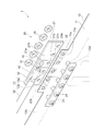
- FIG. 1 is a diagram showing a configuration of a film antenna 1 to which the present embodiment is applied.
- the film antenna 1 to which this embodiment is applied functions as one of flexible printed circuit board structures.
- the film antenna 1 to which this embodiment is applied is connected to an antenna unit 10 which is one of flexible printed boards on which a high-frequency circuit is formed, and a coaxial cable 30 for supplying power to the antenna unit 10.
- the power supply unit 20 is provided.
- an antenna 12 using a transparent conductive material having high light transmission is formed on a film 11 made of a transparent resin material having high light transmission such as PET (Poly Ethylene Terephthalate) resin.
- PET Poly Ethylene Terephthalate
- the antenna 12 includes, for example, a dual frequency shared antenna 12a that shares two frequencies of an 800 MHz band and a 2.1 GHz band, and an antenna GND unit 12b connected to the ground (GND).
- the high-frequency circuit includes a power feeding circuit and a distribution circuit.
- the flexible printed circuit board structure of the present embodiment can be applied to a substrate having these circuits.
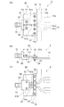
- FIG. 2 is a diagram for explaining the power feeding unit 20 of the film antenna 1 to which the present embodiment is applied.
- the power feeding unit 20 includes a power feeding substrate 21 to which the coaxial cable 30 is connected, and a pressing member 23 that presses the contact 13 of the antenna unit 10 against the power feeding substrate 21.
- the power feeding unit 20 is provided with a male screw (screw) 24 and a female screw (nut) 25.
- the pressing member 23 sandwiches the region having the contact 13 of the antenna unit 10 (the protruding portion 11a formed at one end of the film 11 (upper portion in FIG. 2)) together with the power supply substrate 21 so that the contact 13 and the power supply substrate 21 are sandwiched. Are electrically connected.
- the pressing member 23 is provided with a plurality of through holes, and is pressed using a male screw (screw) 24 and a female screw (nut) 25 to contact the contact 13 of the antenna unit 10 and the power supply board. 21 is electrically connected.
- the contact point 13 is formed on the surface of the protruding portion 11a of the film 11 that faces the power supply substrate 21 (in FIG. 2, the back side of the protruding portion 11a).
- the contact 13 of the antenna unit 10 is provided with an antenna contact 13a that is electrically connected to the dual frequency antenna 12a of the antenna 12 and a GND contact 13b that is electrically connected to the antenna GND 12b of the antenna 12.
- the projecting portion 11 a of the film 11 is provided with a through hole 11 b through which a male screw (screw) 24 passes.
- the through-hole 11b is provided corresponding to each formation location of the antenna contact 13a and the GND contact 13b. In the example shown in FIG.
- the number of through holes 11b is not limited to the above number.
- the size of the antenna contact 13a or the GND contact 13b may be adjusted, and when the antenna contact 13a or the GND contact 13b is small, at least one is necessary, but when the antenna contact 13a or GND contact 13b is large, there may be three or more.
- the power supply board 21 is a glass epoxy board such as FR-4 (Flame Retardant 4) or CEM-3 (Composite Epoxy material 3), and is on the surface facing the contact 13 of the antenna unit 10.
- the pattern is formed of copper.
- the power supply substrate 21 is formed with a power supply substrate antenna power supply portion 21a in the center and a power supply substrate GND portion 21b that is insulated from the power supply substrate antenna power supply portion 21a around the power supply substrate antenna power supply portion 21a. More specifically, the power supply board antenna power supply part 21a faces the antenna contact 13a and the power supply board GND part 21b faces the GND contact 13b below the approximate center of the power supply board 21.
- one through hole 21c is provided in the power supply substrate antenna power supply portion 21a, and four through holes 21c are provided on the power supply substrate GND portion 21b. .
- the through hole 21 c is provided corresponding to the through hole 11 b of the film 11.
- An area for fixing the coaxial cable 30 is secured above the approximate center of the power supply substrate 21.
- the coaxial cable 30 is soldered in a region above the power supply substrate 21. More specifically, the feeding board antenna feeding section 21 a provided at the center on the feeding board 21 and the core wire 31 of the coaxial cable 30 are joined by the solder 41, and the feeding board GND section 21 b on the feeding board 21 and the coaxial cable 30 are connected. The outer conductor 32 is joined by solder 42.
- the coaxial cable 30 is soldered to the power supply board 21 in advance, and then pressed to electrically connect the contact 13 of the antenna unit 10 and the power supply board 21, so that soldering is performed during the soldering process.
- the heat given to the attachment portion is not transmitted to the film 11. Therefore, even when a resin film having a low heat resistance with respect to the film 11 is used, for example, the film 11 is not affected by heat generated during soldering.
- a conductive paste is used as one of the conductive materials on the contact 13 formed on the projecting portion 11a of the film 11 in the antenna portion 10 where the antenna contact 13a and the GND contact 13b are formed.
- a certain silver paste 22 is formed.
- the silver paste 22 is provided on the side where the contact 13 on the side (the back side in FIG. 2) of the protruding portion 11a of the film 11 that faces the power supply substrate 21 is formed.
- the silver paste power distribution unit 22a and the silver paste GND unit The area is divided into 22b and applied.
- the silver paste 22 is applied to the contact 13 by printing, for example. By applying the silver paste 22, the conductivity between the contact 13 and the power supply substrate 21 can be increased.
- the silver paste 22 is used as an example of the intervening conductive material.
- the material is not limited to the silver paste 22, and other materials may be used as long as the conductivity is high and the material is a paste.
- the position of the contact with the silver paste 22 at the contact 13 of the antenna unit 10 is aligned with the contact of the power supply substrate 21. More specifically, the silver paste power distribution unit 22a and the power supply substrate antenna power supply unit 21a of the power supply substrate 21 are combined, the silver paste GND unit 22b and the power supply substrate GND unit 21b of the power supply substrate 21 are combined, and the through hole of the film 11 11b and the through-hole 21c of the electric power feeding board 21 are aligned.
- the pressing member 23 is disposed on the side of the film 11 where the contact 13 is not formed, and the male screw (screw) 24 is inserted into the through hole of the pressing member 23, the through hole 11 b of the film 11, and the through hole 21 c of the power supply substrate 21.
- a female screw (nut) 24 is applied to the side of the power supply substrate 21 where the power supply substrate antenna power supply portion 21a and the power supply substrate GND portion 21b are not formed (the back side in FIG. 2), and the male screw 24 is tightened.
- the contact 13 coated with the silver paste 22 is pressed by the power supply substrate 21 and the pressing member 23, and the antenna contact 13a and the power supply substrate antenna power supply portion 21a, and the GND contact 13b and the power supply substrate GND portion 21b are connected. Connect electrically.
- the 7th-order PIM level appearing in the 800 MHz band is “ ⁇ 82 dBm” before the countermeasure and “ ⁇ 129 dBm” after the countermeasure.
- the distortion component of “47 dB” was improved.
- the 19th-order PIM level appearing in the 2.1 GHz band was “ ⁇ 110 dBm” before the countermeasure and “ ⁇ 135 dBm” after the countermeasure, and the distortion component of “25 dB” was improved.
- the PIM characteristics are improved and a more stable state can be obtained.
- FIGS. 3A to 3C are diagrams showing the configuration of the film antenna 2 to which the second embodiment is applied.
- 3B is a view of the film antenna 2 as viewed from one direction
- FIG. 3A is a view of FIG. 3B from above
- FIG. 3C is a view of FIG. 3B from below. It is a figure.
- the film antenna 2 differs from the film antenna 1 according to the first embodiment in that a connector 70 is connected instead of the coaxial cable 30. Because of this difference, a power feeding unit 60 is provided instead of the power feeding unit 20 of the first embodiment.
- the same functions as those of the first embodiment are denoted by the same reference numerals, and detailed description thereof is omitted here.
- the film antenna 2 to which the second embodiment is applied also functions as one of the flexible printed circuit board structures, and includes a power feeding unit 60 to which a connector 70 for feeding power to the antenna unit 10 is connected. Yes.
- the power feeding section 60 has a power feeding board 61 to which the connector 70 is connected, and presses the contact 13 of the antenna section 10 with the power feeding board 61 and the pressing member 23.
- the power supply section 60 is provided with a male screw (screw) 24 and a female screw (nut) 25.
- the contact point 13 is formed on the surface on the side facing the power supply substrate 61 at the protruding portion 11 a of the film 11.
- the structure of the contact 13 is the same as that of the first embodiment.
- the pressing member 23, male screw (screw) 24, and female screw (nut) 25 are the same as those in the first embodiment.
- the power supply board 61 is formed of, for example, a microstrip line having an impedance of about 50 ⁇ , a transmission line 61d for power supply is provided on the upper surface (front surface), and a conductor is provided on the lower surface (back surface).
- the power supply substrate GND part 61b is formed.
- the power supply substrate GND portion 61b and the power supply substrate antenna power supply portion 61a, which are conductors on the lower surface, are insulated.
- the transmission line 61d on the upper surface of the power supply substrate 61 and the power supply substrate antenna power supply portion 61a on the lower surface are connected via a through hole 61e.
- the power supply substrate antenna power supply portion 61a and the power supply substrate GND portion 61b of the power supply substrate 61 are opposed to the contact 13 of the film 11 at one end of the power supply substrate 61 on the right side of the drawings in FIGS. 3 (a) to 3 (c). Yes.
- the feed board antenna feed section 61a and the feed board GND section 61b facing the contact 13 are provided with through holes 61c corresponding to the through holes (not shown here) of the film 11. More specifically, one through hole 61c is provided in the power supply substrate antenna power supply portion 61a, and two through holes 61c are provided on the left and right sides in the power supply substrate GND portion 61b.
- the connector 70 used for the film antenna 2 for example, a screw-type male connector or the like can be adopted, and a screw portion 72 is provided on one end side thereof, and an external cable (not shown) is connected via the screw portion 72. Connect. The other end of the connector 70 is connected to the conductive plate 80.
- the screw portion 72 and the conductive plate 80 of the connector 70 function as a GND line.
- the conductive plate 80 is composed of a highly conductive material such as copper, for example, and has an L shape in the example shown in FIGS. 3A to 3C.
- the conductive plate 80 is connected to the connector 70 at the vertical start in FIG. 3B, and is connected to the power supply board GND portion 61b of the power supply board 61 in the L-shaped inner horizontal direction.
- the conductive plate 80 and the power supply board GND portion 61b are fixed by screws 81.
- a signal line 71 extends from the connector 70, and the signal line 71 is joined to the transmission line 61 d on the upper surface of the power supply substrate 61 by solder 41.
- the silver paste 22 which is one of the conductive materials is formed on the contact 13 formed on the protruding portion 11a of the film 11 in the antenna unit 10.
- the silver paste 22 is applied to the side where the contact 13 on the side facing the power supply substrate 21 of the protruding portion 11a of the film 11 is formed, for example, by printing.
- the silver paste power distribution unit 22a and the silver paste GND unit 22b described with reference to FIG. 2 are divided into similar structures.
- the power supply substrate 61 and the pressing member 23 are pressed using a male screw (screw) 24 and a female screw (nut) 25, and the contact 13 and the power supply substrate 61 are electrically connected via the silver paste 22. Yes.
- the GND of the conductive plate 80 and the connector 70 is joined according to the structure of the connector 70, for example, by screwing. Further, the signal line 71 of the connector 70 is protruded inside the L-shaped structure of the conductive plate 80 while being insulated from the conductive plate 80. After that, after aligning the conductive plate 80 and the power supply substrate GND portion 61b of the power supply substrate 61, the power supply substrate 61 and the conductive plate 80 are fixed with screws 81, and the power supply substrate GND portion 61b and the conductive plate 80 are electrically connected. Connect to. Further, the signal line 71 of the connector 70 and the transmission line 61 d of the power supply substrate 61 are aligned and soldered, and these are electrically connected by the solder 41.
- a pressing member 23 is disposed on the side of the film 11 where the contact 13 is not formed, and is pressed and fixed by a male screw (screw) 24 and a female screw (nut) 25, and the antenna contact 13a and the power feeding board antenna power supply.
- the portion 61a, the GND contact 13b, and the power supply substrate GND portion 61b are electrically connected.
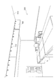
- FIG. 4 is a view showing an embodiment in which the film antenna 1 of the first embodiment or the film antenna 2 of the second embodiment is applied to a vertical smoke barrier 100 as one of indoor partition walls.
- the indoor partition wall in addition to the vertical smoke barrier 100 shown in FIG. 4, for example, it can be applied to a partition partition plate or the like.
- a ceiling installation type antenna or a ceiling embedded type antenna has been used (for example, refer to Japanese Patent Laid-Open No. 9-238812).
- MIMO multiple-input and multiple-output
- An object of the present invention to which the present embodiment is applied is to provide an antenna device that improves the efficiency of installation work without impairing the scenery indoors.
- a vertical smoke barrier 100 is provided in the office 500 for reducing accidents caused by smoke during a fire.
- the vertical smoke barrier 100 is installed with a height vertically downward from the ceiling surface 600 and a length along the ceiling surface 600 so as not to diffuse smoke generated by a fire.
- the antenna is placed at a high place in the room in order to transmit and receive signals throughout the room of the office 500.
- the vertical smoke barrier 100 is provided with an antenna function, it is possible to provide the antenna function together with the function of diffusing smoke and reducing the installation cost without damaging the landscape.
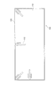
- FIG. 5 is a view for explaining the entire structure of the vertical smoke barrier 100.
- FIG. 6 is a view for explaining a joint portion of the vertical smoke barrier 100.
- the vertical smoke barrier 100 shown in FIG. 5 and FIG. 6 uses a film antenna 110 made of a transparent film made of a resin having a relatively high permeability as a partition material that is formed of a film material or a plate material and partitions an indoor space. Yes.
- An antenna 112 using a transparent conductive material is formed on the film antenna 110.
- the antenna 112 includes, for example, a dual-frequency shared antenna 112a that shares two frequencies of an 800 MHz band and a 2.1 GHz band, and an antenna GND section (not shown) connected to the ground (GND).
- a plurality of (for example, four) antennas 112 are provided, and extend downward from the ceiling surface 600 side as shown in FIG.
- An end 120 is provided around the film antenna 110 as a partition member, and a cover member 121 is provided along the end 120 as shown in FIG.
- An antenna GND part (not shown) is formed on the film antenna 110 in a position hidden by the cover member 121.
- the cover member 121 is formed of a resin material or a metal material, and has a structure in which the cover member 121 and the antenna GND portion are insulated.
- a power supply unit 130 having the same function and structure as the power supply unit 20 or the power supply unit 60 described in detail with reference to FIGS.
- a cable 140 is connected to the power supply unit 130, and the cable 140 and the antenna 112 are electrically connected via the power supply unit 130.
- the wiring structure and the like may be partially different from those of the power feeding unit 20 or the power feeding unit 60, they have substantially the same configuration. That is, the cable 140 and the power supply board (not shown) of the power supply unit 60 are connected by, for example, soldering.
- a conductive material (not shown) made of, for example, silver paste is interposed between the contact point (not shown) of the antenna 112 and the power supply substrate, and is pressed by a pressing member (not shown), The contact point of the antenna 112 and the power supply substrate are electrically connected.
- the other detailed contents are the same as those described with reference to FIGS. 1 to 3, and the description thereof is omitted here.
- FIG. 7 and 8 are diagrams showing other examples of the vertical smoke barrier 100.
- FIG. 7 Although the antenna 112 similar to the vertical smoke barrier 100 shown in FIGS. 5 and 6 is provided, the example shown in FIG. 7 can cope with a plurality of polarized waves, and the example shown in FIG. Then, it is possible to cope with a number of frequency bands. More specifically, in the example shown in FIG. 7, the vertical polarization whose electric field plane is perpendicular to the ground, the horizontal polarization which is horizontal, and the +45 degree polarization whose polarization plane is deviated by 45 degrees in the example shown in FIG. It corresponds to 45 degree polarization. In the example shown in FIG.
Landscapes
- Engineering & Computer Science (AREA)
- Architecture (AREA)
- Physics & Mathematics (AREA)
- Electromagnetism (AREA)
- Civil Engineering (AREA)
- Structural Engineering (AREA)
- Details Of Aerials (AREA)
- Support Of Aerials (AREA)
Abstract
Description
その一方で、近年、異なる2つ以上の周波数で送受信する樹脂製フィルムを用いた可視光透過型アンテナを使用したい、との要求が出てきた。しかしながら、従前の給電構造では好ましいPIM特性を得ることができず、かかる要求に応えることが難しい状況であった。 In a resin film visible light transmissive antenna, which is one of flexible printed boards on which high-frequency circuits are formed, power cannot be supplied by soldering, for example, because the heat resistance of the film is low. Therefore, a power feeding structure that uses a conductive adhesive or conductive double-sided tape for contact is generally adopted for the contact point, but when such a power feeding structure is adopted, the contact point becomes unstable contact, There was deterioration of PIM (Passive Inter Modulation) characteristics.
On the other hand, in recent years, there has been a demand for using a visible light transmission type antenna using a resin film that transmits and receives at two or more different frequencies. However, the conventional power supply structure cannot obtain a preferable PIM characteristic, and it is difficult to meet such a demand.
請求項2に記載の発明は、前記接点と前記給電基板との間に導電性材料を介在させることを特徴とする請求項1記載のフレキシブルプリント基板構造体である。
請求項3に記載の発明は、前記フレキシブルプリント基板は樹脂製フィルムを用いたアンテナであり、前記給電基板は、前記ケーブルまたは前記コネクタが半田付けにより接続されることを特徴とする請求項1または2記載のフレキシブルプリント基板構造体である。
請求項4に記載の発明は、膜材または板材で形成され室内の空間を仕切る仕切材と、前記仕切材の片面または両面に形成され当該仕切材の何れかの端部に接続されるアンテナと、前記仕切材の前記端部に沿って設けられ、前記アンテナに対して給電するためのケーブルまたはコネクタが接続される給電部とを有することを特徴とする室内仕切壁である。
請求項5に記載の発明は、前記給電部は、前記ケーブルまたは前記コネクタが接続される給電基板と、前記アンテナの接点と当該給電基板とを押圧して電気的に接続させる押圧部材と、を有し、当該接点と当該給電基板との間に導電性材料を介在させて電気的に接続させることを特徴とする請求項4記載の室内仕切壁である。 According to the first aspect of the present invention, there is provided a flexible printed circuit board on which a high-frequency circuit is formed, a power supply board to which a cable or a connector for supplying power to the flexible printed circuit board is connected, and a contact point of the flexible printed circuit board. A flexible printed circuit board structure including a pressing member that is sandwiched together with a power supply substrate and presses and electrically connects the contact point and the power supply substrate.
The invention according to
According to a third aspect of the present invention, the flexible printed board is an antenna using a resin film, and the power supply board is connected to the cable or the connector by soldering. 2. The flexible printed circuit board structure according to 2.
The invention according to claim 4 is a partition material that is formed of a film material or a plate material and partitions an indoor space, and an antenna that is formed on one or both surfaces of the partition material and is connected to one end of the partition material. An indoor partition wall comprising: a power supply portion provided along the end portion of the partition member to which a cable or a connector for supplying power to the antenna is connected.
According to a fifth aspect of the present invention, the power feeding unit includes a power feeding board to which the cable or the connector is connected, and a pressing member that presses and electrically connects the contact of the antenna and the power feeding board. 5. The indoor partition wall according to claim 4, wherein the interior partition wall is electrically connected by interposing a conductive material between the contact and the power supply substrate.
請求項2の発明によれば、フレキシブルプリント基板と、ケーブルまたはコネクタとの電気的な接続をさらに安定化させることができる。
請求項3の発明によれば、給電基板に半田付けした場合であっても半田付け工程中に生じる熱が樹脂製フィルムに伝わらず、過熱の問題が生じない。
請求項4の発明によれば、屋内においてアンテナ装置を設置する際に、屋内の景観を損ねることを軽減できる。
請求項5の発明によれば、屋内において、フレキシブルプリント基板と、ケーブルまたはコネクタとの電気的な接続を安定化させたアンテナを提供できる。 According to the first aspect of the present invention, the electrical connection between the flexible printed circuit board and the cable or connector can be stabilized, and the deterioration of the PIM characteristics can be reduced.
According to the invention of
According to the third aspect of the present invention, even when soldering to the power supply substrate, heat generated during the soldering process is not transmitted to the resin film, and the problem of overheating does not occur.
According to invention of Claim 4, when installing an antenna apparatus indoors, it can reduce impairing an indoor landscape.
According to the invention of claim 5, it is possible to provide an antenna in which the electrical connection between the flexible printed circuit board and the cable or connector is stabilized indoors.
以下、添付図面を参照して、本発明の実施形態について詳細に説明する。
図1は、本実施形態が適用されるフィルムアンテナ1の構成を示した図である。
本実施形態が適用されるフィルムアンテナ1は、フレキシブルプリント基板構造体の一つとして機能している。そして、本実施形態が適用されるフィルムアンテナ1は、高周波回路が形成されるフレキシブルプリント基板の一つであるアンテナ部10と、アンテナ部10に対して給電するための同軸ケーブル30が接続される給電部20とを備えている。アンテナ部10では、例えばPET(Poly Ethylene Terephthalate)樹脂などの光透過性の高い透明な樹脂製素材からなるフィルム11に、光透過性の高い透明導電材を使用したアンテナ12が形成されている。アンテナ12は、例えば800MHz帯と2.1GHz帯との2周波を共用する2周波共用アンテナ12aと、グランド(GND)に接続されるアンテナGND部12bとを備えている。なお、高周波回路としては、アンテナの他、給電回路や分配回路があり、本実施形態のフレキシブルプリント基板構造体としては、これらの回路を有する基板にも適用できる。 [First Embodiment]
Hereinafter, embodiments of the present invention will be described in detail with reference to the accompanying drawings.
FIG. 1 is a diagram showing a configuration of a
The
なお、本実施形態では介在する導電性材料の一例として銀ペースト22をあげているが、銀ペースト22に限らず、導電率が高くペースト状の材料であれば他の材料であってもよい。 Further, in the present embodiment, a conductive paste is used as one of the conductive materials on the
In the present embodiment, the
次に、図1に示すフィルムアンテナ1の製造方法について、図2を用いて説明する。
まず、給電基板21の給電基板アンテナ給電部21aに同軸ケーブル30の芯線31を合わせ、給電基板21の給電基板GND部21bに同軸ケーブル30の外導体32を合わせ、半田41、42によって接合し、給電基板21と同軸ケーブル30とを接続する。 [Method for Manufacturing Film Antenna 1]
Next, the manufacturing method of the
First, the
次に、第1の実施形態を採用した際の、相互変調ひずみ(PIM)特性の改善効果について、測定結果を説明する。
ここでは、本実施形態の給電部20を採用しない場合(以下、「対策前」と略す。)と、本実施形態の給電部20を採用した場合(以下、「対策後」と略す。)とで、PIMの測定を行なった。この「対策前」として、接点13のアンテナ接点13aと同軸ケーブル30の芯線31とを導電性接着剤にて接続し、接点13のGND接点13bと同軸ケーブル30の外導体32とを同様に導電性接着剤にて接続している。試作アンテナとしては、800MHz帯と2.1GHz帯との共用アンテナを用いた。
まず、800MHz帯と2.1GHz帯との2波の信号を各1Wで送信したところ、800MHz帯に現われる7次のPIMのレベルが、対策前では「-82dBm」、対策後は「-129dBm」となり、「47dB」の歪成分が改善された。また、2.1GHz帯に現われる19次のPIMのレベルが、対策前では「-110dBm」、対策後は「-135dBm」となり、「25dB」の歪成分が改善された。このように、本実施形態を採用することで、PIM特性が改善され、より安定な状態が得られることが理解できる。 [Improvement effect of PIM characteristics by film antenna 1]
Next, a description will be given of the measurement result of the improvement effect of the intermodulation distortion (PIM) characteristic when the first embodiment is adopted.
Here, when the
First, when signals of 2 waves of 800 MHz band and 2.1 GHz band are transmitted at 1 W each, the 7th-order PIM level appearing in the 800 MHz band is “−82 dBm” before the countermeasure and “−129 dBm” after the countermeasure. Thus, the distortion component of “47 dB” was improved. Also, the 19th-order PIM level appearing in the 2.1 GHz band was “−110 dBm” before the countermeasure and “−135 dBm” after the countermeasure, and the distortion component of “25 dB” was improved. Thus, it can be understood that by adopting this embodiment, the PIM characteristics are improved and a more stable state can be obtained.
図3(a)~(c)は、第2の実施形態が適用されるフィルムアンテナ2の構成を示した図である。図3(b)はフィルムアンテナ2を一方向から眺めた図であり、図3(a)は図3(b)を上方から眺め、図3(c)は図3(b)を下方から眺めた図である。フィルムアンテナ2は第1の実施形態であるフィルムアンテナ1に対し、同軸ケーブル30の代わりにコネクタ70が接続されている点で異なる。かかる相違から、第1の実施形態の給電部20に変えて、給電部60が設けられている。なお、第1の実施形態と同様の機能については同様の符号を用い、ここではその詳細な説明を省略する。 [Second Embodiment]
FIGS. 3A to 3C are diagrams showing the configuration of the
図3(a)~(c)に示すように、給電部60は、コネクタ70が接続される給電基板61を有し、アンテナ部10の接点13を給電基板61と押圧部材23とで押圧する。また、給電部60には、雄ネジ(ビス)24と雌ネジ(ナット)25とが設けられている。接点13は、フィルム11の突出箇所11aにて、給電基板61と対峙する側の面に形成されている。接点13の構造は、第1の実施形態と同様である。また、押圧部材23、雄ネジ(ビス)24および雌ネジ(ナット)25も第1の実施形態と同様である。 The
As shown in FIGS. 3A to 3C, the
次に、図3(a)~(c)に示すフィルムアンテナ2の製造方法について説明する。
まず、導電板80とコネクタ70とのGNDを、例えばネジ込みなど、コネクタ70の構造に応じて接合させる。また、導電板80からは絶縁した状態で、コネクタ70の信号線71を導電板80のL字構造の内側に突出させる。その後、導電板80と給電基板61の給電基板GND部61bとを位置合わせした後、給電基板61と導電板80とをネジ81によって固定し、給電基板GND部61bと導電板80とを電気的に接続させる。また、コネクタ70の信号線71と給電基板61の伝送線路61dとを位置合わせして半田付けを行い、半田41によってこれらを電気的に接続する。 [Method of manufacturing film antenna 2]
Next, a method for manufacturing the
First, the GND of the
次に、本実施形態が適用されるフィルムアンテナの応用例について説明する。
図4は、第1の実施形態のフィルムアンテナ1または第2の実施形態のフィルムアンテナ2を、室内仕切壁の一つとしての垂直防煙壁100に適用する実施形態を示した図である。室内仕切壁としては、図4に示す垂直防煙壁100の他に、例えばパーティションの仕切板などに適用することができる。 [Application as interior partition walls]
Next, an application example of the film antenna to which the present embodiment is applied will be described.
FIG. 4 is a view showing an embodiment in which the
本実施形態が適用される一発明では、屋内において景観を損ねることなく、設置作業の効率化を図るアンテナ装置を提供することを目的としている。 Conventionally, in order to install an antenna in an indoor system, a ceiling installation type antenna or a ceiling embedded type antenna has been used (for example, refer to Japanese Patent Laid-Open No. 9-238812). Here, in a multiple input / multiple output system (MIMO (multiple-input and multiple-output) system) that combines multiple antennas to expand the bandwidth of data transmission / reception, multiple antennas are required. When the ceiling-embedded antenna is used, the landscape is damaged, and there are various problems such as loss of freedom of arrangement and increase in installation cost.
An object of the present invention to which the present embodiment is applied is to provide an antenna device that improves the efficiency of installation work without impairing the scenery indoors.
図5、図6に示す垂直防煙壁100は、膜材または板材で形成され室内の空間を仕切る仕切材として、透過性の比較的高い樹脂製の透明フィルムを用いたフィルムアンテナ110を用いている。フィルムアンテナ110には透明導電材を使用したアンテナ112が形成されている。アンテナ112は、例えば800MHz帯と2.1GHz帯との2周波を共用する2周波共用アンテナ112aと、グランド(GND)に接続されるアンテナGND部(図示せず)とを備えている。図5に示す例では、複数個(例えば4個)のアンテナ112が設けられており、図4に示すように天井面600側から下方に向けて延びている。 FIG. 5 is a view for explaining the entire structure of the
The
Claims (5)
- 高周波回路が形成されるフレキシブルプリント基板と、
前記フレキシブルプリント基板に対して給電するためのケーブルまたはコネクタが接続される給電基板と、
前記フレキシブルプリント基板の接点を前記給電基板とともに挟み込み、当該接点と当該給電基板とを押圧して電気的に接続させる押圧部材と
を有することを特徴とするフレキシブルプリント基板構造体。 A flexible printed circuit board on which a high-frequency circuit is formed;
A power supply board to which a cable or a connector for supplying power to the flexible printed circuit board is connected;
A flexible printed circuit board structure comprising: a pressing member that sandwiches the contact point of the flexible printed circuit board together with the power supply substrate and presses and electrically connects the contact point and the power supply substrate. - 前記接点と前記給電基板との間に導電性材料を介在させることを特徴とする請求項1記載のフレキシブルプリント基板構造体。 2. A flexible printed circuit board structure according to claim 1, wherein a conductive material is interposed between the contact and the power supply substrate.
- 前記フレキシブルプリント基板は樹脂製フィルムを用いたアンテナであり、
前記給電基板は、前記ケーブルまたは前記コネクタが半田付けにより接続されることを特徴とする請求項1または2記載のフレキシブルプリント基板構造体。 The flexible printed board is an antenna using a resin film,
The flexible printed circuit board structure according to claim 1, wherein the power supply board is connected to the cable or the connector by soldering. - 膜材または板材で形成され室内の空間を仕切る仕切材と、
前記仕切材の片面または両面に形成され当該仕切材の何れかの端部に接続されるアンテナと、
前記仕切材の前記端部に沿って設けられ、前記アンテナに対して給電するためのケーブルまたはコネクタが接続される給電部と
を有することを特徴とする室内仕切壁。 A partition material formed of a film material or a plate material and partitioning the indoor space;
An antenna formed on one or both sides of the partition member and connected to either end of the partition member;
An indoor partition wall, comprising: a power supply portion provided along the end portion of the partition material, to which a cable or a connector for supplying power to the antenna is connected. - 前記給電部は、前記ケーブルまたは前記コネクタが接続される給電基板と、前記アンテナの接点と当該給電基板とを押圧して電気的に接続させる押圧部材と、を有し、当該接点と当該給電基板との間に導電性材料を介在させて電気的に接続させることを特徴とする請求項4記載の室内仕切壁。 The power supply unit includes a power supply substrate to which the cable or the connector is connected, and a pressing member that presses and electrically connects the contact of the antenna and the power supply substrate, and the contact and the power supply substrate. The interior partition wall according to claim 4, wherein a conductive material is interposed between and electrically connected to each other.
Priority Applications (4)
| Application Number | Priority Date | Filing Date | Title |
|---|---|---|---|
| CN201780020553.5A CN109075440B (en) | 2016-03-28 | 2017-02-16 | Flexible printed circuit board structure and indoor partition wall |
| US16/088,515 US10487498B2 (en) | 2016-03-28 | 2017-02-16 | Flexible printed circuit board structure and indoor partition wall |
| EP17773796.2A EP3439106B1 (en) | 2016-03-28 | 2017-02-16 | Flexible printed circuit board structure and indoor partition wall |
| KR1020187028188A KR102073505B1 (en) | 2016-03-28 | 2017-02-16 | Flexible Printed Board Structures, and Interior Partition Walls |
Applications Claiming Priority (2)
| Application Number | Priority Date | Filing Date | Title |
|---|---|---|---|
| JP2016064730A JP6317385B2 (en) | 2016-03-28 | 2016-03-28 | Flexible printed circuit board structure and interior partition wall |
| JP2016-064730 | 2016-03-28 |
Publications (1)
| Publication Number | Publication Date |
|---|---|
| WO2017169248A1 true WO2017169248A1 (en) | 2017-10-05 |
Family
ID=59964102
Family Applications (1)
| Application Number | Title | Priority Date | Filing Date |
|---|---|---|---|
| PCT/JP2017/005701 WO2017169248A1 (en) | 2016-03-28 | 2017-02-16 | Flexible printed circuit board structure and indoor partition wall |
Country Status (6)
| Country | Link |
|---|---|
| US (1) | US10487498B2 (en) |
| EP (1) | EP3439106B1 (en) |
| JP (1) | JP6317385B2 (en) |
| KR (1) | KR102073505B1 (en) |
| CN (1) | CN109075440B (en) |
| WO (1) | WO2017169248A1 (en) |
Families Citing this family (4)
| Publication number | Priority date | Publication date | Assignee | Title |
|---|---|---|---|---|
| US10938085B2 (en) | 2017-02-06 | 2021-03-02 | Nihon Dengyo Kosaku Co., Ltd. | Antenna structure |
| CN113193339B (en) * | 2021-03-22 | 2023-01-10 | 安徽精卓光显技术有限责任公司 | Transparent room divides ceiling antenna |
| KR20230032305A (en) * | 2021-08-30 | 2023-03-07 | 주식회사 센서뷰 | Transparent Antenna |
| WO2024061849A1 (en) * | 2022-09-20 | 2024-03-28 | Agc Glass Europe | Apparatus and associated methods and uses |
Citations (8)
| Publication number | Priority date | Publication date | Assignee | Title |
|---|---|---|---|---|
| JPS63254804A (en) * | 1987-04-10 | 1988-10-21 | Yagi Antenna Co Ltd | Antenna feeder |
| JPS6449302A (en) * | 1987-08-19 | 1989-02-23 | Dainippon Printing Co Ltd | Film antenna |
| JPH0455810U (en) * | 1990-09-18 | 1992-05-13 | ||
| JP2006287729A (en) * | 2005-04-01 | 2006-10-19 | Nissha Printing Co Ltd | Transparent antenna for window of building, and translucent member for window of building with antenna |
| JP2008187383A (en) * | 2007-01-29 | 2008-08-14 | Maspro Denkoh Corp | Film antenna, power supply device, and receiving system for traveling object |
| JP2010034924A (en) * | 2008-07-30 | 2010-02-12 | Kojima Press Industry Co Ltd | On-vehicle antenna |
| JP2011091556A (en) * | 2009-10-21 | 2011-05-06 | Panasonic Corp | Antenna device |
| JP2013255094A (en) * | 2012-06-07 | 2013-12-19 | Harada Ind Co Ltd | Antenna power feeding device |
Family Cites Families (23)
| Publication number | Priority date | Publication date | Assignee | Title |
|---|---|---|---|---|
| JPH0611083B2 (en) * | 1987-04-10 | 1994-02-09 | 八木アンテナ株式会社 | Antenna device |
| KR900009111B1 (en) | 1986-11-07 | 1990-12-22 | 야기 안테나 가부시기가이샤 | Antenna devices of film |
| JP3204347B2 (en) | 1993-07-15 | 2001-09-04 | キヤノン株式会社 | Optical element molding equipment |
| JPH0733452U (en) | 1993-11-30 | 1995-06-20 | 愛知製鋼株式会社 | Ladle traveling cart |
| JPH09238012A (en) | 1996-02-29 | 1997-09-09 | Matsushita Electric Works Ltd | Antenna device |
| CN2259642Y (en) * | 1996-04-12 | 1997-08-13 | 鸿海精密工业股份有限公司 | Connector for connecting through storage card connector and main circuit board |
| FR2748862B1 (en) | 1996-05-17 | 1998-07-17 | Radiall Sa | DEVICE FOR CONNECTING A COAXIAL CABLE TO A PRINTED CIRCUIT BOARD |
| JP4350247B2 (en) * | 1999-12-27 | 2009-10-21 | 原田工業株式会社 | Film antenna |
| EP1291970A4 (en) | 2001-02-05 | 2009-08-05 | Sony Corp | Low profile small antenna and constructing method therefor |
| US6548762B2 (en) * | 2001-02-21 | 2003-04-15 | Andrew Corporation | Transmission line grounding lug |
| JP4076931B2 (en) * | 2003-09-02 | 2008-04-16 | 日本アンテナ株式会社 | Antenna feeder |
| US7322833B1 (en) * | 2006-10-31 | 2008-01-29 | Flextronics Ap, Llc | Connection of FPC antenna to PCB |
| JP4281116B2 (en) | 2007-04-27 | 2009-06-17 | 日本電気株式会社 | Power supply device |
| KR100960018B1 (en) * | 2007-11-29 | 2010-05-28 | 한국전자통신연구원 | A Non-Dispersive UWB Antenna Apparatus Using the Multi-Resonance |
| KR101217650B1 (en) * | 2009-07-02 | 2013-01-04 | 주식회사 프로이천 | board connector |
| CN102201613A (en) * | 2010-03-24 | 2011-09-28 | 孙全辉 | Multi-frequency-range ceiling-type antenna |
| JP5555610B2 (en) * | 2010-11-19 | 2014-07-23 | 日本板硝子株式会社 | Terminal, glass plate with terminal and glass plate with terminal for moving body |
| JP5708519B2 (en) * | 2012-02-03 | 2015-04-30 | 株式会社デンソー | Solar cell integrated antenna |
| CN103151605B (en) * | 2012-03-31 | 2015-06-17 | 深圳光启创新技术有限公司 | Wireless fidelity (Wi-Fi) ceiling mounted antenna device |
| JP2013254804A (en) * | 2012-06-06 | 2013-12-19 | Ps4 Luxco S A R L | Semiconductor device and method of manufacturing the same |
| US9742060B2 (en) * | 2014-08-06 | 2017-08-22 | Michael Clyde Walker | Ceiling assembly with integrated repeater antenna |
| US10024883B2 (en) * | 2015-03-27 | 2018-07-17 | Yokowo Co., Ltd. | Contact unit and inspection jig |
| CN204968248U (en) * | 2015-10-09 | 2016-01-13 | 河北工程技术高等专科学校 | Flexible circuit board clamp |
-
2016
- 2016-03-28 JP JP2016064730A patent/JP6317385B2/en active Active
-
2017
- 2017-02-16 KR KR1020187028188A patent/KR102073505B1/en active IP Right Grant
- 2017-02-16 EP EP17773796.2A patent/EP3439106B1/en active Active
- 2017-02-16 CN CN201780020553.5A patent/CN109075440B/en active Active
- 2017-02-16 US US16/088,515 patent/US10487498B2/en active Active
- 2017-02-16 WO PCT/JP2017/005701 patent/WO2017169248A1/en active Application Filing
Patent Citations (8)
| Publication number | Priority date | Publication date | Assignee | Title |
|---|---|---|---|---|
| JPS63254804A (en) * | 1987-04-10 | 1988-10-21 | Yagi Antenna Co Ltd | Antenna feeder |
| JPS6449302A (en) * | 1987-08-19 | 1989-02-23 | Dainippon Printing Co Ltd | Film antenna |
| JPH0455810U (en) * | 1990-09-18 | 1992-05-13 | ||
| JP2006287729A (en) * | 2005-04-01 | 2006-10-19 | Nissha Printing Co Ltd | Transparent antenna for window of building, and translucent member for window of building with antenna |
| JP2008187383A (en) * | 2007-01-29 | 2008-08-14 | Maspro Denkoh Corp | Film antenna, power supply device, and receiving system for traveling object |
| JP2010034924A (en) * | 2008-07-30 | 2010-02-12 | Kojima Press Industry Co Ltd | On-vehicle antenna |
| JP2011091556A (en) * | 2009-10-21 | 2011-05-06 | Panasonic Corp | Antenna device |
| JP2013255094A (en) * | 2012-06-07 | 2013-12-19 | Harada Ind Co Ltd | Antenna power feeding device |
Non-Patent Citations (1)
| Title |
|---|
| See also references of EP3439106A4 * |
Also Published As
| Publication number | Publication date |
|---|---|
| EP3439106A1 (en) | 2019-02-06 |
| EP3439106B1 (en) | 2023-06-07 |
| CN109075440B (en) | 2021-06-01 |
| KR102073505B1 (en) | 2020-02-04 |
| EP3439106A4 (en) | 2019-11-13 |
| CN109075440A (en) | 2018-12-21 |
| EP3439106C0 (en) | 2023-06-07 |
| US10487498B2 (en) | 2019-11-26 |
| US20190112806A1 (en) | 2019-04-18 |
| JP2017183850A (en) | 2017-10-05 |
| JP6317385B2 (en) | 2018-04-25 |
| KR20180116414A (en) | 2018-10-24 |
Similar Documents
| Publication | Publication Date | Title |
|---|---|---|
| WO2017169248A1 (en) | Flexible printed circuit board structure and indoor partition wall | |
| CN101904052B (en) | Patch antenna device | |
| JP7239743B2 (en) | Antenna unit and terminal equipment | |
| JP2006024618A (en) | Wiring board | |
| CN109494489B (en) | Filtering integrated base station antenna | |
| CN112909560B (en) | Liquid crystal antenna and manufacturing method thereof | |
| CN109659694B (en) | Phase-shifting feed device and base station antenna | |
| CN101861050A (en) | Flexible printed circuit board | |
| US20190029112A1 (en) | Printed-circuit cable and manufacture method thereof, connection cable, and electrically adjusted antenna system | |
| US9408306B2 (en) | Antenna array feeding structure having circuit boards connected by at least one solderable pin | |
| CN1250548A (en) | Microstrip distribution array for group antenna and such group antenna | |
| TWI451628B (en) | Electronic equipment with antenna | |
| EP2899802B1 (en) | Anti-lightning combined-stripline-circuit system | |
| KR102109621B1 (en) | Three-Dimensional Broadcasting Antenna | |
| CN109546346B (en) | Double-circular polarization antenna unit with laminated structure | |
| JP7245947B1 (en) | Printed wiring boards and wireless communication terminals | |
| EP4145627A1 (en) | Interactive panel | |
| WO2021090896A1 (en) | Antenna and wireless communication device | |
| CN110165361A (en) | A kind of list cone of radiation paster antenna and electronic equipment | |
| CN1825695B (en) | Gain adjustable antenna | |
| CN117154408A (en) | Millimeter wave antenna assembly and display device | |
| TW201721969A (en) | Antenna device with continuous bending structure and application system using the same | |
| WO2018193682A1 (en) | Radio communication device and board | |
| JP2751303B2 (en) | Antenna feeder | |
| WO2019021807A1 (en) | Antenna module and wireless communication device |
Legal Events
| Date | Code | Title | Description |
|---|---|---|---|
| ENP | Entry into the national phase |
Ref document number: 20187028188 Country of ref document: KR Kind code of ref document: A |
|
| NENP | Non-entry into the national phase |
Ref country code: DE |
|
| WWE | Wipo information: entry into national phase |
Ref document number: 2017773796 Country of ref document: EP |
|
| ENP | Entry into the national phase |
Ref document number: 2017773796 Country of ref document: EP Effective date: 20181029 |
|
| 121 | Ep: the epo has been informed by wipo that ep was designated in this application |
Ref document number: 17773796 Country of ref document: EP Kind code of ref document: A1 |