JP2017183850A - Flexible printed circuit board structure and indoor partition wall - Google Patents
Flexible printed circuit board structure and indoor partition wall Download PDFInfo
- Publication number
- JP2017183850A JP2017183850A JP2016064730A JP2016064730A JP2017183850A JP 2017183850 A JP2017183850 A JP 2017183850A JP 2016064730 A JP2016064730 A JP 2016064730A JP 2016064730 A JP2016064730 A JP 2016064730A JP 2017183850 A JP2017183850 A JP 2017183850A
- Authority
- JP
- Japan
- Prior art keywords
- power supply
- antenna
- contact
- supply substrate
- flexible printed
- Prior art date
- Legal status (The legal status is an assumption and is not a legal conclusion. Google has not performed a legal analysis and makes no representation as to the accuracy of the status listed.)
- Granted
Links
- 238000005192 partition Methods 0.000 title claims description 35
- 239000000758 substrate Substances 0.000 claims abstract description 84
- 238000003825 pressing Methods 0.000 claims abstract description 21
- 239000011347 resin Substances 0.000 claims abstract description 14
- 229920005989 resin Polymers 0.000 claims abstract description 14
- 239000000463 material Substances 0.000 claims description 29
- 239000004020 conductor Substances 0.000 claims description 19
- 238000005476 soldering Methods 0.000 claims description 12
- 238000000638 solvent extraction Methods 0.000 claims 1
- BQCADISMDOOEFD-UHFFFAOYSA-N Silver Chemical compound [Ag] BQCADISMDOOEFD-UHFFFAOYSA-N 0.000 abstract description 21
- 229910052709 silver Inorganic materials 0.000 abstract description 21
- 239000004332 silver Substances 0.000 abstract description 21
- 239000000779 smoke Substances 0.000 description 20
- 230000004888 barrier function Effects 0.000 description 17
- 230000005540 biological transmission Effects 0.000 description 9
- 229910000679 solder Inorganic materials 0.000 description 7
- 230000010287 polarization Effects 0.000 description 5
- 238000010586 diagram Methods 0.000 description 4
- 238000009826 distribution Methods 0.000 description 4
- 238000009434 installation Methods 0.000 description 4
- 238000004519 manufacturing process Methods 0.000 description 4
- 239000000853 adhesive Substances 0.000 description 3
- 230000001070 adhesive effect Effects 0.000 description 3
- 238000000034 method Methods 0.000 description 3
- RYGMFSIKBFXOCR-UHFFFAOYSA-N Copper Chemical compound [Cu] RYGMFSIKBFXOCR-UHFFFAOYSA-N 0.000 description 2
- 239000004593 Epoxy Substances 0.000 description 2
- 229910052802 copper Inorganic materials 0.000 description 2
- 239000010949 copper Substances 0.000 description 2
- 230000006866 deterioration Effects 0.000 description 2
- 230000009977 dual effect Effects 0.000 description 2
- 230000000694 effects Effects 0.000 description 2
- 230000006872 improvement Effects 0.000 description 2
- 229920000139 polyethylene terephthalate Polymers 0.000 description 2
- 239000005020 polyethylene terephthalate Substances 0.000 description 2
- 230000008569 process Effects 0.000 description 2
- -1 Poly Ethylene Terephthalate Polymers 0.000 description 1
- 230000015572 biosynthetic process Effects 0.000 description 1
- 239000002131 composite material Substances 0.000 description 1
- 230000005684 electric field Effects 0.000 description 1
- 239000011521 glass Substances 0.000 description 1
- 238000010030 laminating Methods 0.000 description 1
- 238000005259 measurement Methods 0.000 description 1
- 239000007769 metal material Substances 0.000 description 1
- 238000013021 overheating Methods 0.000 description 1
- 230000035699 permeability Effects 0.000 description 1
Images


Classifications
-
- E—FIXED CONSTRUCTIONS
- E04—BUILDING
- E04B—GENERAL BUILDING CONSTRUCTIONS; WALLS, e.g. PARTITIONS; ROOFS; FLOORS; CEILINGS; INSULATION OR OTHER PROTECTION OF BUILDINGS
- E04B2/00—Walls, e.g. partitions, for buildings; Wall construction with regard to insulation; Connections specially adapted to walls
- E04B2/74—Removable non-load-bearing partitions; Partitions with a free upper edge
-
- H—ELECTRICITY
- H01—ELECTRIC ELEMENTS
- H01Q—ANTENNAS, i.e. RADIO AERIALS
- H01Q1/00—Details of, or arrangements associated with, antennas
- H01Q1/36—Structural form of radiating elements, e.g. cone, spiral, umbrella; Particular materials used therewith
- H01Q1/38—Structural form of radiating elements, e.g. cone, spiral, umbrella; Particular materials used therewith formed by a conductive layer on an insulating support
-
- H—ELECTRICITY
- H01—ELECTRIC ELEMENTS
- H01Q—ANTENNAS, i.e. RADIO AERIALS
- H01Q1/00—Details of, or arrangements associated with, antennas
- H01Q1/12—Supports; Mounting means
- H01Q1/1207—Supports; Mounting means for fastening a rigid aerial element
- H01Q1/1221—Supports; Mounting means for fastening a rigid aerial element onto a wall
-
- H—ELECTRICITY
- H01—ELECTRIC ELEMENTS
- H01Q—ANTENNAS, i.e. RADIO AERIALS
- H01Q1/00—Details of, or arrangements associated with, antennas
- H01Q1/44—Details of, or arrangements associated with, antennas using equipment having another main function to serve additionally as an antenna, e.g. means for giving an antenna an aesthetic aspect
-
- H—ELECTRICITY
- H01—ELECTRIC ELEMENTS
- H01Q—ANTENNAS, i.e. RADIO AERIALS
- H01Q1/00—Details of, or arrangements associated with, antennas
- H01Q1/50—Structural association of antennas with earthing switches, lead-in devices or lightning protectors
-
- E—FIXED CONSTRUCTIONS
- E04—BUILDING
- E04B—GENERAL BUILDING CONSTRUCTIONS; WALLS, e.g. PARTITIONS; ROOFS; FLOORS; CEILINGS; INSULATION OR OTHER PROTECTION OF BUILDINGS
- E04B2/00—Walls, e.g. partitions, for buildings; Wall construction with regard to insulation; Connections specially adapted to walls
- E04B2/74—Removable non-load-bearing partitions; Partitions with a free upper edge
- E04B2002/7488—Details of wiring
Landscapes
- Engineering & Computer Science (AREA)
- Architecture (AREA)
- Physics & Mathematics (AREA)
- Electromagnetism (AREA)
- Civil Engineering (AREA)
- Structural Engineering (AREA)
- Details Of Aerials (AREA)
- Support Of Aerials (AREA)
Abstract
Description
本発明は、フレキシブルプリント基板構造体、および室内仕切壁に関する。 The present invention relates to a flexible printed circuit board structure and an indoor partition wall.
特許文献1では、シート状の平面アンテナにて、一見してもアンテナであることが判らず、かつ、アンテナとしての性能も満足し得る透明アンテナを提供するために、透明乃至は略透明であるシート状基材の面に導電性材料を積層して形成されたアンテナパターンを、孔径400〜500μ、線幅80μ程度の多数の微細透孔によってその開口率を面積比で70〜75%程度に高め、基材の透視性に近い透視性を実現する透明アンテナが提案されている。 In Patent Document 1, a sheet-like planar antenna is transparent or substantially transparent in order to provide a transparent antenna that cannot be seen at first glance and can satisfy the performance as an antenna. An antenna pattern formed by laminating a conductive material on the surface of a sheet-like base material has an aperture ratio of about 70 to 75% in terms of area ratio by a large number of fine through holes having a hole diameter of 400 to 500 μm and a line width of about 80 μm. There has been proposed a transparent antenna that enhances and realizes a transparency close to that of the substrate.
高周波回路が形成されるフレキシブルプリント基板の一つである樹脂製フィルムの可視光透過型アンテナでは、フィルムの耐熱性が低いことから、例えば半田付けによる給電ができなかった。そのために、接触点に導電性接着剤や導電性両面テープを使用し導通をとる給電構造が一般に採用されていたが、このような給電構造を採用した場合、接触点が不安定な接触となり、PIM(Passive Inter Modulation)特性の劣化があった。
その一方で、近年、異なる2つ以上の周波数で送受信する樹脂製フィルムを用いた可視光透過型アンテナを使用したい、との要求が出てきた。しかしながら、従前の給電構造では好ましいPIM特性を得ることができず、かかる要求に応えることが難しい状況であった。
In a resin film visible light transmissive antenna, which is one of flexible printed boards on which high-frequency circuits are formed, power cannot be supplied by soldering, for example, because the heat resistance of the film is low. Therefore, a power feeding structure that uses a conductive adhesive or conductive double-sided tape for contact is generally adopted for the contact point, but when such a power feeding structure is adopted, the contact point becomes unstable contact, There was deterioration of PIM (Passive Inter Modulation) characteristics.
On the other hand, in recent years, there has been a demand for using a visible light transmission type antenna using a resin film that transmits and receives at two or more different frequencies. However, the conventional power supply structure cannot obtain a preferable PIM characteristic, and it is difficult to meet such a demand.
本発明は、例えば樹脂製フィルムの可視光透過型アンテナに代表される、高周波回路が形成されるフレキシブルプリント基板にて、PIM特性を安定化させることを主たる目的とする。 The main object of the present invention is to stabilize PIM characteristics in a flexible printed circuit board on which a high-frequency circuit is formed, for example, a resin film visible light transmission antenna.
請求項1に記載の発明は、高周波回路が形成されるフレキシブルプリント基板と、前記フレキシブルプリント基板に対して給電するためのケーブルまたはコネクタが接続される給電基板と、前記フレキシブルプリント基板の接点を前記給電基板とともに挟み込み、当該接点と当該給電基板とを押圧して電気的に接続させる押圧部材とを有することを特徴とするフレキシブルプリント基板構造体である。
請求項2に記載の発明は、前記接点と前記給電基板との間に導電性材料を介在させることを特徴とする請求項1記載のフレキシブルプリント基板構造体である。
請求項3に記載の発明は、前記フレキシブルプリント基板は樹脂製フィルムを用いたアンテナであり、前記給電基板は、前記ケーブルまたは前記コネクタが半田付けにより接続されることを特徴とする請求項1または2記載のフレキシブルプリント基板構造体である。
請求項4に記載の発明は、膜材または板材で形成され室内の空間を仕切る仕切材と、前記仕切材の片面または両面に形成され当該仕切材の何れかの端部に接続されるアンテナと、前記仕切材の前記端部に沿って設けられ、前記アンテナに対して給電するためのケーブルまたはコネクタが接続される給電部とを有することを特徴とする室内仕切壁である。
請求項5に記載の発明は、前記給電部は、前記ケーブルまたは前記コネクタが接続される給電基板と、前記アンテナの接点と当該給電基板とを押圧して電気的に接続させる押圧部材と、を有し、当該接点と当該給電基板との間に導電性材料を介在させて電気的に接続させることを特徴とする請求項4記載の室内仕切壁である。
According to the first aspect of the present invention, there is provided a flexible printed circuit board on which a high-frequency circuit is formed, a power supply board to which a cable or a connector for supplying power to the flexible printed circuit board is connected, and a contact point of the flexible printed circuit board. A flexible printed circuit board structure including a pressing member that is sandwiched together with a power supply substrate and presses and electrically connects the contact point and the power supply substrate.
The invention according to
According to a third aspect of the present invention, the flexible printed board is an antenna using a resin film, and the power supply board is connected to the cable or the connector by soldering. 2. The flexible printed circuit board structure according to 2.
The invention according to claim 4 is a partition material that is formed of a film material or a plate material and partitions an indoor space, and an antenna that is formed on one or both surfaces of the partition material and is connected to one end of the partition material. An indoor partition wall comprising: a power supply portion provided along the end portion of the partition member to which a cable or a connector for supplying power to the antenna is connected.
According to a fifth aspect of the present invention, the power feeding unit includes a power feeding board to which the cable or the connector is connected, and a pressing member that presses and electrically connects the contact of the antenna and the power feeding board. 5. The indoor partition wall according to claim 4, wherein the interior partition wall is electrically connected by interposing a conductive material between the contact and the power supply substrate.
請求項1の発明によれば、フレキシブルプリント基板と、ケーブルまたはコネクタとの電気的な接続を安定化させることができ、PIM特性の劣化を軽減できる。
請求項2の発明によれば、フレキシブルプリント基板と、ケーブルまたはコネクタとの電気的な接続をさらに安定化させることができる。
請求項3の発明によれば、給電基板に半田付けした場合であっても半田付け工程中に生じる熱が樹脂製フィルムに伝わらず、過熱の問題が生じない。
請求項4の発明によれば、屋内においてアンテナ装置を設置する際に、屋内の景観を損ねることを軽減できる。
請求項5の発明によれば、屋内において、フレキシブルプリント基板と、ケーブルまたはコネクタとの電気的な接続を安定化させたアンテナを提供できる。
According to the first aspect of the present invention, the electrical connection between the flexible printed circuit board and the cable or connector can be stabilized, and the deterioration of the PIM characteristics can be reduced.
According to the invention of
According to the third aspect of the present invention, even when soldering to the power supply substrate, heat generated during the soldering process is not transmitted to the resin film, and the problem of overheating does not occur.
According to invention of Claim 4, when installing an antenna apparatus indoors, it can reduce impairing an indoor landscape.
According to the invention of claim 5, it is possible to provide an antenna in which the electrical connection between the flexible printed circuit board and the cable or connector is stabilized indoors.
〔第1の実施形態〕
以下、添付図面を参照して、本発明の実施形態について詳細に説明する。
図1は、本実施形態が適用されるフィルムアンテナ1の構成を示した図である。
本実施形態が適用されるフィルムアンテナ1は、フレキシブルプリント基板構造体の一つとして機能している。そして、本実施形態が適用されるフィルムアンテナ1は、高周波回路が形成されるフレキシブルプリント基板の一つであるアンテナ部10と、アンテナ部10に対して給電するための同軸ケーブル30が接続される給電部20とを備えている。アンテナ部10では、例えばPET(Poly Ethylene Terephthalate)樹脂などの光透過性の高い透明な樹脂製素材からなるフィルム11に、光透過性の高い透明導電材を使用したアンテナ12が形成されている。アンテナ12は、例えば800MHz帯と2.1GHz帯との2周波を共用する2周波共用アンテナ12aと、グランド(GND)に接続されるアンテナGND部12bとを備えている。なお、高周波回路としては、アンテナの他、給電回路や分配回路があり、本実施形態のフレキシブルプリント基板構造体としては、これらの回路を有する基板にも適用できる。
[First Embodiment]
Hereinafter, embodiments of the present invention will be described in detail with reference to the accompanying drawings.
FIG. 1 is a diagram showing a configuration of a film antenna 1 to which the present embodiment is applied.
The film antenna 1 to which this embodiment is applied functions as one of flexible printed circuit board structures. The film antenna 1 to which this embodiment is applied is connected to an
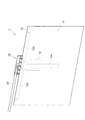
図2は、本実施形態が適用されるフィルムアンテナ1の給電部20を説明するための図である。給電部20は、同軸ケーブル30が接続される給電基板21と、給電基板21にアンテナ部10の接点13を押圧する押圧部材23とを有している。また、給電部20には、雄ネジ(ビス)24と雌ネジ(ナット)25とが設けられている。この押圧部材23は、アンテナ部10の接点13を有する領域(フィルム11の一端部(図2では上部)に形成された突出箇所11a)を給電基板21とともに挟み込み、接点13と給電基板21とを、電気的に接続させている。より詳しくは、押圧部材23には複数個の貫通孔が設けられており、雄ネジ(ビス)24と雌ネジ(ナット)25とを用いて押圧して、アンテナ部10の接点13と給電基板21とを電気的に接続させている。
FIG. 2 is a diagram for explaining the
接点13は、フィルム11の突出箇所11aにて、給電基板21と対峙する側の面(図2では突出箇所11aの裏側)に形成されている。アンテナ部10の接点13には、アンテナ12の2周波共用アンテナ12aと導通しているアンテナ接点13aと、アンテナ12のアンテナGND部12bと導通しているGND接点13bとが設けられている。また、フィルム11の突出箇所11aには、雄ネジ(ビス)24が貫通する貫通孔11bが設けられている。この貫通孔11bは、アンテナ接点13aとGND接点13bとの各々の形成箇所に対応して設けられており、図2に示す例では、アンテナ接点13aに対応する位置に1つ、GND接点13bに対応する位置に4つ(アンテナ接点13aの位置を挟んで左右に2つずつ)が設けられている。なお、貫通孔11bの数は上記の数に限定されるものでは無い。アンテナ接点13aやGND接点13bの大きさに合わせればよく、アンテナ接点13aやGND接点13bが小さい場合には最低でも一つ必要だが、大きい場合には3つ以上あってもよい。
The
給電基板21は、例えば、FR-4(Flame Retardant- 4)やCEM-3(Composite epoxy material-3)などのガラスエポキシ(ガラエポ)素材の基板上であってアンテナ部10の接点13と対峙する面に、例えば銅によってパターンが形成されている。この給電基板21は、中央に給電基板アンテナ給電部21aと、給電基板アンテナ給電部21aの周囲に給電基板アンテナ給電部21aとは絶縁された給電基板GND部21bとが形成されている。より詳しくは、給電基板21の略中央よりも下方側にて、給電基板アンテナ給電部21aがアンテナ接点13aに対峙し、給電基板GND部21bがGND接点13bに対峙している。この給電基板21の略中央よりも下方側には、給電基板アンテナ給電部21aに1つの貫通孔21cと、給電基板GND部21bに左右2つずつの4つの貫通孔21cとが設けられている。貫通孔21cは、フィルム11の貫通孔11bに対応させて設けられている。給電基板21の略中央よりも上方側には、同軸ケーブル30を固定するための領域が確保されている。
The
図2に示すように、給電基板21の上方側の領域にて、同軸ケーブル30が半田付けされている。より詳しくは、給電基板21上の中央に設けられた給電基板アンテナ給電部21aと同軸ケーブル30の芯線31とが半田41によって接合され、給電基板21上の給電基板GND部21bと同軸ケーブル30の外導体32とが半田42によって接合されている。このように給電基板21に対してあらかじめ同軸ケーブル30を半田付けし、その後押圧してアンテナ部10の接点13と給電基板21とを電気的に接続させることで、半田付けを行なう工程中に半田付け部に与えられる熱がフィルム11に伝わることがない。そのため、フィルム11に対して耐熱性の低い例えば樹脂製フィルムを用いた場合であっても、半田付けに際して発生する熱の影響をフィルム11に与えることがない。
As shown in FIG. 2, the
さらに本実施形態では、アンテナ部10におけるフィルム11の突出箇所11aに形成された接点13の、アンテナ接点13aとGND接点13bが形成される箇所に、導電性材料の一つとして、導電性ペーストである銀ペースト22が形成処理されている。銀ペースト22は、フィルム11の突出箇所11aの給電基板21に対峙する側(図2では裏側)の接点13が形成される側に設けられており、銀ペースト配電部22aと、銀ペーストGND部22bとに領域が分かれて塗布されている。銀ペースト22は、例えば印刷により接点13に塗布される。銀ペースト22による塗布が施されることで、接点13と給電基板21との間の導電性を高めることが可能となる。
なお、本実施形態では介在する導電性材料の一例として銀ペースト22をあげているが、銀ペースト22に限らず、導電率が高くペースト状の材料であれば他の材料であってもよい。
Further, in the present embodiment, a conductive paste is used as one of the conductive materials on the
In the present embodiment, the
〔フィルムアンテナ1の製造方法〕
次に、図1に示すフィルムアンテナ1の製造方法について、図2を用いて説明する。
まず、給電基板21の給電基板アンテナ給電部21aに同軸ケーブル30の芯線31を合わせ、給電基板21の給電基板GND部21bに同軸ケーブル30の外導体32を合わせ、半田41、42によって接合し、給電基板21と同軸ケーブル30とを接続する。
[Method for Manufacturing Film Antenna 1]
Next, the manufacturing method of the film antenna 1 shown in FIG. 1 is demonstrated using FIG.
First, the
次に、アンテナ部10の接点13にて銀ペースト22による処理が施された部分と、給電基板21の接点との位置を合わせる。より具体的には、銀ペースト配電部22aと給電基板21の給電基板アンテナ給電部21aとを合わせ、銀ペーストGND部22bと給電基板21の給電基板GND部21bとを合わせ、フィルム11の貫通孔11bと給電基板21の貫通孔21cとの位置を合わせる。
Next, the position of the
その後、フィルム11の接点13が形成されていない側に押圧部材23を配置し、押圧部材23の貫通孔、フィルム11の貫通孔11b、および給電基板21の貫通孔21cに雄ネジ(ビス)24を通す。そして、給電基板21の給電基板アンテナ給電部21aと給電基板GND部21bとが形成されていない側(図2の裏側)から雌ネジ(ナット)25をあてがって雄ネジ(ビス)24を締め付ける。これによって、銀ペースト22が塗布された接点13を、給電基板21と押圧部材23とによって押圧し、アンテナ接点13aと給電基板アンテナ給電部21a、およびGND接点13bと給電基板GND部21bと、を電気的に接続する。
Thereafter, the pressing
〔フィルムアンテナ1によるPIM特性の改善効果〕
次に、第1の実施形態を採用した際の、相互変調ひずみ(PIM)特性の改善効果について、測定結果を説明する。
ここでは、本実施形態の給電部20を採用しない場合(以下、「対策前」と略す。)と、本実施形態の給電部20を採用した場合(以下、「対策後」と略す。)とで、PIMの測定を行なった。この「対策前」として、接点13のアンテナ接点13aと同軸ケーブル30の芯線31とを導電性接着剤にて接続し、接点13のGND接点13bと同軸ケーブル30の外導体32とを同様に導電性接着剤にて接続している。試作アンテナとしては、800MHz帯と2.1GHz帯との共用アンテナを用いた。
まず、800MHz帯と2.1GHz帯との2波の信号を各1Wで送信したところ、800MHz帯に現われる7次のPIMのレベルが、対策前では「−82dBm」、対策後は「−129dBm」となり、「47dB」の歪成分が改善された。また、2.1GHz帯に現われる19次のPIMのレベルが、対策前では「−110dBm」、対策後は「−135dBm」となり、「25dB」の歪成分が改善された。このように、本実施形態を採用することで、PIM特性が改善され、より安定な状態が得られることが理解できる。
[Improvement effect of PIM characteristics by film antenna 1]
Next, a description will be given of the measurement result of the improvement effect of the intermodulation distortion (PIM) characteristic when the first embodiment is adopted.
Here, when the
First, when signals of 2 waves of 800 MHz band and 2.1 GHz band are transmitted at 1 W each, the 7th-order PIM level appearing in the 800 MHz band is “−82 dBm” before the countermeasure, and “−129 dBm” after the countermeasure. Thus, the distortion component of “47 dB” was improved. In addition, the 19th-order PIM level appearing in the 2.1 GHz band was “−110 dBm” before the countermeasure, and “−135 dBm” after the countermeasure, and the distortion component of “25 dB” was improved. Thus, it can be understood that by adopting this embodiment, the PIM characteristics are improved and a more stable state can be obtained.
〔第2の実施形態〕
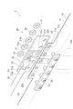
図3(a)〜(c)は、第2の実施形態が適用されるフィルムアンテナ2の構成を示した図である。図3(b)はフィルムアンテナ2を一方向から眺めた図であり、図3(a)は図3(b)を上方から眺め、図3(c)は図3(b)を下方から眺めた図である。フィルムアンテナ2は第1の実施形態であるフィルムアンテナ1に対し、同軸ケーブル30の代わりにコネクタ70が接続されている点で異なる。かかる相違から、第1の実施形態の給電部20に変えて、給電部60が設けられている。なお、第1の実施形態と同様の機能については同様の符号を用い、ここではその詳細な説明を省略する。
[Second Embodiment]
3A to 3C are diagrams showing the configuration of the
第2の実施形態が適用されるフィルムアンテナ2も、フレキシブルプリント基板構造体の一つとして機能しており、アンテナ部10に対して給電するためのコネクタ70が接続される給電部60を備えている。
図3(a)〜(c)に示すように、給電部60は、コネクタ70が接続される給電基板61を有し、アンテナ部10の接点13を給電基板61と押圧部材23とで押圧する。また、給電部60には、雄ネジ(ビス)24と雌ネジ(ナット)25とが設けられている。接点13は、フィルム11の突出箇所11aにて、給電基板61と対峙する側の面に形成されている。接点13の構造は、第1の実施形態と同様である。また、押圧部材23、雄ネジ(ビス)24および雌ネジ(ナット)25も第1の実施形態と同様である。
The
As shown in FIGS. 3A to 3C, the
給電基板61は、例えばインピーダンス50Ω程度のマイクロストリップラインで構成され、上面(表面)に給電のための伝送線路61dが設けられ、下面(裏面)に導体が設けられて給電基板アンテナ給電部61aと給電基板GND部61bとを形成している。この下面の導体である給電基板GND部61bと給電基板アンテナ給電部61aとは、絶縁されている。給電基板61の上面にある伝送線路61dと下面にある給電基板アンテナ給電部61aとは、スルーホール61eを介して接続されている。
The
給電基板61の給電基板アンテナ給電部61aおよび給電基板GND部61bは、図3(a)〜(c)の図示の右側である給電基板61の一端にて、フィルム11の接点13と対峙している。そして、この接点13と対峙する給電基板アンテナ給電部61aおよび給電基板GND部61bには、貫通孔61cがフィルム11の貫通孔(ここでは図示せず)に対応させて設けられている。より詳しくは、給電基板アンテナ給電部61aに1つの貫通孔61cと、給電基板GND部61bに左右2つずつの貫通孔61cとが設けられている。
The power supply board antenna
フィルムアンテナ2に用いられるコネクタ70としては、例えばネジ式のオスコネクタなどを採用することができ、その一端側にネジ部72を有し、外部ケーブル(図示せず)とはネジ部72を介して接続する。また、コネクタ70の他端は、導電板80に接続されている。コネクタ70のネジ部72および導電板80は、GNDラインとして機能している。導電板80は、導通をとる表面や全体が例えば銅などの導電性の高い材料で構成され、図3(a)〜(c)に示す例では、L字型を有している。そして、導電板80は、図3(b)の鉛直方向の立ち上がりでコネクタ70と接続され、L字の内側水平方向にて、給電基板61の給電基板GND部61bに接続されている。導電板80と給電基板GND部61bとは、ネジ81によって固定されている。
As the
コネクタ70からは信号線71が出ており、この信号線71は、給電基板61の上面にある伝送線路61dに対して半田41によって接合されている。給電基板61に対して半田付けによる給電を行った後にアンテナ部10を組み付けることで、フィルム11に対して耐熱性の低い例えば樹脂製フィルムを用いた場合であっても、半田付けに際して発生する熱の影響をフィルム11に与えることがない。
A
さらに本実施形態では、アンテナ部10におけるフィルム11の突出箇所11aに形成された接点13に、導電性材料の一つである銀ペースト22が形成処理されている。銀ペースト22は、フィルム11の突出箇所11aの給電基板21に対峙する側の接点13が形成される側に、例えば印刷により塗布されている。図3(a)〜(c)では記載を省略しているが、図2を用いて説明した銀ペースト配電部22aと銀ペーストGND部22bと、それぞれ同様な構造に領域が分かれている。給電基板61と押圧部材23とを、雄ネジ(ビス)24と雌ネジ(ナット)25とを用いて押圧し、接点13と給電基板61とを銀ペースト22を介して電気的に接続している。
Furthermore, in this embodiment, the
〔フィルムアンテナ2の製造方法〕
次に、図3(a)〜(c)に示すフィルムアンテナ2の製造方法について説明する。
まず、導電板80とコネクタ70とのGNDを、例えばネジ込みなど、コネクタ70の構造に応じて接合させる。また、導電板80からは絶縁した状態で、コネクタ70の信号線71を導電板80のL字構造の内側に突出させる。その後、導電板80と給電基板61の給電基板GND部61bとを位置合わせした後、給電基板61と導電板80とをネジ81によって固定し、給電基板GND部61bと導電板80とを電気的に接続させる。また、コネクタ70の信号線71と給電基板61の伝送線路61dとを位置合わせして半田付けを行い、半田41によってこれらを電気的に接続する。
[Method of manufacturing film antenna 2]
Next, the manufacturing method of the
First, the GND of the
次いで、アンテナ部10の接点13にて銀ペースト22による処理が施された部分と、給電基板61の接点と、の位置を合わせる。その後、フィルム11の接点13が形成されていない側に押圧部材23を配置し、雄ネジ(ビス)24と雌ネジ(ナット)25とによって押圧して固定し、アンテナ接点13aと給電基板アンテナ給電部61a、およびGND接点13bと給電基板GND部61bと、を電気的に接続する。
Next, the position of the portion subjected to the processing with the
〔室内仕切壁としての応用〕
次に、本実施形態が適用されるフィルムアンテナの応用例について説明する。
図4は、第1の実施形態のフィルムアンテナ1または第2の実施形態のフィルムアンテナ2を、室内仕切壁の一つとしての垂直防煙壁100に適用する実施形態を示した図である。室内仕切壁としては、図4に示す垂直防煙壁100の他に、例えばパーティションの仕切板などに適用することができる。
[Application as interior partition walls]
Next, an application example of the film antenna to which the present embodiment is applied will be described.
FIG. 4 is a view showing an embodiment in which the film antenna 1 of the first embodiment or the
従前では、屋内系においてアンテナを設置するには、天井設置型や天井埋込み型のアンテナが用いられていた(例えば、特開平9−238012号公報参照)。ここで、複数のアンテナを組み合わせてデータ送受信の帯域を広げる複数入力・複数出力システム(MIMO(multiple-input and multiple-output)システム)では、複数個のアンテナが必要となり、従前の天井設置型や天井埋め込み型のアンテナを使用すると、景観を損ねてしまい、配置の自由度が無くなってしまったり、設置コストが高騰化してしまったりするなど、種々の問題を生じていた。
本実施形態が適用される一発明では、屋内において景観を損ねることなく、設置作業の効率化を図るアンテナ装置を提供することを目的としている。
Conventionally, in order to install an antenna in an indoor system, a ceiling-mounted antenna or a ceiling-embedded antenna has been used (see, for example, JP-A-9-238812). Here, in a multiple input / multiple output system (MIMO (multiple-input and multiple-output) system) that combines multiple antennas to expand the bandwidth of data transmission / reception, multiple antennas are required. When the ceiling-embedded antenna is used, the landscape is damaged, and there are various problems such as loss of freedom of arrangement and increase in installation cost.
An object of the present invention to which the present embodiment is applied is to provide an antenna device that improves the efficiency of installation work without impairing the scenery indoors.
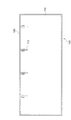
図4に示す実施形態では、オフィス500内に、火災の際の煙による事故を軽減するための垂直防煙壁100が設けられている。一般に、垂直防煙壁100は、火災で発生する煙を拡散させないために、天井面600から鉛直下方に向けた高さと天井面600に沿った長さとを有して設置される。その一方で、一般に、アンテナの設置環境としては、オフィス500の室内全体にて信号の送受を行なうために室内の高所に置かれることが好ましい。本実施形態によれば、垂直防煙壁100にアンテナ機能を備えさせていることから、煙拡散の機能とともに、景観を損ねず設置コストを低減させてアンテナ機能を提供できる。
In the embodiment shown in FIG. 4, a
図5は、垂直防煙壁100の全体構造を説明するための図である。また図6は、垂直防煙壁100の接合部を説明するための図である。
図5、図6に示す垂直防煙壁100は、膜材または板材で形成され室内の空間を仕切る仕切材として、透過性の比較的高い樹脂製の透明フィルムを用いたフィルムアンテナ110を用いている。フィルムアンテナ110には透明導電材を使用したアンテナ112が形成されている。アンテナ112は、例えば800MHz帯と2.1GHz帯との2周波を共用する2周波共用アンテナ112aと、グランド(GND)に接続されるアンテナGND部(図示せず)とを備えている。図5に示す例では、複数個(例えば4個)のアンテナ112が設けられており、図4に示すように天井面600側から下方に向けて延びている。
FIG. 5 is a view for explaining the entire structure of the
The
仕切材であるフィルムアンテナ110の周囲に端部120があり、図6に示すように、この端部120に沿ってカバー部材121が設けられている。アンテナGND部(図示せず)は、このカバー部材121に隠れる位置にあるフィルムアンテナ110に形成されている。カバー部材121は樹脂材または金属材で形成されるが、カバー部材121とアンテナGND部とは絶縁された構造となっている。
An
カバー部材121の内部には、図1〜図3にて詳述した給電部20または給電部60と同様な機能、構造を有する給電部130が設けられている。給電部130にはケーブル140が接続され、給電部130を介してケーブル140とアンテナ112とが電気的に接続される。配線構造などは給電部20または給電部60と一部、異なる場合があるが、ほぼ同様な構成を有している。すなわち、ケーブル140と給電部60の給電基板(図示せず)とは、例えば半田付けにより接続されている。また、アンテナ112の接点(図示せず)と給電基板との間に、例えば銀ペーストなどからなる導電性材料(図示せず)を介在させて、押圧部材(図示せず)にて押圧し、アンテナ112の接点と給電基板とが電気的に接続される。その他の詳細な内容は、図1〜図3にて説明したものと同等であり、ここではその説明を省略する。
Inside the
図7および図8は、垂直防煙壁100の他の例を示した図である。図5、図6に示す垂直防煙壁100と同様なアンテナ112が設けられているが、図7に示す例では複数の偏波に対して対応可能とするものであり、図8に示す例では更に数多くの周波数の帯域に対して対応可能とするものである。より詳しくは、図7に示す例では、偏波のうち電界面が地面に対して垂直である垂直偏波、水平である水平偏波、および偏波面が45度ずれた+45度偏波、−45度偏波、に対応している。また、図8に示す例では、例えば、700MHz帯、800MHz帯、1.5GHz帯、1.7GHz帯、2GHz帯、2.6GHz帯、3.5GHz帯、などの複数の帯域に対して対応可能としている。一般に、垂直防煙壁100は、室内における建造物として、その表面積は比較的広いことから、図7および図8に示すような応用が可能となる。
7 and 8 are diagrams showing another example of the
1…フィルムアンテナ、2…フィルムアンテナ、10…アンテナ部、11…フィルム、12…アンテナ、13…接点、20…給電部、21…給電基板、22…銀ペースト、23…押圧部材、24…雄ネジ(ビス)、25…雌ネジ(ナット)、30…同軸ケーブル、31…芯線、32…外導体、41…半田、42…半田、60…給電部、61…給電基板、70…コネクタ、71…信号線、80…導電板、81…ネジ、100…垂直防煙壁、110…フィルムアンテナ、112…アンテナ、120…端部、130…給電部、140…ケーブル DESCRIPTION OF SYMBOLS 1 ... Film antenna, 2 ... Film antenna, 10 ... Antenna part, 11 ... Film, 12 ... Antenna, 13 ... Contact, 20 ... Feeding part, 21 ... Feeding board, 22 ... Silver paste, 23 ... Pressing member, 24 ... Male Screw (screw), 25 ... Female screw (nut), 30 ... Coaxial cable, 31 ... Core wire, 32 ... Outer conductor, 41 ... Solder, 42 ... Solder, 60 ... Feeding part, 61 ... Feeding board, 70 ... Connector, 71 ... Signal line, 80 ... Conductive plate, 81 ... Screw, 100 ... Vertical smoke barrier, 110 ... Film antenna, 112 ... Antenna, 120 ... End, 130 ... Feeding part, 140 ... Cable
請求項1に記載の発明は、高周波回路が形成されるフレキシブルプリント基板と、前記フレキシブルプリント基板に対して給電するためのケーブルまたはコネクタが接続される給電基板と、前記フレキシブルプリント基板の接点を前記給電基板とともに挟み込み、当該接点と当該給電基板とを押圧して電気的に接続させる押圧部材とを有し、前記フレキシブルプリント基板の前記接点に貫通孔が形成され、前記押圧部材は、前記貫通孔を用いて前記接点と前記給電基板とを押圧することを特徴とするフレキシブルプリント基板構造体である。
請求項2に記載の発明は、他の部分に対して突出する突出箇所を持ち高周波回路が形成されるフレキシブルプリント基板と、前記フレキシブルプリント基板に対して給電するためのケーブルまたはコネクタが接続される給電基板と、前記フレキシブルプリント基板の前記突出箇所に設けた接点を前記給電基板とともに挟み込み、当該接点と当該給電基板とを押圧して電気的に接続させる押圧部材とを有することを特徴とするフレキシブルプリント基板構造体である。
請求項3に記載の発明は、前記接点と前記給電基板との間に導電性材を介在させ、前記フレキシブルプリント基板は樹脂製フィルムを用いたアンテナであり、前記給電基板は、前記ケーブルまたは前記コネクタが半田付けにより接続されることを特徴とする請求項1または2記載のフレキシブルプリント基板構造体である。
請求項4に記載の発明は、膜材または板材で形成され室内の空間を仕切る仕切材と、前記仕切材の片面または両面に形成され当該仕切材の何れかの端部に接続されるアンテナと、前記仕切材の前記端部に沿って設けられ、前記アンテナに対して給電するためのケーブルまたはコネクタが接続される給電部とを有し、前記給電部は、前記ケーブルまたは前記コネクタが接続される給電基板と、前記アンテナの接点と当該給電基板とを押圧して電気的に接続させる押圧部材と、を有し、前記アンテナの前記接点に貫通孔が形成され、前記押圧部材は、前記貫通孔を用いて前記接点を前記給電基板とともに挟み込み、当該接点と当該給電基板とを押圧することを特徴とする室内仕切壁である。
請求項5に記載の発明は、他の部分に対して突出する突出箇所を持ち、膜材または板材で形成され室内の空間を仕切る仕切材と、前記仕切材の片面または両面に形成され当該仕切材の前記突出箇所に接続されるアンテナと、前記仕切材の前記突出箇所に沿って設けられ、前記アンテナに対して給電するためのケーブルまたはコネクタが接続される給電部と
を有することを特徴とする室内仕切壁である。
According to the first aspect of the present invention, there is provided a flexible printed circuit board on which a high-frequency circuit is formed, a power supply board to which a cable or a connector for supplying power to the flexible printed circuit board is connected, and a contact point of the flexible printed circuit board. pinching together the feed substrate, it possesses a pressing member that electrically connects to press the said contact and said power supply board, the through hole in the contact of the flexible printed circuit board is formed, the pressing member, the through hole The flexible printed circuit board structure is characterized in that the contact point and the power supply substrate are pressed by using .
According to the second aspect of the present invention, a flexible printed circuit board having a protruding portion that protrudes from another part and having a high frequency circuit formed thereon, and a cable or connector for supplying power to the flexible printed circuit board are connected. A flexible device comprising: a power supply substrate; and a pressing member that sandwiches a contact provided at the protruding portion of the flexible printed circuit board together with the power supply substrate and presses the contact and the power supply substrate to electrically connect them. It is a printed circuit board structure .
According to a third aspect of the present invention , a conductive material is interposed between the contact point and the power supply board, the flexible printed board is an antenna using a resin film, and the power supply board includes the cable or the power supply board. 3. The flexible printed circuit board structure according to claim 1, wherein the connector is connected by soldering.
The invention according to claim 4 is a partition material that is formed of a film material or a plate material and partitions an indoor space, and an antenna that is formed on one or both surfaces of the partition material and is connected to one end of the partition material. the provided along the end portion of the partition member, have a power feeding portion cable or connector for supplying power to the antenna is connected, the power supply unit, the cable or the connector is connected And a pressing member that presses and electrically connects the contact point of the antenna and the power supply substrate, and a through hole is formed in the contact point of the antenna. An indoor partition wall characterized in that the contact is sandwiched together with the power supply substrate using a hole, and the contact and the power supply substrate are pressed .
The invention according to claim 5 has a projecting portion projecting with respect to the other part, is formed of a film material or a plate material and partitions an indoor space, and is formed on one or both surfaces of the partition material. An antenna connected to the projecting portion of the material, and a power feeding portion provided along the projecting portion of the partition material, to which a cable or a connector for feeding power to the antenna is connected
It is an indoor partition wall characterized by having .
Claims (5)
前記フレキシブルプリント基板に対して給電するためのケーブルまたはコネクタが接続される給電基板と、
前記フレキシブルプリント基板の接点を前記給電基板とともに挟み込み、当該接点と当該給電基板とを押圧して電気的に接続させる押圧部材と
を有することを特徴とするフレキシブルプリント基板構造体。 A flexible printed circuit board on which a high-frequency circuit is formed;
A power supply board to which a cable or a connector for supplying power to the flexible printed circuit board is connected;
A flexible printed circuit board structure comprising: a pressing member that sandwiches the contact point of the flexible printed circuit board together with the power supply substrate and presses and electrically connects the contact point and the power supply substrate.
前記給電基板は、前記ケーブルまたは前記コネクタが半田付けにより接続されることを特徴とする請求項1または2記載のフレキシブルプリント基板構造体。 The flexible printed board is an antenna using a resin film,
The flexible printed circuit board structure according to claim 1, wherein the power supply board is connected to the cable or the connector by soldering.
前記仕切材の片面または両面に形成され当該仕切材の何れかの端部に接続されるアンテナと、
前記仕切材の前記端部に沿って設けられ、前記アンテナに対して給電するためのケーブルまたはコネクタが接続される給電部と
を有することを特徴とする室内仕切壁。 A partition material formed of a film material or a plate material and partitioning the indoor space;
An antenna formed on one or both sides of the partition member and connected to either end of the partition member;
An indoor partition wall, comprising: a power supply portion provided along the end portion of the partition material, to which a cable or a connector for supplying power to the antenna is connected.
Priority Applications (6)
| Application Number | Priority Date | Filing Date | Title |
|---|---|---|---|
| JP2016064730A JP6317385B2 (en) | 2016-03-28 | 2016-03-28 | Flexible printed circuit board structure and interior partition wall |
| PCT/JP2017/005701 WO2017169248A1 (en) | 2016-03-28 | 2017-02-16 | Flexible printed circuit board structure and indoor partition wall |
| US16/088,515 US10487498B2 (en) | 2016-03-28 | 2017-02-16 | Flexible printed circuit board structure and indoor partition wall |
| KR1020187028188A KR102073505B1 (en) | 2016-03-28 | 2017-02-16 | Flexible Printed Board Structures, and Interior Partition Walls |
| CN201780020553.5A CN109075440B (en) | 2016-03-28 | 2017-02-16 | Flexible printed circuit board structure and indoor partition wall |
| EP17773796.2A EP3439106B1 (en) | 2016-03-28 | 2017-02-16 | Flexible printed circuit board structure and indoor partition wall |
Applications Claiming Priority (1)
| Application Number | Priority Date | Filing Date | Title |
|---|---|---|---|
| JP2016064730A JP6317385B2 (en) | 2016-03-28 | 2016-03-28 | Flexible printed circuit board structure and interior partition wall |
Publications (2)
| Publication Number | Publication Date |
|---|---|
| JP2017183850A true JP2017183850A (en) | 2017-10-05 |
| JP6317385B2 JP6317385B2 (en) | 2018-04-25 |
Family
ID=59964102
Family Applications (1)
| Application Number | Title | Priority Date | Filing Date |
|---|---|---|---|
| JP2016064730A Active JP6317385B2 (en) | 2016-03-28 | 2016-03-28 | Flexible printed circuit board structure and interior partition wall |
Country Status (6)
| Country | Link |
|---|---|
| US (1) | US10487498B2 (en) |
| EP (1) | EP3439106B1 (en) |
| JP (1) | JP6317385B2 (en) |
| KR (1) | KR102073505B1 (en) |
| CN (1) | CN109075440B (en) |
| WO (1) | WO2017169248A1 (en) |
Cited By (1)
| Publication number | Priority date | Publication date | Assignee | Title |
|---|---|---|---|---|
| US10938085B2 (en) | 2017-02-06 | 2021-03-02 | Nihon Dengyo Kosaku Co., Ltd. | Antenna structure |
Families Citing this family (3)
| Publication number | Priority date | Publication date | Assignee | Title |
|---|---|---|---|---|
| CN113193339B (en) * | 2021-03-22 | 2023-01-10 | 安徽精卓光显技术有限责任公司 | Transparent room divides ceiling antenna |
| KR20230032305A (en) * | 2021-08-30 | 2023-03-07 | 주식회사 센서뷰 | Transparent Antenna |
| WO2024061849A1 (en) * | 2022-09-20 | 2024-03-28 | Agc Glass Europe | Apparatus and associated methods and uses |
Citations (8)
| Publication number | Priority date | Publication date | Assignee | Title |
|---|---|---|---|---|
| JPS63254804A (en) * | 1987-04-10 | 1988-10-21 | Yagi Antenna Co Ltd | Antenna feeder |
| JPS6449302A (en) * | 1987-08-19 | 1989-02-23 | Dainippon Printing Co Ltd | Film antenna |
| JP2005080074A (en) * | 2003-09-02 | 2005-03-24 | Nippon Antenna Co Ltd | Antenna power supply unit |
| JP2006287729A (en) * | 2005-04-01 | 2006-10-19 | Nissha Printing Co Ltd | Transparent antenna for window of building, and translucent member for window of building with antenna |
| JP2008187383A (en) * | 2007-01-29 | 2008-08-14 | Maspro Denkoh Corp | Film antenna, power supply device, and receiving system for traveling object |
| JP2010034924A (en) * | 2008-07-30 | 2010-02-12 | Kojima Press Industry Co Ltd | On-vehicle antenna |
| JP2011091556A (en) * | 2009-10-21 | 2011-05-06 | Panasonic Corp | Antenna device |
| JP2012113840A (en) * | 2010-11-19 | 2012-06-14 | Nippon Sheet Glass Co Ltd | Terminal, glass plate with terminal, and glass plate with terminal for moving body |
Family Cites Families (23)
| Publication number | Priority date | Publication date | Assignee | Title |
|---|---|---|---|---|
| JPH0611083B2 (en) * | 1987-04-10 | 1994-02-09 | 八木アンテナ株式会社 | Antenna device |
| KR900009111B1 (en) | 1986-11-07 | 1990-12-22 | 야기 안테나 가부시기가이샤 | Antenna devices of film |
| JPH0810970Y2 (en) * | 1990-09-18 | 1996-03-29 | 日本板硝子株式会社 | Connection structure between sheet antenna and feeder line |
| JP3204347B2 (en) | 1993-07-15 | 2001-09-04 | キヤノン株式会社 | Optical element molding equipment |
| JPH0733452U (en) | 1993-11-30 | 1995-06-20 | 愛知製鋼株式会社 | Ladle traveling cart |
| JPH09238012A (en) | 1996-02-29 | 1997-09-09 | Matsushita Electric Works Ltd | Antenna device |
| CN2259642Y (en) * | 1996-04-12 | 1997-08-13 | 鸿海精密工业股份有限公司 | Connector for connecting through storage card connector and main circuit board |
| FR2748862B1 (en) * | 1996-05-17 | 1998-07-17 | Radiall Sa | DEVICE FOR CONNECTING A COAXIAL CABLE TO A PRINTED CIRCUIT BOARD |
| JP4350247B2 (en) * | 1999-12-27 | 2009-10-21 | 原田工業株式会社 | Film antenna |
| US6798383B2 (en) * | 2001-02-05 | 2004-09-28 | Sony Corporation | Low profile small antenna and constructing method therefor |
| US6548762B2 (en) * | 2001-02-21 | 2003-04-15 | Andrew Corporation | Transmission line grounding lug |
| US7322833B1 (en) * | 2006-10-31 | 2008-01-29 | Flextronics Ap, Llc | Connection of FPC antenna to PCB |
| JP4281116B2 (en) * | 2007-04-27 | 2009-06-17 | 日本電気株式会社 | Power supply device |
| KR100960018B1 (en) * | 2007-11-29 | 2010-05-28 | 한국전자통신연구원 | A Non-Dispersive UWB Antenna Apparatus Using the Multi-Resonance |
| KR101217650B1 (en) * | 2009-07-02 | 2013-01-04 | 주식회사 프로이천 | board connector |
| CN102201613A (en) * | 2010-03-24 | 2011-09-28 | 孙全辉 | Multi-frequency-range ceiling-type antenna |
| JP5708519B2 (en) * | 2012-02-03 | 2015-04-30 | 株式会社デンソー | Solar cell integrated antenna |
| CN103151605B (en) * | 2012-03-31 | 2015-06-17 | 深圳光启创新技术有限公司 | Wireless fidelity (Wi-Fi) ceiling mounted antenna device |
| JP2013254804A (en) * | 2012-06-06 | 2013-12-19 | Ps4 Luxco S A R L | Semiconductor device and method of manufacturing the same |
| JP5514262B2 (en) * | 2012-06-07 | 2014-06-04 | 原田工業株式会社 | Antenna feeder |
| US9742060B2 (en) * | 2014-08-06 | 2017-08-22 | Michael Clyde Walker | Ceiling assembly with integrated repeater antenna |
| US10024883B2 (en) * | 2015-03-27 | 2018-07-17 | Yokowo Co., Ltd. | Contact unit and inspection jig |
| CN204968248U (en) * | 2015-10-09 | 2016-01-13 | 河北工程技术高等专科学校 | Flexible circuit board clamp |
-
2016
- 2016-03-28 JP JP2016064730A patent/JP6317385B2/en active Active
-
2017
- 2017-02-16 US US16/088,515 patent/US10487498B2/en active Active
- 2017-02-16 EP EP17773796.2A patent/EP3439106B1/en active Active
- 2017-02-16 WO PCT/JP2017/005701 patent/WO2017169248A1/en active Application Filing
- 2017-02-16 KR KR1020187028188A patent/KR102073505B1/en active IP Right Grant
- 2017-02-16 CN CN201780020553.5A patent/CN109075440B/en active Active
Patent Citations (8)
| Publication number | Priority date | Publication date | Assignee | Title |
|---|---|---|---|---|
| JPS63254804A (en) * | 1987-04-10 | 1988-10-21 | Yagi Antenna Co Ltd | Antenna feeder |
| JPS6449302A (en) * | 1987-08-19 | 1989-02-23 | Dainippon Printing Co Ltd | Film antenna |
| JP2005080074A (en) * | 2003-09-02 | 2005-03-24 | Nippon Antenna Co Ltd | Antenna power supply unit |
| JP2006287729A (en) * | 2005-04-01 | 2006-10-19 | Nissha Printing Co Ltd | Transparent antenna for window of building, and translucent member for window of building with antenna |
| JP2008187383A (en) * | 2007-01-29 | 2008-08-14 | Maspro Denkoh Corp | Film antenna, power supply device, and receiving system for traveling object |
| JP2010034924A (en) * | 2008-07-30 | 2010-02-12 | Kojima Press Industry Co Ltd | On-vehicle antenna |
| JP2011091556A (en) * | 2009-10-21 | 2011-05-06 | Panasonic Corp | Antenna device |
| JP2012113840A (en) * | 2010-11-19 | 2012-06-14 | Nippon Sheet Glass Co Ltd | Terminal, glass plate with terminal, and glass plate with terminal for moving body |
Cited By (1)
| Publication number | Priority date | Publication date | Assignee | Title |
|---|---|---|---|---|
| US10938085B2 (en) | 2017-02-06 | 2021-03-02 | Nihon Dengyo Kosaku Co., Ltd. | Antenna structure |
Also Published As
| Publication number | Publication date |
|---|---|
| US20190112806A1 (en) | 2019-04-18 |
| EP3439106C0 (en) | 2023-06-07 |
| CN109075440A (en) | 2018-12-21 |
| US10487498B2 (en) | 2019-11-26 |
| KR20180116414A (en) | 2018-10-24 |
| WO2017169248A1 (en) | 2017-10-05 |
| EP3439106B1 (en) | 2023-06-07 |
| EP3439106A4 (en) | 2019-11-13 |
| KR102073505B1 (en) | 2020-02-04 |
| JP6317385B2 (en) | 2018-04-25 |
| EP3439106A1 (en) | 2019-02-06 |
| CN109075440B (en) | 2021-06-01 |
Similar Documents
| Publication | Publication Date | Title |
|---|---|---|
| JP6317385B2 (en) | Flexible printed circuit board structure and interior partition wall | |
| JP7239743B2 (en) | Antenna unit and terminal equipment | |
| US20140102763A1 (en) | Rigid flexible circuit board with impedance control | |
| US20100044077A1 (en) | Flat cable | |
| JP2006024618A (en) | Wiring board | |
| CN109494489B (en) | Filtering integrated base station antenna | |
| US20140375513A1 (en) | Antenna device and display apparatus having the same | |
| WO2020155723A1 (en) | Phase shift feed apparatus and base station antenna | |
| JP2023510169A (en) | Antenna assembly and electronics | |
| US20190029112A1 (en) | Printed-circuit cable and manufacture method thereof, connection cable, and electrically adjusted antenna system | |
| US9408306B2 (en) | Antenna array feeding structure having circuit boards connected by at least one solderable pin | |
| US11349210B2 (en) | Electronic device and antenna module | |
| TWI451628B (en) | Electronic equipment with antenna | |
| EP3080864B1 (en) | System comprising a coaxial cable and a connector for coupling said coaxial cable to a strip line | |
| EP2899802B1 (en) | Anti-lightning combined-stripline-circuit system | |
| KR102109621B1 (en) | Three-Dimensional Broadcasting Antenna | |
| JP7245947B1 (en) | Printed wiring boards and wireless communication terminals | |
| CN219457993U (en) | Coupling structure and coupling device | |
| US12088000B2 (en) | Interactive white board | |
| CN110165361A (en) | A kind of list cone of radiation paster antenna and electronic equipment | |
| TW201911652A (en) | Antenna device | |
| WO2018193682A1 (en) | Radio communication device and board | |
| CN1825695B (en) | Gain adjustable antenna | |
| CN117154408A (en) | Millimeter wave antenna assembly and display device | |
| WO2019021807A1 (en) | Antenna module and wireless communication device |
Legal Events
| Date | Code | Title | Description |
|---|---|---|---|
| A131 | Notification of reasons for refusal |
Free format text: JAPANESE INTERMEDIATE CODE: A131 Effective date: 20170912 |
|
| A521 | Request for written amendment filed |
Free format text: JAPANESE INTERMEDIATE CODE: A523 Effective date: 20171106 |
|
| TRDD | Decision of grant or rejection written | ||
| A01 | Written decision to grant a patent or to grant a registration (utility model) |
Free format text: JAPANESE INTERMEDIATE CODE: A01 Effective date: 20180313 |
|
| A61 | First payment of annual fees (during grant procedure) |
Free format text: JAPANESE INTERMEDIATE CODE: A61 Effective date: 20180329 |
|
| R150 | Certificate of patent or registration of utility model |
Ref document number: 6317385 Country of ref document: JP Free format text: JAPANESE INTERMEDIATE CODE: R150 |
|
| S531 | Written request for registration of change of domicile |
Free format text: JAPANESE INTERMEDIATE CODE: R313531 |
|
| R350 | Written notification of registration of transfer |
Free format text: JAPANESE INTERMEDIATE CODE: R350 |
|
| R250 | Receipt of annual fees |
Free format text: JAPANESE INTERMEDIATE CODE: R250 |
|
| R250 | Receipt of annual fees |
Free format text: JAPANESE INTERMEDIATE CODE: R250 |