WO2017164483A1 - 금속 코팅된 섬유를 포함하는 전자파 흡수체 및 이의 제조 방법 - Google Patents
금속 코팅된 섬유를 포함하는 전자파 흡수체 및 이의 제조 방법 Download PDFInfo
- Publication number
- WO2017164483A1 WO2017164483A1 PCT/KR2016/014045 KR2016014045W WO2017164483A1 WO 2017164483 A1 WO2017164483 A1 WO 2017164483A1 KR 2016014045 W KR2016014045 W KR 2016014045W WO 2017164483 A1 WO2017164483 A1 WO 2017164483A1
- Authority
- WO
- WIPO (PCT)
- Prior art keywords
- electromagnetic wave
- wave absorber
- reinforcing fiber
- coating layer
- substrate
- Prior art date
- Legal status (The legal status is an assumption and is not a legal conclusion. Google has not performed a legal analysis and makes no representation as to the accuracy of the status listed.)
- Ceased
Links
Images


Classifications
-
- H—ELECTRICITY
- H01—ELECTRIC ELEMENTS
- H01Q—ANTENNAS, i.e. RADIO AERIALS
- H01Q17/00—Devices for absorbing waves radiated from an antenna; Combinations of such devices with active antenna elements or systems
-
- H—ELECTRICITY
- H01—ELECTRIC ELEMENTS
- H01Q—ANTENNAS, i.e. RADIO AERIALS
- H01Q17/00—Devices for absorbing waves radiated from an antenna; Combinations of such devices with active antenna elements or systems
- H01Q17/005—Devices for absorbing waves radiated from an antenna; Combinations of such devices with active antenna elements or systems using woven or wound filaments; impregnated nets or clothes
-
- B—PERFORMING OPERATIONS; TRANSPORTING
- B32—LAYERED PRODUCTS
- B32B—LAYERED PRODUCTS, i.e. PRODUCTS BUILT-UP OF STRATA OF FLAT OR NON-FLAT, e.g. CELLULAR OR HONEYCOMB, FORM
- B32B38/00—Ancillary operations in connection with laminating processes
- B32B38/08—Impregnating
-
- H—ELECTRICITY
- H01—ELECTRIC ELEMENTS
- H01Q—ANTENNAS, i.e. RADIO AERIALS
- H01Q17/00—Devices for absorbing waves radiated from an antenna; Combinations of such devices with active antenna elements or systems
- H01Q17/002—Devices for absorbing waves radiated from an antenna; Combinations of such devices with active antenna elements or systems using short elongated elements as dissipative material, e.g. metallic threads or flake-like particles
-
- H—ELECTRICITY
- H05—ELECTRIC TECHNIQUES NOT OTHERWISE PROVIDED FOR
- H05K—PRINTED CIRCUITS; CASINGS OR CONSTRUCTIONAL DETAILS OF ELECTRIC APPARATUS; MANUFACTURE OF ASSEMBLAGES OF ELECTRICAL COMPONENTS
- H05K9/00—Screening of apparatus or components against electric or magnetic fields
- H05K9/0073—Shielding materials
- H05K9/0081—Electromagnetic shielding materials, e.g. EMI, RFI shielding
- H05K9/0088—Electromagnetic shielding materials, e.g. EMI, RFI shielding comprising a plurality of shielding layers; combining different shielding material structure
-
- H—ELECTRICITY
- H05—ELECTRIC TECHNIQUES NOT OTHERWISE PROVIDED FOR
- H05K—PRINTED CIRCUITS; CASINGS OR CONSTRUCTIONAL DETAILS OF ELECTRIC APPARATUS; MANUFACTURE OF ASSEMBLAGES OF ELECTRICAL COMPONENTS
- H05K9/00—Screening of apparatus or components against electric or magnetic fields
- H05K9/0073—Shielding materials
- H05K9/0081—Electromagnetic shielding materials, e.g. EMI, RFI shielding
- H05K9/009—Electromagnetic shielding materials, e.g. EMI, RFI shielding comprising electro-conductive fibres, e.g. metal fibres, carbon fibres, metallised textile fibres, electro-conductive mesh, woven, non-woven mat, fleece, cross-linked
Definitions
- the present invention relates to an electromagnetic wave absorber comprising a metal coated fiber and a method for producing the same. More specifically, the present invention relates to an electromagnetic wave absorber comprising a fiber with a metal magnetic coating layer and a method of manufacturing the same.
- Composite materials having electromagnetic wave absorption characteristics have been applied to, for example, stealth technology.
- stealth technique a technique is adopted in which an electromagnetic wave is absorbed or scattered so as not to be captured by a radar.
- a shaping method As a method for implementing the stealth technology in an aircraft, a shaping method, a RAM (Radar Absorbing Material) method, a RAS (Radar Absorbing Structure) method, etc. may be mentioned.
- the shaping method is a method of shaping an aircraft exterior to reflect electromagnetic waves incident from a radar in a direction different from the radar direction.
- the shaping method is a problem of impairing the aerodynamic characteristics of the aircraft, and also the shape design alone may not secure sufficient stealth performance.
- the RAM method is a method of directly applying an electromagnetic wave absorbing material to the surface of the aircraft.
- the electromagnetic wave absorbing film coated by the RAM method for example, has a problem in that durability is poor and maintenance is required at a short cycle.
- an electromagnetic wave absorber may be directly employed as, for example, an aircraft structure. Accordingly, the electromagnetic wave absorber may be provided as a support structure of the aircraft while performing a stealth function.
- Patent Document 1 Korean Patent Publication No. 10-1349029 discloses a composite material in which nanoparticles are dispersed in a matrix.
- One object of the present invention is to provide an electromagnetic wave absorber of excellent performance.
- One object of the present invention is to provide a method for producing an electromagnetic wave absorber of excellent performance.
- the problem to be solved by the present invention is not limited to the above-mentioned problem, and may be variously expanded within a range without departing from the spirit and scope of the present invention.
- Electromagnetic wave absorber for achieving the above object of the present invention is laminated on the first layer, and the first layer comprising a first reinforcing fiber impregnated in the first substrate; And a second layer comprising a second substrate and a second reinforcing fiber impregnated in the second substrate and plated with a metal magnetic coating layer.
- the magnetic metal coating layer may include a ferromagnetic material selected from nickel (Ni), cobalt (Co), or iron (Fe). These may be used alone or in combination of two or more thereof.
- the first substrate and the second substrate may include a thermosetting resin.
- the first reinforcing fiber and the second reinforcing fiber may include glass fiber or kevlar fiber.
- the first reinforcing fiber may comprise an uncoated fiber.
- a metal magnetic coating layer may be formed on the reinforcing fiber surface in a content or thickness having the dielectric constant or the permeability.
- the reinforcing fiber on which the magnetic metal coating layer is formed may be impregnated in a thermosetting resin.
- a combination of a real part and an imaginary part of an optimum permittivity according to the target frequency may be generated to set the permittivity or the permeability according to the target frequency.
- the combination generation of the real part and the imaginary part of the optimum dielectric constant may use a Cole-Cole plot that satisfies the antireflection condition in the electromagnetic wave absorber.
- the magnetic metal coating may be formed through an electroless plating coating by impregnating the reinforcing fiber in an aqueous metal salt solution including a metal salt compound and a reducing agent.
- the metal salt compound may include a nickel salt compound
- the reducing agent may include a phosphate salt or a boron compound.
- the magnetic metal coating layer may include a nickel-phosphorus (Ni-P) alloy or a nickel-boron (Ni-B) alloy.
- a reinforcing fiber in which a magnetic metal coating layer is formed in the substrate of the electromagnetic wave absorber.
- the reinforcing fibers By providing the reinforcing fibers with a material for absorbing electromagnetic waves as a coating layer, uncertainties such as nonuniform dispersion can be eliminated.
- the content and / or thickness of the magnetic metal coating layer may be adjusted according to an optimum permittivity or permeability according to a target frequency.
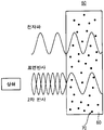
- FIG. 1 is a cross-sectional view schematically showing an electromagnetic wave absorber according to a comparative example.
- FIG. 2 is a cross-sectional view illustrating an electromagnetic wave absorber according to exemplary embodiments.
- FIG 3 is a cross-sectional view illustrating an electromagnetic wave absorber according to some exemplary embodiments.
- FIG. 4 is a diagram for describing a plating process of reinforcing fibers of an electromagnetic wave absorber according to exemplary embodiments.
- FIG. 5 is a Scanning Electron Microscope (SEM) image showing uncoated glass fibers and nickel coated glass fiber samples.
- FIG. 6 is Energy Dispersive Spectroscopy (EDS) graphs for the uncoated glass fibers and samples of FIG. 5.
- EDS Energy Dispersive Spectroscopy
- 8A and 8B are graphs showing the change in permittivity at the X-band frequency of nickel coated glass fiber prepreg.
- 9A and 9B are graphs showing the change in permeability of the nickel coated glass fiber prepreg at the X-band frequency.
- 11 is a graph showing the reflection loss in the nickel coated glass fiber prepreg multilayer composite material.
- FIG. 13 is a graph showing the interlaminar shear stress of nickel coated fiber prepreg samples with reference to ASTM D2344 specification.
- FIG. 1 is a cross-sectional view schematically showing an electromagnetic wave absorber according to a comparative example.
- the electromagnetic wave absorber 50 may include a matrix 60 and nanoparticles 70 dispersed in the substrate 60.
- Substrate 60 may include, for example, an epoxy based prepreg impregnated with fibers (eg, glass fibers).
- the nanoparticles 70 may include a carbon based material such as carbon black, carbon nano tube (CNT), carbon nanofiber, or the like. Electromagnetic waves incident on the electromagnetic wave absorber 50 may be absorbed or scattered by the nanoparticles 70.
- the viscosity in the substrate 60 increases, making dispersion of the nanoparticles 70 more difficult. Can lose.
- the volume of the fiber per unit volume of the electromagnetic wave absorber 50 may be reduced. Therefore, the mechanical properties of the electromagnetic wave absorber 50 can be reduced.
- FIG. 2 is a cross-sectional view illustrating an electromagnetic wave absorber according to exemplary embodiments.
- the electromagnetic wave absorber 100 may include a reinforcing fiber 210 impregnated in the substrate 200. Accordingly, the electromagnetic wave absorber 100 may be provided as a fiber impregnated prepreg based composite material.
- the substrate 200 may include a polymer resin such as an epoxy resin, a phenol resin, a polyimide resin, a poly acrylic resin, or the like.
- a thermosetting resin such as an epoxy resin may be used as the substrate 200.
- glass fibers or aromatic polyamide-based fibers may be used as the reinforcing fibers 210.
- aramid fibers such as kevlar fibers may be used as the reinforcing fibers 210.
- the metal magnetic coating layer 220 may be formed on the surface of the reinforcing fiber 210.
- the magnetic metal coating layer 220 may include ferromagnetic materials such as nickel (Ni), cobalt (Co), and iron (Fe). In some embodiments, the metal magnetic coating layer 220 may include nickel.
- the electromagnetic wave absorber 100 is based on the composite material impregnated with the reinforcing fiber 210, the electromagnetic wave absorber 100 may have improved mechanical properties (eg, shear stress, heat resistance, etc.). Therefore, it can be applied directly as a supporting structure of an aircraft or the like.
- a metal magnetic coating layer 220 including a ferromagnetic material is formed on the surface of the reinforcing fiber 210, and when electromagnetic waves are incident on the electromagnetic wave absorber 100 from the outside, the surroundings of the reinforcing fiber 210 are applied by Lenz's law. An eddy current can be formed at. Since the eddy current is formed in the reverse direction of the incident electromagnetic wave, the intensity of the electromagnetic wave transmitted through the electromagnetic wave absorber 100 may be weakened.
- the magnetic metal coating layer 220 may be formed through an electroless plating method, as described below with reference to FIG. 4.
- the depth at which current penetrates into the material may be referred to as a skin depth, and the thickness of the magnetic metal coating layer 220 may be smaller than the thickness of the skin. Therefore, the conductivity through the metal magnetic coating layer 220 is reduced, so that the reinforcing fiber 210 may be used as a material of the electromagnetic wave absorber 100.
- the thickness of the magnetic metal coating layer 220 may be controlled on the scale of several tens of nanometers, and the metal magnetic coating layer 220 may be formed to a thickness smaller than the thickness of the skin.
- the electromagnetic wave absorbing ability may be implemented through the metal magnetic coating layer 220 formed on the surface of the reinforcing fiber 210. Therefore, since the necessity of dispersing nanoparticles as in the comparative example is eliminated, the uncertainty of the electromagnetic wave absorbing ability such as non-uniform dispersion degree can be reduced.
- the magnetic metal coating layer 220 is provided in the substrate 200 together with the reinforcing fibers 210 in the form of a thin film, it is possible to secure a predetermined volume of the reinforcing fibers 210 with respect to the total volume of the electromagnetic wave absorber 100. have. Therefore, the electromagnetic wave absorbing ability can be realized without deteriorating the mechanical properties of the electromagnetic wave absorber 100.
- FIG 3 is a cross-sectional view illustrating an electromagnetic wave absorber according to some exemplary embodiments.
- the electromagnetic wave absorber 300 may have a multilayer structure including, for example, a first layer 310 and a second layer 320.
- the first layer 310 can include a first reinforcing fiber 510 impregnated in the first substrate 500.
- the first substrate 500 may include a thermosetting resin such as an epoxy resin, a phenol resin, or the like.
- the first reinforcing fiber 510 may include, for example, glass fiber or kevlar fiber.
- the first layer 310 may be provided as a prepreg composite material and serve as a support layer of the electromagnetic wave absorber 300.
- the second layer 320 may have a configuration and / or structure substantially the same as or similar to that of the electromagnetic wave absorber 100 illustrated in FIG. 2.
- the second layer 320 includes second reinforcing fibers 410 impregnated in the second substrate 400, and a metal magnetic coating layer 420 may be formed on the surface of the second reinforcing fibers 410.
- the second substrate 400 may include a thermosetting resin substantially the same as the first substrate 500. In some embodiments, the second substrate 400 may include a thermosetting resin different from the first substrate 500.
- the second reinforcing fiber 410 includes, for example, glass fiber or Kevlar fiber, and the metal magnetic coating layer 420 may be electroless plated coated to include a ferromagnetic material such as nickel, iron, and cobalt. It can be formed through.
- a ferromagnetic material such as nickel, iron, and cobalt. It can be formed through.
- the mechanical properties of the electromagnetic wave absorber 300 may be secured through the first layer 310 impregnated with the uncoated first reinforcing fiber 510.
- an electromagnetic wave absorbing ability may be realized through the metal magnetic coating layer 420 of the second layer 320.
- the electromagnetic wave absorber 300 is designed in a multilayer structure, for example, secondary reflection of electromagnetic waves through an interface between the first layer 310 and the second layer 320 is added, thereby further improving the electromagnetic wave absorbing ability. Can be.
- FIG. 4 is a diagram for describing a plating process of reinforcing fibers of an electromagnetic wave absorber according to exemplary embodiments.
- the magnetic metal coating layer 630 may be formed on the surface of the reinforcing fiber 620 through an electroless plating coating method.
- the magnetic metal coating layer 630 may be deposited on the surface of the reinforcing fiber 620 by immersing the reinforcing fiber 620 in the aqueous metal salt solution 610 accommodated in the plating bath 600.
- the metal salt aqueous solution 610 may include a metal salt compound and a reducing agent.
- a nickel salt compound may be used as the metal salt compound.
- the nickel salt compound may include nickel sulfate, nickel acetate or nickel chloride. These may be used alone or in combination of two or more.
- an auto catalytic plating process may be substantially performed.
- the metal magnetic coating layer 630 may be formed by the catalysis of the chemical energy and the deposited metal through the reducing agent without a separate electric energy supply.
- a uniform plating film may be formed on the surface of the reinforcing fiber 620. Therefore, it is possible to implement a uniform electromagnetic wave absorbing ability in the desired target frequency region over the entire region of the electromagnetic wave absorber.
- a compound optimized for nickel plating may be selected.
- a phosphate salt such as sodium hypophosphite or a boron compound such as methyl amine boron may be used as the reducing agent.
- concentration of the reducing agent is increased, the concentration of phosphorus (P) or boron (B) is increased, the plating rate may be increased.
- the magnetic metal coating layer 630 may include a nickel-phosphorus (Ni-P) alloy.
- the boron compound when used as the reducing agent, it may include a nickel-boron (Ni-B) alloy.
- the dopant such as P or B is included in the metal magnetic coating layer 630, mechanical properties such as hardness and wear resistance may be improved, for example, than the plating layer formed through electroplating.
- a self-catalytic plating process may be performed according to the following scheme.
- the metal salt aqueous solution 610 may further include a pH adjuster.
- the pH of the metal salt aqueous solution 610 may be maintained in the range of about 4 to about 6 by the pH adjusting agent.
- the pH regulator include sodium hydroxide or ammonia.
- the aqueous metal salt solution 610 may further include a stabilizer, a surfactant, and the like for protecting the plating bath 600 and preventing uneven deposition.
- stabilizer include heavy metal salt compounds such as lead (Pb) and cadmium (Cd).
- the reinforcing fibers 620 on which the magnetic metal layer 630 is formed may be taken out from the plating bath 600, and a heat treatment process may be further performed.
- a heat treatment process may be further performed.
- adhesion between the magnetic metal layer 630 and the reinforcing fiber 620 and the hardness of the magnetic metal layer 630 may be improved.
- the heat treatment may be performed at, for example, about 300 ° C. to about 500 ° C. for about 1 hour to about 2 hours.
- FIG. 5 is a Scanning Electron Microscope (SEM) image showing uncoated glass fibers and nickel coated glass fiber samples.
- FIG. 6 is Energy Dispersive Spectroscopy (EDS) graphs for the uncoated glass fibers and samples of FIG. 5.
- the nickel-plated metal magnetic coating layer may be formed on the glass fiber surface by the electroless plating method described with reference to FIG. 4.
- FIG. 7 is a graph for explaining the design of the dielectric constant to satisfy the antireflection condition at the target frequency.
- FIG. 7 shows the optimal permittivity design at a target frequency of 10 GHz via Cole-Cole Plot and the permittivity values of the samples in FIGS. 5 and 6.
- the optimal design values of the real part and the imaginary part of permittivity satisfying the antireflection condition at 10 GHz are indicated by sets of squares through a call-call plot. Can be.
- sample (c) having a nickel content of 0.23 at% intersects the optimum design curve.
- the optimum value of the permittivity may be set at a predetermined target frequency, for example, through a call-call plot, and the content and permittivity of the ferromagnetic material may be designed to be close to the optimum value.
- the content of the metal salt compound and the reducing agent may be adjusted such that the optimum value is close.
- FIGS. 8A and 8B are graphs showing the change in permittivity at the X-band frequency of nickel coated glass fiber prepreg. Specifically, FIGS. 8A and 8B show the real and imaginary parts of the dielectric constant of the uncoated glass fibers and samples in FIGS. 5 and 6, respectively.
- a ferromagnetic material such as nickel has a dielectric constant that is relatively variable according to a target frequency. Therefore, it is possible to implement the optimum dielectric constant design of the electromagnetic wave absorber according to the target frequency.
- FIGS. 9A and 9B are graphs showing the change in permeability at the nickel coated glass fiber prepreg X-band frequency. Specifically, FIGS. 9A and 9B show the real and imaginary parts of the permeability of the samples in FIGS. 5 and 6, respectively.
- the ferromagnetic samples have a large change in permeability according to frequency change.
- Electromagnetic wave absorbers can be designed by matching the input impedance while varying the thickness of each layer and the material used.
- the thickness of the electromagnetic wave absorber material may be about one quarter of the electromagnetic wave wavelength within the material.
- the dielectric constant or permeability of conventional insulators has a nearly constant value in the microwave band, so the condition of about one quarter of the electromagnetic wave wavelength is very limited.
- the permeability change is large in the microwave band, so that the range of the condition of about 1/4 of the electromagnetic wave wavelength in the material is broadened.
- a wideband electromagnetic wave absorber design can be implemented.
- FIG. 10 is a graph showing the reflection loss in the nickel coated glass fiber prepreg single layer composite material.
- FIG. 10 shows the reflection loss by the electromagnetic wave absorber as described with reference to FIG. 2.
- an electromagnetic wave absorber including nickel coated glass fibers and manufactured with a total thickness of 1.884 mm exhibited a return loss performance of about 15 dB at a target frequency of 10 GHz (effective reflection loss). : 10 dB).
- FIG. 11 is a graph showing the reflection loss in the nickel coated glass fiber prepreg multilayer composite material.
- FIG. 11 shows the reflection loss by the electromagnetic wave absorber of the multilayer structure as described with reference to FIG.
- the first layer of the electromagnetic wave absorber includes an epoxy / glass fiber prepreg, and a second layer including the nickel coated glass fiber prepreg is stacked on the first layer.
- the electromagnetic wave absorber was manufactured to a total thickness of 2.298 mm.
- the electromagnetic wave absorber showed a return loss performance of about 35 dB at a target frequency of 10 GHz.
- the reflection loss or the electromagnetic wave absorbing ability can be further improved by designing the electromagnetic wave absorber in a multilayer structure.
- the adjustable dielectric constant and permeability can be set for each layer for optimal absorption design, so that the electromagnetic wave absorption ability can be more optimized.
- FIG. 12 is a graph showing return loss in nickel coated Kevlar fiber prepreg multilayer composites.
- FIG. 12 shows the reflection loss by the electromagnetic wave absorber of the multilayer structure as described with reference to FIG.
- a first layer of the electromagnetic wave absorber includes an epoxy / glass fiber prepreg, and a second layer including a nickel coated kevlar fiber prepreg is stacked on the first layer.
- the electromagnetic wave absorber was manufactured to a total thickness of 3.218 mm.
- the electromagnetic wave absorber showed a return loss performance of about 45 dB at a target frequency of 10 GHz.
- FIG. 13 is a graph showing the interlaminar shear stress of nickel coated fiber prepreg samples with reference to ASTM D2344 specification.
- FIG. Specifically, FIG. 13 is a graph showing interlaminar shear strength measurements of prepregs comprising uncoated and nickel coated glass fiber samples in FIGS. 5 and 6.
- the prepreg including nickel-coated glass fibers compared to the prepreg (left column) impregnated with the non-nickel glass fibers showed substantially the same or similar interlaminar shear stress. Accordingly, it can be confirmed that by forming the metal magnetic coating layer, it is possible to remove the uncertainty of the electromagnetic wave absorbing ability and to secure a predetermined structural stability.
- the electromagnetic wave absorber according to the exemplary embodiments described above may be applied to advanced mechanical fields such as aerospace where stealth technology is applied.
- first layer 320 second layer
- first base material 510 first reinforcing fiber
- plating bath 610 metal salt aqueous solution
Landscapes
- Engineering & Computer Science (AREA)
- Physics & Mathematics (AREA)
- Electromagnetism (AREA)
- Microelectronics & Electronic Packaging (AREA)
- Textile Engineering (AREA)
- Shielding Devices Or Components To Electric Or Magnetic Fields (AREA)
- Laminated Bodies (AREA)
Abstract
전자파 흡수체는 제1 기재 내에 함침된 제1 강화 섬유를 포함하는 제1 층, 및 제1 층 상에 적층되며 제2 기재 및 제2 기재 내에 함침되며 금속 자성 코팅층으로 도금된 제2 강화 섬유를 포함하는 제2 층을 포함한다. 기계적 물성을 저하시키지 않으면서 금속 자성 코팅층에 의해 전자파 흡수능을 낮은 불확실도로 구현할 수 있다.
Description
본 발명은 금속 코팅된 섬유를 포함하는 전자파 흡수체 및 이의 제조 방법에 관한 것이다. 보다 상세하게는, 본 발명은 금속 자성 코팅층이 형성된 섬유를 포함하는 전자파 흡수체 및 이의 제조 방법에 관한 것이다.
전자파 흡수 특성을 갖는 복합재료는 예를 들면, 스텔스 기술에 적용되고 있다. 상기 스텔스 기술에 있어서, 전자파(Electromagnetic Wave)를 흡수 또는 산란시켜 레이더에 포착되지 않도록 하는 기술이 채용되고 있다.
상기 스텔스 기술을 항공기에 구현하기 위한 방법으로서 형상(shaping) 방법, RAM(Radar Absorbing Material) 방법, 및 RAS(Radar Absorbing Structure) 방법 등을 들 수 있다.
상기 형상 방법은 레이더로부터 입사되는 전자파를 레이더 방향과 다른 방향으로 반사시키도록 항공기 외형을 성형하는 방법이다. 그러나, 항공기의 공기역학적 특성을 손상시키는 문제가 있으며, 또한 형상 설계만으로는 충분한 스텔스 성능이 확보되지 않을 수 있다.
상기 RAM 방법은 전자파 흡수 물질을 항공기 표면에 직접 도포하는 방법이다. 그러나, 예를 들면 상기 RAM 방법에 의해 도포된 전자파 흡수막은 내구성이 떨어져 짧은 주기로 유지 보수가 필요하다는 문제가 있다.
상기 RAS 방법에 있어서, 상기 RAS 방법의 내구성 문제를 보완하기 위해 전자파 흡수체를 예를 들면, 항공기의 구조물로 직접 채용할 수 있다. 이에 따라, 상기 전자파 흡수체는 스텔스 기능을 수행함과 동시에 항공기의 지지 구조물로 제공될 수 있다.
예를 들면, 특허문헌 1(대한민국 등록특허공보 제10-1349029호)은 매트릭스 내에 나노입자를 분산시킨 복합재료를 개시하고 있다.
본 발명의 일 과제는 우수한 성능의 전자파 흡수체를 제공하는 것이다.
본 발명의 일 과제는 우수한 성능의 전자파 흡수체의 제조 방법을 제공하는 것이다.
다만, 본 발명이 해결하고자 하는 과제는 상기 언급된 과제에 한정되는 것이 아니며, 본 발명의 사상 및 영역으로부터 벗어나지 않는 범위에서 다양하게 확장될 수 있을 것이다.
상술한 본 발명의 일 과제를 달성하기 위한 본 발명의 예시적인 실시예들에 따른 전자파 흡수체는 제1 기재 내에 함침된 제1 강화 섬유를 포함하는 제1 층, 및 상기 제1 층 상에 적층되며 제2 기재 및 상기 제2 기재 내에 함침되며 금속 자성 코팅층으로 도금된 제2 강화 섬유를 포함하는 제2 층을 포함할 수 있다.
예시적인 실시예들에 있어서, 상기 금속 자성 코팅층은 니켈(Ni), 코발트(Co) 또는 철(Fe) 중에서 선택되는 강자성체를 포함할 수 있다. 이들을 단독으로 혹은 2 이상이 조합되어 사용될 수 있다.
예시적인 실시예들에 있어서, 상기 제1 기재 및 상기 제2 기재는 열경화성 수지를 포함할 수 있다.
예시적인 실시예들에 있어서, 상기 제1 강화 섬유 및 상기 제2 강화 섬유는 유리 섬유 또는 케블라(kevlar) 섬유를 포함할 수 있다.
예시적인 실시예들에 있어서, 상기 제1 강화 섬유는 미코팅된 섬유를 포함할 수 있다.
상술한 본 발명의 일 과제를 달성하기 위한 본 발명의 예시적인 실시예들에 따른 전자파 흡수체의 제조 방법에 따르면, 목표 주파수에 따른 유전율 또는 투자율을 설정할 수 있다. 강화 섬유 표면 상에 상기 유전율 또는 상기 투자율을 갖는 함량 또는 두께로 금속 자성 코팅층을 형성할 수 있다. 상기 금속 자성 코팅층이 형성된 상기 강화 섬유를 열경화성 수지 내에 함침시킬 수 있다.
예시적인 실시예들에 있어서, 상기 목표 주파수에 따른 상기 유전율 또는 상기 투자율을 설정을 위해 상기 목표 주파수에 따른 최적 유전율의 실수부 및 허수부의 조합을 생성할 수 있다.
예시적인 실시예들에 있어서, 상기 최적 유전율의 상기 실수부 및 상기 허수부의 조합 생성은 상기 전자파 흡수체에서의 무반사 조건을 만족하는 콜-콜 플롯(Cole-Cole plot)을 활용할 수 있다.
예시적인 실시예들에 있어서, 상기 금속 자성 코팅체는 상기 강화 섬유를 금속염 화합물 및 환원제를 포함하는 금속염 수용액 내에 함침시켜 무전해 도금 코팅을 통해 형성될 수 있다.
예시적인 실시예들에 있어서, 상기 금속염 화합물은 니켈 염 화합물을 포함하며, 상기 환원제는 인산 염 또는 붕소 화합물을 포함할 수 있다.
예시적인 실시예들에 있어서, 상기 금속 자성 코팅층은 니켈-인(Ni-P) 합금 또는 니켈-붕소(Ni-B) 합금을 포함할 수 있다.
상술한 바와 같이 본 발명의 예시적인 실시예들에 따르면, 전자파 흡수체의 기재 내에 금속 자성 코팅층이 형성된 강화 섬유를 제공할 수 있다. 전자파 흡수를 위한 재료를 상기 강화 섬유에 코팅층으로 제공함으로써, 불균일 분산과 같은 불확실성을 제거할 수 있다. 또한, 타겟 주파수에 따른 최적 유전율 또는 투자율에 따라 상기 금속 자성 코팅층의 함량 및/또는 두께를 조절할 수 있다.
도 1은 비교예에 따른 전자파 흡수체를 개략적으로 도시한 단면도이다.
도 2는 예시적인 실시예들에 따른 전자파 흡수체를 나타내는 단면도이다.
도 3은 일부 예시적인 실시예들에 따른 전자파 흡수체를 나타내는 단면도이다.
도 4는 예시적인 실시예들에 따른 전자파 흡수체의 강화 섬유의 도금 공정을 설명하기 위한 도면이다.
도 5는 미코팅 유리 섬유 및 니켈 코팅된 유리 섬유 샘플들을 나타내는 주사 전자 현미경(Scanning Electron Microscope: SEM) 이미지들이다.
도 6은 도 5의 미코팅 유리 섬유 및 샘플들에 대한 에너지 분광(Energy Dispersive Spectroscopy: EDS) 그래프들이다.
도 7은 목표 주파수에서 무반사 조건을 만족하기 위한 유전율의 설계를 설명하기 위한 그래프이다.
도 8a 및 도 8b는 니켈 코팅된 유리섬유 프리프레그의 X-밴드 주파수에서의 유전율 변화를 나타내는 그래프들이다.
도 9a 및 도 9b는 니켈 코팅된 유리섬유 프리프레그의 X-밴드 주파수에서의 투자율 변화를 나타내는 그래프들이다.
도 10은 니켈 코팅된 유리섬유 프리프레그 단층 복합재료에서의 반사손실을 나타내는 그래프이다.
도 11은 니켈 코팅된 유리섬유 프리프레그 복층 복합재료에서의 반사손실을 나타내는 그래프이다.
도 12는 니켈 코팅된 케블라 섬유 프리프레그 복층 복합재료에서의 반사손실을 나타내는 그래프이다.
도 13은 ASTM D2344 규격을 참고하여 니켈 코팅된 섬유 프리프레그 샘플들의 층간 전단 응력을 나타낸 그래프이다.
이하, 첨부한 도면을 참조하여 본 발명의 실시예에 대해 상세히 설명한다. 본 발명은 다양한 변경을 가할 수 있고 여러 가지 형태를 가질 수 있는 바, 특정 실시예들을 예시하고 본문에 상세하게 설명하고자 한다. 그러나 이는 본 발명을 특정한 개시 형태에 대해 한정하려는 것이 아니며, 본 발명의 사상 및 기술 범위에 포함되는 모든 변경, 균등물 내지 대체물을 포함하는 것으로 이해되어야 한다. 첨부된 도면에 있어서, 구조물들의 치수는 본 발명의 명확성을 기하기 위하여 실제보다 확대하여 도시한 것이다.
본 출원에서 사용한 용어는 단지 특정한 실시예를 설명하기 위해 사용된 것으로, 본 발명을 한정하려는 의도가 아니다. 단수의 표현은 문맥상 명백하게 다르게 뜻하지 않는 한, 복수의 표현을 포함한다. 본 출원에서, "포함하다" 또는 "가지다" 등의 용어는 명세서상에 기재된 특징, 숫자, 단계, 동작, 구성요소 또는 이들을 조합한 것이 존재함을 지정하려는 것이지, 하나 또는 그 이상의 다른 특징들이나 숫자, 단계, 동작, 구성요소 또는 이들을 조합한 것들의 존재 또는 부가 가능성을 미리 배제하지 않는 것으로 이해되어야 한다.
다르게 정의되지 않는 한, 기술적이거나 과학적인 용어를 포함해서 여기서 사용되는 모든 용어들은 본 발명이 속하는 기술분야에서 통상의 지식을 가진 자에 의해 일반적으로 이해되는 것과 동일한 의미를 가지고 있다. 일반적으로 사용되는 사전에 정의되어 있는 것과 같은 용어들은 관련 기술의 문맥 상 가지는 의미와 일치하는 의미를 가지는 것으로 해석되어야 하며, 본 출원에서 명백하게 정의하지 않는 한, 이상적이거나 과도하게 형식적인 의미로 해석되지 않는다.
도 1은 비교예에 따른 전자파 흡수체를 개략적으로 도시한 단면도이다.
도 1을 참조하면, 비교예에 따른 전자파 흡수체(50)는 기재(matrix)(60), 및 기재(60) 내에 분산된 나노 입자들(70)을 포함할 수 있다.
기재(60)는 예를 들면, 섬유(예를 들면, 유리 섬유)가 함침된 에폭시(epoxy) 기반의 프리프레그를 포함할 수 있다. 나노 입자들(70)은 카본 블랙(carbon black), 탄소 나노 튜브(carbon nano tube: CNT), 탄소 나노 섬유 등과 같은 탄소 계열 물질을 포함할 수 있다. 나노 입자들(70)에 의해 전자파 흡수체(50)에 입사된 전자파가 흡수 또는 산란될 수 있다.
예를 들면, 도 1에 도시된 바와 같이, 전자파가 전자파 흡수체(50)의 전면으로 입사되는 경우, 상기 전자파중 일부는 상기 전면으로부터 표면 반사되며, 일부는 전자파 흡수체(50)의 이면으로부터 2차 반사될 수 있다. 상기 표면 반사 및 2차 반사된 전자파들이 서로 상쇄 간섭을 일으켜 상기 전자파를 제거할 수 있다.
그러나, 비교예의 전자파 흡수체(50)의 경우, 기재(60) 내에 다량의 나노 입자들(70)을 분산시켜야 하므로 작업 조건에 따라 분산도가 변하는 불확실성이 증가하게 된다. 따라서, 원하는 주파수 대역대의 전자파 흡수를 위한 정밀한 흡수체 설계가 곤란하다.
또한, 전자파 흡수체(50)의 강도를 증가시키기 위해 기재(60) 내에 필러(filler)와 같은 재료가 혼합되는 경우, 기재(60) 내의 점도가 증가하여 나노 입자들(70)의 분산이 더욱 어려워질 수 있다. 추가적으로, 전자파 흡수 성능을 향상시키기 위해 나노 입자들(70)의 함량을 증가시키는 경우, 전자파 흡수체(50)의 단위 부피당 상기 섬유의 체적이 감소될 수 있다. 따라서, 전자파 흡수체(50)의 기계적 물성을 저하시킬 수 있다.
도 2는 예시적인 실시예들에 따른 전자파 흡수체를 나타내는 단면도이다.
도 2를 참조하면, 전자파 흡수체(100)는 기재(200) 내에 함침된 강화 섬유(210)를 포함할 수 있다. 이에 따라, 전자파 흡수체(100)는 섬유 함침 프리프레그기반 복합재료로서 제공될 수 있다.
기재(200)는 에폭시 수지, 페놀 수지, 폴리이미드 수지, 폴리 아크릴 수지 등과 같은 고분자 레진을 포함할 수 있다. 일부 실시예들에 있어서, 기재(200)로서 에폭시 수지와 같은 열경화성 수지를 사용할 수 있다.
예시적인 실시예들에 따르면, 강화 섬유(210)로서 유리 섬유 또는 방향족 폴리아미드 계열의 섬유를 사용할 수 있다. 일부 실시예들에 있어서, 강화 섬유(210)로서 케블라(kevlar) 섬유와 같은 아라미드 섬유를 사용할 수 있다.
강화 섬유(210)의 표면 상에는 금속 자성 코팅층(220)이 형성될 수 있다.
예시적인 실시예들에 따르면, 금속 자성 코팅층(220)은 니켈(Ni), 코발트(Co), 철(Fe)과 같은 강자성체(ferromagnetic)를 포함할 수 있다. 일부 실시예들에 있어서, 금속 자성 코팅층(220)은 니켈을 포함할 수 있다.
상술한 바와 같이, 전자파 흡수체(100)는 강화 섬유(210)가 함침된 복합 재료를 기반으로 하므로, 향상된 기계적 물성(예를 들면, 전단 응력, 내열성 등)을 가질 수 있다. 따라서, 항공기 등의 지지 구조물로서 직접 적용될 수 있다.
또한, 강자성체를 포함하는 금속 자성 코팅층(220)이 강화 섬유(210) 표면에 형성되어, 외부에서 전자파가 전자파 흡수체(100)로 입사되는 경우 렌츠(Lentz)의 법칙에 의해 강화 섬유(210) 주변에서 와전류(eddy current)가 형성될 수 있다. 입사된 상기 전자파의 역방향으로 상기 와전류가 형성되므로, 전자파 흡수체(100)로 투과되는 전자파의 세기가 약화될 수 있다.
예시적인 실시예들에 따르면, 금속 자성 코팅층(220)은 도 4를 참조로 후술하는 바와 같이, 무전해 도금 코팅법을 통해 형성될 수 있다.
예를 들면, 재료 내부로 전류가 침투하는 깊이를 표피 두께(skin depth)로 지칭할 수 있으며, 금속 자성 코팅층(220)의 두께는 상기 표피 두께 보다 작을 수 있다. 따라서, 금속 자성 코팅층(220)을 통한 전도도가 감소하여 강화섬유(210)를 전자파 흡수체(100)의 재료로서 활용할 수 있다.
상기 무전해 도금 코팅법을 통해 수십 나노미터 스케일로 금속 자성 코팅층(220)의 두께를 조절할 수 있으며, 상기 표피 두께보다 작은 두께로 금속 자성 코팅층(220)을 형성할 수 있다.
상술한 예시적인 실시예들에 따르면, 전자파 흡수능을 강화 섬유(210) 표면 상에 형성된 금속 자성 코팅층(220)을 통해 구현할 수 있다. 따라서, 비교예에서와 같은 나노 입자 분산의 필요성이 제거되므로, 불균일 분산도와 같은 전자파 흡수능의 불확실성이 감소할 수 있다.
또한, 금속 자성 코팅층(220)은 박막 형태로 강화 섬유(210)와 함께 기재(200) 내부에 제공되므로, 전자파 흡수체(100)의 총 부피 대비 강화 섬유(210)의 소정의 체적을 확보할 수 있다. 따라서, 전자파 흡수체(100)의 기계적 물성을 저하시키지 않으면서 상기 전자파 흡수능을 구현할 수 있다.
도 3은 일부 예시적인 실시예들에 따른 전자파 흡수체를 나타내는 단면도이다.
도 3을 참조하면, 전자파 흡수체(300)는 예를 들면, 제1 층(310) 및 제2 층(320)을 포함하는 복층 구조를 가질 수 있다.
제1 층(310)은 제1 기재(500) 내에 함침된 제1 강화 섬유(510)를 포함할 수 있다. 제1 기재(500)는 에폭시 수지, 페놀 수지 등과 같은 열경화성 수지를 포함할 수 있다. 제1 강화 섬유(510)는 예를 들면, 유리 섬유 또는 케블라 섬유를 포함할 수 있다.
제1 층(310)은 상술한 바와 같이, 프리프레그 복합 재료로서 제공되어 전자파 흡수체(300)의 지지층으로 기능할 수 있다.
제2 층(320)은 도 2에 도시된 전자파 흡수체(100)와 실질적으로 동일하거나 유사한 구성 및/또는 구조를 가질 수 있다.
제2 층(320)은 제2 기재(400) 내에 함침된 제2 강화 섬유(410)를 포함하며, 제2 강화 섬유(410) 표면 상에는 금속 자성 코팅층(420)이 형성될 수 있다.
제2 기재(400)는 제1 기재(500)와 실질적으로 동일한 열경화성 수지를 포함할 수 있다. 일부 실시예들에 있어서, 제2 기재(400)는 제1 기재(500)와 다른 열경화성 수지를 포함할 수도 있다.
상술한 바와 같이, 제2 강화 섬유(410)는 예를 들면, 유리 섬유 또는 케블라 섬유를 포함하며, 금속 자성 코팅층(420)은 니켈, 철, 코발트와 같은 강자성체를 포함하도록 무전해 도금 코팅법을 통해 형성될 수 있다.
상술한 예시적인 실시예들에 따르면, 미코팅된 제1 강화 섬유(510)가 함침된 제1 층(310)을 통해 전자파 흡수체(300)의 기계적 물성을 확보할 수 있다. 또한, 제2 층(320)에서의 금속 자성 코팅층(420)을 통해 전자파 흡수능을 구현할 수 있다.
또한, 전자파 흡수체(300)가 복층 구조로 설계됨에 따라, 예를 들면, 제1 층(310) 및 제2 층(320)의 계면을 통한 전자파의 2차 반사가 추가되어 상기 전자파 흡수능이 보다 향상될 수 있다.
도 4는 예시적인 실시예들에 따른 전자파 흡수체의 강화 섬유의 도금 공정을 설명하기 위한 도면이다.
도 4를 참조하면, 강화 섬유(620) 표면에 무전해 도금 코팅법을 통해 금속 자성 코팅층(630)을 형성할 수 있다.
도 4에 도시된 바와 같이, 도금조(600) 내에 수용된 금속염 수용액(610)에 강화 섬유(620)를 침지시켜 강화 섬유(620) 표면에 금속 자성 코팅층(630)을 석출시킬 수 있다.
금속염 수용액(610)은 금속염 화합물 및 환원제를 포함할 수 있다. 일부 실시예들에 있어서, 상기 금속염 화합물로서 니켈 염 화합물을 사용할 수 있다. 예를 들면, 상기 니켈 염 화합물은 황산 니켈, 초산 니켈 또는 염화 니켈을 포함할 수 있다. 이들은 단독으로 혹은 2 이상이 조합되어 사용될 수 있다.
금속염 수용액(610) 내에 상기 환원제를 포함시킴으로써, 실질적으로 자기 촉매 도금(auto catalytic plating) 공정이 진행될 수 있다. 상기 자기 촉매 도금 공정에 의해, 별도의 전기 에너지 공급 없이 상기 환원제를 통한 화학 에너지 및 석출되는 금속의 촉매 작용에 의해 금속 자성 코팅층(630)이 형성될 수 있다.
따라서, 불균일한 전류 분포의 문제가 제거되므로 균일한 도금막이 강화 섬유(620) 표면에 형성될 수 있다. 따라서, 전자파 흡수체 전체 영역에 걸쳐 원하는 타겟 주파수 영역에서 균일한 전자파 흡수능을 구현할 수 있다.
상기 환원제로서 니켈 도금에 최적화된 화합물을 선택할 수 있다. 일부 실시예들에 있어서, 상기 환원제로서 차아인산나트륨과 같은 인산 염 또는 메틸 아민보론과 같은 붕소 화합물이 사용될 수 있다. 상기 환원제의 농도가 증가하면, 인(P) 또는 붕소(B)의 농도가 증가하며, 도금 속도가 증가될 수 있다.
예를 들어, 상기 환원제로서 차아인산나트륨이 사용되는 경우 금속 자성 코팅층(630)은 니켈-인(Ni-P) 합금을 포함할 수 있다. 상기 환원제로서 상기 붕소 화합물이 사용되는 경우 니켈-붕소(Ni-B) 합금을 포함할 수 있다. P 또는 B와 같은 도펀트가 금속 자성 코팅층(630)에 포함됨에 따라, 예를 들면 전기도금을 통해 형성되는 도금층보다 경도 및 내마모성과 같은 기계적 물성이 향상될 수 있다.
예를 들면, 상기 금속염 화합물 및 상기 환원제로서 각각 황산 니켈 및 차아인산나트륨을 사용하는 경우, 아래의 반응식에 의한 자기 촉매 도금 공정이 진행될 수 있다.
[반응식]
NiSO4 + 2NaH2PO2 +2HO → Ni + 2NaH2PO3 + H2 + H2SO4
일부 예시적인 실시예들에 있어서, 금속염 수용액(610)에는 pH 조절제가 더 포함될 수 있다. 상기 pH 조절제에 의해 금속염 수용액(610)의 pH가 예를 들면, 약 4 내지 약 6 범위로 유지될 수 있다. 상기 pH 조절제의 예로서 수산화나트륨 또는 암모니아를 들 수 있다.
일부 실시예들에 있어서, 금속염 수용액(610)은 도금조(600) 보호 및 불균일 석출 방지를 위한 안정제, 계면 활성제 등을 더 포함할 수도 있다. 상기 안정제의 예로서 납(Pb), 카드뮴(Cd)과 같은 중금속 염 화합물을 들 수 있다.
일부 예시적인 실시예들에 따라서, 상술한 무전해 도금 코팅 수행 후 금속 자성층(630)이 형성된 강화 섬유(620)를 도금조(600)로부터 취출하고, 열처리 공정을 추가로 수행할 수 있다. 상기 열처리에 의해 금속 자성층(630) 및 강화 섬유(620) 사이의 밀착성, 및 금속 자성층(630)의 경도가 향상될 수 있다. 상기 열처리는 예를 들면, 약 300℃ 내지 약 500℃ 온도에서 약 1 시간 내지 약 2 시간 동안 수행될 수 있다.
도 5는 미코팅 유리 섬유 및 니켈 코팅된 유리 섬유 샘플들을 나타내는 주사 전자 현미경(Scanning Electron Microscope: SEM) 이미지들이다. 도 6은 도 5의 미코팅 유리 섬유 및 샘플들에 대한 에너지 분광(Energy Dispersive Spectroscopy: EDS) 그래프들이다.
도 5 및 도 6을 참조하면, 예를 들면 도 4를 참조로 설명한 무전해 도금 코팅법에 의해 유리 섬유 표면에 니켈 도금된 금속 자성 코팅층이 형성되었음을 확인할 수 있다.
도 5 및 도 6에 도시된 바와 같이, 미코팅 유리 섬유(uncoated glass fabric)에서는 실질적으로 니켈의 함량이 측정되지 않았다. 그러나, 샘플 (a) 내지 (c)에서는 약 0.09 원자퍼센트(at%) 내지 약 0.42 at%, 또는 약 0.28 중량퍼센트(wt%) 내지 약 1.4 wt%의 함량으로 수십 나노 스케일의 니켈 코팅층이 형성되었음을 확인할 수 있다.
도 7은 목표 주파수에서 무반사 조건을 만족하기 위한 유전율의 설계를 설명하기 위한 그래프이다. 예를 들면, 도 7은 콜-콜 플롯(Cole-Cole Plot)을 통해 목표 주파수 10 GHz에서의 최적 유전율 설계 및 도 5 및 도 6에서의 샘플들의 유전율 값을 표시하고 있다.
도 7을 참조하면, 콜-콜 플롯을 통해 10 GHz에서의 무반사 조건을 만족하는 유전율(permittivity)의 실수부(real part) 및 허수부(imaginary part)의 최적 설계 값이 사각형들의 집합들로 표시될 수 있다.
도 7에 도시된 바와 같이, 0.23 at%의 니켈 함량을 갖는 (c) 샘플이 상기 최적 설계 곡선과 교차함을 알 수 있다.
상술한 바와 같이, 소정의 타겟 주파수에서 예를 들면, 콜-콜 플롯을 통해 유전율의 최적값을 설정하고, 상기 최적값에 근접하도록 강자성체의 함량 및 유전율을 설계할 수 있다.
예시적인 실시예들에 따르면, 도 4를 참조로 설명한 금속염 수용액에 있어서, 상기 최적값이 근접하도록 상기 금속염 화합물 및 상기 환원제의 함량을 조절할 수 있다.
도 8a 및 도 8b는 니켈 코팅된 유리섬유 프리프레그의 X-밴드 주파수에서의 유전율 변화를 나타내는 그래프들이다. 구체적으로, 도 8a 및 도 8b는 각각 도 5 및 도 6에서의 미코팅 유리 섬유 및 샘플들의 유전율의 실수부 및 허수부를 도시하고 있다.
도 8a 및 도 8b에 도시된 바와 같이 니켈과 같은 강자성체의 경우 목표 주파수에 따라 상대적으로 가변적인 유전율을 갖는다. 따라서, 타겟 주파수에 따라 전자파 흡수체의 최적 유전율 설계를 구현할 수 있다.
도 9a 및 도 9b는 니켈 코팅된 유리섬유 프리프레그 X-밴드 주파수에서의 투자율 변화를 나타내는 그래프들이다. 구체적으로, 도 9a 및 도 9b는 각각 도 5 및 도 6에서의 샘플들의 투자율(permeability)의 실수부 및 허수부를 도시하고 있다.
도 9a 및 도 9b에 도시된 바와 같이, 강자성체 샘플들은 주파수 변화에 따라 투자율의 변화가 큼을 알 수 있다.
전자파 흡수체는 사용하는 재료와 각 층의 두께를 변화시켜가며 입력 임피던스를 정합시켜 설계될 수 있다. 상기 전자파 흡수체에 있어서, 설계한 입력 임피던스가 자유 공간의 고유 임피던스에 가까울수록 반사 손실(예를 들면, 전자파 흡수능)이 우수하다고 할 수 있다. 예를 들면, 목표 주파수 대역에서 전자파 흡수체의 성능을 최적화하려면 전자파 흡수체 재료의 두께는 상기 재료 내에서 전자파 파장의 약 1/4이 될 수 있다. 그러나, 통상적인 절연체의 유전율 또는 투자율은 마이크로파 대역에서 거의 일정한 값을 가지고 있으므로 전자파 파장의 약 1/4이 되는 조건이 매우 제한적이다.
하지만, 상술한 강자성체가 전자파 흡수체의 재료로 채용되는 경우 도 9a 및 도 9b에 도시된 바와 같이 마이크로파 대역에서 투자율의 변화가 크므로 재료 내에서 전자파 파장의 약 1/4이 되는 조건의 범위를 넓힐 수 있으며, 광대역 전자파 흡수체 설계가 구현될 수 있다.
도 10은 니켈 코팅된 유리섬유 프리프레그 단층 복합재료에서의 반사손실을 나타내는 그래프이다. 예를 들면, 도 10은 도 2를 참조로 설명한 바와 같은 전자파 흡수체에 의한 반사 손실을 도시하고 있다.
도 10을 참조하면, 니켈 코팅된 유리 섬유를 포함하며, 1.884 mm의 총 두께로 제작된 전자파 흡수체에 있어서, 타겟 주파수 10 GHz에서 약 15 dB의 반사 손실(return loss) 성능을 보였다(유효 반사 손실: 10 dB).
도 11은 니켈 코팅된 유리섬유 프리프레그 복층 복합재료에서의 반사손실을 나타내는 그래프이다. 예를 들면, 도 11은 도 3을 참조로 설명한 바와 같은 복층 구조의 전자파 흡수체에 의한 반사 손실을 도시하고 있다.
도 11을 참조하면, 상기 전자파 흡수체의 제1 층은 에폭시/유리 섬유 프리프레그를 포함하며, 상기 제1 층 상에 니켈 코팅된 유리 섬유 프리프레그를 포함하는 제2 층이 적층되었다. 상기 전자파 흡수체는 총 2.298 mm의 두께로 제작되었다. 상기 전자파 흡수체는 타겟 주파수 10 GHz에서 약 35 dB의 반사 손실(return loss) 성능을 보였다.
도 11에 도시된 바와 같이, 전자파 흡수체를 복층 구조로 설계함으로써 반사 손실, 또는 전자파 흡수능을 더욱 향상시킬 수 있다. 예를 들면, 최적의 흡수능 설계를 위해 조절 가능한 유전율, 투자율과 같은 변수가 각 층별로 설정 가능하므로 상기 전자파 흡수능이 보다 최적화될 수 있다.
도 12는 니켈 코팅된 케블라 섬유 프리프레그 복층 복합재료에서의 반사손실을 나타내는 그래프이다. 예를 들면, 도 12는 도 3을 참조로 설명한 바와 같은 복층 구조의 전자파 흡수체에 의한 반사 손실을 도시하고 있다.
도 12를 참조하면, 상기 전자파 흡수체의 제1 층은 에폭시/유리 섬유 프리프레그를 포함하며, 상기 제1 층 상에 니켈 코팅된 케블라 섬유 프리프레그를 포함하는 제2 층이 적층되었다. 상기 전자파 흡수체는 총 3.218 mm의 두께로 제작되었다. 상기 전자파 흡수체는 타겟 주파수 10 GHz에서 약 45 dB의 반사 손실(return loss) 성능을 보였다.
도 13은 ASTM D2344 규격을 참고하여 니켈 코팅된 섬유 프리프레그 샘플들의 층간 전단 응력을 나타낸 그래프이다. 구체적으로 도 13은 도 5 및 6에서의 미코팅 유리 섬유 및 니켈 코팅된 유리 섬유 샘플들을 포함하는 프리프레그의 층간 전단 응력(interlaminar shear strength) 측정치를 나타내는 그래프이다.
도 13을 참조하면, 니켈이 코팅되지 않은 유리섬유가 함침된 프리프레그(좌측 칼럼) 대비 니켈이 코팅된 유리섬유를 포함하는 프리프레그의 경우 실질적으로 동일하거나 유사한 층간 전단 응력이 나타남을 알 수 있다. 따라서, 금속 자성 코팅층을 형성함으로써 전자파 흡수능의 불확실성을 제거함과 동시에, 소정의 구조적 안정성을 확보할 수 있음을 확인할 수 있다.
예시적인 실시예들에 따르면, ASTM 규격에 따른 강화섬유 함침 프리프레그의 층간 전단 응력 대비 금속 자성 코팅층 형성 후의 층간 전단 응력을 소정의 범위 내로 조절하여 전자파 흡수체의 기계적 물성의 적합성을 확보할 수 있다.
전술한 예시적인 실시예들에 따른 전자파 흡수체는 스텔스 기술이 적용되는 항공 우주 분야와 같은 첨단 기계 분야에 적용될 수 있다.
이상에서는 본 발명의 실시예들을 참조하여 설명하였지만, 해당 기술 분야의 숙련된 당업자는 하기의 특허 청구의 범위에 기재된 본 발명의 사상 및 영역으로부터 벗어나지 않는 범위 내에서 본 발명을 다양하게 수정 및 변경시킬 수 있음을 이해할 수 있을 것이다.
*부호의 설명*
50, 100, 300: 전자파 흡수체 60, 200: 기재
70: 나노 입자 210, 620: 강화 섬유
220, 420, 630: 금속 자성 코팅층
310: 제1 층 320: 제2 층
400: 제2 기재 410: 제2 강화 섬유
500: 제1 기재 510: 제1 강화 섬유
600: 도금조 610: 금속염 수용액
Claims (11)
- 제1 기재 내에 함침된 제1 강화 섬유를 포함하는 제1 층; 및상기 제1 층 상에 적층되며,제2 기재; 및상기 제2 기재 내에 함침되며 금속 자성 코팅층으로 도금된 제2 강화 섬유를 포함하는 제2 층을 포함하는 전자파 흡수체.
- 제1항에 있어서, 상기 금속 자성 코팅층은 니켈(Ni), 코발트(Co) 또는 철(Fe) 중에서 선택되는 적어도 하나의 강자성체를 포함하는 전자파 흡수체.
- 제1항에 있어서, 상기 제1 기재 및 상기 제2 기재는 열경화성 수지를 포함하는 전자파 흡수체.
- 제1항에 있어서, 상기 제1 강화 섬유 및 상기 제2 강화 섬유는 유리 섬유 또는 케블라(kevlar) 섬유를 포함하는 전자파 흡수체.
- 제4항에 있어서, 상기 제1 강화 섬유는 미코팅된 상기 유리 섬유 또는 상기 케블라 섬유를 포함하는 전자파 흡수체.
- 목표 주파수에 따른 유전율 또는 투자율을 설정하는 단계;강화 섬유 표면 상에 상기 유전율 또는 상기 투자율을 갖는 함량 또는 두께로 금속 자성 코팅층을 형성하는 단계; 및상기 금속 자성 코팅층이 형성된 상기 강화 섬유를 열경화성 수지 내에 함침시키는 단계를 포함하는 전자파 흡수체의 제조 방법.
- 제6항에 있어서, 상기 목표 주파수에 따른 상기 유전율 또는 상기 투자율을 설정하는 단계는 상기 목표 주파수에 따른 최적 유전율의 실수부 및 허수부의 조합을 생성하는 단계를 포함하는 전자파 흡수체의 제조 방법.
- 제7항에 있어서, 상기 최적 유전율의 상기 실수부 및 상기 허수부의 조합을 생성하는 단계는 상기 전자파 흡수체에서의 무반사 조건을 만족하는 콜-콜 플롯(Cole-Cole plot)을 도출하는 단계를 포함하는 전자파 흡수체의 제조 방법.
- 제6항에 있어서, 상기 금속 자성 코팅체를 형성하는 단계는 상기 강화 섬유를 금속염 화합물 및 환원제를 포함하는 금속염 수용액 내에 함침시켜 무전해 도금 코팅을 수행하는 단계를 포함하는 전자파 흡수체의 제조 방법.
- 제9항에 있어서, 상기 금속염 화합물은 니켈 염 화합물을 포함하며, 상기 환원제는 인산 염 또는 붕소 화합물을 포함하는 전자파 흡수체의 제조 방법.
- 제10항에 있어서, 상기 금속 자성 코팅층은 니켈-인(Ni-P) 합금 또는 니켈-붕소(Ni-B) 합금을 포함하는 전자파 흡수체의 제조 방법.
Priority Applications (1)
| Application Number | Priority Date | Filing Date | Title |
|---|---|---|---|
| US15/743,710 US10826190B2 (en) | 2016-03-23 | 2016-12-01 | Electromagnetic wave absorbing structures including metal-coated fibers and methods of manufacturing the same |
Applications Claiming Priority (2)
| Application Number | Priority Date | Filing Date | Title |
|---|---|---|---|
| KR1020160034775A KR101744623B1 (ko) | 2016-03-23 | 2016-03-23 | 금속 코팅된 섬유를 포함하는 전자파 흡수체 및 이의 제조 방법 |
| KR10-2016-0034775 | 2016-03-23 |
Publications (1)
| Publication Number | Publication Date |
|---|---|
| WO2017164483A1 true WO2017164483A1 (ko) | 2017-09-28 |
Family
ID=59220066
Family Applications (1)
| Application Number | Title | Priority Date | Filing Date |
|---|---|---|---|
| PCT/KR2016/014045 Ceased WO2017164483A1 (ko) | 2016-03-23 | 2016-12-01 | 금속 코팅된 섬유를 포함하는 전자파 흡수체 및 이의 제조 방법 |
Country Status (3)
| Country | Link |
|---|---|
| US (1) | US10826190B2 (ko) |
| KR (1) | KR101744623B1 (ko) |
| WO (1) | WO2017164483A1 (ko) |
Families Citing this family (6)
| Publication number | Priority date | Publication date | Assignee | Title |
|---|---|---|---|---|
| KR101975231B1 (ko) * | 2017-04-05 | 2019-05-07 | 한국과학기술원 | 금속 코팅 섬유를 포함하는 항공기용 전자파 흡수 날개 구조물 |
| KR101887484B1 (ko) | 2017-07-06 | 2018-08-10 | 한국과학기술원 | 스텔스 기능을 포함하는 충돌 보호 구조물 및 이의 제조 방법 |
| CN111697335B (zh) * | 2020-07-15 | 2021-07-20 | 盛纬伦(深圳)通信技术有限公司 | 一种混合吸收漫散射的雷达天线罩 |
| CN112531351A (zh) * | 2020-11-09 | 2021-03-19 | 航天特种材料及工艺技术研究所 | 一种纤维增强的匀质磁性吸波体及其制备方法 |
| CN115666118B (zh) * | 2022-10-26 | 2025-12-05 | 南京理工大学 | 基于液体金属的柔性多层电磁屏蔽复合薄膜及其制备方法 |
| CN119058179A (zh) * | 2024-08-29 | 2024-12-03 | 河北科技大学 | 一种基于vari工艺的镀镍织物吸波材料及其制备方法和应用 |
Citations (5)
| Publication number | Priority date | Publication date | Assignee | Title |
|---|---|---|---|---|
| JPH09241929A (ja) * | 1996-03-07 | 1997-09-16 | Nikkiso Co Ltd | 中空無機繊維およびその製造方法 |
| KR20090126392A (ko) * | 2008-06-04 | 2009-12-09 | 한국과학기술원 | 광대역 전자파 흡수체 및 그의 제조방법 |
| KR100982019B1 (ko) * | 2008-02-05 | 2010-09-13 | 한국기계연구원 | 전자파 흡수용 중공형 금속섬유 |
| KR20120085955A (ko) * | 2011-01-25 | 2012-08-02 | 삼성전자주식회사 | 다층형 전자기파 흡수체 및 다층형 전자기파 흡수체 제조방법 |
| KR20150090695A (ko) * | 2014-01-29 | 2015-08-06 | 한국과학기술원 | 단일 복합재료를 이용한 가변 전자기 특성을 갖는 맞춤형 전자파 흡수체의 제조방법과 그에 따른 전자파 흡수체 |
Family Cites Families (3)
| Publication number | Priority date | Publication date | Assignee | Title |
|---|---|---|---|---|
| US6097271A (en) * | 1997-04-02 | 2000-08-01 | Nextronix Corporation | Low insertion phase variation dielectric material |
| KR101349029B1 (ko) | 2012-04-04 | 2014-01-10 | 현대자동차주식회사 | 광대역 전자파차폐용 복합재 |
| JP6932498B2 (ja) * | 2016-12-08 | 2021-09-08 | デュポン帝人アドバンスドペーパー株式会社 | 電磁波抑制シート |
-
2016
- 2016-03-23 KR KR1020160034775A patent/KR101744623B1/ko active Active
- 2016-12-01 US US15/743,710 patent/US10826190B2/en active Active
- 2016-12-01 WO PCT/KR2016/014045 patent/WO2017164483A1/ko not_active Ceased
Patent Citations (5)
| Publication number | Priority date | Publication date | Assignee | Title |
|---|---|---|---|---|
| JPH09241929A (ja) * | 1996-03-07 | 1997-09-16 | Nikkiso Co Ltd | 中空無機繊維およびその製造方法 |
| KR100982019B1 (ko) * | 2008-02-05 | 2010-09-13 | 한국기계연구원 | 전자파 흡수용 중공형 금속섬유 |
| KR20090126392A (ko) * | 2008-06-04 | 2009-12-09 | 한국과학기술원 | 광대역 전자파 흡수체 및 그의 제조방법 |
| KR20120085955A (ko) * | 2011-01-25 | 2012-08-02 | 삼성전자주식회사 | 다층형 전자기파 흡수체 및 다층형 전자기파 흡수체 제조방법 |
| KR20150090695A (ko) * | 2014-01-29 | 2015-08-06 | 한국과학기술원 | 단일 복합재료를 이용한 가변 전자기 특성을 갖는 맞춤형 전자파 흡수체의 제조방법과 그에 따른 전자파 흡수체 |
Also Published As
| Publication number | Publication date |
|---|---|
| US10826190B2 (en) | 2020-11-03 |
| US20180212333A1 (en) | 2018-07-26 |
| KR101744623B1 (ko) | 2017-06-09 |
Similar Documents
| Publication | Publication Date | Title |
|---|---|---|
| WO2017164483A1 (ko) | 금속 코팅된 섬유를 포함하는 전자파 흡수체 및 이의 제조 방법 | |
| Wang et al. | Multilayer-structured Ni-Co-Fe-P/polyaniline/polyimide composite fabric for robust electromagnetic shielding with low reflection characteristic | |
| Zachariah et al. | Hybrid materials for electromagnetic shielding: A review | |
| Kim et al. | A study on EMI shielding enhancement behaviors of Ni-plated CFs-reinforced polymer matrix composites by post heat treatment | |
| Marra et al. | Electromagnetic wave absorption and structural properties of wide-band absorber made of graphene-printed glass-fibre composite | |
| Bu et al. | Formation of laminated nano-coatings for enhanced anti-oxidation and electromagnetic wave absorbing properties of carbon fiber | |
| Qin et al. | Enhanced electromagnetic-interference shielding effectiveness and mechanical strength of Co-Ni coated aramid-carbon blended fabric | |
| Luo et al. | Achieving high joule heating and self-cleaning performance in copper-coated fabrics with excellent microwave shielding | |
| Li et al. | Fabrication of conductive polyimide/metal composite fibers for high temperature EMI shielding | |
| KR101975231B1 (ko) | 금속 코팅 섬유를 포함하는 항공기용 전자파 흡수 날개 구조물 | |
| Bu et al. | Enhanced antioxidation and microwave absorbing properties of SiC/SiO2 coating on carbon fiber | |
| CN111690322A (zh) | 一种红外微波隐身涂料及其制备工艺 | |
| Sun et al. | Electromagnetic shielding effectiveness and electrical conductivity of a thin silver layer deposited onto cellulose film via electroless plating | |
| KR101811995B1 (ko) | 금속도금 유리섬유를 포함하는 전기전도성 직물, 이의 제조방법 및 이를 이용하여 제조된 섬유강화복합재용 프리프레그 | |
| JP6213225B2 (ja) | プリプレグおよび繊維強化複合材料 | |
| Sun et al. | Metal-grade laminated nanofiber films with outstanding EMI shielding performances and high-temperature resistance | |
| Fatema et al. | A new electroless Ni plating procedure of iodine-treated aramid fiber | |
| KR101811993B1 (ko) | 전자파 차폐용 금속도금 유리섬유 smc 및 그 제조방법 | |
| Tang et al. | Dual-Gradient Impedance/Insulation Structured Polyimide Nonwoven Fabric for Multi-Band Compatible Stealth | |
| Zhu et al. | Enhancing the electromagnetic shielding and mechanical properties of CF/PEEK composites via low-concentration fluff and Ni-Co alloy plating | |
| Zhang et al. | Robust PI composites with high-connected AgNPs for multifunctional electromagnetic interference shielding in harsh environment | |
| Chen et al. | Flexible Sandwich-Structured Co–Ni Alloy-Coated Basalt Fabrics via the Writing–Grafting–Activation–Deposition Process for Electromagnetic Interference Shielding and Electrothermal Conversion | |
| Jiang et al. | Conductive polyethylene/polyester textiles with temperature‐strengthened electromagnetic interference shielding efficiency | |
| KR20190024275A (ko) | 니켈 무전해 도금에 의한 탄소종이/에폭시 전자파 차폐재의 제조방법 | |
| CN116728935B (zh) | 一种层级结构的芳纶电磁屏蔽片材及其制备方法 |
Legal Events
| Date | Code | Title | Description |
|---|---|---|---|
| WWE | Wipo information: entry into national phase |
Ref document number: 15743710 Country of ref document: US |
|
| NENP | Non-entry into the national phase |
Ref country code: DE |
|
| 121 | Ep: the epo has been informed by wipo that ep was designated in this application |
Ref document number: 16895609 Country of ref document: EP Kind code of ref document: A1 |
|
| 122 | Ep: pct application non-entry in european phase |
Ref document number: 16895609 Country of ref document: EP Kind code of ref document: A1 |