WO2017154990A1 - サンプル捕集デバイス、サンプル捕集デバイスを含む分析装置、及びサンプル捕集デバイスの製造方法 - Google Patents
サンプル捕集デバイス、サンプル捕集デバイスを含む分析装置、及びサンプル捕集デバイスの製造方法 Download PDFInfo
- Publication number
- WO2017154990A1 WO2017154990A1 PCT/JP2017/009293 JP2017009293W WO2017154990A1 WO 2017154990 A1 WO2017154990 A1 WO 2017154990A1 JP 2017009293 W JP2017009293 W JP 2017009293W WO 2017154990 A1 WO2017154990 A1 WO 2017154990A1
- Authority
- WO
- WIPO (PCT)
- Prior art keywords
- nanowire
- substrate
- sample collection
- capture device
- sample
- Prior art date
- Legal status (The legal status is an assumption and is not a legal conclusion. Google has not performed a legal analysis and makes no representation as to the accuracy of the status listed.)
- Ceased
Links
Images








Classifications
-
- G—PHYSICS
- G01—MEASURING; TESTING
- G01N—INVESTIGATING OR ANALYSING MATERIALS BY DETERMINING THEIR CHEMICAL OR PHYSICAL PROPERTIES
- G01N1/00—Sampling; Preparing specimens for investigation
- G01N1/02—Devices for withdrawing samples
- G01N1/22—Devices for withdrawing samples in the gaseous state
Definitions
- the present invention relates to a sample collection device, an analysis apparatus including the sample collection device, and a method for manufacturing the sample collection device.
- the sample collection device becomes superhydrophilic by having nanowires formed with a titanium dioxide coating layer having an anatase crystal structure on the surface, and a water film is formed on the surface of the sample collection device.
- the present invention relates to a sample collection device capable of collecting a minute sample floating in the air, an analysis apparatus including the sample collection device, and a method for manufacturing the sample collection device.
- the atmosphere is sucked through a filter impregnated or coated with a drug that reacts with the measured particles, and the air is sucked even after the filter collects the measured particles.
- a particle collection method in which a measurement particle is moistened with moisture in the atmosphere to be reacted with a drug and fixed (see Patent Document 2).
- the present invention has been made in order to solve the above-mentioned conventional problems, and as a result of extensive research, (1) when a nanowire having a coat layer formed of titanium dioxide having an anatase crystal structure is formed on the surface of the substrate, Because the surface becomes superhydrophilic, (2) the substrate surface becomes superhydrophilic, the contact angle of the solution dropped on the substrate becomes almost zero, and (3) the contact angle becomes almost zero. Since the solution dropped on the substrate spreads in a thin film (water film) without forming water droplets, the entire surface of the substrate can be in contact with a sample in the atmosphere. (4) The coat layer is made of titanium dioxide having an anatase crystal structure. It was newly found that when the formed nanowire is formed on the substrate surface, the superhydrophilic performance can be maintained over a long period of time.
- the present invention relates to a sample collection device, an analysis apparatus including the sample collection device, and a method for manufacturing the sample collection device shown below.
- sample collection device (2) a liquid supply mechanism for supplying a liquid to the substrate;
- the sample collection device according to (1) comprising at least (3) an air supply mechanism for supplying air to the substrate;
- a method for manufacturing a sample collection device comprising:
- the solution dropped on the sample collection device of the present invention spreads in a thin film shape without forming water droplets. Therefore, samples in the atmosphere can be collected on the entire surface of the sample collection device. Moreover, the sample collection device of the present invention can maintain superhydrophilic performance over a long period of time as compared with a substrate such as glass surface-treated with titanium dioxide. Therefore, the function as a sample collection device can be maintained over a long period of time.
- FIG. 1A is a diagram for explaining the outline of the device 1 of the present invention.
- FIG. 1B is a cross-sectional view of the nanowire 3.
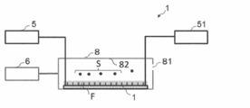
- FIG. 2 is a diagram showing an example of an embodiment of the device 1 of the present invention.
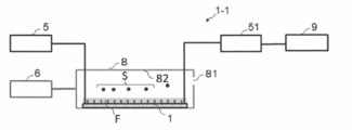
- FIG. 3 is a diagram showing an outline of the analyzer 1-1 of the present invention.
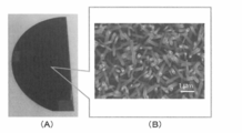
- 4A is a drawing-substituting photograph, which is a photograph of the device 1 produced in Example 1.
- FIG. FIG. 4B is a drawing-substituting photograph, which is an SEM image in which the surface of the device 1 is magnified 15,000 times.
- 5 (A) to 5 (D) are photographs substituted for drawings, a scanning transmission electron microscope of the nanowire of the device 1 manufactured in Example 1, and FIG.
- FIG. 5 (E) is an arrow direction in FIGS. 5 (C) and (D). It is a graph showing the intensity
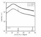
- FIG. 6 is a graph showing the X-ray diffraction measurement results of the glass substrate formed in Reference Example 1 on which the TiO 2 layer is formed.
- FIG. 7 is a graph showing the measurement results of the contact angle of the device 1 of Example 1 and Comparative Example 1.
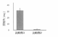
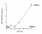
- FIG. 8 is a graph showing the measurement results of the contact angles of the glass substrates of Comparative Examples 2 and 3.
- FIG. 9A is a graph showing the change over time of the device produced in Example 1
- FIG. 9B is the graph showing the change over time of the glass substrate produced in Comparative Example 2.
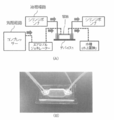
- FIG. 10A is a diagram showing an outline of the experimental apparatus manufactured in Example 2.
- FIG. 10B is a drawing substitute photograph, which is a photograph of the device 1 portion.
- FIG. 11A is a drawing substitute photograph, which is an SEM photograph of the surface of the device 1 and an enlarged photograph of the sample portion.
- FIG. 11B is a drawing-substituting photograph, which is an SEM photograph of the waste liquid obtained by centrifuging the liquid discharged by the liquid discharge mechanism and an enlarged photograph of the sample portion.
- FIG. 12 shows the results of analyzing the nanowires of the devices fabricated in Comparative Examples 4 and 5 and Example 3.
- the upper (A) is a drawing substitute photo, STEM image of nanowire
- the middle (B) is a drawing substitute photo, element mapping image by STEM-EDS
- the lower (C) is the characteristic X-ray intensity of Zn and Ti. It is a graph to represent.
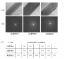
- FIG. 13 shows the results of analyzing the nanowires of the devices fabricated in Comparative Examples 4 and 5 and Example 3.
- the upper (A) is a drawing-substituting photograph, a TEM image of the nanowire
- the lower (B) is a drawing-substituting photograph, which is a limited-field electron diffraction pattern.
- (C) represents the surface interval measured from the diffraction pattern.
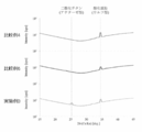
- FIG. 14 is a diagram showing the measurement results of the crystal structure of the nanowires of the devices fabricated in Comparative Examples 4 and 5 and Example 3.
- FIG. 15 is a graph showing changes over time of the device produced in Example 3 and the glass substrate produced in Comparative Example 2.
- FIG. 16 is a photograph substituted for a drawing
- FIG. 16A is a photograph of the device used in Example 4
- FIG. 16B is a photograph taken from the side of the device.
- FIG. 17B is a drawing-substituting photograph, and an SEM photograph of a sample directly collected by a filter.
- the sample collection device of the present invention (hereinafter sometimes simply referred to as “device”), an analysis apparatus including the device, and a device manufacturing method will be described in detail.
- FIG. 1A is a diagram for explaining the outline of the device 1 of the present invention.
- the device 1 of the present invention includes a substrate 2 and nanowires 3 formed on the substrate 2.
- FIG. 1B is a cross-sectional view of the nanowire 3, and the nanowire 3 includes a core nanowire 31 and a coat layer 32 formed on the outer periphery of the core nanowire 31.
- the coat layer 32 is formed of titanium dioxide having an anatase crystal structure. Therefore, since the surface of the nanowire 3 formed on the substrate 2 becomes superhydrophilic, the solution dropletized on the surface of the device 1 does not become a water droplet but forms a water film F spreading in a thin film shape.
- the substrate 2 is not particularly limited as long as the nanowire 3 can be formed and can withstand the temperature at the time of film formation using an atomic layer deposition apparatus described later, and examples thereof include glass and silicon.
- the core nanowire 31 formed on the substrate 2 may be produced by a known method.
- the core nanowire 31 may be grown by a known method by applying nanowire-forming particles or a catalyst.
- the nanowire-forming particles include ZnO.
- Nanowires using ZnO can be manufactured using a hydrothermal synthesis method. Specifically, first, ZnO is applied on the substrate 2. Next, the heated substrate 2 is immersed in a precursor solution in which zinc nitrate hexahydrate (Zn (NO 3 ) 2 .6H 2 O) and hexamethylenetetramine (C 6 H 12 N 4 ) are dissolved in deionized water. By doing so, ZnO nanowires can be grown. Note that the thickness of the core nanowire 31 can be changed by changing the concentration of the precursor solution.
- Examples of the catalyst for producing the core nanowire 31 include gold, platinum, aluminum, copper, iron, cobalt, silver, tin, indium, zinc, gallium, chromium, and titanium.
- a nanowire using a catalyst can be produced by the following procedure.
- a catalyst is deposited on the substrate 2.
- B) SiO 2, Li 2 O, MgO, Al 2 O 3, CaO, TiO 2, Mn 2 O 3, Fe 2 O 3, CoO, NiO, CuO, ZnO, Ga 2 O 3, SrO, In 2 O 3 , SnO 2 , Sm 2 O 3 , EuO or the like is used to form the core nanowire 31 by physical vapor deposition such as pulse laser deposition or VLS (Vapor-Liquid-Solid).
- the core nanowire 31 produced using a catalyst may be a nanowire having no branched chain or a nanowire having a branched chain.
- the coat layer 32 it is desirable to form a TiO 2 layer by vapor deposition using an atomic layer deposition (ALD apparatus) after forming the core nanowire 31.
- ALD apparatus atomic layer deposition
- the thickness of the coat layer 32 can be adjusted at the atomic level.
- the TiO 2 coat layer 32 may be made of a precursor that becomes TiO 2 after lamination, and examples thereof include tetrakis (diethylamino) titanium (TDMAT: Tetrakis (diethylamido) titanium), TiCl 4 and the like.
- the TiO 2 layer formed using the ALD apparatus is amorphous.
- TiO 2 can be converted into an anatase crystal structure.
- the heating temperature and time are not particularly limited as long as it can be converted into an anatase crystal structure.
- the heating may be performed at 300 to 500 ° C. for about 3 hours.
- the “titanium dioxide having an anatase crystal structure” may partially include other crystal structures such as an amorphous part and rutile as long as the effects of the present invention are not impaired.
- FIG. 2 is a diagram showing an example of an embodiment of the device 1 of the present invention.
- the device 1 of the present invention may be provided with a liquid supply mechanism 5 and / or an air supply mechanism 6 as necessary.
- the device 1 of the present invention can take the sample S in the atmosphere into the water film F by forming the water film F on the surface of the substrate 2.
- the analysis of the sample S taken into the water film F may be performed by putting the liquid on the device 1 into the analysis unit of the analyzer, but the analysis is preferably automated. Therefore, the device 1 may be provided with a liquid supply mechanism 5 that can supply a liquid at a predetermined supply amount to the surface of the device 1 where the nanowires 3 are formed.
- the liquid supply mechanism 5 is not particularly limited as long as the liquid can be supplied, and a known pump or the like may be used.
- the liquid is not particularly limited as long as it is an aqueous liquid.
- a conductive liquid is preferable when the liquid into which the sample S is taken is electrically analyzed. Examples of the conductive liquid include water, TE buffer, PBS buffer, HEPES buffer, and KCl aqueous solution.
- a liquid discharge mechanism 51 may be provided so that substantially the same amount of liquid as that supplied from the liquid supply mechanism 5 can be discharged.
- the liquid discharge mechanism 51 is not particularly limited as long as the liquid can be discharged, and a known pump or the like may be used.
- the air supply mechanism 6 is not essential. It may be provided when it is necessary to increase the contact between the surface of the device 1 and air.
- the air supply mechanism 6 is not particularly limited as long as it can send air. A small device such as a fan is desirable, but a known device such as a compressor may be used if necessary.
- the container 8 may be formed with a hole 81 for allowing the air supplied by the air supply mechanism 6 to escape to the outside. When the air discharged from the container 8 is reused, a tube or the like may be connected to the hole 81 to collect the discharged air. In the embodiment shown in FIG.
- the surface 82 of the container 8 that opposes the water film F is a flat surface, but the sample S contained in the air introduced into the container 8 can easily contact the water film F.
- the surface 82 may have a shape other than a plane. For example, by making the shape of a substantially triangular shape having an inclined surface such that the center of the surface 82 is close to the water film F, the air that has flowed into the container 8 flows toward the water film F along the inclined surface. Also good.
- FIG. 3 is a diagram showing an outline of the analyzer 1-1 of the present invention.
- the analysis apparatus 1-1 of the present invention includes at least the device 1 and the analysis unit 9 of the present invention.
- the analysis unit 9 is not particularly limited as long as it can analyze fine particles.
- an analyzer that measures changes in steady-state current that flows through pores (micropores) formed on a substrate such as silicon and that passes through the pores by a voltage applied to the pores. , Lab on a Chip, Vol. 12, pp. 2345-2352, 2012) or an analyzer (Naoya. Y et al. , “Tracking single-particle dynamics via combined optical and electrical sensing”, SCIENTIFIC REPORTS, Vol. 3, pp. 1-7, 2013, etc.).
- the device 1 of the present invention can be used as a sample collecting device for collecting PM2.5 or the like in the atmosphere, but may be used for other purposes.
- a water film can be formed on the board
- it can use for the filter etc. of an air cleaner, for example.
- the device of the present invention has very high durability (maintaining superhydrophilic performance), and titanium dioxide has a photocatalytic function. Therefore, application to purification of solutions containing outer walls and organic substances can be expected.
- Device 1 was produced by the following procedure. (1) Zinc oxide (ZnO) was laminated on a glass substrate (Slide glass S1112 manufactured by Matsunami Glass Industrial Co., Ltd.). For the lamination, an ALD apparatus (Savannah G2, manufactured by Cambridge Nanotech, the same applies below), diethyl zinc (DEZ; diethylzinc) as a precursor, H 2 O as a second precursor, 100 ° C., 15 cycles It laminated
- ALD apparatus Sivannah G2, manufactured by Cambridge Nanotech, the same applies below
- DEZ diethyl zinc
- H 2 O as a second precursor
- the device 1 of the present invention was manufactured by heating at 500 ° C. for 3 hours.
- FIG. 4A is a photograph of the device 1 produced in Example 1
- FIG. 4B is an SEM image in which the surface of the device 1 is magnified 15,000 times. As shown in FIG. 4B, it was confirmed that a large number of nanowires were formed on the surface of the substrate.
- Example 1 the device 1 manufactured in Example 1 was irradiated with ultrasonic waves, one nanowire was peeled from the substrate, and the distribution of Zn and Ti atoms in the nanowire was examined using a scanning transmission electron microscope (STEM). It was. STEM uses a JSMOL JSM-7610F (Schottky field emission scanning electron microscope; FESEM) with a STEM function and an energy dispersive X-ray analyzer (EDS), 30 kV EDS 100 cycles, STEM mode. Observed with.
- FIGS. 5A and 5B are photographs enlarged 30,000 times, and it was confirmed that Zn (Photo A) and Ti (Photo B) atoms were contained from the tip to the base of the nanowire.
- FESEM Schottky field emission scanning electron microscope
- EDS energy dispersive X-ray analyzer
- FIG. 5E is a graph showing the intensity of the characteristic X-rays of Zn and Ti at the distances in the directions of the arrows in FIGS.
- the strength of Zn becomes stronger (the amount of atoms is larger) as it is closer to the center of the nanowire.
- the amount of Ti was small at the end of the nanowire, no significant change was observed near the center. From the above results, it was confirmed that Ti was coated on the outer periphery of the nanowire.
- tetrakis (diethylamino) titanium (TDMAT) is used as a precursor, H 2 O is used as a second precursor, and a TiO 2 layer is formed on a glass substrate under conditions of 100 ° C. and 600 cycles. did. Subsequently, it heated at 500 degreeC for 3 hours. For comparison, a glass substrate that was not heated after laminating TiO 2 was also prepared. Next, the crystal structure of TiO 2 on the glass substrate was measured using an X-ray diffractometer (ATX-G manufactured by Rigaku Corporation). FIG.
- FIG. 6 is a diagram showing the measurement results, where “after” indicates the measurement result of the crystal structure of the TiO 2 layer after heating and “before” indicates the measurement result of the crystal structure of the TiO 2 layer before heating.
- 2 ⁇ (Cu K ⁇ ) / degree value of J. Am. Ceram. Soc., 1996, 79, 1095-1099
- anatase which is a crystal structure of TiO 2 . Etc.
- no peak was observed around 25.5 which is the value of 2 ⁇ (Cu K ⁇ ) / degree of anatase, but in “after” after heating, as shown by the arrow, the anatase crystal structure A peak was observed.
- FIG. 7 is a graph showing the measurement results of the contact angle of the device 1 of Example 1 and Comparative Example 1.
- the contact angle of the device 1 of Example 1 was 0 degree.
- the contact angle of the device 1 that was not heated was about 15 degrees.
- FIG. 8 is a graph showing the measurement results of the contact angles of the glass substrates of Comparative Examples 2 and 3. Although the contact angle of the glass substrate laminated with TiO 2 was reduced by the heat treatment, the contact angle did not reach 0 degrees.
- FIG. 9A is a graph showing the change over time of the device 1 produced in Example 1
- FIG. 9B is the graph showing the change over time of the glass substrate produced in Comparative Example 2.
- the glass substrate heat-treated by laminating TiO 2 of Comparative Example 2 showed a relatively low contact angle until about 6 days after the heat treatment, but the contact angle suddenly increased after 6 days.
- the device 1 of Example 1 surprisingly had a contact angle of 0 even after 30 days, just after the heat treatment. Therefore, since the device 1 of the present invention can form a water film on the surface of the device 1 over a long period of time, it is useful as a sample collection device.
- FIG. 10A is a diagram showing an outline of the experimental apparatus
- FIG. 10B is a photograph of the device 1 portion of the experimental apparatus.
- the experimental apparatus was produced by the following procedure. (1) A container produced by PDMS was placed on the device 1 produced in Example 1. (2) A tube (PEEK tube: diameter 0.5 mm, two thin tubes in FIG. 10B) connected to a syringe pump as a liquid supply mechanism and a liquid discharge mechanism is inserted into the hole formed on the upper surface of the container. Connected. (3) A tube (PTFE tube: diameter 1.53 mm, thick tube in FIG.
- a tube (PTFE tube: diameter 1.53 mm, thick tube in FIG. 10B) that discharges air sent from the compressor was connected to the hole formed on the upper surface of the container. The other end of the tube was positioned in the water bath.
- a sample collection experiment was performed according to the following procedure.
- a water film was formed on the surface of the device 1 by sending water from the syringe pump (liquid supply mechanism) of the fabricated experimental apparatus to the surface of the device 1.
- the same amount of water as the supply amount was discharged from the device 1 using a syringe pump (liquid discharge mechanism).
- Use urban atmospheric dust No. 28 obtained from the National Institute for Environmental Studies as a sample, adjust the air containing dust with an aerosol generator, then send the adjusted air to the container, and remove the water film and dust from the device 1 The contained air was in contact. After a predetermined time, the device 1 was taken out and dried, and the substrate surface was observed with an SEM.
- FIG. 11A is an SEM photograph of the surface of the device 1 and an enlarged photograph of the sample portion.
- FIG. 11B is an SEM photograph of the waste liquid obtained by centrifuging the liquid discharged by the liquid discharge mechanism for 5,000 rcf for 10 minutes, and an enlarged photograph of the sample portion.
- fine particles such as PM2.5 in the atmosphere could be collected by using the device 1 of the present invention.
- the liquid containing the fine particles collected from the device 1 can be collected, the sample can be continuously analyzed.
- Example 3 [Production of Device 1] ⁇ Example 3> (5) in Example 1 (5) 100 ° C., 100 cycles, (6) 500 ° C. for 3 hours, (5) 100 ° C., 200 cycles, (6) 350 ° C., 3 hours, A device 1 was produced in the same procedure as in Example 1 except that. Further, in the same procedure as in Example 1, one nanowire was peeled from the manufactured device 1 and a STEM image was taken, and the distribution of Zn and Ti atoms in the nanowire was examined.
- Example 3 Comparative Example a device which did not form a coating layer of titanium dioxide (TiO 2) 4, as coating layer in Comparative Example 5 The device was but was not heat-treated to form the titanium dioxide (TiO 2) did. Next, as in Example 3, an STEM image was taken and the distribution of Zn and Ti atoms in the nanowire was examined.
- FIG. 12 shows nanowires of the devices manufactured in Comparative Examples 4 and 5 and Example 3.
- the upper (A) is the STEM image of the nanowire
- the middle (B) is the element mapping image by STEM-EDS
- the lower (C) Is a graph showing the intensity of characteristic X-rays of Zn and Ti. As is clear from FIG. 12, it was confirmed that TiO 2 was coated on the outer periphery of the nanowires of the devices fabricated in Example 3 and Comparative Example 5.
- Example 3 and Comparative Example 5 have a core-shell structure from the contrast.
- the spacing between the nanowires of Example 3 was changed by heating the nanowires of Comparative Example 5.
- the value of the face spacing in Example 3 was the same as the face spacing exhibited by the anatase crystal structure.
- the anatase crystal structure shows the spacing between the databases of the National Institute for Materials Science (MatNavi) (zinc oxide_wurtzite: http://crystdb.nims.go.jp/crystdb/search-details ?
- FIG. 14 shows the measurement results. Since only the nanowire of Example 3 had a peak around 25.5 which is the value of 2 ⁇ (Cu K ⁇ ) / degree of anatase, the titanium dioxide (TiO 2 ) around the nanowire of the device of Example 3 It was confirmed that the coat layer had an anatase crystal structure.
- FIG. 15 shows the results of the measured change over time.
- [Measurement of change in contact angle with time] in Example 1 only 30 days were measured.
- the contact angle was 0 as in the case immediately after the heat treatment. From the above results, the device of the present invention can form a water film over a long period of time.
- Example 4 Next, in the sample collection experiment of Example 2, the device of Example 3 was used instead of the device of Example 1, and the container of Example 2 was replaced, and the center of the container surface facing the water film was the water film.
- An experimental apparatus was produced in the same procedure as in Example 2 except that a container having a shape having an inclined surface that was close to the surface was used.
- FIG. 16A is a photograph of the device used in Example 4, and FIG. 16B is a photograph from the side of the device. A portion surrounded by white in FIG. 16B is a space through which ventilation and water pass in the device.
- the air flowing into the container from the air supply mechanism was formed to flow in the water film direction.
- a collection experiment was performed by introducing an aerosol in which a dust sample similar to that in Example 2 was dispersed into a test apparatus from a tube.
- the liquid discharged by the liquid discharge mechanism was passed through a filter (pore diameter 0.1 ⁇ m: polycarbonate track-etched membrane filter manufactured by Merck), and dust in the discharged liquid was sampled on the filter.
- dust was sampled on the filter by suspending the dust in pure water and passing the suspension through a similar filter.
- FIG. 17B is a SEM photograph of a sample directly collected by a filter
- FIG. 17D is a SEM photograph of the sample contained in the liquid discharged by the liquid discharge mechanism
- the size distributions of both were substantially the same. From the above results, it was revealed that the device produced in Example 3 can collect the sample regardless of the particle size of the sample contained in the air. Therefore, since the device produced in Example 3 can accurately measure the proportion of dust of various sizes contained in the atmosphere, it is useful for continuous monitoring of dust in the atmosphere.
- the sample collection device of the present invention can form a water film on the surface, it can collect a minute sample floating in the atmosphere over the entire surface of the device. Moreover, since a water film can be formed over a long period of time, the function as a sample collection device can be maintained over a long period of time. Therefore, it is useful for the analyzer industry.
Landscapes
- Health & Medical Sciences (AREA)
- Life Sciences & Earth Sciences (AREA)
- Biochemistry (AREA)
- General Health & Medical Sciences (AREA)
- Molecular Biology (AREA)
- Physics & Mathematics (AREA)
- Chemical & Material Sciences (AREA)
- Analytical Chemistry (AREA)
- Engineering & Computer Science (AREA)
- Biomedical Technology (AREA)
- General Physics & Mathematics (AREA)
- Immunology (AREA)
- Pathology (AREA)
- Sampling And Sample Adjustment (AREA)
- Separation Of Particles Using Liquids (AREA)
- Inorganic Compounds Of Heavy Metals (AREA)
- Catalysts (AREA)
Abstract
大気中の浮遊粒子を捕集できるサンプル捕集デバイスを提供することを課題とする。基板、該基板上に形成されたナノワイヤを含み、前記ナノワイヤは、コアナノワイヤ及び該コアナノワイヤの外周に形成されたコート層を含み、前記コート層は、アナターゼ結晶構造を有する二酸化チタンである、大気中のサンプル捕集デバイスを提供することで、課題が解決する。
Description
本発明は、サンプル捕集デバイス、サンプル捕集デバイスを含む分析装置、及びサンプル捕集デバイスの製造方法に関する。特に、サンプル捕集デバイスが、アナターゼ結晶構造を有する二酸化チタンのコート層を形成したナノワイヤを表面に有することで超親水性になり、そして、サンプル捕集デバイスの表面に水フィルムを形成することで、空気中を浮遊している微小サンプルを捕集できるサンプル捕集デバイス、サンプル捕集デバイスを含む分析装置、及びサンプル捕集デバイスの製造方法に関する。
大気中に浮遊するPM2.5、ウィルス、花粉、菌、毒素等の有害・危険物質は、ヒトなどの生体の健康状態に影響を与える可能性が指摘されている。そのため、ヒトが安全で快適な生活を送るために、大気中のこれら有害・危険物質を正確に分析する必要がある。
例えば、PM2.5を分析する装置・方法としては、フィルタに捕集したPM2.5をX線蛍光分析法により測定する方法が知られている(特許文献1参照)。
また、大気に含まれる粒子を測定する他の方法としては、測定粒子と反応する薬が含浸又は塗布されているフィルタを通して大気を吸引し、フィルタが測定粒子を捕集した後も大気を吸引し続けて、大気中の水分によって測定粒子を湿らせることで薬と反応させて固定する粒子捕集方法が知られている(特許文献2参照)。
身の回りの有害・危険物質(サンプル)を誰もが簡単に測定するためには、装置全体を小型化、簡素化する必要がある。しかしながら、特許文献1及び2に記載されている発明は、何れも大気中のサンプルを吸引手段で吸引してフィルタに捕集している。そのため、吸引手段及び吸引手段を駆動するための電源等が必要となり、装置が大型化するという問題がある。
近年、基板上に形成した微細な孔や流路を微粒子が通過する時のイオン電流の変化を測定することで、微粒子の大きさ等を検出する分析方法の開発が進められている。当該分析方法は、溶液に含まれる微粒子が電気泳動等により、微細な孔や流路を通過すればよいことから、装置を小型化できる。そのため、大気中のサンプル分析装置への適用が期待されている。
ところで、当該分析方法により大気中のサンプルを測定する場合、溶液に大気中のサンプルを捕集する必要がある。大気中のサンプルを溶液に捕集する為には、例えば、コンプレッサー等を用い、大気を溶液中でバブリングする方法等が考えられる。しかしながら、大気を溶液中でバブリングするためには、装置が大型化するという問題がある。分析装置を小型化するためには、大気中のサンプルを捕集するためのデバイスも小型化する必要がある。しかしながら、現状では大気中のサンプルを溶液に捕集できる小型デバイスは知られていない。
本発明は、上記従来の問題を解決するためになされた発明であり、鋭意研究を行ったところ、(1)アナターゼ結晶構造を有する二酸化チタンでコート層を形成したナノワイヤを基板表面に形成すると基板表面が超親水性になること、(2)基板表面が超親水性になることから基板上に滴下した溶液の接触角はほぼゼロになること、(3)接触角がほぼゼロとなることから、基板上に滴下した溶液は水滴にならずに薄膜状(水フィルム)に広がるため、基板の全表面で大気中のサンプルと接触できること、(4)アナターゼ結晶構造を有する二酸化チタンでコート層を形成したナノワイヤを基板表面に形成すると、超親水性能が長期間にわたり維持できること、を新たに見出した。
本発明は、以下に示す、サンプル捕集デバイス、サンプル捕集デバイスを含む分析装置、及びサンプル捕集デバイスの製造方法に関する。
(1)基板、該基板上に形成されたナノワイヤを含み、
前記ナノワイヤは、コアナノワイヤ及び該コアナノワイヤの外周に形成されたコート層を含み、
前記コート層は、アナターゼ結晶構造を有する二酸化チタンである、
サンプル捕集デバイス。
(2)前記基板に液体を供給する液体供給機構、
を少なくとも含む、上記(1)に記載のサンプル捕集デバイス。
(3)前記基板に空気を供給する空気供給機構、
を含む、上記(1)又は(2)に記載のサンプル捕集デバイス。
(4)上記(1)~(3)の何れか一に記載のサンプル捕集デバイス、
分析部、
を含む分析装置。
(5)基板上にコアナノワイヤを形成する工程、
形成したナノワイヤの外周に、二酸化チタンのコート層を形成する工程、
加熱によりアモルファス状の二酸化チタンをアナターゼ結晶構造に変換する加熱工程、
を含む、サンプル捕集デバイスの製造方法。
前記ナノワイヤは、コアナノワイヤ及び該コアナノワイヤの外周に形成されたコート層を含み、
前記コート層は、アナターゼ結晶構造を有する二酸化チタンである、
サンプル捕集デバイス。
(2)前記基板に液体を供給する液体供給機構、
を少なくとも含む、上記(1)に記載のサンプル捕集デバイス。
(3)前記基板に空気を供給する空気供給機構、
を含む、上記(1)又は(2)に記載のサンプル捕集デバイス。
(4)上記(1)~(3)の何れか一に記載のサンプル捕集デバイス、
分析部、
を含む分析装置。
(5)基板上にコアナノワイヤを形成する工程、
形成したナノワイヤの外周に、二酸化チタンのコート層を形成する工程、
加熱によりアモルファス状の二酸化チタンをアナターゼ結晶構造に変換する加熱工程、
を含む、サンプル捕集デバイスの製造方法。
本発明のサンプル捕集デバイスに滴下した溶液は、水滴にならずに薄膜状に広がる。そのため、サンプル捕集デバイスの全表面で大気中のサンプルを捕集できる。また、本発明のサンプル捕集デバイスは、二酸化チタンで表面処理したガラス等の基板と比較して、超親水性能を長期間にわたり維持できる。したがって、長期間に渡りサンプル捕集デバイスとしての機能を維持できる。
以下に、本発明のサンプル捕集デバイス(以下、単に「デバイス」と記載することがある。)、デバイスを含む分析装置、及びデバイスの製造方法について詳しく説明する。
図1(A)は、本発明のデバイス1の概略を説明するための図である。本発明のデバイス1は、基板2、基板2上に形成されたナノワイヤ3を含んでいる。図1(B)は、ナノワイヤ3の断面図であり、ナノワイヤ3は、コアナノワイヤ31及びコアナノワイヤ31の外周に形成されたコート層32を含んでいる。コート層32は、アナターゼ結晶構造を有する二酸化チタンで形成されている。そのため、基板2に形成したナノワイヤ3の表面は超親水性となることから、デバイス1の表面に滴化した溶液は水滴にはならずに、薄膜状に広がった水フィルムFを形成する。
基板2は、ナノワイヤ3が形成でき、且つ後述する原子層堆積装置を用いた製膜時の温度に耐えられるものであれば特に制限は無く、ガラス、シリコン等が挙げられる。
基板2上に形成するコアナノワイヤ31は、公知の方法により作製すればよく、例えば、ナノワイヤ形成用粒子又は触媒を塗布し公知の方法でコアナノワイヤ31を成長させればよい。ナノワイヤ形成用粒子としては、例えば、ZnOが挙げられる。ZnOを用いたナノワイヤは、水熱合成方法を用いて作製することができる。具体的には、先ず、ZnOを基板2上に塗布する。次いで、硝酸亜鉛六水和物(Zn(NO3)2・6H2O)、ヘキサメチレンテトラミン(C6H12N4)を脱イオン水に溶解した前駆体溶液に、加熱した基板2を浸漬させることで、ZnOナノワイヤを成長させることができる。なお、前駆体溶液の濃度を変えると、コアナノワイヤ31の太さを変えることができる。
コアナノワイヤ31作製用の触媒としては、例えば、金、プラチナ、アルミニウム、銅、鉄、コバルト、銀、錫、インジウム、亜鉛、ガリウム、クロム、チタン等が挙げられる。触媒を用いたナノワイヤは、次の手順で作製することができる。
(a)触媒を基板2上に堆積する。
(b)SiO2、Li2O、MgO、Al2O3、CaO、TiO2、Mn2O3、Fe2O3、CoO、NiO、CuO、ZnO、Ga2O3、SrO、In2O3、SnO2、Sm2O3、EuO等の材料を用い、パルスレーザーデポジション、VLS(Vapor-Liquid-Solid)法等の物理蒸着法でコアナノワイヤ31を形成する。なお、触媒を用いて作製するコアナノワイヤ31は、分岐鎖を有しないナノワイヤであってもよいし、分岐鎖を有するナノワイヤであってもよい。
(a)触媒を基板2上に堆積する。
(b)SiO2、Li2O、MgO、Al2O3、CaO、TiO2、Mn2O3、Fe2O3、CoO、NiO、CuO、ZnO、Ga2O3、SrO、In2O3、SnO2、Sm2O3、EuO等の材料を用い、パルスレーザーデポジション、VLS(Vapor-Liquid-Solid)法等の物理蒸着法でコアナノワイヤ31を形成する。なお、触媒を用いて作製するコアナノワイヤ31は、分岐鎖を有しないナノワイヤであってもよいし、分岐鎖を有するナノワイヤであってもよい。
コート層32は、コアナノワイヤ31を形成後、原子層堆積装置(ALD装置:Atomic Layer Deposition)を用いた蒸着法によりTiO2層を形成することが望ましい。ALD装置を用いると、コート層32の厚さを原子レベルで調整することができる。TiO2のコート層32は、積層後にTiO2となる前駆体を用いればよく、例えば、テトラキス(ジエチルアミノ)チタン(TDMAT:Tetrakis(diethylamido)titanium)、TiCl4等が挙げられる。
ALD装置を用いて形成したTiO2層は、アモルファス状である。所定温度及び時間で加熱することで、TiO2をアナターゼ結晶構造に変換することができる。加熱温度及び時間は、アナターゼ結晶構造に変換できれば特に制限は無く、例えば、300~500℃で3時間程度、加熱すればよい。なお、「アナターゼ結晶構造を有する二酸化チタン」は、本発明の効果を損なわない範囲内であれば、アモルファス部分やルチル等の他の結晶構造が一部含まれていても良い。
図2は、本発明のデバイス1の実施形態の一例を示す図である。本発明のデバイス1には、必要に応じて、液体供給機構5及び/又は空気供給機構6を設けてもよい。本発明のデバイス1は、基板2の表面に水フィルムFを形成することで、大気中のサンプルSを水フィルムFに取り込むことができる。水フィルムFに取り込んだサンプルSの分析は、デバイス1上の液体を分析装置の分析部に投入すればよいが、分析は自動化することが好ましい。そのため、デバイス1のナノワイヤ3が形成されている表面に液体を所期の供給量で供給できる液体供給機構5をデバイス1に設けてもよい。液体供給機構5は、液体が供給できれば特に制限は無く、公知のポンプ等を用いればよい。なお、液体は水性の液体であれば特に制限はないが、後述するとおり、サンプルSを取り込んだ液体を電気的に分析する場合は導電性の液体が好ましい。導電性の液体としては、例えば、水、TEバッファー、PBSバッファー、HEPESバッファー、KCl水溶液等が挙げられる。
デバイス1の表面は超親水性であることから、基板2上に排出流路や孔を形成、又は基板に傾斜をつけることで、サンプルSを取り込んだ液体がデバイス1から流れ出て、分析装置の分析部に到達するようにすればよい。また、液体排出機構51を設け、液体供給機構5から供給した液体とほぼ同量の液体を排出できるようにしてもよい。液体排出機構51を設けた場合は、分析部に送るサンプルSを取り込んだ液体の量が一定になるので、定量分析をすることもできる。液体排出機構51は、液体を排出できれば特に制限は無く、公知のポンプ等を用いればよい。
空気供給機構6は必須ではない。デバイス1の表面と空気の接触を増加する必要がある場合に設ければよい。空気供給機構6は、空気を送ることができれば特に制限はない。ファン等の小型の装置が望ましいが、必要に応じてコンプレッサー等の公知の装置を用いればよい。なお、空気供給機構6を設ける場合は、必要に応じて、少なくともデバイス1の水フィルムを形成する部分を覆うことができる容器8を設けてもよい。また、容器8には、空気供給機構6で供給した空気を外部に逃がすための孔81を形成してもよい。なお、容器8から排出した空気を再利用する場合は、孔81にチューブ等を接続し、排出した空気を回収してもよい。また、図2に示す実施形態では、容器8の水フィルムFに対抗する面82は平面であるが、容器8内に導入した空気中に含まれるサンプルSが水フィルムFに接触し易くするために面82を平面以外の形状にしてもよい。例えば、面82の中央が水フィルムFに近接するような傾斜面を持つ略三角形等の形状とすることで、容器8内に流入した空気を傾斜面に沿って水フィルムFに向かうよう流してもよい。
図3は、本発明の分析装置1-1の概略を示す図である。本発明の分析装置1-1は、本発明のデバイス1と分析部9を少なくとも含んでいる。分析部9としては、微粒子を分析できるものであれば特に制限はない。例えば、シリコン等の基板上に形成した細孔(マイクロポア)にサンプルを通過させ、細孔に印加した電圧によって細孔の内部を流れる定常電流の変化を測定する分析装置(Waseem A.et al.,Lab on a Chip, Vol.12, pp.2345-2352,2012,参照。)や、マイクロ流路を形成した基板を横置きにし、定常電流を測定する分析装置(Naoya.Y et al.,“Tracking single-particle dynamics via combined optical and electrical sensing”, SCIENTIFIC REPORTS, Vol.3, pp.1-7,2013,参照。)等が挙げられる。
上記のとおり、本発明のデバイス1は大気中のPM2.5等を捕集するサンプル捕集デバイスとして用いることができるが、その他の用途に用いてもよい。例えば、基板2上に水フィルムを形成できることから、例えば、空気清浄器のフィルタ等に用いることができる。また、本発明のデバイスは、耐久性(超親水性能の維持)が非常に高く、また、二酸化チタンは光触媒の機能を有する。したがって、外壁や有機物を含んだ溶液の浄化等への応用も期待できる。
以下に実施例を掲げ、本発明を具体的に説明するが、この実施例は単に本発明の説明のため、その具体的な態様の参考のために提供されているものである。これらの例示は本発明の特定の具体的な態様を説明するためのものであるが、本願で開示する発明の範囲を限定したり、あるいは制限することを表すものではない。
[デバイス1の作製]
<実施例1>
以下の手順によりデバイス1を作製した。
(1)ガラス基板(松波硝子工業株式会社製スライドガラスS1112)上に、酸化亜鉛(ZnO)を積層した。積層には、ALD装置(Cambridge Nanotech社製Savannah G2、以下も同様。)、前駆体にはジエチル亜鉛(DEZ;diethylzinc)、第2前駆体にはH2Oを用い、100℃、15サイクルの条件で積層した。
(2)50mLビーカーにヘキサメチレンテトラミン0.225gと、硝酸亜鉛6水和物0.476gを入れて撹拌し、ナノワイヤ成長液を作製した。
(3)上記(1)でZnOを積層したガラス基板を、上記(2)で作製したナノワイヤ成長液に浸漬した。
(4)ナノワイヤ成長液のビーカーの天井部をラップで多い、オーブンの中に入れ、95℃、3時間加熱することで、ガラス基板上にZnOからなるコアナノワイヤを作製した。
(5)上記(4)で作製したコアナノワイヤの周囲に二酸化チタン(TiO2)のコート層を形成した。コート層は、ALD装置、前駆体にはテトラキス(ジエチルアミノ)チタン(TDMAT)、第2前駆体にはH2Oを用い、100℃、100サイクルの条件で形成した。
(6)次いで、500℃で3時間加熱し、本発明のデバイス1を作製した。
<実施例1>
以下の手順によりデバイス1を作製した。
(1)ガラス基板(松波硝子工業株式会社製スライドガラスS1112)上に、酸化亜鉛(ZnO)を積層した。積層には、ALD装置(Cambridge Nanotech社製Savannah G2、以下も同様。)、前駆体にはジエチル亜鉛(DEZ;diethylzinc)、第2前駆体にはH2Oを用い、100℃、15サイクルの条件で積層した。
(2)50mLビーカーにヘキサメチレンテトラミン0.225gと、硝酸亜鉛6水和物0.476gを入れて撹拌し、ナノワイヤ成長液を作製した。
(3)上記(1)でZnOを積層したガラス基板を、上記(2)で作製したナノワイヤ成長液に浸漬した。
(4)ナノワイヤ成長液のビーカーの天井部をラップで多い、オーブンの中に入れ、95℃、3時間加熱することで、ガラス基板上にZnOからなるコアナノワイヤを作製した。
(5)上記(4)で作製したコアナノワイヤの周囲に二酸化チタン(TiO2)のコート層を形成した。コート層は、ALD装置、前駆体にはテトラキス(ジエチルアミノ)チタン(TDMAT)、第2前駆体にはH2Oを用い、100℃、100サイクルの条件で形成した。
(6)次いで、500℃で3時間加熱し、本発明のデバイス1を作製した。
図4(A)は実施例1で作製したデバイス1の写真、図4(B)はデバイス1の表面を15、000倍に拡大したSEM画像である。図4(B)に示すように、基板の表面に多数のナノワイヤが形成されたことを確認した。
次に、実施例1で作製したデバイス1に超音波を照射し、基板からナノワイヤを1本剥離し、走査透過型電子顕微鏡(STEM)を用いて、ナノワイヤ中のZn及びTi原子の分布を調べた。STEMはJEOL社製JSM-7610F(ショットキー電界放出形走査電子顕微鏡;FESEM)に、STEM機能とエネルギー分散形X線分析装置(EDS)を付属させた装置を用い、30kV EDS 100サイクル、STEM modeで観察した。図5(A)及び(B)は30,000倍に拡大した写真で、ナノワイヤの先端から基部まで、Zn(写真A)及びTi(写真B)原子が含まれていることを確認した。次に、STEMを150,000倍に拡大し、図5(C)及び(D)に示す破線で囲まれているナノワイヤに電子線を当てた際に放出される、Zn及びTiの特性X線の強度を検出した。図5(E)は、図5(C)及び(D)の矢印方向の距離におけるZn及びTiの特性X線の強度を表すグラフである。図5(E)に示すように、Znはナノワイヤの中心に近い程強度が強く(原子の量が多い)なった。一方、Tiはナノワイヤの端部では量は少ないものの、中心付近では大きな変化は見られなかった。以上の結果より、Tiはナノワイヤの外周にコートされていることを確認した。
[アナターゼ結晶構造の確認]
<参考例1>
結晶構造は、X線回折装置を用いて調べることができる。先ず、参考例として、ガラス基板上にTiO2層を形成し、加熱の有無による結晶構造の変化を観察した。
<参考例1>
結晶構造は、X線回折装置を用いて調べることができる。先ず、参考例として、ガラス基板上にTiO2層を形成し、加熱の有無による結晶構造の変化を観察した。
具体的には、ALD装置、前駆体にはテトラキス(ジエチルアミノ)チタン(TDMAT)、第2前駆体にはH2Oを用い、100℃、600サイクルの条件でガラス基板上にTiO2層を形成した。次いで、500℃で3時間加熱した。なお、比較のため、TiO2を積層後、加熱しなかったガラス基板も準備した。次いで、X線回折装置(株式会社リガク社製ATX-G)を用いて、ガラス基板上のTiO2の結晶構造を測定した。図6は測定結果を示す図で、“after”は加熱後、“before”は加熱前のTiO2層の結晶構造の測定結果を表す。また、グラフの下には、TiO2の結晶構造であるアナターゼ(Anatase;鋭錐石)の2θ(Cu Kα)/degreeの値(J.Am.Ceram.Soc.,1996,79,1095-1099等)を併せて示す。加熱前の“before”ではアナターゼの2θ(Cu Kα)/degreeの値である25.5付近にピークは見られなかったが、加熱後の“after”では、矢印に示すようにアナターゼ結晶構造のピークが観察できた。以上の結果より、TiO2を積層後、加熱処理をすることでアナターゼ結晶構造のTiO2層が形成できることを確認した。
[デバイス1の濡れ性の確認]
次に、実施例1で作製したデバイス1の接触角を調べた。接触角は、協和界面科学株式会社製DM-501を用い、シリンジから0.5μLの液滴を作製して基板に着滴させ、1秒後の画像を取得した。取得画像より、θ/2法によって静的接触角の値を測るという手順で測定した。
次に、実施例1で作製したデバイス1の接触角を調べた。接触角は、協和界面科学株式会社製DM-501を用い、シリンジから0.5μLの液滴を作製して基板に着滴させ、1秒後の画像を取得した。取得画像より、θ/2法によって静的接触角の値を測るという手順で測定した。
<比較例1>
実施例1のデバイス1の作製において、(6)の加熱をしなかったものを比較例1のデバイス1とし、上記と同様の手順で濡れ性を確認した。
実施例1のデバイス1の作製において、(6)の加熱をしなかったものを比較例1のデバイス1とし、上記と同様の手順で濡れ性を確認した。
図7は、実施例1及び比較例1のデバイス1の接触角の測定結果を示すグラフである。実施例1のデバイス1の接触角は0度であった。一方、比較例1のTiO2のコート層を形成後、加熱しなかったデバイス1の接触角は約15度であった。
<比較例2、3>
ALD装置、前駆体にはテトラキス(ジエチルアミノ)チタン(TDMAT)、第2前駆体にはH2Oを用い、100℃、200サイクルの条件でガラス基板上にTiO2を積層した。次いで、TiO2を積層した後に、500℃で3時間加熱したガラス基板を比較例2、加熱しなかったガラス基板を比較例3とした。比較例1と同様の手順で、濡れ性を測定した。
ALD装置、前駆体にはテトラキス(ジエチルアミノ)チタン(TDMAT)、第2前駆体にはH2Oを用い、100℃、200サイクルの条件でガラス基板上にTiO2を積層した。次いで、TiO2を積層した後に、500℃で3時間加熱したガラス基板を比較例2、加熱しなかったガラス基板を比較例3とした。比較例1と同様の手順で、濡れ性を測定した。
図8は、比較例2及び3のガラス基板の接触角の測定結果を示すグラフである。加熱処理することで、TiO2を積層したガラス基板の接触角は小さくなるものの、接触角は0度までにはならなかった。
[接触角の経時変化の測定]
次に、実施例1で作製したデバイス1及び比較例2で作製したガラス基板の濡れ性の経時変化を確認した。図9(A)は実施例1で作製したデバイス1、図9(B)は比較例2で作製したガラス基板の経時変化を示すグラフである。比較例2のTiO2を積層して加熱処理したガラス基板は、加熱処理直後6日頃までは、比較的低い接触角を示していたが、6日以降は急激に接触角が大きくなった。一方、実施例1のデバイス1は、驚くべきことに、30日を経過した時点でも加熱処理直後と同様に接触角が0のままであった。したがって、本発明のデバイス1は、長期間にわたりデバイス1の表面に水フィルムを形成することができるので、サンプル捕集デバイスとして有用である。
次に、実施例1で作製したデバイス1及び比較例2で作製したガラス基板の濡れ性の経時変化を確認した。図9(A)は実施例1で作製したデバイス1、図9(B)は比較例2で作製したガラス基板の経時変化を示すグラフである。比較例2のTiO2を積層して加熱処理したガラス基板は、加熱処理直後6日頃までは、比較的低い接触角を示していたが、6日以降は急激に接触角が大きくなった。一方、実施例1のデバイス1は、驚くべきことに、30日を経過した時点でも加熱処理直後と同様に接触角が0のままであった。したがって、本発明のデバイス1は、長期間にわたりデバイス1の表面に水フィルムを形成することができるので、サンプル捕集デバイスとして有用である。
[サンプルの捕集実験]
<実施例2>
次に、実施例1のデバイス1を用いて空気中のサンプル捕集実験を行った。図10(A)は実験装置の概略を示す図で、図10(B)は実験装置のデバイス1部分の写真である。実験装置は、次の手順で作製した。
(1)実施例1で作製したデバイス1の上にPDMSで作製した容器を被せた。
(2)容器の上面に形成した孔に、液体供給機構及び液体排出機構であるシリンジポンプに接続するチューブ(PEEKチューブ:直径0.5mm、図10(B)中の細い2本のチューブ)を接続した。
(3)容器の上面に形成した孔に、空気供給機構であるコンプレッサーに接続するチューブ(PTFEチューブ:直径1.53mm、図10(B)中の太いチューブ)を接続した。なお、デバイス1とコンプレッサーの間には、エアロゾルジェネレーターを設けた。
(4)容器の上面に形成した孔に、コンプレッサーから送られた空気を排出するチューブ(PTFEチューブ:直径1.53mm、図10(B)中の太いチューブ)を接続した。チューブの他端は、水槽中に位置させた。
<実施例2>
次に、実施例1のデバイス1を用いて空気中のサンプル捕集実験を行った。図10(A)は実験装置の概略を示す図で、図10(B)は実験装置のデバイス1部分の写真である。実験装置は、次の手順で作製した。
(1)実施例1で作製したデバイス1の上にPDMSで作製した容器を被せた。
(2)容器の上面に形成した孔に、液体供給機構及び液体排出機構であるシリンジポンプに接続するチューブ(PEEKチューブ:直径0.5mm、図10(B)中の細い2本のチューブ)を接続した。
(3)容器の上面に形成した孔に、空気供給機構であるコンプレッサーに接続するチューブ(PTFEチューブ:直径1.53mm、図10(B)中の太いチューブ)を接続した。なお、デバイス1とコンプレッサーの間には、エアロゾルジェネレーターを設けた。
(4)容器の上面に形成した孔に、コンプレッサーから送られた空気を排出するチューブ(PTFEチューブ:直径1.53mm、図10(B)中の太いチューブ)を接続した。チューブの他端は、水槽中に位置させた。
次に、以下の手順でサンプルの捕集実験を行った。作製した実験装置のシリンジポンプ(液体供給機構)から、デバイス1の表面に水を送ることで、デバイス1の表面に水フィルムを形成した。また、シリンジポンプ(液体排出機構)を用い、供給量と同じ量の水をデバイス1から排出した。サンプルには国立環境研究所から入手した都市大気粉塵(No.28)を用い、エアロゾルジェネレーターで粉塵を含む空気を調整し、次いで、調整した空気を容器に送り、デバイス1の水フィルムと粉塵を含んだ空気が接触するようにした。所定時間経過後、デバイス1を取り出し、乾燥後、基板表面をSEMで観察した。図11(A)はデバイス1の表面のSEM写真及びサンプル部分を拡大した写真である。また、図11(B)は液体排出機構により排出した液体を5,000rcf、10分間遠心分離した廃液のSEM写真及びサンプル部分を拡大した写真である。
図11(A)の写真から明らかなように、本発明のデバイス1を用いることで、大気中のPM2.5等の微粒子を捕集することができた。また、デバイス1から捕集した微粒子を含む液体を回収できることから、引き続き、サンプルの分析をすることができる。
[デバイス1の作製]
<実施例3>
実施例1の(5)の100℃、100サイクルの条件、(6)の500℃で3時間加熱に代え、(5)100℃、200サイクルの条件、(6)350℃で3時間加熱、とした以外は実施例1と同様の手順で、デバイス1を作製した。また、実施例1と同様の手順で、作製したデバイス1からナノワイヤを1本剥離し、STEM画像を撮像するとともに、ナノワイヤ中のZn及びTi原子の分布を調べた。
<実施例3>
実施例1の(5)の100℃、100サイクルの条件、(6)の500℃で3時間加熱に代え、(5)100℃、200サイクルの条件、(6)350℃で3時間加熱、とした以外は実施例1と同様の手順で、デバイス1を作製した。また、実施例1と同様の手順で、作製したデバイス1からナノワイヤを1本剥離し、STEM画像を撮像するとともに、ナノワイヤ中のZn及びTi原子の分布を調べた。
<比較例4及び5>
実施例3において、二酸化チタン(TiO2)のコート層を形成しなかったデバイスを比較例4、二酸化チタン(TiO2)のコート層は形成したが加熱処理しなかったデバイスを比較例5として作製した。次いで、実施例3と同様に、STEM画像を撮像するとともに、ナノワイヤ中のZn及びTi原子の分布を調べた。
実施例3において、二酸化チタン(TiO2)のコート層を形成しなかったデバイスを比較例4、二酸化チタン(TiO2)のコート層は形成したが加熱処理しなかったデバイスを比較例5として作製した。次いで、実施例3と同様に、STEM画像を撮像するとともに、ナノワイヤ中のZn及びTi原子の分布を調べた。
図12は比較例4及び5、並びに実施例3で作製したデバイスのナノワイヤであって、上段(A)はナノワイヤのSTEM画像、中段(B)はSTEM-EDSによる元素マッピング画像、下段(C)はZn及びTiの特性X線の強度を表すグラフである。図12から明らかなように、実施例3及び比較例5で作製したデバイスのナノワイヤの外周には、TiO2がコートされていることを確認した。
次に、比較例4及び5、並びに実施例3で作製したデバイスのナノワイヤの像観察と結晶構造解析を行った。手順は、超音波処理することで基板からナノワイヤを剥離させ、グリッド上にナノワイヤ懸濁液を滴下することでサンプル作製を行い、透過電子顕微鏡(TEM、株式会社日立ハイテクノロジーズ製、H-800)観察を行った。図13の上段(A)はナノワイヤのTEM画像、下段(B)は、制限視野電子線回折図形である。また、表(C)は、回折図形から測定された面間隔(回折スポットの電子線の透過光からの距離を測定することで算出)を示す。図13(A)から明らかなように、実施例3及び比較例5はコントラストからコアシェル構造であることが分かる。また、図13(B)及び(C)に示すように、実施例3のナノワイヤの面間隔は、比較例5のナノワイヤを加熱することで変化した。そして、実施例3の面間隔の値は、アナターゼ結晶構造が示す面間隔と同じであった。なお、アナターゼ結晶構造が示す面間隔は、国立研究開発法人物質・材料研究機構(MatNavi)のデータベース(酸化亜鉛_ウルツ鉱型:http://crystdb.nims.go.jp/crystdb/search-details?substance_id=6694&tabDetail=pageD&need_more_value=&pageD=1&reference_id=4295075283&pageA=1&pageSubP=1&errorCode=0&pageSubD=1&pageSubA=1&isVisiblePeriodicTable=false&tab=pageA&tabSub=pageA&isNeedMoreValueError=false&search-type=search-materials&condition_type=chemical_formula&pageS=1&pageP=1&pageSubS=1&condition_value=ZnO&need_more_type=prototype_number&material_id=4296218650&page=1&isConditionValueError=false、二酸化チタン_アナターゼ型:http://crystdb.nims.go.jp/crystdb/search-details?substance_id=11639&tabDetail=pageD&need_more_value=&pageD=1&reference_id=4294997799&pageA=1&pageSubP=1&errorCode=0&pageSubD=1&pageSubA=1&isVisiblePeriodicTable=false&tab=pageA&tabSub=pageA&isNeedMoreValueError=false&search-type=search-materials&condition_type=chemical_formula&pageS=1&pageP=1&pageSubS=1&condition_value=TiO2&need_more_type=prototype_number&material_id=4295281164&page=1&isConditionValueError=false)を参照した。以上の結果より、ALDによってナノワイヤ上に成膜された二酸化チタンはアモルファスであり、加熱によってアナターゼ型に結晶構造が変化することを確認した。
次に、比較例4及び5、並びに実施例3で作製したデバイスのナノワイヤの結晶構造を、X線回折装置(株式会社リガク社製ATX-G)を用いて調べた。図14は測定結果を示す図である。実施例3のナノワイヤのみにアナターゼの2θ(Cu Kα)/degreeの値である25.5付近にピークが見られたことから、実施例3のデバイスのナノワイヤの周囲の二酸化チタン(TiO2)のコート層は、アナターゼ結晶構造であることを確認した。
次に、実施例3及び比較例2のデバイスを用い、実施例1の[接触角の経時変化の測定]と同様の手順で経時変化を調べた。図15は、測定した経時変化の結果を示す。実施例1の[接触角の経時変化の測定]では、30日間しか測定しなかったが、驚くべきことに約2ヶ月経過した時点で、加熱処理直後と同様に接触角が0であった。以上の結果から、本発明のデバイスは、長期間にわたり、水フィルムを形成することができる。
[サンプルの捕集実験]
<実施例4>
次に、実施例2のサンプル捕集実験において、実施例1のデバイスに換え実施例3のデバイスを用い、そして、実施例2の容器に換え、水フィルムに対抗する容器面の中央が水フィルムに近接するような傾斜面を持つ形状にした容器を用いた以外は、実施例2と同様の手順で実験装置を作製した。図16(A)は実施例4で用いたデバイスの写真、図16(B)はデバイスの側面方向からの写真である。図16(B)の白抜きで囲っている部分が、デバイス内で通気及び水が通過する空間である。容器の中央部分に略三角形状の凸状部を形成することで、空気供給機構から容器内に流入した空気が、水フィルム方向に流れるように形成した。次に、実施例2と同様の粉塵サンプルを分散させたエアロゾルをチューブから実験装置に導入することで、捕集実験を行った。液体排出機構により排出した液体をフィルタ(孔径0.1μm:メルク社製ポリカーボネート製トラックエッチドメンブレンフィルタ)に通すことで、排出液体中の粉塵をフィルタ上にサンプリングした。また、比較検討のため、粉塵を純水中に懸濁し、懸濁液を同様のフィルタに通すことで、フィルタ上に粉塵をサンプリングした。
<実施例4>
次に、実施例2のサンプル捕集実験において、実施例1のデバイスに換え実施例3のデバイスを用い、そして、実施例2の容器に換え、水フィルムに対抗する容器面の中央が水フィルムに近接するような傾斜面を持つ形状にした容器を用いた以外は、実施例2と同様の手順で実験装置を作製した。図16(A)は実施例4で用いたデバイスの写真、図16(B)はデバイスの側面方向からの写真である。図16(B)の白抜きで囲っている部分が、デバイス内で通気及び水が通過する空間である。容器の中央部分に略三角形状の凸状部を形成することで、空気供給機構から容器内に流入した空気が、水フィルム方向に流れるように形成した。次に、実施例2と同様の粉塵サンプルを分散させたエアロゾルをチューブから実験装置に導入することで、捕集実験を行った。液体排出機構により排出した液体をフィルタ(孔径0.1μm:メルク社製ポリカーボネート製トラックエッチドメンブレンフィルタ)に通すことで、排出液体中の粉塵をフィルタ上にサンプリングした。また、比較検討のため、粉塵を純水中に懸濁し、懸濁液を同様のフィルタに通すことで、フィルタ上に粉塵をサンプリングした。
図17(B)は、フィルタで直接回収したサンプルのSEM写真、図17(A)はSEM写真から解析した粉塵のサイズ分布(N=474)を示すグラフである。図17(D)は、液体排出機構により排出した液体に含まれるサンプルのSEM写真、図17(C)はSEM写真から解析した粉塵のサイズ分布(N=350)を示すグラフである。図17(A)及び(C)から明らかなように、両者のサイズ分布はほぼ同じであった。以上の結果より、実施例3で作製したデバイスは、空気中に含まれるサンプルの粒径に関係なく、サンプルを捕集できることが明らかとなった。したがって、実施例3で作製したデバイスは、大気中に含まれる種々のサイズの粉塵の割合を正確に測定することができるので、大気中の粉塵の継続的なモニターに有用である。
本発明のサンプル捕集デバイスは、表面に水フィルムを形成できることから、デバイスの全面で大気中を浮遊している微小サンプルを捕集できる。また、長期間にわたり、水フィルムを形成できることから、長期間に渡りサンプル捕集デバイスとしての機能を維持できる。したがって、分析装置産業にとって有用である。
Claims (5)
- 基板、該基板上に形成されたナノワイヤを含み、
前記ナノワイヤは、コアナノワイヤ及び該コアナノワイヤの外周に形成されたコート層を含み、
前記コート層は、アナターゼ結晶構造を有する二酸化チタンである、
サンプル捕集デバイス。 - 前記基板に液体を供給する液体供給機構、
を少なくとも含む、請求項1に記載のサンプル捕集デバイス。 - 前記基板に空気を供給する空気供給機構、
を含む、請求項1又は2に記載のサンプル捕集デバイス。 - 請求項1~3の何れか一項に記載のサンプル捕集デバイス、
分析部、
を含む分析装置。 - 基板上にコアナノワイヤを形成する工程、
形成したナノワイヤの外周に、二酸化チタンのコート層を形成する工程、
加熱によりアモルファス状の二酸化チタンをアナターゼ結晶構造に変換する加熱工程、
を含む、サンプル捕集デバイスの製造方法。
Priority Applications (1)
| Application Number | Priority Date | Filing Date | Title |
|---|---|---|---|
| JP2018504561A JP6614729B2 (ja) | 2016-03-09 | 2017-03-08 | サンプル捕集デバイス、サンプル捕集デバイスを含む分析装置、及びサンプル捕集デバイスの製造方法 |
Applications Claiming Priority (2)
| Application Number | Priority Date | Filing Date | Title |
|---|---|---|---|
| JP2016045662 | 2016-03-09 | ||
| JP2016-045662 | 2016-03-09 |
Publications (1)
| Publication Number | Publication Date |
|---|---|
| WO2017154990A1 true WO2017154990A1 (ja) | 2017-09-14 |
Family
ID=59789532
Family Applications (1)
| Application Number | Title | Priority Date | Filing Date |
|---|---|---|---|
| PCT/JP2017/009293 Ceased WO2017154990A1 (ja) | 2016-03-09 | 2017-03-08 | サンプル捕集デバイス、サンプル捕集デバイスを含む分析装置、及びサンプル捕集デバイスの製造方法 |
Country Status (2)
| Country | Link |
|---|---|
| JP (1) | JP6614729B2 (ja) |
| WO (1) | WO2017154990A1 (ja) |
Citations (7)
| Publication number | Priority date | Publication date | Assignee | Title |
|---|---|---|---|---|
| JPH0899041A (ja) * | 1993-12-09 | 1996-04-16 | Agency Of Ind Science & Technol | 酸化チタン多孔質薄膜光触媒及びその製造方法 |
| JPH1183700A (ja) * | 1997-07-15 | 1999-03-26 | Nec Corp | 気体採取装置、該気体採取装置を用いた気体分析装置および気体分析方法 |
| JP2006095429A (ja) * | 2004-09-29 | 2006-04-13 | Sharp Corp | 気体清浄装置 |
| JP2009013038A (ja) * | 2007-07-09 | 2009-01-22 | National Institute Of Advanced Industrial & Technology | 超親水性/疎水性パターン化表面、アナターゼTiO2結晶パターン及びそれらの作製方法 |
| JP2009221090A (ja) * | 2008-03-19 | 2009-10-01 | Osaka Gas Co Ltd | チューブ状酸化チタンの製造方法 |
| JP2010075418A (ja) * | 2008-09-25 | 2010-04-08 | Fujifilm Corp | 空気清浄装置 |
| JP2016006003A (ja) * | 2014-05-27 | 2016-01-14 | 国立大学法人東北大学 | 金属酸化物ナノワイヤーの製造方法およびナノワイヤー |
Family Cites Families (3)
| Publication number | Priority date | Publication date | Assignee | Title |
|---|---|---|---|---|
| JP2008062194A (ja) * | 2006-09-08 | 2008-03-21 | Jfe Steel Kk | 粉塵除去装置およびその運転方法 |
| TWM462363U (zh) * | 2013-04-26 | 2013-09-21 | Atlas Technology Corp | 氣體可溶性成分吸收採樣器 |
| JP6606786B2 (ja) * | 2014-03-12 | 2019-11-20 | 国立大学法人名古屋大学 | 生体分子抽出用チップ、及び生体分子抽出用チップの製造方法 |
-
2017
- 2017-03-08 WO PCT/JP2017/009293 patent/WO2017154990A1/ja not_active Ceased
- 2017-03-08 JP JP2018504561A patent/JP6614729B2/ja not_active Expired - Fee Related
Patent Citations (7)
| Publication number | Priority date | Publication date | Assignee | Title |
|---|---|---|---|---|
| JPH0899041A (ja) * | 1993-12-09 | 1996-04-16 | Agency Of Ind Science & Technol | 酸化チタン多孔質薄膜光触媒及びその製造方法 |
| JPH1183700A (ja) * | 1997-07-15 | 1999-03-26 | Nec Corp | 気体採取装置、該気体採取装置を用いた気体分析装置および気体分析方法 |
| JP2006095429A (ja) * | 2004-09-29 | 2006-04-13 | Sharp Corp | 気体清浄装置 |
| JP2009013038A (ja) * | 2007-07-09 | 2009-01-22 | National Institute Of Advanced Industrial & Technology | 超親水性/疎水性パターン化表面、アナターゼTiO2結晶パターン及びそれらの作製方法 |
| JP2009221090A (ja) * | 2008-03-19 | 2009-10-01 | Osaka Gas Co Ltd | チューブ状酸化チタンの製造方法 |
| JP2010075418A (ja) * | 2008-09-25 | 2010-04-08 | Fujifilm Corp | 空気清浄装置 |
| JP2016006003A (ja) * | 2014-05-27 | 2016-01-14 | 国立大学法人東北大学 | 金属酸化物ナノワイヤーの製造方法およびナノワイヤー |
Also Published As
| Publication number | Publication date |
|---|---|
| JPWO2017154990A1 (ja) | 2019-01-31 |
| JP6614729B2 (ja) | 2019-12-04 |
Similar Documents
| Publication | Publication Date | Title |
|---|---|---|
| Moumen et al. | P-type metal oxide semiconductor thin films: synthesis and chemical sensor applications | |
| Korotcenkov | Current trends in nanomaterials for metal oxide-based conductometric gas sensors: Advantages and limitations. part 1: 1D and 2D nanostructures | |
| Steinhauer | Gas sensors based on copper oxide nanomaterials: A review | |
| Cheng et al. | Laser-induced graphene for environmental applications: progress and opportunities | |
| Majhi et al. | Accordion-like-Ti3C2 MXene-based gas sensors with sub-ppm level detection of acetone at room temperature | |
| Choi et al. | Effect of crystal defect on gas sensing properties of Co3O4 nanoparticles | |
| Da Silva et al. | A novel ozone gas sensor based on one-dimensional (1D) α-Ag 2 WO 4 nanostructures | |
| Fu et al. | From a relatively hydrophobic and triethylamine (TEA) adsorption-selective core–shell heterostructure to a humidity-resistant and TEA highly selective sensing prototype: an alternative approach to improve the sensing characteristics of TEA sensors | |
| Wang et al. | From the surface reaction control to gas-diffusion control: the synthesis of hierarchical porous SnO2 microspheres and their gas-sensing mechanism | |
| ul Haq et al. | A two-step synthesis of nanosheet-covered fibers based on α-Fe2O3/NiO composites towards enhanced acetone sensing | |
| Xie et al. | Fabrication and formaldehyde gas-sensing property of ZnO–MnO2 coplanar gas sensor arrays | |
| Yang et al. | Fabrication of ZnO nanorods based gas sensor pattern by photolithography and lift off techniques | |
| Shim et al. | Condensation heat-transfer performance of thermally stable superhydrophobic cerium-oxide surfaces | |
| Xu et al. | Self-assembly of Cu2O monolayer colloidal particle film allows the fabrication of CuO sensor with superselectivity for hydrogen sulfide | |
| Feng et al. | Investigation on sensing performance of highly doped Sb/SnO2 | |
| Mani et al. | A simple and template free synthesis of branched ZnO nanoarchitectures for sensor applications | |
| Fioravanti et al. | Growth mechanisms of ZnO micro-nanomorphologies and their role in enhancing gas sensing properties | |
| Kong et al. | Effect of surface morphology on wettability conversion | |
| Ramike et al. | Exploration of the different dimensions of wurtzite ZnO structure nanomaterials as gas sensors at room temperature | |
| Imran et al. | Enhanced amperometric acetone sensing using electrospun non-stoichiometric WO 3− x nanofibers | |
| Gao et al. | General fabrication and enhanced VOC gas-sensing properties of hierarchically porous metal oxides | |
| Scigala et al. | Copper nitride nanowire arrays—comparison of synthetic approaches | |
| Liu et al. | Mitigating contamination with nanostructure-enabled ultraclean storage | |
| Zhang et al. | Enhanced acetone gas sensing performance of ZnO polyhedrons decorated with LaFeO3 nanoparticles | |
| Myasoedova et al. | Resistive low-temperature sensor based on the SiO2ZrO2 film for detection of high concentrations of NO2 gas |
Legal Events
| Date | Code | Title | Description |
|---|---|---|---|
| WWE | Wipo information: entry into national phase |
Ref document number: 2018504561 Country of ref document: JP |
|
| NENP | Non-entry into the national phase |
Ref country code: DE |
|
| 121 | Ep: the epo has been informed by wipo that ep was designated in this application |
Ref document number: 17763330 Country of ref document: EP Kind code of ref document: A1 |
|
| 122 | Ep: pct application non-entry in european phase |
Ref document number: 17763330 Country of ref document: EP Kind code of ref document: A1 |