WO2017154414A1 - Capacitive transducer and acoustic sensor - Google Patents
Capacitive transducer and acoustic sensor Download PDFInfo
- Publication number
- WO2017154414A1 WO2017154414A1 PCT/JP2017/003354 JP2017003354W WO2017154414A1 WO 2017154414 A1 WO2017154414 A1 WO 2017154414A1 JP 2017003354 W JP2017003354 W JP 2017003354W WO 2017154414 A1 WO2017154414 A1 WO 2017154414A1
- Authority
- WO
- WIPO (PCT)
- Prior art keywords
- electrode film
- back plate
- vibrating electrode
- convex portion
- pressure
- Prior art date
Links
- 239000000758 substrate Substances 0.000 claims description 24
- 230000008859 change Effects 0.000 claims description 7
- 230000007423 decrease Effects 0.000 claims description 6
- 230000000149 penetrating effect Effects 0.000 claims description 5
- 238000013459 approach Methods 0.000 claims description 2
- 239000010408 film Substances 0.000 description 251
- 238000000034 method Methods 0.000 description 28
- 238000005530 etching Methods 0.000 description 25
- VYPSYNLAJGMNEJ-UHFFFAOYSA-N Silicium dioxide Chemical compound O=[Si]=O VYPSYNLAJGMNEJ-UHFFFAOYSA-N 0.000 description 21
- 229910052814 silicon oxide Inorganic materials 0.000 description 21
- 230000008569 process Effects 0.000 description 19
- 229910052581 Si3N4 Inorganic materials 0.000 description 18
- HQVNEWCFYHHQES-UHFFFAOYSA-N silicon nitride Chemical compound N12[Si]34N5[Si]62N3[Si]51N64 HQVNEWCFYHHQES-UHFFFAOYSA-N 0.000 description 18
- XUIMIQQOPSSXEZ-UHFFFAOYSA-N Silicon Chemical compound [Si] XUIMIQQOPSSXEZ-UHFFFAOYSA-N 0.000 description 15
- 229910052710 silicon Inorganic materials 0.000 description 15
- 239000010703 silicon Substances 0.000 description 15
- 230000015572 biosynthetic process Effects 0.000 description 10
- 229910021420 polycrystalline silicon Inorganic materials 0.000 description 10
- KRHYYFGTRYWZRS-UHFFFAOYSA-N Fluorane Chemical compound F KRHYYFGTRYWZRS-UHFFFAOYSA-N 0.000 description 9
- 229920005591 polysilicon Polymers 0.000 description 9
- 229910004298 SiO 2 Inorganic materials 0.000 description 8
- 230000000694 effects Effects 0.000 description 7
- 230000004044 response Effects 0.000 description 7
- 230000009471 action Effects 0.000 description 6
- 229920002120 photoresistant polymer Polymers 0.000 description 6
- 238000004519 manufacturing process Methods 0.000 description 5
- 239000012528 membrane Substances 0.000 description 5
- QPJSUIGXIBEQAC-UHFFFAOYSA-N n-(2,4-dichloro-5-propan-2-yloxyphenyl)acetamide Chemical compound CC(C)OC1=CC(NC(C)=O)=C(Cl)C=C1Cl QPJSUIGXIBEQAC-UHFFFAOYSA-N 0.000 description 5
- OAICVXFJPJFONN-UHFFFAOYSA-N Phosphorus Chemical compound [P] OAICVXFJPJFONN-UHFFFAOYSA-N 0.000 description 4
- 239000007864 aqueous solution Substances 0.000 description 4
- 229910052698 phosphorus Inorganic materials 0.000 description 4
- 239000011574 phosphorus Substances 0.000 description 4
- 230000003247 decreasing effect Effects 0.000 description 3
- 239000004065 semiconductor Substances 0.000 description 3
- 238000001514 detection method Methods 0.000 description 2
- 238000010586 diagram Methods 0.000 description 2
- 238000006073 displacement reaction Methods 0.000 description 2
- 238000001312 dry etching Methods 0.000 description 2
- 239000012535 impurity Substances 0.000 description 2
- 230000035515 penetration Effects 0.000 description 2
- 230000035945 sensitivity Effects 0.000 description 2
- 239000010409 thin film Substances 0.000 description 2
- BOTDANWDWHJENH-UHFFFAOYSA-N Tetraethyl orthosilicate Chemical compound CCO[Si](OCC)(OCC)OCC BOTDANWDWHJENH-UHFFFAOYSA-N 0.000 description 1
- 230000001133 acceleration Effects 0.000 description 1
- 238000000137 annealing Methods 0.000 description 1
- 239000003990 capacitor Substances 0.000 description 1
- 239000000463 material Substances 0.000 description 1
- 229910021421 monocrystalline silicon Inorganic materials 0.000 description 1
- 238000005498 polishing Methods 0.000 description 1
- 230000009467 reduction Effects 0.000 description 1
- 230000003313 weakening effect Effects 0.000 description 1
Images


Classifications
-
- H—ELECTRICITY
- H04—ELECTRIC COMMUNICATION TECHNIQUE
- H04R—LOUDSPEAKERS, MICROPHONES, GRAMOPHONE PICK-UPS OR LIKE ACOUSTIC ELECTROMECHANICAL TRANSDUCERS; DEAF-AID SETS; PUBLIC ADDRESS SYSTEMS
- H04R19/00—Electrostatic transducers
- H04R19/04—Microphones
-
- B—PERFORMING OPERATIONS; TRANSPORTING
- B81—MICROSTRUCTURAL TECHNOLOGY
- B81B—MICROSTRUCTURAL DEVICES OR SYSTEMS, e.g. MICROMECHANICAL DEVICES
- B81B3/00—Devices comprising flexible or deformable elements, e.g. comprising elastic tongues or membranes
-
- B—PERFORMING OPERATIONS; TRANSPORTING
- B81—MICROSTRUCTURAL TECHNOLOGY
- B81B—MICROSTRUCTURAL DEVICES OR SYSTEMS, e.g. MICROMECHANICAL DEVICES
- B81B3/00—Devices comprising flexible or deformable elements, e.g. comprising elastic tongues or membranes
- B81B3/0002—Arrangements for avoiding sticking of the flexible or moving parts
- B81B3/001—Structures having a reduced contact area, e.g. with bumps or with a textured surface
-
- B—PERFORMING OPERATIONS; TRANSPORTING
- B81—MICROSTRUCTURAL TECHNOLOGY
- B81B—MICROSTRUCTURAL DEVICES OR SYSTEMS, e.g. MICROMECHANICAL DEVICES
- B81B3/00—Devices comprising flexible or deformable elements, e.g. comprising elastic tongues or membranes
- B81B3/0035—Constitution or structural means for controlling the movement of the flexible or deformable elements
- B81B3/0056—Adjusting the distance between two elements, at least one of them being movable, e.g. air-gap tuning
-
- H—ELECTRICITY
- H01—ELECTRIC ELEMENTS
- H01L—SEMICONDUCTOR DEVICES NOT COVERED BY CLASS H10
- H01L29/00—Semiconductor devices adapted for rectifying, amplifying, oscillating or switching, or capacitors or resistors with at least one potential-jump barrier or surface barrier, e.g. PN junction depletion layer or carrier concentration layer; Details of semiconductor bodies or of electrodes thereof ; Multistep manufacturing processes therefor
- H01L29/66—Types of semiconductor device ; Multistep manufacturing processes therefor
- H01L29/84—Types of semiconductor device ; Multistep manufacturing processes therefor controllable by variation of applied mechanical force, e.g. of pressure
-
- H—ELECTRICITY
- H04—ELECTRIC COMMUNICATION TECHNIQUE
- H04R—LOUDSPEAKERS, MICROPHONES, GRAMOPHONE PICK-UPS OR LIKE ACOUSTIC ELECTROMECHANICAL TRANSDUCERS; DEAF-AID SETS; PUBLIC ADDRESS SYSTEMS
- H04R19/00—Electrostatic transducers
- H04R19/005—Electrostatic transducers using semiconductor materials
Abstract
Provided is a technology with which damage to a vibrating electrode film can be prevented by suppressing excessive deformation of the vibrating electrode film regardless of the direction in which the vibrating electrode film undergoes deformation when an acoustic sensor is subjected to excessive pressure. The invention is provided with a backplate 37 and a vibrating electrode film 35 being provided so as to face the backplate 37 with a gap therebetween, and is further provided with a pressure release hole 35b, which is provided in the vibrating electrode film 35, a protruding portion 37b, which is provided integrally to the backplate 37 using the same member as the backplate 37 and intrudes into the pressure release hole 35b in a state before deformation of the vibrating electrode film 35, and a pressure release flow path, which is an air flow path formed by a gap between the pressure release hole 35b and the protruding portion 37b, wherein the protruding portion 37b has, in a prescribed region on the backplate side 37, a reduced cross-sectional area portion which has a smaller cross-sectional area than a region further to the tip side than the prescribed region of the protruding portion 37b.
Description
本願は、静電容量型トランスデューサ及び、該静電容量型トランスデューサを有する音響センサに関する。より具体的には、本発明は、MEMS技術を用いて形成された振動電極膜とバックプレートからなるコンデンサ構造によって構成された静電容量型トランスデューサ及び音響センサに関する。
The present application relates to a capacitive transducer and an acoustic sensor having the capacitive transducer. More specifically, the present invention relates to a capacitive transducer and an acoustic sensor configured by a capacitor structure including a vibrating electrode film formed by using MEMS technology and a back plate.
従来から、小型のマイクロフォンとしてECM(Electret Condenser Microphone)と呼ばれる音響センサを利用したものが使用される場合があった。しかし、ECMは熱に弱く、また、デジタル化への対応や小型化といった点で、MEMS(Micro Electro Mechanical Systems)技術を用いて製造される静電容量型トランスデューサを利用したマイクロフォン(以下、MEMSマイクロフォンともいう。)の方が優れていることから、近年では、MEMSマイクロフォンが採用されつつある(例えば、特許文献1を参照)。
Conventionally, a small microphone using an acoustic sensor called ECM (Electret Condenser Microphone) has been used. However, the ECM is vulnerable to heat, and in terms of compatibility with digitalization and miniaturization, a microphone using a capacitive transducer manufactured using MEMS (Micro Electro Mechanical Systems) technology (hereinafter referred to as a MEMS microphone). In recent years, MEMS microphones are being adopted (see, for example, Patent Document 1).
上記のような静電容量型トランスデューサにおいては、圧力を受けて振動する振動電極膜を、電極膜が固定されたバックプレートに空隙を介して対向配置させた形態をMEMS技術を用いて実現したものがある。このような静電容量型トランスデューサの形態は、例えば、シリコン基板の上に振動電極膜、および振動電極膜を覆うような犠牲層を形成した後、犠牲層の上にバックプレートを形成し、その後に犠牲層を除去するといった工程により実現できる。MEMS技術はこのように半導体製造技術を応用しているので、極めて小さい静電容量型トランスデューサを得ることが可能である。
In the capacitive transducer as described above, a form in which a vibrating electrode film that vibrates under pressure is disposed opposite to a back plate to which the electrode film is fixed via a gap is realized using MEMS technology. There is. Such a capacitive transducer is formed, for example, by forming a vibrating electrode film on a silicon substrate and a sacrificial layer covering the vibrating electrode film, then forming a back plate on the sacrificial layer, and then Further, it can be realized by a process of removing the sacrificial layer. Since the MEMS technology applies the semiconductor manufacturing technology in this way, it is possible to obtain an extremely small capacitive transducer.
一方で、MEMS技術を用いて作製した静電容量型トランスデューサは、薄膜化した振動電極膜やバックプレートで構成されるため、過大な圧力が作用した場合等に振動電極膜が大きく変形し、破損してしまう虞があった。このような不都合は、例えば静電容量型トランスデューサ内に、大音圧が加わった場合の他、実装工程でエアブローされた場合や、当該静電容量型トランスデューサが落下した場合にも生じ得る。
On the other hand, a capacitive transducer manufactured using MEMS technology is composed of a thin vibrating electrode film and back plate, so that the vibrating electrode film is greatly deformed and damaged when excessive pressure is applied. There was a risk of doing so. Such an inconvenience may occur, for example, when a large sound pressure is applied to the capacitive transducer, when air is blown in the mounting process, or when the capacitive transducer is dropped.
これに対し、振動電極膜に圧力を解放する孔を設け、過大な圧力が作用した際に当該孔から圧力を解放する対策が考えられるが、この対策では、特に低音域での感度の低下など、静電容量型トランスデューサとしての周波数特性の悪化を招く場合があった。
On the other hand, a hole to release pressure is provided in the vibrating electrode film, and measures can be taken to release pressure from the hole when excessive pressure is applied, but this measure reduces sensitivity especially in the low frequency range. In some cases, the frequency characteristics of the capacitive transducer are deteriorated.
また、振動電極膜と、該振動電極膜をスリットで区切って分離した一画であるプラグ部とを有しており、プラグ部はバックプレートまたは基板に対して支持構造によって振動電極膜の他の部分と同じ高さに支持されたMEMSトランスデューサの発明が公知である。この発明では、振動電極膜が膜の両側の圧力差に応答して変位することで、プラグ部との間の流動経路が拡大することによって、過大な圧力を解放する(例えば、特許文献2を参照)。
Further, the vibration electrode film has a plug portion that is a part of the vibration electrode film separated by a slit, and the plug portion is supported by another structure of the vibration electrode film with respect to the back plate or the substrate. The invention of a MEMS transducer supported at the same height as the part is known. In the present invention, the vibrating electrode film is displaced in response to the pressure difference on both sides of the film, so that the flow path between the plug part and the plug part is expanded, thereby releasing excessive pressure (for example, Patent Document 2). reference).
また、音響振動を振動電極膜とバックプレートにおける固定電極膜の間の静電容量の変化に変換して検出する音響センサにおいて、振動電極膜の変形前においては、バックプレートに一体に設けられた凸部が、振動電極膜に設けられた圧力解放孔に侵入した状態となっており、振動電極膜が過大な圧力を受けてバックプレートと反対側に変形した際に、凸部の圧力解放孔への侵入が解除されることによって、空気流路の流路面積を増大させることで、振動電極膜に印加された圧力を解放する技術もある。
Further, in the acoustic sensor that detects and converts acoustic vibration into a change in electrostatic capacitance between the vibrating electrode film and the fixed electrode film on the back plate, the acoustic sensor is integrally provided on the back plate before the deformation of the vibrating electrode film. The convex portion is in a state of entering the pressure release hole provided in the vibration electrode film, and when the vibration electrode film is deformed to the opposite side of the back plate due to excessive pressure, the pressure release hole of the convex portion There is also a technique for releasing the pressure applied to the vibrating electrode film by increasing the flow area of the air flow path by releasing the intrusion into the vibration electrode film.
しかしながら、上記の、振動電極膜が過大な圧力を受けてバックプレートと反対側に変形した際に、凸部の圧力解放孔への侵入が解除されることによって、空気流路の流路面積を増大させる技術では、バックプレートに一体に設けられた凸部の形状は、円柱状若しくは、バックプレートから離れるに従って径が小さくなるテーパ状になっていることが多かった。
However, when the vibrating electrode film is subjected to excessive pressure and deforms to the opposite side of the back plate, the intrusion of the convex portion into the pressure release hole is released, thereby reducing the flow area of the air flow path. In the technique of increasing, the shape of the convex portion provided integrally with the back plate is often a columnar shape or a tapered shape whose diameter decreases as the distance from the back plate increases.
そうすると、音響センサにおいて振動電極膜側から圧力が作用した場合に、振動電極膜がバックプレート側に移動するので、空気流路の流路面積が一定となるか逆に小さくなり、圧力を解放することが困難となる場合があった。
Then, when pressure is applied from the vibration electrode film side in the acoustic sensor, the vibration electrode film moves to the back plate side, so that the flow area of the air flow path becomes constant or conversely decreases, and the pressure is released. Sometimes it was difficult.
本発明は、上記のような状況を鑑みて発明されたものであり、その目的は、過大な圧力が音響センサに作用した場合に、振動電極膜がいずれの方向に変形したとしても、振動電極膜の過剰な変形を抑制し振動電極膜の破損を回避することのできる技術を提供することである。
The present invention has been invented in view of the above situation, and the purpose of the present invention is to provide a vibrating electrode when an excessive pressure is applied to the acoustic sensor, no matter which direction the vibrating electrode film is deformed. An object of the present invention is to provide a technique capable of suppressing excessive deformation of a film and avoiding breakage of a vibrating electrode film.
上記課題を解決するための本発明は、表面に開口を有する基板と、
前記基板の開口に対向するように配設されたバックプレートと、
前記バックプレートとの間に空隙を介して該バックプレートに対向するように配設された振動電極膜と、
を備え、
前記振動電極膜の変形を該振動電極膜と前記バックプレートの間の静電容量の変化に変換する静電容量型トランスデューサにおいて、
前記振動電極膜に設けられた貫通孔である圧力解放孔と、
前記バックプレートと同一部材によりに該バックプレートと一体に設けられ前記振動電極膜の変形前の状態では前記圧力解放孔に侵入する凸状の部分と、
前記圧力解放孔と前記凸状の部分との隙間により形成される空気の流路である圧力解放流路と、をさらに備え、
前記凸状の部分は、該凸状の部分における前記バックプレート側の所定の領域に、該凸状の部分における該所定の領域より先端側の領域と比較して、前記バックプレートに平行な方向の断面の断面積が小さい断面積減少部を有することを特徴とする静電容量型トランスデューサである。 The present invention for solving the above problems includes a substrate having an opening on the surface,
A back plate disposed to face the opening of the substrate;
A vibrating electrode film disposed to face the back plate with a gap between the back plate and the back plate;
With
In the capacitive transducer that converts the deformation of the vibrating electrode film into a change in capacitance between the vibrating electrode film and the back plate,
A pressure release hole which is a through hole provided in the vibrating electrode film;
A convex portion that is provided integrally with the back plate by the same member as the back plate and enters the pressure release hole in a state before the vibration electrode film is deformed;
A pressure release flow path that is a flow path of air formed by a gap between the pressure release hole and the convex portion;
The convex portion has a predetermined region on the back plate side in the convex portion, and a direction parallel to the back plate as compared with a region on the tip side from the predetermined region in the convex portion. A capacitance type transducer having a cross-sectional area decreasing portion having a small cross-sectional area.
これによれば、過大な圧力がバックプレートと反対側から振動電極膜に作用し、振動電極膜がバックプレート側に大きく変形した状態においては、凸状の部分の所定の領域に設けられた断面積減少部が圧力解放孔を貫通している状態となり、圧力を解放する空気の流路面積が増大するので、振動電極膜の過剰な変形を防止することができる。
According to this, when excessive pressure is applied to the vibrating electrode film from the side opposite to the back plate and the vibrating electrode film is greatly deformed to the back plate side, the disconnection provided in the predetermined region of the convex portion is reduced. Since the area decreasing portion penetrates the pressure release hole and the flow area of the air for releasing the pressure is increased, excessive deformation of the vibrating electrode film can be prevented.
また、過大な圧力がバックプレート側から振動電極膜に作用し、振動電極膜がバックプレートと反対側に大きく変形した状態においては、凸状の部分の先端側の断面積の大きな部分が圧力解放孔を貫通している状態となり、圧力を解放する空気の流路面積が一旦減少するが、凸状の部分が、振動電極膜の圧力解放孔から抜けた時点で、圧力を解放するのに十分な大きさの空気の流路面積を得ることが可能である。結果として、本発明によれば、過大な圧力がバックプレート側または、その反対側のいずれの方向から振動電極膜に作用したとしても、振動電極膜の過剰な変形を防止することができる。
In addition, when excessive pressure is applied to the vibrating electrode film from the back plate side and the vibrating electrode film is greatly deformed to the opposite side of the back plate, the portion with a large cross-sectional area on the tip side of the convex portion is released. The air passage area for releasing the pressure is once reduced, but it is sufficient to release the pressure when the convex part is removed from the pressure releasing hole of the vibrating electrode membrane. It is possible to obtain a large flow area of air. As a result, according to the present invention, it is possible to prevent excessive deformation of the vibrating electrode film even if excessive pressure is applied to the vibrating electrode film from either the back plate side or the opposite direction.
また、本発明においては、前記凸状の部分は、前記バックプレートに近づくにつれて前記断面積が小さくなるように変化するテーパ形状を有するようにしてもよい。これによれば、振動電極膜がバックプレート側に変形した際に、変形量に応じて連続的に空気の流路面積を増加させることができる。その結果、過大な圧力がバックプレートと反対側から振動電極膜に作用し、振動電極膜がバックプレート側に変形する際に、より円滑に、振動電極膜の過剰な変形を防止することができる。
Further, in the present invention, the convex portion may have a tapered shape that changes so that the cross-sectional area becomes smaller as it approaches the back plate. According to this, when the vibrating electrode film is deformed to the back plate side, the air passage area can be continuously increased according to the deformation amount. As a result, excessive pressure acts on the vibrating electrode film from the side opposite to the back plate, and when the vibrating electrode film is deformed to the back plate side, excessive deformation of the vibrating electrode film can be prevented more smoothly. .
また、本発明においては、前記凸状の部分には、前記バックプレートの該凸状の部分と反対側の面と該凸状の部分における前記所定の領域の側面とを貫通する空間が設けられるようにしてもよい。これによれば、バックプレートに凸状の部分を形成した後に、音孔を形成するのと同じプロセスによって、断面積減少部を形成することができる。
In the present invention, the convex portion is provided with a space penetrating the surface of the back plate opposite to the convex portion and the side surface of the predetermined region in the convex portion. You may do it. According to this, after forming a convex part in a backplate, a cross-sectional area reduction | decrease part can be formed by the same process as forming a sound hole.
また、本発明においては、前記凸状の部分は、平板状の形状を有し、該平板状の形状の側面は前記バックプレートに垂直に形成されるようにしてもよい。これによれば、凸状の部分はバックプレートの他の部分より垂直方向の厚みが厚いため、バックプレートの他の部分に音孔を形成するプロセスで同様に凸部に孔を形成することで、凸状の部分の先端側に、エッチングされずに大きな断面積を有する部分を自動的に残すことが可能となる。すなわち、ドライエッチングなど、垂直方向の指向性の強いエッチング手法を用いることで、より確実に、音孔を形成するのと同じプロセスによって、断面積減少部を形成することが可能となる。
In the present invention, the convex portion may have a flat plate shape, and the side surface of the flat plate shape may be formed perpendicular to the back plate. According to this, since the convex part is thicker in the vertical direction than the other part of the back plate, the process of forming the sound hole in the other part of the back plate similarly forms the hole in the convex part. It becomes possible to automatically leave a portion having a large cross-sectional area without being etched on the tip side of the convex portion. That is, by using an etching method with strong directivity in the vertical direction, such as dry etching, the cross-sectional area reduced portion can be formed more reliably by the same process as that for forming the sound hole.
また、本発明においては、前記バックプレート及び前記振動電極膜の少なくとも一方には、前記振動電極膜が該バックプレート側に変位した際に前記バックプレート及び前記振動電極膜の他方に当接するストッパが設けられ、前記凸状の部分における、前記空間の前記バックプレートに垂直方向の深さは、前記ストッパの高さと、前記振動電極膜の膜厚の合計値より大きいようにしてもよい。
In the present invention, at least one of the back plate and the vibrating electrode film has a stopper that contacts the other of the back plate and the vibrating electrode film when the vibrating electrode film is displaced toward the back plate. The depth of the convex portion in the direction perpendicular to the back plate may be larger than the sum of the height of the stopper and the thickness of the vibrating electrode film.
これによれば、振動電極膜にバックプレートと反対側から過大な圧力が作用して振動電極膜がバックプレート側に変形し、前記バックプレート及び前記振動電極膜の一方に設けられたストッパが、前記バックプレート及び前記振動電極膜の他方に当接した状態において、より確実に、凸状の部分における空間が、振動電極膜を貫通してバックプレートの反対側に開口するようにできる。その結果、振動電極膜がストッパに当接した状態において、より確実に、振動電極膜の、バックプレートと反対側の空気に前記空間を通過させて逃がすことが可能となり、より確実に圧力を解放することが可能となる。
According to this, an excessive pressure acts on the vibration electrode film from the side opposite to the back plate, the vibration electrode film is deformed to the back plate side, and a stopper provided on one of the back plate and the vibration electrode film, In a state where it abuts against the other of the back plate and the vibrating electrode film, the space in the convex portion can be more reliably opened through the vibrating electrode film to the opposite side of the back plate. As a result, when the vibrating electrode film is in contact with the stopper, the air on the opposite side of the vibrating electrode film from the back plate can be allowed to pass through the space to release the pressure more reliably. It becomes possible to do.
また、本発明においては、前記空間は、前記バックプレートに垂直方向から見て円形の形状を有するようにしてもよい。そうすれば、バックプレート及び凸状の部分における前記空間の近傍において応力集中が起こることを可及的に防止することができる。その結果、バックプレートの凸状の部分の強度を相対的に高めることが可能となる。
In the present invention, the space may have a circular shape when viewed from the direction perpendicular to the back plate. If it does so, it can prevent as much as possible that stress concentration arises in the vicinity of the said space in a backplate and a convex-shaped part. As a result, the strength of the convex portion of the back plate can be relatively increased.
また、本発明は、上記の静電容量型トランスデューサを有し、音圧を前記振動電極膜と前記バックプレートの間の静電容量の変化に変換して検出する音響センサであってもよい。これによれば、音響センサについて、音響の検出時における周波数特性を良好に維持しつつ、いずれの方向から過大な圧力が作用したときであっても、振動電極膜の過剰な変形を抑制することによって振動電極膜の破損を回避することができる。その結果、周波数特性が良好で、信頼性の高い音響センサを得ることが可能となる。
In addition, the present invention may be an acoustic sensor that includes the above-described capacitance type transducer and converts sound pressure into a change in capacitance between the vibrating electrode film and the back plate and detects the sound pressure. According to this, with respect to the acoustic sensor, it is possible to suppress excessive deformation of the vibrating electrode film even when excessive pressure is applied from any direction while maintaining good frequency characteristics at the time of sound detection. Therefore, it is possible to avoid damage to the vibrating electrode film. As a result, it is possible to obtain an acoustic sensor with good frequency characteristics and high reliability.
なお、上述した、課題を解決するための手段は適宜組み合わせて使用することが可能である。
Note that the above-described means for solving the problems can be used in appropriate combination.
本発明によれば、静電容量型トランスデューサについて、圧力の検出時における周波数特性を良好に維持しつつ、過大な圧力が音響センサに作用した場合に、振動電極膜がいずれの方向に変形したとしても、振動電極膜の過剰な変形を抑制し振動電極膜の破損を回避することができる。その結果、静電容量型トランスデューサの性能をより良好に維持しつつ、信頼性を向上させることが可能である。
According to the present invention, regarding the capacitive transducer, the vibration electrode film is deformed in any direction when excessive pressure is applied to the acoustic sensor while maintaining good frequency characteristics during pressure detection. However, excessive deformation of the vibrating electrode film can be suppressed and damage to the vibrating electrode film can be avoided. As a result, it is possible to improve the reliability while maintaining the performance of the capacitive transducer better.
<実施例1>
以下、本願発明の実施形態について図を参照しながら説明する。以下に示す実施形態は、本願発明の一態様であり、本願発明の技術的範囲を限定するものではない。なお、本発明は、静電トランスデューサ全体に適用することが可能であるが、以下においては、静電トランスデューサを音響センサとして用いる場合について説明する。しかしながら、本発明に係る音声トランスデューサは、振動電極膜の変位を検出するものであれば、音響センサ以外のセンサとしても利用できる。例えば、圧力センサの他、加速度センサや慣性センサ等として使用しても構わない。また、センサ以外の素子、例えば、電気信号を変位に変換するスピーカ等として使用しても構わない。また、以下の説明におけるバックプレート、振動電極膜、バックチャンバー、基板等の配置は一例であり、同等の機能を有せばこれらに限られない。例えば、バックプレートと振動電極膜の配置が逆転していても構わない。 <Example 1>
Hereinafter, embodiments of the present invention will be described with reference to the drawings. Embodiment shown below is one aspect | mode of this invention, and does not limit the technical scope of this invention. Although the present invention can be applied to the entire electrostatic transducer, a case where the electrostatic transducer is used as an acoustic sensor will be described below. However, the sound transducer according to the present invention can be used as a sensor other than the acoustic sensor as long as it detects the displacement of the vibrating electrode film. For example, in addition to a pressure sensor, it may be used as an acceleration sensor or an inertial sensor. Moreover, you may use as elements other than a sensor, for example, a speaker etc. which convert an electric signal into displacement. In addition, the arrangement of the back plate, the vibrating electrode film, the back chamber, the substrate, and the like in the following description is an example, and is not limited to this as long as it has an equivalent function. For example, the arrangement of the back plate and the vibrating electrode film may be reversed.
図1は、MEMS技術により製造された従来の音響センサ1の一例を示した斜視図である。また、図2は、音響センサ1の内部構造の一例を示した分解斜視図である。音響センサ1は、バックチャンバー2が設けられたシリコン基板(基板)3の上面に、絶縁膜4、振動電極膜(ダイヤフラム)5、およびバックプレート7を積層した積層体である。バックプレート7は、固定板6に固定電極膜8を成膜した構造を有しており、固定板6のシリコン基板3側に固定電極膜8が配置されたものである。バックプレート7の固定板6には多数の穿孔としての音孔が全面的に設けられている(図1や図2に示す固定板6の網掛けの各点が個々の音孔に相当する)。また、固定電極膜8の四隅のうち1つには、出力信号を取得するための固定電極パッド10が設けられている。
FIG. 1 is a perspective view showing an example of a conventional acoustic sensor 1 manufactured by MEMS technology. FIG. 2 is an exploded perspective view showing an example of the internal structure of the acoustic sensor 1. The acoustic sensor 1 is a laminated body in which an insulating film 4, a vibrating electrode film (diaphragm) 5, and a back plate 7 are laminated on an upper surface of a silicon substrate (substrate) 3 provided with a back chamber 2. The back plate 7 has a structure in which a fixed electrode film 8 is formed on the fixed plate 6, and the fixed electrode film 8 is disposed on the fixed plate 6 on the silicon substrate 3 side. The fixing plate 6 of the back plate 7 is provided with a large number of sound holes as perforations (the shaded points of the fixing plate 6 shown in FIGS. 1 and 2 correspond to individual sound holes). . A fixed electrode pad 10 for obtaining an output signal is provided at one of the four corners of the fixed electrode film 8.
ここで、シリコン基板3は、例えば単結晶シリコンで形成することができる。また、振動電極膜5は、例えば導電性の多結晶シリコンで形成することができる。振動電極膜5は、略矩形状の薄膜であり、振動する略四辺形の振動部11の四隅に固定部12が設けられている。そして、振動電極膜5は、バックチャンバー2を覆うようにシリコン基板3の上面に配置され、アンカー部としての4つの固定部12においてシリコン基板3に固定されている。振動電極膜5の振動部11は、音圧に感応して上下に振動する。
Here, the silicon substrate 3 can be formed of, for example, single crystal silicon. The vibrating electrode film 5 can be formed of, for example, conductive polycrystalline silicon. The vibrating electrode film 5 is a substantially rectangular thin film, and fixed portions 12 are provided at four corners of a vibrating portion 11 having a substantially quadrangular shape that vibrates. The vibrating electrode film 5 is disposed on the upper surface of the silicon substrate 3 so as to cover the back chamber 2, and is fixed to the silicon substrate 3 at four fixing portions 12 as anchor portions. The vibrating portion 11 of the vibrating electrode film 5 vibrates up and down in response to the sound pressure.
また、振動電極膜5は、4つの固定部12以外の箇所においては、シリコン基板3にも、バックプレート7にも接触していない。よって、音圧に感応してより円滑に上下に振動可能になっている。また、振動部11の四隅にある固定部12のうちの1つに振動膜電極パッド9が設けられている。バックプレート7に設けられている固定電極膜8は、振動電極膜5のうち四隅の固定部12を除いた振動する部分に対応するように設けられている。振動電極膜5のうち四隅の固定部12は音圧に感応して振動せず、振動電極膜5と固定電極膜8との間の静電容量が変化しないためである。
Further, the vibrating electrode film 5 is not in contact with the silicon substrate 3 or the back plate 7 at a place other than the four fixed portions 12. Therefore, it can vibrate up and down more smoothly in response to the sound pressure. A vibrating membrane electrode pad 9 is provided on one of the fixed portions 12 at the four corners of the vibrating portion 11. The fixed electrode film 8 provided on the back plate 7 is provided so as to correspond to the vibrating part of the vibrating electrode film 5 excluding the fixed parts 12 at the four corners. This is because the fixed portions 12 at the four corners of the vibrating electrode film 5 do not vibrate in response to the sound pressure, and the capacitance between the vibrating electrode film 5 and the fixed electrode film 8 does not change.
音響センサ1に音が届くと、音が音孔を通過し、振動電極膜5に音圧を加える。すなわち、この音孔により、音圧が振動電極膜5に印加されるようになる。また、音孔が設けられることにより、バックプレート7と振動電極膜5との間のエアーギャップ中の空気が外部に逃げ易くなり、熱雑音が軽減され、ノイズを減少することができる。
When the sound reaches the acoustic sensor 1, the sound passes through the sound hole and applies sound pressure to the vibrating electrode film 5. That is, the sound pressure is applied to the vibrating electrode film 5 by the sound holes. In addition, by providing the sound hole, air in the air gap between the back plate 7 and the vibrating electrode film 5 can easily escape to the outside, thermal noise is reduced, and noise can be reduced.
音響センサ1は、上述した構造により、音を受けて振動電極膜5が振動し、振動電極膜5と固定電極膜8との間の距離が変化する。振動電極膜5と固定電極膜8との間の距離が変化すると、振動電極膜5と固定電極膜8との間の静電容量が変化する。よって、振動電極膜5と電気的に接続された振動膜電極パッド9と、固定電極膜8と電気的に接続された固定電極パッド10との間に直流電圧を印加しておき、上記静電容量の変化を電気的な信号として取り出すことにより、音圧を電気信号として検出することができる。
The acoustic sensor 1 receives the sound and vibrates the vibrating electrode film 5 due to the structure described above, and the distance between the vibrating electrode film 5 and the fixed electrode film 8 changes. When the distance between the vibrating electrode film 5 and the fixed electrode film 8 changes, the capacitance between the vibrating electrode film 5 and the fixed electrode film 8 changes. Therefore, a DC voltage is applied between the vibrating membrane electrode pad 9 electrically connected to the vibrating electrode membrane 5 and the fixed electrode pad 10 electrically connected to the fixed electrode membrane 8, and the electrostatic By extracting the change in capacitance as an electrical signal, the sound pressure can be detected as an electrical signal.
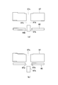
次に、上記の従来の音響センサ1において生じ得る不都合について説明する。図3は、音響センサ1に過大な圧力が作用した場合について記載した模式図である。図3に示すように、過大な圧力が音響センサ1に作用した場合には、大圧力がバックプレート7に設けられた音孔7aから振動電極膜5の振動部11に作用し、振動部11に大きな歪が生じ、振動電極膜5が破損してしまう場合があった。このような不都合は、例えば音響センサ1に過大な空気圧が作用した場合の他、音響センサ1が落下した場合等にも生じ得る。
Next, inconveniences that may occur in the conventional acoustic sensor 1 will be described. FIG. 3 is a schematic diagram illustrating a case where an excessive pressure is applied to the acoustic sensor 1. As shown in FIG. 3, when an excessive pressure acts on the acoustic sensor 1, the large pressure acts on the vibrating portion 11 of the vibrating electrode film 5 from the sound hole 7 a provided in the back plate 7, and the vibrating portion 11. In such a case, a large distortion may occur, and the vibrating electrode film 5 may be damaged. Such an inconvenience may occur when, for example, excessive air pressure acts on the acoustic sensor 1 or when the acoustic sensor 1 falls.
これに対し、図4に示すような対策が考えられる。すなわち、図4(a)に示すように、振動電極膜5に対して、作用した圧力を解放するための孔5aを設けておくことで、図4(b)に示すように、音響センサ1のバックプレート7の音孔7aから過大な圧力が作用した場合には、孔5aから圧力を解放させることで、振動電極膜5の破損を防止することが可能である。しかしながら、振動電極膜5に上記のような常時開放している孔5aを設けると、圧力に対する耐性は向上するものの、特に低音域での感度低下、すなわちロールオフが発生し易くなり、音響センサ1の周波数特性が悪化するという不都合があった。
In response to this, a countermeasure as shown in FIG. 4 can be considered. That is, as shown in FIG. 4A, by providing the vibrating electrode film 5 with a hole 5a for releasing the applied pressure, the acoustic sensor 1 as shown in FIG. When excessive pressure is applied from the sound hole 7a of the back plate 7, it is possible to prevent the vibration electrode film 5 from being damaged by releasing the pressure from the hole 5a. However, when the vibration electrode film 5 is provided with the hole 5a that is always open as described above, although the resistance to pressure is improved, sensitivity is lowered particularly in the low frequency range, that is, roll-off is likely to occur, and the acoustic sensor 1 There is a disadvantage that the frequency characteristics of the above deteriorate.
また、振動電極膜と、該振動電極膜をスリットで区切って分離した一画であるプラグ部とを有しており、プラグ部を、バックプレートに対して支持構造によって振動電極膜の他の部分と同じ高さに支持されるようにする対策が考えられる。この対策においては、振動電極膜が膜の両側の圧力差に応答して変位することで、プラグ部との間の流路が拡大することによって、過大な圧力を解放する(例えば、特許文献2を参照)。
In addition, the vibration electrode film has a plug portion which is a single part separated by dividing the vibration electrode film by a slit, and the plug portion is supported by another structure on the back plate by another structure. Measures to ensure that it is supported at the same height. In this countermeasure, the vibrating electrode film is displaced in response to the pressure difference between the two sides of the film, so that the flow path between the plug portion and the plug portion is expanded to release excessive pressure (for example, Patent Document 2). See).
しかし、この対策には以下のような不都合があった。まず、プラグ部は、非常に薄い振動電極膜の一画を用いて構成されているので、破損し易い。また、蓋状のプラグ部がバックプレートに対して、棒状の別部材からなる支持構造を用いて支持されているので、製造工程が複雑化するばかりでなく、支持構造からプラグ部が破損脱落する虞がある。
However, this measure has the following inconveniences. First, since the plug portion is configured using a very thin portion of the vibrating electrode film, it is easily damaged. In addition, since the lid-like plug portion is supported with respect to the back plate by using a support structure made of a separate bar-like member, not only the manufacturing process is complicated, but the plug portion is damaged and dropped from the support structure. There is a fear.
また、この対策では、振動電極膜が膜の両側の圧力差に応答して変位することで、該振動電極膜と、該振動電極膜をスリットで区切って分離した一画であるプラグ部との間の流動経路を拡大させ、過大な圧力を解放している。すなわち、振動電極膜及び、該振動電極膜をスリットで区切って分離した一画であるプラグ部という、薄膜どうしの間の隙間を流路として利用しているので、比較的大きな圧力を受けて振動電極膜の振幅が大きくなると、使用圧力範囲内であっても、プラグ部と振動電極膜の位置が膜厚以上にずれ、流路がやや拡大した状態となり、音響センサ1の周波数特性が不安定になる虞がある。
Further, in this measure, the vibrating electrode film is displaced in response to a pressure difference on both sides of the film, so that the vibrating electrode film and a plug portion which is a single part separated by dividing the vibrating electrode film by a slit. The flow path between them is expanded and the excessive pressure is released. In other words, the vibration electrode film and the plug part, which is a part of the vibration electrode film separated by a slit, are used as a flow path between the thin films. When the amplitude of the electrode film is increased, the position of the plug portion and the vibrating electrode film is shifted beyond the film thickness even in the operating pressure range, and the flow path is slightly expanded, and the frequency characteristics of the acoustic sensor 1 are unstable. There is a risk of becoming.
上記のような不具合に対し、印加された圧力を解放する孔を振動電極膜に備えることとし、そして、振動電極膜の変形前の状態においては、バックプレートの一部であり凸状に形成された柱構造が孔を貫通して少なくともその一部を閉鎖するとともに、振動電極膜が圧力を受けて変形した状態においては、振動電極膜とバックプレートとの相対移動によって、バックプレートの柱構造による孔の貫通が解除されて孔の全体が露出することにより、振動電極膜に印加された圧力が解放されるようにする対策が考えられた。
For the above problems, the vibration electrode film is provided with a hole for releasing the applied pressure, and in the state before the deformation of the vibration electrode film, it is a part of the back plate and is formed in a convex shape. In the state where the pillar structure penetrates the hole and closes at least a part thereof and the vibrating electrode film is deformed by receiving pressure, the relative movement between the vibrating electrode film and the back plate causes the back plate to have a pillar structure. A measure was taken to release the pressure applied to the vibrating electrode film by releasing the penetration of the hole and exposing the entire hole.
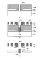
図5には、上記のような対策を講じた場合の、音響センサの振動電極膜15及びバックプレート17付近の概略図を示す。図5(a)は、振動電極膜15の平面図、図5(b)は、振動電極膜15及びバックプレート17、基板13の断面B-B´についての断面図である。図5(a)に示すように、この対策においては、振動電極膜15の振動部21の四隅には、圧力解放孔15bが設けられている。そして、図5(b)に示すように、振動電極膜15に過大な圧力が作用する前の状態では、バックプレート17に一体的に凸状に設けられた柱構造である凸部17bが圧力解放孔15bを貫通することで、圧力解放孔15bを閉鎖するように構成されている。なお、この凸部17bは、バックプレート17が半導体製造工程で形成される際に、同時にバックプレート17の一部として形成されたものである。
FIG. 5 shows a schematic view of the vicinity of the vibration electrode film 15 and the back plate 17 of the acoustic sensor when the above-described measures are taken. 5A is a plan view of the vibrating electrode film 15, and FIG. 5B is a cross-sectional view of the vibrating electrode film 15, the back plate 17, and the substrate 13 taken along the section BB ′. As shown in FIG. 5A, in this measure, pressure release holes 15 b are provided at the four corners of the vibrating portion 21 of the vibrating electrode film 15. As shown in FIG. 5B, in a state before excessive pressure is applied to the vibrating electrode film 15, the convex portion 17b, which is a columnar structure integrally provided on the back plate 17, is pressurized. By passing through the release hole 15b, the pressure release hole 15b is closed. The convex portion 17 b is formed as a part of the back plate 17 at the same time when the back plate 17 is formed in the semiconductor manufacturing process.
次に、図6を用いて、上記の圧力解放孔15b及び凸部17bの作用について説明する。図6(a)は、振動電極膜15に過大な圧力が作用する前の状態を示す。図6(b)は、振動電極膜15に過大な圧力が作用することにより、振動電極膜15が大きく変形した状態を示す。図6(a)に示すように、振動電極膜15の変形前の状態においては、バックプレート17の凸部17bが振動電極膜15に設けられた圧力解放孔15bを貫通して閉鎖した状態となっており、この状態においては、振動電極膜15にバックプレート17側から圧力が作用した場合に、圧力解放孔15bを通過する空気の量は少なく、圧力は充分に解放されない。
Next, the operation of the pressure release hole 15b and the convex portion 17b will be described with reference to FIG. FIG. 6A shows a state before an excessive pressure is applied to the vibrating electrode film 15. FIG. 6B shows a state in which the vibrating electrode film 15 is greatly deformed by an excessive pressure acting on the vibrating electrode film 15. As shown in FIG. 6A, in a state before the vibration electrode film 15 is deformed, the convex portion 17b of the back plate 17 passes through the pressure release hole 15b provided in the vibration electrode film 15 and is closed. In this state, when pressure is applied to the vibrating electrode film 15 from the back plate 17 side, the amount of air passing through the pressure release hole 15b is small and the pressure is not sufficiently released.
しかしながら、振動電極膜15に過大な圧力が作用した場合には、当該圧力によって振動電極膜15が大きく変形し図6(b)に示すようにバックプレート17から離れる方向に変形する。そうすると、凸部17bが圧力解放孔15bから抜け(貫通が解除され)、圧力解放孔15bの閉鎖が解消される。そのことにより、振動電極膜15に圧力を作用させている空気が圧力解放孔15bから図中下側に抜けることで、振動電極膜15に作用する圧力が瞬時に解放される。これにより、凸部17bが圧力解放孔15bから抜けた後の振動電極膜15の更なる変形が抑制され、振動電極膜15の破損を回避することが可能となる。
However, when an excessive pressure is applied to the vibrating electrode film 15, the vibrating electrode film 15 is greatly deformed by the pressure and is deformed away from the back plate 17 as shown in FIG. 6B. If it does so, the convex part 17b will come out from the pressure release hole 15b (penetration will be cancelled | released), and the closure of the pressure release hole 15b will be eliminated. As a result, the air acting on the vibration electrode film 15 is released downward from the pressure release hole 15b in the drawing, so that the pressure acting on the vibration electrode film 15 is instantaneously released. As a result, further deformation of the vibrating electrode film 15 after the convex portion 17b is removed from the pressure release hole 15b is suppressed, and breakage of the vibrating electrode film 15 can be avoided.
次に、図7には、上述した対策において、凸部27bの径が、無段階で直線的に先端へいくほど細くなる例について図示する。このような場合には、過大な圧力が振動電極膜25に作用し、振動電極膜25が大きく変形した状態においては、凸部27bの先端側の小径の部分が圧力解放孔25bを貫通している状態となり、圧力を解放する空気の流路面積が増大するので、振動電極膜25の過剰な変形を防止できる。
Next, FIG. 7 illustrates an example in which the diameter of the convex portion 27b becomes smaller in a stepless manner linearly toward the tip in the above-described countermeasure. In such a case, when the excessive pressure acts on the vibrating electrode film 25 and the vibrating electrode film 25 is greatly deformed, the small diameter portion on the tip side of the convex portion 27b penetrates the pressure release hole 25b. As a result, the flow area of the air that releases the pressure increases, so that excessive deformation of the vibrating electrode film 25 can be prevented.
ところで、上記のような従来の対策においては、圧力が上(すなわち、バックプレート側)から作用することにより、振動電極膜が上側から下側に移動した場合には、良好に圧力を解放することが可能であるが、圧力が下から作用することにより、振動電極膜が下側から上側に移動した場合には、圧力を解放する空気の流路面積を増大させることができず、振動電極膜の上側への過剰な変形を防止することができなかった。
By the way, in the conventional measures as described above, when the vibrating electrode film moves from the upper side to the lower side due to the pressure acting from above (that is, the back plate side), the pressure is released well. However, when the vibrating electrode film moves from the lower side to the upper side due to the pressure acting from below, the flow area of the air for releasing the pressure cannot be increased, and the vibrating electrode film It was not possible to prevent excessive deformation of the upper side of the plate.
例えば、凸部27bの径が、無段階で直線的に先端へいくほど細くなる例においては、図8(a)に示すように、振動電極膜25が下側から上側に移動した場合には、圧力を解放する空気の流路面積が逆に減少してしまい、振動電極膜25の上側への過剰な変形を防止することができなかった。
For example, in an example in which the diameter of the convex portion 27b becomes thinner steplessly and linearly toward the tip, as shown in FIG. 8A, when the vibrating electrode film 25 moves from the lower side to the upper side, On the contrary, the flow area of the air for releasing the pressure is reduced, and the excessive deformation of the vibrating electrode film 25 to the upper side cannot be prevented.
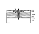
これに対し、本実施例においては、図8(b)に示すように、凸部37bのバックプレート37に平行方向の断面積が、無段階で直線的に根元、すなわちバックプレート37側にいくほど小さくなるようにした。これによれば、過大な圧力が下側から振動電極膜35に作用し、振動電極膜35が上側に大きく変形した状態においても、凸部37bの根元側の断面積が小さい部分が圧力解放孔35bを貫通している状態となり、圧力を解放する空気の流路面積が増大するので、振動電極膜35の過剰な変形を防止できる。
On the other hand, in the present embodiment, as shown in FIG. 8B, the cross-sectional area of the convex portion 37b in the direction parallel to the back plate 37 is steplessly linearly toward the root, that is, the back plate 37 side. I tried to make it smaller. According to this, even when excessive pressure acts on the vibrating electrode film 35 from the lower side and the vibrating electrode film 35 is greatly deformed upward, the portion having a small cross-sectional area on the base side of the convex portion 37b is the pressure release hole. Since the air passage area through which the pressure is released is increased, the excessive deformation of the vibrating electrode film 35 can be prevented.
一方、本実施例において、過大な圧力が上側(すなわちバックプレート37側)から振動電極膜35に作用し、振動電極膜35が下側に大きく変形した状態においては、凸部37bの先端側の断面積の大きい部分が圧力解放孔35bを貫通している状態となり、圧力を解放する空気の流路面積が一旦減少するが、凸部37bが、振動電極膜35の圧力解放孔35bから抜けた時点で、圧力を解放する十分な大きさの空気の流路面積を得ることが可能である。結果として、本実施例によれば、過大な圧力が上下いずれの方向から振動電極膜35に作用したとしても、振動電極膜35の過剰な変形を防止できる。
On the other hand, in this embodiment, when excessive pressure is applied to the vibrating electrode film 35 from the upper side (that is, the back plate 37 side) and the vibrating electrode film 35 is greatly deformed to the lower side, A portion having a large cross-sectional area passes through the pressure release hole 35b, and the flow area of the air releasing the pressure is temporarily reduced. However, the convex portion 37b is removed from the pressure release hole 35b of the vibration electrode film 35. At that point, it is possible to obtain a sufficiently large air flow area to release the pressure. As a result, according to this embodiment, even if an excessive pressure is applied to the vibrating electrode film 35 from any direction, it is possible to prevent excessive deformation of the vibrating electrode film 35.
次に、本実施例における図9~図10を用いて、本実施例における凸部と、圧力解放孔の形成プロセスについて説明する。まず、図9(a)に示すように、シリコン(Si)基板43の表面に酸化シリコン(SiO2)の絶縁層44aが形成され、絶縁層44aの上に振動電極膜となるべきポリシリコン(Poly Si)膜45が形成される。次に、振動電極膜となるべきポリシリコン(Poly Si)の膜45がエッチングにより部分的に除去されて圧力解放孔45bとなる部分が形成される。
Next, the formation process of the convex portion and the pressure release hole in this embodiment will be described with reference to FIGS. 9 to 10 in this embodiment. First, as shown in FIG. 9A, an insulating layer 44a of silicon oxide (SiO2) is formed on the surface of a silicon (Si) substrate 43, and polysilicon (Poly) to be a vibrating electrode film is formed on the insulating layer 44a. A Si) film 45 is formed. Next, the polysilicon (Poly Si) film 45 to be the vibrating electrode film is partially removed by etching to form a portion that becomes the pressure release hole 45b.
次に、図9(b)に示すように、ポリシリコン(Poly Si)の膜45の上に凸部を形成するための窒化シリコン(SiN)膜46が形成される。そして、図9(c)に示すように、フォトレジストを使ったエッチングにより、凸部47bとなる部分のみを残して窒化シリコン(SiN)膜46を除去する。その際、エッチングの垂直方向の指向性を弱める手法によりテーパ形状を実現することができる。
Next, as shown in FIG. 9B, a silicon nitride (SiN) film 46 for forming convex portions is formed on the polysilicon (Poly Si) film 45. Then, as shown in FIG. 9C, the silicon nitride (SiN) film 46 is removed by etching using a photoresist, leaving only the portions that become the convex portions 47b. At that time, the taper shape can be realized by a technique of weakening the directivity in the vertical direction of etching.
次に、図10(a)に示すように、さらに酸化シリコン(SiO2)の犠牲層44bを製膜する。そして、CMP(Chemical Mechanical Polishing)法などの平坦化手法を適用することで、窒化シリコン(SiN)からなる凸部47bが酸化シリコン(SiO2)の中に埋もれる形となる。次に、図10(b)に示すように、バックプレート47となる窒化シリコン(SiN)膜を製膜することで、逆テーパ型の凸部47bを有するバックプレート47が形成される。
Next, as shown in FIG. 10A, a sacrificial layer 44b of silicon oxide (SiO2) is further formed. Then, by applying a planarization method such as CMP (Chemical-Mechanical-Polishing) method, the convex portion 47b made of silicon nitride (SiN) is buried in the silicon oxide (SiO2). Next, as shown in FIG. 10B, a silicon nitride (SiN) film to be the back plate 47 is formed, thereby forming the back plate 47 having the reverse taper type convex portions 47b.
次に、一般的な音響センサの製造プロセスと同様に、Si基板43をエッチングにより除去し、フッ酸(HF)により酸化シリコン(SiO2)の絶縁層44a及び犠牲層44bをエッチングして除去することで、図10(c)に示すような凸部47bを有するバックプレート47と、圧力解放孔45bを有する振動電極膜45を形成することが可能である。
Next, similarly to a general acoustic sensor manufacturing process, the Si substrate 43 is removed by etching, and the insulating layer 44a and the sacrificial layer 44b of silicon oxide (SiO2) are removed by etching with hydrofluoric acid (HF). Thus, it is possible to form the back plate 47 having the convex portions 47b and the vibrating electrode film 45 having the pressure release holes 45b as shown in FIG.
次に、図11~図12を用いて、本実施例における凸部と、圧力解放孔の形成プロセスの第2の例について説明する。まず、図11(a)に示すように、シリコン(Si)基板52の表面にPSG(リンを含んだ酸化シリコン(SiO2)の膜53)が形成され、膜53の上に不純物を含まない酸化シリコン(SiO2)の膜であるNSG54a形成される。また、NSG54a上には、振動電極膜となるべきポリシリコン(Poly Si)の膜55が形成されさらにエッチングにより部分的に除去されて圧力解放孔55bとなる部分が形成される。さらに、その上にNSG54b形成される。
Next, a second example of the formation process of the convex portion and the pressure release hole in this embodiment will be described with reference to FIGS. First, as shown in FIG. 11A, PSG (silicon oxide (SiO 2) film 53 containing phosphorus) is formed on the surface of a silicon (Si) substrate 52, and an oxide containing no impurities is formed on the film 53. An NSG 54a which is a silicon (SiO2) film is formed. Further, on the NSG 54a, a polysilicon (Poly Si) film 55 to be a vibrating electrode film is formed, and further, a portion to be a pressure release hole 55b is formed by being partially removed by etching. Further, NSG 54b is formed thereon.
次に、図11(b)に示すように、NSG54a上に、凸部を形成する部分に開口が設けられたフォトレジストを形成し、HF水溶液でNSG54a、54bの凸部に相当する部分をエッチングにより除去する。HF水溶液によるエッチングは等方的に進行し、図11(c)に示すように、PSG53をも除去して、シリコン(Si)基板52の表面に達する。
Next, as shown in FIG. 11B, on the NSG 54a, a photoresist having an opening provided in a portion where the convex portion is formed is formed, and a portion corresponding to the convex portion of the NSG 54a, 54b is etched with an HF aqueous solution. Remove with. Etching with the HF aqueous solution proceeds isotropically, and PSG 53 is also removed and reaches the surface of the silicon (Si) substrate 52 as shown in FIG.
次に、図12(a)に示すように、PSG膜53においては、NSG膜54a、54bと比較してエッチングレートが数倍程度速いため、水平方向にエッチングが速く進行する。また、NSG膜54a、54bにおいては、下層よりエッチングが進行するため、NSG膜54a、54bには図12(b)に示すような、図12(a)とは逆のテーパ形状の空間が形成される。
Next, as shown in FIG. 12A, in the PSG film 53, the etching rate is about several times faster than that of the NSG films 54a and 54b. In addition, since the NSG films 54a and 54b are etched from the lower layer, a space having a tapered shape opposite to that shown in FIG. 12A is formed in the NSG films 54a and 54b as shown in FIG. Is done.
次に、図12(c)に示すように、フォトレジストを除去した後に、バックプレート57及び凸部57bとなる窒化シリコン(SiN)膜を製膜することで、逆テーパ型の凸部57bを有するバックプレート57が形成される。
Next, as shown in FIG. 12C, after removing the photoresist, a silicon nitride (SiN) film to be the back plate 57 and the convex portion 57b is formed, so that the inverted tapered convex portion 57b is formed. A back plate 57 is formed.
なお、本実施例においては、PSG膜53及び、NSG膜54a、54bを用いてプロセスを実行したが、これは一例に過ぎない。エッチングレートの異なる組み合わせであれば、他の材質の組み合わせを用いても構わない。例えば、アニールを行うことでエッチングレートを高めた酸化シリコン(SiO2)と、アニールを行っていない酸化シリコン(SiO2)の組み合わせや、エッチングレートの高いTEOS膜とエッチングレートの低い熱酸化膜の組み合わせを用いても良い。
In this embodiment, the process is executed using the PSG film 53 and the NSG films 54a and 54b, but this is only an example. Other combinations of materials may be used as long as the etching rates are different. For example, a combination of silicon oxide (SiO 2) whose etching rate has been increased by annealing and silicon oxide (SiO 2) which has not been annealed, or a combination of a TEOS film having a high etching rate and a thermal oxide film having a low etching rate. It may be used.
次に、図13を用いて、本実施例における凸部と、圧力解放孔の形成プロセスの第3の例について説明する。まず、図13(a)に示すように、シリコン(Si)基板63の表面にPSG膜(リンを含んだ酸化シリコン(SiO2)の膜64)が形成され、膜64の上には、振動電極膜となるべきポリシリコン(Poly Si)の膜65が形成されさらにエッチングにより部分的に除去されて圧力解放孔65bとなる部分が形成される。また、膜64の上には不純物を含まない酸化シリコン(SiO2)の膜であるNSG膜66が形成される。また、NSG膜66上には、さらに、PSG(リンを含んだ酸化シリコン(SiO2)膜68が形成され、その上には、凸部を形成する部分に開口が設けられたフォトレジストが69形成される。
Next, a third example of the formation process of the convex portion and the pressure release hole in this embodiment will be described with reference to FIG. First, as shown in FIG. 13A, a PSG film (a film 64 of silicon oxide (SiO 2) containing phosphorus) is formed on the surface of a silicon (Si) substrate 63, and a vibrating electrode is formed on the film 64. A polysilicon (Poly Si) film 65 to be a film is formed and further removed by etching to form a portion to be a pressure release hole 65b. Further, an NSG film 66 which is a silicon oxide (SiO 2) film not containing impurities is formed on the film 64. Further, a PSG (phosphorus-containing silicon oxide (SiO 2) film 68 is further formed on the NSG film 66, and a photoresist 69 having an opening in a portion where a convex portion is formed is formed thereon. Is done.
次に、図13(b)に示すように、フッ酸(HF)水溶液で、PSG膜(リンを含んだ酸化シリコン(SiO2)の膜64、68)と、NSG膜66の凸部に相当する部分をエッチングにより除去する。この場合、各層におけるエッチングレートの相違により、斜面の形状が様々に調整可能である。そして、HF水溶液によるエッチングは、PSG膜64をも除去して、シリコン(Si)基板63の表面に達する。
Next, as shown in FIG. 13B, a hydrofluoric acid (HF) aqueous solution corresponds to a PSG film (silicon oxide (SiO 2) films 64 and 68 containing phosphorus) and a convex portion of the NSG film 66. The part is removed by etching. In this case, the shape of the slope can be variously adjusted depending on the etching rate in each layer. Then, the etching with the HF aqueous solution also removes the PSG film 64 and reaches the surface of the silicon (Si) substrate 63.
次に、図13(c)に示すように、フォトレジストを除去した後に、バックプレート67及び凸部67bとなる窒化シリコン(SiN)膜を製膜することで、逆テーパ型の凸部67bを有するバックプレート67が形成される。
Next, as shown in FIG. 13C, after removing the photoresist, a silicon nitride (SiN) film to be the back plate 67 and the convex portion 67b is formed, so that the inverted tapered convex portion 67b is formed. A back plate 67 is formed.
なお、本実施例においては、最も上側の層をPSG膜68としたが、このPSG膜68は必ずしも必要ではない。PSG膜68を省略したとしても、一般的にフォトレジスト69の密着面はエッチングレートが局所的に早くなる傾向があるので、このエッチングレートの傾向を利用して、同等の形状を生成することが可能である。
In the present embodiment, the uppermost layer is the PSG film 68, but this PSG film 68 is not necessarily required. Even if the PSG film 68 is omitted, the contact surface of the photoresist 69 generally tends to have a locally high etching rate. Therefore, this etching rate tendency can be used to generate an equivalent shape. Is possible.
なお、本実施例の凸部67bにおいて、少なくとも平均より水平方向の断面積が小さくなるバックプレート67側の領域は本発明の所定の領域に相当する。また、凸部67bにおいて少なくとも平均より水平方向の断面積が小さくなる部分は断面積減少部に相当する。
In addition, in the convex part 67b of a present Example, the area | region by the side of the backplate 67 in which the cross-sectional area of a horizontal direction becomes smaller than an average corresponds to the predetermined area | region of this invention. Further, at least a portion of the convex portion 67b whose horizontal sectional area is smaller than the average corresponds to a reduced sectional area.
<実施例2>
次に、本発明の実施例2について説明する。本実施例においては、バックプレートに一体に設けられた略円柱状の凸部に対して、水平方向については凸部の側面を含む形で、垂直方向については凸部の途中までの領域に音孔を形成することで、凸部の根元側においては圧力解放のための流路面積を増加させた例について説明する。 <Example 2>
Next, a second embodiment of the present invention will be described. In the present embodiment, with respect to the substantially cylindrical convex portion integrally provided on the back plate, the horizontal direction includes the side surface of the convex portion, and in the vertical direction, sound is generated in the region up to the middle of the convex portion. An example in which the passage area for pressure release is increased on the base side of the convex portion by forming the hole will be described.
図14には、本実施例におけるバックプレート77に形成された凸部77bと、振動電極膜75に設けられた圧力解放孔75bの断面図を示す。本実施例における凸部77bは、概略円柱状の形状を形成し、バックプレート77における音孔をエッチングで形成する際に、水平方向については円柱状の凸部77bの側面を含む形で、垂直方向については円柱状の凸部77bの途中まで、凸部77bの先端部を残す形で空間77cを形成することで完成する。
FIG. 14 shows a cross-sectional view of the convex portion 77b formed on the back plate 77 and the pressure release hole 75b provided in the vibration electrode film 75 in this embodiment. The convex portion 77b in the present embodiment has a substantially cylindrical shape, and when the sound holes in the back plate 77 are formed by etching, the horizontal direction includes the side surface of the cylindrical convex portion 77b, and is vertical. About the direction, it completes by forming the space 77c in the form which leaves the front-end | tip part of the convex part 77b to the middle of the cylindrical convex part 77b.
これによれば、凸部77bの側面における、バックプレート77側の領域には、空間77cが凸部77bの側面と交差することにより形成される開口部77dが開口している形状となる。そうすると、図14に示す状態より、振動電極膜75にバックプレート77とは反対側(図中下側)から過大な圧力が作用した場合に、振動電極膜75がバックプレート77側(図中上側)に変形する。そして、振動電極膜75が開口部77dの下端よりさらにバックプレート77側まで変形した際には、振動電極膜75に圧力を作用させている空気が開口部77dから空間77cを通じてバックプレート77の上側に逃げることで、振動電極膜75にバックプレート77と逆側から作用している圧力は解放される。
According to this, in the region on the side of the back plate 77 on the side surface of the convex portion 77b, an opening 77d formed by the space 77c intersecting the side surface of the convex portion 77b is opened. Then, in the state shown in FIG. 14, when excessive pressure is applied to the vibrating electrode film 75 from the side opposite to the back plate 77 (lower side in the figure), the vibrating electrode film 75 is moved to the back plate 77 side (upper side in the figure). ). When the vibrating electrode film 75 is further deformed from the lower end of the opening 77d to the back plate 77 side, the air that exerts pressure on the vibrating electrode film 75 passes from the opening 77d to the upper side of the back plate 77 through the space 77c. The pressure acting on the vibrating electrode film 75 from the side opposite to the back plate 77 is released.
これによれば、凸部77bが形成されたバックプレート77に音孔を形成するプロセスにおいて、同時に、平面視において凸部77bの側面を含むように空間77cを形成することで、凸部77bのバックプレート77側の領域において容易に凸部77bの断面積を減少させることが可能である。ここで、凸部77bの高さ方向の領域であって、空間77cが形成された領域は、本発明の所定の領域に相当する。また、凸部77bにおいて空間77cが形成された部分は断面積減少部に相当する。
According to this, in the process of forming the sound hole in the back plate 77 on which the convex portion 77b is formed, at the same time, by forming the space 77c so as to include the side surface of the convex portion 77b in plan view, It is possible to easily reduce the cross-sectional area of the convex portion 77b in the region on the back plate 77 side. Here, the region in the height direction of the convex portion 77b and in which the space 77c is formed corresponds to a predetermined region of the present invention. Further, the portion of the convex portion 77b where the space 77c is formed corresponds to a cross-sectional area decreasing portion.
<実施例3>
次に、本発明の実施例3として、バックプレートから離れ先端側にいくに従って径が小さくなるようなテーパ状の形状を有する凸部に対して、側面の途中からバックプレート側において開口する開口部と、この開口部とバックプレートの上側とを貫通する空間とを形成した例について説明する。 <Example 3>
Next, as Example 3 of the present invention, an opening that opens on the back plate side from the middle of the side surface with respect to a convex portion having a tapered shape whose diameter decreases from the back plate toward the tip side. An example in which a space penetrating the opening and the upper side of the back plate is formed will be described.
図15は、従来の、バックプレートから離れ先端側にいくに従って径が小さくなるようなテーパ状の形状を有する凸部を有する場合と、当該凸部に対して、側面の途中からバックプレート側において開口する開口部と、この開口部とバックプレートの上側とを貫通する空間とを形成した場合の作用を示す図である。
FIG. 15 shows a case where a conventional convex portion having a tapered shape whose diameter decreases from the back plate toward the distal end side and the convex portion on the back plate side from the middle of the side surface. It is a figure which shows an effect | action at the time of forming the opening part which opens and the space which penetrates this opening part and the upper side of a backplate.
図15(a)は、通常のテーパ状の凸部を有する場合、図15(b)は、テーパ状の凸部に上記の開口部と、開口部とバックプレートの上側とを貫通する空間とを形成した場合について示す。図15(a)に示すように、凸部87bが単なるテーパ形状を有する場合には、振動電極膜85にバックプレート87と反対側から過大な圧力が作用した場合には、振動電極膜85がバックプレート87側に変形する。そして、その際、振動電極膜85がバックプレート87側に変形すればする程、凸部87bと圧力解放孔85bとの間の隙間の面積が減少するため、さらに圧力を解放しづらくなる。
FIG. 15A shows a case where a normal taper-shaped convex portion is provided, and FIG. 15B shows a case where the taper-shaped convex portion has the above-described opening and a space penetrating the opening and the upper side of the back plate. It shows about the case where is formed. As shown in FIG. 15A, when the convex portion 87b has a simple taper shape, if excessive pressure is applied to the vibration electrode film 85 from the side opposite to the back plate 87, the vibration electrode film 85 Deforms to the back plate 87 side. At that time, the more the vibrating electrode film 85 is deformed to the back plate 87 side, the smaller the area of the gap between the convex portion 87b and the pressure release hole 85b becomes, and it becomes more difficult to release the pressure.
それに対して、図15(b)に示すように、テーパ状の凸部のバックプレート87側の領域に開口部87dと、開口部87dとバックプレート87の上側とを貫通する空間87cとを形成した場合については異なる挙動が示される。すなわち、振動電極膜85にバックプレート87と反対側から過大な圧力が作用した場合には、振動電極膜85がバックプレート87側に変形するが、振動電極膜85が開口部87dの存在する領域に達した際には、開口部87d、空間87cを介して、振動電極膜85に作用している圧力に係る空気をバックプレート87の上側に逃がすことができる。
On the other hand, as shown in FIG. 15B, an opening 87d and a space 87c penetrating the opening 87d and the upper side of the back plate 87 are formed in the region on the back plate 87 side of the tapered convex portion. Different behavior is shown for the case. That is, when an excessive pressure is applied to the vibration electrode film 85 from the side opposite to the back plate 87, the vibration electrode film 85 is deformed to the back plate 87 side, but the vibration electrode film 85 is an area where the opening 87d exists. Can reach the upper side of the back plate 87 through the opening 87d and the space 87c.
よって、この時点で振動電極膜85に作用している圧力を解放することができ、それ以上の振動電極膜85の変形を防止することが可能となる。また、本実施例においては、バックプレート87と反対側からの圧力を振動電極膜85に作用させる空気に異物等が混入していた場合には、上記の開口部87d及び空間87cを介して異物を逃がすことができるため、凸部87bと、圧力解放孔85bの間や、その近傍に異物が挟まったり堆積したりするリスクを低減することが可能である。
Therefore, the pressure acting on the vibrating electrode film 85 at this point can be released, and further deformation of the vibrating electrode film 85 can be prevented. In this embodiment, when foreign matter or the like is mixed in the air that causes the pressure from the side opposite to the back plate 87 to act on the vibrating electrode film 85, the foreign matter is passed through the opening 87d and the space 87c. Therefore, it is possible to reduce the risk of foreign matter being caught or deposited between the convex portion 87b and the pressure release hole 85b or in the vicinity thereof.
なお、本実施例の構成を採用した場合には、バックプレート87に、図16に示すようなストッパ87eを設けてもよい。本来、ストッパ87eは、バックプレート87と、振動電極膜85とが固着したり、両者の接触時に電気的にショートしたりすることを防止するためのものであるが、本実施例においては、このストッパ87eの高さをh1、開口部87dのバックプレート87からの深さをd1、振動電極膜85の厚みをt1とした場合に、
d1>h1+t1・・・・・(1)
が成立するようにした。 When the configuration of this embodiment is adopted, astopper 87e as shown in FIG. 16 may be provided on the back plate 87. Originally, the stopper 87e is intended to prevent the back plate 87 and the vibrating electrode film 85 from being fixed or electrically short-circuited when they are in contact with each other. When the height of the stopper 87e is h1, the depth of the opening 87d from the back plate 87 is d1, and the thickness of the vibration electrode film 85 is t1,
d1> h1 + t1 (1)
Was made to hold.
d1>h1+t1・・・・・(1)
が成立するようにした。 When the configuration of this embodiment is adopted, a
d1> h1 + t1 (1)
Was made to hold.
これによれば、過大な圧力がバックプレート87の反対側から振動電極膜85に作用した場合には、振動電極膜85がバックプレート87側に変位するが、その際、振動電極膜85がバックプレート87のストッパ87eに当接するまで変位し、当接したところで安定した姿勢が維持される。そして、その状態において確実に、開口部87dの一部が、振動電極膜85のバックプレート87の反対側に開口される。よって、過大な圧力がバックプレート87の反対側から振動電極膜85に作用した場合に、より確実に、開口部87d及び空間87cを介して、空気をバックプレート87の上側に逃がし、振動電極膜85に作用している圧力を解放することが可能となる。なお、図15においては、開口部87dの下端部の高さは、凸部87bの内壁の底部と同一面となっていたが、開口部87dの下端部の高さは、必ずしも凸部87bの内壁の底部と同一面でなくてもよい。図16に示すように、別面としても構わない。
According to this, when an excessive pressure is applied to the vibration electrode film 85 from the opposite side of the back plate 87, the vibration electrode film 85 is displaced to the back plate 87 side. The plate 87 is displaced until it abuts against the stopper 87e of the plate 87, and a stable posture is maintained at the abutment. In this state, a part of the opening 87d is surely opened on the opposite side of the back plate 87 of the vibrating electrode film 85. Therefore, when excessive pressure is applied to the vibrating electrode film 85 from the opposite side of the back plate 87, air is more reliably released to the upper side of the back plate 87 through the opening 87d and the space 87c. The pressure acting on 85 can be released. In FIG. 15, the height of the lower end of the opening 87d is flush with the bottom of the inner wall of the protrusion 87b, but the height of the lower end of the opening 87d is not necessarily the height of the protrusion 87b. It may not be flush with the bottom of the inner wall. As shown in FIG. 16, it may be a different surface.
また、本実施例においてはバックプレート87にストッパ87eが設けられているが、ストッパとして機能する突起は振動電極膜85に設けられていてもよい。振動電極膜85の一部を突出させるもしくは振動電極膜85の上部に別途構造体を設けるなどしておくことで、上記したストッパ87eを設けた場合と同様、バックプレート87との固着を抑制できる等の効果が期待できる。そして、ストッパの高さh1、開口部のバックプレートからの深さd1、振動電極膜の厚みt1の間に(1)式が成立するようにすることで、本実施例の効果を得ることが可能である。
In this embodiment, the back plate 87 is provided with the stopper 87e, but the protrusion functioning as a stopper may be provided on the vibration electrode film 85. By causing a part of the vibrating electrode film 85 to protrude or providing a separate structure on the upper part of the vibrating electrode film 85, the sticking to the back plate 87 can be suppressed as in the case where the stopper 87e is provided. Such effects can be expected. The effect of this embodiment can be obtained by satisfying the expression (1) among the height h1 of the stopper, the depth d1 of the opening from the back plate, and the thickness t1 of the vibration electrode film. Is possible.
<実施例4>
次に、本発明の実施例4について説明する。本実施例においては、振動電極膜に設けられた圧力解放孔をスリット状とし、バックプレートに設けられた凸部は円柱状またはテーパ状ではなく、圧力解放孔に侵入可能な平板状の形状を有する例について説明する。 <Example 4>
Next, a fourth embodiment of the present invention will be described. In this embodiment, the pressure release hole provided in the vibrating electrode film is formed in a slit shape, and the convex portion provided in the back plate is not a columnar shape or a taper shape, but has a flat plate shape that can enter the pressure release hole. The example which has is demonstrated.
図17には、本実施例におけるバックプレート97及び凸部97b、振動電極膜95及び圧力解放孔95bの断面斜視図を示す。本実施例においては、上述のとおり、圧力解放孔95bは、平面視において円形ではなくスリット状である。また、凸部97bは、スリット状の圧力解放孔95bに侵入可能な平板状の形状を有する。図17においては、振動電極膜95及びバックプレート97を、スリット状の圧力解放孔95bと、平板状の凸部97bの中央部で切断した図を示している。スリット状の圧力解放孔95bと、平板状の凸部97bを採用した場合には、それらの幅が狭いことにより、半導体作製プロセスによりバックプレート97を平坦にし易くなり応力集中を軽減することができる。例えば、スリットの幅を、振動電極膜95とバックプレート97との間の距離の2倍以内とすることで、バックプレート97を平坦にし易くすることが可能である。
FIG. 17 shows a cross-sectional perspective view of the back plate 97 and the convex portion 97b, the vibrating electrode film 95, and the pressure release hole 95b in the present embodiment. In the present embodiment, as described above, the pressure release hole 95b has a slit shape instead of a circle in plan view. The convex portion 97b has a flat plate shape that can enter the slit-shaped pressure release hole 95b. FIG. 17 shows a view in which the vibrating electrode film 95 and the back plate 97 are cut at the center of the slit-shaped pressure release hole 95b and the flat plate-shaped convex portion 97b. When the slit-like pressure release hole 95b and the flat plate-like convex portion 97b are employed, the back plate 97 can be easily flattened by the semiconductor manufacturing process and the stress concentration can be reduced due to the narrow width thereof. . For example, the back plate 97 can be easily flattened by setting the width of the slit within twice the distance between the vibrating electrode film 95 and the back plate 97.
本実施例においては、バックプレート97に音孔97aを形成するプロセスにおいて、平板状の凸部97bに対しても、高さ方向の途中まで到達する空間97cを形成する。そうすると、平板状の凸部97bの左右両側において開口部97dが開口する形となる。なお、本実施例において、音孔97a及び空間97cの平面視による形状は円形が望ましい。これにより、バックプレート97の各部、特に平板状の凸部97bの近傍における応力集中を回避することが可能である。
In the present embodiment, in the process of forming the sound hole 97a in the back plate 97, a space 97c that reaches partway in the height direction is also formed with respect to the flat projection 97b. If it does so, it will become the shape which the opening part 97d opens in the right-and-left both sides of the flat convex part 97b. In the present embodiment, the shape of the sound hole 97a and the space 97c in plan view is preferably circular. Thereby, it is possible to avoid stress concentration in each part of the back plate 97, particularly in the vicinity of the flat plate-like convex part 97b.
図18は、本実施例におけるバックプレート97及び振動電極膜95の作用について説明するための図である。図18は、図17におけるバックプレート97及び振動電極膜95を断面の法線方向から見た断面図であり、図18(a)は振動電極膜95の変形前の状態を、図18(b)は、バックプレート97の反対側から振動電極膜95に過大な圧力が作用し振動電極膜95がバックプレート97側に変形した状態を示す。
FIG. 18 is a view for explaining the operation of the back plate 97 and the vibrating electrode film 95 in the present embodiment. 18 is a cross-sectional view of the back plate 97 and the vibrating electrode film 95 in FIG. 17 as viewed from the normal direction of the cross section. FIG. 18A shows a state before the vibrating electrode film 95 is deformed, and FIG. ) Shows a state where an excessive pressure is applied to the vibration electrode film 95 from the opposite side of the back plate 97 and the vibration electrode film 95 is deformed to the back plate 97 side.
本実施例によれば、バックプレート97の反対側から振動電極膜95に過大な圧力が作用し振動電極膜95がバックプレート97側に変形した場合に、平板状の凸部97bの左右両側に開口した開口部97dから、振動電極膜95に圧力を作用させる空気が空間97cを通過してバックプレート97の上側に逃げることが可能となる。これにより、振動電極膜95に作用する圧力を解放することができ、振動電極膜95の過剰な変形を防止することができる。
According to the present embodiment, when excessive pressure is applied to the vibration electrode film 95 from the opposite side of the back plate 97 and the vibration electrode film 95 is deformed to the back plate 97 side, From the opening 97d that is opened, air that applies pressure to the vibrating electrode film 95 can pass through the space 97c and escape to the upper side of the back plate 97. Thereby, the pressure acting on the vibrating electrode film 95 can be released, and excessive deformation of the vibrating electrode film 95 can be prevented.
一方、本実施例において、過大な圧力がバックプレート97側から振動電極膜95に作用し、振動電極膜95がバックプレート97とは反対側に大きく変形した状態においては、平板状の凸部97bが、振動電極膜95のスリット状の圧力解放孔95bから抜けた時点で、圧力解放孔95bの全体を空気が通過可能となる。従って、振動電極膜95に作用している圧力を解放するのに十分な大きさの空気の流路面積を得ることができる。結果として、本実施例によれば、過大な圧力が上下いずれの方向から振動電極膜95に作用したとしても、振動電極膜95の過剰な変形を防止することが可能である。
On the other hand, in the present embodiment, when the excessive pressure acts on the vibration electrode film 95 from the back plate 97 side and the vibration electrode film 95 is greatly deformed to the side opposite to the back plate 97, the plate-like convex portion 97b. However, air can pass through the entire pressure release hole 95b at the time when it comes out of the slit-like pressure release hole 95b of the vibrating electrode film 95. Therefore, a sufficiently large air flow area for releasing the pressure acting on the vibrating electrode film 95 can be obtained. As a result, according to the present embodiment, it is possible to prevent excessive deformation of the vibrating electrode film 95 even if an excessive pressure is applied to the vibrating electrode film 95 from either the upper or lower direction.
次に、図19を用いて、本実施例における凸部と、圧力解放孔の形成プロセスについて説明する。まず、図19(a)に示すように、シリコン(Si)基板103の表面に酸化シリコン(SiO2)の絶縁層104aが形成され、絶縁層104aの上に振動電極膜となるべきポリシリコン(Poly Si)膜105が形成され、エッチングにより当該ポリシリコン(Poly Si)膜105が部分的に除去されて圧力解放孔105bが形成される。そして、さらにポリシリコン(Poly Si)膜105の上に、酸化シリコン(SiO2)の犠牲層104bが形成された後、凸部となる部分の絶縁層104a及び犠牲層104bがエッチングにより除去される。
Next, the formation process of the convex part and the pressure release hole in this embodiment will be described with reference to FIG. First, as shown in FIG. 19A, an insulating layer 104a of silicon oxide (SiO2) is formed on the surface of a silicon (Si) substrate 103, and polysilicon (Poly) to be a vibrating electrode film is formed on the insulating layer 104a. Si) film 105 is formed, and the polysilicon (Poly Si) film 105 is partially removed by etching to form a pressure release hole 105b. Further, after a sacrificial layer 104b of silicon oxide (SiO 2) is formed on the polysilicon (Poly Si) film 105, the insulating layer 104a and the sacrificial layer 104b at the portions to be convex portions are removed by etching.
次に、図19(b)に示すように、固定電極膜となるポリシリコン(Poly Si)膜106が形成され、さらに、バックプレート及び凸部を形成するための窒化シリコン(SiN)膜107、107bが形成される。この際、凸部を形成するための窒化シリコン(SiN)膜107bが形成される、酸化シリコン(SiO2)の絶縁層104a、犠牲層104bのスリット幅が狭いので、バックプレート107の成膜時に、当該スリットが完全に窒化シリコン(SiN)膜で埋まり、最終的に凸部107bは平板状になる。そして、エッチングによって音孔107aと、凸部107bの上部の空間107cを形成する。次に、図19(c)に示すように、エッチングにより、バックプレート107及び凸部107bとなる部分と、振動電極膜105とをのみを残してSi基板103、絶縁層104a及び犠牲層104bを除去する。これにより、バックプレート107における凸部107bと、振動電極膜105における圧力解放孔105bが形成される。
Next, as shown in FIG. 19B, a polysilicon (Poly Si) film 106 to be a fixed electrode film is formed, and further, a silicon nitride (SiN) film 107 for forming a back plate and convex portions, 107b is formed. At this time, since the silicon nitride (SiN) film 107b for forming the convex portion is formed and the slit width of the silicon oxide (SiO2) insulating layer 104a and the sacrificial layer 104b is narrow, when the back plate 107 is formed, The slit is completely filled with a silicon nitride (SiN) film, and the convex portion 107b finally becomes flat. Then, the sound hole 107a and the space 107c above the convex portion 107b are formed by etching. Next, as shown in FIG. 19C, the Si substrate 103, the insulating layer 104 a, and the sacrificial layer 104 b are formed by etching, leaving only the portion that becomes the back plate 107 and the convex portion 107 b and the vibrating electrode film 105. Remove. Thereby, the convex part 107b in the back plate 107 and the pressure release hole 105b in the vibration electrode film 105 are formed.
なお、本実施例においては、図20に示すように、平板状の凸部107bとなる部分は、垂直方向にみると膜厚が厚くなっている。ドライエッチングなどは垂直方向の指向性が強いため、音孔107aと凸部107bの上部の空間107cとを同時にエッチングすると、凸部107bの先端側のみに膜が残るため、“凸部107bのバックプレート107側の一部にのみ空間が存在する”構造を簡易に作製することができる。なお、これらは必須の要件ではないため、音孔107aと凸部107bの上部の空間107cとを別々にエッチングしてもよい。また、凸部107bの側面は垂直であってもテーパ(斜面)であってもよい。ただし、凸部107bの側面が垂直の場合には、平板状の凸部107bとなる部分の垂直方向の膜厚が厚くなっているため、上記エッチング手法をより実行し易くなる。
In the present embodiment, as shown in FIG. 20, the portion of the flat projection 107b has a large thickness when viewed in the vertical direction. Since dry etching or the like has high directivity in the vertical direction, if the sound hole 107a and the space 107c above the convex portion 107b are etched simultaneously, a film remains only at the tip side of the convex portion 107b. A structure in which a space exists only in a part on the plate 107 side can be easily produced. Since these are not essential requirements, the sound hole 107a and the space 107c above the convex portion 107b may be etched separately. Further, the side surface of the convex portion 107b may be vertical or tapered (slope). However, when the side surface of the convex portion 107b is vertical, the film thickness in the vertical direction of the portion that becomes the flat-plate-shaped convex portion 107b is thick, so that the etching method is more easily performed.
1・・・音響センサ
2・・・バックチャンバー
3、13、43、52、63・・・(シリコン)基板
5、15、25、35、45、55、65、75、85、95、105・・・振動電極膜7、17、27、37,47,57、67、77、87、97、107・・・バックプレート
15b、25b、35b、45b、55b、65b、75b、85b、95b、105b・・・圧力解放孔
17b、27b、37b、47b、57b、67b、77b、87b、97b、107b・・・凸部 DESCRIPTION OFSYMBOLS 1 ... Acoustic sensor 2 ... Back chamber 3, 13, 43, 52, 63 ... (silicon) board | substrate 5, 15, 25, 35, 45, 55, 65, 75, 85, 95, 105 * ..Vibrating electrode films 7, 17, 27, 37, 47, 57, 67, 77, 87, 97, 107 ... back plates 15b, 25b, 35b, 45b, 55b, 65b, 75b, 85b, 95b, 105b ... Pressure release holes 17b, 27b, 37b, 47b, 57b, 67b, 77b, 87b, 97b, 107b ... Projections
2・・・バックチャンバー
3、13、43、52、63・・・(シリコン)基板
5、15、25、35、45、55、65、75、85、95、105・・・振動電極膜7、17、27、37,47,57、67、77、87、97、107・・・バックプレート
15b、25b、35b、45b、55b、65b、75b、85b、95b、105b・・・圧力解放孔
17b、27b、37b、47b、57b、67b、77b、87b、97b、107b・・・凸部 DESCRIPTION OF
Claims (7)
- 表面に開口を有する基板と、
前記基板の開口に対向するように配設されたバックプレートと、
前記バックプレートとの間に空隙を介して該バックプレートに対向するように配設された振動電極膜と、
を備え、
前記振動電極膜の変形を該振動電極膜と前記バックプレートの間の静電容量の変化に変換する静電容量型トランスデューサにおいて、
前記振動電極膜に設けられた貫通孔である圧力解放孔と、
前記バックプレートと同一部材によりに該バックプレートと一体に設けられ前記振動電極膜の変形前の状態では前記圧力解放孔に侵入する凸状の部分と、
前記圧力解放孔と前記凸状の部分との隙間により形成される空気の流路である圧力解放流路と、をさらに備え、
前記凸状の部分は、該凸状の部分における前記バックプレート側の所定の領域に、該凸状の部分における該所定の領域より先端側の領域と比較して、前記バックプレートに平行な方向の断面の断面積が小さい断面積減少部を有することを特徴とする静電容量型トランスデューサ。 A substrate having an opening on the surface;
A back plate disposed to face the opening of the substrate;
A vibrating electrode film disposed to face the back plate with a gap between the back plate and the back plate;
With
In the capacitive transducer that converts the deformation of the vibrating electrode film into a change in capacitance between the vibrating electrode film and the back plate,
A pressure release hole which is a through hole provided in the vibrating electrode film;
A convex portion that is provided integrally with the back plate by the same member as the back plate and enters the pressure release hole in a state before the vibration electrode film is deformed;
A pressure release flow path that is a flow path of air formed by a gap between the pressure release hole and the convex portion;
The convex portion has a predetermined region on the back plate side in the convex portion, and a direction parallel to the back plate as compared with a region on the tip side from the predetermined region in the convex portion. A capacitance-type transducer having a cross-sectional area reducing portion having a small cross-sectional area. - 前記凸状の部分は、前記バックプレートに近づくにつれて前記断面積が小さくなるように変化するテーパ形状を有することを特徴とする請求項1に記載の静電容量型トランスデューサ。 2. The capacitive transducer according to claim 1, wherein the convex portion has a taper shape that changes so that the cross-sectional area decreases as the back plate approaches the back plate.
- 前記凸状の部分には、前記バックプレートの該凸状の部分と反対側の面と該凸状の部分における前記所定の領域の側面とを貫通する空間が設けられたことを特徴とする請求項1または2に記載の静電容量型トランスデューサ。 The convex portion is provided with a space penetrating a surface of the back plate opposite to the convex portion and a side surface of the predetermined region in the convex portion. Item 3. The capacitive transducer according to Item 1 or 2.
- 前記凸状の部分は、平板状の形状を有し、該平板状の形状の側面は前記バックプレートに垂直に形成されたことを特徴とする請求項3に記載の静電容量型トランスデューサ。 4. The capacitive transducer according to claim 3, wherein the convex portion has a flat plate shape, and a side surface of the flat plate shape is formed perpendicular to the back plate.
- 前記バックプレート及び前記振動電極膜の少なくとも一方には、前記振動電極膜が該バックプレート側に変位した際に前記バックプレート及び前記振動電極膜の他方に当接するストッパが設けられ、
前記凸状の部分における、前記空間の前記バックプレートに垂直方向の深さは、前記ストッパの高さと、前記振動電極膜の膜厚の合計値より大きいことを特徴とする請求項3または4に記載の静電容量型トランスデューサ。 At least one of the back plate and the vibration electrode film is provided with a stopper that contacts the other of the back plate and the vibration electrode film when the vibration electrode film is displaced toward the back plate,
5. The depth of the convex portion in the direction perpendicular to the back plate is larger than the total value of the height of the stopper and the film thickness of the vibrating electrode film. The capacitive transducer described. - 前記空間は、前記バックプレートに垂直方向から見て円形の形状を有することを特徴とする請求項3から5のいずれか一項に記載の静電容量型トランスデューサ。 6. The capacitive transducer according to claim 3, wherein the space has a circular shape when viewed from a direction perpendicular to the back plate.
- 請求項1から6のいずれか一項に記載の静電容量型トランスデューサを有し、音圧を前記振動電極膜と前記バックプレートの間の静電容量の変化に変換して検出する音響センサ。 An acoustic sensor comprising the capacitive transducer according to any one of claims 1 to 6, wherein the acoustic pressure sensor detects a sound pressure converted into a change in capacitance between the vibrating electrode film and the back plate.
Priority Applications (3)
| Application Number | Priority Date | Filing Date | Title |
|---|---|---|---|
| CN201780002680.2A CN107852559B (en) | 2016-03-10 | 2017-01-31 | Capacitance type transducer and acoustic sensor |
| EP17762760.1A EP3328096B1 (en) | 2016-03-10 | 2017-01-31 | Capacitive transducer and acoustic sensor |
| US15/753,521 US10440481B2 (en) | 2016-03-10 | 2017-01-31 | Capacitive transducer and acoustic sensor |
Applications Claiming Priority (2)
| Application Number | Priority Date | Filing Date | Title |
|---|---|---|---|
| JP2016047305A JP6658126B2 (en) | 2016-03-10 | 2016-03-10 | Capacitive transducer and acoustic sensor |
| JP2016-047305 | 2016-03-10 |
Publications (1)
| Publication Number | Publication Date |
|---|---|
| WO2017154414A1 true WO2017154414A1 (en) | 2017-09-14 |
Family
ID=59789230
Family Applications (1)
| Application Number | Title | Priority Date | Filing Date |
|---|---|---|---|
| PCT/JP2017/003354 WO2017154414A1 (en) | 2016-03-10 | 2017-01-31 | Capacitive transducer and acoustic sensor |
Country Status (5)
| Country | Link |
|---|---|
| US (1) | US10440481B2 (en) |
| EP (1) | EP3328096B1 (en) |
| JP (1) | JP6658126B2 (en) |
| CN (1) | CN107852559B (en) |
| WO (1) | WO2017154414A1 (en) |
Families Citing this family (4)
| Publication number | Priority date | Publication date | Assignee | Title |
|---|---|---|---|---|
| CN107509150B (en) * | 2017-09-29 | 2020-06-09 | 瑞声声学科技(深圳)有限公司 | MEMS microphone |
| DE102020113974A1 (en) * | 2019-05-28 | 2020-12-03 | Apple Inc. | VENTED ACOUSTIC TRANSDUCERS AND RELATED PROCEDURES AND SYSTEMS |
| TWI770543B (en) * | 2020-06-29 | 2022-07-11 | 美律實業股份有限公司 | Microphone structure |
| KR102350898B1 (en) * | 2020-10-19 | 2022-01-14 | (주)다빛센스 | Method for forming mems electrode |
Citations (4)
| Publication number | Priority date | Publication date | Assignee | Title |
|---|---|---|---|---|
| JP2008259061A (en) * | 2007-04-06 | 2008-10-23 | Matsushita Electric Works Ltd | Electrostatic transducer |
| US20140353780A1 (en) * | 2013-05-30 | 2014-12-04 | Stmicroelectronics S.R.L. | Detection structure for a mems acoustic transducer with improved robustness to deformation |
| JP2015056833A (en) * | 2013-09-13 | 2015-03-23 | オムロン株式会社 | Acoustic transducer and microphone |
| JP2015056832A (en) * | 2013-09-13 | 2015-03-23 | オムロン株式会社 | Acoustic transducer and microphone |
Family Cites Families (6)
| Publication number | Priority date | Publication date | Assignee | Title |
|---|---|---|---|---|
| JP5400708B2 (en) | 2010-05-27 | 2014-01-29 | オムロン株式会社 | Acoustic sensor, acoustic transducer, microphone using the acoustic transducer, and method of manufacturing the acoustic transducer |
| DE102012212112A1 (en) * | 2012-07-11 | 2014-01-30 | Robert Bosch Gmbh | Component with a micromechanical microphone structure |
| GB2506174A (en) * | 2012-09-24 | 2014-03-26 | Wolfson Microelectronics Plc | Protecting a MEMS device from excess pressure and shock |
| KR101614330B1 (en) | 2013-08-06 | 2016-04-21 | 고어텍 인크 | An anti-impact silicon based mems microphone, a system and a package with the same |
| KR20150047046A (en) * | 2013-10-23 | 2015-05-04 | 삼성전기주식회사 | Acoustic transducer and package module |
| CN106688246B (en) * | 2015-03-12 | 2020-01-21 | 欧姆龙株式会社 | Capacitance type converter and acoustic sensor |
-
2016
- 2016-03-10 JP JP2016047305A patent/JP6658126B2/en active Active
-
2017
- 2017-01-31 CN CN201780002680.2A patent/CN107852559B/en active Active
- 2017-01-31 US US15/753,521 patent/US10440481B2/en active Active
- 2017-01-31 WO PCT/JP2017/003354 patent/WO2017154414A1/en active Application Filing
- 2017-01-31 EP EP17762760.1A patent/EP3328096B1/en active Active
Patent Citations (4)
| Publication number | Priority date | Publication date | Assignee | Title |
|---|---|---|---|---|
| JP2008259061A (en) * | 2007-04-06 | 2008-10-23 | Matsushita Electric Works Ltd | Electrostatic transducer |
| US20140353780A1 (en) * | 2013-05-30 | 2014-12-04 | Stmicroelectronics S.R.L. | Detection structure for a mems acoustic transducer with improved robustness to deformation |
| JP2015056833A (en) * | 2013-09-13 | 2015-03-23 | オムロン株式会社 | Acoustic transducer and microphone |
| JP2015056832A (en) * | 2013-09-13 | 2015-03-23 | オムロン株式会社 | Acoustic transducer and microphone |
Also Published As
| Publication number | Publication date |
|---|---|
| JP2017163408A (en) | 2017-09-14 |
| EP3328096A4 (en) | 2019-02-27 |
| EP3328096B1 (en) | 2020-04-01 |
| EP3328096A1 (en) | 2018-05-30 |
| US10440481B2 (en) | 2019-10-08 |
| JP6658126B2 (en) | 2020-03-04 |
| CN107852559A (en) | 2018-03-27 |
| CN107852559B (en) | 2020-10-16 |
| US20180249257A1 (en) | 2018-08-30 |
Similar Documents
| Publication | Publication Date | Title |
|---|---|---|
| US9986344B2 (en) | MEMS microphone with low pressure region between diaphragm and counter electrode | |
| JP6332549B2 (en) | Capacitive transducer and acoustic sensor | |
| WO2017154414A1 (en) | Capacitive transducer and acoustic sensor | |
| US8374364B2 (en) | Acoustic sensor and method of manufacturing the same | |
| US10425743B2 (en) | Capacitive transducer and acoustic sensor | |
| US8415717B2 (en) | Acoustic sensor | |
| WO2020072904A1 (en) | Acoustic transducers with a low pressure zone and diaphragms having enhanced compliance | |
| WO2017154398A1 (en) | Capacitive transducer and acoustic sensor | |
| US9674618B2 (en) | Acoustic sensor and manufacturing method of the same | |
| JP6930101B2 (en) | Acoustic sensors and capacitive transducers | |
| CN106608614B (en) | Method for manufacturing MEMS structure |
Legal Events
| Date | Code | Title | Description |
|---|---|---|---|
| WWE | Wipo information: entry into national phase |
Ref document number: 2017762760 Country of ref document: EP |
|
| WWE | Wipo information: entry into national phase |
Ref document number: 15753521 Country of ref document: US |
|
| NENP | Non-entry into the national phase |
Ref country code: DE |