EP3328096B1 - Capacitive transducer and acoustic sensor - Google Patents
Capacitive transducer and acoustic sensor Download PDFInfo
- Publication number
- EP3328096B1 EP3328096B1 EP17762760.1A EP17762760A EP3328096B1 EP 3328096 B1 EP3328096 B1 EP 3328096B1 EP 17762760 A EP17762760 A EP 17762760A EP 3328096 B1 EP3328096 B1 EP 3328096B1
- Authority
- EP
- European Patent Office
- Prior art keywords
- electrode film
- back plate
- vibration electrode
- protrusion
- pressure relief
- Prior art date
- Legal status (The legal status is an assumption and is not a legal conclusion. Google has not performed a legal analysis and makes no representation as to the accuracy of the status listed.)
- Active
Links
- 239000000758 substrate Substances 0.000 claims description 28
- 230000008859 change Effects 0.000 claims description 8
- 230000003247 decreasing effect Effects 0.000 claims description 3
- 239000010408 film Substances 0.000 description 252
- 238000005530 etching Methods 0.000 description 30
- 238000000034 method Methods 0.000 description 22
- 230000008569 process Effects 0.000 description 19
- VYPSYNLAJGMNEJ-UHFFFAOYSA-N Silicium dioxide Chemical compound O=[Si]=O VYPSYNLAJGMNEJ-UHFFFAOYSA-N 0.000 description 17
- 229910052814 silicon oxide Inorganic materials 0.000 description 17
- 238000010586 diagram Methods 0.000 description 16
- 239000005360 phosphosilicate glass Substances 0.000 description 12
- 229910052581 Si3N4 Inorganic materials 0.000 description 11
- 229910021420 polycrystalline silicon Inorganic materials 0.000 description 11
- 230000004044 response Effects 0.000 description 11
- HQVNEWCFYHHQES-UHFFFAOYSA-N silicon nitride Chemical compound N12[Si]34N5[Si]62N3[Si]51N64 HQVNEWCFYHHQES-UHFFFAOYSA-N 0.000 description 11
- XUIMIQQOPSSXEZ-UHFFFAOYSA-N Silicon Chemical compound [Si] XUIMIQQOPSSXEZ-UHFFFAOYSA-N 0.000 description 10
- 229910052710 silicon Inorganic materials 0.000 description 10
- 239000010703 silicon Substances 0.000 description 10
- 239000012212 insulator Substances 0.000 description 8
- 238000004519 manufacturing process Methods 0.000 description 7
- KRHYYFGTRYWZRS-UHFFFAOYSA-N Fluorane Chemical compound F KRHYYFGTRYWZRS-UHFFFAOYSA-N 0.000 description 6
- 229920002120 photoresistant polymer Polymers 0.000 description 6
- 230000007423 decrease Effects 0.000 description 5
- OAICVXFJPJFONN-UHFFFAOYSA-N Phosphorus Chemical compound [P] OAICVXFJPJFONN-UHFFFAOYSA-N 0.000 description 4
- 229910052698 phosphorus Inorganic materials 0.000 description 4
- 239000011574 phosphorus Substances 0.000 description 4
- 239000011800 void material Substances 0.000 description 4
- 229910000040 hydrogen fluoride Inorganic materials 0.000 description 3
- 230000010255 response to auditory stimulus Effects 0.000 description 3
- 239000004065 semiconductor Substances 0.000 description 3
- BOTDANWDWHJENH-UHFFFAOYSA-N Tetraethyl orthosilicate Chemical compound CCO[Si](OCC)(OCC)OCC BOTDANWDWHJENH-UHFFFAOYSA-N 0.000 description 2
- 238000001514 detection method Methods 0.000 description 2
- 238000006073 displacement reaction Methods 0.000 description 2
- 238000001312 dry etching Methods 0.000 description 2
- 239000012535 impurity Substances 0.000 description 2
- 230000035945 sensitivity Effects 0.000 description 2
- 230000001133 acceleration Effects 0.000 description 1
- 238000000137 annealing Methods 0.000 description 1
- 230000033228 biological regulation Effects 0.000 description 1
- 239000003990 capacitor Substances 0.000 description 1
- 230000000694 effects Effects 0.000 description 1
- 238000009499 grossing Methods 0.000 description 1
- 239000000463 material Substances 0.000 description 1
- 229910021421 monocrystalline silicon Inorganic materials 0.000 description 1
- 238000005498 polishing Methods 0.000 description 1
- 229920005591 polysilicon Polymers 0.000 description 1
- 239000005368 silicate glass Substances 0.000 description 1
- 239000010409 thin film Substances 0.000 description 1
Images


Classifications
-
- H—ELECTRICITY
- H04—ELECTRIC COMMUNICATION TECHNIQUE
- H04R—LOUDSPEAKERS, MICROPHONES, GRAMOPHONE PICK-UPS OR LIKE ACOUSTIC ELECTROMECHANICAL TRANSDUCERS; DEAF-AID SETS; PUBLIC ADDRESS SYSTEMS
- H04R19/00—Electrostatic transducers
- H04R19/04—Microphones
-
- B—PERFORMING OPERATIONS; TRANSPORTING
- B81—MICROSTRUCTURAL TECHNOLOGY
- B81B—MICROSTRUCTURAL DEVICES OR SYSTEMS, e.g. MICROMECHANICAL DEVICES
- B81B3/00—Devices comprising flexible or deformable elements, e.g. comprising elastic tongues or membranes
-
- B—PERFORMING OPERATIONS; TRANSPORTING
- B81—MICROSTRUCTURAL TECHNOLOGY
- B81B—MICROSTRUCTURAL DEVICES OR SYSTEMS, e.g. MICROMECHANICAL DEVICES
- B81B3/00—Devices comprising flexible or deformable elements, e.g. comprising elastic tongues or membranes
- B81B3/0002—Arrangements for avoiding sticking of the flexible or moving parts
- B81B3/001—Structures having a reduced contact area, e.g. with bumps or with a textured surface
-
- B—PERFORMING OPERATIONS; TRANSPORTING
- B81—MICROSTRUCTURAL TECHNOLOGY
- B81B—MICROSTRUCTURAL DEVICES OR SYSTEMS, e.g. MICROMECHANICAL DEVICES
- B81B3/00—Devices comprising flexible or deformable elements, e.g. comprising elastic tongues or membranes
- B81B3/0035—Constitution or structural means for controlling the movement of the flexible or deformable elements
- B81B3/0056—Adjusting the distance between two elements, at least one of them being movable, e.g. air-gap tuning
-
- H—ELECTRICITY
- H01—ELECTRIC ELEMENTS
- H01L—SEMICONDUCTOR DEVICES NOT COVERED BY CLASS H10
- H01L29/00—Semiconductor devices adapted for rectifying, amplifying, oscillating or switching, or capacitors or resistors with at least one potential-jump barrier or surface barrier, e.g. PN junction depletion layer or carrier concentration layer; Details of semiconductor bodies or of electrodes thereof ; Multistep manufacturing processes therefor
- H01L29/66—Types of semiconductor device ; Multistep manufacturing processes therefor
- H01L29/84—Types of semiconductor device ; Multistep manufacturing processes therefor controllable by variation of applied mechanical force, e.g. of pressure
-
- H—ELECTRICITY
- H04—ELECTRIC COMMUNICATION TECHNIQUE
- H04R—LOUDSPEAKERS, MICROPHONES, GRAMOPHONE PICK-UPS OR LIKE ACOUSTIC ELECTROMECHANICAL TRANSDUCERS; DEAF-AID SETS; PUBLIC ADDRESS SYSTEMS
- H04R19/00—Electrostatic transducers
- H04R19/005—Electrostatic transducers using semiconductor materials
Landscapes
- Engineering & Computer Science (AREA)
- Microelectronics & Electronic Packaging (AREA)
- Computer Hardware Design (AREA)
- Physics & Mathematics (AREA)
- Acoustics & Sound (AREA)
- Signal Processing (AREA)
- Power Engineering (AREA)
- Condensed Matter Physics & Semiconductors (AREA)
- General Physics & Mathematics (AREA)
- Ceramic Engineering (AREA)
- Electrostatic, Electromagnetic, Magneto- Strictive, And Variable-Resistance Transducers (AREA)
- Pressure Sensors (AREA)
- Micromachines (AREA)
Description
- The disclosure relates to a capacitive transducer and an acoustic sensor including the capacitive transducer. The present invention particularly relates to a capacitive transducer with a capacitor structure including a vibration electrode film with the MEMS technology and a back plate, and to an acoustic sensor including the capacitive transducer.
- Small microphones known in the art may incorporate acoustic sensors called electret condenser microphones (ECMs). However, ECMs are susceptive to heat and are less suited to digitization and miniaturization than microphones incorporating capacitive transducers fabricated using the micro electro mechanical systems (MEMS) technology (hereafter, MEMS microphones). Thus, MEMS microphones have been increasingly used (refer to, for example, Patent Literature 1).
- A capacitive transducer fabricated using the MEMS technology may include a vibration electrode film that vibrates under pressure and a back plate to which an electrode film is fixed. The vibration electrode film and the back plate are arranged to face each other across a space. The capacitive transducer with this structure may be achieved by, for example, forming a vibration electrode film on a silicon substrate, a sacrificial layer over the vibration electrode film, and a back plate on the sacrificial layer, and then removing the sacrificial layer. The MEMS technology, which is based on the semiconductor fabrication technology, enables fabrication of very small capacitive transducers.
- However, capacitive transducers fabricated using the MEMS technology include a thin vibration electrode film and a thin back plate. The thin vibration electrode film may deform greatly and break under an excessively high pressure. The capacitive transducer may have this disadvantage when, for example, receiving an air blow in its mounting process or when the capacitive transducer falls, in addition to when receiving a large sound pressure.
- In response to this, the vibration electrode film may have a pressure relief hole to relieve any excessively high pressure through the hole. However, this may degrade the frequency characteristics of the capacitive transducer, or may reduce the sensitivity within a low-frequency sound range.
- Another technique is a MEMS transducer including a vibration electrode film and a plug portion separated from the vibration electrode film by slits. The plug portion is held by a support on a back plate or a substrate at the same level as the other part of the vibration electrode film. The vibration electrode film in this disclosure moves in accordance with the pressure difference across the film to enlarge the flow channel between the film and the plug portion, thus relieving an excessively high pressure (refer to, for example, Patent Literature 2).
- Another known acoustic sensor converts an acoustic vibration into a change in the capacitance between a vibration electrode film and a fixed electrode film on a back plate and detects the acoustic vibration. This acoustic sensor includes a protrusion integral with the back plate, which is placed in a pressure relief hole in the vibration electrode film before the vibration electrode film deforms. When the vibration electrode film deforms away from the back plate under an excessively high pressure, the protrusion withdrawn from the pressure relief hole increases the area of air passage to relieve the pressure applied to the vibration electrode film.
- When the vibration electrode film deforms away from the back plate under an excessively high pressure, this technique enables the protrusion to be withdrawn from the pressure relief hole to increase the area of the airflow channel. The protrusion integral with the back plate may typically be either columnar or tapered to have its diameter decreasing from the back plate.
- When pressure is applied toward the back plate from the vibration electrode film in the acoustic sensor, the vibration electrode film moves toward the back plate. This causes the area of air passage to either remain constant or decrease, causing difficulties in relieving the pressure.
-
US 2015/0078592 A1 shows an acoustic transducer comprising a substrate having a cavity, a vibrating electrode plate disposed above the substrate and having a void portion that allows pressure to escape, a fixed electrode plate disposed above the substrate opposite the vibrating electrode plate, and a leak pressure regulation portion that hinders leakage of air pressure by passing through the void portion when the vibrating electrode plate is not undergoing deformation, and that becomes separated from the void portion and allows pressure to escape by passing through the void portion when the vibrating electrode plate undergoes deformation from being subjected to pressure. -
EP 2 866 469 A2 -
- Patent Literature 1: Japanese Unexamined Patent Application Publication No.
2011-250170 - Patent Literature 2:
U.S. Patent No. 8,737,171 - One or more aspects of the present invention are directed to a technique for reducing excessive deformation of a vibration electrode film deforming in any direction under an excessively high pressure applied to an acoustic sensor and preventing the vibration electrode film from breaking.
- In response to the above issue, one aspect of the present invention provides a capacitive transducer including a substrate having an opening in a surface thereof, a back plate facing the opening in the substrate, a vibration electrode film facing the back plate across a space, and a protrusion integral with and formed from the same member as the back plate. The vibration electrode film is deformable to have a deformation converted into a change in capacitance between the vibration electrode film and the back plate. The vibration electrode film has a through-hole as a pressure relief hole. The protrusion is placed in the pressure relief hole before the vibration electrode film deforms. The protrusion and the pressure relief hole have a gap therebetween defining an airflow channel as a pressure relief channel. The protrusion includes, at a predetermined position adjacent to the back plate, a smaller cross-section portion having a smaller cross-sectional area in a direction parallel to the back plate than a portion of the protrusion more distal from the predetermined position.
- In this structure, the vibration electrode film may deform greatly toward the back plate under an excessively high pressure applied to the vibration electrode film from its side opposite to the back plate. In this state, the smaller cross-section portion of the protrusion at the predetermined position passes through the pressure relief hole to increase the area of air passage for pressure relief, thus preventing the vibration electrode film from deforming excessively.
- The vibration electrode film may deform away from the back plate greatly under an excessively high pressure applied from across the back plate. In this state, the more distal, larger cross-section portion of the protrusion passes through the pressure relief hole. This structure first reduces the area of air passage for pressure relief, but then increases the area of air passage sufficiently for pressure relief at the position where the protrusion protrudes out of the pressure relief hole in the vibration electrode film. The structure according to the aspect of the present invention prevents the vibration electrode film from deforming excessively under an excessively high pressure applied either from across the back plate or from the opposite side.
- In the above aspect, the protrusion may be tapered to have a cross-sectional area decreasing toward the back plate. This increases the area of air passage continuously in accordance with a deformation of the vibration electrode film toward the back plate. This structure more readily prevents the vibration electrode film from deforming excessively toward the back plate under an excessively high pressure applied from its side opposite to the back plate.
- In the above aspect, the protrusion may have a cavity extending through a surface thereof opposite to the back plate and a side surface thereof at the predetermined position. This allows the smaller cross-section portion to be formed in a process of forming sound holes after the protrusion is formed on the back plate.
- In the above aspect, the protrusion may be flat and have a side surface perpendicular to the back plate. The protrusion is thicker in the vertical direction than the other portion of the back plate. The protrusion can have a hole formed similarly in the process of forming sound holes in the other portion of the back plate. This automatically leaves a more distal portion of the protrusion unetched to have a large cross-section. This etching with higher vertical directivity, such as dry etching, can be used to form a smaller cross-section portion in a more reliable manner in the sound hole forming process.
- In the above aspect, at least one of the back plate and the vibration electrode film may include a stopper that comes into contact with another of the back plate and the vibration electrode film when the vibration electrode film is displaced toward the back plate, and the cavity in the protrusion may have a depth perpendicular to the back plate being greater than a total of a height of the stopper and a thickness of the vibration electrode film.
- Under an excessively high pressure applied from the side opposite to the back plate, the vibration electrode film deforms toward the back plate, causing the stopper on one of the back plate and the vibration electrode film to come in contact with the other of the back plate and the vibration electrode film. In this state, the cavity in the protrusion forms through the vibration electrode film and is open on its side opposite to the back plate in a more reliable manner. The vibration electrode film in contact with the stopper allows passage of air on the side opposite to the back plate to escape through the cavity in a more reliable manner. This enables more reliable relief of pressure.
- In the above aspect, the cavity may be circular as viewed in a direction perpendicular to the back plate. This structure most effectively prevents stress concentration on the back plate and around the cavity in the protrusion, and relatively increases the strength of the protrusion on the back plate.
- Another aspect of the present invention provides an acoustic sensor including the above capacitive transducer. The acoustic sensor converts a sound pressure into a change in capacitance between the vibration electrode film and the back plate, and detects the sound pressure. This acoustic sensor can maintain good frequency characteristics during sound detection, and prevents the vibration electrode film from deforming excessively in any direction in which an excessively high pressure is applied and thus from breaking. The acoustic sensor according to this aspect thus has good frequency characteristics and high reliability.
- The aspects in the solution to problem section may be combined as appropriate.
- The capacitive transducer according to the above aspects can maintain good frequency characteristics during pressure detection, and prevents the vibration electrode film from deforming excessively in any direction under an excessively high pressure applied to the acoustic sensor and thus from breaking. The capacitive transducer can maintain better performance and have higher reliability.
-
-
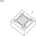
Fig. 1 is a perspective view of a known acoustic sensor fabricated using the MEMS technology. -
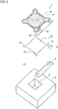
Fig. 2 is an exploded perspective view of the known acoustic sensor showing its internal structure. -
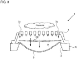
Fig. 3 is a diagram describing an acoustic sensor to which an excessively high pressure is abruptly applied. -
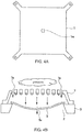
Figs. 4A and 4B are diagrams describing a known response to an excessively high pressure abruptly applied to the acoustic sensor. -
Figs. 5A and 5B are diagrams describing another known response to an excessively high pressure abruptly applied to the acoustic sensor. -
Figs. 6A and 6B are diagrams describing the functions of a pressure relief hole and a protrusion in the known response to an excessively high pressure abruptly applied to the acoustic sensor. -
Figs. 7A and 7B are diagrams describing the functions of a pressure relief hole and a protrusion in the known response to an excessively high pressure abruptly applied to the acoustic sensor. -
Figs. 8A and 8B are diagrams describing the functions of a pressure relief hole and a protrusion according to a first embodiment of the present invention. -
Figs. 9A to 9C are first diagrams describing the process of forming a pressure relief hole and a protrusion according to the first embodiment of the present invention. -
Figs. 10A to 10C are second diagrams describing the process of forming the pressure relief hole and the protrusion according to the first embodiment of the present invention. -
Figs. 11A to 11C are third diagrams describing the process of forming a pressure relief hole and a protrusion according to the first embodiment of the present invention. -
Figs. 12A to 12C are fourth diagrams describing the process of forming the pressure relief hole and the protrusion according to the first embodiment of the present invention. -
Figs. 13A to 13C are fifth diagrams describing the process of forming a pressure relief hole and a protrusion according to the first embodiment of the present invention. -
Fig. 14 is a cross-sectional view showing a protrusion formed on a back plate and a pressure relief hole formed in a vibration electrode film according to a second embodiment. -
Figs. 15A and 15B are cross-sectional views showing a protrusion formed on a back plate and a pressure relief hole formed in a vibration electrode film according to a third embodiment. -
Fig. 16 is a cross-sectional view showing the protrusion formed on the back plate and the pressure relief hole formed in the vibration electrode film according to the third embodiment, for describing the function of a stopper formed on the back plate. -
Fig. 17 is a cross-sectional perspective view showing a protrusion formed on a back plate and a pressure relief hole formed in a vibration electrode film according to a fourth embodiment. -
Figs. 18A and 18B are diagrams describing the functions of the protrusion on the back plate and the pressure relief hole in the vibration electrode film according to the fourth embodiment. -
Figs. 19A to 19C are diagrams describing the process of forming a protrusion on a back plate and a pressure relief hole in a vibration electrode film according to the fourth embodiment. -
Fig. 20 is a second diagram describing the process of forming the protrusion on the back plate and the pressure relief hole in the vibration electrode film according to the fourth embodiment. - Embodiments of the present invention will now be described with reference to the drawings. The embodiments described below are mere examples of this invention and should not be construed as limiting the technical scope of the invention. Although the present invention is applicable to any electrostatic transducer, an electrostatic transducer used as an acoustic sensor will be described. However, a voice transducer according to the embodiments of the present invention may be used as any non-acoustic sensor for detecting the displacement of a vibration electrode film. For example, the transducer may be used as a pressure sensor, an acceleration sensor, or an inertial sensor. In addition, the transducer may be used as a non-sensor device such as a speaker for converting an electrical signal into a displacement. The components including a back plate, a vibration electrode film, a back chamber, and a substrate may be in any arrangement that provides the same functions as produced by the components arranged in the arrangement described below. For example, the back plate and the vibration electrode film may be reversed.
-
Fig. 1 is a perspective view of a knownacoustic sensor 1 fabricated using the micro electro mechanical system (MEMS) technology.Fig. 2 is an exploded perspective view of theacoustic sensor 1 showing its internal structure. Theacoustic sensor 1 is a laminate of a silicon substrate (substrate) 3 having aback chamber 2, and adielectric film 4, a vibration electrode film (diaphragm) 5, and a back plate 7 placed on the top surface of thesilicon substrate 3. The back plate 7 includes a fixedplate 6 and a fixedelectrode film 8 on the fixedplate 6 and adjacent to thesilicon substrate 3. The fixedplate 6 in the back plate 7 has multiple sound holes or openings across it (the individual sound holes are indicated by the dots in the shaded area of the fixedplate 6 shown inFigs. 1 and2 ). The fixedelectrode film 8 has a fixedelectrode pad 10 for obtaining an output signal arranged at one of its four corners. - The
silicon substrate 3 may be formed from, for example, single-crystal silicon. Thevibration electrode film 5 may be formed from, for example, conductive polycrystalline silicon. Thevibration electrode film 5 is thin and substantially rectangular, and hasfixation parts 12 at the four corners of a substantiallyquadrilateral vibration part 11. Thevibration electrode film 5 is located on the top surface of thesilicon substrate 3 to cover theback chamber 2, and is fixed to thesilicon substrate 3 at the fourfixation parts 12 serving as anchor portions. Thevibration part 11 of thevibration electrode film 5 vibrates vertically in response to sound pressure. - The
vibration electrode film 5 is not in contact with thesilicon substrate 3 nor with the back plate 7 except at its fourfixation parts 12. Thevibration electrode film 5 can thus vertically vibrate more smoothly in response to sound pressure. Thevibration part 11 has a vibrationfilm electrode pad 9 at one of thefixation parts 12 at the four corners. The fixedelectrode film 8 on the back plate 7 corresponds to the vibration area of thevibration electrode film 5, which is the area excluding thefixation parts 12 at the four corners. Thefixation parts 12 of thevibration electrode film 5 at the four corners do not vibrate in response to sound pressure and thus the capacitance remains unchanged between thevibration electrode film 5 and the fixedelectrode film 8. - When the
acoustic sensor 1 receives sound, the sound passes through the sound holes and applies sound pressure to thevibration electrode film 5. More specifically, the sound holes allow the sound pressure to be applied to thevibration electrode film 5. The sound holes also reduce thermal noise and thus reduce noise by allowing easy escape of air from the air gap between the back plate 7 and thevibration electrode film 5. - When the
acoustic sensor 1 with the structure described above receives sound, thevibration electrode film 5 vibrates to change the distance between thevibration electrode film 5 and the fixedelectrode film 8. In response to the change in the distance between thevibration electrode film 5 and the fixedelectrode film 8, the capacitance between thevibration electrode film 5 and the fixedelectrode film 8 changes. The sound pressure can be detected as an electrical signal by applying a direct current (DC) voltage across the vibrationfilm electrode pad 9 electrically connected to thevibration electrode film 5 and the fixedelectrode pad 10 electrically connected to the fixedelectrode film 8, and converting the resulting change in the capacitance into an electrical signal. - The above
acoustic sensor 1 known in the art may have the disadvantage described below.Fig. 3 is a schematic diagram showing theacoustic sensor 1 under an excessively high pressure. As shown inFig. 3 , when theacoustic sensor 1 receives an excessively high pressure, the large pressure may be applied to thevibration part 11 of thevibration electrode film 5 throughsound holes 7a formed in the back plate 7. The large pressure may severely distort thevibration part 11 and break thevibration electrode film 5. This disadvantage may occur when, for example, theacoustic sensor 1 receives an excessive air pressure or when theacoustic sensor 1 falls. -
Figs. 4A and 4B show a possible response to this. As shown inFig. 4A , ahole 5a for relieving an applied pressure is formed in thevibration electrode film 5. As shown inFig. 4B , an excessively high pressure applied through thesound holes 7a formed in the back plate 7 of theacoustic sensor 1 may be relieved through thehole 5a. This prevents thevibration electrode film 5 from breaking. However, although thehole 5a, which is normally open, formed in thevibration electrode film 5 improves the durability against pressure, the hole may reduce sensitivity, or may cause roll-off, particularly within a low-frequency sound range, and may degrade the frequency characteristics of theacoustic sensor 1. - Another response may be a vibration electrode film, and a plug portion separated from the vibration electrode film by slits included as a pressure relief measure. The plug portion may be held by a support on a back plate at the same level as the other part of the vibration electrode film. This vibration electrode film moves in accordance with the pressure difference across the film to enlarge the flow channel between the film and the plug portion, and the enlarged channel allows an excessively high pressure to be relieved (refer to, for example, Patent Literature 2).
- However, this response has disadvantages described below. For example, the plug portion is fragile because it is a part of the very thin vibration electrode film. The lid-like plug portion is supported on the back plate using the support that is a separate rod member. This complicates the manufacturing processes, and may cause the plug portion to come off the support.
- Further, this vibration electrode film moves in accordance with the pressure difference across the film to enlarge the flow channel between the vibration electrode film and the plug portion, which is separated from the vibration electrode film by the slits. The enlarged channel then allows an excessively high pressure to be relieved. More specifically, the flow channel corresponds to the gap between the thin films, which are the vibration electrode film and the plug portion separated from the vibration electrode film by the slits. Thus, when the amplitude of the vibration electrode film increases under a relatively large pressure, which is within an operable pressure range, the plug portion and the vibration electrode film may deviate from each other beyond their film thickness. The resulting larger flow channel may cause unstable frequency characteristics of the
acoustic sensor 1. - Another response to the above disadvantage is a vibration electrode film having holes for relieving an applied pressure. Before the vibration electrode film deforms, a column integral with and protruding from a back plate passes through and partially blocks the hole. When the vibration electrode film deforms under pressure, the relative movement between the vibration electrode film and the back plate withdraws the back plate column from the hole to uncover the entire hole, through which the pressure applied to the vibration electrode film is relieved.
-
Figs. 5A and 5B are schematic views of an acoustic sensor showing a part avibration electrode film 15 and aback plate 17 in the above structure.Fig. 5A is a plan view of thevibration electrode film 15.Fig. 5B is a cross-sectional view taken along line B-B', showing thevibration electrode film 15, theback plate 17, and asubstrate 13. As shown inFig. 5A ,pressure relief holes 15b are opened at the four corners of avibration part 21 of thevibration electrode film 15 in this structure. As shown inFig. 5B , acolumnar protrusion 17b integral with theback plate 17 passes through and blocks thepressure relief hole 15b before thevibration electrode film 15 receives an excessively high pressure. Theprotrusion 17b is a part of theback plate 17 that is formed when theback plate 17 is prepared through semiconductor manufacturing processes. - The functions of the
pressure relief holes 15b and theprotrusions 17b will now be described with reference toFigs. 6A and 6B. Fig. 6A shows the structure in which thevibration electrode film 15 has yet to receive an excessively high pressure.Fig. 6B shows the structure in which thevibration electrode film 15 has received an excessively high pressure and deformed greatly. As shown inFig. 6A , before thevibration electrode film 15 deforms, eachprotrusion 17b on theback plate 17 passes through and blocks the correspondingpressure relief hole 15b in thevibration electrode film 15. In this state, when pressure is applied to thevibration electrode film 15 from across theback plate 17, thepressure relief hole 15b allows less air to pass, and insufficiently relieves pressure. - However, when an excessively high pressure is applied to the
vibration electrode film 15, the pressure greatly deforms thevibration electrode film 15 away from theback plate 17 as shown inFig. 6B . This causes theprotrusion 17b to withdraw from thepressure relief hole 15b (the protrusion to no longer pass through the hole) and uncover thepressure relief hole 15b. The air applying the pressure to thevibration electrode film 15 passes through thepressure relief hole 15b downward in the figures. This instantaneously relieves the pressure applied to thevibration electrode film 15. The pressure relief prevents thevibration electrode film 15 from deforming further after theprotrusion 17b withdraws from thepressure relief hole 15b, thus preventing thevibration electrode film 15 from breaking. -
Figs. 7A and 7B show an example of the above structure including a steplessly and linearly taperedprotrusion 27b. In this structure, when avibration electrode film 25 deforms greatly under an excessively high pressure applied to thevibration electrode film 25, a more distal, small-diameter part of theprotrusion 27b passes through apressure relief hole 25b. This increases the area of air passage for relieving pressure, and prevents thevibration electrode film 25 from deforming excessively. - The known structures described above allow a successful pressure relief when receiving pressure from above (or from across the back plate) to move the vibration electrode film downward. However, when receiving pressure applied from below to move the vibration electrode film upward, the structures cannot increase the area of air passage for pressure relief, and thus cannot prevent the vibration electrode film from deforming excessively upward.
- When, for example, the
vibration electrode film 25 moves upward as shown inFig. 8A in the structure with the steplessly and linearly taperedprotrusion 27b, the area of air passage for pressure relief is reduced on the contrary. This structure cannot prevent thevibration electrode film 25 from deforming excessively upward. - In the present embodiment, the cross-sectional area of a
protrusion 37b parallel to aback plate 37 decreases steplessly and linearly toward the base, or theback plate 37, as shown inFig. 8B . When an excessively high pressure is applied to avibration electrode film 35 from below to greatly deform thevibration electrode film 35 upward, a smaller cross-section portion of theprotrusion 37b adjacent to the base passes through apressure relief hole 35b. This increases the area of air passage for pressure relief to prevent thevibration electrode film 35 from deforming excessively. - In the present embodiment, when an excessively high pressure is applied to the
vibration electrode film 35 from above (or from across the back plate 37) to greatly deform thevibration electrode film 35 downward, a larger cross-section portion of theprotrusion 37b adjacent to the distal end passes through thepressure relief hole 35b. This first reduces the area of air passage for pressure relief, but then increases the area of air passage sufficiently for pressure relieve at the position where theprotrusion 37b protrudes out of thepressure relief hole 35b in thevibration electrode film 35. The structure according to the present embodiment prevents thevibration electrode film 35 from deforming excessively under an excessively high pressure applied to thevibration electrode film 35 either from above or below. - The process of forming a protrusion and a pressure relief hole in the present embodiment will now be described with reference to
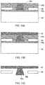
Figs. 9A to 10C . As shown inFig. 9A , a silicon oxide (SiO2)insulator layer 44a is first formed on the surface of a silicon (Si)substrate 43, and a polysilicon (poly-Si)film 45 to be a vibration electrode film is formed on theinsulator layer 44a. The poly-Si film 45 to be the vibration electrode film is then partially removed by etching to define apressure relief hole 45b. - As shown in
Fig. 9B , a silicon nitride (SiN)film 46 to form a protrusion is then formed on the poly-Si film 45. As shown inFig. 9C , theSiN film 46 is partially removed by etching with a photoresist to leave a part to be aprotrusion 47b. The vertical directivity of the etching may be reduced to provide a tapered shape. - As shown in
Fig. 10A , a SiO2sacrificial layer 44b is then formed. Theprotrusion 47b of SiN is embedded in SiO2 through smoothing such as chemical-mechanical polishing (CMP). As shown inFig. 10B , a SiN film to be aback plate 47 including the reverse taperedprotrusion 47b is then formed. - Subsequently, the
Si substrate 43 is removed by etching as in the process of fabricating a common acoustic sensor, and theSiO2 insulator layer 44a and thesacrificial layer 44b are removed by etching with hydrogen fluoride (HF) to complete theback plate 47 including theprotrusion 47b and thevibration electrode film 45 having thepressure relief hole 45b as shown inFig. 10C . - A second example of the process of forming a protrusion and a pressure relief hole in the present embodiment will now be described with reference to
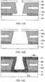
Figs. 11A to 12C . As shown inFig. 11A , a phospho-silicate glass (PSG) (phosphorus-containing SiO2 film 53) is first formed on the surface of aSi substrate 52, and a non-doped silicate glass (NSG) 54a, which is a SiO2 film free of impurities, is formed on thefilm 53. A poly-Si film 55 to be a vibration electrode film further formed on theNSG 54a. Thefilm 55 is partially removed by etching to form apressure relief hole 55b. Additionally, anNSG 54b is formed on this structure. - As shown in
Fig. 11B , a photoresist having an opening for a protrusion is then formed on theNSG 54a, and a part of theNSGs PSG 53 to uncover the surface of theSi substrate 52 as shown inFig. 11C . - As shown in
Fig. 12A , thePSG film 53 has an etching rate several times higher than theNSG films NSG films NSG films Fig. 12B , which is reverse to the taper inFig. 12A . - As shown in
Fig. 12C , the photoresist is then removed and a SiN film to be aback plate 57 and aprotrusion 57b is formed. Thus, theback plate 57 including the reverse taperedprotrusion 57b is obtained. - In the present embodiment, the
PSG film 53 and theNSG films - A third example of the process of forming a protrusion and a pressure relief hole in the present embodiment will now be described with reference to
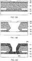
Figs. 13A to 13C . As shown inFig. 13A , a PSG film (phosphorus-containing SiO2 film 64) is first formed on the surface of aSi substrate 63. A poly-Si film 65 to be a vibration electrode film is further formed on thefilm 64. Thefilm 64 is partially removed by etching to form apressure relief hole 65b. Additionally, anNSG film 66, which is a SiO2 film free of impurities, is formed on thefilm 65b. A PSG film (phosphorus-containing SiO2 film 68) is further formed on theNSG film 66, and aphotoresist 69 having an opening for a protrusion is formed on the PSG film. - As shown in
Fig. 13B , the part corresponding to the protrusion is then removed from the PSG films (phosphorus-containingSiO2 films 64 and 68) and theNSG film 66 by etching with an aqueous HF solution. In this etching, the difference in the etching rates between the layers allows the slope to be modified variously. The etching with the aqueous HF solution also removes thePSG film 64 to uncover the surface of theSi substrate 63. - As shown in
Fig. 13C , the photoresist is then removed before a silicon nitride (SiN) film to be aback plate 67 and aprotrusion 67b is placed to form theback plate 67 including the reverse taperedprotrusion 67b. - The
PSG film 68, which is the uppermost layer in the present embodiment, may be eliminated. The surface on which thephotoresist 69 is placed can typically have a locally higher etching rate. With this tendency of the etching rate, the similar shape as in the above embodiment can be formed without thePSG film 68. - The
protrusion 67b in the present embodiment has its part adjacent to theback plate 67 with a horizontal cross-sectional area at least smaller than the average corresponds to a predetermined position of the present invention. Theprotrusion 67b has its part with a horizontal cross-sectional area at least smaller than the average corresponds to a smaller cross-section portion. - A second embodiment of the present invention will now be described. In the present embodiment, a sound hole is formed in a substantially columnar protrusion integral with a back plate. The sound hole includes the side surface of the protrusion in the horizontal direction, and extends in the protrusion halfway in the vertical direction. This sound hole increases the area of the pressure relief channel adjacent to the base of the protrusion.
-
Fig. 14 is a cross-sectional view showing aprotrusion 77b formed on aback plate 77 and apressure relief hole 75b formed in avibration electrode film 75 according to the present embodiment. Theprotrusion 77b in the present embodiment, which is substantially columnar, is formed with the sound hole in theback plate 77 by etching. More specifically, acavity 77c is formed to include the side surface of thecolumnar protrusion 77b in the horizontal direction and extend in thecolumnar protrusion 77b halfway in the vertical direction, while leaving a distal end portion of theprotrusion 77b. - The
cavity 77c and the adjacent side surface of theprotrusion 77b define anopening 77d. Theopening 77d is formed on the side surface of theprotrusion 77b and is adjacent to theback plate 77. In the state shown inFig. 14 , under an excessively high pressure applied to thevibration electrode film 75 from its side opposite to the back plate 77 (from the bottom of the drawing), thevibration electrode film 75 deforms toward the back plate 77 (toward the top in the figure). When thevibration electrode film 75 further deforms toward theback plate 77 beyond the lower end of theopening 77d, the air applying the pressure to thevibration electrode film 75 enters theopening 77d, passes through thecavity 77c, and escapes from the top of theback plate 77. This escaping air relieves the pressure applied to thevibration electrode film 75 from its side opposite to theback plate 77. - In this manner, the
cavity 77c can be formed to include the side surface of theprotrusion 77b as viewed from above in the process of forming a sound hole in theback plate 77 having theprotrusion 77b. This easily reduces the cross-sectional area of a part of theprotrusion 77b adjacent to theback plate 77. The part of theprotrusion 77b in the height direction formed as thecavity 77c corresponds to a predetermined position of the present invention. The part of theprotrusion 77b formed as thecavity 77c corresponds to a smaller cross-section portion. - A third embodiment of the present invention will now be described. In the present embodiment, a tapered protrusion that decreases its diameter from a back plate toward the distal end has an opening in a part of the side surface adjacent to the back plate, and a cavity extending through the opening and the top of the back plate.
-
Figs. 15A and 15B show the function of a known tapered protrusion that decreases its diameter from a back plate toward the distal end, and the function of such a protrusion having an opening in a part of the side surface adjacent to the back plate and a cavity extending through the opening and the top of the back plate. -
Fig. 15A shows a typical tapered protrusion.Fig. 15B shows a tapered protrusion having such an opening and a cavity extending through the opening and the top of the back plate. In the structure having a typical taperedprotrusion 87b as shown inFig. 15A , avibration electrode film 85 deforms toward theback plate 87 under an excessively high pressure applied to thevibration electrode film 85 from its side opposite to aback plate 87. As thevibration electrode film 85 deforms more toward theback plate 87, the area of the gap between theprotrusion 87b and apressure relief hole 85b decreases, causing difficulties in relieving the pressure. - In contrast, as shown in
Fig. 15B , the tapered protrusion having anopening 87d in a part adjacent to theback plate 87, and acavity 87c extending through theopening 87d and the top of theback plate 87 shows a different behavior. Under an excessively high pressure applied to thevibration electrode film 85 from its side opposite to theback plate 87, thevibration electrode film 85 deforms toward theback plate 87. However, when thevibration electrode film 85 reaches the position corresponding to theopening 87d, the air applying the pressure to thevibration electrode film 85 escapes from the top of theback plate 87 through theopening 87d and thecavity 87c. - Thus, the pressure applied to the
vibration electrode film 85 can be relieved at this position. The pressure relief prevents thevibration electrode film 85 from deforming further. In the present embodiment, any foreign matter contained in the air applying the pressure to thevibration electrode film 85 from its side opposite to theback plate 87 can be removed through theopening 87d and thecavity 87c, preventing foreign matter from being stuck or accumulating between or near theprotrusion 87b and thepressure relief hole 85b. - The structure in the present embodiment may include a
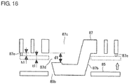
stopper 87e on theback plate 87 as shown inFig. 16 . Thestopper 87e typically prevents adhesion between theback plate 87 and thevibration electrode film 85, or prevents short circuiting due to contact between them. In the present embodiment, the condition below is satisfied:
stopper 87e, d1 is the depth of theopening 87d from theback plate 87, and t1 is the thickness of thevibration electrode film 85. - Although the
vibration electrode film 85 toward theback plate 87 under an excessively high pressure applied to thevibration electrode film 85 from its side opposite to theback plate 87, thevibration electrode film 85 comes into contact with thestopper 87e on theback plate 87 and then stabilizes. In this state, a part of theopening 87d reliably communicates with the side of thevibration electrode film 85 opposite to theback plate 87. Thus, when an excessively high pressure is applied to thevibration electrode film 85 from its side opposite to theback plate 87, the air may escape from the top of theback plate 87 through theopening 87d and thecavity 87c in a more reliable manner to relieve the pressure applied to thevibration electrode film 85. Although the lower end of theopening 87d is flush with the bottom of the inner wall of theprotrusion 87b inFig. 15 , the lower end of theopening 87d may not be flush with the bottom of the inner wall of theprotrusion 87b. As shown inFig. 16 , they may be different levels. - Although the
stopper 87e extends from theback plate 87 in the present embodiment, a protrusion functioning as a stopper may extend from thevibration electrode film 85. This protrusion may be formed as a part of thevibration electrode film 85 or adding another member on the top of thevibration electrode film 85. The protrusion may prevent adhesion to theback plate 87 in the same manner as thestopper 87e. With the height h1 of the stopper, the depth d1 of the opening from back plate, and the thickness t1 of the vibration electrode film satisfying condition (1), the present embodiment produces its advantages. - A fourth embodiment of the present invention will now be described. In the present embodiment, a vibration electrode film has a slit pressure relief hole, and a back plate has a flat protrusion, instead of a columnar or tapered protrusion. The flat protrusion can be placed through the pressure relief hole.
-
Fig. 17 is a cross-sectional perspective view of aback plate 97, aprotrusion 97b, avibration electrode film 95, and apressure relief hole 95b according to the present embodiment. As described in the above embodiment, thepressure relief hole 95b is not circular but is a slit as viewed from above. Theprotrusion 97b is flat and can be inserted into the slitpressure relief hole 95b. InFig. 17 , thevibration electrode film 95 and theback plate 97 are sectioned along the middle of the slitpressure relief hole 95b and theflat protrusion 97b. The slitpressure relief hole 95b and theflat protrusion 97b, which are narrow, allow theback plate 97 to be easily flat in semiconductor manufacturing processes. Theflat back plate 97 has lower stress concentration. For example, the slit with a width not more than twice the distance between thevibration electrode film 95 and theback plate 97 allows theback plate 97 to be easily flat. - In the present embodiment, the process of forming a
sound hole 97a in theback plate 97 also involves forming acavity 97c extending in theflat protrusion 97b halfway in the height direction. Anopening 97d formed in this manner is continuous to the right and left sides of theflat protrusion 97b. In the present embodiment, thesound hole 97a and thecavity 97c may be desirably circular as viewed from above. This structure prevents stress concentration on parts of theback plate 97, particularly near theflat protrusion 97b. -
Figs. 18A and 18B are diagrams describing the functions of theback plate 97 and thevibration electrode film 95 according to the present embodiment.Figs. 18A and 18B are cross-sectional views of theback plate 97 and thevibration electrode film 95 inFig. 17 as viewed in the direction of the normal to the sections. InFig. 18A , thevibration electrode film 95 is not deformed. InFig. 18B , thevibration electrode film 95 has been deformed toward theback plate 97 under an excessively high pressure applied to thevibration electrode film 95 from its side opposite to theback plate 97. - In the present embodiment, the
vibration electrode film 95 deforms toward theback plate 97 under an excessively high pressure applied to thevibration electrode film 95 from its side opposite to theback plate 97. In this state, the air applying the pressure to thevibration electrode film 95 can enter theopening 97d continuous to the right and left sides of theflat protrusion 97b, pass through thecavity 97c, and escape toward the top of theback plate 97. This relieves the pressure applied to thevibration electrode film 95 to prevent thevibration electrode film 95 from deforming excessively. - In the present embodiment, when the
vibration electrode film 95 greatly deforms away from theback plate 97 under an excessively high pressure applied from across theback plate 97, theflat protrusion 97b withdraws from the slitpressure relief hole 95b in thevibration electrode film 95 to enable air to pass through the entirepressure relief hole 95b. Thus, the area of air passage is large enough to relieve the pressure applied to thevibration electrode film 95. The structure according to the present embodiment thus prevents the vibration electrode film from deforming excessively 95 under an excessively high pressure applied to thevibration electrode film 95 from either above or below. - The process of forming a protrusion and a pressure relief hole in the present embodiment will now be described with reference to
Figs. 19A to 19C . As shown inFig. 19A , aSiO2 insulator layer 104a is first formed on the surface of aSi substrate 103, and a poly-Si film 105 to be a vibration electrode film is formed on theinsulator layer 104a. The poly-Si film 105 is then partially removed by etching to define apressure relief hole 105b. Additionally, a SiO2sacrificial layer 104b is formed on the poly-Si film 105, and a slit area to be the protrusion is removed by etching from theinsulator layer 104a and thesacrificial layer 104b. - As shown in
Fig. 19B , a poly-Si film 106 to be a fixed electrode film is then formed. Additionally,SiN films SiO2 insulator layer 104a and the SiO2sacrificial layer 104b, in which theSiN film 107b to be the protrusion is formed, has a narrow width. Thus, when theback plate 107 is formed, the slit is filled with the SiN film, and theprotrusion 107b finally becomes flat. Then,sound holes 107a and acavity 107c above theprotrusion 107b are formed by etching. As shown inFig. 19C , theSi substrate 103, theinsulator layer 104a, and thesacrificial layer 104b are then removed by etching, leaving the portions to be theback plate 107 and theprotrusion 107b, and thevibration electrode film 105. As a result, theprotrusion 107b on theback plate 107 and thepressure relief hole 105b in thevibration electrode film 105 are obtained. - In the present embodiment, as shown in
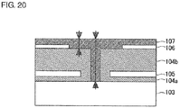
Fig. 20 , the portion to be theflat protrusion 107b is thick in the vertical direction. When thesound holes 107a and thecavity 107c above theprotrusion 107b are simultaneously formed by etching with high vertical directivity, such as dry etching, the film is left only at the distal end of theprotrusion 107b. This allows easy fabrication of the structure with a cavity formed in theprotrusion 107b adjacent to theback plate 107. This method of fabrication is optional. Thesound holes 107a and thespace 107c above theprotrusion 107b may also be etched separately. The side surface of theprotrusion 107b may be upright or tapered (sloped). The portion to be theflat protrusion 107b having an upright side surface is thick in the vertical direction, and thus allows easy etching. -
- 1
- acoustic sensor
- 2
- back chamber
- 3, 13, 43, 52, 63
- (silicon) substrate
- 5, 15, 25, 35, 45, 55, 65, 75, 85, 95, 105
- vibration electrode film
- 7, 17, 27, 37, 47, 57, 67, 77, 87, 97, 107
- back plate
- 15b, 25b, 35b, 45b, 55b, 65b, 75b, 85b, 95b, 105b
- pressure relief hole
- 17b, 27b, 37b, 47b, 57b, 67b, 77b, 87b, 97b, 107b
- protrusion
Claims (3)
- A capacitive transducer, comprising:a substrate having an opening in a surface thereof;a back plate (37) facing the opening in the substrate;a vibration electrode film (35) facing the back plate (37) across a space, the vibration electrode film (35) being deformable to have a deformation converted into a change in capacitance between the vibration electrode film (35) and the back plate (37), the vibration electrode film (35) having a through-hole as a pressure relief hole (35b); anda protrusion (37b) integral with and formed from the same member as the back plate, the protrusion (37b) being placeable in the pressure relief hole (35b) before the vibration electrode film (35) deforms,wherein the protrusion (37b) and the pressure relief hole (35b) have a gap therebetween defining an airflow channel as a pressure relief channel, andthe protrusion (37b) includes, at a predetermined position adjacent to the back plate, a smaller cross-section portion having a smaller cross-sectional area in a direction parallel to the back plate (37) than a portion of the protrusion (37b) more distal from the predetermined position.
- The capacitive transducer according to claim 1, wherein
the protrusion (37b) is tapered to have a cross-sectional area decreasing toward the back plate. - An acoustic sensor (1) comprising:the capacitive transducer according claim 1 or 2,the acoustic sensor (1) being configured to convert a sound pressure into a change in capacitance between the vibration electrode film (35) and the back plate (37), and detect the sound pressure.
Applications Claiming Priority (2)
| Application Number | Priority Date | Filing Date | Title |
|---|---|---|---|
| JP2016047305A JP6658126B2 (en) | 2016-03-10 | 2016-03-10 | Capacitive transducer and acoustic sensor |
| PCT/JP2017/003354 WO2017154414A1 (en) | 2016-03-10 | 2017-01-31 | Capacitive transducer and acoustic sensor |
Publications (3)
| Publication Number | Publication Date |
|---|---|
| EP3328096A1 EP3328096A1 (en) | 2018-05-30 |
| EP3328096A4 EP3328096A4 (en) | 2019-02-27 |
| EP3328096B1 true EP3328096B1 (en) | 2020-04-01 |
Family
ID=59789230
Family Applications (1)
| Application Number | Title | Priority Date | Filing Date |
|---|---|---|---|
| EP17762760.1A Active EP3328096B1 (en) | 2016-03-10 | 2017-01-31 | Capacitive transducer and acoustic sensor |
Country Status (5)
| Country | Link |
|---|---|
| US (1) | US10440481B2 (en) |
| EP (1) | EP3328096B1 (en) |
| JP (1) | JP6658126B2 (en) |
| CN (1) | CN107852559B (en) |
| WO (1) | WO2017154414A1 (en) |
Families Citing this family (4)
| Publication number | Priority date | Publication date | Assignee | Title |
|---|---|---|---|---|
| CN107509150B (en) * | 2017-09-29 | 2020-06-09 | 瑞声声学科技(深圳)有限公司 | MEMS microphone |
| DE102020113974A1 (en) * | 2019-05-28 | 2020-12-03 | Apple Inc. | VENTED ACOUSTIC TRANSDUCERS AND RELATED PROCEDURES AND SYSTEMS |
| TWI770543B (en) * | 2020-06-29 | 2022-07-11 | 美律實業股份有限公司 | Microphone structure |
| KR102350898B1 (en) * | 2020-10-19 | 2022-01-14 | (주)다빛센스 | Method for forming mems electrode |
Family Cites Families (10)
| Publication number | Priority date | Publication date | Assignee | Title |
|---|---|---|---|---|
| JP2008259061A (en) * | 2007-04-06 | 2008-10-23 | Matsushita Electric Works Ltd | Electrostatic transducer |
| JP5400708B2 (en) | 2010-05-27 | 2014-01-29 | オムロン株式会社 | Acoustic sensor, acoustic transducer, microphone using the acoustic transducer, and method of manufacturing the acoustic transducer |
| DE102012212112A1 (en) * | 2012-07-11 | 2014-01-30 | Robert Bosch Gmbh | Component with a micromechanical microphone structure |
| GB2506174A (en) * | 2012-09-24 | 2014-03-26 | Wolfson Microelectronics Plc | Protecting a MEMS device from excess pressure and shock |
| ITTO20130441A1 (en) * | 2013-05-30 | 2014-12-01 | St Microelectronics Srl | DETECTION STRUCTURE FOR A MEMS ACOUSTIC TRANSDUCER WITH IMPROVED DEFORMATION RESISTANCE |
| KR101614330B1 (en) * | 2013-08-06 | 2016-04-21 | 고어텍 인크 | An anti-impact silicon based mems microphone, a system and a package with the same |
| JP6179297B2 (en) | 2013-09-13 | 2017-08-16 | オムロン株式会社 | Acoustic transducer and microphone |
| JP6149628B2 (en) * | 2013-09-13 | 2017-06-21 | オムロン株式会社 | Acoustic transducer and microphone |
| KR20150047046A (en) * | 2013-10-23 | 2015-05-04 | 삼성전기주식회사 | Acoustic transducer and package module |
| CN106688246B (en) * | 2015-03-12 | 2020-01-21 | 欧姆龙株式会社 | Capacitance type converter and acoustic sensor |
-
2016
- 2016-03-10 JP JP2016047305A patent/JP6658126B2/en active Active
-
2017
- 2017-01-31 CN CN201780002680.2A patent/CN107852559B/en active Active
- 2017-01-31 WO PCT/JP2017/003354 patent/WO2017154414A1/en active Application Filing
- 2017-01-31 US US15/753,521 patent/US10440481B2/en active Active
- 2017-01-31 EP EP17762760.1A patent/EP3328096B1/en active Active
Non-Patent Citations (1)
| Title |
|---|
| None * |
Also Published As
| Publication number | Publication date |
|---|---|
| CN107852559A (en) | 2018-03-27 |
| US10440481B2 (en) | 2019-10-08 |
| CN107852559B (en) | 2020-10-16 |
| EP3328096A1 (en) | 2018-05-30 |
| JP2017163408A (en) | 2017-09-14 |
| US20180249257A1 (en) | 2018-08-30 |
| JP6658126B2 (en) | 2020-03-04 |
| EP3328096A4 (en) | 2019-02-27 |
| WO2017154414A1 (en) | 2017-09-14 |
Similar Documents
| Publication | Publication Date | Title |
|---|---|---|
| EP3328096B1 (en) | Capacitive transducer and acoustic sensor | |
| EP3328095B1 (en) | Capacitive transducer and acoustic sensor | |
| US9986344B2 (en) | MEMS microphone with low pressure region between diaphragm and counter electrode | |
| KR101185291B1 (en) | Acoustic sensor and manufacturing method thereof | |
| EP2073272B1 (en) | Vibration sensor and method for manufacturing the vibration sensor | |
| EP2387255B1 (en) | Acoustic sensor and microphone | |
| US8415717B2 (en) | Acoustic sensor | |
| JP6332549B2 (en) | Capacitive transducer and acoustic sensor | |
| US20140225204A1 (en) | Acoustic sensor and method for manufacturing same | |
| US20110048138A1 (en) | Mems stress concentrating structure for mems sensors | |
| US10469957B2 (en) | Capacitive transducer and acoustic sensor | |
| JP4737535B2 (en) | Condenser microphone | |
| US20120189143A1 (en) | Micromechanical Microphone Device and Method for Producing a Micromechanical Microphone Device | |
| JP2009147798A (en) | Capacitor microphone and manufacturing method thereof |
Legal Events
| Date | Code | Title | Description |
|---|---|---|---|
| STAA | Information on the status of an ep patent application or granted ep patent |
Free format text: STATUS: THE INTERNATIONAL PUBLICATION HAS BEEN MADE |
|
| PUAI | Public reference made under article 153(3) epc to a published international application that has entered the european phase |
Free format text: ORIGINAL CODE: 0009012 |
|
| STAA | Information on the status of an ep patent application or granted ep patent |
Free format text: STATUS: REQUEST FOR EXAMINATION WAS MADE |
|
| 17P | Request for examination filed |
Effective date: 20180214 |
|
| AK | Designated contracting states |
Kind code of ref document: A1 Designated state(s): AL AT BE BG CH CY CZ DE DK EE ES FI FR GB GR HR HU IE IS IT LI LT LU LV MC MK MT NL NO PL PT RO RS SE SI SK SM TR |
|
| AX | Request for extension of the european patent |
Extension state: BA ME |
|
| A4 | Supplementary search report drawn up and despatched |
Effective date: 20190129 |
|
| RIC1 | Information provided on ipc code assigned before grant |
Ipc: H01L 29/84 20060101ALI20190123BHEP Ipc: H04R 19/04 20060101AFI20190123BHEP Ipc: B81B 3/00 20060101ALI20190123BHEP Ipc: H04R 19/00 20060101ALI20190123BHEP |
|
| DAV | Request for validation of the european patent (deleted) | ||
| DAX | Request for extension of the european patent (deleted) | ||
| GRAP | Despatch of communication of intention to grant a patent |
Free format text: ORIGINAL CODE: EPIDOSNIGR1 |
|
| STAA | Information on the status of an ep patent application or granted ep patent |
Free format text: STATUS: GRANT OF PATENT IS INTENDED |
|
| INTG | Intention to grant announced |
Effective date: 20191023 |
|
| GRAS | Grant fee paid |
Free format text: ORIGINAL CODE: EPIDOSNIGR3 |
|
| GRAA | (expected) grant |
Free format text: ORIGINAL CODE: 0009210 |
|
| STAA | Information on the status of an ep patent application or granted ep patent |
Free format text: STATUS: THE PATENT HAS BEEN GRANTED |
|
| AK | Designated contracting states |
Kind code of ref document: B1 Designated state(s): AL AT BE BG CH CY CZ DE DK EE ES FI FR GB GR HR HU IE IS IT LI LT LU LV MC MK MT NL NO PL PT RO RS SE SI SK SM TR |
|
| REG | Reference to a national code |
Ref country code: GB Ref legal event code: FG4D |
|
| REG | Reference to a national code |
Ref country code: AT Ref legal event code: REF Ref document number: 1252914 Country of ref document: AT Kind code of ref document: T Effective date: 20200415 Ref country code: CH Ref legal event code: EP |
|
| REG | Reference to a national code |
Ref country code: DE Ref legal event code: R096 Ref document number: 602017014099 Country of ref document: DE |
|
| REG | Reference to a national code |
Ref country code: IE Ref legal event code: FG4D |
|
| PG25 | Lapsed in a contracting state [announced via postgrant information from national office to epo] |
Ref country code: BG Free format text: LAPSE BECAUSE OF FAILURE TO SUBMIT A TRANSLATION OF THE DESCRIPTION OR TO PAY THE FEE WITHIN THE PRESCRIBED TIME-LIMIT Effective date: 20200701 |
|
| REG | Reference to a national code |
Ref country code: NL Ref legal event code: MP Effective date: 20200401 |
|
| REG | Reference to a national code |
Ref country code: LT Ref legal event code: MG4D |
|
| PG25 | Lapsed in a contracting state [announced via postgrant information from national office to epo] |
Ref country code: GR Free format text: LAPSE BECAUSE OF FAILURE TO SUBMIT A TRANSLATION OF THE DESCRIPTION OR TO PAY THE FEE WITHIN THE PRESCRIBED TIME-LIMIT Effective date: 20200702 Ref country code: NO Free format text: LAPSE BECAUSE OF FAILURE TO SUBMIT A TRANSLATION OF THE DESCRIPTION OR TO PAY THE FEE WITHIN THE PRESCRIBED TIME-LIMIT Effective date: 20200701 Ref country code: CZ Free format text: LAPSE BECAUSE OF FAILURE TO SUBMIT A TRANSLATION OF THE DESCRIPTION OR TO PAY THE FEE WITHIN THE PRESCRIBED TIME-LIMIT Effective date: 20200401 Ref country code: FI Free format text: LAPSE BECAUSE OF FAILURE TO SUBMIT A TRANSLATION OF THE DESCRIPTION OR TO PAY THE FEE WITHIN THE PRESCRIBED TIME-LIMIT Effective date: 20200401 Ref country code: IS Free format text: LAPSE BECAUSE OF FAILURE TO SUBMIT A TRANSLATION OF THE DESCRIPTION OR TO PAY THE FEE WITHIN THE PRESCRIBED TIME-LIMIT Effective date: 20200801 Ref country code: PT Free format text: LAPSE BECAUSE OF FAILURE TO SUBMIT A TRANSLATION OF THE DESCRIPTION OR TO PAY THE FEE WITHIN THE PRESCRIBED TIME-LIMIT Effective date: 20200817 Ref country code: LT Free format text: LAPSE BECAUSE OF FAILURE TO SUBMIT A TRANSLATION OF THE DESCRIPTION OR TO PAY THE FEE WITHIN THE PRESCRIBED TIME-LIMIT Effective date: 20200401 Ref country code: NL Free format text: LAPSE BECAUSE OF FAILURE TO SUBMIT A TRANSLATION OF THE DESCRIPTION OR TO PAY THE FEE WITHIN THE PRESCRIBED TIME-LIMIT Effective date: 20200401 Ref country code: SE Free format text: LAPSE BECAUSE OF FAILURE TO SUBMIT A TRANSLATION OF THE DESCRIPTION OR TO PAY THE FEE WITHIN THE PRESCRIBED TIME-LIMIT Effective date: 20200401 |
|
| REG | Reference to a national code |
Ref country code: AT Ref legal event code: MK05 Ref document number: 1252914 Country of ref document: AT Kind code of ref document: T Effective date: 20200401 |
|
| PG25 | Lapsed in a contracting state [announced via postgrant information from national office to epo] |
Ref country code: HR Free format text: LAPSE BECAUSE OF FAILURE TO SUBMIT A TRANSLATION OF THE DESCRIPTION OR TO PAY THE FEE WITHIN THE PRESCRIBED TIME-LIMIT Effective date: 20200401 Ref country code: RS Free format text: LAPSE BECAUSE OF FAILURE TO SUBMIT A TRANSLATION OF THE DESCRIPTION OR TO PAY THE FEE WITHIN THE PRESCRIBED TIME-LIMIT Effective date: 20200401 Ref country code: LV Free format text: LAPSE BECAUSE OF FAILURE TO SUBMIT A TRANSLATION OF THE DESCRIPTION OR TO PAY THE FEE WITHIN THE PRESCRIBED TIME-LIMIT Effective date: 20200401 |
|
| PG25 | Lapsed in a contracting state [announced via postgrant information from national office to epo] |
Ref country code: AL Free format text: LAPSE BECAUSE OF FAILURE TO SUBMIT A TRANSLATION OF THE DESCRIPTION OR TO PAY THE FEE WITHIN THE PRESCRIBED TIME-LIMIT Effective date: 20200401 |
|
| REG | Reference to a national code |
Ref country code: DE Ref legal event code: R097 Ref document number: 602017014099 Country of ref document: DE |
|
| PG25 | Lapsed in a contracting state [announced via postgrant information from national office to epo] |
Ref country code: DK Free format text: LAPSE BECAUSE OF FAILURE TO SUBMIT A TRANSLATION OF THE DESCRIPTION OR TO PAY THE FEE WITHIN THE PRESCRIBED TIME-LIMIT Effective date: 20200401 Ref country code: ES Free format text: LAPSE BECAUSE OF FAILURE TO SUBMIT A TRANSLATION OF THE DESCRIPTION OR TO PAY THE FEE WITHIN THE PRESCRIBED TIME-LIMIT Effective date: 20200401 Ref country code: AT Free format text: LAPSE BECAUSE OF FAILURE TO SUBMIT A TRANSLATION OF THE DESCRIPTION OR TO PAY THE FEE WITHIN THE PRESCRIBED TIME-LIMIT Effective date: 20200401 Ref country code: EE Free format text: LAPSE BECAUSE OF FAILURE TO SUBMIT A TRANSLATION OF THE DESCRIPTION OR TO PAY THE FEE WITHIN THE PRESCRIBED TIME-LIMIT Effective date: 20200401 Ref country code: SM Free format text: LAPSE BECAUSE OF FAILURE TO SUBMIT A TRANSLATION OF THE DESCRIPTION OR TO PAY THE FEE WITHIN THE PRESCRIBED TIME-LIMIT Effective date: 20200401 Ref country code: RO Free format text: LAPSE BECAUSE OF FAILURE TO SUBMIT A TRANSLATION OF THE DESCRIPTION OR TO PAY THE FEE WITHIN THE PRESCRIBED TIME-LIMIT Effective date: 20200401 |
|
| PLBE | No opposition filed within time limit |
Free format text: ORIGINAL CODE: 0009261 |
|
| STAA | Information on the status of an ep patent application or granted ep patent |
Free format text: STATUS: NO OPPOSITION FILED WITHIN TIME LIMIT |
|
| PG25 | Lapsed in a contracting state [announced via postgrant information from national office to epo] |
Ref country code: PL Free format text: LAPSE BECAUSE OF FAILURE TO SUBMIT A TRANSLATION OF THE DESCRIPTION OR TO PAY THE FEE WITHIN THE PRESCRIBED TIME-LIMIT Effective date: 20200401 Ref country code: SK Free format text: LAPSE BECAUSE OF FAILURE TO SUBMIT A TRANSLATION OF THE DESCRIPTION OR TO PAY THE FEE WITHIN THE PRESCRIBED TIME-LIMIT Effective date: 20200401 |
|
| 26N | No opposition filed |
Effective date: 20210112 |
|
| PG25 | Lapsed in a contracting state [announced via postgrant information from national office to epo] |
Ref country code: SI Free format text: LAPSE BECAUSE OF FAILURE TO SUBMIT A TRANSLATION OF THE DESCRIPTION OR TO PAY THE FEE WITHIN THE PRESCRIBED TIME-LIMIT Effective date: 20200401 |
|
| PG25 | Lapsed in a contracting state [announced via postgrant information from national office to epo] |
Ref country code: MC Free format text: LAPSE BECAUSE OF FAILURE TO SUBMIT A TRANSLATION OF THE DESCRIPTION OR TO PAY THE FEE WITHIN THE PRESCRIBED TIME-LIMIT Effective date: 20200401 |
|
| REG | Reference to a national code |
Ref country code: CH Ref legal event code: PL |
|
| PG25 | Lapsed in a contracting state [announced via postgrant information from national office to epo] |
Ref country code: LU Free format text: LAPSE BECAUSE OF NON-PAYMENT OF DUE FEES Effective date: 20210131 |
|
| REG | Reference to a national code |
Ref country code: BE Ref legal event code: MM Effective date: 20210131 |
|
| PG25 | Lapsed in a contracting state [announced via postgrant information from national office to epo] |
Ref country code: LI Free format text: LAPSE BECAUSE OF NON-PAYMENT OF DUE FEES Effective date: 20210131 Ref country code: CH Free format text: LAPSE BECAUSE OF NON-PAYMENT OF DUE FEES Effective date: 20210131 |
|
| PG25 | Lapsed in a contracting state [announced via postgrant information from national office to epo] |
Ref country code: IE Free format text: LAPSE BECAUSE OF NON-PAYMENT OF DUE FEES Effective date: 20210131 |
|
| REG | Reference to a national code |
Ref country code: DE Ref legal event code: R081 Ref document number: 602017014099 Country of ref document: DE Owner name: MMI SEMICONDUCTOR CO., LTD., TAMA-SHI, JP Free format text: FORMER OWNER: OMRON CORPORATION, KYOTO, JP |
|
| PG25 | Lapsed in a contracting state [announced via postgrant information from national office to epo] |
Ref country code: BE Free format text: LAPSE BECAUSE OF NON-PAYMENT OF DUE FEES Effective date: 20210131 |
|
| PGFP | Annual fee paid to national office [announced via postgrant information from national office to epo] |
Ref country code: IT Payment date: 20221213 Year of fee payment: 7 |
|
| PG25 | Lapsed in a contracting state [announced via postgrant information from national office to epo] |
Ref country code: CY Free format text: LAPSE BECAUSE OF FAILURE TO SUBMIT A TRANSLATION OF THE DESCRIPTION OR TO PAY THE FEE WITHIN THE PRESCRIBED TIME-LIMIT Effective date: 20200401 |
|
| PG25 | Lapsed in a contracting state [announced via postgrant information from national office to epo] |
Ref country code: HU Free format text: LAPSE BECAUSE OF FAILURE TO SUBMIT A TRANSLATION OF THE DESCRIPTION OR TO PAY THE FEE WITHIN THE PRESCRIBED TIME-LIMIT; INVALID AB INITIO Effective date: 20170131 |
|
| PGFP | Annual fee paid to national office [announced via postgrant information from national office to epo] |
Ref country code: GB Payment date: 20231207 Year of fee payment: 8 |
|
| PGFP | Annual fee paid to national office [announced via postgrant information from national office to epo] |
Ref country code: FR Payment date: 20231212 Year of fee payment: 8 |
|
| PG25 | Lapsed in a contracting state [announced via postgrant information from national office to epo] |
Ref country code: MK Free format text: LAPSE BECAUSE OF FAILURE TO SUBMIT A TRANSLATION OF THE DESCRIPTION OR TO PAY THE FEE WITHIN THE PRESCRIBED TIME-LIMIT Effective date: 20200401 |
|
| PGFP | Annual fee paid to national office [announced via postgrant information from national office to epo] |
Ref country code: DE Payment date: 20231205 Year of fee payment: 8 |