WO2017154394A1 - Flash light source device - Google Patents
Flash light source device Download PDFInfo
- Publication number
- WO2017154394A1 WO2017154394A1 PCT/JP2017/002746 JP2017002746W WO2017154394A1 WO 2017154394 A1 WO2017154394 A1 WO 2017154394A1 JP 2017002746 W JP2017002746 W JP 2017002746W WO 2017154394 A1 WO2017154394 A1 WO 2017154394A1
- Authority
- WO
- WIPO (PCT)
- Prior art keywords
- housing
- electromagnetic shield
- opening
- light source
- source device
- Prior art date
Links
Images


Classifications
-
- F—MECHANICAL ENGINEERING; LIGHTING; HEATING; WEAPONS; BLASTING
- F21—LIGHTING
- F21S—NON-PORTABLE LIGHTING DEVICES; SYSTEMS THEREOF; VEHICLE LIGHTING DEVICES SPECIALLY ADAPTED FOR VEHICLE EXTERIORS
- F21S10/00—Lighting devices or systems producing a varying lighting effect
- F21S10/06—Lighting devices or systems producing a varying lighting effect flashing, e.g. with rotating reflector or light source
-
- F—MECHANICAL ENGINEERING; LIGHTING; HEATING; WEAPONS; BLASTING
- F21—LIGHTING
- F21V—FUNCTIONAL FEATURES OR DETAILS OF LIGHTING DEVICES OR SYSTEMS THEREOF; STRUCTURAL COMBINATIONS OF LIGHTING DEVICES WITH OTHER ARTICLES, NOT OTHERWISE PROVIDED FOR
- F21V23/00—Arrangement of electric circuit elements in or on lighting devices
- F21V23/003—Arrangement of electric circuit elements in or on lighting devices the elements being electronics drivers or controllers for operating the light source, e.g. for a LED array
- F21V23/004—Arrangement of electric circuit elements in or on lighting devices the elements being electronics drivers or controllers for operating the light source, e.g. for a LED array arranged on a substrate, e.g. a printed circuit board
-
- F—MECHANICAL ENGINEERING; LIGHTING; HEATING; WEAPONS; BLASTING
- F21—LIGHTING
- F21V—FUNCTIONAL FEATURES OR DETAILS OF LIGHTING DEVICES OR SYSTEMS THEREOF; STRUCTURAL COMBINATIONS OF LIGHTING DEVICES WITH OTHER ARTICLES, NOT OTHERWISE PROVIDED FOR
- F21V25/00—Safety devices structurally associated with lighting devices
-
- G—PHYSICS
- G03—PHOTOGRAPHY; CINEMATOGRAPHY; ANALOGOUS TECHNIQUES USING WAVES OTHER THAN OPTICAL WAVES; ELECTROGRAPHY; HOLOGRAPHY
- G03B—APPARATUS OR ARRANGEMENTS FOR TAKING PHOTOGRAPHS OR FOR PROJECTING OR VIEWING THEM; APPARATUS OR ARRANGEMENTS EMPLOYING ANALOGOUS TECHNIQUES USING WAVES OTHER THAN OPTICAL WAVES; ACCESSORIES THEREFOR
- G03B15/00—Special procedures for taking photographs; Apparatus therefor
- G03B15/02—Illuminating scene
- G03B15/03—Combinations of cameras with lighting apparatus; Flash units
- G03B15/05—Combinations of cameras with electronic flash apparatus; Electronic flash units
-
- H—ELECTRICITY
- H01—ELECTRIC ELEMENTS
- H01J—ELECTRIC DISCHARGE TUBES OR DISCHARGE LAMPS
- H01J61/00—Gas-discharge or vapour-discharge lamps
- H01J61/84—Lamps with discharge constricted by high pressure
- H01J61/90—Lamps suitable only for intermittent operation, e.g. flash lamp
-
- H—ELECTRICITY
- H05—ELECTRIC TECHNIQUES NOT OTHERWISE PROVIDED FOR
- H05B—ELECTRIC HEATING; ELECTRIC LIGHT SOURCES NOT OTHERWISE PROVIDED FOR; CIRCUIT ARRANGEMENTS FOR ELECTRIC LIGHT SOURCES, IN GENERAL
- H05B41/00—Circuit arrangements or apparatus for igniting or operating discharge lamps
- H05B41/14—Circuit arrangements
- H05B41/30—Circuit arrangements in which the lamp is fed by pulses, e.g. flash lamp
- H05B41/32—Circuit arrangements in which the lamp is fed by pulses, e.g. flash lamp for single flash operation
-
- H—ELECTRICITY
- H05—ELECTRIC TECHNIQUES NOT OTHERWISE PROVIDED FOR
- H05K—PRINTED CIRCUITS; CASINGS OR CONSTRUCTIONAL DETAILS OF ELECTRIC APPARATUS; MANUFACTURE OF ASSEMBLAGES OF ELECTRICAL COMPONENTS
- H05K9/00—Screening of apparatus or components against electric or magnetic fields
-
- H—ELECTRICITY
- H05—ELECTRIC TECHNIQUES NOT OTHERWISE PROVIDED FOR
- H05K—PRINTED CIRCUITS; CASINGS OR CONSTRUCTIONAL DETAILS OF ELECTRIC APPARATUS; MANUFACTURE OF ASSEMBLAGES OF ELECTRICAL COMPONENTS
- H05K9/00—Screening of apparatus or components against electric or magnetic fields
- H05K9/0007—Casings
- H05K9/0018—Casings with provisions to reduce aperture leakages in walls, e.g. terminals, connectors, cables
Definitions
- the present disclosure relates to a flash light source device.
- the flash light source device described in Patent Document 1 includes a flash lamp, a wiring board on which a circuit for causing the flash lamp to emit light is provided, and a housing that houses the flash lamp and the wiring board.
- the flash light source device described in Patent Document 1 can be sufficiently reduced in size, it is required to further reduce the installation space and suppress the emission of electromagnetic noise.
- This disclosure is intended to provide a flash light source device capable of both reducing the installation space and suppressing the emission of electromagnetic noise.
- a flash light source device includes a flash lamp, a wiring board provided with a circuit for causing the flash lamp to emit light, a housing made of a conductive material and containing the flash lamp and the wiring board, It has wiring directly connected to the wiring board, an electromagnetic shield layer that covers the wiring, and an insulating protective layer that covers the electromagnetic shield layer, and extends to the inside and outside of the housing through openings formed in the housing.
- An electromagnetic shield cable, and the electromagnetic shield layer is exposed at least in a portion corresponding to the opening, and the portion corresponding to the opening of the electromagnetic shield layer is a portion of the housing that defines the opening. Electrically connected.
- the wiring of the electromagnetic shield cable is directly connected to the wiring board. Therefore, compared with the case where a wiring board and an electromagnetic shielding cable are electrically connected through a connector, for example, an electromagnetic shielding cable can be bent from the outside vicinity of the opening in a housing
- a portion of the electromagnetic shield layer corresponding to the opening is electrically connected to a portion of the housing that defines the opening.
- the electromagnetic shield layer is covered with the insulating protective layer in the portion of the case that defines the opening, and the case from the wiring board or the like compared to the case where the electromagnetic shield layer is not electrically connected to the portion. It is possible to reduce the amount of electromagnetic noise emitted outside. As described above, according to this flash light source device, it is possible to achieve both reduction in installation space and suppression of emission of electromagnetic noise.
- a flash light source device includes a holding member that holds a portion corresponding to an opening in an electromagnetic shield layer and a holding member that is fixed to a portion of the housing that defines the opening. And a fixing member. According to this, the electromagnetic shield layer and the housing can be reliably electrically connected with a simple configuration.
- the fixing member may be made of a conductive material. According to this, the electromagnetic shield layer and the housing can be more reliably electrically connected with a simple configuration.
- the fixing member is between the portion of the housing that defines the opening and the portion of the electromagnetic shield layer that corresponds to the opening when viewed from the direction in which the opening opens. It may overlap with the gap formed. According to this, the amount of electromagnetic noise emitted from the wiring board or the like to the outside of the housing through the gap can be reduced. Therefore, the emission of electromagnetic noise can be more reliably suppressed.
- the holding member and the fixing member may be disposed outside the housing. According to this, the holding member holding the electromagnetic shield layer can be easily fixed to the portion of the housing that defines the opening.
- the electromagnetic shield layer may be exposed along a portion of the housing that defines the opening. According to this, since the portion of the electromagnetic shield layer disposed inside the housing is covered with the insulating protective layer, the electromagnetic shield layer is in contact with any member and shorts inside the housing. The situation can be prevented.
- the housing has a through hole in which a sealed container of the flash lamp is disposed, and the through hole is formed in the first wall portion of the housing.
- the opening may be formed in the second wall portion of the housing facing the first wall portion. According to this, the installation space of the flash light source device can be reduced particularly in the direction perpendicular to the direction in which the first wall portion and the second wall portion face each other.
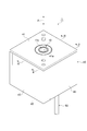
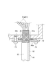
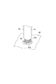
- FIG. 1 is a perspective view of a flash light source device according to an embodiment.
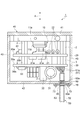
- FIG. 2 is a cross-sectional view of the flash light source device taken along line II-II in FIG.
- FIG. 3 is a cross-sectional view of the flash light source device taken along line III-III in FIG.
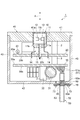
- FIG. 4 is a plan view of the holding and fixing structure of the flash light source device of FIG.
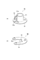
- FIG. 5A is a plan view of a first modification of the holding and fixing structure.
- FIG. 5B is a plan view of a second modification of the holding and fixing structure.
- FIG. 6A is a perspective view of a third modification of the holding and fixing structure.
- FIG. 6B is a perspective view of a fourth modification of the holding and fixing structure.
- FIG. 5A is a plan view of a first modification of the holding and fixing structure.
- FIG. 5B is a plan view of a second modification of the holding and fixing structure.
- FIG. 6A is a perspective view of a
- FIG. 7 is a cross-sectional view of a fifth modification of the holding and fixing structure.
- FIG. 8A is a side view of a sixth modification of the holding and fixing structure.
- FIG. 8B is a side view of a seventh modification of the holding and fixing structure.
- FIG. 9 is a plan view of an eighth modification of the holding and fixing structure.
- FIG. 10 is a perspective view of a ninth modification of the holding and fixing structure.
- the flash light source device 1 includes a flash lamp 10, two wiring boards 20 and 30, and a housing 40.
- the flash lamp 10 includes a sealed container 11, a cathode 12, an anode 13, a trigger electrode (not shown), a sparker electrode (not shown), and a plurality of lead pins 14.
- the flash lamp 10 has a configuration in which a plurality of lead pins 14 protrude from one end of the sealed container 11.
- the flash lamp 10 having such a configuration is different from a straight tube type flash lamp (having a configuration in which the cathode and the anode are arranged apart from each other at both ends of the straight tube), for example, at a high frequency of 10 Hz or more. Suitable for lighting.
- the sealed container 11 includes a side tube 11a, a stem 11b, and a light transmission member 11c.
- the side tube 11a is formed of a metal material, for example, in a cylindrical shape.
- the center line of the side tube 11a is parallel to the direction A.
- the stem 11b is formed of a metal material, for example, in a disk shape.
- the stem 11b closes one end of the side tube 11a.
- the light transmission member 11c is formed of glass, for example, in a disk shape.
- the light transmitting member 11c closes the other end of the side tube 11a.
- a sealing tube 15 is provided on the stem 11b.
- the sealing tube 15 protrudes from one end of the sealed container 11.
- the sealed tube 15 is used for filling the sealed container 11 with a discharge gas, and is sealed after the discharge gas is filled.
- the cathode 12 and the anode 13 are opposed to each other in a direction intersecting the direction A (here, a direction orthogonal to the direction A).
- the cathode 12 and the anode 13 cause arc discharge in the sealed container 11.
- the trigger electrode generates a preliminary discharge prior to the arc discharge.
- the sparker electrode stably generates arc discharge.
- the light generated by the arc discharge is emitted along the direction A through the light transmitting member 11c.
- Each of the cathode 12, the anode 13, the trigger electrode, and the sparker electrode is fixed to the end of each lead pin 14.
- Each lead pin 14 penetrates the stem 11b via an insulating member (not shown), and protrudes from one end of the sealed container 11 as described above.
- the wiring board 20 has a front surface 20a and a back surface 20b facing each other in the direction A.
- the wiring board 20 is disposed in the housing 40 with the front surface 20a facing the first wall 41 side of the housing 40.
- the wiring board 20 is fixed to the first wall portion 41 of the housing 40 via the spacer 2.
- Each lead pin 14 of the flash lamp 10 is fixed to the surface 20a of the wiring board 20 by a conductive bonding member such as solder. Thereby, the flash lamp 10 is electrically connected to a circuit (circuit for causing the flash lamp 10 to emit light) provided on the wiring board 20.
- Circuit components such as a plurality of chip capacitors 21 a and a plurality of resistance elements 22 are mounted on the front surface 20 a and the back surface 20 b of the wiring board 20.
- Each circuit component constitutes a circuit for causing the flash lamp 10 to emit light.
- the plurality of chip capacitors 21 a constitute a power feeding unit 21 that charges and discharges current to be supplied to the flash lamp 10.
- the plurality of chip capacitors 21 a are connected in parallel to each other.
- the wiring board 20 has a through hole 20c.
- the sealing tube 15 of the flash lamp 10 is disposed in the through hole 20c.
- the wiring board 30 has a front surface 30a and a back surface 30b facing each other in the direction A.
- the wiring board 30 is disposed in the housing 40 with the surface 30a facing the wiring board 20 side.
- the wiring board 30 is fixed to the wiring board 20 via the spacer 3.
- Circuit components such as an electrolytic capacitor 31, a transformer (a boost unit) 32, and a resistance element 33 are mounted on the front surface 30 a and the back surface 30 b of the wiring substrate 30.
- Each circuit component constitutes a circuit for causing the flash lamp 10 to emit light.
- the electrolytic capacitor 31 removes power supply noise.
- the transformer 32 is provided between the primary circuit on the power supply side and the secondary circuit on the flash lamp 10 side.
- the transformer 32 amplifies (boosts) a pulse voltage of, for example, 100 to 300 V input to the primary side coil, and outputs a pulse voltage of, for example, 5 to 7 kV from the secondary side coil.
- the housing 40 includes a second wall portion 42 and a plurality of third wall portions 43 in addition to the first wall portion 41 described above.
- the first wall portion 41 and the second wall portion 42 face each other in the direction A via the two wiring boards 20 and 30.
- the plurality of third wall portions 43 are erected on the peripheral edge portion of the second wall portion 42.
- the 2nd wall part 42 and the some 3rd wall part 43 comprise the bottomed container formed integrally.
- the first wall 41 is fixed to the opening by, for example, screwing in a state of being fitted into the opening of the bottomed container.
- a through hole 41 a is formed in the first wall portion 41.
- the sealed container 11 of the flash lamp 10 is disposed in the through hole 41a.
- the outer surface of the light transmission member 11 c of the flash lamp 10 is flush with the outer surface of the first wall portion 41.
- the side tube 11a and the first wall portion 41 of the sealed container 11 are thermally connected by being in contact with each other. Thereby, heat can be efficiently released from the flash lamp 10 that generates heat by light emission to the first wall portion 41 (and thus the first wall portion 41).
- the side tube 11a and the first wall portion 41 of the sealed container 11 may be thermally joined by disposing a heat transfer member therebetween.
- the housing 40 (that is, the first wall portion 41, the second wall portion 42, and the plurality of third wall portions 43) is formed, for example, in a rectangular parallelepiped shape from a conductive material such as a metal material.
- the housing 40 accommodates the flash lamp 10 and the two wiring boards 20 and 30.
- “the housing 40 accommodates the flash lamp 10” means that the housing 40 accommodates at least a portion of each lead pin 14 that protrudes from one end of the sealed container 11.
- the flash light source device 1 further includes an electromagnetic shield cable 50, a holding member 60, and a fixing member 70.
- the electromagnetic shield cable 50 includes a plurality of wirings 51, an electromagnetic shield layer 52, and an insulating protective layer 53.
- the electromagnetic shield cable 50 is a flexible cable for electrically connecting the two wiring boards 20 and 30 and an external circuit.
- the electromagnetic shield cable 50 extends to the inside and the outside of the housing 40 via an opening 45 formed in the second wall portion 42 of the housing 40, for example, in a circular shape.
- the plurality of wirings 51 are exposed inside the housing 40. That is, the electromagnetic shield layer 52 and the insulating protective layer 53 are partially removed at the end portion of the electromagnetic shield cable 50, so that the end portions 51a of the plurality of wirings 51 are exposed to the outside (the space in the housing 40). It has been made.
- Each wiring 51 is directly connected to a predetermined portion of the back surface 30 b of the wiring board 30.
- the end of the conducting wire is exposed by partially removing the insulating protective film, and the conducting wire is exposed to the wiring board 30 by a conductive bonding member such as solder. It is being fixed to the predetermined part of the back surface 30b.
- each wiring 51 is directly connected to the wiring board 30 without connecting components such as connectors.
- Each wiring 51 is, for example, a power supply wiring, a signal input wiring, or the like.
- the electromagnetic shield layer 52 covers the plurality of wires 51 over substantially the entire length of the electromagnetic shield cable 50.
- the electromagnetic shield layer 52 is formed in a tubular shape by a conductive material such as a metal material.
- the electromagnetic shield layer 52 is formed in a tubular shape by a plurality of metal wires knitted in a mesh shape, and the metal wires are electrically connected to each other.
- the insulating protective layer 53 covers the electromagnetic shield layer 52 over substantially the entire length of the electromagnetic shield cable 50.
- the insulating protective layer 53 is formed in a tubular shape by an insulating material such as an elastomer.
- the electromagnetic shield layer 52 is exposed at a portion 52 a corresponding to the opening 45. That is, the insulating protective layer 53 is partially removed in the portion 52a corresponding to the opening 45 in the electromagnetic shield layer 52, so that the portion 52a of the electromagnetic shield layer 52 is exposed to the outside. More specifically, the electromagnetic shield layer 52 includes a portion 40 a that defines the opening 45 in the housing 40 (a region along the edge of the opening 45 of the outer surface of the housing 40, an inner surface of the opening 45, and the housing 40. And a portion including at least one of the regions along the edge of the opening 45 of the inner surface of the inner surface. That is, the insulating protective layer 53 is annularly removed along the portion 40a that defines the opening 45 in the housing 40, so that the portion 52a of the electromagnetic shield layer 52 is exposed to the outside.
- the holding member 60 is formed in a ring shape (C shape) with a part cut away by a conductive material such as a metal material.
- the holding member 60 is provided with a plurality of claw portions 61 protruding inward.
- the holding member 60 is in contact with the portion 52a of the electromagnetic shield layer 52 at the plurality of claw portions 61 by the elastic deformation force, and holds the portion 52a.
- the holding member 60 is in contact with the portion 40 a of the housing 40 on the outside of the housing 40. Thereby, the part 52 a of the electromagnetic shield layer 52 is reliably electrically connected to the part 40 a of the housing 40 through the holding member 60.
- the fixing member 70 is formed in a plate shape from a conductive material such as a metal material.
- An opening 71 and a plurality of through holes 72 are formed in the fixing member 70.
- the electromagnetic shield cable 50 is inserted through the opening 71.
- the plurality of through holes 72 respectively correspond to the plurality of screw holes 42 a formed in the second wall portion 42 of the housing 40.
- a screw 73 made of a conductive material such as a metal material is screwed into each screw hole 42 a via a corresponding through hole 72.
- the fixing member 70 and the screw 73 are indicated by a two-dot chain line, and the wiring 51 is omitted.
- the fixing member 70 is sandwiched between the housing 40 and the housing 40 on the outside of the housing 40, so that the holding member 60 is attached to the portion 40 a of the housing 40. Are securely contacted and fixed.
- the inner diameter of the opening 45 of the housing 40 is larger than the outer diameter of the electromagnetic shield cable 50.
- the inner diameter of the opening 71 of the fixing member 70 is larger than the outer diameter of the electromagnetic shield cable 50 and smaller than the inner diameter of the opening 45 of the housing 40. Therefore, the fixing member 70 is located between the portion 40a of the housing 40 and the portion 52a of the electromagnetic shield layer 52 when viewed from the direction in which the opening 45 opens (direction parallel to the center line of the circular opening 45). It overlaps with the gap so as to cover the gap formed.
- the flash light source device 1 configured as described above will be described.
- power is supplied to the main power supply unit provided on the wiring board 30 via the electromagnetic shield cable 50, whereby the power supply unit 21 is charged, and then a voltage is applied between the cathode 12 and the anode 13. Is done.
- a pulse voltage of 100 to 300 V for example, is applied to the primary coil of the transformer 32.
- the pulse voltage applied to the primary coil is amplified (boosted) by the transformer 32, and a pulse voltage of, for example, 5 to 7 kV is output from the secondary coil.
- the pulse voltage output from the secondary coil is applied to the anode 13 and the sparker electrode.
- preliminary discharge is generated by the sparker electrode, and then preliminary discharge is generated between the cathode 12 or the anode 13 and the trigger electrode, thereby forming a preliminary discharge path.
- main discharge occurs between the cathode 12 and the anode 13 along the preliminary discharge path.
- main discharge arc discharge
- current is supplied through the main power supply unit provided on the wiring substrate 30 and accumulated charge is output from the power supply unit 21.
- the light generated by the arc discharge is emitted along the direction A through the light transmitting member 11c.
- the wiring 51 of the electromagnetic shield cable 50 is directly connected to the wiring board 30.
- the electromagnetic shield cable 50 can be bent from the vicinity of the outside of the opening 45 in the housing 40 as compared with the case where the wiring board 30 and the electromagnetic shield cable 50 are electrically connected via a connector, for example. Therefore, the installation space for the flash light source device 1 can be reduced.
- a portion 52 a corresponding to the opening 45 in the electromagnetic shield layer 52 is electrically connected to a portion 40 a that defines the opening 45 in the housing 40.
- the electromagnetic shield layer 52 is covered with the insulating protective layer 53 in the portion 40a defining the opening 45 in the housing 40, and the electromagnetic shield layer 52 is not electrically connected to the portion 40a.
- the amount of electromagnetic noise emitted from the wiring boards 20 and 30 to the outside of the housing 40 can be reduced.
- the flash light source device 1 it is possible to simultaneously reduce the installation space and suppress the emission of electromagnetic noise.
- a transformer 32 for amplifying (boosting) the pulse voltage is provided on the wiring board 30, and the pulse voltage amplified (boosted) by the transformer 32 is input to each lead pin 14 of the flash lamp 10.
- the flash lamp 10 and the wiring boards 20, 30 are accommodated in the casing 40, and the outer side of the casing 40 is separated from each wiring board 20, 30 by the configuration as described above. It is extremely important to reduce the amount of electromagnetic noise that is emitted to the surface.
- the portion 52 a of the electromagnetic shield layer 52 is held by a holding member 60 made of a conductive material, and the holding member 60 is fixed to the portion 40 a of the housing 40 by the fixing member 70. Yes. Thereby, the electromagnetic shielding layer 52 and the housing
- the fixing member 70 is made of a conductive material. Therefore, with a simple structure, the electromagnetic shielding layer 52 and the housing
- the fixing member 70 overlaps with a gap formed between the portion 40 a of the housing 40 and the portion 52 a of the electromagnetic shield layer 52 when viewed from the direction in which the opening 45 opens. Yes.
- etc. Can be reduced. Therefore, the emission of electromagnetic noise can be more reliably suppressed.
- the reason why the inner diameter of the opening 45 of the housing 40 and the inner diameter of the opening 71 of the fixing member 70 are larger than the outer diameter of the electromagnetic shield cable 50 is to allow the electromagnetic shield cable 50 to be inserted easily.
- the holding member 60 and the fixing member 70 are disposed outside the housing 40. Thereby, the holding member 60 holding the electromagnetic shield layer 52 can be easily fixed to the portion 40 a of the housing 40.
- the electromagnetic shield layer 52 is exposed along the portion 40 a of the housing 40.
- the portion of the electromagnetic shield layer 52 that is disposed inside the housing 40 is covered with the insulating protective layer 53, so that the electromagnetic shield layer 52 contacts a certain member inside the housing 40 and short-circuits. It is possible to prevent such a situation.
- an insulating protective layer that covers a portion of the electromagnetic shield layer 52 that is disposed inside the housing 40. Since 53 contacts the holding member 60, it is possible to suppress a physical load from being applied to the connection portion between the wiring board 30 and each wiring 51.
- the through hole 41 a in which the sealed container 11 of the flash lamp 10 is disposed is formed in the first wall portion 41 of the housing 40, and the opening 45 through which the electromagnetic shield cable 50 is inserted is formed.
- the second wall portion 42 of the housing 40 facing the first wall portion 41 is formed.
- the flash light source device of the present disclosure is not limited to the above-described embodiment.
- a holding member 60 that holds the portion 52a of the electromagnetic shield layer 52 by plastic deformation may be used.
- the holding member 60 shown in FIG. 5A is formed in an annular shape (C-shape) with a part cut away by a conductive material such as a metal material.
- the holding member 60 is deformed so that both end portions of the holding member 60 facing each other in the notched portion overlap each other, so that the portion 52a of the electromagnetic shield layer 52 comes into contact with the holding member 60, and the portion 52 a is held by the holding member 60.
- the holding member 60 shown in FIG. 5B is formed in an annular shape from a conductive material such as a metal material.
- the holding member 60 is deformed so that the portions facing each other through the portion 52 a of the electromagnetic shield layer 52 protrude inwardly so that the portion 52 a of the electromagnetic shield layer 52 contacts the holding member 60. Then, the portion 52 a is held by the holding member 60.
- the holding member 60 can be fixed to the portion 40 a of the housing 40 using the fixing member 70 described above.
- a holding member 80 having both a holding function and a fixing function may be used.
- a holding member 80 shown in FIG. 6A has a circular pipe portion 81, a flange portion 82, and a pair of pedestal portions 83.
- a slit 81 a is formed in the circular pipe portion 81.
- the pair of pedestal portions 83 are provided in the circular tube portion 81 so as to face each other through the slit 81a.
- the flange portion 82 is provided at one end of the circular tube portion 81.
- the flange portion 82 is formed with a slit 82a so as to be continuous with the slit 81a.
- the circular pipe portion 81, the flange portion 82, and the pair of pedestal portions 83 are integrally formed of a conductive material such as a metal material.
- a conductive material such as a metal material.
- the distance between the pair of pedestal portions 83 is reduced by screws, so that the portion 52a of the electromagnetic shield layer 52 becomes the circular tube portion 81.
- the portion 52 a is held by the circular tube portion 81.
- the flange part 82 is fixed to the part 40a of the housing
- a holding member 80 shown in FIG. 6B is a U-shaped member in which a groove 80a into which the electromagnetic shield cable 50 is introduced is formed in a flat plate-like member.
- the U-shaped member has a groove 80a.
- a plurality of claw portions 84 protruding so as to be narrowed are provided.
- the holding member 80 is configured to be fixed to the portion 40a of the housing 40 with a screw. In this case, the portion 52 a of the electromagnetic shield layer 52 comes into contact with each claw portion 84 of the holding member 80, and the portion 52 a is held by the plurality of claw portions 84.
- the part 52 a of the electromagnetic shield layer 52 may be brought into direct contact with the part 40 a of the housing 40.
- the end of the electromagnetic shield layer 52 including the portion 52 a corresponding to the opening 45 is exposed, and the exposed end of the electromagnetic shield layer 52 has a larger diameter than the opening 45.
- a flange portion 52 b is formed in the portion 52 a of the electromagnetic shield layer 52. Then, the flange portion 52 b is fixed to the portion 40 a of the housing 40 by the fixing member 70, so that the portion 52 a of the electromagnetic shield layer 52 is brought into direct contact with the portion 40 a of the housing 40.
- a holding member 80 having both a holding function and a fixing function may be used.
- a holding member 80 shown in FIG. 8A has a pair of annular portions 85 and a plurality of support portions 86.
- the plurality of support portions 86 are spanned between the pair of annular portions 85 so that the space at the center is narrowed.
- the pair of annular portions 85 and the plurality of support portions 86 are integrally formed of a conductive material such as a metal material.
- the plurality of support portions 86 are arranged in the opening 45 of the housing 40, and the portions 52 a of the electromagnetic shield layer 52 are inserted into the holding member 80, so that the space in the center portion is widened.
- the support portion 86 of the first electrode contacts the portion 52a of the electromagnetic shield layer 52 while being deformed. Accordingly, the portion 52a of the electromagnetic shield layer 52 is held by the plurality of support portions 86, and the portion 52a of the electromagnetic shield layer 52 is electrically connected and fixed to the portion 40a of the housing 40.
- the holding member 80 shown in FIG. 8B has a pair of annular portions 85, a plurality of support portions 87, and a plurality of claw portions 88.
- the plurality of support portions 87 are spanned between the pair of annular portions 85.
- the plurality of claw portions 88 extend from one annular portion 85 so that the space at the center is narrowed.
- the pair of annular portions 85, the plurality of support portions 87, and the plurality of claw portions 88 are integrally formed of a conductive material such as a metal material.
- the plurality of support portions 87 are fixed to the openings 45 of the housing 40, and the portions 52a of the electromagnetic shield layer 52 are inserted into the holding member 80, so that the space in the central portion is widened.
- claw part 88 contacts with the part 52a of the electromagnetic shielding layer 52, deform
- the portion 40 a that defines the opening 45 in the housing 40 is composed of a plurality of movable parts having arc-shaped grooves so that the size of the opening 45 is variable. Also good.
- a position where one portion constituting the portion 40a of the housing 40 is shifted from the other portion in the direction perpendicular to the plane of the paper in FIG. With this relationship, the size (width) of the opening 45 can be narrowed, and the portion 52a of the electromagnetic shield layer 52 can be sandwiched. Thereby, the part 52a of the electromagnetic shielding layer 52 is electrically connected and fixed to the part 40a of the housing 40. Further, as shown in FIG.
- the portion 52 a of the electromagnetic shield layer 52 is in contact with the portion 40 a of the housing 40 by a conductive bonding member 90 such as solder, and the portion 52 a is electrically conductive with the portion 40 a of the housing 40. It may be fixed by the joining member 90. Alternatively, the portion 52a of the electromagnetic shield layer 52 may be directly joined to the portion 40a of the housing 40 by welding.
- the wiring board provided with a circuit for causing the flash lamp 10 to emit light is not limited to the two wiring boards 20 and 30, and may be one wiring board, or three or more wirings. It may be a substrate.
- the opening 45 may be formed in a wall portion other than the second wall portion 42 in the housing 40.
- the electromagnetic shield layer 52 only needs to be exposed at least in a portion corresponding to the opening 45 of the housing 40.
- the end portion of the electromagnetic shield layer 52 including the portion 52 a corresponding to the opening 45 may be exposed.
- the number of wirings 51 is not limited.
- the holding member 60 and the fixing member 70 may be disposed inside the housing 40. If at least the holding member 60 is made of a conductive material, the fixing member 70 may not be made of a conductive material.
- the side tube 11a of the sealed container 11 of the flash lamp 10 may be formed in another shape (for example, a substantially polygonal cylindrical shape) with another material (for example, glass or the like).
- the flash lamp 10 is a head-on type that extracts light in a direction along the direction A, but may be a side-on type that extracts light in a direction intersecting the direction A.
- the cathode 12 and the anode 13 are arranged side by side in the direction intersecting the direction A, they may be arranged side by side in the direction along the direction A.
- the plurality of lead pins 14 of the flash lamp 10 are directly fixed to the wiring board 20 by a conductive bonding member such as solder, but are fixed to the wiring board 20 through sockets into which the lead pins 14 are fitted. Also good.
- SYMBOLS 1 Flash light source device, 10 ... Flash lamp, 11 ... Sealed container, 20, 30 ... Wiring board, 40 ... Housing
Abstract
A flash light source device of the present invention is equipped with: a flash lamp; a wiring board that is provided with a circuit for making the flash lamp emit light; a housing, which is formed of a conductive material, and which houses the flash lamp and the wiring board; and an electromagnetic shield cable, which has wiring directly connected to the wiring board, an electromagnetic shield layer covering the wiring, and an insulating protection layer covering the electromagnetic shield layer, and which extends to the inner side and the outer side of the housing through an opening formed in the housing. At least an electromagnetic shield layer portion corresponding to the opening is exposed. The electromagnetic shield layer portion corresponding to the opening is electrically connected to a housing portion defining the opening.
Description
本開示は、フラッシュ光源装置に関する。
The present disclosure relates to a flash light source device.
特許文献1記載のフラッシュ光源装置は、フラッシュランプと、フラッシュランプを発光させるための回路が設けられた配線基板と、フラッシュランプ及び配線基板を収容する筐体と、を備えている。
The flash light source device described in Patent Document 1 includes a flash lamp, a wiring board on which a circuit for causing the flash lamp to emit light is provided, and a housing that houses the flash lamp and the wiring board.
特許文献1記載のフラッシュ光源装置は十分な小型化が可能であるが、更なる設置スペースの縮小化及び電磁ノイズの放出の抑制が求められている。
Although the flash light source device described in Patent Document 1 can be sufficiently reduced in size, it is required to further reduce the installation space and suppress the emission of electromagnetic noise.
本開示は、設置スペースの縮小化及び電磁ノイズの放出の抑制を両立し得るフラッシュ光源装置を提供することを目的とする。
This disclosure is intended to provide a flash light source device capable of both reducing the installation space and suppressing the emission of electromagnetic noise.
本開示の一形態に係るフラッシュ光源装置は、フラッシュランプと、フラッシュランプを発光させるための回路が設けられた配線基板と、導電性材料からなり、フラッシュランプ及び配線基板を収容する筐体と、配線基板に直接的に接続された配線、配線を覆う電磁シールド層、及び電磁シールド層を覆う絶縁性保護層を有し、筐体に形成された開口を介して筐体の内側及び外側に延在する電磁シールドケーブルと、を備え、電磁シールド層は、少なくとも開口に対応する部分において露出させられており、電磁シールド層のうち開口に対応する部分は、筐体のうち開口を画定する部分に電気的に接続されている。
A flash light source device according to an embodiment of the present disclosure includes a flash lamp, a wiring board provided with a circuit for causing the flash lamp to emit light, a housing made of a conductive material and containing the flash lamp and the wiring board, It has wiring directly connected to the wiring board, an electromagnetic shield layer that covers the wiring, and an insulating protective layer that covers the electromagnetic shield layer, and extends to the inside and outside of the housing through openings formed in the housing. An electromagnetic shield cable, and the electromagnetic shield layer is exposed at least in a portion corresponding to the opening, and the portion corresponding to the opening of the electromagnetic shield layer is a portion of the housing that defines the opening. Electrically connected.
このフラッシュ光源装置では、電磁シールドケーブルの配線が配線基板に直接的に接続されている。そのため、例えばコネクタを介して配線基板と電磁シールドケーブルとを電気的に接続するような場合に比べ、筐体における開口の外側近傍から電磁シールドケーブルを撓ませることができる。したがって、フラッシュ光源装置の設置スペースを縮小化することができる。また、電磁シールド層のうち開口に対応する部分が、筐体のうち開口を画定する部分に電気的に接続されている。これにより、筐体のうち開口を画定する部分において電磁シールド層が絶縁性保護層に覆われており当該部分に電磁シールド層が電気的に接続されていない場合に比べ、配線基板等から筐体の外側に放出される電磁ノイズの量を減少させることができる。以上により、このフラッシュ光源装置によれば、設置スペースの縮小化及び電磁ノイズの放出の抑制を両立することができる。
In this flash light source device, the wiring of the electromagnetic shield cable is directly connected to the wiring board. Therefore, compared with the case where a wiring board and an electromagnetic shielding cable are electrically connected through a connector, for example, an electromagnetic shielding cable can be bent from the outside vicinity of the opening in a housing | casing. Therefore, the installation space for the flash light source device can be reduced. In addition, a portion of the electromagnetic shield layer corresponding to the opening is electrically connected to a portion of the housing that defines the opening. As a result, the electromagnetic shield layer is covered with the insulating protective layer in the portion of the case that defines the opening, and the case from the wiring board or the like compared to the case where the electromagnetic shield layer is not electrically connected to the portion. It is possible to reduce the amount of electromagnetic noise emitted outside. As described above, according to this flash light source device, it is possible to achieve both reduction in installation space and suppression of emission of electromagnetic noise.
本開示の一形態に係るフラッシュ光源装置は、導電性材料からなり、電磁シールド層のうち開口に対応する部分を保持する保持部材と、筐体のうち開口を画定する部分に保持部材を固定する固定部材と、を更に備えてもよい。これによれば、簡易な構成で、電磁シールド層と筐体とを確実に電気的に接続することができる。
A flash light source device according to an embodiment of the present disclosure includes a holding member that holds a portion corresponding to an opening in an electromagnetic shield layer and a holding member that is fixed to a portion of the housing that defines the opening. And a fixing member. According to this, the electromagnetic shield layer and the housing can be reliably electrically connected with a simple configuration.
本開示の一形態に係るフラッシュ光源装置では、固定部材は、導電性材料からなってもよい。これによれば、簡易な構成で、電磁シールド層と筐体とをより確実に電気的に接続することができる。
In the flash light source device according to an embodiment of the present disclosure, the fixing member may be made of a conductive material. According to this, the electromagnetic shield layer and the housing can be more reliably electrically connected with a simple configuration.
本開示の一形態に係るフラッシュ光源装置では、固定部材は、開口が開口する方向から見た場合に、筐体のうち開口を画定する部分と電磁シールド層のうち開口に対応する部分との間に形成される隙間と重なっていてもよい。これによれば、配線基板等から当該隙間を介して筐体の外側に放出される電磁ノイズの量を減少させることができる。したがって、電磁ノイズの放出をより確実に抑制することができる。
In the flash light source device according to an aspect of the present disclosure, the fixing member is between the portion of the housing that defines the opening and the portion of the electromagnetic shield layer that corresponds to the opening when viewed from the direction in which the opening opens. It may overlap with the gap formed. According to this, the amount of electromagnetic noise emitted from the wiring board or the like to the outside of the housing through the gap can be reduced. Therefore, the emission of electromagnetic noise can be more reliably suppressed.
本開示の一形態に係るフラッシュ光源装置では、保持部材及び固定部材は、筐体の外側に配置されていてもよい。これによれば、筐体のうち開口を画定する部分に、電磁シールド層を保持した保持部材を容易に固定することができる。
In the flash light source device according to an aspect of the present disclosure, the holding member and the fixing member may be disposed outside the housing. According to this, the holding member holding the electromagnetic shield layer can be easily fixed to the portion of the housing that defines the opening.
本開示の一形態に係るフラッシュ光源装置では、電磁シールド層は、筐体のうち開口を画定する部分に沿って露出させられていてもよい。これによれば、電磁シールド層のうち筐体の内側に配置される部分が絶縁性保護層に覆われているので、筐体の内側において電磁シールド層が何らかの部材に接触してショートするような事態を防止することができる。
In the flash light source device according to an aspect of the present disclosure, the electromagnetic shield layer may be exposed along a portion of the housing that defines the opening. According to this, since the portion of the electromagnetic shield layer disposed inside the housing is covered with the insulating protective layer, the electromagnetic shield layer is in contact with any member and shorts inside the housing. The situation can be prevented.
本開示の一形態に係るフラッシュ光源装置では、筐体には、フラッシュランプの密封容器が配置された貫通孔が形成されており、貫通孔は、筐体の第1壁部に形成されており、開口は、第1壁部と対向する筐体の第2壁部に形成されていてもよい。これによれば、特に第1壁部と第2壁部とが対向する方向に垂直な方向において、フラッシュ光源装置の設置スペースを縮小化することができる。
In the flash light source device according to an aspect of the present disclosure, the housing has a through hole in which a sealed container of the flash lamp is disposed, and the through hole is formed in the first wall portion of the housing. The opening may be formed in the second wall portion of the housing facing the first wall portion. According to this, the installation space of the flash light source device can be reduced particularly in the direction perpendicular to the direction in which the first wall portion and the second wall portion face each other.
本開示によれば、設置スペースの縮小化及び電磁ノイズの放出の抑制を両立し得るフラッシュ光源装置を提供することが可能となる。
According to the present disclosure, it is possible to provide a flash light source device that can simultaneously reduce the installation space and suppress the emission of electromagnetic noise.
以下、本開示の実施形態について、図面を参照して詳細に説明する。なお、各図において同一又は相当部分には同一符号を付し、重複する説明を省略する。
Hereinafter, embodiments of the present disclosure will be described in detail with reference to the drawings. In addition, in each figure, the same code | symbol is attached | subjected to the same or an equivalent part, and the overlapping description is abbreviate | omitted.
図1、図2及び図3に示されるように、フラッシュ光源装置1は、フラッシュランプ10と、2枚の配線基板20,30と、筐体40と、を備えている。フラッシュランプ10は、密封容器11と、陰極12と、陽極13と、トリガ電極(図示省略)と、スパーカ電極(図示省略)と、複数のリードピン14と、を有している。フラッシュランプ10は、複数のリードピン14が密封容器11の一端部から突出した構成を有している。このような構成を有するフラッシュランプ10は、直管型のフラッシュランプ(陰極及び陽極が直管の両端部に互いに離れて配置された構成を有するもの)とは異なり、例えば10Hz以上といった高周波数での点灯に適している。
As shown in FIGS. 1, 2, and 3, the flash light source device 1 includes a flash lamp 10, two wiring boards 20 and 30, and a housing 40. The flash lamp 10 includes a sealed container 11, a cathode 12, an anode 13, a trigger electrode (not shown), a sparker electrode (not shown), and a plurality of lead pins 14. The flash lamp 10 has a configuration in which a plurality of lead pins 14 protrude from one end of the sealed container 11. The flash lamp 10 having such a configuration is different from a straight tube type flash lamp (having a configuration in which the cathode and the anode are arranged apart from each other at both ends of the straight tube), for example, at a high frequency of 10 Hz or more. Suitable for lighting.
密封容器11内には、放電ガス(例えばキセノンガス)が封入されている。密封容器11は、側管11a、ステム11b及び光透過部材11cによって構成されている。側管11aは、金属材料によって、例えば円筒状に形成されている。側管11aの中心線は、方向Aに平行である。ステム11bは、金属材料によって、例えば円板状に形成されている。ステム11bは、側管11aの一端部を塞いでいる。光透過部材11cは、ガラスによって、例えば円板状に形成されている。光透過部材11cは、側管11aの他端部を塞いでいる。なお、ステム11bには、封止管15が設けられている。封止管15は、密封容器11の一端部から突出している。封止管15は、密封容器11内に放電ガスを充填するために用いられ、放電ガスの充填後に封止されたものである。
In the sealed container 11, a discharge gas (for example, xenon gas) is sealed. The sealed container 11 includes a side tube 11a, a stem 11b, and a light transmission member 11c. The side tube 11a is formed of a metal material, for example, in a cylindrical shape. The center line of the side tube 11a is parallel to the direction A. The stem 11b is formed of a metal material, for example, in a disk shape. The stem 11b closes one end of the side tube 11a. The light transmission member 11c is formed of glass, for example, in a disk shape. The light transmitting member 11c closes the other end of the side tube 11a. Note that a sealing tube 15 is provided on the stem 11b. The sealing tube 15 protrudes from one end of the sealed container 11. The sealed tube 15 is used for filling the sealed container 11 with a discharge gas, and is sealed after the discharge gas is filled.
陰極12及び陽極13は、方向Aと交差する方向(ここでは、方向Aと直交する方向)において互いに対向している。陰極12及び陽極13は、密封容器11内においてアーク放電を生じさせる。トリガ電極は、アーク放電に先立って予備放電を生じさせる。スパーカ電極は、アーク放電を安定して生じさせる。アーク放電によって発生した光は、光透過部材11cを介して方向Aに沿って出射される。陰極12、陽極13、トリガ電極及びスパーカ電極のそれぞれは、各リードピン14の端部に固定されている。各リードピン14は、絶縁部材(図示省略)を介してステム11bを貫通しており、上述したように、密封容器11の一端部から突出している。
The cathode 12 and the anode 13 are opposed to each other in a direction intersecting the direction A (here, a direction orthogonal to the direction A). The cathode 12 and the anode 13 cause arc discharge in the sealed container 11. The trigger electrode generates a preliminary discharge prior to the arc discharge. The sparker electrode stably generates arc discharge. The light generated by the arc discharge is emitted along the direction A through the light transmitting member 11c. Each of the cathode 12, the anode 13, the trigger electrode, and the sparker electrode is fixed to the end of each lead pin 14. Each lead pin 14 penetrates the stem 11b via an insulating member (not shown), and protrudes from one end of the sealed container 11 as described above.
配線基板20は、方向Aにおいて互いに対向する表面20a及び裏面20bを有している。配線基板20は、表面20aが筐体40の第1壁部41側に向いた状態で、筐体40内に配置されている。配線基板20は、スペーサ2を介して筐体40の第1壁部41に固定されている。配線基板20の表面20aには、フラッシュランプ10の各リードピン14が半田等の導電性接合部材によって固定されている。これにより、フラッシュランプ10は、配線基板20に設けられた回路(フラッシュランプ10を発光させるための回路)に電気的に接続されている。
The wiring board 20 has a front surface 20a and a back surface 20b facing each other in the direction A. The wiring board 20 is disposed in the housing 40 with the front surface 20a facing the first wall 41 side of the housing 40. The wiring board 20 is fixed to the first wall portion 41 of the housing 40 via the spacer 2. Each lead pin 14 of the flash lamp 10 is fixed to the surface 20a of the wiring board 20 by a conductive bonding member such as solder. Thereby, the flash lamp 10 is electrically connected to a circuit (circuit for causing the flash lamp 10 to emit light) provided on the wiring board 20.
配線基板20の表面20a及び裏面20bには、複数のチップコンデンサ21a、複数の抵抗素子22等の回路部品が実装されている。各回路部品は、フラッシュランプ10を発光させるための回路を構成している。一例として、複数のチップコンデンサ21aは、フラッシュランプ10に供給するための電流の充電及び放電を行う給電部21を構成している。給電部21において、複数のチップコンデンサ21aは、互いに並列に接続されている。なお、配線基板20には、貫通孔20cが形成されている。貫通孔20cには、フラッシュランプ10の封止管15が配置されている。
Circuit components such as a plurality of chip capacitors 21 a and a plurality of resistance elements 22 are mounted on the front surface 20 a and the back surface 20 b of the wiring board 20. Each circuit component constitutes a circuit for causing the flash lamp 10 to emit light. As an example, the plurality of chip capacitors 21 a constitute a power feeding unit 21 that charges and discharges current to be supplied to the flash lamp 10. In the power feeding unit 21, the plurality of chip capacitors 21 a are connected in parallel to each other. The wiring board 20 has a through hole 20c. The sealing tube 15 of the flash lamp 10 is disposed in the through hole 20c.
配線基板30は、方向Aにおいて互いに対向する表面30a及び裏面30bを有している。配線基板30は、表面30aが配線基板20側に向いた状態で、筐体40内に配置されている。配線基板30は、スペーサ3を介して配線基板20に固定されている。配線基板30の表面30a及び裏面30bには、電解コンデンサ31、トランス(昇圧部)32、抵抗素子33等の回路部品が実装されている。各回路部品は、フラッシュランプ10を発光させるための回路を構成している。一例として、電解コンデンサ31は、電源ノイズを除去する。トランス32は、電源側の一次回路とフラッシュランプ10側の二次回路との間に設けられている。トランス32は、一次側コイルに入力された例えば100~300Vのパルス電圧を増幅(昇圧)し、例えば5~7kVのパルス電圧を二次側コイルから出力する。
The wiring board 30 has a front surface 30a and a back surface 30b facing each other in the direction A. The wiring board 30 is disposed in the housing 40 with the surface 30a facing the wiring board 20 side. The wiring board 30 is fixed to the wiring board 20 via the spacer 3. Circuit components such as an electrolytic capacitor 31, a transformer (a boost unit) 32, and a resistance element 33 are mounted on the front surface 30 a and the back surface 30 b of the wiring substrate 30. Each circuit component constitutes a circuit for causing the flash lamp 10 to emit light. As an example, the electrolytic capacitor 31 removes power supply noise. The transformer 32 is provided between the primary circuit on the power supply side and the secondary circuit on the flash lamp 10 side. The transformer 32 amplifies (boosts) a pulse voltage of, for example, 100 to 300 V input to the primary side coil, and outputs a pulse voltage of, for example, 5 to 7 kV from the secondary side coil.
筐体40は、上述した第1壁部41に加え、第2壁部42及び複数の第3壁部43を有している。第1壁部41及び第2壁部42は、2枚の配線基板20,30を介して、方向Aにおいて互いに対向している。複数の第3壁部43は、第2壁部42の周縁部に立設されている。第2壁部42及び複数の第3壁部43は、一体的に形成された有底容器を構成している。第1壁部41は、当該有底容器の開口部に嵌められた状態で、例えばネジ止めによって当該開口部に固定されている。
The housing 40 includes a second wall portion 42 and a plurality of third wall portions 43 in addition to the first wall portion 41 described above. The first wall portion 41 and the second wall portion 42 face each other in the direction A via the two wiring boards 20 and 30. The plurality of third wall portions 43 are erected on the peripheral edge portion of the second wall portion 42. The 2nd wall part 42 and the some 3rd wall part 43 comprise the bottomed container formed integrally. The first wall 41 is fixed to the opening by, for example, screwing in a state of being fitted into the opening of the bottomed container.
第1壁部41には、貫通孔41aが形成されている。貫通孔41aには、フラッシュランプ10の密封容器11が配置されている。フラッシュランプ10の光透過部材11cの外面は、第1壁部41の外面と面一になっている。密封容器11の側管11aと第1壁部41とは、互いに接触することで、熱的に接続されている。これにより、発光によって発熱したフラッシュランプ10から第1壁部41(延いては、第1壁部41)に効率良く熱を逃がすことができる。なお、密封容器11の側管11aと第1壁部41とは、それらの間に伝熱部材が配置されることで、熱的に接合されていてもよい。
A through hole 41 a is formed in the first wall portion 41. The sealed container 11 of the flash lamp 10 is disposed in the through hole 41a. The outer surface of the light transmission member 11 c of the flash lamp 10 is flush with the outer surface of the first wall portion 41. The side tube 11a and the first wall portion 41 of the sealed container 11 are thermally connected by being in contact with each other. Thereby, heat can be efficiently released from the flash lamp 10 that generates heat by light emission to the first wall portion 41 (and thus the first wall portion 41). In addition, the side tube 11a and the first wall portion 41 of the sealed container 11 may be thermally joined by disposing a heat transfer member therebetween.
筐体40(すなわち、第1壁部41、第2壁部42及び複数の第3壁部43)は、金属材料等の導電性材料によって、例えば直方体状に形成されている。筐体40は、フラッシュランプ10及び2枚の配線基板20,30を収容している。ここで、「筐体40がフラッシュランプ10を収容する」とは、少なくとも各リードピン14のうち密封容器11の一端部から突出した部分を筐体40が収容することを意味する。
The housing 40 (that is, the first wall portion 41, the second wall portion 42, and the plurality of third wall portions 43) is formed, for example, in a rectangular parallelepiped shape from a conductive material such as a metal material. The housing 40 accommodates the flash lamp 10 and the two wiring boards 20 and 30. Here, “the housing 40 accommodates the flash lamp 10” means that the housing 40 accommodates at least a portion of each lead pin 14 that protrudes from one end of the sealed container 11.
更に、フラッシュ光源装置1は、電磁シールドケーブル50と、保持部材60と、固定部材70と、を備えている。電磁シールドケーブル50は、複数の配線51と、電磁シールド層52と、絶縁性保護層53と、を有している。電磁シールドケーブル50は、2枚の配線基板20,30と外部の回路とを電気的に接続するための可撓性のケーブルである。電磁シールドケーブル50は、筐体40の第2壁部42に例えば円形状に形成された開口45を介して筐体40の内側及び外側に延在している。
The flash light source device 1 further includes an electromagnetic shield cable 50, a holding member 60, and a fixing member 70. The electromagnetic shield cable 50 includes a plurality of wirings 51, an electromagnetic shield layer 52, and an insulating protective layer 53. The electromagnetic shield cable 50 is a flexible cable for electrically connecting the two wiring boards 20 and 30 and an external circuit. The electromagnetic shield cable 50 extends to the inside and the outside of the housing 40 via an opening 45 formed in the second wall portion 42 of the housing 40, for example, in a circular shape.
複数の配線51は、筐体40の内側において露出させられている。つまり、電磁シールドケーブル50の端部において電磁シールド層52及び絶縁性保護層53が部分的に除去されることで、複数の配線51の端部51aが外部(筐体40内の空間)に露出させられている。各配線51は、配線基板30の裏面30bの所定部に直接的に接続されている。一例として、各配線51の端部51aでは、絶縁性保護膜が部分的に除去されることで導線の端部が露出させられており、当該導線が半田等の導電性接合部材によって配線基板30の裏面30bの所定部に固定されている。このように、各配線51は、コネクタ等の接続部品を介することなく、配線基板30に直接的に接続されている。なお、各配線51は、例えば、電力供給配線、信号入力配線等である。
The plurality of wirings 51 are exposed inside the housing 40. That is, the electromagnetic shield layer 52 and the insulating protective layer 53 are partially removed at the end portion of the electromagnetic shield cable 50, so that the end portions 51a of the plurality of wirings 51 are exposed to the outside (the space in the housing 40). It has been made. Each wiring 51 is directly connected to a predetermined portion of the back surface 30 b of the wiring board 30. As an example, at the end 51a of each wiring 51, the end of the conducting wire is exposed by partially removing the insulating protective film, and the conducting wire is exposed to the wiring board 30 by a conductive bonding member such as solder. It is being fixed to the predetermined part of the back surface 30b. Thus, each wiring 51 is directly connected to the wiring board 30 without connecting components such as connectors. Each wiring 51 is, for example, a power supply wiring, a signal input wiring, or the like.
電磁シールド層52は、電磁シールドケーブル50の略全長に渡って、複数の配線51を覆っている。電磁シールド層52は、金属材料等の導電性材料によって管状に形成されている。一例として、電磁シールド層52は、網目状に編まれた複数の金属線によって管状に形成されており、金属線同士は、互いに電気的に接続されている。絶縁性保護層53は、電磁シールドケーブル50の略全長に渡って、電磁シールド層52を覆っている。絶縁性保護層53は、例えばエラストマー等の絶縁性材料によって管状に形成されている。
The electromagnetic shield layer 52 covers the plurality of wires 51 over substantially the entire length of the electromagnetic shield cable 50. The electromagnetic shield layer 52 is formed in a tubular shape by a conductive material such as a metal material. As an example, the electromagnetic shield layer 52 is formed in a tubular shape by a plurality of metal wires knitted in a mesh shape, and the metal wires are electrically connected to each other. The insulating protective layer 53 covers the electromagnetic shield layer 52 over substantially the entire length of the electromagnetic shield cable 50. The insulating protective layer 53 is formed in a tubular shape by an insulating material such as an elastomer.
電磁シールド層52は、開口45に対応する部分52aにおいて露出させられている。つまり、電磁シールド層52のうち開口45に対応する部分52aにおいて絶縁性保護層53が部分的に除去されることで、電磁シールド層52の部分52aが外部に露出させられている。より具体的には、電磁シールド層52は、筐体40のうち開口45を画定する部分40a(筐体40の外面のうち開口45の縁に沿った領域、開口45の内面、及び筐体40の内面のうち開口45の縁に沿った領域の少なくとも1つを含む部分)に沿って露出させられている。つまり、筐体40のうち開口45を画定する部分40aに沿って絶縁性保護層53が環状に除去されることで、電磁シールド層52の部分52aが外部に露出させられている。
The electromagnetic shield layer 52 is exposed at a portion 52 a corresponding to the opening 45. That is, the insulating protective layer 53 is partially removed in the portion 52a corresponding to the opening 45 in the electromagnetic shield layer 52, so that the portion 52a of the electromagnetic shield layer 52 is exposed to the outside. More specifically, the electromagnetic shield layer 52 includes a portion 40 a that defines the opening 45 in the housing 40 (a region along the edge of the opening 45 of the outer surface of the housing 40, an inner surface of the opening 45, and the housing 40. And a portion including at least one of the regions along the edge of the opening 45 of the inner surface of the inner surface. That is, the insulating protective layer 53 is annularly removed along the portion 40a that defines the opening 45 in the housing 40, so that the portion 52a of the electromagnetic shield layer 52 is exposed to the outside.
図4に示されるように、保持部材60は、金属材料等の導電性材料によって、一部が切り欠かれた環状(C字状)に形成されている。保持部材60には、内側に突出した複数の爪部61が設けられている。保持部材60は、弾性変形力によって、複数の爪部61において電磁シールド層52の部分52aと接触し、当該部分52aを保持している。図2及び図3に示されるように、保持部材60は、筐体40の外側において筐体40の部分40aに接触している。これにより、電磁シールド層52の部分52aは、保持部材60を介して、筐体40の部分40aに確実に電気的に接続される。
As shown in FIG. 4, the holding member 60 is formed in a ring shape (C shape) with a part cut away by a conductive material such as a metal material. The holding member 60 is provided with a plurality of claw portions 61 protruding inward. The holding member 60 is in contact with the portion 52a of the electromagnetic shield layer 52 at the plurality of claw portions 61 by the elastic deformation force, and holds the portion 52a. As shown in FIGS. 2 and 3, the holding member 60 is in contact with the portion 40 a of the housing 40 on the outside of the housing 40. Thereby, the part 52 a of the electromagnetic shield layer 52 is reliably electrically connected to the part 40 a of the housing 40 through the holding member 60.
図4に示されるように、固定部材70は、金属材料等の導電性材料によって板状に形成されている。固定部材70には、開口71及び複数の貫通孔72が形成されている。開口71には、電磁シールドケーブル50が挿通されている。複数の貫通孔72は、筐体40の第2壁部42に形成された複数のネジ穴42aにそれぞれ対応している。各ネジ穴42aには、対応する貫通孔72を介して、金属材料等の導電性材料からなるネジ73が螺合されている。なお、図4では、固定部材70及びネジ73が二点鎖線で示されており、配線51が省略されている。図2及び図3に示されるように、固定部材70は、筐体40の外側において筐体40との間に保持部材60を覆うように挟むことで、筐体40の部分40aに保持部材60を確実に接触させ且つ固定している。
As shown in FIG. 4, the fixing member 70 is formed in a plate shape from a conductive material such as a metal material. An opening 71 and a plurality of through holes 72 are formed in the fixing member 70. The electromagnetic shield cable 50 is inserted through the opening 71. The plurality of through holes 72 respectively correspond to the plurality of screw holes 42 a formed in the second wall portion 42 of the housing 40. A screw 73 made of a conductive material such as a metal material is screwed into each screw hole 42 a via a corresponding through hole 72. In FIG. 4, the fixing member 70 and the screw 73 are indicated by a two-dot chain line, and the wiring 51 is omitted. As illustrated in FIGS. 2 and 3, the fixing member 70 is sandwiched between the housing 40 and the housing 40 on the outside of the housing 40, so that the holding member 60 is attached to the portion 40 a of the housing 40. Are securely contacted and fixed.
図4に示されるように、筐体40の開口45の内径は、電磁シールドケーブル50の外径よりも大きい。固定部材70の開口71の内径は、電磁シールドケーブル50の外径よりも大きく且つ筐体40の開口45の内径よりも小さい。したがって、固定部材70は、開口45が開口する方向(円形状の開口45の中心線に平行な方向)から見た場合に、筐体40の部分40aと電磁シールド層52の部分52aとの間に形成される隙間を覆うように当該隙間と重なっている。
As shown in FIG. 4, the inner diameter of the opening 45 of the housing 40 is larger than the outer diameter of the electromagnetic shield cable 50. The inner diameter of the opening 71 of the fixing member 70 is larger than the outer diameter of the electromagnetic shield cable 50 and smaller than the inner diameter of the opening 45 of the housing 40. Therefore, the fixing member 70 is located between the portion 40a of the housing 40 and the portion 52a of the electromagnetic shield layer 52 when viewed from the direction in which the opening 45 opens (direction parallel to the center line of the circular opening 45). It overlaps with the gap so as to cover the gap formed.
以上のように構成されたフラッシュ光源装置1の動作について説明する。まず、電磁シールドケーブル50を介して配線基板30に設けられた主電源部に電力が供給されることで、給電部21が充電され、その後に、陰極12と陽極13との間に電圧が印加される。その一方で、トランス32の一次側コイルに例えば100~300Vのパルス電圧が印加される。一次側コイルに印加されたパルス電圧は、トランス32において増幅(昇圧)され、例えば5~7kVのパルス電圧が二次側コイルから出力される。二次側コイルから出力されたパルス電圧は、陽極13及びスパーカ電極に印加される。
The operation of the flash light source device 1 configured as described above will be described. First, power is supplied to the main power supply unit provided on the wiring board 30 via the electromagnetic shield cable 50, whereby the power supply unit 21 is charged, and then a voltage is applied between the cathode 12 and the anode 13. Is done. On the other hand, a pulse voltage of 100 to 300 V, for example, is applied to the primary coil of the transformer 32. The pulse voltage applied to the primary coil is amplified (boosted) by the transformer 32, and a pulse voltage of, for example, 5 to 7 kV is output from the secondary coil. The pulse voltage output from the secondary coil is applied to the anode 13 and the sparker electrode.
フラッシュランプ10では、まず、スパーカ電極により予備放電が生じ、続いて、陰極12又は陽極13とトリガ電極との間において予備放電が生じ、これらにより、予備放電路が形成される。その後直ちに、陰極12と陽極13との間において、予備放電路に沿って主放電が生じる。陰極12と陽極13との間において主放電(アーク放電)が生じると、配線基板30に設けられた主電源部を介して電流が供給されると共に給電部21から蓄積電荷が出力される。アーク放電によって発生した光は、光透過部材11cを介して方向Aに沿って出射される。
In the flash lamp 10, first, preliminary discharge is generated by the sparker electrode, and then preliminary discharge is generated between the cathode 12 or the anode 13 and the trigger electrode, thereby forming a preliminary discharge path. Immediately thereafter, main discharge occurs between the cathode 12 and the anode 13 along the preliminary discharge path. When main discharge (arc discharge) occurs between the cathode 12 and the anode 13, current is supplied through the main power supply unit provided on the wiring substrate 30 and accumulated charge is output from the power supply unit 21. The light generated by the arc discharge is emitted along the direction A through the light transmitting member 11c.
以上説明したように、フラッシュ光源装置1では、電磁シールドケーブル50の配線51が配線基板30に直接的に接続されている。そのため、例えばコネクタを介して配線基板30と電磁シールドケーブル50とを電気的に接続するような場合に比べ、筐体40における開口45の外側近傍から電磁シールドケーブル50を撓ませることができる。したがって、フラッシュ光源装置1の設置スペースを縮小化することができる。また、電磁シールド層52のうち開口45に対応する部分52aが、筐体40のうち開口45を画定する部分40aに電気的に接続されている。これにより、筐体40のうち開口45を画定する部分40aにおいて電磁シールド層52が絶縁性保護層53に覆われており当該部分40aに電磁シールド層52が電気的に接続されていない場合に比べ、各配線基板20,30等から筐体40の外側に放出される電磁ノイズの量を減少させることができる。以上により、フラッシュ光源装置1によれば、設置スペースの縮小化及び電磁ノイズの放出の抑制を両立することができる。
As described above, in the flash light source device 1, the wiring 51 of the electromagnetic shield cable 50 is directly connected to the wiring board 30. For this reason, the electromagnetic shield cable 50 can be bent from the vicinity of the outside of the opening 45 in the housing 40 as compared with the case where the wiring board 30 and the electromagnetic shield cable 50 are electrically connected via a connector, for example. Therefore, the installation space for the flash light source device 1 can be reduced. In addition, a portion 52 a corresponding to the opening 45 in the electromagnetic shield layer 52 is electrically connected to a portion 40 a that defines the opening 45 in the housing 40. As a result, the electromagnetic shield layer 52 is covered with the insulating protective layer 53 in the portion 40a defining the opening 45 in the housing 40, and the electromagnetic shield layer 52 is not electrically connected to the portion 40a. The amount of electromagnetic noise emitted from the wiring boards 20 and 30 to the outside of the housing 40 can be reduced. As described above, according to the flash light source device 1, it is possible to simultaneously reduce the installation space and suppress the emission of electromagnetic noise.
なお、フラッシュ光源装置1では、パルス電圧を増幅(昇圧)するトランス32が配線基板30に設けられており、トランス32によって増幅(昇圧)されたパルス電圧がフラッシュランプ10の各リードピン14に入力される。そのため、特に、フラッシュ光源装置1では、筐体40にフラッシュランプ10及び配線基板20,30を収容させること、並びに、上述したような構成によって、各配線基板20,30等から筐体40の外側に放出される電磁ノイズの量を減少させることは、極めて重要である。
In the flash light source device 1, a transformer 32 for amplifying (boosting) the pulse voltage is provided on the wiring board 30, and the pulse voltage amplified (boosted) by the transformer 32 is input to each lead pin 14 of the flash lamp 10. The Therefore, in particular, in the flash light source device 1, the flash lamp 10 and the wiring boards 20, 30 are accommodated in the casing 40, and the outer side of the casing 40 is separated from each wiring board 20, 30 by the configuration as described above. It is extremely important to reduce the amount of electromagnetic noise that is emitted to the surface.
また、フラッシュ光源装置1は、電磁シールド層52の部分52aが、導電性材料からなる保持部材60によって保持されており、保持部材60が、固定部材70によって筐体40の部分40aに固定されている。これにより、簡易な構成で、電磁シールド層52と筐体40とを確実に電気的に接続することができる。
In the flash light source device 1, the portion 52 a of the electromagnetic shield layer 52 is held by a holding member 60 made of a conductive material, and the holding member 60 is fixed to the portion 40 a of the housing 40 by the fixing member 70. Yes. Thereby, the electromagnetic shielding layer 52 and the housing | casing 40 can be reliably electrically connected with a simple structure.
また、フラッシュ光源装置1では、固定部材70が導電性材料からなる。これにより、簡易な構成で、電磁シールド層52と筐体40とをより確実に電気的に接続することができる。
Further, in the flash light source device 1, the fixing member 70 is made of a conductive material. Thereby, with a simple structure, the electromagnetic shielding layer 52 and the housing | casing 40 can be electrically connected more reliably.
また、フラッシュ光源装置1では、開口45が開口する方向から見た場合に、固定部材70が、筐体40の部分40aと電磁シールド層52の部分52aとの間に形成される隙間と重なっている。これにより、当該隙間が固定部材70によって覆われるので、配線基板20,30等から当該隙間を介して筐体40の外側に放出される電磁ノイズの量を減少させることができる。したがって、電磁ノイズの放出をより確実に抑制することができる。なお、筐体40の開口45の内径及び固定部材70の開口71の内径が電磁シールドケーブル50の外径よりも大きいのは、電磁シールドケーブル50を容易に挿通させるためである。
In the flash light source device 1, the fixing member 70 overlaps with a gap formed between the portion 40 a of the housing 40 and the portion 52 a of the electromagnetic shield layer 52 when viewed from the direction in which the opening 45 opens. Yes. Thereby, since the said clearance gap is covered with the fixing member 70, the quantity of the electromagnetic noise discharge | released to the outer side of the housing | casing 40 through the said clearance gap from the wiring boards 20 and 30 grade | etc., Can be reduced. Therefore, the emission of electromagnetic noise can be more reliably suppressed. The reason why the inner diameter of the opening 45 of the housing 40 and the inner diameter of the opening 71 of the fixing member 70 are larger than the outer diameter of the electromagnetic shield cable 50 is to allow the electromagnetic shield cable 50 to be inserted easily.
また、フラッシュ光源装置1では、保持部材60及び固定部材70が、筐体40の外側に配置されている。これにより、筐体40の部分40aに、電磁シールド層52を保持した保持部材60を容易に固定することができる。
Further, in the flash light source device 1, the holding member 60 and the fixing member 70 are disposed outside the housing 40. Thereby, the holding member 60 holding the electromagnetic shield layer 52 can be easily fixed to the portion 40 a of the housing 40.
また、フラッシュ光源装置1では、電磁シールド層52が、筐体40の部分40aに沿って露出させられている。これにより、電磁シールド層52のうち筐体40の内側に配置される部分が絶縁性保護層53に覆われているので、筐体40の内側において電磁シールド層52が何らかの部材に接触してショートするような事態を防止することができる。更に、保持部材60による電磁シールドケーブル50の保持力に対向して電磁シールドケーブル50が引っ張られたとしても、電磁シールド層52のうち筐体40の内側に配置される部分を覆う絶縁性保護層53が保持部材60に接触するので、配線基板30と各配線51との接続部に物理的な負荷が掛かることが抑制される。
In the flash light source device 1, the electromagnetic shield layer 52 is exposed along the portion 40 a of the housing 40. As a result, the portion of the electromagnetic shield layer 52 that is disposed inside the housing 40 is covered with the insulating protective layer 53, so that the electromagnetic shield layer 52 contacts a certain member inside the housing 40 and short-circuits. It is possible to prevent such a situation. Furthermore, even if the electromagnetic shield cable 50 is pulled opposite to the holding force of the electromagnetic shield cable 50 by the holding member 60, an insulating protective layer that covers a portion of the electromagnetic shield layer 52 that is disposed inside the housing 40. Since 53 contacts the holding member 60, it is possible to suppress a physical load from being applied to the connection portion between the wiring board 30 and each wiring 51.
また、フラッシュ光源装置1では、フラッシュランプ10の密封容器11が配置された貫通孔41aが、筐体40の第1壁部41に形成されており、電磁シールドケーブル50が挿通された開口45が、第1壁部41と対向する筐体40の第2壁部42に形成されている。これにより、特に第1壁部41と第2壁部42とが対向する方向(すなわち、方向A)に垂直な方向において、フラッシュ光源装置1の設置スペースを縮小化することができる。
Further, in the flash light source device 1, the through hole 41 a in which the sealed container 11 of the flash lamp 10 is disposed is formed in the first wall portion 41 of the housing 40, and the opening 45 through which the electromagnetic shield cable 50 is inserted is formed. The second wall portion 42 of the housing 40 facing the first wall portion 41 is formed. Thereby, the installation space of the flash light source device 1 can be reduced particularly in a direction perpendicular to the direction in which the first wall portion 41 and the second wall portion 42 face each other (that is, the direction A).
以上、本開示の実施形態について説明したが、本開示のフラッシュ光源装置は、上述した実施形態に限定されるものではない。例えば、上述した保持部材60に替えて、図5の(a)及び(b)に示されるように、塑性変形によって電磁シールド層52の部分52aを保持する保持部材60が用いられてもよい。図5の(a)に示された保持部材60は、金属材料等の導電性材料によって、一部が切り欠かれた円環状(C字状)に形成されている。この場合、切り欠かれた部分において互いに対向する保持部材60の両端部が互いに重なるように保持部材60が変形させられることで、電磁シールド層52の部分52aが保持部材60と接触し、当該部分52aが保持部材60によって保持される。図5の(b)に示された保持部材60は、金属材料等の導電性材料によって円環状に形成されている。この場合、保持部材60において電磁シールド層52の部分52aを介して互いに対向する部分が内側に凸状に突出するように変形させられることで、電磁シールド層52の部分52aが保持部材60と接触し、当該部分52aが保持部材60によって保持される。図5の(a)及び(b)のいずれの場合にも、上述した固定部材70を用いて、筐体40の部分40aに保持部材60を固定することができる。
Although the embodiment of the present disclosure has been described above, the flash light source device of the present disclosure is not limited to the above-described embodiment. For example, instead of the above-described holding member 60, as shown in FIGS. 5A and 5B, a holding member 60 that holds the portion 52a of the electromagnetic shield layer 52 by plastic deformation may be used. The holding member 60 shown in FIG. 5A is formed in an annular shape (C-shape) with a part cut away by a conductive material such as a metal material. In this case, the holding member 60 is deformed so that both end portions of the holding member 60 facing each other in the notched portion overlap each other, so that the portion 52a of the electromagnetic shield layer 52 comes into contact with the holding member 60, and the portion 52 a is held by the holding member 60. The holding member 60 shown in FIG. 5B is formed in an annular shape from a conductive material such as a metal material. In this case, the holding member 60 is deformed so that the portions facing each other through the portion 52 a of the electromagnetic shield layer 52 protrude inwardly so that the portion 52 a of the electromagnetic shield layer 52 contacts the holding member 60. Then, the portion 52 a is held by the holding member 60. In both cases of FIGS. 5A and 5B, the holding member 60 can be fixed to the portion 40 a of the housing 40 using the fixing member 70 described above.
また、上述した保持部材60及び固定部材70に替えて、図6の(a)及び(b)に示されるように、保持機能及び固定機能の両方を有する保持部材80が用いられてもよい。図6の(a)に示される保持部材80は、円管部分81と、フランジ部分82と、一対の台座部分83と、有している。円管部分81には、スリット81aが形成されている。一対の台座部分83は、スリット81aを介して互いに対向するように円管部分81に設けられている。フランジ部分82は、円管部分81の一端部に設けられている。フランジ部分82には、スリット81aと一続きとなるようにスリット82aが形成されている。円管部分81、フランジ部分82及び一対の台座部分83は、金属材料等の導電性材料によって一体的に形成されている。この場合、電磁シールド層52の部分52aが円管部分81に挿通された状態で、一対の台座部分83間の距離がネジによって狭められることで、電磁シールド層52の部分52aが円管部分81と接触し、当該部分52aが円管部分81によって保持される。そして、フランジ部分82がネジによって筐体40の部分40aに固定される。図6の(b)に示される保持部材80は、電磁シールドケーブル50が導入される溝80aが平板状部材に形成されたU字状部材であり、当該U字状部材には、溝80aを狭めるように突出した複数の爪部84が設けられている。この保持部材80は、ネジによって筐体40の部分40aに固定され得るように構成されている。この場合、電磁シールド層52の部分52aが保持部材80の各爪部84と接触し、当該部分52aが複数の爪部84によって保持される。
Further, instead of the holding member 60 and the fixing member 70 described above, as shown in FIGS. 6A and 6B, a holding member 80 having both a holding function and a fixing function may be used. A holding member 80 shown in FIG. 6A has a circular pipe portion 81, a flange portion 82, and a pair of pedestal portions 83. A slit 81 a is formed in the circular pipe portion 81. The pair of pedestal portions 83 are provided in the circular tube portion 81 so as to face each other through the slit 81a. The flange portion 82 is provided at one end of the circular tube portion 81. The flange portion 82 is formed with a slit 82a so as to be continuous with the slit 81a. The circular pipe portion 81, the flange portion 82, and the pair of pedestal portions 83 are integrally formed of a conductive material such as a metal material. In this case, with the portion 52a of the electromagnetic shield layer 52 inserted through the circular tube portion 81, the distance between the pair of pedestal portions 83 is reduced by screws, so that the portion 52a of the electromagnetic shield layer 52 becomes the circular tube portion 81. The portion 52 a is held by the circular tube portion 81. And the flange part 82 is fixed to the part 40a of the housing | casing 40 with a screw | thread. A holding member 80 shown in FIG. 6B is a U-shaped member in which a groove 80a into which the electromagnetic shield cable 50 is introduced is formed in a flat plate-like member. The U-shaped member has a groove 80a. A plurality of claw portions 84 protruding so as to be narrowed are provided. The holding member 80 is configured to be fixed to the portion 40a of the housing 40 with a screw. In this case, the portion 52 a of the electromagnetic shield layer 52 comes into contact with each claw portion 84 of the holding member 80, and the portion 52 a is held by the plurality of claw portions 84.
また、電磁シールド層52の部分52aが筐体40の部分40aに直接的に接触させられてもよい。図7に示される例では、開口45に対応する部分52aを含む電磁シールド層52の端部が露出させられ、露出させられた電磁シールド層52の端部が、開口45よりも大きな径を有する円板状に変形させられることで、電磁シールド層52の部分52aにフランジ部52bが形成されている。そして、固定部材70によってフランジ部52bが筐体40の部分40aに固定されることで、電磁シールド層52の部分52aが筐体40の部分40aに直接的に接触させられている。
Further, the part 52 a of the electromagnetic shield layer 52 may be brought into direct contact with the part 40 a of the housing 40. In the example shown in FIG. 7, the end of the electromagnetic shield layer 52 including the portion 52 a corresponding to the opening 45 is exposed, and the exposed end of the electromagnetic shield layer 52 has a larger diameter than the opening 45. By being deformed into a disc shape, a flange portion 52 b is formed in the portion 52 a of the electromagnetic shield layer 52. Then, the flange portion 52 b is fixed to the portion 40 a of the housing 40 by the fixing member 70, so that the portion 52 a of the electromagnetic shield layer 52 is brought into direct contact with the portion 40 a of the housing 40.
また、上述した保持部材60及び固定部材70に替えて、図8の(a)及び(b)に示されるように、保持機能及び固定機能の両方を有する保持部材80が用いられてもよい。図8の(a)に示される保持部材80は、一対の円環部分85と、複数の支持部分86と、を有している。複数の支持部分86は、中央部の空間が狭くなるように、一対の円環部分85間に掛け渡されている。一対の円環部分85及び複数の支持部分86は、金属材料等の導電性材料によって一体的に形成されている。この場合、筐体40の開口45に複数の支持部分86が配置された状態で、電磁シールド層52の部分52aが保持部材80に挿通されることで、中央部の空間が広くなるように複数の支持部分86が変形しつつ電磁シールド層52の部分52aと接触する。これにより、電磁シールド層52の部分52aが複数の支持部分86によって保持されると共に、電磁シールド層52の部分52aが筐体40の部分40aに電気的に接続され且つ固定される。図8の(b)に示される保持部材80は、一対の円環部分85と、複数の支持部分87と、複数の爪部分88と、を有している。複数の支持部分87は、一対の円環部分85間に掛け渡されている。複数の爪部分88は、中央部の空間が狭くなるように、一方の円環部分85から延在している。一対の円環部分85、複数の支持部分87及び複数の爪部分88は、金属材料等の導電性材料によって一体的に形成されている。この場合、筐体40の開口45に複数の支持部分87が固定された状態で、電磁シールド層52の部分52aが保持部材80に挿通されることで、中央部の空間が広くなるように複数の爪部分88が変形しつつ電磁シールド層52の部分52aと接触する。これにより、電磁シールド層52の部分52aが複数の爪部分88によって保持されると共に、電磁シールド層52の部分52aが筐体40の部分40aに電気的に接続され且つ固定される。
Further, in place of the holding member 60 and the fixing member 70 described above, as shown in FIGS. 8A and 8B, a holding member 80 having both a holding function and a fixing function may be used. A holding member 80 shown in FIG. 8A has a pair of annular portions 85 and a plurality of support portions 86. The plurality of support portions 86 are spanned between the pair of annular portions 85 so that the space at the center is narrowed. The pair of annular portions 85 and the plurality of support portions 86 are integrally formed of a conductive material such as a metal material. In this case, the plurality of support portions 86 are arranged in the opening 45 of the housing 40, and the portions 52 a of the electromagnetic shield layer 52 are inserted into the holding member 80, so that the space in the center portion is widened. The support portion 86 of the first electrode contacts the portion 52a of the electromagnetic shield layer 52 while being deformed. Accordingly, the portion 52a of the electromagnetic shield layer 52 is held by the plurality of support portions 86, and the portion 52a of the electromagnetic shield layer 52 is electrically connected and fixed to the portion 40a of the housing 40. The holding member 80 shown in FIG. 8B has a pair of annular portions 85, a plurality of support portions 87, and a plurality of claw portions 88. The plurality of support portions 87 are spanned between the pair of annular portions 85. The plurality of claw portions 88 extend from one annular portion 85 so that the space at the center is narrowed. The pair of annular portions 85, the plurality of support portions 87, and the plurality of claw portions 88 are integrally formed of a conductive material such as a metal material. In this case, the plurality of support portions 87 are fixed to the openings 45 of the housing 40, and the portions 52a of the electromagnetic shield layer 52 are inserted into the holding member 80, so that the space in the central portion is widened. The nail | claw part 88 contacts with the part 52a of the electromagnetic shielding layer 52, deform | transforming. Accordingly, the portion 52a of the electromagnetic shield layer 52 is held by the plurality of claw portions 88, and the portion 52a of the electromagnetic shield layer 52 is electrically connected and fixed to the portion 40a of the housing 40.
また、図9に示されるように、筐体40において開口45を画定する部分40aが、開口45の大きさが可変となるように、円弧状の溝を有する複数の可動部分から構成されていてもよい。この場合、筐体40の部分40aを構成する一方の部分が、他方の部分に対して図9における紙面垂直方向(開口45が開口する方向と交差する方向)にずれて、互いに重なるような位置関係となることで、開口45の大きさ(幅)を狭め、電磁シールド層52の部分52aを挟み込むことができる。これにより、電磁シールド層52の部分52aが筐体40の部分40aに電気的に接続され且つ固定される。また、図10に示されるように、電磁シールド層52の部分52aが筐体40の部分40aに半田等の導電性接合部材90によって接触し、当該部分52aが筐体40の部分40aに導電性接合部材90によって固定されてもよい。或いは、電磁シールド層52の部分52aが筐体40の部分40aに溶接によって直接接合されてもよい。
Further, as shown in FIG. 9, the portion 40 a that defines the opening 45 in the housing 40 is composed of a plurality of movable parts having arc-shaped grooves so that the size of the opening 45 is variable. Also good. In this case, a position where one portion constituting the portion 40a of the housing 40 is shifted from the other portion in the direction perpendicular to the plane of the paper in FIG. With this relationship, the size (width) of the opening 45 can be narrowed, and the portion 52a of the electromagnetic shield layer 52 can be sandwiched. Thereby, the part 52a of the electromagnetic shielding layer 52 is electrically connected and fixed to the part 40a of the housing 40. Further, as shown in FIG. 10, the portion 52 a of the electromagnetic shield layer 52 is in contact with the portion 40 a of the housing 40 by a conductive bonding member 90 such as solder, and the portion 52 a is electrically conductive with the portion 40 a of the housing 40. It may be fixed by the joining member 90. Alternatively, the portion 52a of the electromagnetic shield layer 52 may be directly joined to the portion 40a of the housing 40 by welding.
また、フラッシュランプ10を発光させるための回路が設けられた配線基板は、2枚の配線基板20,30に限定されず、1枚の配線基板であってもよいし、或いは3枚以上の配線基板であってもよい。また、開口45は、筐体40のうち第2壁部42以外の壁部に形成されてもよい。
Further, the wiring board provided with a circuit for causing the flash lamp 10 to emit light is not limited to the two wiring boards 20 and 30, and may be one wiring board, or three or more wirings. It may be a substrate. The opening 45 may be formed in a wall portion other than the second wall portion 42 in the housing 40.
また、電磁シールドケーブル50では、電磁シールド層52が、少なくとも筐体40の開口45に対応する部分において露出させられていればよい。一例として、図7に示されるように、開口45に対応する部分52aを含む電磁シールド層52の端部が露出させられていてもよい。また、配線51の本数も限定されない。
In the electromagnetic shield cable 50, the electromagnetic shield layer 52 only needs to be exposed at least in a portion corresponding to the opening 45 of the housing 40. As an example, as shown in FIG. 7, the end portion of the electromagnetic shield layer 52 including the portion 52 a corresponding to the opening 45 may be exposed. Further, the number of wirings 51 is not limited.
また、保持部材60及び固定部材70は、筐体40の内側に配置されていてもよい。また、少なくとも保持部材60が導電性材料からなっていれば、固定部材70は、導電性材料からなっていなくてもよい。
Further, the holding member 60 and the fixing member 70 may be disposed inside the housing 40. If at least the holding member 60 is made of a conductive material, the fixing member 70 may not be made of a conductive material.
また、フラッシュランプ10の密封容器11の側管11aは、他の材料(例えばガラス等)によって他の形状(例えば略多角形筒状)に形成されていてもよい。また、フラッシュランプ10は、方向Aに沿った方向に光を取り出すヘッドオン型であったが、方向Aと交差する方向に光を取り出すサイドオン型であってもよい。また、陰極12及び陽極13は、方向Aと交差する方向に並んで配置されていたが、方向Aに沿った方向に並んで配置されていてもよい。また、フラッシュランプ10の複数のリードピン14は、半田等の導電性接合部材によって配線基板20に直接的に固定されていたが、リードピン14が嵌合するソケットを介して配線基板20に固定されてもよい。
Further, the side tube 11a of the sealed container 11 of the flash lamp 10 may be formed in another shape (for example, a substantially polygonal cylindrical shape) with another material (for example, glass or the like). The flash lamp 10 is a head-on type that extracts light in a direction along the direction A, but may be a side-on type that extracts light in a direction intersecting the direction A. Further, although the cathode 12 and the anode 13 are arranged side by side in the direction intersecting the direction A, they may be arranged side by side in the direction along the direction A. The plurality of lead pins 14 of the flash lamp 10 are directly fixed to the wiring board 20 by a conductive bonding member such as solder, but are fixed to the wiring board 20 through sockets into which the lead pins 14 are fitted. Also good.
1…フラッシュ光源装置、10…フラッシュランプ、11…密封容器、20,30…配線基板、40…筐体、40a…部分、41…第1壁部、41a…貫通孔、42…第2壁部、45…開口、50…電磁シールドケーブル、51…配線、52…電磁シールド層、52a…部分、53…絶縁性保護層、60…保持部材、70…固定部材。
DESCRIPTION OF SYMBOLS 1 ... Flash light source device, 10 ... Flash lamp, 11 ... Sealed container, 20, 30 ... Wiring board, 40 ... Housing | casing, 40a ... part, 41 ... 1st wall part, 41a ... Through-hole, 42 ... 2nd wall part , 45 ... opening, 50 ... electromagnetic shield cable, 51 ... wiring, 52 ... electromagnetic shield layer, 52a ... portion, 53 ... insulating protective layer, 60 ... holding member, 70 ... fixing member.
Claims (7)
- フラッシュランプと、
前記フラッシュランプを発光させるための回路が設けられた配線基板と、
導電性材料からなり、前記フラッシュランプ及び前記配線基板を収容する筐体と、
前記配線基板に直接的に接続された配線、前記配線を覆う電磁シールド層、及び前記電磁シールド層を覆う絶縁性保護層を有し、前記筐体に形成された開口を介して前記筐体の内側及び外側に延在する電磁シールドケーブルと、を備え、
前記電磁シールド層は、少なくとも前記開口に対応する部分において露出させられており、
前記電磁シールド層のうち前記開口に対応する前記部分は、前記筐体のうち前記開口を画定する部分に電気的に接続されている、フラッシュ光源装置。 A flash lamp,
A wiring board provided with a circuit for causing the flash lamp to emit light;
A housing made of a conductive material and containing the flash lamp and the wiring board;
A wiring directly connected to the wiring board; an electromagnetic shielding layer covering the wiring; and an insulating protective layer covering the electromagnetic shielding layer; An electromagnetic shield cable extending inward and outward,
The electromagnetic shield layer is exposed at least in a portion corresponding to the opening,
The flash light source device, wherein the portion of the electromagnetic shield layer corresponding to the opening is electrically connected to a portion of the housing that defines the opening. - 導電性材料からなり、前記電磁シールド層のうち前記開口に対応する前記部分を保持する保持部材と、
前記筐体のうち前記開口を画定する前記部分に前記保持部材を固定する固定部材と、を更に備える、請求項1記載のフラッシュ光源装置。 A holding member that is made of a conductive material and holds the portion of the electromagnetic shield layer corresponding to the opening;
The flash light source device according to claim 1, further comprising: a fixing member that fixes the holding member to the portion of the housing that defines the opening. - 前記固定部材は、導電性材料からなる、請求項2記載のフラッシュ光源装置。 The flash light source device according to claim 2, wherein the fixing member is made of a conductive material.
- 前記固定部材は、前記開口が開口する方向から見た場合に、前記筐体のうち前記開口を画定する前記部分と前記電磁シールド層のうち前記開口に対応する前記部分との間に形成される隙間と重なっている、請求項3記載のフラッシュ光源装置。 The fixing member is formed between the portion defining the opening in the casing and the portion corresponding to the opening in the electromagnetic shield layer when viewed from the direction in which the opening opens. The flash light source device according to claim 3, wherein the flash light source device overlaps the gap.
- 前記保持部材及び前記固定部材は、前記筐体の外側に配置されている、請求項2~4のいずれか一項記載のフラッシュ光源装置。 The flash light source device according to any one of claims 2 to 4, wherein the holding member and the fixing member are disposed outside the casing.
- 前記電磁シールド層は、前記筐体のうち前記開口を画定する前記部分に沿って露出させられている、請求項1~5のいずれか一項記載のフラッシュ光源装置。 6. The flash light source device according to claim 1, wherein the electromagnetic shield layer is exposed along the portion of the housing that defines the opening.
- 前記筐体には、前記フラッシュランプの密封容器が配置された貫通孔が形成されており、
前記貫通孔は、前記筐体の第1壁部に形成されており、
前記開口は、前記第1壁部と対向する前記筐体の第2壁部に形成されている、請求項1~6のいずれか一項記載のフラッシュ光源装置。 The housing is formed with a through hole in which a sealed container of the flash lamp is disposed,
The through hole is formed in the first wall portion of the housing,
The flash light source device according to any one of claims 1 to 6, wherein the opening is formed in a second wall portion of the casing facing the first wall portion.
Priority Applications (3)
| Application Number | Priority Date | Filing Date | Title |
|---|---|---|---|
| EP17762740.3A EP3428525A4 (en) | 2016-03-10 | 2017-01-26 | Flash light source device |
| US16/081,627 US10514142B2 (en) | 2016-03-10 | 2017-01-26 | Flash light source device |
| CN201780015991.2A CN108779911A (en) | 2016-03-10 | 2017-01-26 | Stroboscopic light sources device |
Applications Claiming Priority (2)
| Application Number | Priority Date | Filing Date | Title |
|---|---|---|---|
| JP2016-046650 | 2016-03-10 | ||
| JP2016046650A JP6783531B2 (en) | 2016-03-10 | 2016-03-10 | Flash light source device |
Publications (1)
| Publication Number | Publication Date |
|---|---|
| WO2017154394A1 true WO2017154394A1 (en) | 2017-09-14 |
Family
ID=59789089
Family Applications (1)
| Application Number | Title | Priority Date | Filing Date |
|---|---|---|---|
| PCT/JP2017/002746 WO2017154394A1 (en) | 2016-03-10 | 2017-01-26 | Flash light source device |
Country Status (5)
| Country | Link |
|---|---|
| US (1) | US10514142B2 (en) |
| EP (1) | EP3428525A4 (en) |
| JP (1) | JP6783531B2 (en) |
| CN (1) | CN108779911A (en) |
| WO (1) | WO2017154394A1 (en) |
Families Citing this family (2)
| Publication number | Priority date | Publication date | Assignee | Title |
|---|---|---|---|---|
| CN110011082A (en) * | 2019-04-15 | 2019-07-12 | 苏州浪潮智能科技有限公司 | A kind of server and its cable earthing or grounding means |
| CN114102270B (en) * | 2021-11-10 | 2022-09-23 | 西北核技术研究所 | Method for improving radiation light intensity of metal wire in strong pulse flash light source |
Citations (5)
| Publication number | Priority date | Publication date | Assignee | Title |
|---|---|---|---|---|
| JPS6259974U (en) * | 1985-10-04 | 1987-04-14 | ||
| JPH07336085A (en) * | 1994-06-03 | 1995-12-22 | Sumitomo Electric Ind Ltd | Enclosure-through part, of cable, provided with metal shielding layer |
| JPH0927213A (en) * | 1995-07-13 | 1997-01-28 | Hamamatsu Photonics Kk | Power source device for lighting |
| JPH09102692A (en) * | 1995-10-05 | 1997-04-15 | Toshiba Corp | Shield box |
| JP2014170921A (en) * | 2013-02-08 | 2014-09-18 | Ushio Inc | Ultraviolet irradiation device |
Family Cites Families (3)
| Publication number | Priority date | Publication date | Assignee | Title |
|---|---|---|---|---|
| US5313373A (en) * | 1992-11-25 | 1994-05-17 | United Parcel Service Of America, Inc. | Apparatus for the uniform illumination of a surface |
| IT1277694B1 (en) * | 1995-12-22 | 1997-11-11 | Italtel Spa | DEVICE FOR SHIELDING AGAINST ELECTROMAGNETIC DISTURBANCE OF A SINGLE CABLE |
| JP6178087B2 (en) | 2013-03-14 | 2017-08-09 | 浜松ホトニクス株式会社 | Flash light source device |
-
2016
- 2016-03-10 JP JP2016046650A patent/JP6783531B2/en active Active
-
2017
- 2017-01-26 EP EP17762740.3A patent/EP3428525A4/en not_active Withdrawn
- 2017-01-26 US US16/081,627 patent/US10514142B2/en active Active
- 2017-01-26 WO PCT/JP2017/002746 patent/WO2017154394A1/en active Application Filing
- 2017-01-26 CN CN201780015991.2A patent/CN108779911A/en active Pending
Patent Citations (5)
| Publication number | Priority date | Publication date | Assignee | Title |
|---|---|---|---|---|
| JPS6259974U (en) * | 1985-10-04 | 1987-04-14 | ||
| JPH07336085A (en) * | 1994-06-03 | 1995-12-22 | Sumitomo Electric Ind Ltd | Enclosure-through part, of cable, provided with metal shielding layer |
| JPH0927213A (en) * | 1995-07-13 | 1997-01-28 | Hamamatsu Photonics Kk | Power source device for lighting |
| JPH09102692A (en) * | 1995-10-05 | 1997-04-15 | Toshiba Corp | Shield box |
| JP2014170921A (en) * | 2013-02-08 | 2014-09-18 | Ushio Inc | Ultraviolet irradiation device |
Non-Patent Citations (1)
| Title |
|---|
| See also references of EP3428525A4 * |
Also Published As
| Publication number | Publication date |
|---|---|
| EP3428525A4 (en) | 2019-11-27 |
| EP3428525A1 (en) | 2019-01-16 |
| CN108779911A (en) | 2018-11-09 |
| US10514142B2 (en) | 2019-12-24 |
| US20190086048A1 (en) | 2019-03-21 |
| JP2017162704A (en) | 2017-09-14 |
| JP6783531B2 (en) | 2020-11-11 |
Similar Documents
| Publication | Publication Date | Title |
|---|---|---|
| JP5830858B2 (en) | Electronics | |
| WO2017154394A1 (en) | Flash light source device | |
| JP2009048784A (en) | Discharge lamp socket | |
| JP5047843B2 (en) | Aircraft exterior lighting | |
| JP4526790B2 (en) | Manufacturing method of flash unit | |
| JP2009094513A (en) | Electronic module comprising shielded connector fixed to integrated circuit board by means of lug for fixing the shielding | |
| US11006540B2 (en) | Circuit board for mechanically fastening a housing | |
| US9704702B2 (en) | Flash light source device | |
| JP5967533B2 (en) | Lighting device | |
| US9123498B2 (en) | Ground connection to a lamp housing | |
| US8994268B2 (en) | Strobe device | |
| US8946979B2 (en) | High-pressure discharge lamp | |
| CN113939887A (en) | Induction component | |
| US20140185298A1 (en) | Strobe device | |
| US8922120B2 (en) | Strobe device | |
| JP4730185B2 (en) | Electrodeless discharge lamp lighting device and lighting apparatus using the same | |
| US20120098427A1 (en) | Discharge lamp lighting apparatus and manufacturing method thereof | |
| JP2004347312A (en) | Electric discharge ignitor for combustion tool | |
| JP2021087236A (en) | connector | |
| JP5973029B2 (en) | Light bulb-type fluorescent lamp and lighting device | |
| JP2011258601A (en) | Board device, power supply device and lighting device | |
| CN112447384A (en) | Boosting device | |
| JP2002148689A (en) | Stroboscopic device | |
| JP2005285363A (en) | Discharge lamp starting device, discharge lamp lighting device, vehicle headlight, and vehicle | |
| JP2005140453A (en) | Discharge igniter for combustion appliance |
Legal Events
| Date | Code | Title | Description |
|---|---|---|---|
| NENP | Non-entry into the national phase |
Ref country code: DE |
|
| WWE | Wipo information: entry into national phase |
Ref document number: 2017762740 Country of ref document: EP |
|
| ENP | Entry into the national phase |
Ref document number: 2017762740 Country of ref document: EP Effective date: 20181010 |
|
| 121 | Ep: the epo has been informed by wipo that ep was designated in this application |
Ref document number: 17762740 Country of ref document: EP Kind code of ref document: A1 |