WO2017154049A1 - Liquid crystal backlight device - Google Patents
Liquid crystal backlight device Download PDFInfo
- Publication number
- WO2017154049A1 WO2017154049A1 PCT/JP2016/003848 JP2016003848W WO2017154049A1 WO 2017154049 A1 WO2017154049 A1 WO 2017154049A1 JP 2016003848 W JP2016003848 W JP 2016003848W WO 2017154049 A1 WO2017154049 A1 WO 2017154049A1
- Authority
- WO
- WIPO (PCT)
- Prior art keywords
- frame
- liquid crystal
- space
- backlight device
- disposed
- Prior art date
Links
Images


Classifications
-
- G—PHYSICS
- G02—OPTICS
- G02F—OPTICAL DEVICES OR ARRANGEMENTS FOR THE CONTROL OF LIGHT BY MODIFICATION OF THE OPTICAL PROPERTIES OF THE MEDIA OF THE ELEMENTS INVOLVED THEREIN; NON-LINEAR OPTICS; FREQUENCY-CHANGING OF LIGHT; OPTICAL LOGIC ELEMENTS; OPTICAL ANALOGUE/DIGITAL CONVERTERS
- G02F1/00—Devices or arrangements for the control of the intensity, colour, phase, polarisation or direction of light arriving from an independent light source, e.g. switching, gating or modulating; Non-linear optics
- G02F1/01—Devices or arrangements for the control of the intensity, colour, phase, polarisation or direction of light arriving from an independent light source, e.g. switching, gating or modulating; Non-linear optics for the control of the intensity, phase, polarisation or colour
- G02F1/13—Devices or arrangements for the control of the intensity, colour, phase, polarisation or direction of light arriving from an independent light source, e.g. switching, gating or modulating; Non-linear optics for the control of the intensity, phase, polarisation or colour based on liquid crystals, e.g. single liquid crystal display cells
- G02F1/133—Constructional arrangements; Operation of liquid crystal cells; Circuit arrangements
- G02F1/1333—Constructional arrangements; Manufacturing methods
- G02F1/1335—Structural association of cells with optical devices, e.g. polarisers or reflectors
- G02F1/1336—Illuminating devices
- G02F1/133602—Direct backlight
-
- G—PHYSICS
- G02—OPTICS
- G02B—OPTICAL ELEMENTS, SYSTEMS OR APPARATUS
- G02B6/00—Light guides; Structural details of arrangements comprising light guides and other optical elements, e.g. couplings
- G02B6/0001—Light guides; Structural details of arrangements comprising light guides and other optical elements, e.g. couplings specially adapted for lighting devices or systems
- G02B6/0011—Light guides; Structural details of arrangements comprising light guides and other optical elements, e.g. couplings specially adapted for lighting devices or systems the light guides being planar or of plate-like form
- G02B6/0033—Means for improving the coupling-out of light from the light guide
- G02B6/005—Means for improving the coupling-out of light from the light guide provided by one optical element, or plurality thereof, placed on the light output side of the light guide
-
- G—PHYSICS
- G02—OPTICS
- G02B—OPTICAL ELEMENTS, SYSTEMS OR APPARATUS
- G02B6/00—Light guides; Structural details of arrangements comprising light guides and other optical elements, e.g. couplings
- G02B6/0001—Light guides; Structural details of arrangements comprising light guides and other optical elements, e.g. couplings specially adapted for lighting devices or systems
- G02B6/0011—Light guides; Structural details of arrangements comprising light guides and other optical elements, e.g. couplings specially adapted for lighting devices or systems the light guides being planar or of plate-like form
- G02B6/0081—Mechanical or electrical aspects of the light guide and light source in the lighting device peculiar to the adaptation to planar light guides, e.g. concerning packaging
- G02B6/0093—Means for protecting the light guide
-
- G—PHYSICS
- G02—OPTICS
- G02F—OPTICAL DEVICES OR ARRANGEMENTS FOR THE CONTROL OF LIGHT BY MODIFICATION OF THE OPTICAL PROPERTIES OF THE MEDIA OF THE ELEMENTS INVOLVED THEREIN; NON-LINEAR OPTICS; FREQUENCY-CHANGING OF LIGHT; OPTICAL LOGIC ELEMENTS; OPTICAL ANALOGUE/DIGITAL CONVERTERS
- G02F1/00—Devices or arrangements for the control of the intensity, colour, phase, polarisation or direction of light arriving from an independent light source, e.g. switching, gating or modulating; Non-linear optics
- G02F1/01—Devices or arrangements for the control of the intensity, colour, phase, polarisation or direction of light arriving from an independent light source, e.g. switching, gating or modulating; Non-linear optics for the control of the intensity, phase, polarisation or colour
- G02F1/13—Devices or arrangements for the control of the intensity, colour, phase, polarisation or direction of light arriving from an independent light source, e.g. switching, gating or modulating; Non-linear optics for the control of the intensity, phase, polarisation or colour based on liquid crystals, e.g. single liquid crystal display cells
- G02F1/133—Constructional arrangements; Operation of liquid crystal cells; Circuit arrangements
- G02F1/1333—Constructional arrangements; Manufacturing methods
- G02F1/133308—Support structures for LCD panels, e.g. frames or bezels
-
- G—PHYSICS
- G02—OPTICS
- G02F—OPTICAL DEVICES OR ARRANGEMENTS FOR THE CONTROL OF LIGHT BY MODIFICATION OF THE OPTICAL PROPERTIES OF THE MEDIA OF THE ELEMENTS INVOLVED THEREIN; NON-LINEAR OPTICS; FREQUENCY-CHANGING OF LIGHT; OPTICAL LOGIC ELEMENTS; OPTICAL ANALOGUE/DIGITAL CONVERTERS
- G02F1/00—Devices or arrangements for the control of the intensity, colour, phase, polarisation or direction of light arriving from an independent light source, e.g. switching, gating or modulating; Non-linear optics
- G02F1/01—Devices or arrangements for the control of the intensity, colour, phase, polarisation or direction of light arriving from an independent light source, e.g. switching, gating or modulating; Non-linear optics for the control of the intensity, phase, polarisation or colour
- G02F1/13—Devices or arrangements for the control of the intensity, colour, phase, polarisation or direction of light arriving from an independent light source, e.g. switching, gating or modulating; Non-linear optics for the control of the intensity, phase, polarisation or colour based on liquid crystals, e.g. single liquid crystal display cells
- G02F1/133—Constructional arrangements; Operation of liquid crystal cells; Circuit arrangements
- G02F1/1333—Constructional arrangements; Manufacturing methods
- G02F1/1335—Structural association of cells with optical devices, e.g. polarisers or reflectors
- G02F1/133524—Light-guides, e.g. fibre-optic bundles, louvered or jalousie light-guides
-
- G—PHYSICS
- G02—OPTICS
- G02F—OPTICAL DEVICES OR ARRANGEMENTS FOR THE CONTROL OF LIGHT BY MODIFICATION OF THE OPTICAL PROPERTIES OF THE MEDIA OF THE ELEMENTS INVOLVED THEREIN; NON-LINEAR OPTICS; FREQUENCY-CHANGING OF LIGHT; OPTICAL LOGIC ELEMENTS; OPTICAL ANALOGUE/DIGITAL CONVERTERS
- G02F1/00—Devices or arrangements for the control of the intensity, colour, phase, polarisation or direction of light arriving from an independent light source, e.g. switching, gating or modulating; Non-linear optics
- G02F1/01—Devices or arrangements for the control of the intensity, colour, phase, polarisation or direction of light arriving from an independent light source, e.g. switching, gating or modulating; Non-linear optics for the control of the intensity, phase, polarisation or colour
- G02F1/13—Devices or arrangements for the control of the intensity, colour, phase, polarisation or direction of light arriving from an independent light source, e.g. switching, gating or modulating; Non-linear optics for the control of the intensity, phase, polarisation or colour based on liquid crystals, e.g. single liquid crystal display cells
- G02F1/133—Constructional arrangements; Operation of liquid crystal cells; Circuit arrangements
- G02F1/1333—Constructional arrangements; Manufacturing methods
- G02F1/133308—Support structures for LCD panels, e.g. frames or bezels
- G02F1/133311—Environmental protection, e.g. against dust or humidity
-
- G—PHYSICS
- G02—OPTICS
- G02F—OPTICAL DEVICES OR ARRANGEMENTS FOR THE CONTROL OF LIGHT BY MODIFICATION OF THE OPTICAL PROPERTIES OF THE MEDIA OF THE ELEMENTS INVOLVED THEREIN; NON-LINEAR OPTICS; FREQUENCY-CHANGING OF LIGHT; OPTICAL LOGIC ELEMENTS; OPTICAL ANALOGUE/DIGITAL CONVERTERS
- G02F2201/00—Constructional arrangements not provided for in groups G02F1/00 - G02F7/00
- G02F2201/36—Airflow channels, e.g. constructional arrangements facilitating the flow of air
-
- G—PHYSICS
- G02—OPTICS
- G02F—OPTICAL DEVICES OR ARRANGEMENTS FOR THE CONTROL OF LIGHT BY MODIFICATION OF THE OPTICAL PROPERTIES OF THE MEDIA OF THE ELEMENTS INVOLVED THEREIN; NON-LINEAR OPTICS; FREQUENCY-CHANGING OF LIGHT; OPTICAL LOGIC ELEMENTS; OPTICAL ANALOGUE/DIGITAL CONVERTERS
- G02F2202/00—Materials and properties
- G02F2202/28—Adhesive materials or arrangements
Definitions
- the present disclosure relates to a liquid crystal backlight device used in a liquid crystal display device such as a liquid crystal television or a liquid crystal monitor device.
- a liquid crystal display device with a touch panel including both a touch panel (touch screen) and a liquid crystal module is known as a recent mobile terminal represented by a mobile phone such as a smartphone or a tablet terminal (see, for example, Patent Document 1). .
- a technique called direct bonding is used to bond the touch panel and the liquid crystal module together.
- Patent Document 1 has a problem that it is difficult to bond the touch panel and the liquid crystal module with high precision when they are bonded to each other by direct bonding. The same applies when the cover glass and the liquid crystal module are bonded together by direct bonding.
- the present disclosure provides a liquid crystal backlight device that can be easily bonded with a touch panel or a cover glass with high accuracy even when the bonding is performed with the touch panel or the cover glass by direct bonding.
- a liquid crystal backlight device includes a frame having a first frame having an opening, a second frame forming a space with the first frame, and the first frame.
- the liquid crystal panel disposed on the opposite side of the second frame and closing the opening, the backlight unit disposed in the space and irradiating the liquid crystal panel with light, the first frame and the backlight unit
- a first elastic member disposed between the liquid crystal panel and the first frame so as to surround the opening of the first frame without a gap, and the first frame.
- a plurality of second elastic members that surround the opening of the first frame and are arranged at a predetermined interval between the optical sheet, the first frame, When viewed from the arrangement direction of the serial second frame, provided on a side surface of the lateral side of the frame, and a sealing member for sealing the hole communicating with the space and the outside.
- a liquid crystal backlight device includes a frame having a first frame having an opening, a second frame forming a space with the first frame, and the second frame of the first frame.
- a liquid crystal panel disposed on the opposite side of the frame and closing the opening, a backlight unit disposed in the space and irradiating the liquid crystal panel with light, and disposed between the first frame and the backlight unit
- a plurality of second elastic members that surround the opening of the first frame and are spaced apart from each other, and the first frame and the second frame.
- the bonding with the touch panel or the cover glass can be easily performed with high accuracy.
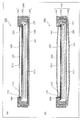
- FIG. 1 is an external perspective view of the liquid crystal display device according to Embodiment 1.
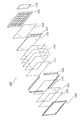
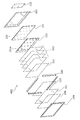
- FIG. FIG. 2 is an exploded perspective view of the liquid crystal backlight device according to the first embodiment.
- FIG. 3 is a cross-sectional view of the liquid crystal backlight device according to the first embodiment.
- FIG. 4 is an exploded perspective view showing an example of the arrangement of the cushion members.
- FIG. 5 is a schematic diagram illustrating an example of a vacuum bonding process between the touch panel and the liquid crystal backlight device.
- FIG. 6 is a cross-sectional view for explaining a problem during vacuum bonding in a liquid crystal backlight device having a conventional configuration.
- FIG. 7 is a diagram illustrating an internal configuration of a chamber for fixing the touch panel and the backlight device at appropriate positions.
- FIG. 8 is an exploded perspective view of the liquid crystal backlight device according to the second embodiment.
- FIG. 9 is a cross-sectional view of the liquid crystal backlight device according to the second embodiment.
- the touch panel and the liquid crystal module are separate parts, and the liquid crystal module is mounted inside the casing, and the touch panel is mounted on the front side of the casing as a part of the exterior. For this reason, it has been common until now that an air layer is interposed between the touch panel and the liquid crystal module.
- direct bonding a technology for directly bonding a touch panel and a liquid crystal module
- some products have already started to spread in the market.
- direct bonding various merit such as suppression of reflection, improvement of brightness, improvement of strength, prevention of dew condensation, prevention of dust mixing can be expected.
- This disclosure relates to a bonding technique in a vacuum environment among bonding techniques in direct bonding.
- a touch panel and a liquid crystal module are bonded together, there are two possible combinations of components to be bonded.
- One is a method of bonding the touch panel and the liquid crystal module as they are.
- the other is that before assembling the liquid crystal module itself, the part of the liquid crystal cell to be incorporated into the liquid crystal module is extracted first, the touch panel and the liquid crystal cell are bonded together, and after bonding, other parts of the liquid crystal module (for example, the back surface) Light).
- the former is easy to implement when the LCD module is not assembled in-house.
- it is necessary to assemble a backlight separately in the latter it is necessary to consider the process of assembling the backlight for implementation. For this reason, there are many places where service manufacturers that perform bonding mainly perform the former method.
- the liquid crystal module often has a structure in which the exterior is structurally completely sealed in order to prevent dust from entering the inside. That is, the liquid crystal module is not provided with a hole or the like leading to the inside of the liquid crystal module except in a special case. This is because if the hole is provided in the liquid crystal module, dust easily enters the liquid crystal module from the hole. Once the dust enters the liquid crystal module, the dust is reflected on the display, and it is difficult to remove the dust, leading to a serious defect as a product.
- both the touch panel and the liquid crystal module are placed in a vacuum chamber, and the vacuum chamber is depressurized to increase the degree of vacuum and then bonded.
- the vacuum chamber is depressurized to increase the degree of vacuum and then bonded.
- a pressure difference is generated between the inside of the liquid crystal module and the outside (inside the vacuum chamber), so that the liquid crystal module swells (see FIG. 5 described later).
- the alignment between the liquid crystal module and the touch panel is performed after setting the workpiece, and the process of vacuum bonding is performed after the alignment.
- the liquid crystal module and the touch panel are misaligned, resulting in a serious defect in the process.
- the vacuum chamber suddenly depressurizes to around 100 Pa in a few seconds to a few tens of seconds. Due to this sudden depressurization, a pressure difference occurs between the inside and the outside of the liquid crystal module.
- it is a structurally sealed liquid crystal module, it is assembled with parts, so a slight gap is formed between the parts, and in a vacuum environment, air enters and exits slightly through the gap. To do.
- the liquid crystal module is left in a vacuum environment for a long time (about several tens of minutes), the pressure difference between the inside and the outside of the liquid crystal module is gradually reduced, and the swelling of the liquid crystal module is also settled.
- the mass productivity is remarkably lowered and the cost is also affected.
- This disclosure solves such a problem.
- FIG. 1 is an external perspective view of the liquid crystal display device according to the present embodiment.
- the liquid crystal display device 10 includes a touch panel (touch screen) 130 on which a touch sensor is arranged, and a liquid crystal backlight device 100 as a liquid crystal module.
- the liquid crystal display device 10 may be configured to include a cover glass instead of the touch panel 130, or may be configured to have a cover glass disposed on the upper surface of the touch panel 130.
- the touch panel 130 is disposed on the front side of the liquid crystal backlight device 100.
- the liquid crystal display device 10 is a smartphone, a tablet, a laptop PC, a desktop PC, various monitor devices, or the like.
- FIG. 2 is an exploded perspective view of the liquid crystal backlight device according to the present embodiment.
- FIG. 3 is a cross-sectional view of the liquid crystal backlight device according to the present embodiment.
- the liquid crystal backlight device 100 includes a liquid crystal panel 101, an optical sheet 102, a light guide plate 103, a frame 120, a light source 107, a reflection sheet 108, and a circuit board 112. Prepare.
- the frame 120 includes a first frame 106 having an opening and a second frame 105 forming a space with the first frame 106.
- the frame 120 is a member that constitutes a housing of the liquid crystal backlight device 100.
- the frame 120 is made of resin or metal.
- the first frame 106 is disposed on the front surface side, and includes a front surface portion 106a in which an opening 106b is formed, and a side wall portion 106c that is connected to the outer peripheral portion of the front surface portion 106a and surrounds the side of the light guide plate 103. It is a letter-shaped member.
- the front part 106 a of the first frame 106 supports the back side of the outer peripheral part of the liquid crystal panel 101 and presses the front side of the outer peripheral part of the optical sheet 102 and the light guide plate 103. Further, a hole 106d penetrating the side wall 106c is formed in the side wall 106c of the first frame 106.
- the second frame 105 is connected to the back surface portion 105a disposed on the back surface side of the light guide plate 103 and the outer peripheral portion of the back surface portion 105a, and covers the side surfaces of the light guide plate 103 and the side wall portion 106c of the first frame 106. 105b.
- an optical sheet 102, a light source 107, and a reflective sheet 108 are accommodated in a space formed by the first frame 106 and the second frame 105.
- a hole 105c penetrating the side wall 105b is formed in the side wall 105b of the second frame 105.
- the frame 120 may further include a front frame 104 that covers the front side of the first frame 106.
- the front frame 104 is disposed on the front surface side of the first frame 106 and includes a front surface portion 104 a having an opening 104 b and a side wall portion 104 c that covers the side of the side wall portion 105 b of the second frame 105.
- the front part 104a is a part that presses the outer peripheral part of the liquid crystal panel 101 from the front side.
- a hole 104d penetrating the side wall 104c is formed in the side wall 104c of the front frame 104.
- the front frame 104 may be made of resin or metal like the first frame 106 and the second frame 105, or may be made of tape.
- the holes (holes 104d, 105c, 106d) formed on the side surface of the frame 120 are provided on the side surface of the frame 120 opposite to the side where the light source 107 is disposed. For this reason, it can reduce that ventilation in a hole by light source 107 is controlled.
- the holes are preferably larger than the gap between the space inside the frame 120 and the space outside the frame 120 and the liquid crystal panel 101. For this reason, when the liquid crystal backlight device is placed in a vacuum environment, the pressure difference between the space inside the liquid crystal backlight device and the space outside can be efficiently eliminated.
- the liquid crystal panel 101 is a display panel for video display in which a plurality of pixels are arranged in a matrix.
- the liquid crystal panel 101 is disposed on the back side of the first frame 106 (that is, the side opposite to the second frame 105), and closes the opening of the first frame 106.
- the liquid crystal panel 101 displays a video based on a video signal input to a drive circuit (not shown).
- the optical sheet 102 is a sheet that is disposed between the first frame 106 and the light guide plate 103 and has various optical functions.
- the optical sheet 102 includes, for example, a diffusion sheet that improves the uniformity of brightness by diffusing light, and a prism sheet that improves the brightness visually recognized by the user by aligning the light path in the front direction.
- the optical sheet 102 may include a microlens, a brightness enhancement sheet, a composite sheet, and the like.
- the optical sheet 102 is made of, for example, a molding resin having a fine shape corresponding to its function on the surface.
- the light guide plate 103 is a member that guides light emitted from the light source 107 arranged on the side toward the front (that is, the liquid crystal panel 101 and the optical sheet 102).
- the light guide plate 103 is made of, for example, polycarbonate (PC), polymethacrylstyrene (MS), methacrylic resin (PMMA), or the like.
- the light source 107 includes a long substrate and a plurality of LEDs (Light Emitting Diodes) arranged on the substrate in the longitudinal direction of the substrate.
- the light guide plate 103 and the light source 107 constitute a backlight unit that is disposed in the space of the frame 120 and emits light to the liquid crystal panel 101.
- the cushion member 109 is an elastic member that is disposed between the front frame 104 and the liquid crystal panel 101 and protects the front surface of the liquid crystal panel 101.
- the circuit board 112 is disposed on the back side of the second frame 105.
- the circuit board 112 is, for example, a circuit board provided with a signal processing circuit that receives a video signal and processes the video signal, a power supply circuit for supplying operating power to the liquid crystal backlight device 100, and the like.
- the number of circuit boards 112 is one, but they may be divided into a plurality of sheets according to the type of circuit.
- the cushion member 110 is a first elastic member disposed between the liquid crystal panel 101 and the first frame 106 so as to surround the opening 106 b of the first frame 106 without a gap.
- FIG. 4 is an exploded perspective view showing an example of the arrangement of the cushion members.
- the cushion member 110 is a member that protects the back surface of the liquid crystal panel 101.
- the cushion member 111 is a plurality of second elastic members that are disposed between the first frame 106 and the optical sheet 102 so as to surround the opening 106b of the first frame 106 and at a predetermined interval.
- the cushion member 111 is a member that protects the front surface of the optical sheet 102.
- the cushion members 109 to 111 are, for example, sponge-like members formed by foaming resin.
- the front side of the opening 106 b of the first frame 106 is blocked by the liquid crystal panel 101 via the cushion member 110. Since the cushion member 110 is disposed so as to surround the front side of the opening 106b without any gap, the liquid crystal panel 101 is in a state of sealing the front side of the opening 106b.
- the cushion member 111 is a plurality of cushion members that surround the opening 106b on the back side of the opening 106b and are disposed with a predetermined interval of the opening 111a. That is, in the portion of the opening 111a of the cushion member 111, a space is provided for communicating the first space S1 between the liquid crystal panel 101 and the optical sheet 102 and the second space S2 in which the light guide plate 103 is disposed. It can be said that. In this embodiment, four openings 111a are provided. However, the number of openings 111a is not limited to four, and may be one, two, three, five, or more.
- the holes (holes 104d, 105c, 106d) formed on the side surface of the frame 120 are sealed with a sealing material 113. For this reason, by removing the sealing material 113, the space inside the frame 120 and the space outside can be easily communicated.
- the sealing material 113 shields light between the external space and the space inside the frame 120 in the hole. Thereby, it is possible to reduce leakage of light emitted from the light source of the liquid crystal backlight device 100 to the outside of the frame 120.
- the sealing material 113 is comprised by the adhesive tape, for example. Thereby, immediately before performing bonding in a vacuum environment, the sealing material can be easily removed while suppressing entry of dust into the space inside the frame 120.
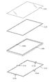
- FIG. 5 is a schematic view showing an example of a bonding process between the touch panel (or cover glass) and the liquid crystal backlight device.
- a first inspection process for inspecting the foreign material on the surface of the material and confirming scratches is performed for each of the touch panel 301 and the liquid crystal backlight device 302.
- FIG. 5B shows two typical application methods.
- One of the two types of application methods is a dam and fill method in which the adhesive 304 is applied using the dispenser 303 (see the upper part of FIG. 5B).
- the other is a method called slit coating in which an adhesive 304 is applied using a slit coater 305 and semi-cured with a temporary curing UV 306 immediately after application.
- the next process shown in FIG. 5C is a bonding process.
- the bonding step is performed in a vacuum environment, specifically, in a chamber 307 that can be depressurized to a vacuum state.
- the touch panel 301 and the liquid crystal backlight device 302, which are adherends are fixed in the chamber facing each other, decompressed, and a vacuum state is created in the chamber. Then, the adherend with two adhesives is bonded together.
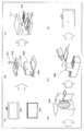
- FIG. 6 is a diagram illustrating an internal configuration of a chamber for fixing the touch panel and the liquid crystal backlight device at appropriate positions.
- the first regulating unit 307a regulates movement of the long side and the short side of the touch panel 301 and the liquid crystal backlight device 302 when viewed from above.
- the 1st control part 307a is being fixed to the chamber 307, and is an L-shaped wall in the top view.
- the 2nd control part 307b is arrange
- the second restricting portion 307b is also fixed to the chamber 307 similarly to the first restricting portion 307a.
- the plurality of pressing portions 307c are arranged on the first restriction portion 307a side of the second restriction portion 307b, and the long side and short side surfaces on the other side of the touch panel 301 and the liquid crystal backlight device 302 are arranged on the first restriction portion 307a. Hold it down.
- the plurality of pressing portions 307c press the touch panel 301 and the liquid crystal backlight device 302 toward the first restricting portion 307a, for example, with a force that a compressed compression spring is about to extend.
- the side surfaces of the touch panel 301 and the liquid crystal backlight device 302 are pressed by the first restricting portion 307a or the pressing portion 307c.
- the hole that connects the space inside the frame 120 and the space outside is provided only on the side surface of the frame 120. Thereby, it is possible to reduce the suppression of the air flow in the holes (holes 104d, 105c, 106d) of the frame 120 by the device for fixing the adherend when performing the bonding.
- the next step is a pressurizing step in which the touch panel 301 and the liquid crystal backlight device 302 adhered in a vacuum environment are placed in the autoclave 308 as shown in FIG.
- the pressurizing step only the pressurization may be performed by inserting the touch panel 301 and the liquid crystal backlight device 302 bonded to the autoclave 308 in which the internal space is a high-pressure environment, or a temperature may be applied. Thereby, the air bubbles mixed in the bonding process can be dispersed and dissolved in the adhesive.
- the pressurizing step may not be performed depending on the type of adhesive and the application method.
- the next process is a UV irradiation process in which the bonded touch panel 301 and the liquid crystal backlight device 302 are passed through a UV irradiation machine 309 as shown in FIG.
- the UV irradiation process is performed only when the adhesive is a UV curable adhesive or adhesive.
- the next step is a second inspection step for inspecting whether the appearance of the bonded touch panel 301 and the liquid crystal backlight device 302 is abnormal as shown in FIG.
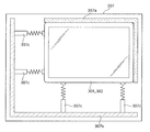
- FIG. 7 is a cross-sectional view for explaining a problem during vacuum bonding in a liquid crystal backlight device having a conventional configuration.
- FIG. 7A is a schematic view of a state of the liquid crystal module under atmospheric pressure (that is, a state before being in a vacuum state).
- FIG. 7B is a schematic diagram showing a state of the liquid crystal module when the pressure is rapidly reduced to a vacuum state. That is, FIG. 7 is a diagram for explaining a change in a liquid crystal backlight device having a conventional configuration before and after decompression.
- the liquid crystal backlight device 200 having the conventional configuration is different from the liquid crystal backlight device 100 in the structure of the frame 140 and the arrangement of the cushion member 111. Specifically, no through hole is formed in the side wall of the frame 140, and the space formed by the liquid crystal panel 101, the frame 140, and the cushion member 109 is sealed from the outside.
- the frame 140 includes a front frame 141, a first frame 142, and a second frame 143 that are not formed with through holes.
- the first space S11 surrounded by the liquid crystal panel 101 and the optical sheet changes before and after the decompression.
- Each of the first space S ⁇ b> 11 and the second space S ⁇ b> 12 is a separately independent closed space inside the liquid crystal backlight device 200. That is, the first space S ⁇ b> 11 and the second space S ⁇ b> 12 are spaces that are also closed from the outside of the liquid crystal backlight device 200.
- a general liquid crystal backlight device is different in size between the first space S11 and the second space S12 depending on the type, and the first space S11 and the second space S12.
- the liquid crystal backlight device 200 may include a part of the reflective sheet 108 and the light guide plate 103 bonded together by a double-sided adhesive tape or the like. However, there is nothing that is bonded together.
- the first space S11 and the second space S12 formed inside the liquid crystal backlight device 200 are used when the outside of the liquid crystal backlight device 200 is suddenly depressurized in a vacuum bonding process, for example.
- the space (the first space S11 and the second space S12) inside the liquid crystal backlight device 200 is expanded.
- the liquid crystal backlight device 200 is in a swelled state. Therefore, when the bonding process between the touch panel and the liquid crystal backlight device 200 described in FIG. 5C is performed in a state where the liquid crystal backlight device 200 is swollen, the liquid crystal backlight device 200 and the touch panel are in surface contact. Therefore, the touch panel cannot be accurately placed at an appropriate position of the liquid crystal backlight device 200.
- the bonding process shown in FIG. 5C is performed in a clean room. Therefore, when the touch panel 130 is bonded to the liquid crystal backlight device 100, the sealing material 113 is opened immediately before the bonding process. In this way, by removing the sealing material 113, the space inside the frame 120 and the space outside can be easily communicated. In this state, the liquid crystal backlight device 100 and the touch panel 130 are aligned, and bonding is performed in the chamber 307. After the bonding is completed, the hole formed in the side surface of the frame 120 is sealed again with the sealing material 113.
- the sealing material used at this time may be the sealing material attached to the liquid crystal backlight device 100 before bonding, or may be another sealing material. The present disclosure is not limited to this. By doing so, foreign matter can be prevented from entering the liquid crystal backlight device 100, and the problem that the liquid crystal backlight device expands inside the chamber 307 can be solved.
- the cushion member 111 composed of a plurality of second elastic members surrounds the opening 106b of the first frame 106 and is disposed with the opening 111a at a predetermined interval. Therefore, the space formed by the frame 120 can be in a state where it is not separated by the optical sheet 102 and the cushion member 111. That is, the first space S1 between the liquid crystal panel 101 and the optical sheet 102 and the second space S2 between the optical sheet 102 and the second frame 105 can be brought into communication.
- the liquid crystal backlight device 100 can be removed from the hole until the sealing material 113 is removed in the bonding in a vacuum environment. It is possible to suppress the entry of garbage into the internal space.
- Embodiment 2 In the liquid crystal backlight device 100 according to Embodiment 1, it is assumed that the backlight unit is an edge light type backlight including the light guide plate 103 and the light source 107 disposed on the side thereof.
- the present invention is not limited to the above configuration, and for example, as shown in FIGS. 8 and 9, a liquid crystal backlight device 400 that employs a direct type backlight unit in which a light source is disposed on the back side of the liquid crystal panel 101 may be used.
- FIG. 8 is an exploded perspective view of the liquid crystal display device according to the second embodiment.
- FIG. 9 is a cross-sectional view of the liquid crystal backlight device according to the second embodiment.
- the liquid crystal backlight device 400 according to Embodiment 2 includes a reflective sheet 151 and a light source 152 instead of the edge light type backlight configured by the light guide plate 103, the light source 107, and the reflective sheet 108 of the liquid crystal backlight device 100.
- the difference from the liquid crystal backlight device 100 according to Embodiment 1 is that a direct-type backlight configured is employed.
- the shapes of the front frame 204, the first frame 206, and the second frame 205 are different from those of the front frame 104, the first frame 106, and the second frame 105 of the first embodiment.
- the second frame 205 has a shape along the inclined portion 151 b that forms the end of the reflection sheet 151.
- the front frame 204, the first frame 206, and the second frame 205 are different in shape, but the parts having the same functions as those of the front frame 104, the first frame 106, and the second frame 105 are replaced with reference numerals in the 100s. Swinging in the 200s. For this reason, the detailed description in the said part is abbreviate
- the light source 152 is provided on the back side of the liquid crystal panel 101, has a plurality of LEDs 153 arranged in a matrix on the main surface on the front side, and irradiates light emitted from the plurality of LEDs from the back side of the liquid crystal panel 101.
- the light source 152 is disposed at a predetermined interval from the optical sheet 102 in order to diffuse the light emitted from the light source 152 toward the liquid crystal panel.
- the reflection sheet 151 is a sheet that is disposed on the front side of the light source 152 and reflects the light emitted from the light source 152 toward the front surface.
- the reflective sheet 151 has a plurality of openings 151 a that expose the plurality of LEDs 153 at positions corresponding to the plurality of LEDs 153.
- the reflection sheet 151 includes an inclined portion 151 b that reflects light emitted from the light source 152 toward the center of the liquid crystal panel 101 at the end of the liquid crystal panel 101.
- the second frame 205 has a shape that follows the shape of the reflective sheet 151, and has an inclined portion 205a that supports the inclined portion 151b on a plane. Since the inclined portion 205a is formed in the second frame 205, the reflective sheet 151 can maintain the inclined portion 151b in an inclined state.
- the light source 152 is arranged at a predetermined interval from the optical sheet 102, and the reflective sheet 151 and the second frame 205 are formed with the inclined portions 151b and 205a.
- a second space S22 is formed between the sheet 102 and the reflection sheet 151 and the light source 152 constituting the backlight unit.
- the second space S22 is formed by supporting the optical sheet 102 by the reflection sheet 151 and the inclined portions 151b and 205a of the second frame 205. Therefore, when the hole is not formed, the second space S22 is a closed space. It becomes.
- a first space S21 similar to the first space S1 of the first embodiment is also formed between the liquid crystal panel 101 and the optical sheet 102.
- the liquid crystal backlight device 400 that employs a direct type backlight, the first space S21 and the second space S22 are formed, and therefore no holes are formed in the frame 220 or the backlight unit. In this case, a problem similar to that of the liquid crystal backlight device 200 employing the edge light type backlight occurs.
- the holes 204d and 206d serving as the first holes for communicating the first space S21 and the external space are formed as the side wall portion 104c and the first frame 206 of the front frame 204. Are provided on the side wall portions 206c.
- the holes 204d and 206d as the first holes are provided on the side surface of the first frame 206 when viewed from the arrangement direction of the first frame 206 and the second frame 205, and between the liquid crystal panel 101 and the optical sheet. It is a through-hole which connects 1st space S21 of this, and external space.
- holes 151c and 205b as second holes for communicating the second space S22 and the external space are provided in the reflecting sheet 151 and the inclined portions 151b and 205a of the second frame 205, respectively. That is, the holes 151c and 205b as the second holes are provided on the side surfaces (inclined portions 151b and 205a) of the backlight unit and the second frame 205, and the second between the backlight unit and the optical sheet 102 is provided. It is a through-hole which connects space S22 and external space.
- the liquid crystal backlight device 400 is provided with sealing materials 113A and 113B for sealing the holes 204d and 206d as the first holes and the holes 151c and 205b as the second holes, respectively.
- the configuration of the frame 120 is the same as that of the liquid crystal backlight device 100 according to the first embodiment. The same effect as 100 is produced.
- the sealing material 113 is composed of an adhesive tape, but is not limited to an adhesive tape, and may be a cap that seals the hole by being press-fitted into the hole. Moreover, the hole may be threaded and the bolt which seals a hole by screwing with a hole may be sufficient.
- the present disclosure is applicable to a liquid crystal backlight device that is vacuum-bonded to a cover glass (or touch panel or the like).
Abstract
Description
本発明者は、「背景技術」の欄において記載した従来のタッチパネル付き液晶表示装置に関し、以下の問題が生じることを見出した。 (Knowledge that became the basis of the present invention)
The inventor has found that the following problems occur with respect to the conventional liquid crystal display device with a touch panel described in the “Background Art” column.
以下、図1~図4を用いて、実施の形態1について説明する。 (Embodiment 1)
Hereinafter, the first embodiment will be described with reference to FIGS.
図2は、本実施の形態に係る液晶バックライト装置の分解斜視図である。図3は、本実施の形態に係る液晶バックライト装置の断面図である。 [1. Configuration of LCD backlight device]
FIG. 2 is an exploded perspective view of the liquid crystal backlight device according to the present embodiment. FIG. 3 is a cross-sectional view of the liquid crystal backlight device according to the present embodiment.
次に図5を用いて代表的な真空貼り合わせプロセスについて説明する。 [2. Vacuum bonding process]
Next, a typical vacuum bonding process will be described with reference to FIG.
ここで図7を用いて、真空貼り合わせ時の液晶モジュールの膨張課題について詳しく説明する。図7は、従来の構成の液晶バックライト装置における真空貼合時の課題を説明するための断面図である。具体的には、図7の(a)は、大気圧下での液晶モジュールの状態(つまり真空状態にする前の状態)の概略図である。また、図7の(b)は、真空状態に急減圧した場合の液晶モジュールの状態を示した概略図である。つまり、図7は、減圧の前後における従来の構成の液晶バックライト装置の変化を説明するための図である。 [3. Expansion location of LCD backlight device in vacuum bonding process]
Here, the expansion | swelling subject of the liquid crystal module at the time of vacuum bonding is demonstrated in detail using FIG. FIG. 7 is a cross-sectional view for explaining a problem during vacuum bonding in a liquid crystal backlight device having a conventional configuration. Specifically, FIG. 7A is a schematic view of a state of the liquid crystal module under atmospheric pressure (that is, a state before being in a vacuum state). FIG. 7B is a schematic diagram showing a state of the liquid crystal module when the pressure is rapidly reduced to a vacuum state. That is, FIG. 7 is a diagram for explaining a change in a liquid crystal backlight device having a conventional configuration before and after decompression.
本実施の形態に係る液晶バックライト装置100によれば、複数の第2弾性部材により構成されるクッション部材111が第1フレーム106の開口106bを囲み、かつ、所定間隔の開口111aを空けて配置されているため、フレーム120が形成している空間を光学シート102及びクッション部材111で分離されていない状態とすることができる。つまり、液晶パネル101及び光学シート102の間の第1空間S1と、光学シート102及び第2フレーム105の間の第2空間S2とを連通させた状態とすることができる。また、フレーム120の側方側の側面に、フレーム120の内部の空間と外部の空間とを連通する孔を形成しているため、孔が封止材113により封止されていない状態では、第1空間S1、第2空間S2及び外部とが連通された状態にできる。このため、孔を封止している封止材113を取り除いた後で、真空環境下において、当該液晶バックライト装置100と、タッチパネル130との貼り合わせを行えば、液晶バックライト装置100の内部の空間とチャンバー307の内部の空間との間に圧力差が生じることを低減できる。 [4. effect]
According to the liquid
実施の形態1に係る液晶バックライト装置100では、バックライトユニットが、導光板103及びその側方に配置される光源107により構成されるエッジライト型バックライトであるとした。しかし、上記の構成に限らずに、例えば、図8及び図9に示すように、光源が液晶パネル101の背面側に配置される直下型のバックライトユニットを採用した液晶バックライト装置400としてもよい。なお、図8は、実施の形態2に係る液晶表示装置の分解斜視図である。図9は、実施の形態2に係る液晶バックライト装置の断面図である。 (Embodiment 2)
In the liquid
上記実施の形態1では、封止材113は、粘着テープにより構成されるとしたが、粘着テープに限らずに、孔に圧入されることで孔を封止するキャップであってもよい。また、孔がねじ切られており、孔と螺合することにより孔を封止するボルトであってもよい。 (Other embodiments)
In
100、200、400 液晶バックライト装置
101 液晶パネル
102 光学シート
103 導光板
104、141、204 前面フレーム
104a 前面部
104b 開口
104c 側壁部
104d、204d 孔
105、143、205 第2フレーム
105a 背面部
105b 側壁部
105c、205c 孔
106、142、206 第1フレーム
106a 前面部
106b 開口
106c、206c 側壁部
106d、206d 孔
107、152 光源
108、151 反射シート
109~111 クッション部材
111a 開口
112 回路基板
113 封止材
120、140、220 フレーム
130 タッチパネル
151a 開口
151b 傾斜部分
151c 孔
153 LED
205a 傾斜部分
301 タッチパネル(もしくはカバーガラス)
302 液晶バックライト装置
303 ディスペンサー
304 接着剤
305 スリットコーター
306 仮硬化用UV
307 チャンバー
307a 第1規制部
307b 第2規制部
307c 押さえ部
308 オートクレーブ
309 UV照射機
S1、S11、S21 第1空間
S2、S12、S22 第2空間
S23 第3空間 10 Liquid
205a
302 Liquid
Claims (7)
- 開口を有する第1フレームと、前記第1フレームとで空間を形成している第2フレームとを有するフレームと、
前記第1フレームの、前記第2フレームとは反対側に配置され、前記開口を塞ぐ液晶パネルと、
前記空間に配置され、前記液晶パネルに光を照射するバックライトユニットと、
前記第1フレームと前記バックライトユニットとの間に配置される光学シートと、
前記液晶パネルと前記第1フレームとの間において、前記第1フレームの前記開口を隙間なく囲んで配置される第1弾性部材と、
前記第1フレームと前記光学シートとの間において、前記第1フレームの前記開口を囲み、かつ、所定間隔を空けて配置される複数の第2弾性部材と、
前記第1フレーム及び前記第2フレームの並び方向から見て、前記フレームの側方側の側面に設けられた、前記空間と外部とを連通する孔を封止する封止材と、を備える
液晶バックライト装置。 A frame having a first frame having an opening, and a second frame forming a space with the first frame;
A liquid crystal panel disposed on the opposite side of the first frame to the second frame and closing the opening;
A backlight unit disposed in the space and irradiating the liquid crystal panel with light;
An optical sheet disposed between the first frame and the backlight unit;
A first elastic member disposed between the liquid crystal panel and the first frame so as to surround the opening of the first frame without a gap;
Between the first frame and the optical sheet, a plurality of second elastic members that surround the opening of the first frame and are arranged at a predetermined interval;
A sealing material that is provided on a side surface on a side of the frame as viewed from the arrangement direction of the first frame and the second frame and seals a hole that communicates the space and the outside. Backlight device. - 前記封止材は、前記孔において外部と前記空間との間を遮光している
請求項1に記載の液晶バックライト装置。 The liquid crystal backlight device according to claim 1, wherein the sealing material shields light between the outside and the space in the hole. - 前記封止材は、粘着テープにより構成されている
請求項1または2に記載の液晶バックライト装置。 The liquid crystal backlight device according to claim 1, wherein the sealing material is made of an adhesive tape. - 前記バックライトユニットは、
前記空間の端部に配置される光源と、
前記光源が発した光を前記液晶パネル及び前記光学シートに向けて導く導光板と、を有し、
前記孔は、前記フレームの、前記光源が配置される側とは反対側の前記側面に設けられている
請求項1から3のいずれか1項に記載の液晶バックライト装置。 The backlight unit is
A light source disposed at an end of the space;
A light guide plate for guiding the light emitted from the light source toward the liquid crystal panel and the optical sheet,
The liquid crystal backlight device according to any one of claims 1 to 3, wherein the hole is provided on the side surface of the frame opposite to a side on which the light source is disposed. - 前記孔は、前記フレームの前記側面のみに設けられている
請求項1から4のいずれか1項に記載の液晶バックライト装置。 The liquid crystal backlight device according to claim 1, wherein the hole is provided only in the side surface of the frame. - 前記孔は、前記フレーム及び前記液晶パネルが有する、前記空間と外部との間の隙間より大きい
請求項1から5のいずれか1項に記載の液晶バックライト装置。 The liquid crystal backlight device according to any one of claims 1 to 5, wherein the hole is larger than a gap between the space and the outside of the frame and the liquid crystal panel. - 開口を有する第1フレームと、前記第1フレームとで空間を形成している第2フレームとを有するフレームと、
前記第1フレームの、前記第2フレームとは反対側に配置され、前記開口を塞ぐ液晶パネルと、
前記空間に配置され、前記液晶パネルに光を照射するバックライトユニットと、
前記第1フレームと前記バックライトユニットとの間に配置される光学シートと、
前記液晶パネルと前記第1フレームとの間において、前記第1フレームの前記開口を隙間なく囲んで配置される第1弾性部材と、
前記第1フレームと前記光学シートとの間において、前記第1フレームの前記開口を囲み、かつ、所定間隔を空けて配置される複数の第2弾性部材と、
前記第1フレーム及び前記第2フレームの並び方向から見て、前記第1フレームの側方側の側面に設けられ、前記液晶パネル及び前記光学シートの間の第1空間と外部の空間とを連通する第1孔と、前記バックライトユニット及び前記第2フレームの側方側の側面に設けられ、前記バックライトユニット及び前記光学シートの間の第2空間と外部の空間とを連通する第2孔とを封止する封止材と、を備える
液晶バックライト装置。 A frame having a first frame having an opening, and a second frame forming a space with the first frame;
A liquid crystal panel disposed on the opposite side of the first frame to the second frame and closing the opening;
A backlight unit disposed in the space and irradiating the liquid crystal panel with light;
An optical sheet disposed between the first frame and the backlight unit;
A first elastic member disposed between the liquid crystal panel and the first frame so as to surround the opening of the first frame without a gap;
Between the first frame and the optical sheet, a plurality of second elastic members that surround the opening of the first frame and are arranged at a predetermined interval;
The first space between the liquid crystal panel and the optical sheet is provided on the side surface of the first frame when viewed from the direction in which the first frame and the second frame are arranged, and communicates with the external space. A second hole that is provided on a side surface of the backlight unit and the second frame and communicates with a second space between the backlight unit and the optical sheet and an external space. And a sealing material for sealing the liquid crystal backlight device.
Priority Applications (3)
| Application Number | Priority Date | Filing Date | Title |
|---|---|---|---|
| JP2017545771A JP6671044B2 (en) | 2016-03-10 | 2016-08-24 | LCD backlight device |
| EP16893381.0A EP3410180B1 (en) | 2016-03-10 | 2016-08-24 | Liquid crystal backlight device |
| US15/802,323 US10330976B2 (en) | 2016-03-10 | 2017-11-02 | Liquid crystal backlight device |
Applications Claiming Priority (2)
| Application Number | Priority Date | Filing Date | Title |
|---|---|---|---|
| JP2016-047401 | 2016-03-10 | ||
| JP2016047401 | 2016-03-10 |
Related Child Applications (1)
| Application Number | Title | Priority Date | Filing Date |
|---|---|---|---|
| US15/802,323 Continuation US10330976B2 (en) | 2016-03-10 | 2017-11-02 | Liquid crystal backlight device |
Publications (1)
| Publication Number | Publication Date |
|---|---|
| WO2017154049A1 true WO2017154049A1 (en) | 2017-09-14 |
Family
ID=59790148
Family Applications (1)
| Application Number | Title | Priority Date | Filing Date |
|---|---|---|---|
| PCT/JP2016/003848 WO2017154049A1 (en) | 2016-03-10 | 2016-08-24 | Liquid crystal backlight device |
Country Status (4)
| Country | Link |
|---|---|
| US (1) | US10330976B2 (en) |
| EP (1) | EP3410180B1 (en) |
| JP (1) | JP6671044B2 (en) |
| WO (1) | WO2017154049A1 (en) |
Families Citing this family (6)
| Publication number | Priority date | Publication date | Assignee | Title |
|---|---|---|---|---|
| JP6265254B1 (en) * | 2016-12-15 | 2018-01-24 | オムロン株式会社 | Inspection apparatus and inspection method |
| KR102266209B1 (en) * | 2017-04-29 | 2021-06-16 | 엘지디스플레이 주식회사 | Display apparatus |
| CN108761912A (en) * | 2018-05-31 | 2018-11-06 | 江苏聚泰科技有限公司 | A kind of shockproof backlight module |
| CN109459880B (en) * | 2018-12-11 | 2021-04-30 | 厦门天马微电子有限公司 | Display module and display device |
| JP6991448B2 (en) * | 2018-12-20 | 2022-02-03 | トライベイル テクノロジーズ, エルエルシー | Display device |
| CN212723610U (en) * | 2020-09-28 | 2021-03-16 | 京东方科技集团股份有限公司 | Backlight module and display device |
Citations (4)
| Publication number | Priority date | Publication date | Assignee | Title |
|---|---|---|---|---|
| JPH07168177A (en) * | 1993-12-15 | 1995-07-04 | Canon Inc | Liquid crystal display device |
| JP2005062777A (en) * | 2003-08-20 | 2005-03-10 | Sharp Corp | Display device |
| JP2005108769A (en) * | 2003-10-01 | 2005-04-21 | Sumitomo Rubber Ind Ltd | Directly underlying backlight |
| JP2007059181A (en) * | 2005-08-24 | 2007-03-08 | Sony Corp | Optical device and manufacturing method therefor |
Family Cites Families (11)
| Publication number | Priority date | Publication date | Assignee | Title |
|---|---|---|---|---|
| DE69423552T2 (en) | 1993-08-10 | 2000-09-07 | Canon Kk | Liquid crystal display |
| JP2001264754A (en) * | 2000-03-15 | 2001-09-26 | Nec Corp | Liquid crystal display device and light source device used for the same |
| JP3620840B2 (en) * | 2002-07-17 | 2005-02-16 | シャープ株式会社 | Liquid crystal display |
| JP4260519B2 (en) * | 2003-03-31 | 2009-04-30 | シャープ株式会社 | Liquid crystal display |
| TWI384300B (en) * | 2006-10-11 | 2013-02-01 | Tpo Displays Corp | Display panel module |
| JP4713622B2 (en) * | 2008-09-19 | 2011-06-29 | 株式会社日立製作所 | Liquid crystal display device and video display device using the same |
| KR101267084B1 (en) * | 2009-02-23 | 2013-05-23 | 엘지디스플레이 주식회사 | Liquid crystal module |
| WO2011162019A1 (en) * | 2010-06-22 | 2011-12-29 | シャープ株式会社 | Display panel and display device |
| US9081429B2 (en) * | 2011-12-16 | 2015-07-14 | Htc Corporation | Touch control device |
| JP2014130290A (en) | 2012-12-28 | 2014-07-10 | Panasonic Liquid Crystal Display Co Ltd | Liquid crystal display device with touch panel |
| US20170139102A1 (en) * | 2015-11-13 | 2017-05-18 | Le Holdings(Beijing)Co., Ltd. | Backlight module, and liquid crystal display device |
-
2016
- 2016-08-24 JP JP2017545771A patent/JP6671044B2/en active Active
- 2016-08-24 EP EP16893381.0A patent/EP3410180B1/en active Active
- 2016-08-24 WO PCT/JP2016/003848 patent/WO2017154049A1/en active Application Filing
-
2017
- 2017-11-02 US US15/802,323 patent/US10330976B2/en active Active
Patent Citations (4)
| Publication number | Priority date | Publication date | Assignee | Title |
|---|---|---|---|---|
| JPH07168177A (en) * | 1993-12-15 | 1995-07-04 | Canon Inc | Liquid crystal display device |
| JP2005062777A (en) * | 2003-08-20 | 2005-03-10 | Sharp Corp | Display device |
| JP2005108769A (en) * | 2003-10-01 | 2005-04-21 | Sumitomo Rubber Ind Ltd | Directly underlying backlight |
| JP2007059181A (en) * | 2005-08-24 | 2007-03-08 | Sony Corp | Optical device and manufacturing method therefor |
Also Published As
| Publication number | Publication date |
|---|---|
| US20180059479A1 (en) | 2018-03-01 |
| US10330976B2 (en) | 2019-06-25 |
| JP6671044B2 (en) | 2020-03-25 |
| EP3410180A1 (en) | 2018-12-05 |
| EP3410180B1 (en) | 2019-12-11 |
| JPWO2017154049A1 (en) | 2018-12-27 |
| EP3410180A4 (en) | 2019-01-16 |
Similar Documents
| Publication | Publication Date | Title |
|---|---|---|
| WO2017154049A1 (en) | Liquid crystal backlight device | |
| JP5094250B2 (en) | Display device | |
| CN106019666B (en) | Display device and method for manufacturing display device | |
| JP5254857B2 (en) | Liquid crystal display | |
| JP2018004728A (en) | Display device and bonding method | |
| US9581851B2 (en) | Liquid crystal display device | |
| US20070229726A1 (en) | Liquid crystal display device | |
| US20150286090A1 (en) | Liquid crystal display device and manufacturing method thereof | |
| JP2011075605A (en) | Protective plate integrated display device | |
| JP5487915B2 (en) | Protective plate integrated type liquid crystal display panel manufacturing method | |
| JP2008203319A (en) | Liquid crystal display device, television apparatus and manufacturing method thereof | |
| US20100245703A1 (en) | Liquid crystal display | |
| US8177598B2 (en) | Display manufacturing method | |
| JP2009265237A (en) | Liquid crystal display | |
| KR102064751B1 (en) | Liquid crystal display device having minimized bezzel | |
| CN101726902B (en) | Liquid crystal display device and manufacturing method thereof | |
| JP2007240914A (en) | Method and apparatus for manufacturing electrooptical device | |
| KR100843369B1 (en) | Method for curing sealant using ?? irradiation | |
| JP3847743B2 (en) | Liquid crystal display device manufacturing method | |
| JP2005309332A (en) | Device and method for manufacturing lamination substrate | |
| KR20140101219A (en) | Method of manufacturing liquid crystal display device and sealant curing device used thereto | |
| KR102010850B1 (en) | Method for fabricating liquid crystal panel | |
| KR100500693B1 (en) | Hot press apparatus for fabrication of liquid crystal display cell | |
| JP2009080380A (en) | Liquid crystal device and electronic device | |
| WO2017038519A1 (en) | Lcd device |
Legal Events
| Date | Code | Title | Description |
|---|---|---|---|
| ENP | Entry into the national phase |
Ref document number: 2017545771 Country of ref document: JP Kind code of ref document: A |
|
| WWE | Wipo information: entry into national phase |
Ref document number: 2016893381 Country of ref document: EP |
|
| ENP | Entry into the national phase |
Ref document number: 2016893381 Country of ref document: EP Effective date: 20180831 |
|
| NENP | Non-entry into the national phase |
Ref country code: DE |
|
| 121 | Ep: the epo has been informed by wipo that ep was designated in this application |
Ref document number: 16893381 Country of ref document: EP Kind code of ref document: A1 |