WO2017150574A1 - 双極型静電チャックモジュールおよびその製造方法 - Google Patents
双極型静電チャックモジュールおよびその製造方法 Download PDFInfo
- Publication number
- WO2017150574A1 WO2017150574A1 PCT/JP2017/007987 JP2017007987W WO2017150574A1 WO 2017150574 A1 WO2017150574 A1 WO 2017150574A1 JP 2017007987 W JP2017007987 W JP 2017007987W WO 2017150574 A1 WO2017150574 A1 WO 2017150574A1
- Authority
- WO
- WIPO (PCT)
- Prior art keywords
- electrostatic chuck
- bipolar electrostatic
- module
- bipolar
- chuck module
- Prior art date
- Legal status (The legal status is an assumption and is not a legal conclusion. Google has not performed a legal analysis and makes no representation as to the accuracy of the status listed.)
- Ceased
Links
Images







Classifications
-
- H—ELECTRICITY
- H02—GENERATION; CONVERSION OR DISTRIBUTION OF ELECTRIC POWER
- H02N—ELECTRIC MACHINES NOT OTHERWISE PROVIDED FOR
- H02N13/00—Clutches or holding devices using electrostatic attraction, e.g. using Johnson-Rahbek effect
Definitions
- the present invention relates to a bipolar electrostatic chuck module and a manufacturing method thereof.
- An electrostatic chuck is a device that grips and detaches an object using an electrostatic force acting between the object and the object when a voltage is applied.
- the electrostatic chuck is a mechanism that applies a potential difference between a dielectric layer and a gripping target and attracts the gripping target by generated electrostatic force.
- a Coulomb force type that uses an insulating material as a dielectric.
- Electrostatic chucks are used to hold objects such as silicon wafers that have a flat surface, but the electrostatic force depends on the distance between the electrode and the object, so it is attractive for objects that have a surface shape such as a curved surface. There is a problem that decreases.
- Non-Patent Document 1 An electrostatic chuck with a flexible attracting surface using an integrated structure of electrostatic induction fibers.
- the manufacturing process involves precisely arranging the fibers one by one, making it difficult to increase the area and wire the electrodes.
- the fiber produced by the melt spinning method has irregular tips due to deformation due to residual stress.
- the electrostatic chucks in these existing studies are of a monopolar type, so there is a difficulty that cannot be applied to dielectrics.
- An object of the present invention is to provide a bipolar electrostatic chuck that has a fine bristle structure on an adsorption surface and can be applied to a thin film dielectric such as a plastic sheet. Furthermore, in the present invention, a monolithic electrostatic chuck module is formed by integrally forming three layers with an insulator sandwiched between two conductors, and this module is stacked to increase the area of the fine bristle structure that is the adsorption surface. Is possible.
- the present invention provides the following inventions in order to solve the above problems.
- the electrostatic chuck adsorption surface for adsorbing the object to be adsorbed has a fine bristle structure, and an insulating layer is disposed between the positive electrode and the negative electrode at the tip of the fine hair on the adsorption surface.
- a bipolar electrostatic chuck module configured such that an electrostatic force is generated by applying a voltage and an object to be attracted is attracted to an electrostatic chuck attracting surface.
- a bipolar electrostatic chuck module formed by laminating a plurality of bipolar electrostatic chuck modules according to (1) above.
- fine etching is performed on the tip portion which is the adsorption surface by etching using a conductor.
- Bipolar type in which a beam assembly having a bristle structure is manufactured, the obtained beam assembly is insulation-coated, and then the two insulation-coated beam assemblies are bonded together to form an insulating layer between the positive electrode and the negative electrode
- a bipolar electrostatic chuck module having a fine bristle structure can be provided. Furthermore, according to the present invention, a bipolar electrostatic chuck can be modularized by integrally molding using a 3D printer or lithography technology, and the area of the fine bristle structure can be increased by stacking a plurality of modules. A bipolar electrostatic chuck module having a fine bristle structure capable of gripping a surface having an arbitrary area can be provided. Therefore, according to the present invention, since each module has fine hairs, it is possible to ensure flexibility on the electrostatic adsorption surface, and conventionally it cannot be handled smoothly (even if it can be adsorbed, it cannot be separated well). Can be freely adsorbed and removed.
- FIG. 3 is a diagram illustrating a processing process in the first embodiment.
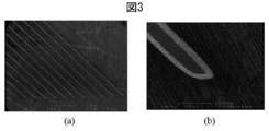
- 2 is a scanning electron microscope (SEM) observation photograph of the beam assembly manufactured in Example 1.
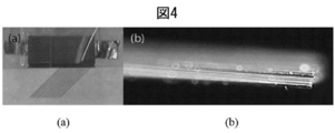
- FIG. 1 shows a bipolar electrostatic chuck module manufactured in Example 1.
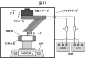
- An experimental system for measuring the attractive force of a bipolar electrostatic chuck is shown.
- a finite element analysis model is shown for evaluating adsorption performance.
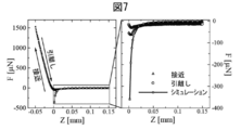
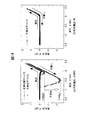
- the force curve of the measured adsorption force and the analysis result by COMSOL are shown.
- the results of the attractive force analysis and measurement in consideration of the tip shape are shown.
- the dimension and external appearance of the module manufactured in Example 2 are shown.
- the lifting test result of the manufactured bipolar electrostatic chuck module is shown.
- Example 3 An outline of an experimental apparatus for measuring a force curve is shown.
- the measurement result of a force curve is shown.
- the fiber tip shape seen by modeling with a 3D printer using an optical modeling method is shown.
- suction part using the heating flat plate in Example 3 is shown.
- blunted are shown.
- the force curve measured about the bipolar electrostatic chuck obtained in Example 3 is shown. It is a schematic diagram which grips, conveys, and peels a thin film such as plastic using the bipolar electrostatic chuck module of the present invention.
- the electrostatic chuck module of the present invention has a fine bristle structure on the electrostatic chuck adsorption surface for adsorbing an object to be adsorbed, and an insulating layer is disposed between the positive electrode and the negative electrode at the tip of the fine hair on the adsorption surface.
- the bipolar electrostatic chuck module is configured such that an electrostatic force is generated by applying a voltage between the positive electrode and the negative electrode, and the object to be attracted is attracted to the electrostatic chuck attracting surface. Since the bipolar electrostatic chuck of the present invention has flexibility on the attracting surface due to the fine bristle structure, it can be delicately gripped by a surface that does not give excessive stress to thin soft materials such as plastic film, paper, and cloth.
- a bipolar electrostatic chuck module laminate formed by laminating a plurality of bipolar electrostatic chuck modules. That is, preferably, a bipolar electrostatic chuck is integrally formed using a 3D printer to form a module, and a plurality of modules are stacked to increase the area of the fine bristle structure. Since the electrostatic chuck module of the present invention is a bipolar type, the dielectric material can be gripped without being energized.
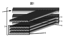
- FIG. 1 is a conceptual diagram of a bipolar electrostatic chuck single-layer module 1 and a bipolar electrostatic chuck (laminated body) 2 having a fine hair structure with a large area realized by stacking single-layer modules. Show.
- 3 is a positive electrode
- 4 is a negative electrode
- 5 is an insulating layer
- 6 is a contact surface (adsorption surface) having a fine bristle structure.
- the fine bristle structure of the electrostatic chuck attracting surface for attracting the object to be attracted is formed on the attracting surface which is the tip of the positive and negative electrodes and the beam constituting the insulating layer, Preferably, it is formed of a beam assembly having a tip area of about 5 ⁇ m ⁇ 10 ⁇ m to 100 ⁇ m ⁇ 100 ⁇ m, a length of about 5 mm to 300 mm, a distance of 5 ⁇ m to 100 ⁇ m, and an attachment angle of about 30 ° to 60 ° to the adsorption surface.
- the number of beams is not particularly limited, but is preferably selected from about 20 to 200, for example.
- the fine bristle structure preferably has a spatula shape at the tip.
- the electrostatic chuck module of the present invention Since the electrostatic chuck module of the present invention has a fine bristle structure, it has a delicate and sufficient gripping force and an easy detachment mechanism by a surface that does not give stress to a thin soft material.
- the gripping force is generated in a direction perpendicular to the attracting surface, and if the force is applied in the direction of rotating to the attracting surface to give a moment A stress distribution is generated on the surface, and the object to be grasped is detached from a portion where a high stress state is generated.
- the bipolar electrostatic chuck module having the fine bristle structure of the present invention is a beam assembly having a fine bristle structure at the tip portion that is the attracting surface by etching using a conductor.
- a bipolar electrostatic chuck module is formed by insulatingly coating the obtained beam assembly and then bonding the two insulating coatings together to form an insulating layer between the positive electrode and the negative electrode. It is manufactured by.
- a metal such as stainless steel or aluminum, a semiconductor such as a doped Si wafer, or the like is used.
- a beam assembly having a fine bristle structure at the tip is manufactured by etching, and either wet or dry etching can be used.
- the wet etching is performed by, for example, forming a predetermined resist mask pattern on a plate-like conductor and then immersing it in an edging solution.
- the etching solution is selected from chemical solutions such as acid and alkali according to the purpose.
- Dry etching is performed in a discharge plasma atmosphere in a vacuum vessel, and examples thereof include chemical etching using radicals and gas generated in plasma.
- the beam aggregate having a fine bristle structure is as described above.
- the obtained beam assembly is insulation-coated with an insulating agent.
- an insulating agent a resin system such as paraxylylene polymer, a ceramic system such as silica, or the like is preferably used.
- the coating can be performed by a vapor deposition method, a dipping method, a spray method, a roll coater method, or the like.
- the thickness of the coating layer can be appropriately selected according to the insulation properties, resistance, etc. of the resulting layer.
- two beam assemblies coated with insulation are bonded together to form an insulating layer between the two beam assemblies, that is, the positive electrode and the negative electrode.
- Lamination can be performed by positioning, pressing and heating.
- the bipolar electrostatic chuck module having the fine bristle structure of the present invention is formed by a 3D printer using a conductive material as a conductor and an insulating material as an insulator.
- an insulator is formed between the two conductors, and a bipolar electrostatic chuck module having a fine bristle structure on the adsorption surface is formed.
- the fine hair structure is as described above.
- the 3D printer is not particularly limited, and a hot melt laminating method in which a molten resin is extruded and laminated, an optical modeling method in which a liquid resin is cured with an ultraviolet laser, an ultraviolet curable resin, etc. are ejected in a fine particle form using an inkjet head.
- An ink jet method for printing the laminated surface, a powder sintering method in which a resin or metal powder material is irradiated with a laser to be sintered, and the like can be employed.
- a conductive resin filament is suitable as the conductive material, and ABS (acrylonitrile butadiene styrene) resin mixed with conductive fillers such as graphene, carbon nanofibers, and metals, PLA Examples include filaments of thermoplastic resins such as (polylactic acid) resins. Examples of the insulating material include ABS resin.
- the hot-melt resin is extruded from the melting head and laminated one by one on the molding table to form a predetermined three-dimensional shape.
- the bipolar electrostatic chuck module having a fine bristle structure is formed, for example, as in the embodiments described later.
- a photocurable resin that is cured by ultraviolet irradiation is used, an epoxy resin is preferably used as the conductive resin, and various UV insulating inks are used as the insulating resin.
- the modeling stage is lowered by one layer, and the second and subsequent layers are repeated to obtain a predetermined modeled object.
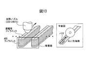
- Bipolar electrostatic chucks using two types of materials, conductive resin and insulating resin can be produced using the hot melt lamination method, but when trying to form a high-definition fiber, the shape targeted at the tip of the fiber is changed. It is often difficult to reproduce accurately (FIG. 13). Therefore, in a preferred embodiment of the present invention, as will be described in detail in Example 3, the heated glass plate smooth surface can be pressed to smooth the adsorbing portion of the device and improve the gripping performance. .
- Example 1 (Production of bipolar electrostatic chuck by photolithography technology) A beam assembly having a fine bristle structure was manufactured by wet etching using the processing process shown in FIG.
- the manufactured beam is made of SUS304, the shape is a tip area of 50 ⁇ m ⁇ 100 ⁇ m, the length is 8 mm, the mounting angle is 45 °, and the spring constant is 1.72 N / m.
- the number of beams is 12 and they are arranged at intervals of 400 ⁇ m.
- a scanning electron microscope (SEM) observation photograph of the fabricated beam assembly is shown in FIG. (a) shows the whole, and (b) shows the tip. Next, an insulating coating was applied to the manufactured beam assembly.
- the insulating agent used was 10 g of paraxylylene polymer “Parylene C”, and coating was performed by vacuum deposition.
- the origin of Parylene C was a dielectric strength of 200 V / mm and a relative dielectric constant of 3.15.
- Two pieces of the beam assembly subjected to insulation coating were bonded together. At this time, the position was adjusted by hand while observing with a microscope so that the tips were aligned, and the bonding was performed.
- the produced bipolar electrostatic chuck is shown in FIG. (a) shows the whole, and (b) shows the side.
- the direction in which the electrostatic chuck is pushed into the object is negative, the object surface is 0 point, and this is hereinafter referred to as displacement Z.
- the adsorption force is measured by reading the value of the electronic balance, and the interval for reading the value is 5 seconds.
- the resolution of the electronic balance is 0.1 ⁇ N.
- the automatic stage and electronic balance are installed in the Faraday cage so that they are not affected by the external electric field.
- FIG. 5 shows an experimental system.
- the adsorption force was estimated using the electrostatic field analysis of the finite element method analysis software “COMSOLMultiphysics” (registered trademark).
- the boundary condition is that the boundary of the beam assembly is ⁇ 200 V, and the boundary sufficiently separated.
- the object of analysis was glass with a relative dielectric constant of 4.1. The distance between the target surface and the beam tip was changed every 10 ⁇ m from 150 ⁇ m to 10 ⁇ m and every 1 ⁇ m from 10 ⁇ m to 1 ⁇ m.
- the adsorption force is obtained by dividing the Maxwell stress on the target surface into areas.
- F ⁇ ⁇ nTdS (1)
- n is a 1 ⁇ 3 unit row vector
- T is a Maxwell stress tensor (COMSOL AC / DC Module User's Guide, pp. 43-45).
- FIG. 7 shows the measured force curve and the analysis result by COMSOL.
- the maximum adsorption force measured was 63.6 ⁇ N, and the maximum adsorption force estimated by analysis was 360 ⁇ N.
- the fact that the suction force increases as the tip of the electrostatic chuck approaches the target surface is qualitatively consistent with the analysis results.
- quantitatively the measured maximum adsorption force decreased to about 1/6 of the analytical value.
- Possible causes of the decrease in the maximum adsorption force below the analytical value are misalignment of the beam tip and tip shape when two beam assemblies are bonded together.
- the electrostatic chuck produced this time was observed to have a deviation of 10 ⁇ m at the beam tip.
- FIG. 8 shows analysis results and measurement results in consideration of the tip shape. (a) shows the shift of the tip, (b) shows the shape of the tip, and (c) shows the force curve.
- E Young's modulus
- I the moment of inertia of the section
- l the beam length
- ⁇ the beam mounting angle.
- the beam assembly is manufactured by etching, a bipolar electrostatic chuck is manufactured using the beam assembly, and the adsorption performance is evaluated by comparing the adsorption force measurement experiment with the finite element method analysis by COMSOL. Went.
- the influence of the geometry of the beam tip on the attractive force is also shown.
- 3 layer integrated structure consisting of electrode layer-insulating layer-electrode layer can be manufactured as a single module by photolithography technology to eliminate the tip slip caused by manual work, and the area can be increased by stacking multiple modules. Can also be expected.
- it can be expected that the spring constant of the beam can be further reduced by changing the etching method and the beam size.
- Example 2 (Production of bipolar electrostatic chuck by 3D printer) As a 3D printer, a module was modeled using a MakerBot Replicator 2X of the FDM method (thermal melting lamination method). Specifications were as follows: nozzle diameter: 400 ⁇ m, minimum stacking pitch: 100 ⁇ m, positioning accuracy: XY direction: 11 ⁇ m, Z direction: 2.5 ⁇ m. In order to achieve stable modeling that ensures repeatability, the stacking pitch was 200 ⁇ m. Conductive resin filament (ESUN 3D FILAMENT CONDUCTIVE BLACK) was used as the conductor, and MakerBot's ABS resin was used as the insulator.
- nozzle diameter 400 ⁇ m
- minimum stacking pitch 100 ⁇ m
- positioning accuracy XY direction: 11 ⁇ m
- Z direction 2.5 ⁇ m.
- the stacking pitch was 200 ⁇ m.
- Conductive resin filament (ESUN 3D FILAMENT CONDUCTIVE BLACK) was used as the conductor
- MakerBot's ABS resin was used as the
- the thickness of the conductor was 0.4 mm, the thickness of the insulator was 0.8 mm, and a three-layer integrated structure having a thickness of 1.6 mm with the insulator sandwiched between the two conductors.
- the width of the suction surface was 1.2 mm, and the interval was 3.2 mm.
- the dimensions and appearance of the manufactured module are shown in FIGS. 9 (a) and 9 (b). (Performance evaluation of bipolar electrostatic chuck module)
- the applied voltage of positive electrode: 600V and negative electrode: -600V was applied to the electrodes of the manufactured bipolar electrostatic chuck module, and the lifting test of the object was performed by the three steps of contact, lifting and desorption.
- a polypropylene (PP) film (thickness 50 ⁇ m), tissue paper, and printing paper are cut into a rectangular shape of about 8 mm ⁇ 55 mm in accordance with the adsorption surface of the bipolar electrostatic chuck module and used as test pieces (mass is 5.9 mg each, 10.2 mg and 31.2 mg). All the test pieces were tested five times, and it was confirmed that all the test pieces can be securely grasped and detached (FIG. 10 (a): PP film, (b): tissue paper and (c ) Printing paper).
- FIG. 10A since it is difficult to recognize the PP film from the original image, processing such as contrast adjustment is performed.
- test piece was a slide glass (Matsunami Glass Industry Co., Ltd. S1111, size: 76 ⁇ 26 ⁇ 0.91 mm, mass: 4.59 g), and the force curve was measured in an experimental system in which the object was fixed.
- An outline of the experimental apparatus is shown in FIG. A stepwise displacement was given as a minimum of 0.01 mm every 20 seconds by an automatic linear stage, and the generated force at each position was measured with an analytical balance (Shimadzu AUW220D, resolution: 10 ⁇ gf, response time: 15 seconds).
- the applied voltage V 0, and the distance between the slide glass and the module is made sufficiently close, the inclination of the upper surface of the horizontally installed slide glass and the suction surface of the module are relatively compared, and the parallelism is visually adjusted.
- the applied voltages were positive electrode: 600V and negative electrode: -600V.
- the force curve obtained under the above experimental conditions is shown in FIG.
- the maximum adsorption force was 0.5495 gf.
- the maximum attraction force is greater in the separation process than in the approaching process, and hysteresis can be confirmed as a whole. This is thought to be due to compliance in the adsorption direction and electrostatic force due to the fine bristle structure.
- the abrupt decrease in adsorption force was confirmed as the beam tip of the module moved away from the slide glass. If compliance can be increased and hysteresis can be increased, more stable gripping can be achieved even in situations where disturbances occur during conveyance. In order to increase the compliance, it is conceivable to lengthen the beam, reduce the cross-sectional second moment of the beam, or use a material having a low bending elastic modulus.
- a bipolar electrostatic chuck module having a fine bristle structure is manufactured using a 3D printer, a lifting test on a film and paper, a force curve measurement on a glass plate, and a single-layer module is thin. It was confirmed that it sufficiently functions as a handling device for gripping soft materials. Furthermore, it is possible to grip a material having an arbitrary width by stacking modules. Further, by increasing the definition of the FDM 3D printer, it is possible to form a finer hair structure with a smaller scale, and to provide a bipolar electrostatic chuck module with a higher degree of freedom in terms of compliance.
- Example 3 Smoothing of the adsorption part using a heated flat plate
- a bipolar electrostatic chuck module (Fig. 15) made by laminating two single-layer modules with a fine bristle structure, created in the same way as in Example 2, using a 3D printer of the FDM method (heat melting lamination method)
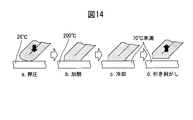
- the adsorption part was smoothed as follows (FIG. 14).
- a. A device suction surface that is visually aligned with the glass flat plate fixed on the hot plate is pressed 0.15 mm.
- the device adsorption part In the air (at 26 ° C atmosphere), the device adsorption part is heated via a glass plate (thickness 0.9 mm) by a hot plate (HHP-411V, maximum rated output 800 W) set at a heating temperature of 200 ° C. The smooth surface of the glass is transferred to the adsorption part softened by heat. c. It cools using a fan until the temperature of the surface of a glass flat plate falls to 70 degreeC, and a device adsorption
- the object is a polypropylene (PP) film cut into an 8 ⁇ 55 mm rectangle (mass: 59 mg, thickness: 50 ⁇ m) according to the size of the device gripping part.
- PP polypropylene
- the object is a slide glass (Matsunami Glass Kogyo Co., Ltd., S1111, size: 76 ⁇ 26 ⁇ 0.91 mm, mass: 4.59 g), and the force curve is shown in FIG. 11 in an experiment system in which the object is fixed. Measurement was performed using an apparatus. A stepwise displacement was given by 0.01 mm every 5 g by an automatic linear stage, and the generated force at each position was measured by an electronic balance (sartorius TE153S, reading limit: 0.001 g, response time: 2.5 seconds).
- the applied voltage V was set to 0, the parallelism was visually adjusted, the sample was moved closer to the slide glass at intervals of 5 ⁇ m, and the position when the value indicated by the electronic balance increased was used as the origin of the displacement Z.
- the applied voltage was positive electrode: 600V, negative electrode: -600V (electrode wiring:-, +, +,-(FIG. 15) from one side).
- Example 4 (Production of bipolar electrostatic chuck by photolithography technology)
- SOI Silicon on Insulator
- a bipolar electrostatic chuck module having a three-layer structure of conductor / dielectric / conductor was fabricated.
- Two Si layers become bipolar and SiO 2 insulates between the two .
- the area of the adsorption surface formed by the beam tip could be increased.
- the electrode portions of the modules that are in contact with each other were arranged to have the same pole.
- the SOI wafer was composed of three layers, an active layer (Si), an insulating layer (SiO 2 ), and a support layer (Si), and the thickness of each layer was 60 ⁇ m, 3 ⁇ m, and 435 ⁇ m, respectively.
- the shape of the beam having a fine bristle structure has a tip area of 200 ⁇ m ⁇ 498 ⁇ m, a length of 8 mm, and an attachment angle of 45 °.
- the number of beams is 12 and they are arranged at intervals of 300 ⁇ m.
- the manufacturing process of a bipolar electrostatic chuck having a beam assembly using dry etching is as follows.
- the entire wafer surface was coated with a Cr thin film.
- a photoresist (PR) negative type SU-8
- PR was spin-coated at 3000 rpm for 30 seconds to obtain a PR mask with a thickness of 38 ⁇ m.
- an exposure operation was performed to form a PR pattern on the wafer.
- the Cr thin film was etched according to the PR pattern.
- the active layer Si was shaved by a DRIE (Deep Reactive Ion Etching) method.
- Table 2 shows the cycle conditions of the etching gas SF 6 and the protective film gas C 4 F 8 used .
- FIG. 17 shows a schematic diagram when a bipolar electrostatic chuck module having a fine bristle structure of the present invention is used to grip, transport and peel a thin film having an arbitrary area such as a plastic film.
- a bipolar electrostatic chuck module having a fine bristle structure can be provided. Furthermore, according to the present invention, a bipolar electrostatic chuck can be modularized by integrally molding using a 3D printer or lithography technology, and the area of the fine bristle structure can be increased by stacking a plurality of modules. A bipolar electrostatic chuck module having a fine bristle structure capable of gripping a surface having an arbitrary area can be provided.
Landscapes
- Container, Conveyance, Adherence, Positioning, Of Wafer (AREA)
Abstract
本発明は、吸着面に微細毛構造を有し、プラスチックシートなどの薄膜誘電体に対応し得る双極型静電チャックを提供することを目的とする。吸着対象物を吸着するための静電チャック吸着面に微細毛構造を有し、吸着面の微細毛の先端部分には正極および負極間に絶縁層が配置され、正極と負極間に電圧を印加することにより静電力が生じ、静電チャック吸着面に吸着対象物が吸着されるように構成してなる双極型静電チャックモジュール。
Description
本発明は、双極型静電チャックモジュールおよびその製造方法に関する。
静電チャックは電圧印加時に対象物との間に働く静電力を利用し物体を把持,脱離するデバイスである。静電チャックは、誘電層と把持対象物の間に電位差を与え、発生した静電力により、把持対象物を吸着する機構であり、たとえば誘電体として絶縁材料を使用するクーロン力型がある。静電チャックはシリコンウェハーなど表面が平坦な物体の把持などに用いられているが、静電力は電極と対象物の間の距離に依存するため曲面など表面形状を有する物体に対しては吸着力が減少するという問題がある。
Radonらは、静電誘導ファイバーの集積構造によって吸着面に柔軟性を持つ静電チャックを開発した(非特許文献1)。しかし、その製作工程は,ファイバー1本1本を精密に配列する作業となるため,大面積化や電極の配線が困難であった.また、溶融紡糸法により製作されたファイバーは残留応力による変形のため先端が不揃いになる.またハンドリングが困難なことから集積が難しいという問題があった.そこで猿渡らは半導体製造に用いられるフォトリソグラフィ技術を用いて微細な導電性梁を配列し曲面対応デバイスを開発することを提案した(非特許文献2)。 しかしながら、これらの既存研究における静電チャックは単極型であることから誘電体へ対応できない難点がある。
R.Dhelikaet al., Smart Mater Struct., Vol.22pp.095010(1-9)2013
猿渡ら, 2015年度精密工学会春季大会学術講演会講演論文集, pp.805-8062015
本発明は、吸着面に微細毛構造を有し、プラスチックシートなどの薄膜誘電体に対応し得る双極型静電チャックを提供することを目的とする。さらに本発明は、2つの導電体間に絶縁体を挟む3層一体成形したものを1つの双極型静電チャックモジュールとし、このモジュールを積層することで吸着面である微細毛構造の大面積化を可能にするものである。
本発明は上記の問題を解決するために、以下の発明を提供するものである。
(1)吸着対象物を吸着するための静電チャック吸着面に微細毛構造を有し、吸着面の微細毛の先端部分には正極および負極間に絶縁層が配置され、正極と負極間に電圧を印加することにより静電力が生じ、静電チャック吸着面に吸着対象物が吸着されるように構成してなる双極型静電チャックモジュール。
(2)上記(1)に記載の複数の双極型静電チャックモジュールを積層してなる双極型静電チャックモジュール。
(3)静電チャック吸着面に吸着させる吸着対象物が布地、フィルムまたは紙である上記(1)または(2)に記載の双極型静電チャックモジュール。
(4)吸着対象物を吸着するための静電チャック吸着面に微細毛構造を有する双極型静電チャックモジュールを製造するに際して、導電体を用いてエッチング加工により、吸着面である先端部分に微細毛構造を有する梁集合体を製造し、得られた梁集合体に絶縁コーティングし、ついで絶縁コーティングされた2つの梁集合体を張り合わせて、正極および負極間に絶縁層を形成してなる双極型静電チャックモジュールを形成させることを特徴とする双極型静電チャックモジュールの製造方法。
(5)吸着対象物を吸着するための静電チャック吸着面に微細毛構造を有する双極型静電チャックモジュールを製造するに際して、導電体として導電性材料、絶縁体として絶縁性材料を用いて、3Dプリンターにより造形して2つの導電体である正極および負極間に絶縁体を形成し、吸着面に微細毛構造を有する双極型静電チャックモジュールを形成させることを特徴とする双極型静電チャックモジュールの製造方法。
(6)3Dプリンターが熱溶解積層法である上記(5)に記載の双極型静電チャックモジュールの製造方法。
(7)導電性材料が導電性樹脂フィラメントである上記(5)または(6)に記載の双極型静電チャックモジュールの製造方法。
(1)吸着対象物を吸着するための静電チャック吸着面に微細毛構造を有し、吸着面の微細毛の先端部分には正極および負極間に絶縁層が配置され、正極と負極間に電圧を印加することにより静電力が生じ、静電チャック吸着面に吸着対象物が吸着されるように構成してなる双極型静電チャックモジュール。
(2)上記(1)に記載の複数の双極型静電チャックモジュールを積層してなる双極型静電チャックモジュール。
(3)静電チャック吸着面に吸着させる吸着対象物が布地、フィルムまたは紙である上記(1)または(2)に記載の双極型静電チャックモジュール。
(4)吸着対象物を吸着するための静電チャック吸着面に微細毛構造を有する双極型静電チャックモジュールを製造するに際して、導電体を用いてエッチング加工により、吸着面である先端部分に微細毛構造を有する梁集合体を製造し、得られた梁集合体に絶縁コーティングし、ついで絶縁コーティングされた2つの梁集合体を張り合わせて、正極および負極間に絶縁層を形成してなる双極型静電チャックモジュールを形成させることを特徴とする双極型静電チャックモジュールの製造方法。
(5)吸着対象物を吸着するための静電チャック吸着面に微細毛構造を有する双極型静電チャックモジュールを製造するに際して、導電体として導電性材料、絶縁体として絶縁性材料を用いて、3Dプリンターにより造形して2つの導電体である正極および負極間に絶縁体を形成し、吸着面に微細毛構造を有する双極型静電チャックモジュールを形成させることを特徴とする双極型静電チャックモジュールの製造方法。
(6)3Dプリンターが熱溶解積層法である上記(5)に記載の双極型静電チャックモジュールの製造方法。
(7)導電性材料が導電性樹脂フィラメントである上記(5)または(6)に記載の双極型静電チャックモジュールの製造方法。
本発明によれば、微細毛構造を有する双極型静電チャックモジュールを提供し得る。さらに、本発明によれば、3Dプリンターやリソグラフィー技術を用いて双極型静電チャックを一体造形することでモジュール化し,複数のモジュールを積層することによって微細毛構造の大面積化を行うことができ、任意の面積を有する面を把持可能な微細毛構造を持つ双極型静電チャックモジュールを提供し得る。したがって、本発明によれば、各モジュールが微細毛を有しているため,静電吸着面に柔軟性を確保することが可能であり、従来円滑にハンドリングできない(吸着できてもうまく離脱できなかったり,吸着時に対象に損傷を与えたりする)ものを自由自在に吸着・離脱可能にすることができる。
本発明の静電チャックモジュールは、吸着対象物を吸着するための静電チャック吸着面に微細毛構造を有し、吸着面の微細毛の先端部分には正極および負極間に絶縁層が配置され、正極と負極間に電圧を印加することにより静電力が生じ、静電チャック吸着面に吸着対象物が吸着されるように構成してなる双極型静電チャックモジュールである。本発明の双極型静電チャックは、微細毛構造により吸着面に柔軟性を持つため、プラスチックフィルムや紙,布といった薄い軟材料に対して過剰なストレスを与えることのない面による繊細な把持・搬送・貼り付け(剥離動作)を可能にし,年々複雑化するウェアラブルデバイスにおける製造工程の自動化やフレキシブルエレクトロニクスといった柔軟媒体に対するハンドリング技術への適用に好適である。さらに本発明によれば、複数の双極型静電チャックモジュールを積層してなる双極型静電チャックモジュール積層体を提供し得る。すなわち、好適には3Dプリンターを用いて双極型静電チャックを一体造形することでモジュール化し,複数のモジュールを積層することによって微細毛構造の大面積化を行うことができる。本発明の静電チャックモジュールは、双極型であるために、通電しなくても誘電体材料を把持し得る。
図1に、双極型静電チャック単層モジュール1、および単層モジュールを積層することによって実現される大面積化された微細毛構造を有する双極型静電チャック(積層体)2の概念図を示す。図1において、3は正極、4は負極、5は絶縁層、6は微細毛構造を有する接触面(吸着面)を示す。
本発明の静電チャックモジュールにおいて、吸着対象物を吸着するための静電チャック吸着面の微細毛構造は、正極と負極、および絶縁層を構成する梁の先端部である吸着面に形成され、好適には、先端面積5μm×10μm~100μm×100μm程度、長さ5mm~300mm程度、間隔5μm~100μm、吸着面に対する取り付け角度30°~60°程度を有する梁集合体により形成されるが、これらに限定されるものではなく、吸着対象物の種類等により形状、寸法等が選択され得る。梁の本数も特に制限されないが、好適には、たとえば20~200本程度から選択される。微細毛構造は、好適には先端の形状がヘラ状である。
本発明の静電チャックモジュールは、微細毛構造を有するため、薄い軟材料に対してストレスを与えることのない面による繊細で、十分な把持力と容易な脱離機構を備える。すなわち、梁の先端が把持対象物に吸着(凝着)するので、把持力が吸着面に対して垂直方向に発生し、吸着面に対して回転してモーメントを与える方向に力を与えると吸着面に応力分布が発生し、高い応力状態が発生する部分から、把持対象物が脱離することになる。
本発明の好適な1実施態様において、本発明の微細毛構造を有する双極型静電チャックモジュールは、導電体を用いてエッチング加工により、吸着面である先端部分に微細毛構造を有する梁集合体を製造し、得られた梁集合体に絶縁コーティングし、ついで絶縁コーティングされた2つの梁集合体を張り合わせて、正極および負極間に絶縁層を形成してなる双極型静電チャックモジュールを形成させることにより製造される。
吸着面に微細毛構造を有する梁集合体を得るためにエッチング加工する導電体は、ステンレス鋼、アルミニウム、等の金属、ドープされたSiウエハ等の半導体、等が用いられる。
エッチング加工により先端部に微細毛構造を有する梁集合体が製造されるが、エッチングは、ウェットおよびドライのいずれも使用され得る。ウェットエッチングは、たとえば板状の導電体に所定のレジストマスクパターンを形成した後に、エッジング溶液に浸漬して行われる。エッチング溶液は、目的に応じて酸、アルカリ等の化学溶液から選定される。ドライエッチングは、真空容器内の放電プラズマ雰囲気下で行われ、たとえばプラズマ中で生成されたラジカル、ガスによる化学的エッチングが挙げられる。
微細毛構造を有る梁集合体は、前記のとおりである。
ついで、得られた梁集合体は、絶縁剤により絶縁コーティングされる。絶縁剤としては、パラキシリレンポリマー等の樹脂系、シリカ等のセラミックス系等が好適に使用される。コーティングは、蒸着法、浸漬法、スプレー法、ロールコーター法等によることができる。コーティング層の厚さは、得られる層の絶縁性、耐性等に応じて、適宜選定され得る。
ついで、絶縁コーティングされた2つの梁集合体を張り合わせて、2つの梁集合体、すなわち正極および負極間に絶縁層を形成させる。張り合わせは、位置合わせを行い、加圧、加熱して行い得る。
さらに、本発明の好適な1実施態様において、本発明の微細毛構造を有する双極型静電チャックモジュールは、導電体として導電性材料、絶縁体として絶縁性材料を用いて、3Dプリンターにより造形して2つの導電体間に絶縁体を形成し、吸着面に微細毛構造を有する双極型静電チャックモジュールを形成させることにより製造される。微細毛構造は、前記のとおりである。
3Dプリンターは、特に制限されず、溶融樹脂を押し出して積層する熱溶解積層法、液体樹脂を紫外線レーザーで硬化する光造形法、紫外線硬化性樹脂等をインクジェットヘッドを用いて微粒子状で噴射して積層面を印刷するインクジェット方式、樹脂または金属粉末材料にレーザーを照射し焼結させる粉末焼結法、等が採用され得る。
熱溶解積層法を用いる場合、導電性材料としては、導電性樹脂フィラメントが好適であり、グラフェン、カーボンナノファイバー、金属等の導電性フィラーが配合されたABS(アクリロニトリル・ブタジエン・スチレン)樹脂、PLA(ポリ乳酸)樹脂等の熱可塑性樹脂のフィラメントが挙げられる。絶縁性材料としては、ABS樹脂、等が挙げられる。熱溶融樹脂を溶解ヘッドから押し出して、成形テーブル上で1層ずつ積層して所定の立体形状が造形される。微細毛構造を有する双極型静電チャックモジュールの造形は、たとえば後述の実施例のように行われる。
光造形法を用いる場合、紫外線照射により硬化する光硬化性樹脂が用いられ、導電性樹脂としては、好適にはエポキシ樹脂が用いられ、絶縁性樹脂としては、各種のUV絶縁性インキ、等が挙げられる。造形ステージ上において1層目を形成後に、造形ステージは一層分下がり、2層目以降を繰り返して所定の造形物を得る。
熱溶解積層法を用いて導電性樹脂と絶縁性樹脂の2種の材料を用いた双極型静電チャックを作製し得るが、高精細なファイバーを造形しようとすると、ファイバー先端において狙った形状を正確に再現することが困難であることが多い(図13)。そこで、本発明の好適な1実施態様において、実施例3デ詳細に説明するように、加熱されたガラス板平滑面を押し当てることにより、デバイスの吸着部を平滑化し、把持性能を向上し得る。
熱溶解積層法を用いて導電性樹脂と絶縁性樹脂の2種の材料を用いた双極型静電チャックを作製し得るが、高精細なファイバーを造形しようとすると、ファイバー先端において狙った形状を正確に再現することが困難であることが多い(図13)。そこで、本発明の好適な1実施態様において、実施例3デ詳細に説明するように、加熱されたガラス板平滑面を押し当てることにより、デバイスの吸着部を平滑化し、把持性能を向上し得る。
以下、実施例により本発明をさらに詳細に説明する。
実施例1
(フォトリソグラフィ技術による双極型静電チャックの作製)
図2に示す加工プロセスを用いて、ウェットエッチング加工により微細毛構造を持つ梁集合体を製作した。製作した梁の材質はSUS304,形状は先端面積50μm×100μm,長さ8mm、取り付け角が45°、ばね定数は1.72N/mである。梁本数は12本で400μmの間隔で配列されている。製作した梁集合体の走査電子顕微鏡(SEM)観察写真を図3に示す。(a)は全体、(b)は先端を示す。
次に、製作した梁集合体に絶縁コーティングを行った。使用した絶縁剤はパラキシリレン系ポリマー「パリレンC」10gであり、真空蒸着でコーティングを行った。パリレンCの緒元は,絶縁耐力200V/mm,比誘電率3.15であった。絶縁コーティングを行った梁集合体を2枚張り合わせた。この時、先端が揃うよう顕微鏡で観察を行いながら手で位置を調整し張り合わせを行った。製作した双極型静電チャックを図4に示す。(a)は全体、(b)は側面を示す。
実施例1
(フォトリソグラフィ技術による双極型静電チャックの作製)
図2に示す加工プロセスを用いて、ウェットエッチング加工により微細毛構造を持つ梁集合体を製作した。製作した梁の材質はSUS304,形状は先端面積50μm×100μm,長さ8mm、取り付け角が45°、ばね定数は1.72N/mである。梁本数は12本で400μmの間隔で配列されている。製作した梁集合体の走査電子顕微鏡(SEM)観察写真を図3に示す。(a)は全体、(b)は先端を示す。
次に、製作した梁集合体に絶縁コーティングを行った。使用した絶縁剤はパラキシリレン系ポリマー「パリレンC」10gであり、真空蒸着でコーティングを行った。パリレンCの緒元は,絶縁耐力200V/mm,比誘電率3.15であった。絶縁コーティングを行った梁集合体を2枚張り合わせた。この時、先端が揃うよう顕微鏡で観察を行いながら手で位置を調整し張り合わせを行った。製作した双極型静電チャックを図4に示す。(a)は全体、(b)は側面を示す。
(吸着力測定実験)
製作した双極型静電チャックの吸着力測定実験を行った。測定対象は厚さ1mmの表面が平坦なスライドガラスを使用し、室温、大気中で測定した。
製作した双極型静電チャックの吸着力測定実験を行った。測定対象は厚さ1mmの表面が平坦なスライドガラスを使用し、室温、大気中で測定した。
静電チャックを対象に押し込む方向を負とし対象表面を0点とし,以降これを変位Zと呼ぶ。静電チャックに±200Vの電圧を印加した状態でステージをZ=150μmの位置から5秒ごとに1μmずつ引き下げていき、Z==-50μm押し込む。また、そこから同様の速度でZ=150μmまで引き上げる。吸着力は電子天秤の値を読み取ることにより測定を行い、値を読み取る間隔は5秒である。電子天秤の分解能は0.1μNである。自動ステージ,電子天秤はファラデーケージ内に設置されており、外部電場の影響を受けないようにしている。図5に実験系を示す。
(吸着力の有限要素法解析)
吸着性能の評価のため有限要素法解析ソフト「COMSOLMultiphysics」(登録商標)の静電場解析を用いて、吸着力の見積もりを行った。解析モデルは、梁が400μmの間隔で12本配列された梁集合体を2つ作成し,梁集合体間に誘電体を挟むものである(図6)。境界条件は梁集合体境界に±200V、十分離れた境界を接地している。解析対象は比誘電率4.1のガラスを使用した。また、対象表面と梁先端間の距離を150μmから10μmまでは10μmごとに,10μmから1μmまでは1μmごとに変化させた。吸着力は対象表面のマクスウェル応力を面積分することにより求める。
F=∫∂ΩnTdS(1)
この時、nは1×3の単位行ベクトル、Tはマクスウェル応力テンソルである(COMSOL AC/DC Module User’s Guide, pp.43-45)。
吸着性能の評価のため有限要素法解析ソフト「COMSOLMultiphysics」(登録商標)の静電場解析を用いて、吸着力の見積もりを行った。解析モデルは、梁が400μmの間隔で12本配列された梁集合体を2つ作成し,梁集合体間に誘電体を挟むものである(図6)。境界条件は梁集合体境界に±200V、十分離れた境界を接地している。解析対象は比誘電率4.1のガラスを使用した。また、対象表面と梁先端間の距離を150μmから10μmまでは10μmごとに,10μmから1μmまでは1μmごとに変化させた。吸着力は対象表面のマクスウェル応力を面積分することにより求める。
F=∫∂ΩnTdS(1)
この時、nは1×3の単位行ベクトル、Tはマクスウェル応力テンソルである(COMSOL AC/DC Module User’s Guide, pp.43-45)。
(結果)
測定したフォースカーブとCOMSOLによる解析結果を図7を示す。測定した最大吸着力は63.6μN、解析による最大吸着力の見積もりは360μNであった。静電チャック先端が対象表面に近づくと吸着力が大きくなるというところは定性的に解析結果と一致している。しかし定量的には測定した最大吸着力が解析値の1/6程度に低下した。最大吸着力が解析値よりも低下した原因として2枚の梁集合体を張り合わせた際の梁先端のミスアライメントと先端形状が考えられる。今回製作した静電チャックは梁先端に10μmのズレが観察された。また、梁1本の先端形状を観察すると平面が出ておらず、尖った形状をしていることが図8から分かる。図8に先端形状を考慮した解析結果と測定結果を示す。(a)は先端のシフト、(b)は先端の形状、(c)はフォースカーブを示す。
測定したフォースカーブとCOMSOLによる解析結果を図7を示す。測定した最大吸着力は63.6μN、解析による最大吸着力の見積もりは360μNであった。静電チャック先端が対象表面に近づくと吸着力が大きくなるというところは定性的に解析結果と一致している。しかし定量的には測定した最大吸着力が解析値の1/6程度に低下した。最大吸着力が解析値よりも低下した原因として2枚の梁集合体を張り合わせた際の梁先端のミスアライメントと先端形状が考えられる。今回製作した静電チャックは梁先端に10μmのズレが観察された。また、梁1本の先端形状を観察すると平面が出ておらず、尖った形状をしていることが図8から分かる。図8に先端形状を考慮した解析結果と測定結果を示す。(a)は先端のシフト、(b)は先端の形状、(c)はフォースカーブを示す。
先端の形状を考慮すると吸着力が低下する傾向がみられた。先端のズレは2枚の梁集合体を張り合わせる際に生じたものである。また梁先端に平面が出ていないのはエッチング加工の際に生じたと考えられる。しかし、静電チャック先端の形状を考慮しても最大吸着力が解析値の方が測定値よりも大きい。これは梁24本すべてが同時に測定対象表面に接触するのではなく、押し込み開始直後は対象を押込んでいる梁と静電力を発生させている梁があるため、測定対象に働く力が押込む力と静電力の和になる。この時、梁のばね定数が大きいと押込み力が静電力よりも大きくなってしまい測定対象に働く吸着力が低下してしまう。梁のばね定数は線形梁理論より求められる剛性
k=3EI/l3cosθ (2)
により決まる。この時、Eはヤング率,Iは断面二次モーメント,lは梁長さ,θは梁の取付け角である。これより、例えば梁長さを2倍にすることでばね定数は1/8まで小さくすることができ,吸着力の向上が期待できる。
k=3EI/l3cosθ (2)
により決まる。この時、Eはヤング率,Iは断面二次モーメント,lは梁長さ,θは梁の取付け角である。これより、例えば梁長さを2倍にすることでばね定数は1/8まで小さくすることができ,吸着力の向上が期待できる。
上記のように、ここではエッチング加工により梁集合体を製作し,それを用いて双極型静電チャックを作製し,吸着力測定実験とCOMSOLによる有限要素法解析を比較することにより吸着性能の評価を行った。また梁先端の幾何形状が吸着力に与える影響を示した。電極層-絶縁層-電極層からなる3層一体構造をフォトリソグラフィ技術により1モジュールとして製作することで手作業により生じた先端のすれなどを解消でき,また複数モジュールを積層することにより大面積化も期待できる。またエッチング方法や梁寸法を変えることにより梁のばね定数を今よりもさらに小さくすることが期待できる。
実施例2
(3Dプリンターによる双極型静電チャックの製作)
3Dプリンターとして,FDM方式(熱溶解積層法)のMakerBot Replicator 2Xを使用してモジュールの造形を行った。諸元はノズル径:400μm、最小積層ピッチ:100μm、位置決め精度はXY方向:11μm、Z方向:2.5μmであった。繰り返し性の確保される安定した造形を行うために,積層ピッチは200μmとした。導電体に導電性樹脂フィラメント(ESUN 3D FILAMENT CONDUCTIVE BLACK)、絶縁体にMakerBot純正のABS樹脂を使用した。導電体の厚さ0.4mm、絶縁体の厚さ0.8mmとし、2つの導電体間に絶縁体を挟む厚さ1.6mm の3層一体構造とした。吸着面の幅1.2mm、間隔3.2mmとした。製作したモジュールの寸法および外観を図9(a)および(b)に示す。
(双極型静電チャックモジュールの性能評価)
(3Dプリンターによる双極型静電チャックの製作)
3Dプリンターとして,FDM方式(熱溶解積層法)のMakerBot Replicator 2Xを使用してモジュールの造形を行った。諸元はノズル径:400μm、最小積層ピッチ:100μm、位置決め精度はXY方向:11μm、Z方向:2.5μmであった。繰り返し性の確保される安定した造形を行うために,積層ピッチは200μmとした。導電体に導電性樹脂フィラメント(ESUN 3D FILAMENT CONDUCTIVE BLACK)、絶縁体にMakerBot純正のABS樹脂を使用した。導電体の厚さ0.4mm、絶縁体の厚さ0.8mmとし、2つの導電体間に絶縁体を挟む厚さ1.6mm の3層一体構造とした。吸着面の幅1.2mm、間隔3.2mmとした。製作したモジュールの寸法および外観を図9(a)および(b)に示す。
(双極型静電チャックモジュールの性能評価)
製作した双極型静電チャックモジュールの電極に,正極:600V、負極:-600Vの印加電圧を与え,接触・持上げ・脱離の3行程による対象物の持上げ試験を行った。ポリプロピレン(PP)フィルム(厚さ50μm),ティッシュペーパーおよび印刷用紙を双極型静電チャックモジュールの吸着面に合わせて約8mm×55mmの長方形に切り取り試験片とした (質量は、それぞれ5.9mg、10.2mgおよび31.2mg)。全ての試験片において5回ずつ試験を行い,どの試験片も確実な把持・脱離が可能であることが確認された(図10(a):PPフィルム、(b):ティッシュペーパーおよび(c)印刷用紙)。図10(a)については,元画像からPPフィルムを認識することが困難なため,コントラスト調整などの加工を施した。
続いて,試験片をスライドグラス(松浪硝子工業株式会社S1111,サイズ:76× 26× 0.91mm、質量:4.59g)とし、対象物を固定した実験系でフォースカーブを測定した。実験装置の概要を図11に示す。自動直動ステージによりステップ状の変位を20秒毎に最小0.01mmとして与え,各位置での発生力を分析天秤(島津製作所AUW220D、分解能:10μgf,応答時間:15秒)により測定した。まず初めに印加電圧V=0として,スライドグラスとモジュールの間隔を十分に近づけ,水平に設置されたスライドグラスの上面とモジュールの吸着面の傾きを相対的に比較し目視で平行を調整した後,5μm間隔でスライドグラスに近づけ,分析天秤の示す値が増加したときの位置を変位Zの原点とした。変位Zは,モジュールからスライドグラスに向かう方向を正と定義し,開始点Z=-0.5mm から折り返し点Z=0.4mmの範囲で往復させて測定した。持ち上げ試験と同様に,印加電圧は正極:600V、負極:-600Vとした。
以上の実験条件により得られたフォースカーブを図12に示す。最大吸着力は0.5495gfであった。近づける過程に比べ引き離す過程の方が最大吸着力は大きくなり,全体としてもヒステリシスが確認できる。これは,微細毛構造による吸着方向のコンプライアンスと静電力が起因していると考えられる。図12のi、iiに示すように,モジュールの梁先端がスライドグラスから離れるとともに吸着力の急激な減少が確認できた。コンプライアンスを大きくし,ヒステリシスを大きくできれば、搬送時に外乱が生じるといった状況に対してもより安定した把持が可能になる。コンプライアンスを大きくするには,梁を長くする、梁の断面二次モーメントを小さくする、または曲げ弾性率の小さい材料を使用すること等が考えられる。
ここでは,上記のように、微細毛構造を持った双極型静電チャックモジュールを3Dプリンター用いて製作し、フィルムおよび紙に対する持上げ試験、ガラス板に対するフォースカーブの測定を行い、単層モジュールは薄い軟材料を把持するハンドリングデバイスとして十分機能することを確認した。さらに、モジュールの積層によって,任意の広さを持つ材料に対しても把持が行えるようにし得る。また,FDM方式3Dプリンターの高精細化によって,さらに小さなスケールの微細毛構造を造形することができ、コンプライアンスの点でより自由度の高い双極型静電チャックモジュールを提供し得る。
実施例3
(加熱平板を用いた吸着部の平滑化)
FDM方式(熱溶解積層法)の3Dプリンターを用いて実施例2と同様に作成された、微細毛構造を持った単層モジュールを2枚積層した双極型静電チャックモジュール(図15)を使用して、次のようにして吸着部の平滑化を行った(図14)。
a.ホットプレート上に固定されたガラス平板に、目視で平行を合わせたデバイス吸着面を0.15mm押し当てる。
b.大気中(26℃雰囲気)において、加熱温度200℃に設定されたホットプレート(HHP-411V、最大定格出力800W)により、ガラス平板(厚さ0.9mm)を介してデバイス吸着部を加熱し、熱により軟化した吸着部にガラスの平滑面を転写する。
c.ガラス平板表面の温度が70℃に低下するまでファンを用いて冷却し、デバイス吸着部を固化させる。
d.デバイスを上昇させ、ガラス平板に固着しているデバイス吸着部を引き剥がす。
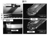
以上により平滑化されたデバイス吸着部の様子を図15に示す。
(加熱平板を用いた吸着部の平滑化)
FDM方式(熱溶解積層法)の3Dプリンターを用いて実施例2と同様に作成された、微細毛構造を持った単層モジュールを2枚積層した双極型静電チャックモジュール(図15)を使用して、次のようにして吸着部の平滑化を行った(図14)。
a.ホットプレート上に固定されたガラス平板に、目視で平行を合わせたデバイス吸着面を0.15mm押し当てる。
b.大気中(26℃雰囲気)において、加熱温度200℃に設定されたホットプレート(HHP-411V、最大定格出力800W)により、ガラス平板(厚さ0.9mm)を介してデバイス吸着部を加熱し、熱により軟化した吸着部にガラスの平滑面を転写する。
c.ガラス平板表面の温度が70℃に低下するまでファンを用いて冷却し、デバイス吸着部を固化させる。
d.デバイスを上昇させ、ガラス平板に固着しているデバイス吸着部を引き剥がす。
以上により平滑化されたデバイス吸着部の様子を図15に示す。
(把持性能改善の評価)
平滑化前後の双極型静電チャックの電極に、電圧を印加し、接触・持ち上げによる把持実験を行った。対象物は、デバイス把持部の大きさに合わせて8×55mmの長方形(質量:59mg、厚さ:50μm)に切り取られたポリプロピレン(PP)フィルムとする。
平滑化前後の双極型静電チャックの電極に、電圧を印加し、接触・持ち上げによる把持実験を行った。対象物は、デバイス把持部の大きさに合わせて8×55mmの長方形(質量:59mg、厚さ:50μm)に切り取られたポリプロピレン(PP)フィルムとする。
各印加電圧において5回の実験を行い、把持の成功率を得た(表1)。平滑化後の方が平滑化前に比べて、低い印加電圧でも把持可能であることから、平滑化によってデバイスの把持性能が高められていることがわかる。

続いて、対象物をスライドグラス(松浪硝子興業株式会社 S1111、サイズ:76×26×0.91mm、質量4.59g)とし、対象物が固定された実験系でフォースカーブを図11に示す実験装置を用いて測定した。自動直動ステージによりステップ状の変位を5g毎に0.01mmを与え,各位置での発生力を電子天秤(sartorius TE153S,読取限度:0.001g,応答時間:2.5秒)により測定した。初めに印加電圧V=0として,目視で平行を調整した後,5μm間隔でスライドグラスに近づけ,電子天秤の示す値が増加したときの位置を変位Zの原点とした。変位Zは,モジュールからスライドグラスに向かう方向を正と定義し,開始点Z=-1.5mm から折り返し点Z=0.4mmの範囲で往復させて測定した。印加電圧は正極:600V、負極:-600V(電極配線:片側から-、+、+、-(図15))とした。
以上により得られたフォースカーブ(図16(a):±600V)から接近と引き離しの間にヒステリシスが確認され、引き離し時に発生する最大吸着力が、平滑化前0.562gfから平滑化後2.446gfと、約4.35倍向上していることがわかる。一方、印加電圧0Vの条件におけるフォースカーブ(図16(b):0V)から、吸着力やヒステリシスがほとんど見られないため、吸着力の向上において固体間凝着力(分子間力)の影響は十分無視してよいといえる。以上のことから、本デバイスは、平滑化によりファイバー先端の吸着部と対象物の間で近接する面が増大し、吸着減少において支配的となる静電力がより効果的に働くように改善されていると考えられる。
実施例4
(フォトリソグラフィ技術による双極型静電チャックの作製)
2つのSi層の間に、SiO2が挟まれたSOI(Silicon on Insulator)ウェハーを用いることにより、導体/誘電体/導体の3層一体構造の双極型静電チャックモジュールを製作した。2つのSi層が双極になり、SiO2が両極の間を絶縁する。製作したモジュールを積層することで、梁先端が形成する吸着面の大面積化を図ることができた。互いに接するモジュールの電極部は同じ極となるように配置した。
(フォトリソグラフィ技術による双極型静電チャックの作製)
2つのSi層の間に、SiO2が挟まれたSOI(Silicon on Insulator)ウェハーを用いることにより、導体/誘電体/導体の3層一体構造の双極型静電チャックモジュールを製作した。2つのSi層が双極になり、SiO2が両極の間を絶縁する。製作したモジュールを積層することで、梁先端が形成する吸着面の大面積化を図ることができた。互いに接するモジュールの電極部は同じ極となるように配置した。
SOIウェハーは活性層(Si)、絶縁層(SiO2)および支持層(Si)の3層で構成し、各層の厚さはそれぞれ、60μm、3μm、435μmとした。微細毛構造を持つ梁の形状は、先端面積200μm×498μm、長さ8mm、取り付け角が45°である。梁本数は12本で300μmの間隔で配列されている。ドライエッチングを用いた梁集合体を有する双極型静電チャックの製作プロセスは下記のとおりである。
まず、ウェハー全面をCr薄膜でコートした。ついで、フォトレジスト(PR)(ネガティブ型SU-8)を塗布し、パターン通りに現像した。PRを3000rpmで30秒間、スピンコートし、厚さ38μmのPRマスクを得た。次に、露光作業を行い、ウェハー上にPRによるパターンを形成した。そして、Cr薄膜をPRパターン通りにエッチングした。以上のように、SOIウェハー表面の一部をCr薄膜とPRでマスキングしたことにより、マスクされていない領域のウェハーをエッチング作業で除去し得た。
Cr薄膜とPRによるエッチングマスクを製作した後に、活性層のSiをDRIE(Deep Reactive Ion Etching)法で削った。用いたエッチングガスSF6と保護膜ガスC4F8のサイクル条件は、表2の通りである。
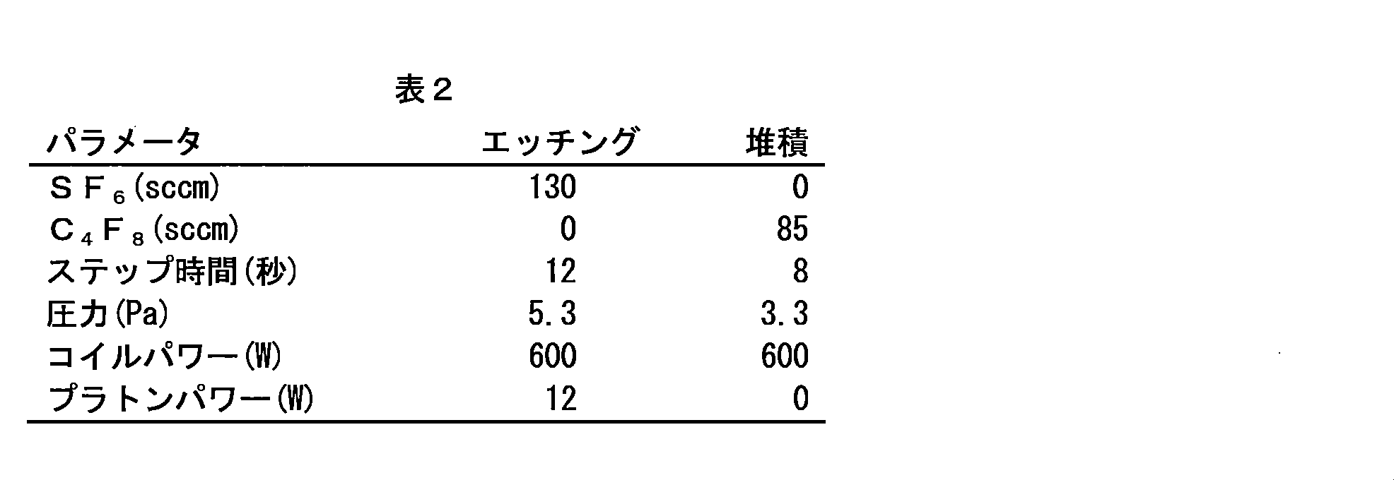
Cr薄膜とPRによるエッチングマスクを製作した後に、活性層のSiをDRIE(Deep Reactive Ion Etching)法で削った。用いたエッチングガスSF6と保護膜ガスC4F8のサイクル条件は、表2の通りである。
この条件において、平均1.8μm/分のエッチレートが得られ、活性層60μm厚さのSiを40分間、エッチングするとSiO2がウェハー全表面に現れた。ついで、このSiO2絶縁層をエッチング溶液としてフッ酸を用いて、ウェットエッチングした。ついで、残りの支持層SiをDRIE法でエッチングすることにより、梁集合体を有する双極型静電チャックを製作した。
図17に、本発明の微細毛構造を有する双極型静電チャックモジュールを用いて、プラスチックフィルム等の任意の面積を有する薄膜の把持、搬送および引き剥がしを行う場合の模式図を示す。
本発明によれば、微細毛構造を有する双極型静電チャックモジュールを提供し得る。さらに、本発明によれば、3Dプリンターやリソグラフィー技術を用いて双極型静電チャックを一体造形することでモジュール化し,複数のモジュールを積層することによって微細毛構造の大面積化を行うことができ、任意の面積を有する面を把持可能な微細毛構造を持つ双極型静電チャックモジュールを提供し得る。
Claims (7)
- 吸着対象物を吸着するための静電チャック吸着面に微細毛構造を有し、吸着面の微細毛の先端部分には正極および負極間に絶縁層が配置され、正極と負極間に電圧を印加することにより静電力が生じ、静電チャック吸着面に吸着対象物が吸着されるように構成してなる双極型静電チャックモジュール。
- 請求項1に記載の複数の双極型静電チャックモジュールを積層してなる双極型静電チャックモジュール。
- 静電チャック吸着面に吸着させる吸着対象物が布地、フィルムまたは紙である請求項1または2に記載の双極型静電チャックモジュール。
- 吸着対象物を吸着するための静電チャック吸着面に微細毛構造を有する双極型静電チャックモジュールを製造するに際して、導電体を用いてエッチング加工により、吸着面である先端部分に微細毛構造を有する梁集合体を製造し、得られた梁集合体に絶縁コーティングし、ついで絶縁コーティングされた2つの梁集合体を張り合わせて、正極および負極間に絶縁層を形成してなる双極型静電チャックモジュールを形成させることを特徴とする双極型静電チャックモジュールの製造方法。
- 吸着対象物を吸着するための静電チャック吸着面に微細毛構造を有する双極型静電チャックモジュールを製造するに際して、導電体として導電性材料、絶縁体として絶縁性材料を用いて、3Dプリンターにより造形して2つの導電体である正極および負極間に絶縁体を形成し、吸着面に微細毛構造を有する双極型静電チャックモジュールを形成させることを特徴とする双極型静電チャックモジュールの製造方法。
- 3Dプリンターが熱溶解積層法である請求項5に記載の双極型静電チャックモジュールの製造方法。
- 導電性材料が導電性樹脂フィラメントである請求項5または6に記載の双極型静電チャックモジュールの製造方法。
Priority Applications (1)
| Application Number | Priority Date | Filing Date | Title |
|---|---|---|---|
| JP2018503354A JP6846821B2 (ja) | 2016-02-29 | 2017-02-28 | 双極型静電チャックモジュールおよびその製造方法 |
Applications Claiming Priority (2)
| Application Number | Priority Date | Filing Date | Title |
|---|---|---|---|
| JP2016-038109 | 2016-02-29 | ||
| JP2016038109 | 2016-02-29 |
Publications (1)
| Publication Number | Publication Date |
|---|---|
| WO2017150574A1 true WO2017150574A1 (ja) | 2017-09-08 |
Family
ID=59744072
Family Applications (1)
| Application Number | Title | Priority Date | Filing Date |
|---|---|---|---|
| PCT/JP2017/007987 Ceased WO2017150574A1 (ja) | 2016-02-29 | 2017-02-28 | 双極型静電チャックモジュールおよびその製造方法 |
Country Status (2)
| Country | Link |
|---|---|
| JP (1) | JP6846821B2 (ja) |
| WO (1) | WO2017150574A1 (ja) |
Cited By (3)
| Publication number | Priority date | Publication date | Assignee | Title |
|---|---|---|---|---|
| US10730239B1 (en) | 2019-11-10 | 2020-08-04 | Yuri Glukhoy | 3D printing apparatus using a beam of an atmospheric pressure inductively coupled plasma generator |
| WO2024142605A1 (ja) * | 2022-12-27 | 2024-07-04 | 株式会社クリエイティブテクノロジー | 静電チャック、ロボット装置、及び物品把持装置 |
| JP7614687B1 (ja) | 2023-08-30 | 2025-01-16 | 国立大学法人東京科学大学 | 静電吸着デバイス、反り矯正方法、及び取付方法 |
Families Citing this family (1)
| Publication number | Priority date | Publication date | Assignee | Title |
|---|---|---|---|---|
| CN117837075A (zh) * | 2021-08-20 | 2024-04-05 | 国立大学法人东京工业大学 | 静电吸附设备以及静电吸附方法 |
Citations (1)
| Publication number | Priority date | Publication date | Assignee | Title |
|---|---|---|---|---|
| JP4961554B2 (ja) * | 2006-12-14 | 2012-06-27 | 国立大学法人東京工業大学 | 静電誘導吸着具及び静電誘導吸着方法 |
-
2017
- 2017-02-28 WO PCT/JP2017/007987 patent/WO2017150574A1/ja not_active Ceased
- 2017-02-28 JP JP2018503354A patent/JP6846821B2/ja active Active
Patent Citations (1)
| Publication number | Priority date | Publication date | Assignee | Title |
|---|---|---|---|---|
| JP4961554B2 (ja) * | 2006-12-14 | 2012-06-27 | 国立大学法人東京工業大学 | 静電誘導吸着具及び静電誘導吸着方法 |
Non-Patent Citations (2)
| Title |
|---|
| DHELIKA RADON ET AL.: "Electrostatic chuck consisting of polymeric electrostatic inductive fibers for handling of objects with rough surfaces", SMART MATERIALS AND STRUCTURES, vol. 22, no. 9, 5 August 2013 (2013-08-05), pages 95010, XP020250004 * |
| KEISUKE MAEZ ONO ET AL.: "Sokyoku-gata Seiden 1 y Yu den Fiber ni Okeru Denkyoku Danmen Keijo no 2-3 A Hasseiryoku eno Eikyo", 2012 NENDO THE JAPAN 4-7 SOCIETY FOR PRECISION ENGINEERING SHUNKI TAIKAI GAKUJUTSU KOENKAI KOEN RONBUNSHU, 1 March 2012 (2012-03-01), pages 701 - 702 * |
Cited By (4)
| Publication number | Priority date | Publication date | Assignee | Title |
|---|---|---|---|---|
| US10730239B1 (en) | 2019-11-10 | 2020-08-04 | Yuri Glukhoy | 3D printing apparatus using a beam of an atmospheric pressure inductively coupled plasma generator |
| WO2024142605A1 (ja) * | 2022-12-27 | 2024-07-04 | 株式会社クリエイティブテクノロジー | 静電チャック、ロボット装置、及び物品把持装置 |
| JP7614687B1 (ja) | 2023-08-30 | 2025-01-16 | 国立大学法人東京科学大学 | 静電吸着デバイス、反り矯正方法、及び取付方法 |
| WO2025047804A1 (ja) * | 2023-08-30 | 2025-03-06 | 国立大学法人東京工業大学 | 静電吸着デバイス、反り矯正方法、及び取付方法 |
Also Published As
| Publication number | Publication date |
|---|---|
| JP6846821B2 (ja) | 2021-03-24 |
| JPWO2017150574A1 (ja) | 2018-12-27 |
Similar Documents
| Publication | Publication Date | Title |
|---|---|---|
| WO2017150574A1 (ja) | 双極型静電チャックモジュールおよびその製造方法 | |
| JP6014587B2 (ja) | 高表面抵抗率の静電チャック | |
| CN101583436B (zh) | 用于挠性板件和基板接触的方法和系统 | |
| US10679884B2 (en) | Film electrode for electrostatic chuck | |
| WO2012005294A1 (ja) | 静電チャック装置及びその製造方法 | |
| KR20150014857A (ko) | 열 융착 전사를 이용한 유연 매립형 전극 필름의 제조 방법 | |
| JP6735656B2 (ja) | インプリント装置、インプリント方法及び物品の製造方法 | |
| CN112599592A (zh) | 高迁移率石墨烯在柔性衬底上的可规模放大、可印刷的图案化片材 | |
| TWI618116B (zh) | Imprinting device and method of manufacturing the same | |
| KR20080104947A (ko) | 패턴-천공된 마스크를 이용하는 하전입자의 집속 패터닝방법 및 이에 사용되는 마스크 | |
| KR101510801B1 (ko) | 정전흡착 장치용 미세섬모 구조물 | |
| JP2015151441A (ja) | 静電チャック用の接着シート及びその製造方法 | |
| US10777443B2 (en) | Imprint apparatus, imprinting method, and method for manufacturing article | |
| JP2017050355A (ja) | 電子デバイス及びその製造方法 | |
| KR20060024564A (ko) | 카본나노튜브의 정렬방법 및 이를 이용한 전계방출소자의제조방법 | |
| Taoka et al. | Development of Bipolar Electrostatic Chuck with a Beam-Array Assembly Fabricated by Lithography | |
| JP7295001B2 (ja) | 2d材料の大量組み立てのための方法及びシステム | |
| KR20130107081A (ko) | 나노 패터닝 장치, 이를 포함한 나노 패터닝 시스템 및 그 제어 방법 | |
| KR101350385B1 (ko) | 그래핀 레이어 형성장치 및 이에 사용되는 마이크로 피펫 | |
| JP2004066812A (ja) | 可撓性フィルムのラミネート方法およびラミネート装置並びに回路基板の製造方法 | |
| CN112864072A (zh) | 衬底的加工方法 | |
| JP3864612B2 (ja) | 微小構造体の製造方法および装置 | |
| TW202040833A (zh) | 用於轉移微型元件的方法 | |
| Yang et al. | The fabrication of integrated and three-layer SU-8 nozzles for electrohydrodynamic printing | |
| Wang et al. | Fabrication of Au micropatterns on vertical Si sidewalls using flexible PDMS shadow masks |
Legal Events
| Date | Code | Title | Description |
|---|---|---|---|
| ENP | Entry into the national phase |
Ref document number: 2018503354 Country of ref document: JP Kind code of ref document: A |
|
| NENP | Non-entry into the national phase |
Ref country code: DE |
|
| 121 | Ep: the epo has been informed by wipo that ep was designated in this application |
Ref document number: 17760038 Country of ref document: EP Kind code of ref document: A1 |
|
| 122 | Ep: pct application non-entry in european phase |
Ref document number: 17760038 Country of ref document: EP Kind code of ref document: A1 |