WO2017145299A1 - Electromagnetic wave detector - Google Patents
Electromagnetic wave detector Download PDFInfo
- Publication number
- WO2017145299A1 WO2017145299A1 PCT/JP2016/055485 JP2016055485W WO2017145299A1 WO 2017145299 A1 WO2017145299 A1 WO 2017145299A1 JP 2016055485 W JP2016055485 W JP 2016055485W WO 2017145299 A1 WO2017145299 A1 WO 2017145299A1
- Authority
- WO
- WIPO (PCT)
- Prior art keywords
- layer
- electromagnetic wave
- contact
- wave detector
- graphene
- Prior art date
Links
- OKTJSMMVPCPJKN-UHFFFAOYSA-N Carbon Chemical compound [C] OKTJSMMVPCPJKN-UHFFFAOYSA-N 0.000 claims abstract description 238
- 229910021389 graphene Inorganic materials 0.000 claims abstract description 237
- 239000000463 material Substances 0.000 claims abstract description 92
- 239000000758 substrate Substances 0.000 claims abstract description 33
- 238000006243 chemical reaction Methods 0.000 claims abstract description 16
- 230000000737 periodic effect Effects 0.000 claims description 30
- 229910052723 transition metal Inorganic materials 0.000 claims description 10
- 150000003624 transition metals Chemical class 0.000 claims description 10
- OAICVXFJPJFONN-UHFFFAOYSA-N Phosphorus Chemical compound [P] OAICVXFJPJFONN-UHFFFAOYSA-N 0.000 claims description 9
- 125000002887 hydroxy group Chemical group [H]O* 0.000 claims description 6
- 239000000126 substance Substances 0.000 claims description 6
- 125000003178 carboxy group Chemical group [H]OC(*)=O 0.000 claims description 5
- 238000006479 redox reaction Methods 0.000 claims description 4
- 229910010272 inorganic material Inorganic materials 0.000 claims description 3
- 239000011147 inorganic material Substances 0.000 claims description 3
- 229920003986 novolac Polymers 0.000 claims description 3
- 239000003504 photosensitizing agent Substances 0.000 claims description 3
- 239000002861 polymer material Substances 0.000 claims description 2
- 239000002131 composite material Substances 0.000 claims 1
- 239000010410 layer Substances 0.000 description 383
- 238000001514 detection method Methods 0.000 description 28
- 239000010408 film Substances 0.000 description 22
- 230000035945 sensitivity Effects 0.000 description 22
- 238000000034 method Methods 0.000 description 18
- 230000008569 process Effects 0.000 description 16
- 229910052751 metal Inorganic materials 0.000 description 13
- 239000002184 metal Substances 0.000 description 13
- 229920002120 photoresistant polymer Polymers 0.000 description 10
- 230000000694 effects Effects 0.000 description 9
- 230000010287 polarization Effects 0.000 description 9
- 125000006575 electron-withdrawing group Chemical group 0.000 description 8
- 230000001681 protective effect Effects 0.000 description 8
- 239000004065 semiconductor Substances 0.000 description 8
- XUIMIQQOPSSXEZ-UHFFFAOYSA-N Silicon Chemical compound [Si] XUIMIQQOPSSXEZ-UHFFFAOYSA-N 0.000 description 7
- 229910052710 silicon Inorganic materials 0.000 description 7
- 239000010703 silicon Substances 0.000 description 7
- 230000008859 change Effects 0.000 description 6
- 230000003287 optical effect Effects 0.000 description 6
- 238000002198 surface plasmon resonance spectroscopy Methods 0.000 description 6
- 238000005229 chemical vapour deposition Methods 0.000 description 5
- 229910052581 Si3N4 Inorganic materials 0.000 description 4
- 229910004298 SiO 2 Inorganic materials 0.000 description 4
- 239000000969 carrier Substances 0.000 description 4
- 229910052804 chromium Inorganic materials 0.000 description 4
- 229910052737 gold Inorganic materials 0.000 description 4
- 239000010931 gold Substances 0.000 description 4
- 238000004519 manufacturing process Methods 0.000 description 4
- 239000000203 mixture Substances 0.000 description 4
- 238000000206 photolithography Methods 0.000 description 4
- 238000012545 processing Methods 0.000 description 4
- HQVNEWCFYHHQES-UHFFFAOYSA-N silicon nitride Chemical compound N12[Si]34N5[Si]62N3[Si]51N64 HQVNEWCFYHHQES-UHFFFAOYSA-N 0.000 description 4
- 239000002356 single layer Substances 0.000 description 4
- VYPSYNLAJGMNEJ-UHFFFAOYSA-N Silicium dioxide Chemical compound O=[Si]=O VYPSYNLAJGMNEJ-UHFFFAOYSA-N 0.000 description 3
- 229910052782 aluminium Inorganic materials 0.000 description 3
- 230000015572 biosynthetic process Effects 0.000 description 3
- 230000007423 decrease Effects 0.000 description 3
- 238000010586 diagram Methods 0.000 description 3
- 230000005684 electric field Effects 0.000 description 3
- 238000000605 extraction Methods 0.000 description 3
- 238000009413 insulation Methods 0.000 description 3
- 239000012212 insulator Substances 0.000 description 3
- 229910044991 metal oxide Inorganic materials 0.000 description 3
- 150000004706 metal oxides Chemical class 0.000 description 3
- 229910052814 silicon oxide Inorganic materials 0.000 description 3
- 229910052709 silver Inorganic materials 0.000 description 3
- WGTYBPLFGIVFAS-UHFFFAOYSA-M tetramethylammonium hydroxide Chemical compound [OH-].C[N+](C)(C)C WGTYBPLFGIVFAS-UHFFFAOYSA-M 0.000 description 3
- PZNSFCLAULLKQX-UHFFFAOYSA-N Boron nitride Chemical compound N#B PZNSFCLAULLKQX-UHFFFAOYSA-N 0.000 description 2
- 229910052799 carbon Inorganic materials 0.000 description 2
- 229910052802 copper Inorganic materials 0.000 description 2
- 238000011161 development Methods 0.000 description 2
- 238000003384 imaging method Methods 0.000 description 2
- 238000005259 measurement Methods 0.000 description 2
- 150000002739 metals Chemical class 0.000 description 2
- 239000002074 nanoribbon Substances 0.000 description 2
- 229910052759 nickel Inorganic materials 0.000 description 2
- PXHVJJICTQNCMI-UHFFFAOYSA-N nickel Substances [Ni] PXHVJJICTQNCMI-UHFFFAOYSA-N 0.000 description 2
- TWNQGVIAIRXVLR-UHFFFAOYSA-N oxo(oxoalumanyloxy)alumane Chemical compound O=[Al]O[Al]=O TWNQGVIAIRXVLR-UHFFFAOYSA-N 0.000 description 2
- 230000000149 penetrating effect Effects 0.000 description 2
- 230000009467 reduction Effects 0.000 description 2
- 238000006722 reduction reaction Methods 0.000 description 2
- 230000004044 response Effects 0.000 description 2
- 238000004544 sputter deposition Methods 0.000 description 2
- 238000012546 transfer Methods 0.000 description 2
- 239000013598 vector Substances 0.000 description 2
- 229910018072 Al 2 O 3 Inorganic materials 0.000 description 1
- 229910052582 BN Inorganic materials 0.000 description 1
- LFQSCWFLJHTTHZ-UHFFFAOYSA-N Ethanol Chemical compound CCO LFQSCWFLJHTTHZ-UHFFFAOYSA-N 0.000 description 1
- 238000010521 absorption reaction Methods 0.000 description 1
- 125000000217 alkyl group Chemical group 0.000 description 1
- 125000003277 amino group Chemical group 0.000 description 1
- 239000012298 atmosphere Substances 0.000 description 1
- QVGXLLKOCUKJST-UHFFFAOYSA-N atomic oxygen Chemical compound [O] QVGXLLKOCUKJST-UHFFFAOYSA-N 0.000 description 1
- 150000001721 carbon Chemical group 0.000 description 1
- 125000004432 carbon atom Chemical group C* 0.000 description 1
- 125000002915 carbonyl group Chemical group [*:2]C([*:1])=O 0.000 description 1
- 239000003795 chemical substances by application Substances 0.000 description 1
- 238000000576 coating method Methods 0.000 description 1
- 239000013078 crystal Substances 0.000 description 1
- 230000003247 decreasing effect Effects 0.000 description 1
- 238000000151 deposition Methods 0.000 description 1
- 230000008030 elimination Effects 0.000 description 1
- 238000003379 elimination reaction Methods 0.000 description 1
- 238000005530 etching Methods 0.000 description 1
- 239000007789 gas Substances 0.000 description 1
- PCHJSUWPFVWCPO-UHFFFAOYSA-N gold Chemical compound [Au] PCHJSUWPFVWCPO-UHFFFAOYSA-N 0.000 description 1
- 229910052736 halogen Inorganic materials 0.000 description 1
- 150000002367 halogens Chemical class 0.000 description 1
- BHEPBYXIRTUNPN-UHFFFAOYSA-N hydridophosphorus(.) (triplet) Chemical compound [PH] BHEPBYXIRTUNPN-UHFFFAOYSA-N 0.000 description 1
- 230000003993 interaction Effects 0.000 description 1
- 230000001678 irradiating effect Effects 0.000 description 1
- 230000031700 light absorption Effects 0.000 description 1
- 239000007788 liquid Substances 0.000 description 1
- 239000011159 matrix material Substances 0.000 description 1
- 229910052752 metalloid Inorganic materials 0.000 description 1
- 150000002738 metalloids Chemical class 0.000 description 1
- 230000007935 neutral effect Effects 0.000 description 1
- 229910000480 nickel oxide Inorganic materials 0.000 description 1
- 150000002825 nitriles Chemical class 0.000 description 1
- 239000005416 organic matter Substances 0.000 description 1
- 230000001590 oxidative effect Effects 0.000 description 1
- GNRSAWUEBMWBQH-UHFFFAOYSA-N oxonickel Chemical compound [Ni]=O GNRSAWUEBMWBQH-UHFFFAOYSA-N 0.000 description 1
- 229910052760 oxygen Inorganic materials 0.000 description 1
- 239000001301 oxygen Substances 0.000 description 1
- 230000002093 peripheral effect Effects 0.000 description 1
- 229920000642 polymer Polymers 0.000 description 1
- 239000011241 protective layer Substances 0.000 description 1
- 230000006798 recombination Effects 0.000 description 1
- 238000005215 recombination Methods 0.000 description 1
- 229920005989 resin Polymers 0.000 description 1
- 239000011347 resin Substances 0.000 description 1
- 238000010187 selection method Methods 0.000 description 1
- 239000007787 solid Substances 0.000 description 1
- 239000010409 thin film Substances 0.000 description 1
- 238000007740 vapor deposition Methods 0.000 description 1
Images


Classifications
-
- H—ELECTRICITY
- H01—ELECTRIC ELEMENTS
- H01L—SEMICONDUCTOR DEVICES NOT COVERED BY CLASS H10
- H01L31/00—Semiconductor devices sensitive to infrared radiation, light, electromagnetic radiation of shorter wavelength or corpuscular radiation and specially adapted either for the conversion of the energy of such radiation into electrical energy or for the control of electrical energy by such radiation; Processes or apparatus specially adapted for the manufacture or treatment thereof or of parts thereof; Details thereof
- H01L31/0248—Semiconductor devices sensitive to infrared radiation, light, electromagnetic radiation of shorter wavelength or corpuscular radiation and specially adapted either for the conversion of the energy of such radiation into electrical energy or for the control of electrical energy by such radiation; Processes or apparatus specially adapted for the manufacture or treatment thereof or of parts thereof; Details thereof characterised by their semiconductor bodies
- H01L31/0256—Semiconductor devices sensitive to infrared radiation, light, electromagnetic radiation of shorter wavelength or corpuscular radiation and specially adapted either for the conversion of the energy of such radiation into electrical energy or for the control of electrical energy by such radiation; Processes or apparatus specially adapted for the manufacture or treatment thereof or of parts thereof; Details thereof characterised by their semiconductor bodies characterised by the material
- H01L31/0264—Inorganic materials
- H01L31/028—Inorganic materials including, apart from doping material or other impurities, only elements of Group IV of the Periodic Table
-
- H—ELECTRICITY
- H01—ELECTRIC ELEMENTS
- H01L—SEMICONDUCTOR DEVICES NOT COVERED BY CLASS H10
- H01L27/00—Devices consisting of a plurality of semiconductor or other solid-state components formed in or on a common substrate
- H01L27/14—Devices consisting of a plurality of semiconductor or other solid-state components formed in or on a common substrate including semiconductor components sensitive to infrared radiation, light, electromagnetic radiation of shorter wavelength or corpuscular radiation and specially adapted either for the conversion of the energy of such radiation into electrical energy or for the control of electrical energy by such radiation
- H01L27/144—Devices controlled by radiation
- H01L27/1443—Devices controlled by radiation with at least one potential jump or surface barrier
-
- H—ELECTRICITY
- H01—ELECTRIC ELEMENTS
- H01L—SEMICONDUCTOR DEVICES NOT COVERED BY CLASS H10
- H01L27/00—Devices consisting of a plurality of semiconductor or other solid-state components formed in or on a common substrate
- H01L27/14—Devices consisting of a plurality of semiconductor or other solid-state components formed in or on a common substrate including semiconductor components sensitive to infrared radiation, light, electromagnetic radiation of shorter wavelength or corpuscular radiation and specially adapted either for the conversion of the energy of such radiation into electrical energy or for the control of electrical energy by such radiation
- H01L27/144—Devices controlled by radiation
- H01L27/1446—Devices controlled by radiation in a repetitive configuration
-
- H—ELECTRICITY
- H01—ELECTRIC ELEMENTS
- H01L—SEMICONDUCTOR DEVICES NOT COVERED BY CLASS H10
- H01L31/00—Semiconductor devices sensitive to infrared radiation, light, electromagnetic radiation of shorter wavelength or corpuscular radiation and specially adapted either for the conversion of the energy of such radiation into electrical energy or for the control of electrical energy by such radiation; Processes or apparatus specially adapted for the manufacture or treatment thereof or of parts thereof; Details thereof
- H01L31/02—Details
- H01L31/0216—Coatings
- H01L31/02161—Coatings for devices characterised by at least one potential jump barrier or surface barrier
-
- H—ELECTRICITY
- H01—ELECTRIC ELEMENTS
- H01L—SEMICONDUCTOR DEVICES NOT COVERED BY CLASS H10
- H01L31/00—Semiconductor devices sensitive to infrared radiation, light, electromagnetic radiation of shorter wavelength or corpuscular radiation and specially adapted either for the conversion of the energy of such radiation into electrical energy or for the control of electrical energy by such radiation; Processes or apparatus specially adapted for the manufacture or treatment thereof or of parts thereof; Details thereof
- H01L31/02—Details
- H01L31/0224—Electrodes
- H01L31/022408—Electrodes for devices characterised by at least one potential jump barrier or surface barrier
-
- H—ELECTRICITY
- H01—ELECTRIC ELEMENTS
- H01L—SEMICONDUCTOR DEVICES NOT COVERED BY CLASS H10
- H01L31/00—Semiconductor devices sensitive to infrared radiation, light, electromagnetic radiation of shorter wavelength or corpuscular radiation and specially adapted either for the conversion of the energy of such radiation into electrical energy or for the control of electrical energy by such radiation; Processes or apparatus specially adapted for the manufacture or treatment thereof or of parts thereof; Details thereof
- H01L31/02—Details
- H01L31/0232—Optical elements or arrangements associated with the device
-
- H—ELECTRICITY
- H01—ELECTRIC ELEMENTS
- H01L—SEMICONDUCTOR DEVICES NOT COVERED BY CLASS H10
- H01L31/00—Semiconductor devices sensitive to infrared radiation, light, electromagnetic radiation of shorter wavelength or corpuscular radiation and specially adapted either for the conversion of the energy of such radiation into electrical energy or for the control of electrical energy by such radiation; Processes or apparatus specially adapted for the manufacture or treatment thereof or of parts thereof; Details thereof
- H01L31/02—Details
- H01L31/0236—Special surface textures
- H01L31/02366—Special surface textures of the substrate or of a layer on the substrate, e.g. textured ITO/glass substrate or superstrate, textured polymer layer on glass substrate
-
- H—ELECTRICITY
- H01—ELECTRIC ELEMENTS
- H01L—SEMICONDUCTOR DEVICES NOT COVERED BY CLASS H10
- H01L31/00—Semiconductor devices sensitive to infrared radiation, light, electromagnetic radiation of shorter wavelength or corpuscular radiation and specially adapted either for the conversion of the energy of such radiation into electrical energy or for the control of electrical energy by such radiation; Processes or apparatus specially adapted for the manufacture or treatment thereof or of parts thereof; Details thereof
- H01L31/0248—Semiconductor devices sensitive to infrared radiation, light, electromagnetic radiation of shorter wavelength or corpuscular radiation and specially adapted either for the conversion of the energy of such radiation into electrical energy or for the control of electrical energy by such radiation; Processes or apparatus specially adapted for the manufacture or treatment thereof or of parts thereof; Details thereof characterised by their semiconductor bodies
- H01L31/0256—Semiconductor devices sensitive to infrared radiation, light, electromagnetic radiation of shorter wavelength or corpuscular radiation and specially adapted either for the conversion of the energy of such radiation into electrical energy or for the control of electrical energy by such radiation; Processes or apparatus specially adapted for the manufacture or treatment thereof or of parts thereof; Details thereof characterised by their semiconductor bodies characterised by the material
- H01L31/0264—Inorganic materials
- H01L31/028—Inorganic materials including, apart from doping material or other impurities, only elements of Group IV of the Periodic Table
- H01L31/0288—Inorganic materials including, apart from doping material or other impurities, only elements of Group IV of the Periodic Table characterised by the doping material
-
- H—ELECTRICITY
- H01—ELECTRIC ELEMENTS
- H01L—SEMICONDUCTOR DEVICES NOT COVERED BY CLASS H10
- H01L31/00—Semiconductor devices sensitive to infrared radiation, light, electromagnetic radiation of shorter wavelength or corpuscular radiation and specially adapted either for the conversion of the energy of such radiation into electrical energy or for the control of electrical energy by such radiation; Processes or apparatus specially adapted for the manufacture or treatment thereof or of parts thereof; Details thereof
- H01L31/0248—Semiconductor devices sensitive to infrared radiation, light, electromagnetic radiation of shorter wavelength or corpuscular radiation and specially adapted either for the conversion of the energy of such radiation into electrical energy or for the control of electrical energy by such radiation; Processes or apparatus specially adapted for the manufacture or treatment thereof or of parts thereof; Details thereof characterised by their semiconductor bodies
- H01L31/0352—Semiconductor devices sensitive to infrared radiation, light, electromagnetic radiation of shorter wavelength or corpuscular radiation and specially adapted either for the conversion of the energy of such radiation into electrical energy or for the control of electrical energy by such radiation; Processes or apparatus specially adapted for the manufacture or treatment thereof or of parts thereof; Details thereof characterised by their semiconductor bodies characterised by their shape or by the shapes, relative sizes or disposition of the semiconductor regions
- H01L31/035209—Semiconductor devices sensitive to infrared radiation, light, electromagnetic radiation of shorter wavelength or corpuscular radiation and specially adapted either for the conversion of the energy of such radiation into electrical energy or for the control of electrical energy by such radiation; Processes or apparatus specially adapted for the manufacture or treatment thereof or of parts thereof; Details thereof characterised by their semiconductor bodies characterised by their shape or by the shapes, relative sizes or disposition of the semiconductor regions comprising a quantum structures
-
- H—ELECTRICITY
- H01—ELECTRIC ELEMENTS
- H01L—SEMICONDUCTOR DEVICES NOT COVERED BY CLASS H10
- H01L31/00—Semiconductor devices sensitive to infrared radiation, light, electromagnetic radiation of shorter wavelength or corpuscular radiation and specially adapted either for the conversion of the energy of such radiation into electrical energy or for the control of electrical energy by such radiation; Processes or apparatus specially adapted for the manufacture or treatment thereof or of parts thereof; Details thereof
- H01L31/08—Semiconductor devices sensitive to infrared radiation, light, electromagnetic radiation of shorter wavelength or corpuscular radiation and specially adapted either for the conversion of the energy of such radiation into electrical energy or for the control of electrical energy by such radiation; Processes or apparatus specially adapted for the manufacture or treatment thereof or of parts thereof; Details thereof in which radiation controls flow of current through the device, e.g. photoresistors
- H01L31/10—Semiconductor devices sensitive to infrared radiation, light, electromagnetic radiation of shorter wavelength or corpuscular radiation and specially adapted either for the conversion of the energy of such radiation into electrical energy or for the control of electrical energy by such radiation; Processes or apparatus specially adapted for the manufacture or treatment thereof or of parts thereof; Details thereof in which radiation controls flow of current through the device, e.g. photoresistors characterised by potential barriers, e.g. phototransistors
- H01L31/101—Devices sensitive to infrared, visible or ultraviolet radiation
- H01L31/102—Devices sensitive to infrared, visible or ultraviolet radiation characterised by only one potential barrier
- H01L31/103—Devices sensitive to infrared, visible or ultraviolet radiation characterised by only one potential barrier the potential barrier being of the PN homojunction type
-
- H—ELECTRICITY
- H01—ELECTRIC ELEMENTS
- H01L—SEMICONDUCTOR DEVICES NOT COVERED BY CLASS H10
- H01L31/00—Semiconductor devices sensitive to infrared radiation, light, electromagnetic radiation of shorter wavelength or corpuscular radiation and specially adapted either for the conversion of the energy of such radiation into electrical energy or for the control of electrical energy by such radiation; Processes or apparatus specially adapted for the manufacture or treatment thereof or of parts thereof; Details thereof
- H01L31/08—Semiconductor devices sensitive to infrared radiation, light, electromagnetic radiation of shorter wavelength or corpuscular radiation and specially adapted either for the conversion of the energy of such radiation into electrical energy or for the control of electrical energy by such radiation; Processes or apparatus specially adapted for the manufacture or treatment thereof or of parts thereof; Details thereof in which radiation controls flow of current through the device, e.g. photoresistors
- H01L31/10—Semiconductor devices sensitive to infrared radiation, light, electromagnetic radiation of shorter wavelength or corpuscular radiation and specially adapted either for the conversion of the energy of such radiation into electrical energy or for the control of electrical energy by such radiation; Processes or apparatus specially adapted for the manufacture or treatment thereof or of parts thereof; Details thereof in which radiation controls flow of current through the device, e.g. photoresistors characterised by potential barriers, e.g. phototransistors
- H01L31/101—Devices sensitive to infrared, visible or ultraviolet radiation
- H01L31/112—Devices sensitive to infrared, visible or ultraviolet radiation characterised by field-effect operation, e.g. junction field-effect phototransistor
-
- H—ELECTRICITY
- H01—ELECTRIC ELEMENTS
- H01L—SEMICONDUCTOR DEVICES NOT COVERED BY CLASS H10
- H01L31/00—Semiconductor devices sensitive to infrared radiation, light, electromagnetic radiation of shorter wavelength or corpuscular radiation and specially adapted either for the conversion of the energy of such radiation into electrical energy or for the control of electrical energy by such radiation; Processes or apparatus specially adapted for the manufacture or treatment thereof or of parts thereof; Details thereof
- H01L31/18—Processes or apparatus specially adapted for the manufacture or treatment of these devices or of parts thereof
- H01L31/1804—Processes or apparatus specially adapted for the manufacture or treatment of these devices or of parts thereof comprising only elements of Group IV of the Periodic Table
-
- Y—GENERAL TAGGING OF NEW TECHNOLOGICAL DEVELOPMENTS; GENERAL TAGGING OF CROSS-SECTIONAL TECHNOLOGIES SPANNING OVER SEVERAL SECTIONS OF THE IPC; TECHNICAL SUBJECTS COVERED BY FORMER USPC CROSS-REFERENCE ART COLLECTIONS [XRACs] AND DIGESTS
- Y02—TECHNOLOGIES OR APPLICATIONS FOR MITIGATION OR ADAPTATION AGAINST CLIMATE CHANGE
- Y02E—REDUCTION OF GREENHOUSE GAS [GHG] EMISSIONS, RELATED TO ENERGY GENERATION, TRANSMISSION OR DISTRIBUTION
- Y02E10/00—Energy generation through renewable energy sources
- Y02E10/50—Photovoltaic [PV] energy
- Y02E10/547—Monocrystalline silicon PV cells
-
- Y—GENERAL TAGGING OF NEW TECHNOLOGICAL DEVELOPMENTS; GENERAL TAGGING OF CROSS-SECTIONAL TECHNOLOGIES SPANNING OVER SEVERAL SECTIONS OF THE IPC; TECHNICAL SUBJECTS COVERED BY FORMER USPC CROSS-REFERENCE ART COLLECTIONS [XRACs] AND DIGESTS
- Y02—TECHNOLOGIES OR APPLICATIONS FOR MITIGATION OR ADAPTATION AGAINST CLIMATE CHANGE
- Y02P—CLIMATE CHANGE MITIGATION TECHNOLOGIES IN THE PRODUCTION OR PROCESSING OF GOODS
- Y02P70/00—Climate change mitigation technologies in the production process for final industrial or consumer products
- Y02P70/50—Manufacturing or production processes characterised by the final manufactured product
Definitions
- the present invention relates to an electromagnetic wave detector, and more particularly to an electromagnetic wave detector using graphene as a light detection layer.
- a semiconductor material is generally used as the detection layer.
- the semiconductor material has a predetermined band gap, only an electromagnetic wave having energy larger than the band gap can be detected.
- an electromagnetic wave detector using a graphene having a band gap of zero or extremely small as a detection layer has been proposed (see, for example, Patent Document 1).
- a structure has been proposed in which a photocurrent is increased by stacking a graphene layer and a metal oxide having a work function larger than that of the graphene layer on a SiC substrate to provide a pn junction region in the graphene layer. (For example, refer to Patent Document 2).
- a graphene layer can be doped with holes by forming a metal oxide having a work function larger than that of the graphene layer on the graphene layer. Doping is impossible. In particular, since a graphene layer manufactured by a CVD method is usually doped p-type, a pn junction cannot be actually formed.
- the electrode since the graphene layer formed on the SiC substrate cannot be transferred, the electrode needs to be formed on the graphene, and the graphene layer is subjected to process damage during the electrode formation process, and the mobility is lowered.
- the present invention increases the photocurrent by bringing a contact layer made of a material having a polar group into contact with the graphene layer to form charges in the graphene layer and providing an electron concentration gradient in the graphene layer.
- An object is to provide an electromagnetic wave detector capable of detecting an electromagnetic wave with sensitivity.
- the present invention is an electromagnetic wave detector for photoelectrically detecting and detecting electromagnetic waves, A substrate, An insulating layer provided on the substrate; A graphene layer provided on the insulating layer; A pair of electrodes provided on the insulating layer and respectively connected to the graphene layer; A contact layer provided in contact with the graphene layer,
- the contact layer is made of a material having a polar group, and the contact layer is an electromagnetic wave detector characterized in that a charge is formed in the graphene layer by contacting the graphene layer.
- a contact layer having a polar group is provided on the graphene layer, and a contact region with the contact layer and a non-contact region not in contact with the contact layer are formed on the graphene layer, whereby electrons are formed in the contact region and the non-contact region.
- a density gradient is formed. For this reason, when electromagnetic waves are incident, photoelectric conversion occurs in the region where the electron density gradient is formed, the photocurrent increases, and the detection sensitivity increases.
- FIG. 2 is a cross-sectional view of the electromagnetic wave detector of FIG. 1 when viewed in the AA direction. It is sectional drawing of the electromagnetic wave detector concerning Embodiment 1 of this invention. It is sectional drawing of the other electromagnetic wave detector concerning Embodiment 1 of this invention. It is sectional drawing of the other electromagnetic wave detector concerning Embodiment 1 of this invention. It is sectional drawing of the other electromagnetic wave detector concerning Embodiment 1 of this invention. It is sectional drawing of the other electromagnetic wave detector concerning Embodiment 1 of this invention. It is sectional drawing of the other electromagnetic wave detector concerning Embodiment 1 of this invention. It is sectional drawing of the other electromagnetic wave detector concerning Embodiment 1 of this invention. It is sectional drawing of the other electromagnetic wave detector concerning Embodiment 1 of this invention.
- FIG. 15 is a cross-sectional view of the electromagnetic wave detector of FIG. 14 when viewed in the BB direction. It is a top view of the other electromagnetic wave detector concerning Embodiment 4 of this invention.
- FIG. 17 is a cross-sectional view of the electromagnetic wave detector of FIG. 16 when viewed in the CC direction. It is sectional drawing of the electromagnetic wave detector concerning Embodiment 5 of this invention. It is sectional drawing of the other electromagnetic wave detector concerning Embodiment 5 of this invention. It is sectional drawing of the electromagnetic wave detector concerning Embodiment 6 of this invention. It is sectional drawing of the other electromagnetic wave detector concerning Embodiment 6 of this invention. It is sectional drawing of the electromagnetic wave detector concerning Embodiment 7 of this invention. It is sectional drawing of the electromagnetic wave detector concerning Embodiment 8 of this invention. It is sectional drawing of the other electromagnetic wave detector concerning Embodiment 8 of this invention. It is sectional drawing of the electromagnetic wave detector concerning Embodiment 9 of this invention.
- the electromagnetic wave detector will be described using visible light or infrared light.
- the present invention includes, for example, ultraviolet light, near infrared light, terahertz (THz) wave, micro wave, and the like. It is also effective as a detector for radio wave areas such as waves. In the embodiment of the present invention, these lights and radio waves are collectively referred to as electromagnetic waves.
- an electromagnetic wave detector will be described using a structure having two electrodes, a source and a drain, and a back gate electrode.
- the present invention is not limited to a four-terminal electrode structure or a top gate structure.
- the present invention can also be applied to an electromagnetic wave detector having an electrode structure.
- n-type and p-type are materials having an electron-donating group if n-type, and materials having an electron-withdrawing group if p-type. Show. Further, not only the presence / absence of a polar group, a material in which charges are biased in the whole molecule and electrons are dominant is referred to as n-type, and a material in which holes are dominant is referred to as p-type. These include not only organic substances but also inorganic substances.
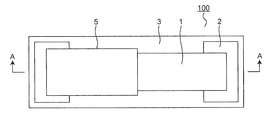
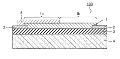
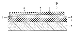
- FIG. 1 is a top view of an electromagnetic wave detector according to a first exemplary embodiment of the present invention, the whole being represented by 100, and FIG. 2 is a cross-sectional view when FIG. 1 is viewed in the AA direction. .
- the electromagnetic wave detector 100 is an electromagnetic wave detector 100 that detects an electromagnetic wave by photoelectric conversion, A substrate 4; An insulating layer 3 provided on the substrate 4; A graphene layer 1 provided on the insulating layer 3; A pair of electrodes 2 provided on the insulating layer 3 and connected to the graphene layer 1; A contact layer 5 provided in contact with the graphene layer 1, and
- the contact layer 5 is an electromagnetic wave detector made of a material having a polar group, and an electric charge is formed in the graphene layer 1 when the contact layer 5 contacts the graphene layer 1.
- the electromagnetic wave detector 100 includes a substrate 4 made of, for example, Si.
- the substrate 4 holds the entire electromagnetic wave detector 100, and is made of, for example, a high-resistance silicon substrate or a substrate with improved insulation by forming a thermal oxide film.
- a doped silicon substrate may be used to form a back gate.
- the thermal oxide film may also serve as the insulating layer 3.
- An insulating layer 3 made of, for example, silicon oxide (SiO 2 ), silicon nitride (SiN), aluminum oxide, nickel oxide, boron nitride (BN) or the like is provided on the substrate 4. Since boron nitride has an atomic arrangement similar to that of graphene, it does not hinder the charge transfer in the graphene by contact with the graphene, and does not hinder the performance of the graphene such as electron mobility.
- a pair of electrodes 2 are provided on the insulating layer 3.
- the pair of electrodes 2 is provided so as to be connected to both ends of the graphene layer 1 formed on the electrode 2.
- the electrode 2 is made of a metal such as Au, Ag, Cu, Al, Ni, Cr, or Pd.
- An adhesion film (not shown) made of Cr or Ti may be formed between the electrode 2 and the underlying insulating layer 3.
- the shape of the electrode 2 is not particularly limited as long as it has a size and thickness that can output an electric signal.
- the graphene layer 1 is provided on the insulating layer 3.
- the graphene layer 1 is composed of a single layer or two or more layers of graphene. When the number of graphene layers is increased, the light absorption rate is increased, and the sensitivity of the electromagnetic wave detector 100 is increased.
- Graphene is a monoatomic layer of a two-dimensional carbon crystal, and the thickness of the monolayer graphene is as thin as 0.34 nm per one carbon atom. Graphene has carbon atoms in each chain arranged in a hexagonal shape.
- the orientation of the lattice vectors of the hexagonal lattice does not have to be the same for any two layers of graphene included in the stacked structure, that is, there is a deviation in the orientation. May be. Further, it may be a laminated structure in which the directions of the lattice vectors are completely the same. In particular, when two or more layers of graphene are stacked, a band gap is formed, so that a wavelength selection effect can be provided.
- nanoribbon-shaped graphene when used, a graphene nanoribbon alone or a structure in which a plurality of graphene nanoribbons are arranged may be used.
- the graphene layer 1 may be non-doped, but may be doped p-type or n-type.
- a contact layer 5 is provided on the graphene layer 1.
- the contact layer 5 is made of a material containing a polar group.
- the polar group is classified into an electron withdrawing group and an electron donating group.
- the electron withdrawing group has an effect of decreasing the electron density
- the electron donating group has an effect of increasing the electron density.
- Examples of the electron withdrawing group include a halogen, a nitrile, a carboxyl group, and a carbonyl group.
- Examples of the electron donating group include an alkyl group, an alcohol, an amino group, and a hydroxyl group.
- a polymer material having polarity and the like in which the charge is biased in the whole molecule due to the polar group, can be applied to the contact layer 5.
- the metal, the semiconductor, the insulator, the two-dimensional material, or any mixture thereof a material having a polarity due to the polarization of electric charge in the molecule can be applied to the contact layer 5.
- the contact layer 5 has an OH group
- an electron donating property is generated by the resonance effect of the OH group, and n-type doping becomes possible.
- the contact layer 5 has a carboxyl group
- electron withdrawing property is generated by the carboxyl group, and p-type doping becomes possible.
- Doping is accelerated by supplying carriers generated by such a redox reaction to graphene.
- the contact layer 5 is provided on the graphene layer 1, and the graphene layer 1 and the contact layer 5 come into contact with each other, so that the graphene layer 1 forms a charge in the contact region 1a where the charge is formed.
- region 1b which is not performed will be included.
- a composition containing a novolak resin and a photosensitive agent having a quinonediazite group generally called a positive photoresist
- a positive photoresist for the contact layer 5
- the contact layer 5 can be formed only by photolithography, so that process damage can be reduced and the process can be simplified.
- the film thickness of the contact layer 5 is preferably as thin as possible within a range in which doping is possible so that photoelectric conversion can be performed when the graphene layer 1 is irradiated with electromagnetic waves.
- the expression “layer” is used for the contact layer 5, a monomolecular film or the like may be used as long as the graphene layer 1 can be doped, and the layer may not be strictly a layer.
- the contact layer 5 does not need to be solid, and may be in a liquid or gas state as long as doping is possible.
- the contact layer 5 is preferably formed so as to cover the boundary between the graphene layer 1 and the electrode 2.
- An electron density gradient is generated at the boundary portion where the graphene layer 1 and the electrode 2 are in contact with each other, and becomes a resistance when a current is extracted from the electrode 2.
- the contact layer 5 is formed so as to cover the boundary between the electrode 2 and the graphene layer 1
- an electron density gradient due to the contact layer 5 is added to the electron density gradient generated between the electrode 2 and the graphene layer 1.
- the density gradient is formed in a step shape, and the current extraction efficiency is improved.
- a structure in which the contact layer 5 does not cover the boundary between the graphene layer 1 and the electrode 2 may be employed.
- an output amplifier circuit (not shown) using graphene may be provided in an adjacent portion or a lower layer portion of the electromagnetic wave detector 100. Accordingly, the operation is faster than that of an output amplifier circuit formed from a silicon-based semiconductor material, and a high-performance electromagnetic wave detector can be realized.
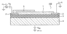
- the electromagnetic wave detector 100 In the operating state of the electromagnetic wave detector 100, a photocurrent generated by the incidence of the electromagnetic wave on the graphene layer 1 may be detected. In that case, the electromagnetic wave detector 100 operates with or without applying an external bias between the electrodes 2 at both ends of the photocurrent generation path of the graphene layer 1. However, the detection efficiency of the generated carriers is increased by applying a bias.
- An electrical circuit for taking out a change in photocurrent such as an external bias is connected to the graphene layer 1 through an electrode 2.
- a voltage is applied to V d between two electrodes 2, in response to an electrical signal that the resistance value changes within the graphene layer 1, the amount of current flowing between the electrodes 2 I d Changes.
- a circuit that allows a constant current to flow between the two electrodes 2 may be added to detect the amount of change in the voltage value.
- an electrical signal may be taken out as a transistor structure by combining the back surface of the substrate 4 with the back gate terminal and the two-terminal electrode 2.
- an even larger electric field can be generated in the graphene layer 1, and carriers generated by the incidence of electromagnetic waves can be detected with high efficiency.
- only one of the pair of electrodes 2 may be formed, and the potential change of the graphene layer 1 due to the incidence of electromagnetic waves may be detected using this.
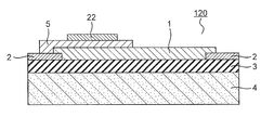
- the gate electrode 22 may be formed on the contact layer 5 or the graphene layer 1.
- the contact layer 5 can be used as a gate insulating layer. Therefore, by forming the gate electrode 22 directly on the contact layer 5 as shown in FIG. Can be easily formed.
- the contact layer 5 is not an insulator
- the gate electrode 22 may be formed on the protective film.
- a protective film 7 may be formed so as to cover the graphene layer 1, the contact layer 5, and the electrode 2.
- the contact layer 5 is made of a thin film such as a natural oxide or an organic substance
- the protective film 7 can be provided to prevent the property of the contact layer 5 from changing due to the influence of the surrounding atmosphere.
- the protective film 7 is made of an insulating film such as silicon oxide (SiO 2 ), aluminum oxide (Al 2 O 3 ), or silicon nitride (SiN). At this time, it is desirable to select a material that transmits the detected electromagnetic wave as the material of the protective film 7.
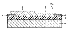
- the pair of electrodes may be formed of different metals such as an electrode 8 (for example, a source electrode) and an electrode 9 (for example, a drain electrode).
- Graphene has a different Fermi level or different contact resistance depending on the type of metal in contact. Therefore, when the electrode 8 and the electrode 9 are formed from different metals, the energy gap differs between the source and the drain. As a result, a bias is generated between the electrodes 8 and 9 by the carriers generated by the light irradiation, the photocurrent is increased, and the sensitivity can be improved.
- the pair of electrodes 2 are formed and the electric resistance between them is detected has been described as an example.
- other structures such as a transistor structure are applied. It doesn't matter.
- the contact layer 5 is provided on the top of the graphene layer 1.
- the contact layer 5 is formed of a material having polarity, charge transfer occurs in the graphene layer 1 according to the polarity.
- the graphene layer 1 in contact with the contact layer 5 is doped according to the polarity of the contact layer 5.
- an electron donating group and an electron withdrawing group as polar groups, it is possible to dope the graphene layer 1 into both n-type and p-type.
- the contact layer 5 when the contact layer 5 includes a plurality of polar groups, the polar group having the greatest influence causes a charge bias in the molecule. If the charge is biased throughout the molecule, the contact layer 5 can be used even if the opposite polar groups are included.
- the contact region 1a that is in contact with the contact layer 5 and the non-contact region 1b that is not in contact with the contact layer 5 are provided. Is formed.
- the electron density is different between the contact region 1 a and the non-contact region 1 b due to doping from the contact layer 5. Thereby, a gradient of electron density is generated inside the graphene layer 1.
- photocarriers are generated by light irradiation in the same manner as a pn junction in a general semiconductor.
- the electromagnetic wave detector 100 according to the first exemplary embodiment of the present invention by providing the contact layer 5 on the graphene layer 1, the photocurrent at the time of light irradiation is increased, and the detection sensitivity is improved.
- the electron density gradient formed in the graphene layer 1 is not necessarily a pn junction, and detection sensitivity is improved if an electron density gradient is formed even a little.
- the graphene layer 1 can be doped p-type if a material having an electron withdrawing group is used as the material of the contact layer 5 and n-type if a material having an electron donating group is used.
- the graphene layer 1 can be doped n-type, so that it can also be applied to CVD graphene having p-type conductivity, and by transferring the CVD graphene onto the electrode, Process damage can be reduced.
- polarity conversion can be selectively caused by photolithography, EB exposure processing, or the like. Therefore, it is not necessary to form a layer that protects the non-contact region when forming the contact layer, and not only the opening area of the graphene layer is increased, but also process damage can be reduced.
- the manufacturing method of the electromagnetic wave detector 100 includes the following steps 1 to 5.
- Step 1 A flat substrate 4 such as silicon is prepared.
- Step 2 The insulating layer 3 is formed on the substrate 4.
- the insulating layer 3 may be formed by thermally oxidizing the substrate 4 to form silicon oxide (SiO 2 ).
- another insulating film may be formed by a CVD method or a sputtering method.
- Step 3 An electrode 2 made of Au, Ag, Cu, Al, Ni, Cr or the like is formed. At this time, an adhesion film (not shown) made of Cr or Ti may be formed between the insulation film 3 and the electrode 2 in order to improve adhesion with the lower insulation layer 3.
- the electrode 2 is formed by, for example, forming a resist mask using photoengraving or EB drawing, and then depositing a metal layer thereon by vapor deposition or sputtering, and finally removing the metal layer on the resist mask by lift-off. And do it.
- Graphene is formed on the electrode 2 and the insulating layer 3.
- Graphene may be formed by epitaxial growth, or the formed graphene layer may be transferred and pasted in advance using a CVD method. Alternatively, graphene peeled by mechanical peeling or the like may be transferred. Subsequently, graphene is covered with a resist mask by photolithography or the like, and is patterned by etching with oxygen plasma. As a result, the graphene layer 1 is formed by removing unnecessary portions of graphene other than the channel portion and the region in contact with the electrode 2.
- a photoresist layer is formed on the electrode 2 and the graphene layer 1.
- the photoresist layer is made of a composition containing, for example, a photosensitizer having a quinonediazito group and a novolac resin.
- the photoresist layer is exposed and patterned by being immersed in an alkaline developer to selectively leave the photoresist layer on the graphene layer 1 to form the contact layer 5.
- the graphene layer 1 below the contact layer 5 is doped p-type by the polar group of the photoresist, and the portion of the graphene layer 1 where the contact layer 5 does not exist is doped n-type by exposure / development processing.
- the electromagnetic wave detector 100 according to the first exemplary embodiment of the present invention is completed through the above steps 1 to 5.
- the graphene layer 1 is formed on the electrode 2 here, a structure in which the graphene layer 1 is previously formed on the insulating film 3 and then the electrode 2 is formed as shown in FIG. 8 may be used.
- the contact layer 5 on the graphene layer 1 by a coating method by using a polymer having polarity instead of the photoresist as the material of the contact layer 5, and the contact layer can be formed by a simple process. 5 can be produced.
- the contact layer 5 is made of a material that converts the polarity chemically or a material that changes the polarity by electromagnetic wave irradiation.
- the structure of the electromagnetic wave detector is the same as, for example, the electromagnetic wave detector 100 shown in FIG.
- Polar conversion is a phenomenon in which a polar group is chemically converted, for example, an electron withdrawing group changes to an electron donating group, an electron donating group changes to an electron withdrawing group, and a polar group changes to a nonpolar group. Or a nonpolar group changes to a polar group.
- a polar group changes to a polar group.
- the polarity of the contact layer 5 is changed, electrons or holes generated during the conversion are supplied to the graphene.
- the graphene layer 1 in contact with the contact layer 5 is doped to form a contact region.
- the contact region of the graphene layer 1 that has been in contact with the contact layer 5 remains doped, so that an electron density gradient can be formed without the contact layer 5. It is. Thereby, the area which the graphene layer 1 opens with respect to incident light increases, and detection sensitivity improves.
- the contact layer 5 is made of a material that undergoes polarity conversion by electromagnetic wave irradiation, it is possible to selectively cause polarity conversion in the contact layer 5 by an exposure process or the like, and select the doping region. It can have sex. Thereby, doping regions (contact regions) with various patterns can be formed in the graphene layer 1 without forming a mask.
- polarity conversion can be generated only during light irradiation, an electron density gradient can be formed, and the photocurrent can be increased. These improve the detection sensitivity of the electromagnetic wave detector.
- the graphene layer 1 can be similarly doped when an oxidation-reduction reaction occurs in the contact layer 5 due to electromagnetic wave irradiation and electrons or holes are generated during the oxidation-reduction reaction.
- FIG. 9 shows electrical characteristics of the electromagnetic wave detector according to the second exemplary embodiment of the present invention.
- the horizontal axis represents the back gate voltage
- the vertical axis represents the current flowing between the two electrodes 2.
- the graphene layer 1 is composed of a single layer of graphene, the distance between the two electrodes 2 is 50 ⁇ m, and the length of the electrode 2 (vertical direction in FIG. 1) is 50 ⁇ m.
- the electrode 2 has a multilayer structure of metal whose outermost surface is made of gold and has a thickness of 30 nm.
- a 10 nm thick Cr film is formed between the electrode 2 and the insulating layer 3 in order to improve adhesion.
- the substrate 4 is made of p-type doped silicon. The substrate 4 operates as a back gate type in which a voltage is applied from the back surface.
- one of the two electrodes 2 is a source, the other is a drain, and a voltage is applied from the back surface of the substrate 4 to operate as a back gate.
- Insulating layer 3 is made of a thermal oxide film of silicon (SiO 2), a thickness of 290 nm.
- the contact layer 5 is a positive photoresist (for example, OFPR-800LB manufactured by Tokyo Ohka Kogyo Co., Ltd.) and is formed on the graphene layer 1 by exposure and development processing.
- the above-mentioned dimension is a dimension of the sample used for the measurement of FIG. 9, and the electromagnetic wave detector according to the embodiment of the present invention is not limited to these dimensions, and the sensitivity of the electromagnetic wave detector, etc. It is designed appropriately according to
- FIG. 9 shows the current flowing between the two electrodes 2 when the back gate voltage is changed, and two kinds of Dirac points, that is, a Dirac point by n-type doping and a Dirac point by p-type doping appear.
- a graphene layer produced by a CVD method is usually doped p-type.
- the graphene layer 1 is doped n-type in the process of converting the polarity of the quinonediazite group, which is a photosensitizer in the resist, to a carboxyl group.
- FIG. 10 is a graph comparing the photoresponse characteristics before and after forming the contact layer 5 for the electromagnetic wave detector according to the second exemplary embodiment of the present invention.
- the back gate voltage of the electromagnetic wave detector is ⁇
- a change in the source / drain current is shown when the white LED is irradiated with a constant period in a state where the voltage is 10 V and the source / drain voltage is 0.1 V.
- the horizontal axis represents the irradiation time of the white LED, and the vertical axis represents the source / drain current.
- the solid line indicates that the contact layer 5 is formed and a part of the graphene layer 1 is doped n-type.
- the dotted line indicates that the graphene layer 1 is not doped before the contact layer 5 is formed (graphene layer). 1 as a whole is p-type).
- the current value when the graphene layer 1 is doped is about three times the current value when the graphene layer 1 is not doped (before the contact layer 5 is formed). ing.
- FIG. 11 and 12 are cross-sectional views of the electromagnetic wave detector according to the third exemplary embodiment of the present invention, the whole being represented by 300 and 350, when viewed in the same direction as the AA direction of FIG. 11 and 12, the same reference numerals as those in FIG. 2 indicate the same or corresponding portions.
- both end portions are covered with the contact layer 5 except for the central portion of the graphene layer 1. Except for the position where the contact layer 5 is provided, the other structure is the same as that of the electromagnetic wave detector 100 according to the first exemplary embodiment.
- the graphene layer 1 formed by the CVD method the graphene layer 1 is usually doped p-type. For this reason, the contact layer 5 comes into contact with a part of the p-type graphene layer 1 to change the graphene layer 1 into an n-type region, whereby the graphene layer 1 can have an npn structure or a pnp structure.
- the graphene layers 1 at both ends covered by the contact layer 5 are n-type, and the central graphene layer 1 not covered by the contact layer 5 remains p-type. That is, an npn junction is formed in the graphene layer 1.
- the central portion of the graphene layer 1 is covered with the contact layer 5 in the electromagnetic wave detector 350 shown in FIG.
- the central graphene layer 1 covered by the contact layer 5 is n-type, and the graphene layers 1 at both ends not covered by the contact layer 5 remain p-type. That is, a pnp junction is formed in the graphene layer 1.
- the graphene layer 1 can further suppress dark current by using two or more layers of graphene or a two-dimensional material having a band gap.
- the graphene layer 1 formed on, for example, SiC doped with n-type it is desirable to use the p-type contact layer 5 which is a counter electrode to the n-type.
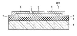
- FIG. 13 is a cross-sectional view of another electromagnetic wave detector according to the third exemplary embodiment of the present invention, the whole of which is represented by 380, when viewed in the same direction as the AA direction of FIG.
- the same reference numerals as those in FIG. 2 denote the same or corresponding parts.
- the electromagnetic wave detector 380 there are alternately a plurality of contact regions and non-contact regions in the graphene layer 1 formed by the contact layer 5 formed on the graphene layer 1.
- an electron density gradient is formed at the interface between the contact region under the contact layer 5 in the graphene layer 1 and the non-contact region where the contact layer 5 is not in contact.
- a density gradient is formed.
- the photocurrent generated by electromagnetic wave irradiation is increased by the number of interfaces between the contact area and the non-contact area, and the detection sensitivity is increased.
- the photocurrent can be increased by forming a large number of interfaces between the contact region and the non-contact region.
- the contact layers 5 to be formed may be arranged periodically or randomly.
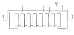
- FIG. 14 is a top view of the electromagnetic wave detector according to the fourth exemplary embodiment of the present invention, the whole being represented by 400, and FIG. 15 is a view when the electromagnetic wave detector of FIG. 14 is viewed in the BB direction. It is sectional drawing. 14 and 15, the same reference numerals as those in FIGS. 1 and 2 indicate the same or corresponding portions.
- a plurality of contact layers 5 are provided on the graphene layer 1 from one electrode 2 toward the other electrode 2 at a constant period. That is, as shown in FIG. 14, the contact layers 5 are arranged at equal intervals between the pair of electrodes 2.
- the contact layer 5 is a material that causes surface plasmon resonance by electromagnetic wave irradiation, polarization dependency is generated by making the contact layer 5 have a one-dimensional periodic structure. As a result, an electromagnetic wave detector that detects only specific polarized light can be formed.
- the contact layer 5 is disposed in the horizontal direction with respect to the electrode 2, but it may be disposed in the vertical direction or may have an angle.
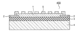
- FIG. 16 is a top view of another electromagnetic wave detector according to the fourth exemplary embodiment of the present invention, indicated as a whole by 450, and FIG. 17 is a view of the electromagnetic wave detector of FIG. 16 in the CC direction. It is sectional drawing in the case. 16 and 17, the same reference numerals as those in FIGS. 1 and 2 indicate the same or corresponding portions.
- the contact layer 5 has a two-dimensional periodic structure.
- the contact layer 5 is a material that causes surface plasmon resonance by electromagnetic wave irradiation
- by using such a periodic structure only an electromagnetic wave having a specific resonance wavelength can be strongly detected, and the detection sensitivity of the specific wavelength can be increased.
- the period, shape, and size of the contact layer 5 may be arbitrarily changed according to the resonance wavelength, or may be formed randomly. When formed randomly, plasmon resonance can be generated at multiple wavelengths, and the detection sensitivity can be increased for electromagnetic waves of multiple wavelengths.
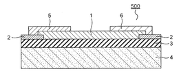
- FIG. 18 is a cross-sectional view of the electromagnetic wave detector according to the fifth exemplary embodiment of the present invention, the whole being represented by 500.
- FIG. 19 is a cross-sectional view of another electromagnetic wave detector according to the fifth exemplary embodiment of the present invention, the whole of which is represented by 550. Both are cross-sectional views when viewed in the same direction as the AA direction in FIG. 1.
- the same reference numerals as those in FIG. 2 indicate the same or corresponding portions.
- the electromagnetic wave detector 300 has the same structure as the electromagnetic wave detector 300 according to the third embodiment except that the contact layers 5 and 6 are made of different materials.
- the contact layer 5 is p-type and the contact layer 6 is n-type, an electron density gradient can be formed between the paired electrodes 2, the photocurrent extraction efficiency is improved, and the detection sensitivity is improved. Will improve.
- the p-type contact layer 5 and the n-type contact layer 6 are arranged on the graphene layer 1 so that the graphene layer 1 does not depend on the doping concentration or the conductivity type.
- a pnp structure can be formed.
- the contact layer 5 is p-type and the contact layer 6 is n-type here, the present invention is not limited to this.
- the formation of the contact layer 5 is effective as long as an electron density gradient is formed in the graphene layer 1.
- the contact layers 5 and 6 are n-type and p-type, n-type and n + type, and p-type. and it may be a combination of the p + -type like.
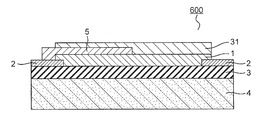
- FIG. 20 is a cross-sectional view of the electromagnetic wave detector according to the sixth exemplary embodiment of the present invention, the whole of which is represented by 600.
- FIG. 21 is a cross-sectional view of another electromagnetic wave detector according to the sixth embodiment of the present invention, the whole of which is represented by 650.
- Each is a cross-sectional view when viewed in the same direction as the AA direction in FIG. 1.
- the same reference numerals as those in FIG. 2 indicate the same or corresponding portions.
- a graphene layer 31 is further provided on the contact layer 5, and the upper and lower graphene layers 1 and 31 are sandwiched between the contact layer 5 and the electromagnetic wave detector 600 shown in FIG.
- a contact region and a non-contact region are formed by the contact layer 5 in the upper graphene layer 31 and the lower graphene layer 1, respectively, and an electron density gradient is formed.
- photoelectric conversion is performed in both the upper and lower graphene layers 1 and 31, and the photocurrent is increased by the electron density gradient, thereby improving the detection sensitivity.
- the end portion of the contact layer 5 is not covered with the upper graphene layer 31.
- Another graphene layer 31 may be provided so as to cover the contact layer 5 and the graphene layer 1.
- FIG. 22 is a cross-sectional view of the electromagnetic wave detector according to the seventh exemplary embodiment of the present invention, the whole of which is represented by 700. 22 is a cross-sectional view when viewed in the same direction as the AA direction in FIG. 1. In FIG. 22, the same reference numerals as those in FIG. 2 indicate the same or corresponding portions.
- the contact layer 5 is provided between the insulating layer 3 and the graphene layer 1. That is, the contact layer 5 is provided between the graphene layer 1 and the insulating layer 3.
- a material that does not transmit electromagnetic waves can be used as the material of the contact layer 5.
- visible light when visible light is used as input light, even if a material that does not transmit visible light is used as the contact layer 5, it is possible to reach the graphene layer 1 without attenuating the input light.
- process damage to the graphene layer 1 can be prevented.
- process damage can be effectively prevented by transferring the graphene layer 1 after forming the contact layer 5.
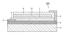
- FIG. 23 is a cross-sectional view of the electromagnetic wave detector according to the eighth exemplary embodiment of the present invention, the whole of which is represented by 800.
- FIG. 24 is a cross-sectional view of another electromagnetic wave detector according to the eighth embodiment of the present invention, the whole of which is represented by 850.
- 23 and 24 are cross-sectional views when viewed in the same direction as the AA direction in FIG. 1.
- the same reference numerals as those in FIG. 2 indicate the same or corresponding portions.
- the contact layer 5 is directly provided on the insulating layer 3, the graphene layer 1 is formed thereon, and the contact layer 6 is further provided thereon. That is, the contact layers 5 and 6 are made of different materials, and the two contact layers 5 and 6 made of different materials are arranged with the graphene layer 1 interposed therebetween. That is, the contact layers 5 and 6 are formed of two different materials, and the graphene layer 1 is sandwiched from above and below by the contact layers 5 and 6. For example, by using a p-type material for the contact layer 5 and an n-type material for the contact layer 6, an electron density gradient can be formed in the graphene layer 1, the photocurrent extraction efficiency is improved, and the detection sensitivity is improved. To do.
- a pin junction can be formed by forming a region where the contact layer 5 and the contact layer 6 face each other with the graphene layer 1 interposed therebetween (a region overlapping when viewed from above).
- photoelectric conversion can be performed efficiently, the photocurrent is increased, and the detection sensitivity is improved.
- the regions where the contact layer 5 and the contact layer 6 face each other with the graphene layer 1 interposed therebetween are p-type and n-type contact layers from above and below. Therefore, an electrically neutral i layer is formed.
- the contact layers 5 and 6 are formed of two different materials, and the contact layer 5, the graphene layers 1 and 31, and the contact layer 6 are sequentially stacked on the insulating layer 3. Yes.
- the pair of electrodes 2 are provided on the insulating layer 3 and the contact layer 6, respectively.
- the graphene layer 1 is doped p-type and the graphene layer 31 is doped n-type.
- an electric field can be applied in a direction perpendicular to the interface between the graphene layer 1 and the graphene layer 31.
- a pn heterojunction can be formed in the vertical direction, thereby enabling an OFF operation.
- Such a structure is more effective when applied to two-layer graphene having a band gap or a two-dimensional material.
- the graphene layer 1 and the electrode 2 are not in direct contact, but a structure in which these are in direct contact may be used. In that case, the electric field applied to the graphene layer 1 decreases, but the amount of current flowing increases.
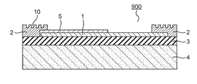
- FIG. 25 is a cross-sectional view of the electromagnetic wave detector according to the ninth exemplary embodiment of the present invention, the whole of which is represented by 900, when viewed in the same direction as the AA direction in FIG.
- the same reference numerals as those in FIG. 2 indicate the same or corresponding parts.
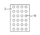
- FIG. 26 is a top view of the electrode 2 of the electromagnetic wave detector 900.
- the electrode 2 has a periodic structure composed of the periodic recesses 10, and an electromagnetic wave having a specific wavelength resonates in accordance with the periodic structure.
- Other structures are the same as those of the electromagnetic wave detector 100 according to the first exemplary embodiment.
- the cylindrical recesses 10 are arranged in two orthogonal directions.
- the arrangement of the recesses 10 may be any arrangement as long as it is a periodic arrangement such as a square lattice or a triangular lattice.
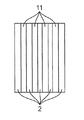
- the shape of the concave portion 10 may be other shapes such as a prism, a triangular prism, a quadrangular prism, and an elliptical cylinder in addition to the cylinder. Further, as shown in FIG.
- the recess 11 may be a one-dimensional groove arranged in parallel.
- the cross-sectional shape of the groove is not limited to a rectangle, but may be a triangle or the like.
- plasmon resonance occurs in these recesses 10 and 11 regardless of whether or not they penetrate the electrode 2.
- the electromagnetic wave having a wavelength to be detected may be appropriately designed so as to plasmon resonate.
- the material of the electrode 2 may be any metal as long as surface plasmon resonance occurs. For example, Au, Ag, Al, or the like is used.
- periodic concave portions 10 and 11 are formed on the surface of the electrode 2
- periodic convex portions may be formed. Plasmon resonance with the same effect occurs.
- the resonance wavelength of the plasmon resonance is determined depending on the periodic structure of the recess 10 or the like.
- the electromagnetic wave detector 900 can strongly detect only an electromagnetic wave having a specific resonance wavelength, and the detection sensitivity of the specific wavelength can be increased.
- FIG. 28 and 29 are top views of the graphene layer 1 used in the electromagnetic wave detector according to the tenth embodiment of the present invention.
- the graphene layer 1 has a periodic structure including periodic recesses 10, and electromagnetic waves having a specific wavelength resonate with each other according to the periodic structure.
- the concave portion 12 is a cylindrical hole periodically arranged in two orthogonal directions, and the concave portion 13 is a one-dimensional groove arranged in parallel.
- Other structures are the same as those of the electromagnetic wave detector 100 according to the first exemplary embodiment.
- the recesses 12 and 13 may be holes penetrating the graphene layer 1. That is, when the graphene layer 1 is a single layer, the recesses 12 and 13 are holes that penetrate the graphene layer 1, and when the graphene layer 1 is a plurality of layers, all of the recesses 12 and 13 are holes that only penetrate some of the layers. It may be a hole penetrating the layer.
- the two-dimensional periodic arrangement of the recesses 12 may be any periodic arrangement such as a square lattice or a triangular lattice.
- the shape of the recess 12 may be a recess of any shape such as a cylinder, a prism, a triangle, a quadrangle, or an elliptical column.
- the shape viewed from above, such as a triangular prism is asymmetrical, the light absorbed by the graphene layer 1 has polarization dependency, so that an electromagnetic wave detector that detects only specific polarized light can be formed.
- the one-dimensional periodic arrangement is a one-dimensional groove arranged in parallel as shown in FIG. 29, for example.
- the cross-sectional shape of the groove is not limited to a rectangle, but may be a triangle or the like.
- the electromagnetic wave detector having such an asymmetric structure can be applied to polarization imaging.
- Polarization imaging makes it possible to distinguish between object boundaries, artifacts and natural objects.
- it is necessary to attach other components to the electromagnetic wave detector such as a polarizer and a polarizing filter, which increases the size of the device and system.
- the electromagnetic wave detector According to the embodiment of the present invention, an electromagnetic wave detector that detects a specific polarized light can be realized by forming an asymmetric recess in the graphene layer 1, so that the system can be downsized and the number of parts can be reduced. This has effects such as reduction and elimination of light loss due to a polarizer and a filter.
- Embodiment 11 FIG.
- the electromagnetic wave is incident on the graphene layer 1 and the photocurrent generated thereby is detected.
- the graphene layer instead of 1, a layer of a two-dimensional material made of transition metal dichalcogenide, black phosphorous, or the like is used.
- the electromagnetic wave detector according to the embodiment of the present invention is an electromagnetic wave detector that detects an electromagnetic wave by photoelectric conversion, A substrate 4; An insulating layer 3 provided on the substrate 4; A two-dimensional material layer 1 made of a transition metal dichalcogenide or black phosphorus provided on the insulating layer 3; A pair of electrodes 2 provided on the insulating layer 3 and connected to the two-dimensional material layer 1; A contact layer 5 provided in contact with the two-dimensional material layer 1, The contact layer 5 is made of a material having a polar group, and an electric charge is formed in the two-dimensional material layer 1 when the contact layer 5 contacts the two-dimensional material layer 1.
- the structure is the same as that of the electromagnetic wave detector 100 except that the graphene layer is replaced with a two-dimensional material layer.
- Transition metal dichalcogenide, black phosphorus, and the like are called two-dimensional materials because they have the same atomic layer structure as graphene, and are made of, for example, transition metal dichalcogenides such as MoS 2 , WS 2 , WSe 2, or black phosphorus.
- the two-dimensional material layer may have a structure in which layers of the same kind of materials or different materials are laminated. Alternatively, a stacked structure of probeskite and graphene or different two-dimensional materials may be used.
- transition metal dichalcogenide materials and black phosphorus have a predetermined band gap. For this reason, since the off-current becomes almost zero, the noise of the electromagnetic wave detector is reduced, and the performance of the electromagnetic wave detector can be improved.
- the size of the band gap can be adjusted according to the number of layers. For this reason, the wavelength of the electromagnetic wave to be detected can be selected depending on the number of layers. Thereby, the wavelength selective electromagnetic wave detector which detects only the electromagnetic waves of a specific wavelength can be obtained.
- the size of the band gap can be controlled by the number of laminated two-dimensional material layers, and the composition of the semiconductor material is different from that of a detector using a conventional semiconductor. Since it is not necessary to control the size of the band gap, it becomes easy to control the size of the band gap. Further, since it is not necessary to use an optical filter that is a typical wavelength selection method, the number of optical components can be reduced, and the loss of incident light due to passing through the filter can also be reduced.
- two-dimensional materials such as transition metal dichalcogenides and black phosphorus are combined in two or more different materials, or two-dimensional materials such as transition metal dichalcogenide and black phosphorus are combined with graphene to form a heterojunction.
- FIG. FIG. 30 is a top view of the array sensor according to the twelfth embodiment of the present invention, represented as a whole by 1000, and is an array sensor in which electromagnetic wave detectors are arranged in an array.
- the electromagnetic wave detectors 100 according to the first exemplary embodiment of the present invention are arranged in 2 ⁇ 2, but the number to be arranged is not limited to this.
- the array sensor 1000 including the electromagnetic wave detector 100 using the graphene layer 1 can detect electromagnetic waves in a very wide wavelength range from ultraviolet light to microwaves. For this reason, for example, when the array sensor 1000 is applied to a vehicle-mounted sensor, it can be used as a visible light image camera during the day, while it can also be used as an infrared camera at night, and there is no need to use different cameras depending on the detection wavelength.
- FIG. 31 is a top view of another array sensor according to the twelfth embodiment of the present invention, the whole of which is represented by 2000.
- different types of electromagnetic wave detectors 100a, 100b, 100c, and 100d are arranged in 2 ⁇ 2, but the number to be arranged is not limited to this.
- the various electromagnetic wave detectors described in the first to eleventh embodiments are arranged in a one-dimensional or two-dimensional array so as to have a function as an image sensor. Can do.
- the electromagnetic wave detectors 100a, 100b, 100c, and 100d are formed from electromagnetic wave detectors having different detection wavelengths.
- the electromagnetic wave detectors having detection wavelength selectivity described in the ninth to eleventh embodiments are arranged in an array. Thereby, the array sensor 2000 can detect electromagnetic waves having different wavelengths by at least two or more.
- the electromagnetic wave detectors 100a to 100d having different detection wavelengths in an array like this, in the wavelength region of ultraviolet light, infrared light, terahertz wave, and radio wave as well as the image sensor used in the visible light region. A colorized image can be obtained.
- the structure of the array sensor 2000 makes it possible to manufacture an image sensor that detects the light intensity of electromagnetic waves having a plurality of wavelengths. As a result, it is possible to detect a plurality of wavelengths of electromagnetic waves and obtain a color image without using a color filter conventionally required for a CMOS sensor or the like.
- a polarization discrimination image sensor can be formed by arraying electromagnetic wave detectors having different polarizations to be detected. For example, an artifact and a natural object can be discriminated.
- FIG. FIG. 32 is a diagram of the camera system according to the twelfth embodiment of the present invention, the whole being represented by 10,000, and specifically, a black diagram of the camera system equipped with the array sensor 1000 or the array sensor 2000.
- the camera system 10000 according to the thirteenth embodiment of the present invention includes a lens, an optical system (shutter, aperture, filter, etc.), an array sensor (1000 or 2000), a signal processing system, and an image output system. Incident electromagnetic waves are collected by a lens and input to the array sensor. Further, the output obtained from the array sensor is signal-processed and output as an image.
- a visible lens, a near-infrared lens, an infrared lens, a terahertz lens, or the like is selected as necessary.
- light of various wavelengths can be input to the array sensor without a filter.
- a shutter, an aperture, a filter, and the like as an optical system may be selected as necessary, or may be omitted.
- no lens is used or when an ultra-wideband lens is used, all wavelengths can be detected by the array sensor.
- the transmitted wavelength does not depend on the material, and the transmitted wavelength can be selectively controlled by controlling the structure.
Landscapes
- Engineering & Computer Science (AREA)
- Physics & Mathematics (AREA)
- Power Engineering (AREA)
- Condensed Matter Physics & Semiconductors (AREA)
- Electromagnetism (AREA)
- General Physics & Mathematics (AREA)
- Computer Hardware Design (AREA)
- Microelectronics & Electronic Packaging (AREA)
- Chemical & Material Sciences (AREA)
- Inorganic Chemistry (AREA)
- Manufacturing & Machinery (AREA)
- Light Receiving Elements (AREA)
Abstract
Description
これに対して、バンドギャップがゼロまたは極めて小さいグラフェンを検出層に用いた電磁波検出器が提案されている(例えば、特許文献1参照)。
また、SiC基板上に、グラフェン層と、グラフェン層より大きな仕事関数を有する金属酸化物とを積層してグラフェン層中にpn接合領域を設けることにより、光電流を増加させる構造が提案されている(例えば、特許文献2参照)。 In the conventional electromagnetic wave detector, a semiconductor material is generally used as the detection layer. However, since the semiconductor material has a predetermined band gap, only an electromagnetic wave having energy larger than the band gap can be detected.
On the other hand, an electromagnetic wave detector using a graphene having a band gap of zero or extremely small as a detection layer has been proposed (see, for example, Patent Document 1).
Further, a structure has been proposed in which a photocurrent is increased by stacking a graphene layer and a metal oxide having a work function larger than that of the graphene layer on a SiC substrate to provide a pn junction region in the graphene layer. (For example, refer to Patent Document 2).
基板と、
基板の上に設けられた絶縁層と、
絶縁層の上に設けられたグラフェン層と、
絶縁層の上に設けられ、グラフェン層にそれぞれ接続された一対の電極と、
グラフェン層に接触するように設けられた接触層と、を含み、
接触層は極性基を持つ材料からなり、接触層がグラフェン層に接触することにより、グラフェン層中に電荷が形成されたことを特徴とする電磁波検出器である。 The present invention is an electromagnetic wave detector for photoelectrically detecting and detecting electromagnetic waves,
A substrate,
An insulating layer provided on the substrate;
A graphene layer provided on the insulating layer;
A pair of electrodes provided on the insulating layer and respectively connected to the graphene layer;
A contact layer provided in contact with the graphene layer,
The contact layer is made of a material having a polar group, and the contact layer is an electromagnetic wave detector characterized in that a charge is formed in the graphene layer by contacting the graphene layer.
図1は、全体が100で表される、本発明の実施の形態1にかかる電磁波検出器の上面図であり、図2は、図1をA-A方向に見た場合の断面図である。
FIG. 1 is a top view of an electromagnetic wave detector according to a first exemplary embodiment of the present invention, the whole being represented by 100, and FIG. 2 is a cross-sectional view when FIG. 1 is viewed in the AA direction. .
基板4と、
基板4の上に設けられた絶縁層3と、
絶縁層3の上に設けられたグラフェン層1と、
絶縁層3の上に設けられ、グラフェン層1にそれぞれ接続された一対の電極2と、
グラフェン層1に接触するように設けられた接触層5と、を含み、
接触層5は極性基を持つ材料からなり、接触層5がグラフェン層1に接触することにより、グラフェン層1中に電荷が形成されたことを特徴とする電磁波検出器である。 The
A
An insulating
A
A pair of
A
The
実施の形態2にかかる電磁波検出器では、接触層5は、化学的に極性変換する材料、または電磁波照射で極性変換する材料からなる。電磁波検出器の構造は、例えば図2に示す電磁波検出器100と同じである。
In the electromagnetic wave detector according to the second exemplary embodiment, the
図11、12は、全体が300、350で表される、本発明の実施の形態3にかかる電磁波検出器の、図1のA-A方向と同じ方向に見た場合の断面図である。図11、12中、図2と同一符合は、同一または相当箇所を示す。
11 and 12 are cross-sectional views of the electromagnetic wave detector according to the third exemplary embodiment of the present invention, the whole being represented by 300 and 350, when viewed in the same direction as the AA direction of FIG. 11 and 12, the same reference numerals as those in FIG. 2 indicate the same or corresponding portions.
図14は、全体が400で表される、本発明の実施の形態4にかかる電磁波検出器の上面図であり、図15は、図14の電磁波検出器をB-B方向に見た場合の断面図である。図14、15中、図1、2と同一符合は、同一または相当箇所を示す。
FIG. 14 is a top view of the electromagnetic wave detector according to the fourth exemplary embodiment of the present invention, the whole being represented by 400, and FIG. 15 is a view when the electromagnetic wave detector of FIG. 14 is viewed in the BB direction. It is sectional drawing. 14 and 15, the same reference numerals as those in FIGS. 1 and 2 indicate the same or corresponding portions.
図18は、全体が500で表される、本発明の実施の形態5にかかる電磁波検出器の断面図である。また、図19は、全体が550で表される、本発明の実施の形態5にかかる他の電磁波検出器の断面図である。いずれも、図1のA-A方向と同じ方向に見た場合の断面図であり、図18、19中、図2と同一符合は、同一または相当箇所を示す。
FIG. 18 is a cross-sectional view of the electromagnetic wave detector according to the fifth exemplary embodiment of the present invention, the whole being represented by 500. FIG. 19 is a cross-sectional view of another electromagnetic wave detector according to the fifth exemplary embodiment of the present invention, the whole of which is represented by 550. Both are cross-sectional views when viewed in the same direction as the AA direction in FIG. 1. In FIGS. 18 and 19, the same reference numerals as those in FIG. 2 indicate the same or corresponding portions.
図20は、全体が600で表される、本発明の実施の形態6にかかる電磁波検出器の断面図である。また、図21は、全体が650で表される、本発明の実施の形態6にかかる他の電磁波検出器の断面図である。いずれも、図1のA-A方向と同じ方向に見た場合の断面図であり、図20、21中、図2と同一符合は、同一または相当箇所を示す。
FIG. 20 is a cross-sectional view of the electromagnetic wave detector according to the sixth exemplary embodiment of the present invention, the whole of which is represented by 600. FIG. 21 is a cross-sectional view of another electromagnetic wave detector according to the sixth embodiment of the present invention, the whole of which is represented by 650. Each is a cross-sectional view when viewed in the same direction as the AA direction in FIG. 1. In FIGS. 20 and 21, the same reference numerals as those in FIG. 2 indicate the same or corresponding portions.
図22は、全体が700で表される、本発明の実施の形態7にかかる電磁波検出器の断面図である。図22は、図1のA-A方向と同じ方向に見た場合の断面図であり、図22中、図2と同一符合は、同一または相当箇所を示す。
FIG. 22 is a cross-sectional view of the electromagnetic wave detector according to the seventh exemplary embodiment of the present invention, the whole of which is represented by 700. 22 is a cross-sectional view when viewed in the same direction as the AA direction in FIG. 1. In FIG. 22, the same reference numerals as those in FIG. 2 indicate the same or corresponding portions.
図23は、全体が800で表される、本発明の実施の形態8にかかる電磁波検出器の断面図である。また、図24は、全体が850で表される、本発明の実施の形態8にかかる他の電磁波検出器の断面図である。図23、24は、図1のA-A方向と同じ方向に見た場合の断面図であり、図23、24中、図2と同一符合は、同一または相当箇所を示す。
FIG. 23 is a cross-sectional view of the electromagnetic wave detector according to the eighth exemplary embodiment of the present invention, the whole of which is represented by 800. FIG. 24 is a cross-sectional view of another electromagnetic wave detector according to the eighth embodiment of the present invention, the whole of which is represented by 850. 23 and 24 are cross-sectional views when viewed in the same direction as the AA direction in FIG. 1. In FIGS. 23 and 24, the same reference numerals as those in FIG. 2 indicate the same or corresponding portions.
図25は、全体が900で表される、本発明の実施の形態9にかかる電磁波検出器を、図1のA-A方向と同じ方向に見た場合の断面図であり、図25中、図2と同一符合は、同一または相当箇所を示す。また、図26は、電磁波検出器900の電極2の上面図である。
FIG. 25 is a cross-sectional view of the electromagnetic wave detector according to the ninth exemplary embodiment of the present invention, the whole of which is represented by 900, when viewed in the same direction as the AA direction in FIG. The same reference numerals as those in FIG. 2 indicate the same or corresponding parts. FIG. 26 is a top view of the
図28、29は、本発明の実施の形態10にかかる電磁波検出器に用いられるグラフェン層1の上面図である。本実施の形態10にかかる電磁波検出器では、グラフェン層1は、周期的な凹部10からなる周期構造を有し、周期構造に応じて特定波長の電磁波がプラズモン共鳴する。凹部12は、直交する2方向に周期配置された円柱の孔であり、凹部13は、並列配置された1次元の溝である。他の構造は、実施の形態1にかかる電磁波検出器100と同じである。
28 and 29 are top views of the
実施の形態1~10にかかる電磁波検出器は、電磁波がグラフェン層1に入射し、これにより発生する光電流を検出しているが、本発明の実施の形態にかかる電磁波検出器では、グラフェン層1に代えて、遷移金属ダイカルコゲナイドや黒リン(Black Phosphorus)などからなる2次元材料の層を用いる。
In the electromagnetic wave detector according to the first to tenth embodiments, the electromagnetic wave is incident on the
基板4と、
基板4の上に設けられた絶縁層3と、
絶縁層3の上に設けられた、遷移金属ダイカルコゲナイドまたは黒リンからなる2次元材料層1と、
絶縁層3の上に設けられ、2次元材料層1にそれぞれ接続された一対の電極2と、
2次元材料層1に接触するように設けられた接触層5と、を含み、
接触層5は極性基を持つ材料からなり、接触層5が2次元材料層1に接触することにより、2次元材料層1中に電荷が形成される。グラフェン層が2次元材料層に置き換えられている以外は、電磁波検出器100と同じ構造である That is, the electromagnetic wave detector according to the embodiment of the present invention is an electromagnetic wave detector that detects an electromagnetic wave by photoelectric conversion,
A
An insulating
A two-
A pair of
A
The
図30は、全体が1000で表される、本発明の実施の形態12にかかるアレイセンサの上面図であり、電磁波検出器がアレイ状に配置されたアレイセンサである。図30に示すアレイセンサ1000では、本発明の実施の形態1にかかる電磁波検出器100が2×2に配置されているが、配置する個数はこれに限定されるものではない。
FIG. 30 is a top view of the array sensor according to the twelfth embodiment of the present invention, represented as a whole by 1000, and is an array sensor in which electromagnetic wave detectors are arranged in an array. In the
図32は、全体が10000で表される、本発明の実施の形態12にかかるカメラシステムのダイアグラムであり、具体的には、アレイセンサ1000またはアレイセンサ2000を搭載したカメラシステムのブラックダイアグラムである。本発明の実施の形態13にかかるカメラシステム10000は、レンズ、光学系(シャッター、アパーチャ、フィルタ等)、アレイセンサ(1000または2000)、信号処理システム、画像出力システム、で構成される。入射電磁波をレンズで集光し、アレイセンサに入力する。さらにアレイセンサから得られた出力を信号処理し、画像として出力する。レンズは、可視レンズ、近赤外レンズ、赤外レンズ、テラヘルツレンズ、などを必要に応じて選択する。レンズを切り替えることで、フィルタ無しで様々な波長の光をアレイセンサに入力することができる。このとき、光学系としてシャッター、アパーチャ、フィルタ等は必要に応じて選択しても良いし、無くても良い。また、レンズを使用しない場合や、超広帯域レンズを使用する場合は全ての波長をアレイセンサにて検出することが可能となる。
FIG. 32 is a diagram of the camera system according to the twelfth embodiment of the present invention, the whole being represented by 10,000, and specifically, a black diagram of the camera system equipped with the
2 電極
3 絶縁層
4 基板
5、6 接触層
7 保護膜
8、9 電極
10、11、12、13 凹部
100 電磁波検出器
1000、2000 アレイセンサ
10000 カメラシステム DESCRIPTION OF
Claims (15)
- 電磁波を光電変換して検出する電磁波検出器であって、
基板と、
該基板の上に設けられた絶縁層と、
該絶縁層の上に設けられたグラフェン層と、
該絶縁層の上に設けられ、該グラフェン層にそれぞれ接続された一対の電極と、
該グラフェン層に接触するように設けられた接触層と、を含み、
該接触層は極性基を持つ材料からなり、該接触層が該グラフェン層に接触することにより、該グラフェン層中に電荷が形成されたことを特徴とする電磁波検出器。 An electromagnetic wave detector for photoelectrically converting and detecting electromagnetic waves,
A substrate,
An insulating layer provided on the substrate;
A graphene layer provided on the insulating layer;
A pair of electrodes provided on the insulating layer and respectively connected to the graphene layer;
A contact layer provided in contact with the graphene layer,
The electromagnetic wave detector, wherein the contact layer is made of a material having a polar group, and an electric charge is formed in the graphene layer by the contact layer being in contact with the graphene layer. - 上記グラフェン層は、上記接触層が接触することにより電荷が形成された接触領域と、電荷が形成されない非接触領域と、を含むことを特徴とする請求項1に記載の電磁波検出器。 2. The electromagnetic wave detector according to claim 1, wherein the graphene layer includes a contact region in which a charge is formed by contact of the contact layer and a non-contact region in which no charge is formed.
- 上記接触層は、上記グラフェン層と上記電極との境界を覆うことを特徴とする請求項1または2に記載の電磁波検出器。 The electromagnetic wave detector according to claim 1, wherein the contact layer covers a boundary between the graphene layer and the electrode.
- 上記接触層は、化学的に極性変換する材料、または電磁波照射で極性変換する材料からなることを特徴とする請求項1~3のいずれかに記載の電磁波検出器。 The electromagnetic wave detector according to any one of claims 1 to 3, wherein the contact layer is made of a material that undergoes chemical polarity conversion or a material that undergoes polarity conversion by electromagnetic wave irradiation.
- 上記接触層は、極性を有するポリマー材料、ヒドロキシル基またはカルボキシル基を有する材料、電磁波照射によって酸化還元反応を生じる材料、キノンジアジト基を有する感光剤とノボラック樹脂とを含有する組成物材料、および極性を有する無機物材料、からなるグループから選択される材料であることを特徴とする請求項1~4のいずれかに記載の電磁波検出器。 The contact layer includes a polymer material having polarity, a material having a hydroxyl group or a carboxyl group, a material that causes a redox reaction upon irradiation with electromagnetic waves, a composition material containing a photosensitizer having a quinonediazite group and a novolac resin, and a polarity. The electromagnetic wave detector according to any one of claims 1 to 4, wherein the electromagnetic wave detector is a material selected from the group consisting of inorganic materials.
- 上記グラフェン層の上に、複数の上記接触層が設けられたことを特徴とする請求項1~5のいずれかに記載の電磁波検出器。 The electromagnetic wave detector according to any one of claims 1 to 5, wherein a plurality of the contact layers are provided on the graphene layer.
- 上記接触層がp型の上記グラフェン層の一部に接触して、該グラフェン層をn型領域に変えることにより、該グラフェン層がnpn構造またはpnp構造を有することを特徴とする請求項1~6のいずれかに記載の電磁波検出器。 The graphene layer has an npn structure or a pnp structure by contacting the contact layer with a part of the p-type graphene layer and changing the graphene layer into an n-type region. 6. The electromagnetic wave detector according to any one of 6.
- 上記接触層が、互いに異なる材料からなる複数の接触層からなることを特徴とすることを特徴とする請求項1~7のいずれかに記載の電磁波検出器。 The electromagnetic wave detector according to any one of claims 1 to 7, wherein the contact layer comprises a plurality of contact layers made of different materials.
- 互いに異なる材料からなる2つの上記接触層が、上記グラフェン層を挟んで対向することを特徴とする請求項8に記載の電磁波検出器。 The electromagnetic wave detector according to claim 8, wherein the two contact layers made of different materials face each other with the graphene layer interposed therebetween.
- 上記接触層が、上記グラフェン層の上に設けられ、更に該接触層と該グラフェン層を覆うように他のグラフェン層が設けられたことを特徴とする請求項1~8のいずれかに記載の電磁波検出器。 The contact layer is provided on the graphene layer, and another graphene layer is further provided so as to cover the contact layer and the graphene layer. Electromagnetic wave detector.
- 上記接触層は、上記絶縁層と上記グラフェン層との間に設けられたことを特徴とする請求項1~8のいずれかに記載の電磁波検出器。 The electromagnetic wave detector according to any one of claims 1 to 8, wherein the contact layer is provided between the insulating layer and the graphene layer.
- 上記電極は、周期的な凹部または凸部からなる周期構造を有し、該周期構造に応じて特定波長の電磁波がプラズモン共鳴することを特徴とする請求項1~11のいずれかに記載の電磁波検出器。 The electromagnetic wave according to any one of claims 1 to 11, wherein the electrode has a periodic structure including periodic concave portions or convex portions, and an electromagnetic wave having a specific wavelength resonates in accordance with the periodic structure. Detector.
- 上記グラフェン膜は、周期的な凹部または凸部からなる周期構造を有し、該周期構造に応じて特定波長の電磁波がプラズモン共鳴することを特徴とする請求項1~11のいずれかに記載の電磁波検出器。 12. The graphene film according to claim 1, wherein the graphene film has a periodic structure including periodic concave portions or convex portions, and an electromagnetic wave having a specific wavelength resonates in accordance with the periodic structure. Electromagnetic wave detector.
- 電磁波を光電変換して検出する電磁波検出器であって、
基板と、
該基板の上に設けられた絶縁層と、
該絶縁層の上に設けられた、遷移金属ダイカルコゲナイドまたは黒リンからなる2次元材料層と、
該絶縁層の上に設けられ、該2次元材料層にそれぞれ接続された一対の電極と、
該2次元材料層に接触するように設けられた接触層と、を含み、
該接触層は極性基を持つ材料からなり、該接触層が該2次元材料層に接触することにより、該2次元材料層中に電荷が形成されたことを特徴とする電磁波検出器。 An electromagnetic wave detector for photoelectrically converting and detecting electromagnetic waves,
A substrate,
An insulating layer provided on the substrate;
A two-dimensional material layer made of transition metal dichalcogenide or black phosphorus provided on the insulating layer;
A pair of electrodes provided on the insulating layer and respectively connected to the two-dimensional material layer;
A contact layer provided in contact with the two-dimensional material layer,
The electromagnetic wave detector, wherein the contact layer is made of a material having a polar group, and an electric charge is formed in the two-dimensional material layer by the contact layer contacting the two-dimensional material layer. - 請求項1~14のいずれかに記載の電磁波検出器が、アレイ状に配置されたことを特徴とするアレイセンサ。 An array sensor comprising the electromagnetic wave detector according to any one of claims 1 to 14 arranged in an array.
Priority Applications (5)
| Application Number | Priority Date | Filing Date | Title |
|---|---|---|---|
| US16/076,611 US11302834B2 (en) | 2016-02-24 | 2016-02-24 | Electromagnetic wave detector |
| PCT/JP2016/055485 WO2017145299A1 (en) | 2016-02-24 | 2016-02-24 | Electromagnetic wave detector |
| EP16891456.2A EP3422423B1 (en) | 2016-02-24 | 2016-02-24 | Electromagnetic wave detector |
| CN201680081193.5A CN108701737B (en) | 2016-02-24 | 2016-02-24 | Electromagnetic wave detector |
| JP2016554752A JP6113372B1 (en) | 2016-02-24 | 2016-02-24 | Electromagnetic wave detector |
Applications Claiming Priority (1)
| Application Number | Priority Date | Filing Date | Title |
|---|---|---|---|
| PCT/JP2016/055485 WO2017145299A1 (en) | 2016-02-24 | 2016-02-24 | Electromagnetic wave detector |
Publications (1)
| Publication Number | Publication Date |
|---|---|
| WO2017145299A1 true WO2017145299A1 (en) | 2017-08-31 |
Family
ID=58666646
Family Applications (1)
| Application Number | Title | Priority Date | Filing Date |
|---|---|---|---|
| PCT/JP2016/055485 WO2017145299A1 (en) | 2016-02-24 | 2016-02-24 | Electromagnetic wave detector |
Country Status (5)
| Country | Link |
|---|---|
| US (1) | US11302834B2 (en) |
| EP (1) | EP3422423B1 (en) |
| JP (1) | JP6113372B1 (en) |
| CN (1) | CN108701737B (en) |
| WO (1) | WO2017145299A1 (en) |
Cited By (8)
| Publication number | Priority date | Publication date | Assignee | Title |
|---|---|---|---|---|
| KR101940422B1 (en) * | 2017-10-02 | 2019-01-21 | 재단법인대구경북과학기술원 | Microwave photodetection device and method of manufacturing of microwave photodetection device |
| CN109273554A (en) * | 2018-08-30 | 2019-01-25 | 上海电力学院 | A kind of graphene-based built in field indium gallium arsenic detector |
| KR20190041742A (en) * | 2017-10-13 | 2019-04-23 | 건국대학교 산학협력단 | Phothdetector based on barristor and image sencor including the same |
| WO2020003564A1 (en) * | 2018-06-28 | 2020-01-02 | 三菱電機株式会社 | Electronic device using graphene, method of manufacturing same, and electromagnetic wave detector including same |
| JP2020077780A (en) * | 2018-11-08 | 2020-05-21 | 富士通株式会社 | Photo detection element, photosensor and method of manufacturing photo detection element |
| WO2021070594A1 (en) * | 2019-10-10 | 2021-04-15 | ソニーセミコンダクタソリューションズ株式会社 | Electromagnetic wave detection device, electromagnetic detection system, and electromagnetic detection method |
| JPWO2021124609A1 (en) * | 2019-12-17 | 2021-06-24 | ||
| JP2022054180A (en) * | 2020-09-25 | 2022-04-06 | 富士通株式会社 | Photodetector |
Families Citing this family (12)
| Publication number | Priority date | Publication date | Assignee | Title |
|---|---|---|---|---|
| JP6810753B2 (en) * | 2016-04-01 | 2021-01-06 | 中国科学院蘇州納米技術与納米▲ファン▼生研究所 | Black phosphorus crystal and its manufacturing method, photoelectric detector, two-dimensional black phosphorus PN junction and its manufacturing method and use |
| CN109884557B (en) * | 2019-01-15 | 2020-11-03 | 武汉大学 | Magnetic sensor based on graphene dynamic inductance |
| CN114041210B (en) * | 2019-07-04 | 2024-07-12 | 三菱电机株式会社 | Electromagnetic wave detector |
| CN110471137B (en) * | 2019-09-17 | 2024-02-13 | 厦门理工学院 | Dual-band infrared absorber |
| CN110687358B (en) * | 2019-10-14 | 2022-05-13 | 云南师范大学 | Capacitive electromagnetic wave detector and system based on thermoelectric material |
| CN111142174B (en) * | 2019-12-25 | 2021-01-12 | 南开大学 | Terahertz regulation and control structure and method based on two-dimensional black phosphorus material |
| CN111223957B (en) * | 2020-02-24 | 2023-03-24 | 电子科技大学 | Fabry Luo Gongzhen near-infrared thermal electron photoelectric detector and preparation method thereof |
| CN112216760A (en) * | 2020-10-21 | 2021-01-12 | 合肥工业大学 | Detector in infrared and terahertz broadband and preparation method thereof |
| JP7501312B2 (en) * | 2020-11-05 | 2024-06-18 | 富士通株式会社 | Optical sensor and method for manufacturing the same |
| CN113299779A (en) * | 2021-05-26 | 2021-08-24 | 哈尔滨工业大学 | Molybdenum disulfide/tungsten disulfide infrared two-color detector and preparation method thereof |
| CN113707752B (en) * | 2021-07-26 | 2024-06-04 | 北京工业大学 | Two-dimensional material CrPS4Method for constructing visible-near infrared photoelectric detector of heterojunction |
| CN113871516B (en) * | 2021-12-03 | 2022-03-04 | 中国科学院苏州纳米技术与纳米仿生研究所 | Black phosphorus-based light emitting device, preparation method, light emitting assembly and light emitting equipment |
Citations (2)
| Publication number | Priority date | Publication date | Assignee | Title |
|---|---|---|---|---|
| JP2013537700A (en) * | 2010-05-05 | 2013-10-03 | ナショナル ユニヴァーシティー オブ シンガポール | Hole doping of graphene |
| JP2014522117A (en) * | 2011-08-02 | 2014-08-28 | フンダシオ インスティチュート デ サイエンセズ フォトニクス | Phototransistor with carbon-based conductor and quantum dots |
Family Cites Families (12)
| Publication number | Priority date | Publication date | Assignee | Title |
|---|---|---|---|---|
| US6265243B1 (en) * | 1999-03-29 | 2001-07-24 | Lucent Technologies Inc. | Process for fabricating organic circuits |
| US8053782B2 (en) | 2009-08-24 | 2011-11-08 | International Business Machines Corporation | Single and few-layer graphene based photodetecting devices |
| US9105793B2 (en) * | 2009-10-30 | 2015-08-11 | The Regents Of The University Of California | Graphene device and method of using graphene device |
| US8278643B2 (en) * | 2010-02-02 | 2012-10-02 | Searete Llc | Doped graphene electronic materials |
| KR101920712B1 (en) * | 2011-08-26 | 2018-11-22 | 삼성전자주식회사 | Graphene switching devece including tunable barrier |
| US8507890B1 (en) * | 2012-01-26 | 2013-08-13 | Fundacio Institut De Ciencies Fotoniques | Photoconversion device with enhanced photon absorption |
| KR101396432B1 (en) * | 2012-08-02 | 2014-05-21 | 경희대학교 산학협력단 | Semiconductor device and method for fabricating the same |
| KR101351001B1 (en) * | 2012-08-02 | 2014-01-16 | 그래핀스퀘어 주식회사 | Dual doping method of graphene, dual-doped graphene, and device including the same |
| KR102014993B1 (en) * | 2012-10-23 | 2019-08-27 | 삼성전자주식회사 | Doped graphene composition comprising hydrophobic organics, process for preparing the same, and transparent electrode, display device and solar cell comprising the electrode |
| TWI467767B (en) * | 2012-12-07 | 2015-01-01 | Univ Nat Taiwan | Graphene transistor |
| CN103219403B (en) * | 2013-04-19 | 2016-06-08 | 苏州大学 | Photo-detector based on two-dimensional layer atomic crystal material |
| JP2015082046A (en) * | 2013-10-23 | 2015-04-27 | 富士フイルム株式会社 | Pattern forming method, method for manufacturing electronic device, and electronic device |
-
2016
- 2016-02-24 WO PCT/JP2016/055485 patent/WO2017145299A1/en active Application Filing
- 2016-02-24 EP EP16891456.2A patent/EP3422423B1/en active Active
- 2016-02-24 US US16/076,611 patent/US11302834B2/en active Active
- 2016-02-24 CN CN201680081193.5A patent/CN108701737B/en active Active
- 2016-02-24 JP JP2016554752A patent/JP6113372B1/en active Active
Patent Citations (2)
| Publication number | Priority date | Publication date | Assignee | Title |
|---|---|---|---|---|
| JP2013537700A (en) * | 2010-05-05 | 2013-10-03 | ナショナル ユニヴァーシティー オブ シンガポール | Hole doping of graphene |
| JP2014522117A (en) * | 2011-08-02 | 2014-08-28 | フンダシオ インスティチュート デ サイエンセズ フォトニクス | Phototransistor with carbon-based conductor and quantum dots |
Non-Patent Citations (1)
| Title |
|---|
| See also references of EP3422423A4 * |
Cited By (15)
| Publication number | Priority date | Publication date | Assignee | Title |
|---|---|---|---|---|
| KR101940422B1 (en) * | 2017-10-02 | 2019-01-21 | 재단법인대구경북과학기술원 | Microwave photodetection device and method of manufacturing of microwave photodetection device |
| KR20190041742A (en) * | 2017-10-13 | 2019-04-23 | 건국대학교 산학협력단 | Phothdetector based on barristor and image sencor including the same |
| KR101984398B1 (en) | 2017-10-13 | 2019-05-30 | 건국대학교 산학협력단 | Phothdetector based on barristor and image sencor including the same |
| US11876141B2 (en) | 2018-06-28 | 2024-01-16 | Mitsubishi Electric Corporation | Electronic device using graphene, manufacturing method for the device, and electromagnetic wave detector including the device |
| WO2020003564A1 (en) * | 2018-06-28 | 2020-01-02 | 三菱電機株式会社 | Electronic device using graphene, method of manufacturing same, and electromagnetic wave detector including same |
| JP6642769B1 (en) * | 2018-06-28 | 2020-02-12 | 三菱電機株式会社 | Manufacturing method of electronic device using graphene |
| CN109273554A (en) * | 2018-08-30 | 2019-01-25 | 上海电力学院 | A kind of graphene-based built in field indium gallium arsenic detector |
| JP2020077780A (en) * | 2018-11-08 | 2020-05-21 | 富士通株式会社 | Photo detection element, photosensor and method of manufacturing photo detection element |
| JP7196547B2 (en) | 2018-11-08 | 2022-12-27 | 富士通株式会社 | Photodetector, optical sensor, and method for manufacturing photodetector |
| WO2021070594A1 (en) * | 2019-10-10 | 2021-04-15 | ソニーセミコンダクタソリューションズ株式会社 | Electromagnetic wave detection device, electromagnetic detection system, and electromagnetic detection method |
| JPWO2021124609A1 (en) * | 2019-12-17 | 2021-06-24 | ||
| WO2021124609A1 (en) * | 2019-12-17 | 2021-06-24 | 三菱電機株式会社 | Electromagnetic wave detector and electromagnetic wave detector assembly |
| JP7374222B2 (en) | 2019-12-17 | 2023-11-06 | 三菱電機株式会社 | Electromagnetic wave detector and electromagnetic wave detector assembly |
| JP2022054180A (en) * | 2020-09-25 | 2022-04-06 | 富士通株式会社 | Photodetector |
| JP7477766B2 (en) | 2020-09-25 | 2024-05-02 | 富士通株式会社 | Photodetector |
Also Published As
| Publication number | Publication date |
|---|---|
| CN108701737A (en) | 2018-10-23 |
| US11302834B2 (en) | 2022-04-12 |
| US20190051763A1 (en) | 2019-02-14 |
| CN108701737B (en) | 2021-10-08 |
| JP6113372B1 (en) | 2017-04-12 |
| EP3422423B1 (en) | 2022-04-20 |
| EP3422423A1 (en) | 2019-01-02 |
| EP3422423A4 (en) | 2019-09-11 |
| JPWO2017145299A1 (en) | 2018-03-01 |
Similar Documents
| Publication | Publication Date | Title |
|---|---|---|
| JP6113372B1 (en) | Electromagnetic wave detector | |
| US10784394B2 (en) | Electromagnetic wave detector and electromagnetic wave detector array | |
| JP6073530B2 (en) | Electromagnetic wave detector and electromagnetic wave detector array | |
| US11353360B2 (en) | Electromagnetic wave detector, electromagnetic wave detector array, and electromagnetic wave detection method | |
| CN110392933B (en) | Electromagnetic wave detector, electromagnetic wave detector array, and electromagnetic wave detection method | |
| JP6642769B1 (en) | Manufacturing method of electronic device using graphene | |
| CN114041210A (en) | Electromagnetic wave detector | |
| JP7499857B2 (en) | Electromagnetic wave detector and electromagnetic wave detector assembly | |
| JP7345593B2 (en) | Electromagnetic wave detectors and electromagnetic wave detector arrays | |
| JP7374222B2 (en) | Electromagnetic wave detector and electromagnetic wave detector assembly |
Legal Events
| Date | Code | Title | Description |
|---|---|---|---|
| ENP | Entry into the national phase |
Ref document number: 2016554752 Country of ref document: JP Kind code of ref document: A |
|
| NENP | Non-entry into the national phase |
Ref country code: DE |
|
| WWE | Wipo information: entry into national phase |
Ref document number: 2016891456 Country of ref document: EP |
|
| ENP | Entry into the national phase |
Ref document number: 2016891456 Country of ref document: EP Effective date: 20180924 |
|
| 121 | Ep: the epo has been informed by wipo that ep was designated in this application |
Ref document number: 16891456 Country of ref document: EP Kind code of ref document: A1 |