WO2017122419A1 - 信号出力装置 - Google Patents
信号出力装置 Download PDFInfo
- Publication number
- WO2017122419A1 WO2017122419A1 PCT/JP2016/083521 JP2016083521W WO2017122419A1 WO 2017122419 A1 WO2017122419 A1 WO 2017122419A1 JP 2016083521 W JP2016083521 W JP 2016083521W WO 2017122419 A1 WO2017122419 A1 WO 2017122419A1
- Authority
- WO
- WIPO (PCT)
- Prior art keywords
- filter
- signal
- signal output
- output device
- cutoff frequency
- Prior art date
- Legal status (The legal status is an assumption and is not a legal conclusion. Google has not performed a legal analysis and makes no representation as to the accuracy of the status listed.)
- Ceased
Links
Images








Classifications
-
- H—ELECTRICITY
- H04—ELECTRIC COMMUNICATION TECHNIQUE
- H04B—TRANSMISSION
- H04B3/00—Line transmission systems
- H04B3/02—Details
- H04B3/04—Control of transmission; Equalising
-
- H—ELECTRICITY
- H03—ELECTRONIC CIRCUITRY
- H03H—IMPEDANCE NETWORKS, e.g. RESONANT CIRCUITS; RESONATORS
- H03H17/00—Networks using digital techniques
- H03H17/02—Frequency selective networks
- H03H17/0248—Filters characterised by a particular frequency response or filtering method
- H03H17/028—Polynomial filters
-
- H—ELECTRICITY
- H03—ELECTRONIC CIRCUITRY
- H03H—IMPEDANCE NETWORKS, e.g. RESONANT CIRCUITS; RESONATORS
- H03H17/00—Networks using digital techniques
- H03H17/02—Frequency selective networks
- H03H17/0248—Filters characterised by a particular frequency response or filtering method
-
- H—ELECTRICITY
- H04—ELECTRIC COMMUNICATION TECHNIQUE
- H04B—TRANSMISSION
- H04B3/00—Line transmission systems
- H04B3/02—Details
- H04B3/20—Reducing echo effects or singing; Opening or closing transmitting path; Conditioning for transmission in one direction or the other
Definitions
- This disclosure relates to a signal output device having a function of shaping and outputting a waveform while reducing noise radiated from a transmission line.
- a plurality of in-vehicle devices mounted on a vehicle communicate with each other by transmitting a signal to a transmission line. Since this communication signal includes harmonics, harmonic noise is radiated from the transmission line.
- Various radiation noise reduction techniques have been developed to suppress such harmonic noise (see, for example, Patent Document 1). According to the invention described in Patent Document 1, radiation noise can be reduced by limiting the band of a rectangular signal.
- An object of the present disclosure is to provide a signal output device capable of suppressing ringing while enabling a desired frequency band limitation.
- a signal output unit outputs a signal obtained through pass characteristics of a first filter by a Bessel filter and a second filter by a Chebyshev filter or a Butterworth filter for a predetermined signal having an arbitrary waveform Therefore, even if an arbitrary waveform is a rectangular signal, the edge of the rectangular signal can be blunted. Furthermore, since the cut-off frequency of the first filter is set lower than the cut-off frequency of the second filter, ringing can be suppressed while enabling a desired frequency band restriction.
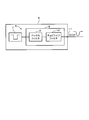
- FIG. 1 is a configuration diagram schematically showing a communication system in the first embodiment.
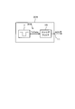
- FIG. 2 is a block diagram schematically showing the electrical configuration of the signal output device
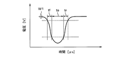
- FIG. 3 is an explanatory diagram of the regulations regarding falling pulses.
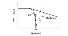
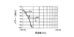
- FIG. 4 is an explanatory diagram of the regulation regarding the limit value of the radiated disturbance
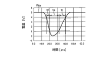
- FIG. 5 is an example of an output waveform when a falling pulse is input.
- FIG. 6 is a diagram schematically showing a simulation result related to a radiated disturbance wave
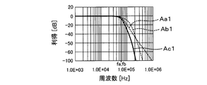
- FIG. 7 is a diagram schematically showing the frequency characteristics of the gain of each filter when the cutoff frequency of the first filter and the second filter is 1: 1.
- FIG. 8 is an example of an output waveform when a falling pulse is input when the cutoff frequency of the first filter and the second filter is 1: 1.
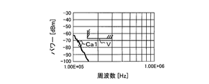
- FIG. 9 is a diagram schematically showing simulation results regarding pass characteristics and cutoff characteristics when the cutoff frequency of the first filter and the second filter is 1: 1.
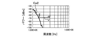
- FIG. 10 is a diagram schematically showing the frequency characteristics of the gain of each filter when the relationship between the cut-off frequencies of the first filter and the second filter is 1: x (where x is greater than 1 and less than or equal to 2.5).
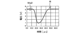
- FIG. 11 shows an output waveform example when a falling pulse is input when the relationship between the cut-off frequencies of the first filter and the second filter is 1: x (where x is greater than 1 and less than or equal to 2.5). Yes, FIG.
- FIG. 12 schematically shows simulation results regarding pass characteristics and cutoff characteristics when the relationship between the cutoff frequencies of the first filter and the second filter is 1: x (where x is greater than 1 and less than or equal to 2.5).
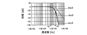
- FIG. FIG. 13 is a diagram schematically showing the frequency characteristics of the gain of each filter when the relationship between the cut-off frequencies of the first filter and the second filter is 1: y (where y is a predetermined value exceeding 2.5).
- FIG. 14 is an example of an output waveform when a falling pulse is input when the cutoff frequency of the first filter and the second filter is 1: y (where y is a predetermined value exceeding 2.5).
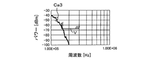
- FIG. 15 is a diagram schematically showing simulation results regarding pass characteristics and cutoff characteristics when the cutoff frequency of the first filter and the second filter is 1: y (where y is a predetermined value exceeding 2.5).
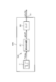
- FIG. 16 is a block diagram schematically showing the electrical configuration of the signal output device in the second embodiment.
- FIG. 17 is an example of an output waveform when a falling pulse is input.
- FIG. 18 is a diagram schematically showing a simulation result relating to the passage characteristic and the cutoff characteristic
- FIG. 19 is a block diagram schematically showing the electrical configuration of the signal output device in the third embodiment.
- FIG. 20 is a timing chart schematically showing signal changes at each node.
- FIG. 21 is a block diagram schematically showing the electrical configuration of the signal output device in the fourth embodiment.
- FIG. 22 is a timing chart schematically showing signal changes at each node.
- FIG. 23 is a block diagram schematically showing an electrical configuration of the signal output device in the fifth embodiment.
- FIG. 24 is a timing chart schematically showing signal changes at each node.
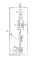
- FIG. 25 is a block diagram schematically showing the electrical configuration of the signal output apparatus in the sixth embodiment.
- FIG. 1 schematically shows the configuration of a communication system 1 in a vehicle.
- a communication device 2 and a communication device 3 are connected by a single line 4 as a transmission line.
- These communication devices 2 and 3 establish a master-slave relationship, and send and receive information through the single line 4. To do.
- the communication device 2 includes a signal output device 5 that shapes and outputs a rectangular signal, and a communication signal based on the output signal of the signal output device 5 is transmitted to the single line 4 so that the signal is transmitted to an in-vehicle network (not shown). Is output.
- harmonics corresponding to the communication signal are generated from the single line 4 and various noises corresponding to the harmonics are radiated to the outside together with the fundamental wave of the carrier of the communication signal.
- the signal output device 5 is configured as shown in FIG.
- the signal output device 5 includes a signal generator 7 and a filter unit 8 as the signal output unit 6.
- the signal generator 7 is a device for generating a communication signal, and generates a rectangular signal.
- the filter unit 8 includes a Bessel filter 9 as a first filter and a Chebyshev filter 10 as a second filter.
- the Bessel filter 9 is a 10th-order Bessel low-pass filter, for example, and can make the group delay characteristic flat as much as possible.
- the Bessel filter 9 is desirably set to a predetermined frequency of, for example, 150 [kHz] or less as a cutoff frequency.
- the Bessel filter 9 performs a low-pass filter process on the rectangular signal generated by the signal generator 7 and outputs it to the Chebyshev filter 10.
- the Chebyshev filter 10 is, for example, a fourth-order Chebyshev low-pass filter and can have an excellent cutoff characteristic. It is desirable that the Chebyshev filter 10 is also set with a predetermined frequency of 150 [kHz] or less as the cut-off frequency fb.
- the Chebyshev filter 10 performs a low-pass filter process on the rectangular signal generated by the Bessel filter 9 and outputs an analog signal AOUT from the output terminal 11.
- FIG. 2 of the present embodiment an example is shown in which the Bessel filter 9 is configured in the previous stage and the Chebyshev filter 10 is configured in the subsequent stage, but these may be provided in reverse.
- the Chebyshev filter 10 may be configured in the previous stage and the Bessel filter 9 may be configured in the subsequent stage.
- the filter unit 8 can reduce the waveform distortion and suppress harmonics by combining these two filter characteristics to blunt the rectangular signal. The details of the standard and the experimental results will be described below.
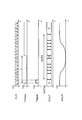
- FIG. 3 is an explanatory diagram for explaining the definition of a falling pulse in SENT (Single-Edge Nibble Transmission), and schematically shows a signal waveform W1 output for the falling single pulse.
- SENT is defined as a unidirectional / single wire communication protocol based on SAEJ2716 Single-Edge Nibble Transmission for Automotive Applications. This protocol is a protocol used for point-to-point transmission processing of signal values, and enables high-resolution data transfer.
- the falling time tf of the signal waveform W1 is less than 6.5 [ ⁇ s]
- the rising edge It is specified that the time tr is 18 [ ⁇ s] or less. Further, it is specified that the signal stabilization time ts is 6 [ ⁇ s] or more.
- the recommended limit value of the interference wave for protection of such an in-vehicle receiver is specified in the standard CISPR25 (1995) “In-vehicle”. It is stipulated in “Limits and Measurement Methods for Interference Waves for Receiver Protection”. As shown in the range of the standard value V in FIG. 4, according to this standard, specifications regarding the measurement of radiated disturbance waves in a frequency band of 150 [kHz] or more are defined.
- the frequency characteristic C1 of the waveform of a general rectangular signal is shown in FIG. 4, but in this rule, as shown in FIG. 4, in the LW band frequency band of 150 [kHz] or higher, 21 [dB ⁇ V / m].
- FIG. 5 schematically shows signal waveforms when the configuration of this embodiment is applied, corresponding to FIG. 3, and FIG. 6 shows output characteristics according to frequency changes when the configuration of this embodiment is applied. It is shown schematically corresponding to. It was confirmed that the SENT standard can be cleared by using the configuration of the present embodiment, as shown in the signal waveform Wa in FIG. Further, as shown in FIG. 6 showing the pass characteristic and the cutoff characteristic Ca, it was confirmed that the standard value V of the CISPR25 standard can be satisfied in a frequency band of 150 [kHz] or higher.
- the cutoff frequencies fa and fb of the Bessel filter 9 and the Chebyshev filter 10 have a better relationship.
- the Chebyshev filter 10 is superior in blocking characteristics than the Bessel filter 9. For this reason, it is preferable to set the cutoff frequency fa of the Bessel filter 9 to be equal to or lower than the cutoff frequency fb of the Chebyshev filter 10 and to further improve the cutoff characteristic at the cutoff frequency fb of the Chebyshev filter 10.
- FIGS. 7 to 9 show characteristic examples when the relationship between the cutoff frequencies fa and fb is 1: 1, and FIGS. 10 to 12 show the relationship between the cutoff frequencies fa and fb at 1: x (where x is 1).
- FIG. 13 to FIG. 15 show the case where the relationship between the cut-off frequencies fa and fb is 1: y (where y is a predetermined value exceeding 2.5).
- An example of the characteristic is schematically shown.
- 7 to 15 show characteristic examples when the cut-off frequency fb of the Chebyshev filter 10 is changed, for example, when the cut-off frequency fa of the Bessel filter 9 is 60 [kHz].
- An example is shown.
- FIG. 7 shows the characteristic of the Bessel filter 9, the frequency characteristic Ab1 shows the characteristic of the Chebyshev filter 10, and the frequency characteristic Ac1 shows their combined characteristics.
- the cutoff frequency fa: fb has a relationship of 1: 1
- the pass characteristic and the cutoff characteristic Ca1 sufficiently satisfy the standard value V as shown in FIG.
- ringing R occurs at the rising timing of the signal waveform Wa1 corresponding to a single pulse, and the ringing R exceeds a predetermined ratio (for example, 0.5%) with respect to the amplitude of the pulse. It turned out to be. There is a concern that the noise margin is reduced by the ringing R.
- the frequency characteristic Aa3 shown in FIG. 13 shows the characteristic of the Bessel filter 9
- the frequency characteristic Ab3 shows the characteristic of the Chebyshev filter 10
- the frequency characteristic Ac3 shows their combined characteristics.
- the cutoff frequency fa: fb has a relationship of 1: y
- the ringing R can be suppressed to a very small amount as shown in the signal waveform Wa3 in FIG.
- the pass characteristic and the cutoff characteristic Ca3 are insufficient and the standard cannot be satisfied.
- the cut-off frequency fa: fb satisfy the relationship of 1: x.
- the frequency characteristic Aa2 shown in FIG. 10 shows the characteristic of the Bessel filter 9, the frequency characteristic Ab2 shows the characteristic of the Chebyshev filter 10, and the frequency characteristic Ac2 shows their combined characteristics.
- the signal waveform Wa2 of FIG. 11 it is confirmed that the ringing R can be suppressed to a very small amount, and the pass characteristic and the cutoff characteristic Ca2 can sufficiently satisfy the standard value V as shown in FIG. It was. That is, it is desirable that the ratio between the cutoff frequency fa of the Bessel filter 9 and the cutoff frequency fb of the Chebyshev filter 10 is set to be more than 1: 1 and not more than 1: 2.5.
- the ratio of the cutoff frequency fa of the Bessel filter 9 and the cutoff frequency fb of the Chebyshev filter 10 is set to exceed 1: 1 and 1: 2.5 or less.
- the cut-off frequency fa of the Bessel filter 9 or the cut-off frequency fb of the Chebyshev filter 10 is preferably set to 150 [kHz] or less, and at this time, it is possible to easily satisfy the regulations regarding in-vehicle noise.
- the cutoff frequency of the filter unit 8 is desirably 4 times or less the reciprocal of the minimum pulse interval used in the communication device 2. Further, it is desirable that the cutoff frequency of the filter unit 8 is not more than twice the frequency calculated from the slew rate used for the communication device 2.
- the signal output unit 6 outputs a signal obtained through the pass characteristics of the Bessel filter 9 and the Chebyshev filter 10 for the rectangular signal. Can be dulled.
- the cutoff frequency fa of the Bessel filter 9 is set lower than the cutoff frequency fb of the Chebyshev filter 10, the ringing R can be suppressed so as to satisfy a desired condition while enabling a desired frequency band limitation.
- the communication standard in SENT can be cleared and the standard of CISPR25 can be satisfied.
- FIGS. 16 to 18 show additional explanatory views of the second embodiment.
- FIG. 16 shows an alternative configuration to FIG. 2, and
- FIGS. 17 and 18 show characteristic diagrams corresponding to FIGS. 5 and 6, respectively.
- the signal output device 105 in place of the signal output device 5 includes a signal generator 7 and a filter unit 108 as the signal output device 106.
- the filter unit 108 according to the present embodiment includes the Bessel filter 9 as the first filter and the Butterworth filter 12 as the second filter.
- the Butterworth filter 12 is, for example, a fourth-order Butterworth low-pass filter, and can have excellent cutoff characteristics.
- the Butterworth filter 12 can set, for example, a predetermined frequency of 150 [kHz] or less as the cutoff frequency fc.
- the Butterworth filter 12 performs a low-pass filter process on the rectangular signal generated by the Bessel filter 9 and outputs it as an analog signal AOUT from the output terminal 11.
- FIG. 16 of the present embodiment an example is shown in which the Bessel filter 9 is configured in the previous stage and the Butterworth filter 12 is configured in the subsequent stage, but these may be provided in reverse. That is, the Butterworth filter 12 may be configured in the previous stage and the Bessel filter 9 may be configured in the subsequent stage.
- the filter unit 108 can reduce the waveform distortion and suppress the harmonics by combining these two filter characteristics to blunt the rectangular signal.
- FIG. 17 schematically shows the signal waveform W2 when the configuration of the present embodiment is applied, corresponding to FIG. 3, and FIG. 18 shows the output characteristics according to the frequency change when the configuration of the present embodiment is applied. 4 schematically.
- the filter unit 108 is configured by combining the Bessel filter 9 and the Butterworth filter 12, and the rectangular signal generated by the signal generator 7 is output through the filter unit 108. I made it. Further, since the cutoff frequency fa of the Bessel filter 9 is set lower than the cutoff frequency fb of the Butterworth filter 12, ringing can be suppressed so as to satisfy a desired condition while enabling a desired frequency band limitation. In particular, the CISPR25 standard can be satisfied.
- FIG. 19 and 20 show additional explanatory views of the third embodiment.
- the filter units 8 and 108 are not used is shown.
- FIG. 19 schematically shows the configuration of the signal output device 205.
- the signal output device 205 includes a transmission signal generator 13, an edge detection circuit 14, a memory control circuit 15, and a D / A converter 16 as the signal output unit 206.
- the transmission signal generator 13 receives the clock signal CLK generated by the clock generator 17 and generates transmission data TxData having binary levels “H” and “L”.
- the edge detection circuit 14 receives the transmission data TxData from the transmission signal generator 13 and detects an edge (for example, a falling edge) of the transmission data TxData.
- the edge detection circuit 14 generates a trigger signal Trigger according to the detected edge and outputs it to the memory control circuit 15.
- the memory control circuit 15 includes a memory 15a such as a ROM as a storage unit.
- waveform data DATA corresponding to the transmission signal TxData of “L” level having a predetermined length L is stored in advance as parallel digital data.
- the waveform data DATA is data obtained by analog-digital conversion of the analog signal AOUT described in the first or second embodiment in advance with N bits (where N ⁇ 2) and expressed as a digital value.
- the memory control circuit 15 can output the waveform data DATA stored in the memory 15a in synchronization with the clock signal CLK using N-bit parallel data DOUT.
- the D / A converter 16 receives the N-bit parallel data DOUT output from the memory control circuit 15. When the D / A converter 16 receives the N-bit parallel data DOUT, the D / A converter 16 performs digital-analog conversion and outputs an analog signal AOUT from the output terminal 11.
- FIG. 20 is a schematic timing chart showing signal changes at each node.
- the transmission signal generator 19 outputs transmission data TxData having a predetermined length L in synchronization with the clock signal CLK.
- the edge detection circuit 14 outputs a trigger signal Trigger to the memory control circuit 15 when detecting the first edge (for example, falling edge) of the transmission data TxData.
- the memory control circuit 15 When receiving the trigger signal Trigger, the memory control circuit 15 outputs the waveform data DATA stored in advance in the memory 15a as parallel data DOUT.
- the waveform data DATA is a waveform obtained by digitally converting the analog signal AOUT output from the output terminal 11 described in the first or second embodiment in advance, the D / A converter 16 performs the digital conversion. If the data is digital-analog converted again, an analog signal AOUT corresponding to the predetermined length L can be output.
- ringing can be suppressed while realizing a desired frequency band limitation.
- the memory control circuit 15 outputs all of the waveform data DATA with one input trigger signal Trigger, and outputs an analog signal AOUT obtained by digital-analog conversion.
- the same operational effects as those of the above-described embodiment can be obtained, and the memory control circuit 15 can output the analog signal AOUT corresponding to the waveform data DATA only by receiving the trigger signal Trigger.
- the predetermined length L is shown, but a plurality of types may be provided.
- the memory control circuit 15 selects and outputs parallel data DOUT corresponding to a plurality of waveform data DATA having a predetermined length L from the memory 15a. Accordingly, different analog signals AOUT can be output corresponding to a plurality of transmission data TxData having a predetermined length L.
- FIG. 21 schematically shows the configuration of the signal output device 305.
- the signal output device 305 includes a signal generator 7 and an analog filter 18 as a signal output unit 306.
- the signal generator 7 generates a rectangular signal for communication.
- the analog filter 18 is an analog filter in which the Bessel filter 9 and the Chebyshev filter 10 are connected in cascade, and the characteristics are the same as in the first embodiment. For this reason, as schematically shown in the timing chart of FIG. 22, the analog signal AOUT that is the output of the analog filter 18 shows a signal waveform in which the transmission data TxData is blunted.
- the analog filter 18 may be configured to include the Bessel filter 9 and the Butterworth filter 12 as shown in the second embodiment.
- the characteristics in this case are the same as those in the second embodiment, and the same effects as those in the second embodiment are achieved.
- FIG. 23 schematically shows the configuration of the signal output device 405.
- the signal output device 405 includes a signal generator 7, a digital filter 19, and a D / A converter 20 as a signal output unit 406.
- the signal generator 7 generates a rectangular signal for communication.
- the digital filter 19 is composed of a digital circuit in which a Bessel filter 9 and a Chebyshev filter 10 are connected in cascade.
- the Bessel filter and the Chebyshev filter are configured by combining, for example, an IIR filter, an FIR filter, and the like. Also in this case, the characteristics are the same as in the first embodiment.
- the transmission data TxData is digitally filtered and output as parallel data DOUT.
- the parallel data DOUT is illustrated in FIG. 24 so that the transmission data TxData is output from the timing when it is input to the digital filter, the parallel data DOUT is substantially processed by the digital filter 19, so that the parallel data The output of DOUT is delayed by a predetermined number of clocks.
- the D / A converter 20 outputs an analog signal AOUT corresponding to the parallel data DOUT.
- the analog signal AOUT represents a signal waveform obtained by blunting the transmission data TxData, and has the same effect as that of the above-described embodiment.
- the digital filter 19 may be configured to include the Bessel filter 9 and the Butterworth filter 12 as shown in the second embodiment.
- the characteristics in this case are the same as those in the second embodiment, and the same effects as those in the second embodiment are achieved.
- FIG. 25 shows an additional explanatory diagram of the sixth embodiment.
- FIG. 25 schematically shows the configuration of the signal output device 505.
- a signal output device 505 shown in FIG. 25 includes a signal generator 7, a waveform shaping device 21, and an amplifier 22 as a signal output device 506.
- a waveform shaping device 21 is connected to the subsequent stage of the signal generator 7.
- the waveform shaping device 21 includes filter units 8 and 108 according to the first to third embodiments, an edge detection circuit 14 according to the fourth embodiment, a memory control circuit 15, a D / A converter 16, and an analog filter according to the fifth embodiment. 18.
- the digital filter 19 and the D / A converter 20 of the sixth embodiment can be applied.
- An amplifier 22 is connected to the subsequent stage of the waveform shaping device 21.
- the amplifier 22 amplifies the analog signal AOUT and outputs the analog signal AOUT2 from the output terminal 11. By providing the signal output unit 506 with the amplifier 22, the analog signal AOUT can be amplified and output.
- 4 is a single line
- 5, 105, 205, 305, 405, and 505 are signal output devices
- 6, 106, 206, 306, 406, and 506 are signal output devices
- 9 is a Bessel filter corresponding to the first filter.
- 10 is a Chebyshev filter equivalent to the second filter
- 12 is a Butterworth filter equivalent to the second filter
- 15a is a memory as a storage unit
- fa is a cutoff frequency of the Bessel filter
- fb is a cutoff frequency of the Chebyshev filter
- fc is Butterworth Indicates the cutoff frequency of the filter.
- the in-vehicle communication standard is not limited to SENT, and can be applied to a system adopting a standard such as LIN (Local Interconnect Network).
- LIN Local Interconnect Network
- a form using a rectangular signal has been shown, this is an example of a signal including harmonics, and the signal used for this communication may be a pulse, and a predetermined signal having an arbitrary waveform is used. It is possible.
- the form applied to vehicle mounting was mentioned, it is not restricted especially for vehicles.
Landscapes
- Engineering & Computer Science (AREA)
- Computer Networks & Wireless Communication (AREA)
- Signal Processing (AREA)
- Physics & Mathematics (AREA)
- Mathematical Physics (AREA)
- Computer Hardware Design (AREA)
- Algebra (AREA)
- General Physics & Mathematics (AREA)
- Pure & Applied Mathematics (AREA)
- Dc Digital Transmission (AREA)
- Filters And Equalizers (AREA)
- Cable Transmission Systems, Equalization Of Radio And Reduction Of Echo (AREA)
Abstract
信号出力装置(5、105、205、305、405、505)は、単線(4)を用いて他の通信機器(3)と通信する通信機器(2)に設けられる。信号出力器(6、106、206、306、406、506)は、任意の信号となる所定信号について、ベッセルフィルタによる第1フィルタ(9)、及びチェビシェフフィルタまたはバターワースフィルタによる第2フィルタ(10、12)の通過特性を介して得られる信号を出力する。前記第1フィルタのカットオフ周波数(fa)は前記第2フィルタのカットオフ周波数(fb、fc)より低く設定されている。
Description
本出願は、2016年1月14日に出願された日本特許出願番号2016-005237号に基づくもので、ここにその記載内容を援用する。
本開示は、伝送線路から放射されるノイズを低減しながら波形成形して出力する機能を備える信号出力装置に関する。
例えば、車両に搭載される複数の車載装置は伝送線路に信号を送信して互いに通信する。この通信信号は高調波を含んでいるため、伝送線路から高調波ノイズが放射される。このような高調波ノイズを抑制するため各種の放射ノイズ低減技術が開発されている(例えば、特許文献1参照)。特許文献1記載の発明によれば、矩形信号の帯域制限を行うことで放射ノイズを低減できる。
特許文献1記載の技術を用いたとしても、帯域制限をした波形にリンギングを生じてしまい、ノイズマージンがなくなることが懸念される。すなわちリンギングの発生を許容しない、又は、厳しい制約がある通信規格を採用したときには、特許文献1記載の技術を適用できないという問題を生じる。したがってリンギングを抑制しながら周波数帯域制限可能にした波形を出力することが望まれている。
本開示の目的は、所望の周波数帯域制限を可能にしつつリンギングを抑制できるようにした信号出力装置を提供することである。
本開示の一態様によれば、信号出力器が任意の波形となる所定信号についてベッセルフィルタによる第1フィルタ、及び、チェビシェフフィルタまたはバターワースフィルタによる第2フィルタの通過特性を介して得られる信号を出力するため、たとえ任意の波形が矩形信号であったとしてもこの矩形信号のエッジを鈍らせることができる。さらに、第1フィルタのカットオフ周波数が第2フィルタのカットオフ周波数より低く設定されているため、所望の周波数帯域制限を可能にしつつリンギングを抑制できる。
本開示の一態様によれば、信号出力器が任意の波形となる所定信号についてベッセルフィルタによる第1フィルタ、及び、チェビシェフフィルタまたはバターワースフィルタによる第2フィルタの通過特性を介して得られる信号を出力するため、たとえ任意の波形が矩形信号であったとしてもこの矩形信号のエッジを鈍らせることができる。さらに、第1フィルタのカットオフ周波数が第2フィルタのカットオフ周波数より低く設定されているため、所望の周波数帯域制限を可能にしつつリンギングを抑制できる。
本開示についての上記目的およびその他の目的、特徴や利点は、添付の図面を参照しながら下記の詳細な記述により、より明確になる。その図面は、
図1は、第1実施形態における通信システムを概略的に示す構成図であり、
図2は、信号出力装置の電気的構成を概略的に示すブロック図であり、
図3は、立下りパルスに関する規定の説明図であり、
図4は、放射妨害波の限度値に関する規定の説明図であり、
図5は、立下りパルスを入力したときの出力波形例であり、
図6は、放射妨害波に関するシミュレーション結果を概略的に示す図であり、
図7は、第1フィルタと第2フィルタのカットオフ周波数が1:1となるときの各フィルタの利得の周波数特性を概略的に示す図であり、
図8は、第1フィルタと第2フィルタのカットオフ周波数が1:1となるときに、立下りパルスを入力したときの出力波形例であり、
図9は、第1フィルタと第2フィルタのカットオフ周波数が1:1となるときの、通過特性、遮断特性に関するシミュレーション結果を概略的に示す図であり、
図10は、第1フィルタと第2フィルタのカットオフ周波数の関係が1:x(但しxは1を超え2.5以下)となるときの各フィルタの利得の周波数特性を概略的に示す図であり、
図11は、第1フィルタと第2フィルタのカットオフ周波数の関係が1:x(但しxは1を超え2.5以下)となるときに、立下りパルスを入力したときの出力波形例であり、
図12は、第1フィルタと第2フィルタのカットオフ周波数の関係が1:x(但しxは1を超え2.5以下)となるときの、通過特性、遮断特性に関するシミュレーション結果を概略的に示す図であり、
図13は、第1フィルタと第2フィルタのカットオフ周波数の関係が1:y(但しyは2.5を超える所定値)となるときの各フィルタの利得の周波数特性を概略的に示す図であり、
図14は、第1フィルタと第2フィルタのカットオフ周波数が1:y(但しyは2.5を超える所定値)となるときに、立下りパルスを入力したときの出力波形例であり、
図15は、第1フィルタと第2フィルタのカットオフ周波数が1:y(但しyは2.5を超える所定値)となるときの、通過特性、遮断特性に関するシミュレーション結果を概略的に示す図であり、
図16は、第2実施形態において信号出力装置の電気的構成を概略的に示すブロック図であり、
図17は、立下りパルスを入力したときの出力波形例であり、
図18は、通過特性、遮断特性に関するシミュレーション結果を概略的に示す図であり、
図19は、第3実施形態において信号出力装置の電気的構成を概略的に示すブロック図であり、
図20は、各ノードの信号変化を概略的に示すタイミングチャートであり、
図21は、第4実施形態において信号出力装置の電気的構成を概略的に示すブロック図であり、
図22は、各ノードの信号変化を概略的に示すタイミングチャートであり、
図23は、第5実施形態において信号出力装置の電気的構成を概略的に示すブロック図であり、
図24は、各ノードの信号変化を概略的に示すタイミングチャートであり、
図25は、第6実施形態において信号出力装置の電気的構成を概略的に示すブロック図である。
以下、信号出力装置の幾つかの実施形態について図面を参照しながら説明する。以下に説明する各実施形態において、同一又は類似の動作を行う構成については、同一又は類似の符号を付している。
(第1実施形態)
図1から図15は第1実施形態の説明図を概略的に示している。図1は車両内の通信システム1の構成を概略的に示している。この通信システム1は、通信機器2と通信機器3とが伝送線路としての単線4により接続されており、これらの通信機器2及び3がマスタ-スレーブの関係を構築し、単線4を通じて情報を送受信する。
図1から図15は第1実施形態の説明図を概略的に示している。図1は車両内の通信システム1の構成を概略的に示している。この通信システム1は、通信機器2と通信機器3とが伝送線路としての単線4により接続されており、これらの通信機器2及び3がマスタ-スレーブの関係を構築し、単線4を通じて情報を送受信する。
通信機器2は、矩形信号を波形成形して出力する信号出力装置5を備えており、この信号出力装置5の出力信号に基づく通信信号が単線4に伝達され、信号が図示しない車両内ネットワークに出力される。単線4から通信信号に応じた高調波を生じ、当該通信信号のキャリアの基本波と共に高調波に応じた様々なノイズを外部に放射する虞がある。
そこで、本実施形態では、信号出力装置5を図2に示すように構成している。図2に示すように、この信号出力装置5は、信号出力器6として、信号生成器7とフィルタ部8とを備える。信号生成器7は、通信用信号を生成するための機器であり、矩形信号を生成する。フィルタ部8は、第1フィルタとしてベッセルフィルタ9を備え、第2フィルタとしてチェビシェフフィルタ10を備えている。ベッセルフィルタ9は、例えば10次のベッセルローパスフィルタであり群遅延特性を最大限平坦とすることができる。このベッセルフィルタ9は例えば150[kHz]以下の所定周波数をカットオフ周波数として設定されていることが望ましい。このベッセルフィルタ9は、信号生成器7により生成される矩形信号をローパスフィルタ処理し、チェビシェフフィルタ10に出力する。
またチェビシェフフィルタ10は、例えば4次のチェビシェフローパスフィルタであり遮断特性を優れたものにできる。このチェビシェフフィルタ10もまた例えば150[kHz]以下の所定周波数をカットオフ周波数fbとして設定されていることが望ましい。このチェビシェフフィルタ10は、ベッセルフィルタ9により生成される矩形信号をローパスフィルタ処理し、出力端子11からアナログ信号AOUTを出力する。本実施形態の図2の構成では、ベッセルフィルタ9を前段に構成しチェビシェフフィルタ10を後段に構成した例を示しているが、これらは逆に設けても良い。すなわちチェビシェフフィルタ10を前段に構成しベッセルフィルタ9を後段に構成しても良い。フィルタ部8は、これらの2つのフィルタ特性を組み合わせて矩形信号を鈍らせることで波形歪を少なくできると共に高調波を抑制できる。以下、規格の詳細とその実験結果を説明する。
図3はSENT(Single-Edge Nibble Transmission)における立下りパルスの規定を説明する説明図を示しており、立下り単パルスに対して出力される信号波形W1を概略的に示している。SENTはSAEJ2716のSingle-Edge Nibble Transmission for Automotive Applicationsに基づく単方向/単線式通信プロトコルとして規定されている。このプロトコルは、信号値のポイントツーポイントの送信処理に用いられるプロトコルであり、高分解能のデータ転送を可能にする。
図3に示すように、このSENTの規格上では、立下りパルスを発生したときに、その信号波形W1の立下り時間tfを6.5[μs]未満とすることが規定されると共に、立上り時間trを18[μs]以下とすることが規定されている。また、信号安定時間tsを6[μs]以上とすることが規定されている。
また、車両はAMラジオ、FMラジオなどを受信するための受信機を搭載しているため、このような車載受信機の保護のための妨害波の推奨限度値などが規格CISPR25(1995)「車載受信機保護のための妨害波の限度値及び測定法」に定められている。図4に規格値Vの範囲を示すように、この規格によれば、150[kHz]以上の周波数帯域における放射妨害波測定に関する仕様が規定されている。一般的な矩形信号の波形の周波数特性C1を図4中に示しているが、この規定では、図4中に示すように、150[kHz]以上のLW帯の周波数帯域において、21[dBμV/m]未満とするように規定されている。
図5は本実施形態の構成を適用したときの信号波形を図3に対応して概略的に示し、図6は本実施形態の構成を適用したときの周波数変化に応じた出力特性を図4に対応して概略的に示している。本実施形態の構成を用いることで、図5に信号波形Waを示すように、SENTの規格をクリアできることが確認された。また、図6に通過特性、遮断特性Caを示すように、150[kHz]以上の周波数帯域において、CISPR25規格の規格値Vを満たすことができることが確認された。
以下、フィルタ部8を適用したときに、ベッセルフィルタ9とチェビシェフフィルタ10のカットオフ周波数fa、fbがより良い関係性となることについて説明する。チェビシェフフィルタ10はベッセルフィルタ9より遮断特性に優れている。このため、ベッセルフィルタ9のカットオフ周波数faをチェビシェフフィルタ10のカットオフ周波数fb以下に設定し、チェビシェフフィルタ10のカットオフ周波数fbにおいて遮断特性をより高めると良い。
図7から図9はカットオフ周波数faとfbとの関係を1:1とした場合の特性例、図10から図12はカットオフ周波数faとfbとの関係を1:x(但しxは1を超え2.5以下)とした場合の特性例を示し、図13から図15はカットオフ周波数faとfbとの関係を1:y(但しyは2.5を超える所定値)とした場合の特性例を概略的に示している。これらの図7から図15は、例えばベッセルフィルタ9のカットオフ周波数fa=60[kHz]とした場合、チェビシェフフィルタ10のカットオフ周波数fbを変更したときの特性例を示している。例えば、図7~図9はfb=60[kHz]、図10~図12はfb=100[kHz]、図13~図15はfb=151[kHz](すなわち>150[kHz])の特性例を示している。
図7に示す周波数特性Aa1はベッセルフィルタ9の特性を示し、周波数特性Ab1はチェビシェフフィルタ10の特性を示し、周波数特性Ac1はこれらの合成特性を示している。図7から図9に示すように、カットオフ周波数fa:fbが1:1の関係性を備えるときには、図9に示すように、通過特性、遮断特性Ca1は十分に規格値Vを満たすことがわかるが、図8に示すように、単パルスに応じた信号波形Wa1の立上りタイミングにおいてリンギングRを生じてしまい、パルスの振幅に対し所定割合(例えば0.5%)を超えるリンギングRを生じてしまうことが判明した。このリンギングRによってノイズマージンが減少することが懸念される。
また、図13に示す周波数特性Aa3はベッセルフィルタ9の特性を示し、周波数特性Ab3はチェビシェフフィルタ10の特性を示し、周波数特性Ac3はこれらの合成特性を示している。図13から図15に示すように、カットオフ周波数fa:fbが1:yの関係性を備えるときには、図14に信号波形Wa3を示すように、リンギングRはごく少量に抑えることができることが確認されたが、図15に示すように、通過特性、遮断特性Ca3は不十分であり規格を満たすことができないことが判明した。
このため、図10から図12に示すように、カットオフ周波数fa:fbが1:xの関係を満たすように構成することが望ましい。図10に示す周波数特性Aa2はベッセルフィルタ9の特性を示し、周波数特性Ab2はチェビシェフフィルタ10の特性を示し、周波数特性Ac2はこれらの合成特性を示している。図11の信号波形Wa2に示すように、リンギングRをごく少量に抑えることができると共に、図12に示すように、通過特性、遮断特性Ca2も十分に規格値Vを満たすことができることが確認された。すなわち、ベッセルフィルタ9のカットオフ周波数faとチェビシェフフィルタ10のカットオフ周波数fbとの比が1対1を超え且つ1対2.5以下に設定されていることが望ましい。
本実施形態によれば、ベッセルフィルタ9のカットオフ周波数faとチェビシェフフィルタ10のカットオフ周波数fbとの比が1:1を超え且つ1:2.5以下に設定されているときに、より良好な特性にすることができる。ベッセルフィルタ9のカットオフ周波数fa又はチェビシェフフィルタ10のカットオフ周波数fbは150[kHz]以下に設定されていることが望ましく、このとき車載ノイズに関する規定を容易に満たすことができる。
より望ましくは、フィルタ部8のカットオフ周波数を、通信機器2に用いられる最小パルス間隔の逆数の4倍以下とすることが望ましい。また、フィルタ部8のカットオフ周波数は通信機器2に用いられるスルーレートから算出された周波数の2倍以下とすることが望ましい。
以上説明したように、本実施形態によれば、信号出力器6が矩形信号についてベッセルフィルタ9及びチェビシェフフィルタ10の通過特性を介して得られる信号を出力するため、この単パルスの信号のエッジを鈍らせることができる。このときベッセルフィルタ9のカットオフ周波数faがチェビシェフフィルタ10のカットオフ周波数fbより低く設定されているため、所望の周波数帯域制限を可能にしつつ所望の条件を満たすようにリンギングRを抑制できる。特に本実施形態によれば、SENTにおける通信規格をクリアできると共に、CISPR25の規格を満たすようにすることが可能となる。
(第2実施形態)
図16から図18は第2実施形態の追加説明図を示す。図16は図2に代わる構成を示しており、図17、図18は、それぞれ図5、図6に対応した特性図を示している。
図16から図18は第2実施形態の追加説明図を示す。図16は図2に代わる構成を示しており、図17、図18は、それぞれ図5、図6に対応した特性図を示している。
図16に示すように、信号出力装置5に代わる信号出力装置105は、信号出力器106として、信号生成器7とフィルタ部108とを備えている。本実施形態に係るフィルタ部108は、第1フィルタとしてベッセルフィルタ9を備え、第2フィルタとしてバターワースフィルタ12を備えている。
ベッセルフィルタ9は第1実施形態と同様の構成であるため説明を省略する。またバターワースフィルタ12は、例えば4次のバターワースローパスフィルタであり遮断特性を優れた特性とすることができる。このバターワースフィルタ12は例えば150[kHz]以下の所定周波数をカットオフ周波数fcとして設定できる。このバターワースフィルタ12は、ベッセルフィルタ9により生成される矩形信号をローパスフィルタ処理し、出力端子11からアナログ信号AOUTとして出力する。本実施形態の図16の構成では、ベッセルフィルタ9を前段に構成しバターワースフィルタ12を後段に構成した例を示しているが、これらは逆に設けても良い。すなわちバターワースフィルタ12を前段に構成しベッセルフィルタ9を後段に構成しても良い。フィルタ部108は、これらの2つのフィルタ特性を組み合わせて矩形信号を鈍らせることで波形歪を少なくできると共に高調波を抑制できる。
図17は本実施形態の構成を適用したときの信号波形W2を図3に対応して概略的に示し、図18は本実施形態の構成を適用したときの周波数変化に応じた出力特性を図4に対応して概略的に示している。本実施形態の構成を用いることで、図17に信号波形Wbを示すように、立下りパルスの応答に関する規格を満たすようにできることが確認された。また、図18に周波数特性Cbを示すように、150[kHz]以上の周波数帯域において、規格CISPR25を満たすことが確認された。また、第1実施形態と同様に、カットオフ周波数faをカットオフ周波数fcより低く設定することで、所望の周波数帯域制限を可能にしつつ所望の条件を満たすようにリンギングを抑制できることが確認されている。
以上説明したように、本実施形態では、ベッセルフィルタ9とバターワースフィルタ12とを組み合わせてフィルタ部108を構成し、信号生成器7により生成される矩形信号についてフィルタ部108を通過して出力するようにした。また、ベッセルフィルタ9のカットオフ周波数faをバターワースフィルタ12のカットオフ周波数fbより低く設定したので、所望の周波数帯域制限を可能にしつつ所望の条件を満たすようにリンギングを抑制できる。特に、CISPR25の規格を満たすことができる。
(第3実施形態)
図19および図20は第3実施形態の追加説明図を示す。この第3実施形態では、フィルタ部8、108を用いることなく構成した例を示す。
図19および図20は第3実施形態の追加説明図を示す。この第3実施形態では、フィルタ部8、108を用いることなく構成した例を示す。
図19は信号出力装置205の構成を概略的に示している。図19に示すように、信号出力装置205は、信号出力器206として、送信信号生成器13、エッジ検出回路14、メモリ制御回路15、及び、D/Aコンバータ16を備える。送信信号生成器13は、クロック生成器17により生成されるクロック信号CLKを入力し2値レベル「H」「L」の送信データTxDataを生成する。
エッジ検出回路14は、送信信号生成器13の送信データTxDataを入力し、この送信データTxDataのエッジ(例えば立下りエッジ)を検出する。エッジ検出回路14は、検出されたエッジに応じてトリガ信号Triggerを発生しメモリ制御回路15に出力する。メモリ制御回路15は、ROMなどのメモリ15aを記憶部として備える。メモリ15aには、所定長Lの「L」レベルの送信信号TxDataに対応した波形データDATAがパラレルデジタルデータとして予め記憶されている。この波形データDATAは、第1又は第2実施形態にて説明したアナログ信号AOUTを、予めNビット(但しN≧2)でアナログデジタル変換してデジタル値として表したデータである。
メモリ制御回路15は、メモリ15aに記憶された波形データDATAを、NビットのパラレルデータDOUTによりクロック信号CLKに同期出力可能になっている。D/Aコンバータ16は、このメモリ制御回路15から出力されたNビットのパラレルデータDOUTを入力する。D/Aコンバータ16はこのNビットのパラレルデータDOUTを入力すると、デジタルアナログ変換し、出力端子11からアナログ信号AOUTを出力する。
図20は各ノードの信号変化について概略的なタイミングチャートにより示している。送信信号生成器19はクロック信号CLKに同期して所定長Lの送信データTxDataを出力する。エッジ検出回路14はこの送信データTxDataの初回のエッジ(例えば立下りエッジ)を検出すると、トリガ信号Triggerをメモリ制御回路15に出力する。メモリ制御回路15はこのトリガ信号Triggerを受付けると、メモリ15aに予め記憶されている波形データDATAをパラレルデータDOUTとして出力する。前述したように、この波形データDATAは、第1又は第2実施形態で説明した出力端子11から出力されるアナログ信号AOUTを予めデジタル変換処理した波形であるため、D/Aコンバータ16がこのデジタルデータを再度デジタルアナログ変換すれば、所定長Lに対応したアナログ信号AOUTを出力できる。このように本実施形態の構成を適用したときにおいても、所望の周波数帯域制限を実現しつつリンギングを抑制できる。
本実施形態によれば、メモリ制御回路15は入力される1つのトリガ信号Triggerで波形データDATAのすべてを出力し、デジタルアナログ変換したアナログ信号AOUTを出力するようにした。これにより、前述実施形態と同様の作用効果を得ることができると共に、メモリ制御回路15はトリガ信号Triggerを受け付けるだけで波形データDATAに対応したアナログ信号AOUTを出力できる。
前述では、所定長Lを1種類だけ示したが複数種類設けても良い。この場合、メモリ15aには、複数の所定長Lに対応した複数の波形データDATAを予め記憶させておくことが望ましい。この場合、メモリ制御回路15はトリガ信号Triggerを入力すると複数の所定長Lの複数の波形データDATAに対応したパラレルデータDOUTをメモリ15aから選択して出力する。これにより、複数の所定長Lの送信データTxDataに対応して互いに異なるアナログ信号AOUTを出力できる。
(第4実施形態)
図21および図22は第4実施形態の追加説明図を示す。第4実施形態ではアナログフィルタ18を用いた構成例を示す。図21は信号出力装置305の構成を概略的に示している。図21に示すように、信号出力装置305は、信号出力器306として、信号生成器7とアナログフィルタ18とを備える。信号生成器7は、通信するための矩形信号を生成する。アナログフィルタ18はベッセルフィルタ9とチェビシェフフィルタ10とを縦続接続したアナログフィルタであり、特性は第1実施形態と同様である。このため図22にタイミングチャートを概略的に示すように、アナログフィルタ18の出力となるアナログ信号AOUTは、送信データTxDataを鈍らせた信号波形を示すことになる。これにより第1実施形態と同様の作用効果を奏する。また、アナログフィルタ18を、第2実施形態に示したようにベッセルフィルタ9とバターワースフィルタ12とを備えた構成としても良い。この場合の特性は第2実施形態と同様となり、第2実施形態と同様の作用効果を奏する。
図21および図22は第4実施形態の追加説明図を示す。第4実施形態ではアナログフィルタ18を用いた構成例を示す。図21は信号出力装置305の構成を概略的に示している。図21に示すように、信号出力装置305は、信号出力器306として、信号生成器7とアナログフィルタ18とを備える。信号生成器7は、通信するための矩形信号を生成する。アナログフィルタ18はベッセルフィルタ9とチェビシェフフィルタ10とを縦続接続したアナログフィルタであり、特性は第1実施形態と同様である。このため図22にタイミングチャートを概略的に示すように、アナログフィルタ18の出力となるアナログ信号AOUTは、送信データTxDataを鈍らせた信号波形を示すことになる。これにより第1実施形態と同様の作用効果を奏する。また、アナログフィルタ18を、第2実施形態に示したようにベッセルフィルタ9とバターワースフィルタ12とを備えた構成としても良い。この場合の特性は第2実施形態と同様となり、第2実施形態と同様の作用効果を奏する。
(第5実施形態)
図23および図24は第5実施形態の追加説明図を示す。第5実施形態においては、フィルタ部としてデジタルフィルタ19を用いた構成例を示す。図23は信号出力装置405の構成を概略的に示している。図23に示すように、信号出力装置405は、信号出力器406として、信号生成器7とデジタルフィルタ19とD/Aコンバータ20とを備える。信号生成器7は、通信するための矩形信号を生成する。デジタルフィルタ19はベッセルフィルタ9とチェビシェフフィルタ10とを縦続接続したデジタル回路により構成されている。本実施形態では、ベッセルフィルタ、チェビシェフフィルタは例えばIIRフィルタ、FIRフィルタなどを組み合わせて構成される。この場合も特性は第1実施形態と同様である。
図23および図24は第5実施形態の追加説明図を示す。第5実施形態においては、フィルタ部としてデジタルフィルタ19を用いた構成例を示す。図23は信号出力装置405の構成を概略的に示している。図23に示すように、信号出力装置405は、信号出力器406として、信号生成器7とデジタルフィルタ19とD/Aコンバータ20とを備える。信号生成器7は、通信するための矩形信号を生成する。デジタルフィルタ19はベッセルフィルタ9とチェビシェフフィルタ10とを縦続接続したデジタル回路により構成されている。本実施形態では、ベッセルフィルタ、チェビシェフフィルタは例えばIIRフィルタ、FIRフィルタなどを組み合わせて構成される。この場合も特性は第1実施形態と同様である。
このため、図24にタイミングチャートを概略的に示すように、デジタルフィルタ19が所定長Lの送信データTxDataを入力すると、この送信データTxDataをデジタルフィルタ処理しパラレルデータDOUTとして出力する。なお、パラレルデータDOUTは、送信データTxDataがデジタルフィルタに入力されたタイミングから出力されるように図24には図示しているが、実質的にはデジタルフィルタ19により処理が行われるため、パラレルデータDOUTの出力は所定クロック数分だけ遅延することになる。D/Aコンバータ20は、このパラレルデータDOUTを入力すると、このパラレルデータDOUTに対応したアナログ信号AOUTを出力する。アナログ信号AOUTは、送信データTxDataを鈍らせた信号波形を表すことになり、前述の実施形態と同様の作用効果を奏する。
また、デジタルフィルタ19を、第2実施形態に示したようにベッセルフィルタ9及びバターワースフィルタ12を備えた構成としても良い。この場合の特性は第2実施形態と同様となり、第2実施形態と同様の作用効果を奏する。
(第6実施形態)
図25は第6実施形態の追加説明図を示す。図25は信号出力装置505の構成を概略的に示している。図25に示す信号出力装置505は、信号出力器506として、信号生成器7と波形成形装置21とアンプ22とを備えている。信号生成器7の後段には波形成形装置21が接続されている。波形成形装置21は、第1から第3実施形態のフィルタ部8、108、第4実施形態のエッジ検出回路14、メモリ制御回路15、及び、D/Aコンバータ16、第5実施形態のアナログフィルタ18、第6実施形態のデジタルフィルタ19及びD/Aコンバータ20、を適用できる。この波形成形装置21の後段にはアンプ22が接続されている。アンプ22は、アナログ信号AOUTを増幅し、出力端子11からアナログ信号AOUT2を出力する。信号出力器506にアンプ22を設けることでアナログ信号AOUTを増幅して出力できるようになる。
図25は第6実施形態の追加説明図を示す。図25は信号出力装置505の構成を概略的に示している。図25に示す信号出力装置505は、信号出力器506として、信号生成器7と波形成形装置21とアンプ22とを備えている。信号生成器7の後段には波形成形装置21が接続されている。波形成形装置21は、第1から第3実施形態のフィルタ部8、108、第4実施形態のエッジ検出回路14、メモリ制御回路15、及び、D/Aコンバータ16、第5実施形態のアナログフィルタ18、第6実施形態のデジタルフィルタ19及びD/Aコンバータ20、を適用できる。この波形成形装置21の後段にはアンプ22が接続されている。アンプ22は、アナログ信号AOUTを増幅し、出力端子11からアナログ信号AOUT2を出力する。信号出力器506にアンプ22を設けることでアナログ信号AOUTを増幅して出力できるようになる。
なお、図面中、4は単線、5、105、205、305、405、505は信号出力装置、6、106、206、306、406、506は信号出力器、9は第1フィルタ相当のベッセルフィルタ、10は第2フィルタ相当のチェビシェフフィルタ、12は第2フィルタ相当のバターワースフィルタ、15aは記憶部としてのメモリ、faはベッセルフィルタのカットオフ周波数、fbはチェビシェフフィルタのカットオフ周波数、fcはバターワースフィルタのカットオフ周波数、を示す。
(他の実施形態)
本開示は前述実施形態に限定されるものではなく、例えば、以下に示す変形又は拡張が可能である。
本開示は前述実施形態に限定されるものではなく、例えば、以下に示す変形又は拡張が可能である。
前述の各実施形態の構成を組み合わせて適用することも可能である。
SENTによる車載通信規格に適用した形態を説明したが、この車載通信規格はSENTに限られるものではなく、例えばLIN(Local Interconnect Network)などの規格を採用したものにも適用できる。矩形信号を用いた形態を示したが、これは高調波を含む信号の例を示したものであり、この通信に用いる信号はパルスであっても良く、さらに任意の波形を示す所定信号を用いることが可能である。車載に適用した形態を挙げたが、特に車両用に限られない。
SENTによる車載通信規格に適用した形態を説明したが、この車載通信規格はSENTに限られるものではなく、例えばLIN(Local Interconnect Network)などの規格を採用したものにも適用できる。矩形信号を用いた形態を示したが、これは高調波を含む信号の例を示したものであり、この通信に用いる信号はパルスであっても良く、さらに任意の波形を示す所定信号を用いることが可能である。車載に適用した形態を挙げたが、特に車両用に限られない。
本開示は、前述した実施形態に準拠して記述されたが、本開示は当該実施形態や構造に限定されるものではないと理解される。本開示は、様々な変形例や均等範囲内の変形をも包含する。加えて、様々な組み合わせや形態、さらには、それらに一要素のみ、それ以上、あるいはそれ以下、を含む他の組み合わせや形態をも、本開示の範畴や思想範囲に入るものである。
Claims (4)
- 単線(4)を用いて他の通信機器(3)と通信する通信機器(2)に設けられる信号出力装置(5、105、205、305、405、505)であって、
任意の信号となる所定信号について、ベッセルフィルタによる第1フィルタ(9)、及びチェビシェフフィルタまたはバターワースフィルタによる第2フィルタ(10、12)の通過特性を介して得られる信号を出力する信号出力器(6、106、206、306、406、506)を備え、
前記第1フィルタのカットオフ周波数(fa)が前記第2フィルタのカットオフ周波数(fb、fc)より低く設定されている信号出力装置。 - 前記第1フィルタのカットオフ周波数と前記第2フィルタのカットオフ周波数との比が1:1を超え且つ1:2.5以下に設定されている請求項1記載の信号出力装置。
- 前記第1フィルタのカットオフ周波数又は前記第2フィルタのカットオフ周波数は150[kHz]以下に設定されている請求項1または2記載の信号出力装置。
- 前記所定信号を前記第1フィルタ及び第2フィルタによる通過特性を介して得られた波形データ(TxData)を予めデジタルデータとして記憶する記憶部(15a)をさらに備え、
前記信号出力器(206)は、入力されるトリガ信号に応じて、前記記憶部に記憶されている波形データのデジタルデータをデジタルアナログ変換し変換されたアナログ信号を出力する請求項1から3の何れか一項に記載の信号出力装置。
Priority Applications (1)
| Application Number | Priority Date | Filing Date | Title |
|---|---|---|---|
| US15/775,850 US10164610B2 (en) | 2016-01-14 | 2016-11-11 | Signal output device |
Applications Claiming Priority (2)
| Application Number | Priority Date | Filing Date | Title |
|---|---|---|---|
| JP2016005237A JP6607051B2 (ja) | 2016-01-14 | 2016-01-14 | 信号出力装置 |
| JP2016-005237 | 2016-01-14 |
Publications (1)
| Publication Number | Publication Date |
|---|---|
| WO2017122419A1 true WO2017122419A1 (ja) | 2017-07-20 |
Family
ID=59311193
Family Applications (1)
| Application Number | Title | Priority Date | Filing Date |
|---|---|---|---|
| PCT/JP2016/083521 Ceased WO2017122419A1 (ja) | 2016-01-14 | 2016-11-11 | 信号出力装置 |
Country Status (3)
| Country | Link |
|---|---|
| US (1) | US10164610B2 (ja) |
| JP (1) | JP6607051B2 (ja) |
| WO (1) | WO2017122419A1 (ja) |
Families Citing this family (2)
| Publication number | Priority date | Publication date | Assignee | Title |
|---|---|---|---|---|
| JP6699480B2 (ja) | 2016-09-16 | 2020-05-27 | 株式会社デンソー | 信号処理装置 |
| US11009763B2 (en) * | 2018-08-30 | 2021-05-18 | OE Solutions Co., Ltd. | Method and apparatus for mitigating adverse effects of bonding wire of external optical modulators |
Citations (3)
| Publication number | Priority date | Publication date | Assignee | Title |
|---|---|---|---|---|
| JPH02257712A (ja) * | 1989-03-30 | 1990-10-18 | Sony Corp | サンプリングレート変換装置 |
| JP2003179465A (ja) * | 2001-12-13 | 2003-06-27 | Korg Inc | フィルタ装置 |
| JP2004343696A (ja) * | 2003-02-20 | 2004-12-02 | Tdk Corp | フィルタ回路網およびその設計方法ならびにマルチバンド送信機 |
Family Cites Families (3)
| Publication number | Priority date | Publication date | Assignee | Title |
|---|---|---|---|---|
| US5121009A (en) * | 1990-06-15 | 1992-06-09 | Novatel Communications Ltd. | Linear phase low pass filter |
| JP2006211021A (ja) * | 2005-01-25 | 2006-08-10 | Nec Electronics Corp | フィルタ回路 |
| US7920979B2 (en) * | 2008-04-29 | 2011-04-05 | Semiconductor Components Industries, Llc | Signal generation circuit |
-
2016
- 2016-01-14 JP JP2016005237A patent/JP6607051B2/ja active Active
- 2016-11-11 US US15/775,850 patent/US10164610B2/en active Active
- 2016-11-11 WO PCT/JP2016/083521 patent/WO2017122419A1/ja not_active Ceased
Patent Citations (3)
| Publication number | Priority date | Publication date | Assignee | Title |
|---|---|---|---|---|
| JPH02257712A (ja) * | 1989-03-30 | 1990-10-18 | Sony Corp | サンプリングレート変換装置 |
| JP2003179465A (ja) * | 2001-12-13 | 2003-06-27 | Korg Inc | フィルタ装置 |
| JP2004343696A (ja) * | 2003-02-20 | 2004-12-02 | Tdk Corp | フィルタ回路網およびその設計方法ならびにマルチバンド送信機 |
Also Published As
| Publication number | Publication date |
|---|---|
| JP6607051B2 (ja) | 2019-11-20 |
| US10164610B2 (en) | 2018-12-25 |
| JP2017126882A (ja) | 2017-07-20 |
| US20180331674A1 (en) | 2018-11-15 |
Similar Documents
| Publication | Publication Date | Title |
|---|---|---|
| JP2013085256A (ja) | 結合されたディジタル対アナログコンバータおよび信号フィルタ | |
| US6992537B2 (en) | Receiver | |
| JP4393458B2 (ja) | データ伝送装置及びデータ伝送方法 | |
| JP6607051B2 (ja) | 信号出力装置 | |
| CN102835035A (zh) | 用于无线地传输数据分组的方法和设备 | |
| US10186249B1 (en) | Active noise cancellation system | |
| JP5104712B2 (ja) | 送信装置 | |
| US20090072876A1 (en) | Ultra-wide band pulse signal generator | |
| JP4952559B2 (ja) | パルス生成装置 | |
| US6870879B2 (en) | Interpolation filter circuit | |
| US8971447B1 (en) | Variable delay of data signals | |
| CN103718525B (zh) | 一种削波方法、装置及系统 | |
| KR101231739B1 (ko) | 선택적 주파수 위상변환기를 이용한 간섭신호 제거장치 및 간섭신호 제거방법 | |
| RU2128396C1 (ru) | Способ передачи и приема информации и устройство для его осуществления | |
| EP0853382A2 (en) | Time spread root nyquist filter | |
| CN106664142B (zh) | 用于减少外部信号的数字干扰的系统及方法 | |
| US20030117300A1 (en) | PWM converting circuit, D/A converter and PWM converting method with improved resolution | |
| KR20130113034A (ko) | 고속 캔 통신용 버스 장치 | |
| JP2016051968A (ja) | 通信システム | |
| JPH07225273A (ja) | ソーナーの送受信装置 | |
| JP4323972B2 (ja) | 変調回路及び変調方法 | |
| WO2017213138A1 (ja) | 受信装置 | |
| JP5389189B2 (ja) | 伝送システム | |
| US10083001B2 (en) | Audio signal processor | |
| CN107026635B (zh) | 脉冲信号成形系统和方法 |
Legal Events
| Date | Code | Title | Description |
|---|---|---|---|
| 121 | Ep: the epo has been informed by wipo that ep was designated in this application |
Ref document number: 16885022 Country of ref document: EP Kind code of ref document: A1 |
|
| WWE | Wipo information: entry into national phase |
Ref document number: 15775850 Country of ref document: US |
|
| NENP | Non-entry into the national phase |
Ref country code: DE |
|
| 122 | Ep: pct application non-entry in european phase |
Ref document number: 16885022 Country of ref document: EP Kind code of ref document: A1 |