WO2017117751A1 - 实时变参量微纳米光场调制系统和干涉光刻系统 - Google Patents
实时变参量微纳米光场调制系统和干涉光刻系统 Download PDFInfo
- Publication number
- WO2017117751A1 WO2017117751A1 PCT/CN2016/070306 CN2016070306W WO2017117751A1 WO 2017117751 A1 WO2017117751 A1 WO 2017117751A1 CN 2016070306 W CN2016070306 W CN 2016070306W WO 2017117751 A1 WO2017117751 A1 WO 2017117751A1
- Authority
- WO
- WIPO (PCT)
- Prior art keywords
- sub
- optical
- real
- light field
- micro
- Prior art date
- Legal status (The legal status is an assumption and is not a legal conclusion. Google has not performed a legal analysis and makes no representation as to the accuracy of the status listed.)
- Ceased
Links
Images


Classifications
-
- G—PHYSICS
- G03—PHOTOGRAPHY; CINEMATOGRAPHY; ANALOGOUS TECHNIQUES USING WAVES OTHER THAN OPTICAL WAVES; ELECTROGRAPHY; HOLOGRAPHY
- G03F—PHOTOMECHANICAL PRODUCTION OF TEXTURED OR PATTERNED SURFACES, e.g. FOR PRINTING, FOR PROCESSING OF SEMICONDUCTOR DEVICES; MATERIALS THEREFOR; ORIGINALS THEREFOR; APPARATUS SPECIALLY ADAPTED THEREFOR
- G03F7/00—Photomechanical, e.g. photolithographic, production of textured or patterned surfaces, e.g. printing surfaces; Materials therefor, e.g. comprising photoresists; Apparatus specially adapted therefor
- G03F7/70—Microphotolithographic exposure; Apparatus therefor
- G03F7/70425—Imaging strategies, e.g. for increasing throughput or resolution, printing product fields larger than the image field or compensating lithography- or non-lithography errors, e.g. proximity correction, mix-and-match, stitching or double patterning
- G03F7/7045—Hybrid exposures, i.e. multiple exposures of the same area using different types of exposure apparatus, e.g. combining projection, proximity, direct write, interferometric, UV, x-ray or particle beam
-
- G—PHYSICS
- G03—PHOTOGRAPHY; CINEMATOGRAPHY; ANALOGOUS TECHNIQUES USING WAVES OTHER THAN OPTICAL WAVES; ELECTROGRAPHY; HOLOGRAPHY
- G03F—PHOTOMECHANICAL PRODUCTION OF TEXTURED OR PATTERNED SURFACES, e.g. FOR PRINTING, FOR PROCESSING OF SEMICONDUCTOR DEVICES; MATERIALS THEREFOR; ORIGINALS THEREFOR; APPARATUS SPECIALLY ADAPTED THEREFOR
- G03F7/00—Photomechanical, e.g. photolithographic, production of textured or patterned surfaces, e.g. printing surfaces; Materials therefor, e.g. comprising photoresists; Apparatus specially adapted therefor
- G03F7/70—Microphotolithographic exposure; Apparatus therefor
- G03F7/70408—Interferometric lithography; Holographic lithography; Self-imaging lithography, e.g. utilizing the Talbot effect
-
- G—PHYSICS
- G02—OPTICS
- G02B—OPTICAL ELEMENTS, SYSTEMS OR APPARATUS
- G02B27/00—Optical systems or apparatus not provided for by any of the groups G02B1/00 - G02B26/00, G02B30/00
-
- G—PHYSICS
- G02—OPTICS
- G02B—OPTICAL ELEMENTS, SYSTEMS OR APPARATUS
- G02B27/00—Optical systems or apparatus not provided for by any of the groups G02B1/00 - G02B26/00, G02B30/00
- G02B27/09—Beam shaping, e.g. changing the cross-sectional area, not otherwise provided for
- G02B27/0905—Dividing and/or superposing multiple light beams
-
- G—PHYSICS
- G02—OPTICS
- G02B—OPTICAL ELEMENTS, SYSTEMS OR APPARATUS
- G02B27/00—Optical systems or apparatus not provided for by any of the groups G02B1/00 - G02B26/00, G02B30/00
- G02B27/42—Diffraction optics, i.e. systems including a diffractive element being designed for providing a diffractive effect
- G02B27/4205—Diffraction optics, i.e. systems including a diffractive element being designed for providing a diffractive effect having a diffractive optical element [DOE] contributing to image formation, e.g. whereby modulation transfer function MTF or optical aberrations are relevant
- G02B27/4222—Diffraction optics, i.e. systems including a diffractive element being designed for providing a diffractive effect having a diffractive optical element [DOE] contributing to image formation, e.g. whereby modulation transfer function MTF or optical aberrations are relevant in projection exposure systems, e.g. photolithographic systems
-
- G—PHYSICS
- G02—OPTICS
- G02B—OPTICAL ELEMENTS, SYSTEMS OR APPARATUS
- G02B19/00—Condensers, e.g. light collectors or similar non-imaging optics
- G02B19/0033—Condensers, e.g. light collectors or similar non-imaging optics characterised by the use
- G02B19/0095—Condensers, e.g. light collectors or similar non-imaging optics characterised by the use for use with ultraviolet radiation
-
- G—PHYSICS
- G02—OPTICS
- G02B—OPTICAL ELEMENTS, SYSTEMS OR APPARATUS
- G02B27/00—Optical systems or apparatus not provided for by any of the groups G02B1/00 - G02B26/00, G02B30/00
- G02B27/09—Beam shaping, e.g. changing the cross-sectional area, not otherwise provided for
- G02B27/0938—Using specific optical elements
- G02B27/0944—Diffractive optical elements, e.g. gratings, holograms
-
- G—PHYSICS
- G02—OPTICS
- G02B—OPTICAL ELEMENTS, SYSTEMS OR APPARATUS
- G02B27/00—Optical systems or apparatus not provided for by any of the groups G02B1/00 - G02B26/00, G02B30/00
- G02B27/09—Beam shaping, e.g. changing the cross-sectional area, not otherwise provided for
- G02B27/0938—Using specific optical elements
- G02B27/095—Refractive optical elements
-
- G—PHYSICS
- G02—OPTICS
- G02B—OPTICAL ELEMENTS, SYSTEMS OR APPARATUS
- G02B27/00—Optical systems or apparatus not provided for by any of the groups G02B1/00 - G02B26/00, G02B30/00
- G02B27/09—Beam shaping, e.g. changing the cross-sectional area, not otherwise provided for
- G02B27/0938—Using specific optical elements
- G02B27/0977—Reflective elements
-
- G—PHYSICS
- G02—OPTICS
- G02B—OPTICAL ELEMENTS, SYSTEMS OR APPARATUS
- G02B27/00—Optical systems or apparatus not provided for by any of the groups G02B1/00 - G02B26/00, G02B30/00
- G02B27/09—Beam shaping, e.g. changing the cross-sectional area, not otherwise provided for
- G02B27/0938—Using specific optical elements
- G02B27/0988—Diaphragms, spatial filters, masks for removing or filtering a part of the beam
Definitions
- the invention relates to a real-time variable-parameter micro-nano light field modulation system and an interference lithography system, in particular to a variable-parameter light field modulation system with multi-wavelet surface real-time, discrete and continuous modulation, which is applied to micro-nano structure processing and laser sharing. Focus microscopic imaging, bioluminescence detection and micro/nanotopography detection.
- Interference lithography or holographic lithography is a technique for efficiently preparing large-scale micro-nanostructures.
- the micro-nanostructures prepared by interference lithography have a period determined by the wavelength and angle of the interference beam (the period size is proportional to the interference wavelength, It is inversely proportional to the sine of the angle of the interference beam; its orientation is determined by the wave vector of the interference beam; its fringe phase distribution is determined by the relative phase difference of the interference beam.
- Interferometric lithography can be freely combined with other technologies such as evaporation, etching, etc., providing a basis for the application of micro/nanostructures in photonic crystals, biomedicine, and microelectronics.
- the interference lithography system is divided into an Amplitude-splitting configurations interference system and a Wavefront-splitting configurations interference system. Both systems divide the incident light into two or more coherent lights through a beam splitting device to interfere.
- a semi-transparent mirror, a prism, a grating, a diffraction mask, and a Lloyd's mirror are generally used as the spectroscopic device. Regardless of which spectroscopic device is used to achieve multi-beam interference, the structural parameters of the prepared micro-nanostructure are fixed values and cannot be changed in real time.
- the period of the micro-nano structure can only be changed within a limited range, and the optical setting of the interferometric system in which the two parameters of the period and the orientation are changed in real time based on the gimbal mirror is very complicated.
- patent US Patent 5,132,812 and its improved patents US Patent 5,262,879, US Patent 5,822,092 and US Patent 5,132,812 form three different spatial frequency grating pixels by three different sets of angles of the beam interference, thereby realizing Discrete modulation of the grating space frequency.
- Chinese patents CN01134127.0, 200510095775.2, 200510095776.7, CN201010238377.2, and CN201010503788.X disclose a binary grating as a light splitting element, which realizes discrete modulation of space frequency by switching splitting gratings of different spatial frequencies.
- new materials based on micro-nanostructures such as new color display, true color 3D display, and metasurface, require a real-time preparation of parameters such as period, orientation, duty cycle and even pattern for the lithography system.
- the object of the present invention is to provide a real-time variable-parameter micro-nano light field modulation system and an interference lithography system, which can be flexibly integrated into various lithography systems, real-time preparation of micro-nano structures, and integration into various microscopy.
- modulatable structured light illumination is provided.
- the present invention provides the following technical solutions:
- the embodiment of the present application discloses a real-time variable-parameter micro-nano light field modulation system, including a light source, a 4F optical system, and a light-wave modulating optical component group, the 4F optical system including a first optical component and a second device disposed along the optical path.
- An optical component, the light-wave modulating optical component set is disposed between the first optical component and the second optical component, and the light-wave modulating optical component group generates a pattern on a back focal plane of the system by segmentally modulating a wavelet surface
- the light field distribution with adjustable structural parameters including a light source, a 4F optical system, and a light-wave modulating optical component group, the 4F optical system including a first optical component and a second device disposed along the optical path.
- An optical component, the light-wave modulating optical component set is disposed between the first optical component and the second optical component, and the light-wave modulating optical component group generates a pattern on a back focal plane of the system by segmentally modul
- the first optical component and the second optical component may be a single lens or a combination of a plurality of lenses.
- the structural parameters include period, orientation, phase or phase shift amount and duty ratio.
- the light field distribution is an interference pattern.
- the structural parameter Real-time, discrete or synchronous, continuously adjustable is preferably, in the above-mentioned real-time variable-parameter micro-nano light field modulation system.
- the first optical component and the second optical component are lenses, lens groups or super-surface devices and micro-nano structures having the same optical properties.
- the light-wave-modulating optical component group includes a plurality of sub-elements, and different sub-wavefronts are realized by selecting different sub-elements or/and different combinations.
- the light field modulates and produces a light field distribution that achieves different patterns on the back focal plane of the system; the sub-element modulates the light field of each wavelet surface by displacement variation, and/or rotation, and is generated at the back focal plane of the system Light field distribution with adjustable structural parameters.
- the sub-element can be real-time, independent modulation for different wavelet faces, and the sub-element motion mode is jointly performed by the computer and the precision control system.
- the sub-element may be an arbitrary periodic structure or an aperiodic structure.
- the sub-element is selected from the group consisting of a phase element, a binary optical element, a grating element, a hologram element, a reflective element, a refractive element, and a Metasurface element.
- the light-wave-modulating optical component group includes a multi-level sub-device group along an optical path direction, and each sub-device group includes at least one of the sub-components, wherein The sub-device group of the latter stage is used for real-time modulation of the wavelet surface of the wavefront modulated by the previous stage.
- the modulation there means that the change of the wavelet surface beam path is achieved by the movement and/or rotation of the sub-element.
- the optical component group may further comprise one or a combination of an adjustable pupil, a grayscale mask, and a polarization conversion component.
- the light source comprises a laser.
- the light source is provided by a laser or other coherent light source. Its incident The light is parallel light.
- the embodiment of the present application also discloses a micro-nano structure interference lithography system, including the real-time variable-parameter micro-nano light field modulation system.
- different modulated wavelet faces form multiple beams on the back focal plane of the 4F system, and different beams can interfere with each other in the overlapping region, and can be superimposed on each other, and can simultaneously interfere and superimpose.
- the real-time variable-parameter micro-nano light field modulation system can also be flexibly integrated into various microscopic systems.
- the structural parameters of the multi-dimensional pattern can be independently adjusted in different dimensions.
- the present invention utilizes different sub-elements to form an optical modulation device group, realizes real-time segmentation modulation on the incident photonic wavefront, and performs a combined modulation method such as modulated wavelet surface segmentation modulation to realize real-time preparation of various complex micro-nano structures, and Realize the real-time and continuous adjustment of its structural parameters.
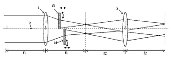
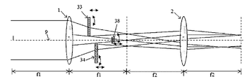
- Embodiment 1 is a real-time variable-parameter optical field modulation system based on two-segment wavelet surface discrete modulation according to Embodiment 1 of the present invention
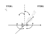
- FIG. 2 is a schematic diagram showing the interference of the double focal beam of the 4F system in the first embodiment of the present invention
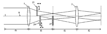
- 3 is a real-time variable-parameter optical field modulation system incorporating a phase-wavelength modulation of a phase-delay device according to a second embodiment of the present invention
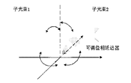
- FIG. 4 is a schematic diagram showing the principle of phase shift of the double-beam interference of the focal plane of the 4F system according to the second embodiment of the present invention.
- FIG. 6 is a schematic diagram of three-beam interference of a back focal plane of a 4F system according to Embodiment 3 of the present invention.
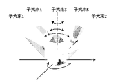
- FIG. 8 is a schematic diagram showing five-beam interference after two-stage modulation of the back focal plane of the 4F system according to Embodiment 4 of the present invention.
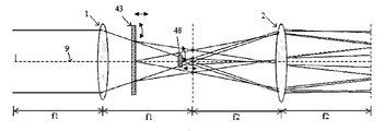
- FIG. 9 is a diagram showing a real-time variable parametric light field modulation system based on modulated sub-wavefront re-segment modulation in a specific embodiment 5 of the present invention.
- FIG. 11 is a schematic diagram showing four-beam interference after two-stage modulation of the back focal plane of the 4F system according to Embodiment 6 of the present invention.
- FIG. 12 is a schematic diagram showing interference of seven beams after two-stage modulation of the back focal plane of the 4F system according to Embodiment 6 of the present invention.
- Embodiment 1 Real-time variable parameter optical field modulation system based on two-segment wavelet surface discrete modulation
- the real-time variable-parameter micro-nano light field modulation system in this embodiment is shown in FIG. 1.
- the sub-element 13 and the sub-element 14 constitute a light-wave-modulating optical component group, at least one of the sub-element 13 and the sub-element 14.
- the sub-element 13 and the sub-element 14 may be a periodic structure or a non-periodic structure;
- the sub-element 13 and the sub-element 14 may be identical. It can also be different.
- the sub-element 13 is a binary optical element that eliminates 0-order light
- the sub-element 14 is a holographic element that eliminates 0-order light
- the sub-element 13 and the sub-element 14 have positive and negative first-order diffracted light
- the first lens After the converging light passes through the sub-element 13 and the sub-element 14 after (group) 1, the positive and negative first-order diffracted lights respectively form two symmetrical converging spots on the back focal plane of the first lens (group) of the 4F optical path system, that is, in the first A lens (group) back focal plane forms four converging spots.
- the dashed line indicates the optical axis 9 of the 4F optical path system.
- the two beams in Fig. 2 correspond to the positive first-order transmitted light field of element 13 and the negative first-order transmitted light field of element 14 under normal incidence of parallel light, respectively. Therefore, different sub-elements are selected to form different interference patterns on the back focal plane of the second lens (set).
- the translating element 13 or the element 14 is changed in the angle between the corresponding output beam and the optical axis in FIG. 2, thereby changing the period of the output pattern; if the center of the element itself is rotated, it is in the figure.
- the corresponding output beam in 2 is rotated about the optical axis to change the orientation of the output pattern.
- Embodiment 2 Real-time variable parameter optical field modulation of segmented wavelet surface modulation added by phase delay device System
- the real-time variable-parameter micro-nano light field modulation system in this embodiment is shown in FIG. 3.
- the sub-element 23 and the sub-element 24 constitute a light-wave-modulating optical component group
- the sub-element 27 is an adjustable phase-phase delay device.
- the sub-element 23 and the sub-element 24 are binary optical elements having only positive and negative first-order diffracted light, two optical interferences are formed on the back focal plane of the second lens (group), as shown in FIG. 4, and corresponding to The beam of sub-element 24 produces a different phase delay under the action of sub-element 27.
- the transmission diffracted light of the sub-elements 23, 24 in the case of normal incidence of parallel light is parallel light, then the two beams in FIG. 4 are parallel light, and the interference pattern is a one-dimensional stripe; Under the adjustment of the element 27, the phase difference between the two beams changes, and the resulting one-dimensional stripe is phase-shifted.
- Embodiment 3 Real-time variable parameter optical field modulation system based on three-segment wavelet surface discrete modulation
- the real-time variable-parameter micro-nano light field modulation system in this embodiment is shown in FIG. 5.
- the sub-elements 33, 34, and 38 constitute a light-wave modulating optical component group, and the first lens in the 4F optical path ( The rear concentrated light wave is separately modulated into three sub-waves, and at least one of the sub-elements 33, 34 and 38 is a binary optical element, a grating element, a hologram element or a super-surface element; the sub-elements 33, 34 and 38 It may be a periodic structure or a non-periodic structure; the sub-elements 33, 34 and 38 may be identical or different.
- the sub-element 33 is a grating element
- the sub-element 34 is a holographic element
- the sub-element 38 is a super-surface element, wherein the rear surface of the sub-elements 33, 34 is in close contact with the mask, and the sub-element 38 only exists.
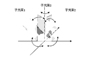
- Class 0 diffracted light is formed on the focal plane of the second lens (group), as shown in FIG. 6, wherein the beam 3 corresponds to the modulation spectrum after the surface element of the meta-op, no matter how the sub-element 38 translates, the beam 3 is always with the light.
- the axes are parallel; if the sub-element 38 rotates about its center, the beam 3 rotates about the optical axis.
- the translation of the sub-elements 33, 34 will change the angle between the beam 1 and the beam 2 and the optical axis; the sub-elements 33, 34 rotate about their own center, and their corresponding beams 1 and 2 will respectively rotate by a corresponding angle around the optical axis;
- the corresponding beam 1 and beam 2 will simultaneously rotate about the optical axis.
- the positive first-order transmission diffracted in the case of normal incidence of parallel light is parallel light; if the sub-element 34 is in the negative first-order transmission diffracted light in the case of normal incidence of parallel light, the leaf-shaped light intensity distribution is obtained; If the zero-order transmitted light of the sub-element 38 in the case of the normal incidence of the parallel light is a spiral light field distribution, then in FIG. 6, the parallel light of the uniform light field, the parallel light of the light field in the shape of a leaf, and the spiral of the light field are respectively formed. The mutual interference between the distributed parallel lights.
- Embodiment 4 Real-time variable parameter optical field modulation system based on modulated wavelet surface remodulation
- the real-time variable-parameter micro-nano light field modulation system in this embodiment is shown in FIG. 7.
- the sub-element 43 and the sub-element 48 constitute a light wave modulation two-group optical component group, and the sub-element 43 is opposite to the first lens. After (group), the beam modulation is concentrated, and the sub-element 48 modulates the wavelet surface modulation of the wavefront with respect to the sub-element 43.
- At least one of the sub-element 43 and the sub-element 48 is one of a binary optical element, a grating element, a hologram element, or a meta-surface element.
- the first lens (group) is then condensed by the sub-element 43 and then diffracted. 0th order, and positive and negative first-order diffracted light, wherein the positive and negative first-order diffracted lights converge on the back focal plane of the first lens (group), and the 0-order light passes through the sub-element 48 to form three beams of concentrated light, and the five sets of light pass through
- the two lenses (groups) form five beams of light as shown in FIG.
- the light beam 3 corresponds to the 0th order diffracted light of the sub-element 48 in the case of normal incidence of parallel light
- the light beams 1, 2 correspond to the sub-element 43 in parallel
- the light beams 4, 5 correspond to the positive and negative first-order diffracted lights of the sub-element 48 in the case of normal incidence of parallel light.
- the sub-element 48 is transposed, the beam 3 is always parallel to the optical axis of the 4F optical path system, and the angle between the beams 4, 5 and the optical axis changes synchronously; the translation sub-element 43, the beam 1, 2 and the optical axis are clamped.
- the angle sync changes. Rotating the sub-element 48, the beams 3, 4, 5 are rotated by respective angles about the optical axis; when the sub-element 43 is rotated, the beams 1, 2 are simultaneously rotated about the optical axis.
- the sub-element 43 and the sub-element 48 constitute two sets of optical modulation device groups.
- Sub-element 43 is modulated for incident light waves
- sub-element 48 is modulated for wavelets of modulated light waves.
- Embodiment 5 Real-time variable parameter optical field modulation system based on sub-wavelength modulation of modulated wavelet surface
- the real-time variable-parameter micro-nano light field modulation system in this embodiment is shown in FIG. 9.
- the sub-element 53 and the sub-elements 55 and 56 constitute a light wave modulation two-component optical component group, and the sub-element 53 pairs
- the first lens (group) is post-convergence beam modulated, its advanced transmitted light is blocked by spatial filtering sub-element 57, and sub-elements 55 and 56 are modulated for sub-wavefront modulation of the post-wavefront for sub-element 53.
- At least one of the sub-elements 53, 55 and the sub-element 56 is one of a binary optical element, a grating element, a hologram element, or a meta-surface element.
- the sub-element 53 is a hologram element
- the sub-element 55 and 56 are anechoic binary optical elements
- the first lens (group) rear condensed light wave converges through the sub-element 53
- a lens (set) back focus is then divergently incident on sub-element 55 and sub-element 56, and the inverse extension of the diffracted light of sub-element 55 and sub-element 56 converges on the back focal plane of the first lens (set).
- the aperture of the second lens (set) is not sufficiently large, only the negative first-order diffracted light of the sub-element 55 and the positive first-order diffracted light of the sub-element 56 pass through the second lens group.
- the back focal plane of the 4F optical path system forms two beams of interference light as shown in FIG. 2.
- the light beam and the light beam 2 correspond to the 0th-order diffracted light of the sub-element 53 in the case where the parallel light is normally incident.
- the sub-element 53 Rotating the sub-element 53, the light beams 1, 2 are rotated around the optical axis of the 4F system; the sub-elements 55, 56 are respectively rotated about their own centers, and the light beams 1, 2 are respectively rotated by respective angles around the optical axis; the sub-elements 55, 56 are simultaneously wound around the optical axis.
- the beams 1, 2 When rotated, the beams 1, 2 are simultaneously rotated by a corresponding angle about the optical axis.
- Embodiment 6 Real-time variable parameter optical field modulation system based on sub-wave surface re-segment modulation after segment modulation
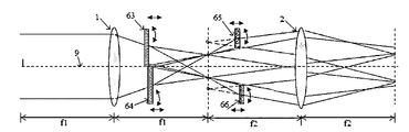
- the real-time variable-parameter micro-nano light field modulation system in this embodiment is shown in FIG. 10.
- the sub-element 63 and the sub-element 64, and the sub-elements 65 and 66 respectively form two sets of optical components, sub-elements.
- 63 and 64 pairs of first lens (group) after convergence beam modulation, sub Elements 65 and 66 are modulated on the wavelet surface after wavelet modulation for the previous optical component group.
- At least one of the sub-elements 63, 64, 65 and 66 is one of a binary optical element, a grating element, a hologram element or a meta-surface element.
- the condensed light passes through the sub-elements 63, 64 to form four converging spots on the back focal plane of the first lens (group), and the sub-element 63 is positive.
- the first-order diffracted light and the negative first-order diffracted light of the sub-element 64 are directly incident on the second lens (group); the negative first-order diffracted light of the sub-element 63 is modulated by the sub-element 66 and then incident on the second lens (group);
- the positive first-order diffracted light of 64 is modulated by the sub-element 65 and then incident on the second lens (group).
- the four beams are parallel beams in which the light fields are uniformly distributed.
- the elements 63, 64, 65, 66 rotate about the optical axis, and the four beams simultaneously rotate about the optical axis.
- the four beams of light may interfere in the same interference plane, or they may interfere in two mutually perpendicular planes, and the interference light field is geometrically superimposed.
- the sub-element 68 has a 0-order and a high-order transmission, and at least 7 sub-wave faces exist after the sub-element 68.
- the partial wavefront modulated by the sub-elements 63 and 64 is modulated by the sub-elements 65 and 66, and the sub-wavefront below the optical axis is modulated by the sub-element 67, and finally at least seven interfering beams are formed on the focal plane of the 4F optical path system.
- the sub-element 67 is a phase delay device, the interference pattern produces a phase shift at a different phase delay of the sub-element 67.
- the incident light of the 4F optical path system is parallel to the optical axis.
- the incident light has an angle with the optical axis, the light wave propagation direction after passing through the previous optical modulation device still converges on the first lens (group).
- the back focal plane only shifts the spot position along the incident light direction.
- the embodiment of the real-time variable-parameter micro-nano light field modulation system is not limited to the above embodiment; the modulation sub-component constituting the optical device group is not limited to the above optical element; the sub-element may be one-dimensional or multi-dimensional periodicity Or a non-periodic structure; the incidence of the 4F system Light is parallel light, but not limited to parallel light.
- the system of the present invention uses a laser as a light source to generate a real-time, continuously adjustable interference pattern of periodic, orientation, duty cycle and other structural parameters through a 4F optical path system and a discrete optical modulation device, integrated in various lithography.
- the system prepares micro-nano patterns with different structural parameters in real-time on the surface of positive and negative photoresists, providing a basis for new functional materials based on micro-nanostructures.
Landscapes
- Physics & Mathematics (AREA)
- General Physics & Mathematics (AREA)
- Optics & Photonics (AREA)
- Holo Graphy (AREA)
- Mechanical Light Control Or Optical Switches (AREA)
Abstract
一种实时变参量微纳米光场调制系统和干涉光刻系统,该光场调制系统包括光源、4F光学系统和光波调制光学元器件组,4F光学系统包括沿光路依次设置的第一光学组件(1)和第二光学组件(2),光波调制光学元器件组设置于第一光学组件(1)和第二光学组件(2)之间,该光波调制光学元器件组通过对子波面分段调制,在系统的后焦面产生图案及结构参数可调的光场分布。通过子元件(13, 14, 23, 24, 27, 33, 34, 38,43, 48, 53, 55, 56, 63, 64, 65, 66, 67, 68)实现对子波面的分立、实时调控,通过改变子元件(13, 14, 23, 24, 27, 33, 34, 38,43, 48, 53, 55, 56, 63, 64, 65, 66, 67, 68)组合方式可实现不同微纳米图案的实时输出,通过子元件(13, 14, 23, 24, 27, 33, 34, 38,43, 48, 53, 55, 56, 63, 64, 65, 66, 67, 68)的位置或子元件(13, 14, 23, 24, 27, 33, 34, 38,43, 48, 53, 55, 56, 63, 64, 65, 66, 67, 68)间相对位置变化可实现结构参数的连续调制。该系统可灵活集成于各种光刻或显微系统中,实现变参量微纳米结构的实时写入和可调制微纳米结构光检测。
Description
本发明涉及一种实时变参量微纳米光场调制系统和干涉光刻系统,具体涉及一种多子波面实时、分立、连续调制的变参量光场调制系统,应用于微纳米结构加工、激光共焦显微成像、生物荧光检测和微纳米形貌检测。
干涉光刻或全息光刻是一种高效制备大幅面微纳米结构的技术,干涉光刻制备的微纳米结构,其周期由干涉光束的波长与夹角共同确定(周期大小与干涉波长成正比,与干涉光束夹角的正弦值成反比);其取向由干涉光束的波矢决定;其条纹位相分布由干涉光束的相对位相差决定。干涉光刻可与其他技术如蒸镀、刻蚀等自由组合,为微纳米结构在光子晶体、生物医学、微电子等领域的应用提供基础。
干涉光刻系统分为分振幅(Amplitude-splitting configurations)干涉系统和分波面(Wavefront-splitting configurations)干涉系统,两种系统均通过分光器件将入射光分为两束或两束以上相干光进行干涉,通常选用半透半反镜、棱镜、光栅、衍射掩膜以及Lloyd’s镜等作为分光器件。无论采用何种分光器件实现多光束干涉,其制备的微纳米结构的结构参数为固定值,不可实时变化。即使采用万向镜(gimbal mirror),也只能在有限的范围内改变微纳米结构的周期,而基于gimbal mirror实现周期和取向两种参数实时变化的干涉系统,其光学设置十分复杂。
为实现微纳米结构空频调制,专利U.S.patent 5,132,812及其改进专利U.S.patent 5,262,879、U.S.patent 5,822,092以及U.S.patent 5,132,812通过三组不同夹角的光束干涉形成了三种不同空频的光栅像素,实现了
光栅空频的离散调制。中国专利CN01134127.0、200510095775.2、200510095776.7、CN201010238377.2以及CN201010503788.X公开了一种以二元光栅作为分光元件,通过切换不同空频的分光光栅来实现空频的离散调制。
而目前基于微纳米结构的新材料,如新型颜色显示、真彩色3D显示以及超颖表面材料(metasurface),对光刻系统提出了周期、取向、占空比甚至图案等参数实时制备的需求。
【发明内容】
本发明的目的在于提供一种实时变参量微纳米光场调制系统和干涉光刻系统,可灵活集成于各种光刻系统中,实现微纳米结构的实时制备,亦可集成于各种显微系统中,提供可调制结构光照明。
为实现上述目的,本发明提供如下技术方案:
本申请实施例公开了一种实时变参量微纳米光场调制系统,包括光源、4F光学系统和光波调制光学元器件组,所述4F光学系统包括沿光路依次设置的第一光学组件和第二光学组件,所述光波调制光学元器件组设置于所述第一光学组件和第二光学组件之间,该光波调制光学元器件组通过对子波面分段调制,在系统的后焦面产生图案及其结构参数可调的光场分布。
在该技术方案中,第一光学组件和第二光学组件可以为单独一个透镜,也可以为多个透镜构成的组合。
优选的,在上述的实时变参量微纳米光场调制系统中,所述结构参数包括周期、取向、相位或相移量和占空比。
优选的,在上述的实时变参量微纳米光场调制系统中,所述光场分布为干涉图案。
优选的,在上述的实时变参量微纳米光场调制系统中,所述结构参
数实时、分立或同步、连续可调。
优选的,在上述的实时变参量微纳米光场调制系统中,所述第一光学组件和第二光学组件为透镜、透镜组或具有相同光学性能的超颖表面器件、微纳米结构。
优选的,在上述的实时变参量微纳米光场调制系统中,所述光波调制光学元器件组包括多个子元件,通过选用不同的子元件或/和不同的组合方式实现对各子波面的不同光场调制,并在系统的后焦面产生实现不同图案的光场分布;所述子元件通过位移变化、和/或旋转实现对各子波面的光场调制,并在系统的后焦面产生结构参数可调的光场分布。
在该技术方案中,子元件可针对不同子波面实时、独立调制,子元件运动方式,由计算机和精密控制系统共同完成。
在该技术方案中,子元件可以为任意周期结构或非周期结构。
优选的,在上述的实时变参量微纳米光场调制系统中,所述子元件选自位相元件、二元光学元件、光栅元件、全息元件、反射元件、折射元件和超颖表面元件。
优选的,在上述的实时变参量微纳米光场调制系统中,所述光波调制光学元器件组沿光路方向包括多级子器件组,每级子器件组包括至少一个所述子元件,其中位于后一级的子器件组用以对前一级调制后波面的子波面实时调制。
在该技术方案中,该处的调制是指通过子元件的移动和/或旋转实现对子波面光束路线的改变。
优选的,在上述的实时变参量微纳米光场调制系统中,所述光学元器件组还可包含可调节光阑、灰度掩膜、偏振转换元件中的一种或多种组合。
优选的,在上述的实时变参量微纳米光场调制系统中,所述光源包括激光。进一步地,光源由激光器或其他相干光源提供。其产生的入射
光为平行光。
本申请实施例还公开了一种微纳米结构的干涉光刻系统,包括所述的实时变参量微纳米光场调制系统。
在该技术方案中,调制后的不同子波面在4F系统的后焦面形成多路光束,不同的光束在重叠区域可相互干涉,可相互叠加,可同时干涉和叠加。
实时变参量微纳米光场调制系统还可灵活集成于各种显微系统中。
与现有技术相比,本发明的优点在于:
(1)、通过不同分立子元件的组合,实现不同图案的制备。与空间滤波设备和精密控制平台相结合,实现像素化图案制备。
(2)、通过分别调制子元件,实现多维图案在不同维度下结构参数的独立可调。
(3)、通过子元件的平移和旋转,实现图案在单维度下结构参数的连续调制。
总之,本发明利用不同的子元件组成光学调制器件组,对入射光子波面实现实时分段调制,对调制后子波面分段调制等联合调制方法,实现各种复杂微纳米结构的实时制备,并实现其结构参数的实时、连续可调。
为了更清楚地说明本申请实施例或现有技术中的技术方案,下面将对实施例或现有技术描述中所需要使用的附图作简单地介绍,显而易见地,下面描述中的附图仅仅是本申请中记载的一些实施例,对于本领域普通技术人员来讲,在不付出创造性劳动的前提下,还可以根据这些附图获得其他的附图。
图1所示为本发明具体实施例1中基于两段子波面分立调制的实时变参量光场调制系统;
图2所示为本发明具体实施例1中4F系统后焦面双光束干涉示意图;
图3所示为本发明具体实施例2中加入位相延迟器件分段子波面调制的实时变参量光场调制系统;
图4所示为本发明具体实施例2中4F系统后焦面双光束干涉相移原理示意图;
图5所示为本发明具体实施例3中基于三段子波面分立调制的实时变参量光场调制系统;
图6所示为本发明具体实施例3中4F系统后焦面三光束干涉示意图;
图7所示为本发明具体实施例4中基于调制后子波面再调制的实时变参量光场调制系统;
图8所示为本发明具体实施例4中4F系统后焦面两级调制后五光束干涉示意图;
图9所示为本发明具体实施例5中基于调制后子波面再分段调制的实时变参量光场调制系统;
图10所示为本发明具体实施例6中基于分段调制后子波面再分段调制的实时变参量光场调制系统;
图11所示为本发明具体实施例6中4F系统后焦面两级调制后四光束干涉示意图;
图12所示为本发明具体实施例6中4F系统后焦面两级调制后七光束干涉示意图,
下面将结合本发明实施例中的附图,对本发明实施例中的技术方案进行详细的描述,显然,所描述的实施例仅仅是本发明一部分实施例,
而不是全部的实施例。基于本发明中的实施例,本领域普通技术人员在没有做出创造性劳动的前提下所获得的所有其他实施例,都属于本发明保护的范围。
实施例一:基于两段子波面分立调制的实时变参量光场调制系统
本实施例中所述实时变参量微纳米光场调制系统如图1所示,在4F光路系统中,子元件13和子元件14组成光波调制光学元器件组,子元件13和子元件14中至少一个是二元光学元件、光栅元件、全息元件或超颖表面元件的一种;子元件13和子元件14可以是周期性结构,亦可以为非周期性结构;子元件13和子元件14可以完全相同,也可以不同。
在本实施例中,若子元件13为消0级光的二元光学元件,子元件14为消0级光的全息元件,子元件13和子元件14具有正负一级衍射光,则第一透镜(组)1后的会聚光经子元件13和子元件14后,其正负一级衍射光分别在4F光路系统的第一透镜(组)后焦面形成两个对称的会聚光斑,即在第一透镜(组)后焦面形成四个会聚光斑。在没有其他辅助光学元件时,若第二透镜(组)2的口径不是足够大,则仅子元件13的正一级衍射光以及子元件14的负一级衍射光进入第二透镜(组),并在第二透镜(组)的后焦面形成两束光相干涉,
如图2所示,其中虚线表示4F光路系统的光轴9。图2中的两束光分别对应于平行光垂直入射条件下,元件13的正一级透射光场和元件14的负一级透射光场。因此,选用不同的子元件在第二透镜(组)的后焦面会形成不同的干涉图案。
在本实施例中,若平移元件13或元件14,其在图2中对应的输出光束与光轴的夹角发生改变,从而改变输出图案的周期;若绕元件本身的中心旋转,其在图2中对应的输出光束则绕光轴旋转,从而改变输出图案的取向。
实施例二:加入位相延迟器件分段子波面调制的实时变参量光场调
制系统
本实施例中所述实时变参量微纳米光场调制系统如图3所示,在4F光路系统中,子元件23和子元件24组成光波调制光学元器件组,子元件27为可调节位相延迟器件。若子元件23和子元件24均为只存在正负一级衍射光的二元光学元件,则在第二透镜(组)的后焦面形成两束光相干涉,如图4所示,并且对应于子元件24的光束在子元件27的作用下产生不同的位相延迟。在本实施例中,子元件23、24在平行光垂直入射情况下的透射衍射光均为平行光,则图4中两束光均为平行光,干涉图案为一维条纹;随着在子元件27的调节下,两束光的位相差发生改变,则产生的一维条纹随之发生相移。
实施例三:基于三段子波面分立调制的实时变参量光场调制系统
本实施例中所述实时变参量微纳米光场调制系统如图5所示,在4F光路系统中,子元件33、34和38组成光波调制光学元器件组,将4F光路中第一透镜(组)后面的会聚光波分成三段子波分别调制,子元件33、34和38中至少一个是二元光学元件、光栅元件、全息元件或超颖表面元件的一种;子元件33、34和38可以是周期性结构,亦可以为非周期性结构;子元件33、34和38可以完全相同,也可以不同。
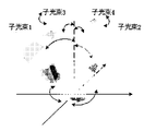
在本实施例中,若子元件33为光栅元件,子元件34为全息元件,子元件38为超颖表面元件,其中子元件33、34后表面紧贴掩膜消0极光,子元件38只存在0级衍射光。则在即在第二透镜(组)后焦面形成三束光,如图6所示,其中光束3对应于经超颖表面元件后的调制光谱,无论子元件38如何平移,光束3始终与光轴平行;若子元件38绕自身中心旋转,则光束3绕光轴旋转。子元件33、34的平移将分布改变光束1和光束2与光轴的夹角;子元件33、34绕自身中心旋转,其对应光束1和光束2将分别绕光轴旋转相应的角度;子元件33、34同时绕光轴旋转,则对应光束1和光束2将同时绕光轴旋转。
若子元件33为一维光栅,其在平行光垂直入射情况下的正一级透射衍射为平行光;若子元件34在平行光垂直入射情况下的负一级透射衍射光呈树叶形光强分布;若子元件38在平行光垂直入射情况下的0级透射光为螺旋形光场分布;则图6中分别为光场均一的平行光、光场呈树叶形分布的平行光以及光场成螺旋形分布的平行光之间的相互干涉。
实施例四:基于调制后子波面再调制的实时变参量光场调制系统
本实施例中所述实时变参量微纳米光场调制系统如图7所示,在4F光路系统中,子元件43和子元件48组成光波调制两组光学元器件组,子元件43对第一透镜(组)后会聚光束调制,子元件48针对子元件43调制后波面的子波面调制。子元件43和子元件48中至少一个是二元光学元件、光栅元件、全息元件或超颖表面元件的一种。
在本实施例中,若子元件43为具有多级透射的一维光栅,子元件48为具有多级透射的超颖表面器件,则第一透镜(组)后会聚波经子元件43后,衍射出0级、以及正负一级衍射光,其中正负一级衍射光会聚于第一透镜(组)后焦面,0级光经子元件48后形成三束会聚光,五组光线经第二透镜(组)形成如图8所示的五束光相互干涉,其中光束3对应于子元件48在平行光垂直入射情况下的0级衍射光,光束1、2对应于子元件43在平行光垂直入射情况下的正负一级衍射光,光束4、5对应于子元件48在平行光垂直入射情况下的正负一级衍射光。在本实施例中,平移子元件48,光束3始终与4F光路系统的光轴平行,光束4、5与光轴的夹角同步改变;平移子元件43,光束1、2与光轴的夹角同步改变。旋转子元件48,则光束3、4、5绕光轴旋转相应角度;旋转子元件43,则光束1、2同时绕光轴旋转。
因此,在本实施例中,子元件43和子元件48组成两组光学调制器件组。子元件43针对入射光波调制,子元件48针对调制后光波的子波调制。
实施例五:基于调制后子波面再分段调制的实时变参量光场调制系统
本实施例中所述实时变参量微纳米光场调制系统如图9所示,在4F光路系统中,子元件53、子元件55和56组成光波调制两组光学元器件组,子元件53对第一透镜(组)后会聚光束调制,其高级透射光被空间滤波子元件57阻拦,子元件55和56针对子元件53调制后波面的子波面调制。子元件53、55和子元件56中至少一个是二元光学元件、光栅元件、全息元件或超颖表面元件的一种。
若子元件53为全息元件,子元件55和56为消0极光二元光学元件,若子元件53的高级衍射光被子元件57阻挡,则第一透镜(组)后会聚光波经子元件53会聚于第一透镜(组)后焦点,再发散入射至子元件55和子元件56,子元件55和子元件56衍射光的反向延长线会聚于第一透镜(组)后焦面。在没有其他辅助光学元件时,在第二透镜(组)的口径不足够大的情况下,仅子元件55的负一级衍射光和子元件56的正一级衍射光会经过第二透镜组到达4F光路系统的后焦面,形成如图2所示的两束干涉光。在本实施例中光束、光束2分别对应于子元件53在平行光垂直入射情况下的0级衍射光。旋转子元件53,光束1、2绕4F系统的光轴旋转;子元件55、56分别绕自身中心旋转,则光束1、2分别绕光轴旋转相应角度;子元件55、56同时绕光轴旋转,则光束1、2同时绕光轴旋转相应角度。
实施例六:基于分段调制后子波面再分段调制的实时变参量光场调制系统
本实施例中所述实时变参量微纳米光场调制系统如图10所示,在4F光路系统中,子元件63和子元件64、子元件65和66分别组成两组光学元器件组,子元件63和64对第一透镜(组)后会聚光束调制,子
元件65和66针对前一光学元件组调制后子波面子波面调制。子元件63、64、65和66中至少一个是二元光学元件、光栅元件、全息元件或超颖表面元件的一种。
若子元件63、64、65和66均为消0级光二元位相元件,则会聚光经子元件63、64后在第一透镜(组)后焦面形成4个会聚光斑,子元件63的正一级衍射光和子元件64的负一级衍射光直接入射至第二透镜(组);子元件63的负一级衍射光,经子元件66调制后入射至第二透镜(组);子元件64的正一级衍射光经子元件65调制后入射至第二透镜(组)。在4F光路系统后焦面,形成如图11所示的四路干涉光束,在本实施例中,四路光束均为光场均匀分布的平行光束。分别平移子元件63、64、65、66,其对应光束与光轴的夹角发生改变;分别绕子元件63、64、65、66自身中心旋转,其对应光束绕光轴旋转;同时将子元件63、64、65、66绕光轴转动,四束光同时绕光轴转动。
如图11中所示四束光可以在同一干涉平面内干涉,也可以在两个互相垂直的平面内两两干涉,干涉光光场几何叠加。
若子元件63和64未消0级光,且其0级光经子元件68调制,如图12所示,子元件68具有0级及高级次透射,则在子元件68后至少存在7个子波面,其中经子元件63和64调制后的部分波面再经子元件65和66调制,光轴下方子波面再经经子元件67调制,最终在在4F光路系统后焦面形成至少七路干涉光束,若子元件67为位相延迟器件,则在子元件67不同的位相延迟下,干涉图案产生相移。
以上实施例中,4F光路系统的入射光与光轴平行,当入射光与光轴有夹角时,其经前一组光学调制器件后的光波传播方向仍然会聚于第一透镜(组)的后焦面,仅会聚光斑位置沿入射光方向平移。
所述实时变参量微纳米光场调制系统的实施方式并不仅限于上述实施例;所述组成光学器件组的调制子元件并不仅限于上述光学元件;所述子元件可以为一维或多维周期性或非周期性结构;所述4F系统的入射
光为平行光,但不仅限于平行光。
综上所述,本发明系统用激光作为光源,通过4F光路系统和分立的光学调制器件,产生周期、取向、占空比等结构参数实时、连续可调的干涉图案,集成于各种光刻系统,在正负光刻胶表面实时制备不同结构参数的微纳米图案,为基于微纳米结构的新型功能材料提供基础。
需要说明的是,在本文中,诸如第一和第二等之类的关系术语仅仅用来将一个实体或者操作与另一个实体或操作区分开来,而不一定要求或者暗示这些实体或操作之间存在任何这种实际的关系或者顺序。而且,术语“包括”、“包含”或者其任何其他变体意在涵盖非排他性的包含,从而使得包括一系列要素的过程、方法、物品或者设备不仅包括那些要素,而且还包括没有明确列出的其他要素,或者是还包括为这种过程、方法、物品或者设备所固有的要素。在没有更多限制的情况下,由语句“包括一个……”限定的要素,并不排除在包括所述要素的过程、方法、物品或者设备中还存在另外的相同要素。
以上所述仅是本申请的具体实施方式,应当指出,对于本技术领域的普通技术人员来说,在不脱离本申请原理的前提下,还可以做出若干改进和润饰,这些改进和润饰也应视为本申请的保护范围。
Claims (11)
- 一种实时变参量微纳米光场调制系统,其特征在于,包括光源、4F光学系统和光波调制光学元器件组,所述4F光学系统包括沿光路依次设置的第一光学组件和第二光学组件,所述光波调制光学元器件组设置于所述第一光学组件和第二光学组件之间,该光波调制光学元器件组通过对子波面分段调制,在系统的后焦面产生图案及其结构参数可调的光场分布。
- 根据权利要求1所述的实时变参量微纳米光场调制系统,其特征在于:所述结构参数包括周期、取向、相位或相移量和占空比。
- 根据权利要求1所述的实时变参量微纳米光场调制系统,其特征在于:所述光场分布为干涉图案。
- 根据权利要求1所述的实时变参量微纳米光场调制系统,其特征在于:所述结构参数实时、分立或同步、连续可调。
- 根据权利要求1所述的实时变参量微纳米光场调制系统,其特征在于:所述第一光学组件和第二光学组件为透镜、透镜组或具有相同光学性能的超颖表面器件、微纳米结构。
- 根据权利要求1至5任一所述的实时变参量微纳米光场调制系统,其特征在于:所述光波调制光学元器件组包括多个子元件,通过选用不同的子元件或/和不同的组合方式实现对各子波面的光场调制,并在系统的后焦面产生实现不同图案的光场分布;所述子元件通过位移变化、和/或旋转实现对各子波面的光场调制,并在系统的后焦面产生结构参数可调的光场分布。
- 根据权利要求6所述的实时变参量微纳米光场调制系统,其特征在于:所述子元件选自位相元件、二元光学元件、光栅元件、全息元件、反射元件、折射元件和超颖表面元件。
- 根据权利要求6所述的实时变参量微纳米光场调制系统,其特征 在于:所述光波调制光学元器件组沿光路方向包括多级子器件组,每级子器件组包括至少一个所述子元件,其中位于后一级的子器件组用以对前一级调制后波面的子波面实时调制。
- 根据权利要求6所述的实时变参量微纳米光场调制系统,其特征在于:所述光学元器件组还可包含可调节光阑、灰度掩膜、偏振转换元件中的一种或多种组合。
- 根据权利要求1所述的实时变参量微纳米光场调制系统,其特征在于:所述光源包括激光。
- 一种微纳米结构的干涉光刻系统,其特征在于,包括权利要求1至10任一所述的实时变参量微纳米光场调制系统。
Priority Applications (2)
| Application Number | Priority Date | Filing Date | Title |
|---|---|---|---|
| US15/310,245 US10054859B2 (en) | 2016-01-06 | 2016-01-06 | Real-time variable parameter micro-nano optical field modulation system and interference lithography system |
| PCT/CN2016/070306 WO2017117751A1 (zh) | 2016-01-06 | 2016-01-06 | 实时变参量微纳米光场调制系统和干涉光刻系统 |
Applications Claiming Priority (1)
| Application Number | Priority Date | Filing Date | Title |
|---|---|---|---|
| PCT/CN2016/070306 WO2017117751A1 (zh) | 2016-01-06 | 2016-01-06 | 实时变参量微纳米光场调制系统和干涉光刻系统 |
Publications (1)
| Publication Number | Publication Date |
|---|---|
| WO2017117751A1 true WO2017117751A1 (zh) | 2017-07-13 |
Family
ID=59273332
Family Applications (1)
| Application Number | Title | Priority Date | Filing Date |
|---|---|---|---|
| PCT/CN2016/070306 Ceased WO2017117751A1 (zh) | 2016-01-06 | 2016-01-06 | 实时变参量微纳米光场调制系统和干涉光刻系统 |
Country Status (2)
| Country | Link |
|---|---|
| US (1) | US10054859B2 (zh) |
| WO (1) | WO2017117751A1 (zh) |
Cited By (2)
| Publication number | Priority date | Publication date | Assignee | Title |
|---|---|---|---|---|
| CN114839771A (zh) * | 2022-04-24 | 2022-08-02 | 北京理工大学 | 一种基于超颖表面的微型大视场局部放大光学系统 |
| CN115164714A (zh) * | 2022-08-18 | 2022-10-11 | 深圳迈塔兰斯科技有限公司 | 一种干涉系统 |
Families Citing this family (11)
| Publication number | Priority date | Publication date | Assignee | Title |
|---|---|---|---|---|
| GB2578236B (en) | 2017-05-24 | 2022-11-09 | Univ Columbia | Broadband achromatic flat optical components by dispersion-engineered dielectric metasurfaces |
| EP3676973A4 (en) | 2017-08-31 | 2021-05-05 | Metalenz, Inc. | INTEGRATION OF LENS WITH PERMEABLE METAL SURFACE |
| US11183769B2 (en) | 2017-10-27 | 2021-11-23 | Thales Canada Inc. | Near-grazing retroreflectors for polarization |
| EP4729996A2 (en) | 2018-01-24 | 2026-04-22 | President And Fellows Of Harvard College | Polarization state generation with a metasurface |
| KR102869686B1 (ko) | 2018-07-02 | 2025-10-14 | 메탈렌츠 인코포레이티드 | 레이저 스펙클 감소를 위한 메타표면들 |
| CN114286953B (zh) | 2019-07-26 | 2025-04-01 | 梅特兰兹股份有限公司 | 孔隙-超表面和混合折射-超表面成像系统 |
| US11578968B1 (en) | 2019-10-31 | 2023-02-14 | President And Fellows Of Harvard College | Compact metalens depth sensors |
| CN110703577B (zh) * | 2019-11-21 | 2022-03-04 | 苏州大学 | 超表面彩色全息的制备方法及光学系统 |
| CN112099121B (zh) * | 2020-09-29 | 2022-07-22 | 北京华卓精科科技股份有限公司 | 基于4f系统的扫描干涉光刻系统 |
| EP4348780A4 (en) | 2021-05-25 | 2025-04-23 | Metalenz, Inc. | Single element dot pattern projector |
| WO2024205646A2 (en) | 2022-03-31 | 2024-10-03 | Metalenz, Inc. | Polarization sorting metasurface microlens array device |
Citations (6)
| Publication number | Priority date | Publication date | Assignee | Title |
|---|---|---|---|---|
| CN1786748A (zh) * | 2005-11-17 | 2006-06-14 | 苏州大学 | 衍射光变图像的高速激光直写方法和系统 |
| CN102073264A (zh) * | 2010-11-19 | 2011-05-25 | 中山大学 | 分时复用计算全息三维显示系统及其显示方法 |
| CN102576152A (zh) * | 2009-07-31 | 2012-07-11 | 卡尔蔡司激光器材有限责任公司 | 产生处理基底的光束的光学系统 |
| WO2013102464A1 (en) * | 2012-01-06 | 2013-07-11 | Danmarks Tekniske Universitet | 4f-based optical phase imaging system |
| CN103246195A (zh) * | 2013-05-08 | 2013-08-14 | 苏州苏大维格光电科技股份有限公司 | 三维激光打印方法与系统 |
| CN103488036A (zh) * | 2013-09-24 | 2014-01-01 | 苏州苏大维格光电科技股份有限公司 | 全息立体投影屏及其投影方法 |
Family Cites Families (9)
| Publication number | Priority date | Publication date | Assignee | Title |
|---|---|---|---|---|
| US5262879A (en) | 1988-07-18 | 1993-11-16 | Dimensional Arts. Inc. | Holographic image conversion method for making a controlled holographic grating |
| US5822092A (en) | 1988-07-18 | 1998-10-13 | Dimensional Arts | System for making a hologram of an image by manipulating object beam characteristics to reflect image data |
| JP2508387B2 (ja) | 1989-10-16 | 1996-06-19 | 凸版印刷株式会社 | 回折格子パタ―ンを有するディスプレイの作製方法 |
| CA2389937A1 (en) * | 2001-06-11 | 2002-12-11 | Jds Uniphase Inc. | Multi-pass configurations |
| WO2003034118A1 (en) * | 2001-10-17 | 2003-04-24 | Risø National Laboratory | A system for electromagnetic field conversion |
| CN1182445C (zh) | 2001-10-29 | 2004-12-29 | 苏州大学 | 光学可变图像的制作方法及其照排系统 |
| CN100349024C (zh) | 2005-11-17 | 2007-11-14 | 苏州大学 | 微光变图像的激光直写方法及装置 |
| CN101930207B (zh) | 2010-07-28 | 2012-02-15 | 苏州苏大维格光电科技股份有限公司 | 一种微光栅亚像素三维光学图像及其制作方法 |
| CN101976020B (zh) | 2010-10-12 | 2012-08-22 | 苏州苏大维格光电科技股份有限公司 | 一种光刻装置和光刻方法 |
-
2016
- 2016-01-06 WO PCT/CN2016/070306 patent/WO2017117751A1/zh not_active Ceased
- 2016-01-06 US US15/310,245 patent/US10054859B2/en active Active
Patent Citations (6)
| Publication number | Priority date | Publication date | Assignee | Title |
|---|---|---|---|---|
| CN1786748A (zh) * | 2005-11-17 | 2006-06-14 | 苏州大学 | 衍射光变图像的高速激光直写方法和系统 |
| CN102576152A (zh) * | 2009-07-31 | 2012-07-11 | 卡尔蔡司激光器材有限责任公司 | 产生处理基底的光束的光学系统 |
| CN102073264A (zh) * | 2010-11-19 | 2011-05-25 | 中山大学 | 分时复用计算全息三维显示系统及其显示方法 |
| WO2013102464A1 (en) * | 2012-01-06 | 2013-07-11 | Danmarks Tekniske Universitet | 4f-based optical phase imaging system |
| CN103246195A (zh) * | 2013-05-08 | 2013-08-14 | 苏州苏大维格光电科技股份有限公司 | 三维激光打印方法与系统 |
| CN103488036A (zh) * | 2013-09-24 | 2014-01-01 | 苏州苏大维格光电科技股份有限公司 | 全息立体投影屏及其投影方法 |
Cited By (2)
| Publication number | Priority date | Publication date | Assignee | Title |
|---|---|---|---|---|
| CN114839771A (zh) * | 2022-04-24 | 2022-08-02 | 北京理工大学 | 一种基于超颖表面的微型大视场局部放大光学系统 |
| CN115164714A (zh) * | 2022-08-18 | 2022-10-11 | 深圳迈塔兰斯科技有限公司 | 一种干涉系统 |
Also Published As
| Publication number | Publication date |
|---|---|
| US10054859B2 (en) | 2018-08-21 |
| US20180039183A1 (en) | 2018-02-08 |
Similar Documents
| Publication | Publication Date | Title |
|---|---|---|
| US10054859B2 (en) | Real-time variable parameter micro-nano optical field modulation system and interference lithography system | |
| Khonina et al. | Exploring diffractive optical elements and their potential in free space optics and imaging‐A comprehensive review | |
| Xue et al. | Polarized holographic lithography system for high-uniformity microscale patterning with periodic tunability | |
| CN103235489B (zh) | 可变周期多光束干涉光刻的方法 | |
| US20200272100A1 (en) | Systems and methods for controlling electromagnetic radiation | |
| Xue et al. | Development of dielectric-film-based polarization modulation scheme for patterning highly uniform 2d array structures with periodic tunability | |
| KR20210106516A (ko) | 선형 편광 전환 소자, 제조 방법 및 선형 편광 전환 시스템 | |
| CN106950704A (zh) | 可调椭圆矢量空心光束产生装置 | |
| CN110703577B (zh) | 超表面彩色全息的制备方法及光学系统 | |
| CN108983560A (zh) | 一种可控周期和方向的干涉光刻系统 | |
| US7830578B2 (en) | Apparatus for electronically controlled holograms | |
| CN107229126A (zh) | 一种微纳米光场实时构建调制系统和方法 | |
| CN111290147A (zh) | 光束偏振态的调控装置和方法 | |
| CN105511074B (zh) | 实时变参量微纳米光场调制系统和干涉光刻系统 | |
| CN108227063B (zh) | 一种集成偏振光栅制备系统及方法 | |
| CN205942088U (zh) | 实时变参量微纳米光场调制与光刻系统 | |
| JP2023169127A (ja) | マルチビーム3d焦点生成器 | |
| CN101566732B (zh) | 利用计算全息产生柱矢量光束的方法 | |
| CN207301512U (zh) | 一种微纳米光场实时构建调制系统 | |
| CN117991491B (zh) | 基于色散双螺旋点扩散函数超构透镜显微成像方法及装置 | |
| Song et al. | Multi-functional dual-path self-aligned polarization interference lithography | |
| CN109643025B (zh) | 具有用于制造gpoe的应用的旋转几何相位全息图 | |
| CN101833135B (zh) | 透射式光栅相移器 | |
| CN100371771C (zh) | 一种消色差变色银衍射图像的制作方法 | |
| CN114518653A (zh) | 基于复振幅光场调控技术的光束扫描方法与装置 |
Legal Events
| Date | Code | Title | Description |
|---|---|---|---|
| WWE | Wipo information: entry into national phase |
Ref document number: 15310245 Country of ref document: US |
|
| 121 | Ep: the epo has been informed by wipo that ep was designated in this application |
Ref document number: 16882896 Country of ref document: EP Kind code of ref document: A1 |
|
| NENP | Non-entry into the national phase |
Ref country code: DE |
|
| 122 | Ep: pct application non-entry in european phase |
Ref document number: 16882896 Country of ref document: EP Kind code of ref document: A1 |