WO2017090436A1 - アンテナ装置および電子機器 - Google Patents
アンテナ装置および電子機器 Download PDFInfo
- Publication number
- WO2017090436A1 WO2017090436A1 PCT/JP2016/083309 JP2016083309W WO2017090436A1 WO 2017090436 A1 WO2017090436 A1 WO 2017090436A1 JP 2016083309 W JP2016083309 W JP 2016083309W WO 2017090436 A1 WO2017090436 A1 WO 2017090436A1
- Authority
- WO
- WIPO (PCT)
- Prior art keywords
- antenna device
- antenna
- coil
- coil antenna
- notch
- Prior art date
- Legal status (The legal status is an assumption and is not a legal conclusion. Google has not performed a legal analysis and makes no representation as to the accuracy of the status listed.)
- Ceased
Links
Images








Classifications
-
- H—ELECTRICITY
- H01—ELECTRIC ELEMENTS
- H01Q—ANTENNAS, i.e. RADIO AERIALS
- H01Q7/00—Loop antennas with a substantially uniform current distribution around the loop and having a directional radiation pattern in a plane perpendicular to the plane of the loop
- H01Q7/06—Loop antennas with a substantially uniform current distribution around the loop and having a directional radiation pattern in a plane perpendicular to the plane of the loop with core of ferromagnetic material
-
- H—ELECTRICITY
- H01—ELECTRIC ELEMENTS
- H01Q—ANTENNAS, i.e. RADIO AERIALS
- H01Q19/00—Combinations of primary active antenna elements and units with secondary devices, e.g. with quasi-optical devices, for giving the antenna a desired directional characteristic
- H01Q19/02—Details
Definitions
- the present invention relates to an antenna device having a coil antenna, and more particularly to an antenna device used together with a planar conductor and an electronic apparatus including the antenna device.
- Patent Document 1 discloses an antenna device that efficiently emits magnetic flux by coupling a coil antenna to a planar conductor. As described above, when an antenna device using a coil antenna is provided in an electronic device including a planar conductor, the antenna device is easily incorporated into the electronic device by providing the planar conductor so as not to shield the magnetic flux of the coil antenna. Can do.
- the end of the metal casing is often bent in order to increase the rigidity while increasing the internal space.
- the inventors of the present application have found that the shape of the metal casing has a great influence on the characteristics of the antenna when an antenna device including such a metal casing having a bent end and a coil antenna is configured. That is, a strong eddy current flows through the metal casing when the magnetic flux interlinking the coil antenna tries to pass through the bent end of the metal casing. It has been found that this is one cause of characteristic deterioration such as a decrease in Q value and an increase in loss of the antenna device.
- An object of the present invention is to provide an antenna device and an electronic device including the antenna device in which deterioration of characteristics of the antenna device described above is suppressed.
- the antenna device of the present invention is coupled to a coil antenna having a coil conductor wound around a winding axis and at least a part of the coil antenna when viewed in plan in the direction of the winding axis.
- a planar conductor having a main surface, The planar conductor has a bent portion at an end portion of the main surface, and a notch is formed in the bent portion.
- the eddy current flowing in the planar conductor is suppressed by the magnetic flux interlinking the coil antenna passing through the notch of the planar conductor.
- an antenna device having a high Q value and low loss can be obtained.
- the coil antenna has a magnetic body that overlaps with a main surface of the planar conductor when viewed in plan in the direction of the winding axis.
- the magnetic body acts as a magnetic path with a high magnetic permeability, and the magnetic collection effect is enhanced. The closer the magnetic flux passing through the magnetic body is to the bent portion of the planar conductor, the easier it is for the magnetic flux to pass through the notch, so the effect of providing this notch increases.
- the notch is formed in a portion of the bent portion that intersects perpendicularly with a plane including the winding axis. As a result, a notch is formed at a position where the transmission of magnetic flux is most blocked in the bent portion of the planar conductor, so that the effect of providing the notch is great.
- the depth of the notch is preferably a depth that reaches the same position as the coil antenna in the direction of the winding axis. As a result, a notch is formed at a height where the magnetic flux is easily transmitted in the bent portion of the planar conductor, and thus the effect of providing the notch is great.
- the electronic device of the present invention is configured in the housing, or the antenna device is configured with the housing,
- the antenna device is A coil antenna having a coil conductor wound around a winding axis; and a planar conductor having a main surface coupled to at least a part of the coil antenna when viewed in plan in the direction of the winding axis.
- the planar conductor has a bent portion at an end portion of the main surface, and a notch is formed in the bent portion.
- the magnetic flux transmitted through the end portion of the planar conductor is less likely to be shielded, and an antenna device having a high Q value and a low loss and an electronic device including the antenna device can be obtained.
- FIG. 1 is a four-side view of an antenna device 101 according to the first embodiment.
- FIG. 2 is a vertical cross-sectional view of the electronic device 201 on a plane passing through the metal part 10.
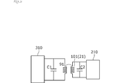
- FIG. 3 is a circuit diagram of the antenna device 101 and the counterpart antenna device coupled thereto.
- FIG. 4 is a four-sided view of the antenna device 102 according to the second embodiment.
- FIG. 5 is a four-sided view of the antenna device 103 according to the third embodiment.
- FIG. 6 is a four-side view of the antenna device 104 according to the fourth embodiment.
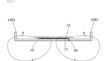
- FIG. 7 is a diagram illustrating a state of the magnetic flux ⁇ passing through the coil antenna 21 and the magnetic body 51.
- FIG. 8 is a four-sided view of the antenna device 105 according to the fifth embodiment.
- FIG. 9 is a diagram illustrating a state of the magnetic flux ⁇ passing through the coil antenna 21 and the magnetic body 52.
- FIGS. 10A, 10 ⁇ / b> B, 10 ⁇ / b> C, and 10 ⁇ / b> D are diagrams illustrating changes in characteristics of the antenna device 105 when the height of the bent portion at the end of the metal portion 10 is changed.
- 11A, 11 ⁇ / b> B, 11 ⁇ / b> C, and 11 ⁇ / b> D are diagrams illustrating changes in characteristics of the antenna device 105 when the width of the cutout formed in the bent portion at the end of the metal portion 10 is changed.
- FIG. 10A, 10 ⁇ / b> B, 10 ⁇ / b> C, and 10 ⁇ / b> D are diagrams illustrating changes in characteristics of the antenna device 105 when the width of the cutout formed in the bent portion at the end of the metal portion 10 is changed.
- FIG. 12 is a three-sided view of the antenna device 106 configured in an electronic apparatus including a housing that does not have the opening OP in the metal part 10.
- FIG. 13 is a three-side view of the antenna device 107 according to the seventh embodiment.
- FIG. 14 is a four-sided view of the antenna device 108 according to the eighth embodiment.
- FIG. 15 is a three-sided view of an antenna device 109A according to the ninth embodiment.
- FIG. 16 is a trihedral view of another antenna device 109B according to the ninth embodiment.
- FIG. 17 is a three-side view of the antenna device 110 according to the tenth embodiment.
- FIG. 18 is a three-sided view of the antenna device 111 according to the eleventh embodiment.
- FIG. 19 is a three-sided view of an antenna device 112A according to the twelfth embodiment.
- FIG. 20 is a trihedral view of another antenna device 112B according to the twelfth embodiment.
- FIG. 21 is a three-sided view of the antenna device 113 according to the thirteenth embodiment.
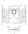
- FIG. 1 is a four-view diagram (plan view, left side view, right side view, front view) of an antenna device 101 according to the first embodiment.
- the antenna device 101 is configured as a portable electronic device (hereinafter simply referred to as “electronic device”).
- the plan view of FIG. 1 is a view (a plan view with the inside of the housing facing up) viewed from the inside of the housing of the electronic device. The same applies to the embodiments described below.
- the housing of the electronic device includes metal parts 10 and 11.
- the metal part 10 has a main surface that spreads in a planar shape.
- the metal part 10 is formed with a rectangular opening OP and a slit SL connecting the opening OP and one side. That is, the inner edge of the opening OP is continuous with the outer edge of the metal part 10.
- the metal parts 10 and 11 are formed by molding a metal plate made of aluminum, magnesium or an alloy thereof.
- the casing of the electronic device is formed by integrally forming the metal parts 10 and 11 and the resin part.
- the metal part 10 is an example of the “planar conductor” according to the present invention.
- the metal part 11 is not used as a component of the antenna device 101 but is used as a radiating element of another antenna.
- the rectangular antenna base 22 is formed with a coil antenna 21 made of a rectangular spiral coil conductor.
- the insulating base material 22 is a sheet of liquid crystal polymer (LCP) or polyimide resin (PI), for example, and the coil conductor is a Cu foil or the like formed on the insulating base material 22.
- the coil antenna 21 is obtained by patterning a Cu foil into a coil shape by photolithography or the like.
- a coil antenna sheet 20 is constituted by the insulating base material 22 and the coil antenna 21.
- the coil antenna sheet 20 is arranged on the metal part 10 so that the coil antenna 21 is along the inner edge of the opening OP of the metal part 10. Therefore, the coil antenna 21 having the coil conductor wound around the winding axis AX-AX and the metal portion 10 is coupled to at least a part of the coil antenna 21 when viewed in the direction of the winding axis.
- the antenna device 101 is constituted by the coil antenna 21 and the metal part 10 of the housing.
- the metal part 10 has bent parts 10B1 and 10B2 at the ends, and notches 10C1 and 10C2 are formed in the bent parts 10B1 and 10B2.
- the cutouts 10C1 and 10C2 are formed at portions of the bent portions 10B1 and 10B2 that intersect perpendicularly with the plane AS including the winding axis AX-AX.
- the notches 10C1 and 10C2 are formed on the surfaces of the bent portions 10B1 and 10B2 parallel to the winding axis AX-AX direction.
- the depths of the notches 10C1 and 10C2 reach the same position as the coil antenna 21 in the winding axis AX-AX direction.
- FIG. 1 also shows a coil antenna 91 that is a coupling partner.
- the coil antenna 21 and the coupling partner coil antenna 91 are magnetically coupled as indicated by a magnetic flux ⁇ .
- the magnetic flux ⁇ interlinking the coil antenna 21 is transmitted through the notches 10C1 and 10C2 of the metal part 10, so that the eddy current flowing through the metal part 10 is suppressed.
- the antenna device 101 having a high Q value and low loss can be obtained.
- FIG. 2 is a vertical cross-sectional view of the electronic device 201 on a plane passing through the metal part 10.
- the front unit 40 is provided with a display panel with a touch panel.
- a printed wiring board 30 is accommodated in the housing of the electronic device.
- the coil antenna sheet 20 is affixed to the inner surface of the metal part 10 via a double-sided adhesive sheet.
- the coil antenna 21 is connected to a circuit formed on the printed wiring board 30 via a spring pin 31.
- FIG. 3 is a circuit diagram of the antenna device 101 and the counterpart antenna device coupled thereto.
- a capacitor C2 is connected in parallel to the coil antenna 21 of the antenna device 101, and this parallel circuit is connected to the antenna connection circuit 210.
- the coil antenna 21 and the capacitor C2 constitute a parallel resonance circuit, and the resonance frequency thereof matches or approximates the use frequency band.
- a capacitor C1 is connected in parallel to the coil antenna 91 of the counterpart antenna device, and this parallel circuit is connected to the antenna connection circuit 310.
- the coil antenna 91 and the capacitor C1 constitute a parallel resonance circuit, and the resonance frequency thereof matches or approximates the use frequency band.
- the antenna connection circuits 210 and 310 are communication circuits.
- the frequency band used for NFC is, for example, the HF band, for example, 13.56 MHz.
- WPT Wireless Power Transmission
- the antenna connection circuit 210 is, for example, a power reception circuit
- the antenna connection circuit 310 is a power transmission circuit.
- the frequency band used for WPT is, for example, the HF band, for example, 6.78 MHz.
- the antenna device 101 can be applied to any WPT using magnetic field coupling such as an electromagnetic induction method, a magnetic field resonance method, and a direct current resonance method.
- Second Embodiment the structure from which the notch of a bending part differs from 1st Embodiment is shown.
- FIG. 4 is a four-sided view of the antenna device 102 according to the second embodiment.
- the configuration of the notches 10C1 and 10C2 formed in the bent portions 10B1 and 10B2 is different from the antenna device 101 shown in the first embodiment.
- a plurality of notches 10C1 and 10C2 are formed in the bent portions 10B1 and 10B2 of the metal portion 10, respectively.
- Other configurations are the same as those of the antenna device 101.
- shielding of the magnetic flux by the bent portions 10B1 and 10B2 of the metal portion 10 is further eliminated, and the eddy current flowing through the metal portion 10 due to the magnetic flux interlinking the coil antenna 21 is more effectively suppressed. .
- FIG. 5 is a four-sided view of the antenna device 103 according to the third embodiment.
- the configuration of the notches 10C1 and 10C2 formed in the bent portions 10B1 and 10B2 is different from the antenna device 101 shown in the first embodiment.
- the notches 10C1 and 10C2 have an inner portion that is wider than the edges of the bent portions 10B1 and 10B2. In other words, the opening at the notch is wide, but the width at the edge is narrow. Other configurations are the same as those of the antenna device 101.
- the magnetic flux is easily transmitted through the bent portions 10B1 and 10B2 of the metal portion 10, and the continuity of the edges of the bent portions 10B1 and 10B2 of the metal portion 10 can be maintained.
- the notches 10C1 and 10C2 may also serve as holes for providing functional parts such as some operation buttons, speakers, connectors, and sensors.
- FIG. 6 is a four-sided view of the antenna device 104 according to the fourth embodiment.
- This antenna device 104 is obtained by providing a magnetic body 51 to the antenna device 101 shown in the first embodiment.
- the magnetic body 51 is a rectangular magnetic ferrite sheet having an opening at the center.
- the opening of the magnetic body 51 has substantially the same size as the opening OP of the metal part 10 and overlaps in plan view. Other configurations are the same as those of the antenna device 101.
- FIG. 7 is a diagram illustrating a state of the magnetic flux ⁇ passing through the coil antenna 21 and the magnetic body 51.
- the magnetic flux interlinking the coil antenna 21 passes through the magnetic body 51 having a high permeability. That is, the magnetic body 51 acts as a magnetic path with a high magnetic permeability, suppresses unnecessary coupling with the printed wiring board, and increases the radiation effect and magnetic flux collection effect of the antenna device 104.
- FIG. 8 is a four-sided view of the antenna device 105 according to the fifth embodiment.
- This antenna device 105 is obtained by providing a magnetic body 52 to the antenna device 102 shown in the second embodiment.
- the magnetic body 52 is a magnetic ferrite sheet having an opening in part.
- the opening of the magnetic body 52 is substantially the same size as the opening OP of the metal part 10 and overlaps in plan view.
- the magnetic body 52 is a magnetic ferrite sheet having substantially the same size as the bottom surface of the metal portion 10. Accordingly, the two sides of the magnetic body 52 reach the vicinity of the bent portions 10B1 and 10B2 of the metal portion 10. Other configurations are the same as those of the antenna device 102.
- FIG. 9 is a diagram illustrating a state of the magnetic flux ⁇ passing through the coil antenna 21 and the magnetic body 52.
- the magnetic flux interlinking the coil antenna 21 passes through the magnetic body 52 having a high permeability. That is, the magnetic material acts as a magnetic path with high permeability. Since the magnetic body 52 exists in almost the entire bottom surface of the metal part 10, unnecessary coupling with the printed wiring board by the magnetic body 52 is suppressed, and the effect of radiation and magnetic collection of the magnetic flux of the antenna device 105 is high.
- the end portion of the magnetic body 52 is close to the bent portions 10B1 and 10B2 of the metal portion 10, so that the magnetic flux ⁇ passing through the magnetic body 52 is easily transmitted through the notches 10C1 and 10C2. That is, the effect by providing these notches 10C1 and 10C2 is great.
- FIG. 10A shows the inductance L of the antenna device when the coil antenna 21 side is viewed from the circuit connected to the coil antenna 21.
- FIG. 10B shows the resistance R value of the antenna device
- FIG. 10C shows the Q value of the antenna device
- FIG. 10D shows the coupling coefficient k with the coil antenna of the coupling partner.
- the resistance R value is maximum when the height of the bent portions 10B1 and 10B2 is 0.5 mm, and even when the height is higher than that, there is no bent portion (0 mm).
- the resistance R value is high.
- the Q value is minimum when the height of the bent portions 10B1 and 10B2 is 0.5 mm, and compared with the state where there is no bent portion (0 mm) even if the height is further increased. Q value is low.
- 11A, 11B, 11C, and 11D show the width dependency of the notch formed in the bent portion of the end portion of the metal portion 10, that is, the cut formed in the bent portion of the end portion of the metal portion 10. It is a figure which shows the characteristic change of the antenna apparatus 105 when changing the width
- the antenna device illustrated here is the antenna device 105 shown in FIG. 8, the metal portion 10 is 130 mm in the vertical direction and 70 mm in the left and right, and the height of the bent portions 10B1 and 10B2 and the depth of the notches 10C1 and 10C2 are as described above.
- the antenna device has a structure in which the width of the cutouts 10C1 and 10C2 and the interval between the cutouts and the cutouts are made equal to each other, fixed at 0.5 mm.
- the Q value is maximum when the notch width and the interval between the notch and the notch are 1 mm, and the Q value is substantially constant even if it is wider than that. From this, it can be seen that there is an effect of improving the Q value only by forming a notch having a narrow width compared to the length of the metal portion 10. This also indicates that an antenna device with a high Q value and a low loss can be obtained without substantially reducing the rigidity of the housing.
- FIG. 12 is a three-view diagram (plan view, left side view, right side view) of the antenna device 106 configured in an electronic apparatus including a housing that does not have the opening OP in the metal part 10.
- the housing of the electronic device provided with the antenna device 106 includes the metal part 10 and the resin parts 61 and 62.
- the metal part 10 does not have the opening OP as shown in FIG.
- the coil antenna sheet 20 is affixed at a position where at least a part of the opening of the coil antenna 21 protrudes from the metal part 10. With this structure, the coil antenna 21 is not shielded by the metal part 10.
- Cutouts 10C1 and 10C2 are formed in the bent portions 10B1 and 10B2 of the metal portion 10. Since the magnetic flux ⁇ interlinked with the coil antenna 21 passes through the notches 10C1 and 10C2, the antenna device 106 having a high Q value and low loss can be obtained.
- FIG. 12 shows an example in which the coil antenna 21 overlaps the metal part 10 (planar conductor) in a plan view.
- the coil antenna 21 may be a metal as long as it is coupled to the metal part 10 (planar conductor). It may be at a position away from the portion 10 (planar conductor) in plan view. Therefore, for example, they may be close to each other at a distance less than the outer width of the coil antenna 21 (preferably, less than half the outer width of the coil antenna 21).
- an antenna device configured in an electronic apparatus including a housing that does not have a slit SL in a metal portion is shown.
- FIG. 13 is a three-side view of the antenna device 107 according to the seventh embodiment.
- the housing of the electronic apparatus provided with the antenna device 107 includes a metal part 10 and a resin part 61.
- the metal part 10 does not have the slit SL as shown in FIG. 1, and one side of the opening OP is open to the outer edge.
- the coil antenna sheet 20 is affixed at a position where the opening of the coil antenna 21 overlaps the opening OP of the metal part 10. With this structure, the coil antenna 21 is not shielded by the metal part 10.
- FIG. 14 is a four-sided view of the antenna device 108 according to the eighth embodiment.
- the antenna device 108 is configured as an electronic device.
- the housing of the electronic device includes a metal part 10.
- the metal part 10 has a main surface that spreads in a planar shape.
- the metal part 10 is formed with a rectangular opening OP and a slit SL connecting the opening OP and one side. That is, the inner edge of the opening OP is continuous with the outer edge of the metal part 10.
- the rectangular antenna base 22 is formed with a coil antenna 21 made of a rectangular spiral coil conductor.
- a coil antenna sheet 20 is constituted by the insulating base material 22 and the coil antenna 21.
- the antenna device 101 includes the coil antenna 21 and the metal part 10 of the housing. This configuration is as shown in the first embodiment and the like.
- the metal part 10 of the present embodiment has a bent part 10B that is non-perpendicular to the main surface of the metal part 10 at the end. Notches 10C1, 10C2, 10C3, and 10C4 are formed in the bent portion 10B. The notches 10C1, 10C2, 10C3, and 10C4 are respectively formed at portions of the bent portion 10B that intersect perpendicularly with the plane AS that includes the winding axis AX-AX.
- the density of the magnetic flux that intersects at the above portion of the magnetic flux interlinking the coil antenna 21 is high. That is, eddy currents are likely to occur at this location. However, the eddy current is effectively suppressed by providing the notches 10C1, 10C2, 10C3, and 10C4 at this location.
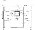
- FIG. 15 is a three-sided view of the antenna device 109A according to the ninth embodiment.
- the configuration of the notches 10C1 and 10C2 formed in the bent portions 10B1 and 10B2 is different from the antenna device 101 shown in the first embodiment.
- the width W of the notches 10C1 and 10C2 along the bent portions 10B1 and 10B2 is larger than the width (diameter) D of the coil antenna 21.
- Other configurations are the same as those of the antenna device 101.
- FIG. 16 is a three-view drawing of another antenna device 109B according to the ninth embodiment.
- the ends of the notches 10C1 and 10C2 reach the end in the direction along the bent portions 10B1 and 10B2.
- shielding of the magnetic flux by the bent portions 10B1 and 10B2 of the metal portion 10 is further eliminated, and the eddy current flowing through the metal portion 10 due to the magnetic flux interlinking the coil antenna 21 is more effectively suppressed. .
- the tenth embodiment shows an example in which the shape of the metal part of the housing is different from that of the first embodiment.
- FIG. 17 is a three-sided view of the antenna device 110 according to the tenth embodiment.
- the shape of the metal part 11 and the notches 10C1 and 10C2 of the housing is different from the antenna device 101 shown in the first embodiment.
- a slit SL2 is formed between the metal parts 10 and 11 of the housing, and the slit SL2 extends in a non-perpendicular direction with respect to the boundary between the plane and the side surface.
- FIG. 18 is a three-sided view of the antenna device 111 according to the eleventh embodiment.
- the size of the notches 10C1 and 10C2 formed in the bent portions 10B1 and 10B2 is different from the antenna device 103 shown in the third embodiment.
- the spread width W of the notches 10C1 and 10C2 inside the bent portions 10B1 and 10B2 is larger than the width (diameter) D of the coil antenna 21.
- an opening 10D is formed at a position adjacent to the notch 10C2.
- the opening 10D is provided with functional parts such as operation buttons, a speaker, a connector such as an earphone jack and a power supply, and a card slot.
- FIG. 19 is a three-sided view of the antenna device 112A according to the twelfth embodiment.
- the width W of the notches 10C1 and 10C2 inside the bent portions 10B1 and 10B2 extends over almost the entire length of the metal portion 10 of the housing.
- FIG. 20 is a three-sided view of another antenna device 112B according to the twelfth embodiment.
- the widths W of the notches 10C1 and 10C2 in the bent portions 10B1 and 10B2 are sufficiently wider than the remaining width.
- the width of the notches 10C1 and 10C2 may be as wide as possible.
- FIG. 21 is a three-sided view of the antenna device 113 according to the thirteenth embodiment.
- the depth B of the notches 10C1 and 10C2 formed in the bent portions 10B1 and 10B2 of the metal portion 10 is shallower than the height H of the bent portions 10B1 and 10B2.
- Other basic configurations are the same as those of the antenna device 101.
- the casing since the casing has high rigidity, it has high resistance to external force.
- the coil antenna 21 is combined with the main surface of the planar conductor to enhance the effect of magnetic flux radiation and magnetic collection.
- the coil antenna 21 is a planar conductor. There is no direct relationship with the radiation of magnetic flux and the effect of magnetic collection by coupling with the main surface of the magnetic field.
- the present invention suppresses an increase in the resistance value and a decrease in the Q value of the antenna device caused by having a bend at the end of the planar conductor by providing a notch in the bent portion at the end of the planar conductor. Is. Therefore, the planar conductor may not have an effect of increasing radiation and magnetism.
Landscapes
- Aerials With Secondary Devices (AREA)
- Support Of Aerials (AREA)
Abstract
アンテナ装置は、巻回軸AX-AX周りに巻回されたコイル導体を有するコイルアンテナ(21)と、巻回軸AX-AXの方向に平面視したとき、コイルアンテナ(21)の少なくとも一部と結合する面を有する金属部(10)と、を備える。金属部(10)は、端部に曲げ部(10B1,10B2)を有する。曲げ部(10B1,10B2)には切り欠き(10C1,10C2)が形成されている。これにより、アンテナ装置の特性劣化が抑制される。
Description
本発明は、コイルアンテナを有するアンテナ装置に関し、特に平面導体と共に用いられるアンテナ装置およびそれを備える電子機器に関する。
コイルアンテナを面状導体に結合させることにより、磁束を効率よく放射させるアンテナ装置が特許文献1に示されている。このように、コイルアンテナによるアンテナ装置を、面状導体を備える電子機器に設ける場合に、面状導体がコイルアンテナの磁束を遮蔽しないように設けることによって、電子機器にアンテナ装置を容易に組み込むことができる。
一般に、金属筐体等を備えた携帯電子機器においては、内部空間を大きくしつつ剛性を高めるため、金属筐体の端部は曲がっている場合が多い。本願発明者等は、このような端部が曲がっている金属筐体とコイルアンテナとを備えるアンテナ装置を構成した場合に金属筐体の形状がアンテナの特性に大きな影響を及ぼすことを見出した。すなわち、コイルアンテナを鎖交する磁束が金属筐体の曲がった端部を抜けようとする際に、金属筐体に強い渦電流が流れる。このことが、アンテナ装置のQ値の低下、損失の増大、といった特性劣化の一つの原因であることを見出した。
本発明の目的は、上述のアンテナ装置の特性劣化が抑制されるようにしたアンテナ装置およびそれを備える電子機器を提供することにある。
(1)本発明のアンテナ装置は、巻回軸の周りに巻回されたコイル導体を有するコイルアンテナと、前記巻回軸の方向に平面視したとき、前記コイルアンテナの少なくとも一部と結合する主面を有する面状導体と、を備え、
前記面状導体は、前記主面の端部に曲げ部を有し、前記曲げ部に切り欠きが形成されたことを特徴とする。
前記面状導体は、前記主面の端部に曲げ部を有し、前記曲げ部に切り欠きが形成されたことを特徴とする。
上記構成により、コイルアンテナを鎖交する磁束が、面状導体の切り欠きを透過することで、面状導体に流れる渦電流が抑制される。その結果、Q値が高く、低損失のアンテナ装置が得られる。
(2)上記(1)において、前記コイルアンテナは、前記巻回軸の方向に平面視したとき、前記面状導体の主面と重なる磁性体を有することが好ましい。これにより、磁性体は高透磁率の磁路として作用し、集磁効果が高まる。磁性体を抜ける磁束が面状導体の曲げ部に近いほど、磁束は切り欠きを透過しやすくなるので、この切り欠きを設けることによる効果は増大する。
(3)上記(1)(2)において、前記切り欠きは、前記曲げ部のうち、前記巻回軸を含む平面と垂直に交わる箇所に形成されることが好ましい。これにより、面状導体の曲げ部において磁束の透過を最も遮る位置に切り欠きが形成されることになるので、その切り欠きを設けることによる効果は大きい。
(4)上記(1)から(3)のいずれかにおいて、前記切り欠きは、複数個形成されていることが好ましい。これにより、面状導体の端部による磁束の遮蔽がより解消される。
(5)上記(1)から(4)のいずれかにおいて、前記切り欠きの深さは、前記巻回軸の方向において前記コイルアンテナと同じ位置に達する深さであることが好ましい。このことにより、面状導体の曲げ部において磁束が透過しやすい高さ位置に切り欠きが形成されることになるので、その切り欠きを設けることによる効果は大きい。
(6)本発明の電子機器は、
筐体内にアンテナ装置が構成された、または筐体と共にアンテナ装置が構成され、
前記アンテナ装置は、
巻回軸の周りに巻回されたコイル導体を有するコイルアンテナと、前記巻回軸の方向に平面視したとき、前記コイルアンテナの少なくとも一部と結合する主面を有する面状導体と、を備え、
前記面状導体は、前記主面の端部に曲げ部を有し、前記曲げ部に切り欠きが形成されたことを特徴とする。
筐体内にアンテナ装置が構成された、または筐体と共にアンテナ装置が構成され、
前記アンテナ装置は、
巻回軸の周りに巻回されたコイル導体を有するコイルアンテナと、前記巻回軸の方向に平面視したとき、前記コイルアンテナの少なくとも一部と結合する主面を有する面状導体と、を備え、
前記面状導体は、前記主面の端部に曲げ部を有し、前記曲げ部に切り欠きが形成されたことを特徴とする。
上記構成により、Q値が高く、低損失のアンテナ装置を備える電子機器が得られる。
本発明によれば、面状導体の端部を透過する磁束が遮蔽されにくくなって、Q値が高く、低損失のアンテナ装置、およびそれを備える電子器が得られる。
以降、図を参照して幾つかの具体的な例を挙げて、本発明を実施するための複数の形態を示す。各図中には同一箇所に同一符号を付している。要点の説明または理解の容易性を考慮して、便宜上実施形態を分けて示すが、異なる実施形態で示した構成の部分的な置換または組み合わせが可能である。第2の実施形態以降では第1の実施形態と共通の事柄についての記述を省略し、異なる点についてのみ説明する。特に、同様の構成による同様の作用効果については実施形態毎には逐次言及しない。
《第1の実施形態》
図1は第1の実施形態に係るアンテナ装置101の四面図(平面図、左側面図、右側面図、正面図)である。このアンテナ装置101は携帯電子機器(以下、単に「電子機器」)に構成される。図1の平面図は、電子機器の筐体の内側から視た図(筐体の内側を上面にした状態での平面図)である。このことは以降に示す各実施形態についても同様である。
図1は第1の実施形態に係るアンテナ装置101の四面図(平面図、左側面図、右側面図、正面図)である。このアンテナ装置101は携帯電子機器(以下、単に「電子機器」)に構成される。図1の平面図は、電子機器の筐体の内側から視た図(筐体の内側を上面にした状態での平面図)である。このことは以降に示す各実施形態についても同様である。
電子機器の筐体は金属部10,11を含む。金属部10は面状に広がる主面を有する。金属部10には、方形の開口OPおよび、この開口OPと一辺との間を繋ぐスリットSLが形成されている。すなわち、開口OPの内縁は金属部10の外縁に連続している。
金属部10,11は、アルミニウム、マグネシウムまたはこれらの合金による金属板を成形したものである。電子機器の筐体は、これら金属部10,11と樹脂部とが一体成形されたものである。上記金属部10は本発明に係る「面状導体」の一例である。金属部11は、アンテナ装置101の構成要素としては用いられず、別のアンテナの放射素子として用いられる。
方形の絶縁性基材22には、矩形スパイラル状のコイル導体によるコイルアンテナ21が形成されている。絶縁性基材22は例えば液晶ポリマー(LCP)やポリイミド樹脂(PI)等のシートであり、コイル導体は絶縁性基材22に形成されたCu箔等である。コイルアンテナ21はCu箔がフォトリソグラフィ等によってコイル状にパターン化されたものである。絶縁性基材22およびコイルアンテナ21によってコイルアンテナシート20が構成されている。
コイルアンテナシート20は、コイルアンテナ21が金属部10の上記開口OPの内縁に沿うように、金属部10に配置されている。したがって、巻回軸AX-AX周りに巻回されたコイル導体を有するコイルアンテナ21と、巻回軸の方向に平面視したとき、金属部10はコイルアンテナ21の少なくとも一部と結合する。このように、上記コイルアンテナ21と筐体の金属部10とでアンテナ装置101は構成されている。
金属部10は、端部に曲げ部10B1,10B2を有し、曲げ部10B1,10B2に切り欠き10C1,10C2が形成されている。切り欠き10C1,10C2は、曲げ部10B1,10B2のうち、巻回軸AX-AXを含む平面ASと垂直に交わる箇所に形成されている。言い換えると、切り欠き10C1,10C2は、曲げ部10B1,10B2のうち、巻回軸AX-AX方向に平行な面に形成されている。また、切り欠き10C1,10C2の深さは、巻回軸AX-AX方向においてコイルアンテナ21と同じ位置に達する。
図1では、結合相手のコイルアンテナ91も示している。コイルアンテナ21と結合相手のコイルアンテナ91とは、磁束φで示すように、磁界結合する。コイルアンテナ21を鎖交する磁束φは、金属部10の切り欠き10C1,10C2を透過することで、金属部10に流れる渦電流が抑制される。その結果、Q値が高く、低損失のアンテナ装置101が得られる。
図2は、電子機器201の、金属部10を通る面での縦断面図である。前面ユニット40にはタッチパネル付きディスプレイパネルが設けられている。電子機器の筐体内にはプリント配線板30が収容されている。コイルアンテナシート20は、金属部10の内面に両面粘着シートを介して貼付されている。コイルアンテナ21は、スプリングピン31を介して、プリント配線板30に形成されている回路に接続される。
図3は、アンテナ装置101および、それに結合する相手側アンテナ装置の回路図である。アンテナ装置101のコイルアンテナ21にはキャパシタC2が並列接続され、この並列回路がアンテナ接続回路210に接続されている。コイルアンテナ21とキャパシタC2とは並列共振回路を構成し、その共振周波数は使用周波数帯に一致または近似する。相手側アンテナ装置のコイルアンテナ91にはキャパシタC1が並列接続され、この並列回路がアンテナ接続回路310に接続されている。コイルアンテナ91とキャパシタC1とは並列共振回路を構成し、その共振周波数は使用周波数帯に一致または近似する。
例えば、図3に示した回路をNFC(NearField Communication)に用いる場合は、アンテナ接続回路210,310は通信回路である。NFCの使用周波数帯は例えばHF帯であり、例えば13.56MHzである。WPT(Wireless Power Transmission)に用いる場合は、アンテナ接続回路210は例えば電力受電回路であり、アンテナ接続回路310は電力送電回路である。WPTの使用周波数帯は例えばHF帯であり、例えば6.78MHzである。このアンテナ装置101は、電磁誘導方式、磁界共鳴方式、および直流共鳴方式等の磁界結合を利用したいずれのWPTにも適用できる。
《第2の実施形態》
第2の実施形態では、曲げ部の切り欠きの構成が第1の実施形態とは異なる例を示す。
第2の実施形態では、曲げ部の切り欠きの構成が第1の実施形態とは異なる例を示す。
図4は第2の実施形態に係るアンテナ装置102の四面図である。第1の実施形態で示したアンテナ装置101とは、曲げ部10B1,10B2に形成された切り欠き10C1,10C2の構成が異なる。本実施形態のアンテナ装置102においては、金属部10の曲げ部10B1,10B2に、それぞれ複数の切り欠き10C1,10C2が形成されている。その他の構成はアンテナ装置101と同じである。
本実施形態によれば、金属部10の曲げ部10B1,10B2による磁束の遮蔽がより解消され、コイルアンテナ21を鎖交する磁束による、金属部10に流れる渦電流はより効果的に抑制される。
《第3の実施形態》
第3の実施形態では、曲げ部の切り欠きの構成が第1の実施形態とは異なる例を示す。
第3の実施形態では、曲げ部の切り欠きの構成が第1の実施形態とは異なる例を示す。
図5は第3の実施形態に係るアンテナ装置103の四面図である。第1の実施形態で示したアンテナ装置101とは、曲げ部10B1,10B2に形成された切り欠き10C1,10C2の構成が異なる。本実施形態のアンテナ装置103においては、切り欠き10C1,10C2は曲げ部10B1,10B2の縁より内部が拡がっている。言い換えると、切り欠きによる開口は広いながらも、縁での幅は狭い。その他の構成はアンテナ装置101と同じである。
本実施形態によれば、金属部10の曲げ部10B1,10B2で磁束は透過し易く、且つ金属部10の曲げ部10B1,10B2の縁の連続性を維持できる。また、このような切り欠き10C1,10C2は、何らかの操作ボタン、スピーカー、コネクタ、センサ等の機能部品を設けるための穴を兼ねてもよい。
《第4の実施形態》
第4の実施形態では磁性体を備えるアンテナ装置の例を示す。
第4の実施形態では磁性体を備えるアンテナ装置の例を示す。
図6は第4の実施形態に係るアンテナ装置104の四面図である。このアンテナ装置104は、第1の実施形態で示したアンテナ装置101に磁性体51を設けたものである。磁性体51は中央に開口を有する方形の磁性体フェライトシートである。この磁性体51の開口は金属部10の開口OPとほぼ同じ大きさで且つ平面視で重なる。その他の構成はアンテナ装置101と同じである。
図7は、コイルアンテナ21および磁性体51を通る磁束φの様子を示す図である。コイルアンテナ21を鎖交する磁束は高透磁率の磁性体51を通る。すなわち、磁性体51は高透磁率の磁路として作用し、プリント配線板との不要な結合を抑制し、アンテナ装置104の磁束の放射および集磁の効果が高まる。
《第5の実施形態》
第5の実施形態では、第4の実施形態のアンテナ装置とは磁性体の大きさが異なり、第1の実施形態とは曲げ部の切り欠きの構成が異なる、アンテナ装置の例を示す。
第5の実施形態では、第4の実施形態のアンテナ装置とは磁性体の大きさが異なり、第1の実施形態とは曲げ部の切り欠きの構成が異なる、アンテナ装置の例を示す。
図8は第5の実施形態に係るアンテナ装置105の四面図である。このアンテナ装置105は、第2の実施形態で示したアンテナ装置102に磁性体52を設けたものである。磁性体52は一部に開口を有する磁性体フェライトシートである。この磁性体52の開口は金属部10の開口OPとほぼ同じ大きさで且つ平面視で重なる。磁性体52は金属部10の底面とほぼ同じ大きさの磁性体フェライトシートである。したがって、磁性体52の2辺は金属部10の曲げ部10B1,10B2の近傍に達する。その他の構成はアンテナ装置102と同じである。
図9は、コイルアンテナ21および磁性体52を通る磁束φの様子を示す図である。コイルアンテナ21を鎖交する磁束は高透磁率の磁性体52を通る。すなわち、磁性体は高透磁率の磁路として作用する。磁性体52は金属部10の底面のほぼ全域に存在するので、磁性体52によるプリント配線板との不要な結合を抑制し、アンテナ装置105の磁束の放射および集磁の効果は高い。図7に示した例とは異なり、磁性体52の端部は、金属部10の曲げ部10B1,10B2に近いので、磁性体52を抜ける磁束φは切り欠き10C1,10C2を透過しやすくなる。つまり、この切り欠き10C1,10C2を設けることによる効果は大きい。
図10(A)(B)(C)(D)は、金属部10の端部の曲げ部の高さ依存性、すなわち、金属部10の端部の曲げ部の高さを変えたときのアンテナ装置105の特性変化を示す図である。ここで例示するアンテナ装置は、図8に示したアンテナ装置105において、切り欠き10C1,10C2を形成しない構造のアンテナ装置である。図10(A)(B)(C)(D)のいずれも、横軸は曲げ部10B1,10B2の高さである。図10(A)はコイルアンテナ21に接続された回路からコイルアンテナ21側を視たアンテナ装置のインダクタンスLである。図10(B)はアンテナ装置の抵抗R値、図10(C)はアンテナ装置のQ値、図10(D)は結合相手のコイルアンテナとの結合係数kである。
図10(B)に表れているように、曲げ部10B1,10B2の高さが0.5mmで抵抗R値は最大となり、それ以上高くなっても曲げ部が無い(0mm)状態と比較して抵抗R値は高い。また、図10(C)に表れているように、曲げ部10B1,10B2の高さが0.5mmでQ値は最低となり、それ以上高くなっても曲げ部が無い(0mm)の状態と比較してQ値は低い。
図11(A)(B)(C)(D)は、金属部10の端部の曲げ部に形成する切り欠きの幅依存性、すなわち、金属部10の端部の曲げ部に形成する切り欠きの幅を変えたときのアンテナ装置105の特性変化を示す図である。ここで例示するアンテナ装置は、図8に示したアンテナ装置105において、金属部10は上下を130mm、左右を70mmとし、曲げ部10B1,10B2の高さおよび切り欠き10C1,10C2の深さを上記0.5mmに固定し、切り欠き10C1,10C2の幅と、切り欠きと切り欠きとの間隔とを等しくした構造のアンテナ装置である。
図11(C)に表れているように、Q値は切り欠き幅および切り欠きと切り欠きとの間隔が1mmで最大となり、それ以上広くてもQ値はほぼ一定である。このことから、金属部10の長さに比較して狭幅の切り欠きを形成するだけで、Q値向上効果があることが分かる。また、このことから、筐体の剛性を殆ど低下させることなく、Q値の高い、低損失のアンテナ装置が得られることが分かる。
《第6の実施形態》
第6の実施形態では、金属部に開口を有しない筐体を備える電子機器に構成されるアンテナ装置について示す。
第6の実施形態では、金属部に開口を有しない筐体を備える電子機器に構成されるアンテナ装置について示す。
図12は、金属部10に開口OPを有しない筐体を備える電子機器に構成されるアンテナ装置106の三面図(平面図、左側面図、右側面図)である。このアンテナ装置106が設けられる電子機器の筐体は金属部10と樹脂部61,62とを備える。金属部10には、図1に示したような開口OPは無い。コイルアンテナシート20は、コイルアンテナ21の開口の少なくとも一部が金属部10よりはみ出る位置に貼付されている。この構造により、コイルアンテナ21は金属部10に遮蔽されない。
金属部10の曲げ部10B1,10B2には切り欠き10C1,10C2が形成されている。コイルアンテナ21と鎖交する磁束φは切り欠き10C1,10C2を透過するので、Q値が高く、低損失のアンテナ装置106が得られる。
なお、図12では、コイルアンテナ21が金属部10(面状導体)に平面視で重なる例を示したが、コイルアンテナ21は金属部10(面状導体)と結合する程度であれば、金属部10(面状導体)から平面視で離れた位置にあってもよい。したがって、例えばコイルアンテナ21の外形幅未満(好ましくは、コイルアンテナ21の外形幅の1/2未満)の距離で近接していてもよい。
《第7の実施形態》
第7の実施形態では、金属部にスリットSLを有しない筐体を備える電子機器に構成されるアンテナ装置について示す。
第7の実施形態では、金属部にスリットSLを有しない筐体を備える電子機器に構成されるアンテナ装置について示す。
図13は第7の実施形態に係るアンテナ装置107の三面図である。このアンテナ装置107が設けられる電子機器の筐体は金属部10と樹脂部61とを備える。金属部10には、図1に示したようなスリットSLは無く、開口OPの一辺が外縁に開いている。コイルアンテナシート20は、コイルアンテナ21の開口が金属部10の開口OPに重なる位置に貼付されている。この構造により、コイルアンテナ21は金属部10に遮蔽されない。
《第8の実施形態》
第8の実施形態では、非垂直に曲げられた曲げ部10Bを有する金属部を備えるアンテナ装置について示す。
第8の実施形態では、非垂直に曲げられた曲げ部10Bを有する金属部を備えるアンテナ装置について示す。
図14は第8の実施形態に係るアンテナ装置108の四面図である。このアンテナ装置108は電子機器に構成される。電子機器の筐体は金属部10を含む。金属部10は面状に広がる主面を有する。金属部10には、方形の開口OPおよび、この開口OPと一辺との間を繋ぐスリットSLが形成されている。すなわち、開口OPの内縁は金属部10の外縁に連続している。
方形の絶縁性基材22には、矩形スパイラル状のコイル導体によるコイルアンテナ21が形成されている。絶縁性基材22およびコイルアンテナ21によってコイルアンテナシート20が構成されている。
コイルアンテナ21と筐体の金属部10とでアンテナ装置101は構成されている。この構成は、第1の実施形態等で示したとおりである。
本実施形態の金属部10は、端部に、金属部10の主面に対して非垂直の曲げ部10Bが形成されている。この曲げ部10Bに切り欠き10C1,10C2,10C3,10C4が形成されている。切り欠き10C1,10C2,10C3,10C4は、曲げ部10Bのうち、巻回軸AX-AXを含む平面ASと垂直に交わる箇所にそれぞれ形成されている。
曲げ部10Bのうち、コイルアンテナ21の巻回軸AX-AXを含む平面ASと垂直に交わる箇所においては、コイルアンテナ21を鎖交する磁束のうち、上記箇所で交わる磁束の密度が高い。すなわち、この箇所で渦電流が発生しやすい。しかし、この箇所に切り欠き10C1,10C2,10C3,10C4が設けられることにより、渦電流は効果的に抑制される。
《第9の実施形態》
第9の実施形態では、曲げ部の切り欠きの構成が第1の実施形態とは異なる例を示す。
第9の実施形態では、曲げ部の切り欠きの構成が第1の実施形態とは異なる例を示す。
図15は第9の実施形態に係るアンテナ装置109Aの三面図である。第1の実施形態で示したアンテナ装置101とは、曲げ部10B1,10B2に形成された切り欠き10C1,10C2の構成が異なる。本実施形態のアンテナ装置109Aにおいては、曲げ部10B1,10B2に沿った切り欠き10C1,10C2の幅Wが、コイルアンテナ21の幅(径)Dより大きい。その他の構成はアンテナ装置101と同じである。
図16は第9の実施形態に係る別のアンテナ装置109Bの三面図である。この例では、更に、切り欠き10C1,10C2の一端が、曲げ部10B1,10B2に沿う方向で端部にまで達している。
本実施形態によれば、金属部10の曲げ部10B1,10B2による磁束の遮蔽がより解消され、コイルアンテナ21を鎖交する磁束による、金属部10に流れる渦電流はより効果的に抑制される。
《第10の実施形態》
第10の実施形態では、筐体の金属部の形状が第1の実施形態とは異なる例を示す。
第10の実施形態では、筐体の金属部の形状が第1の実施形態とは異なる例を示す。
図17は第10の実施形態に係るアンテナ装置110の三面図である。第1の実施形態で示したアンテナ装置101とは、筐体の金属部11および切り欠き10C1,10C2の形状が異なる。筐体の金属部10と11との間にスリットSL2が形成されているが、このスリットSL2は、平面と側面との境界に対して非垂直方向に延伸している。
本実施形態によれば、筐体の金属部10,11との間に形成されるスリットSL2による美観が優れる。また、筐体全体の剛性が高いため、外力に対する耐性が高い。
《第11の実施形態》
第11の実施形態では、曲げ部の切り欠きの構成が第3の実施形態とは異なる例を示す。
第11の実施形態では、曲げ部の切り欠きの構成が第3の実施形態とは異なる例を示す。
図18は第11の実施形態に係るアンテナ装置111の三面図である。第3の実施形態で示したアンテナ装置103とは、曲げ部10B1,10B2に形成された切り欠き10C1,10C2の大きさが異なる。本実施形態のアンテナ装置111においては、切り欠き10C1,10C2の、曲げ部10B1,10B2内部での拡がり幅Wが、コイルアンテナ21の幅(径)Dより大きい。
また、アンテナ装置111では、筐体の金属部10の両側部に形成される切り欠き10C1,10C2は左右非対称である。切り欠き10C2は切り欠き10C1より小さい。切り欠き10C2には例えば操作ボタン70、スピーカー、イヤホンジャックや電源等のコネクタ、カードスロット等の機能部品が配置される。
また、アンテナ装置111では、切り欠き10C2に隣接する位置に開口10Dが形成されている。この開口10Dにも同様に、例えば操作ボタン、スピーカー、イヤホンジャックや電源等のコネクタ、カードスロット等の機能部品が設けられる。
《第12の実施形態》
第12の実施形態では、曲げ部の切り欠きの構成が第1、第3の実施形態とは異なる例を示す。
第12の実施形態では、曲げ部の切り欠きの構成が第1、第3の実施形態とは異なる例を示す。
図19は第12の実施形態に係るアンテナ装置112Aの三面図である。アンテナ装置112Aにおいては、切り欠き10C1,10C2の、曲げ部10B1,10B2内部での拡がり幅Wが、筐体の金属部10のほぼ全長に亘っている。
図20は第12の実施形態に係る別のアンテナ装置112Bの三面図である。アンテナ装置112Bにおいては、曲げ部10B1,10B2における切り欠き10C1,10C2の幅Wは残余の幅より充分に広い。
このように、切り欠き10C1,10C2の幅は可能な限り広くしてもよい。
《第13の実施形態》
第13の実施形態では、曲げ部の切り欠きの構成が第1の実施形態とは異なる例を示す。
第13の実施形態では、曲げ部の切り欠きの構成が第1の実施形態とは異なる例を示す。
図21は第13の実施形態に係るアンテナ装置113の三面図である。このアンテナ装置113においては、金属部10の曲げ部10B1,10B2に形成される切り欠き10C1,10C2の深さBは曲げ部10B1,10B2の高さHより浅い。その他の基本的な構成はアンテナ装置101と同じである。
以上の各実施形態では、切り欠き10C1,10C2の深さが、巻回軸AX-AX方向においてコイルアンテナ21と同じ位置に達する深さである例を示したが、本実施形態のように、切り欠き10C1,10C2の深さがコイルアンテナ21と同じ位置に達せず、浅くても渦電流を抑制する効果はある。但し、切り欠き10C1,10C2の深さが、巻回軸AX-AX方向においてコイルアンテナ21と同じ位置に達する深さ以上とすることで、コイルアンテナ21と鎖交する磁束が交わることを抑制し、渦電流をより抑制する効果がある。
本実施形態によれば、筐体の剛性が高いため、外力に対する耐性が高い。
《他の実施形態》
以上に示した各実施形態では、金属部10の端部に平面的に屈曲した曲げ部を形成した例を示したが、この曲げ部は所定曲率で湾曲していてもよい。
以上に示した各実施形態では、金属部10の端部に平面的に屈曲した曲げ部を形成した例を示したが、この曲げ部は所定曲率で湾曲していてもよい。
また、以上の各実施形態では、切り欠き(10C1,10C2等)が、曲げ部(10B1,10B2等)のうち、コイルアンテナ21の巻回軸AX-AXを含む平面と垂直に交わる箇所に形成された例を示したが、切り欠きは、コイルアンテナ21の巻回軸AX-AXを含む平面と交わる箇所であればよい。但し、上述のとおり、曲げ部のうち、コイルアンテナ21の巻回軸AX-AXを含む平面と垂直に交わる箇所においては、コイルアンテナ21を鎖交する磁束のうち、上記箇所で交わる磁束の密度が高い。すなわち、この箇所に切り欠きが設けられることで渦電流抑制効果が高まる。
また、以上の各実施形態では、金属部の2つの端部に曲げ部を有し、いずれの曲げ部にも切り欠きを設けた例を示したが、一方の曲げ部にのみ切り欠きを設けてもよい。
また、以上の各実施形態では、電子機器の筐体の一部である金属部10をアンテナ装置の面状導体として利用したが、筐体内に収容されるシールドケースやバッテリパック等の導体部材が面状導体であってもよい。
なお、以上の各実施形態では、コイルアンテナ21が面状導体の主面と結合することにより、磁束の放射および集磁の効果を高めているが、本発明は、コイルアンテナ21が面状導体の主面と結合することによる磁束の放射および集磁の効果とは直接関係は無い。本発明は面状導体の端部の曲げ部に切り欠きを設けることにより、面状導体の端部に曲げ部を有することに起因するアンテナ装置の抵抗値の上昇やQ値の低下を抑制するものである。よって、面状導体が放射および集磁を高める効果を有していなくてもよい。
最後に、上述の実施形態の説明は、すべての点で例示であって、制限的なものではない。当業者にとって変形および変更が適宜可能である。本発明の範囲は、上述の実施形態ではなく、特許請求の範囲によって示される。さらに、本発明の範囲には、特許請求の範囲内と均等の範囲内での実施形態からの変更が含まれる。
AX…巻回軸
C1,C2…キャパシタ
OP…開口
SL,SL2…スリット
10,11…筐体の金属部(面状導体)
11…筐体の金属部
10B1,10B2…曲げ部
10C1,10C2…切り欠き
10D…開口
20…コイルアンテナシート
21…コイルアンテナ
22…絶縁性基材
30…プリント配線板
31…スプリングピン
40…前面ユニット
51,52…磁性体
61,62…樹脂部
70…操作ボタン
91…結合相手のコイルアンテナ
101~108,109A,109B,110,111,112A,112B,113…アンテナ装置
201…電子機器
210,310…アンテナ接続回路
C1,C2…キャパシタ
OP…開口
SL,SL2…スリット
10,11…筐体の金属部(面状導体)
11…筐体の金属部
10B1,10B2…曲げ部
10C1,10C2…切り欠き
10D…開口
20…コイルアンテナシート
21…コイルアンテナ
22…絶縁性基材
30…プリント配線板
31…スプリングピン
40…前面ユニット
51,52…磁性体
61,62…樹脂部
70…操作ボタン
91…結合相手のコイルアンテナ
101~108,109A,109B,110,111,112A,112B,113…アンテナ装置
201…電子機器
210,310…アンテナ接続回路
Claims (6)
- 巻回軸の周りに巻回されたコイル導体を有するコイルアンテナと、
前記巻回軸の方向に平面視したとき、前記コイルアンテナの少なくとも一部と結合する主面を有する面状導体と、
を備え、
前記面状導体は、前記主面の端部に曲げ部を有し、前記曲げ部に切り欠きが形成されたことを特徴とするアンテナ装置。 - 前記コイルアンテナは、前記巻回軸の方向に平面視したとき、前記面状導体の主面と重なる磁性体を有する、請求項1に記載のアンテナ装置。
- 前記切り欠きは、前記曲げ部のうち、前記巻回軸を含む平面と垂直に交わる箇所に形成される、請求項1または2に記載のアンテナ装置。
- 前記切り欠きは、複数個形成されている、請求項1から3のいずれかに記載のアンテナ装置。
- 前記切り欠きの深さは、前記巻回軸の方向において前記コイルアンテナと同じ位置に達する深さである、請求項1から4のいずれかに記載のアンテナ装置。
- 筐体内にアンテナ装置が構成された、または筐体と共にアンテナ装置が構成された、電子機器において、
前記アンテナ装置は、
巻回軸の周りに巻回されたコイル導体を有するコイルアンテナと、
前記巻回軸の方向に平面視したとき、前記コイルアンテナの少なくとも一部と結合する主面を有する面状導体と、
を備え、
前記面状導体は、前記主面の端部に曲げ部を有し、前記曲げ部に切り欠きが形成されたことを特徴とする電子機器。
Priority Applications (2)
| Application Number | Priority Date | Filing Date | Title |
|---|---|---|---|
| JP2017552348A JP6292360B2 (ja) | 2015-11-25 | 2016-11-10 | アンテナ装置および電子機器 |
| CN201690001001.0U CN207910066U (zh) | 2015-11-25 | 2016-11-10 | 天线装置以及电子设备 |
Applications Claiming Priority (4)
| Application Number | Priority Date | Filing Date | Title |
|---|---|---|---|
| JP2015-229936 | 2015-11-25 | ||
| JP2015229936 | 2015-11-25 | ||
| JP2015253984 | 2015-12-25 | ||
| JP2015-253984 | 2015-12-25 |
Publications (1)
| Publication Number | Publication Date |
|---|---|
| WO2017090436A1 true WO2017090436A1 (ja) | 2017-06-01 |
Family
ID=58763071
Family Applications (1)
| Application Number | Title | Priority Date | Filing Date |
|---|---|---|---|
| PCT/JP2016/083309 Ceased WO2017090436A1 (ja) | 2015-11-25 | 2016-11-10 | アンテナ装置および電子機器 |
Country Status (3)
| Country | Link |
|---|---|
| JP (1) | JP6292360B2 (ja) |
| CN (1) | CN207910066U (ja) |
| WO (1) | WO2017090436A1 (ja) |
Citations (3)
| Publication number | Priority date | Publication date | Assignee | Title |
|---|---|---|---|---|
| JP2013168756A (ja) * | 2012-02-15 | 2013-08-29 | Murata Mfg Co Ltd | アンテナ装置および無線通信装置 |
| JP5741779B1 (ja) * | 2013-08-14 | 2015-07-01 | 株式会社村田製作所 | アンテナ装置および電子機器 |
| JP5800118B1 (ja) * | 2014-03-07 | 2015-10-28 | 株式会社村田製作所 | アンテナ装置および電子機器 |
-
2016
- 2016-11-10 JP JP2017552348A patent/JP6292360B2/ja active Active
- 2016-11-10 WO PCT/JP2016/083309 patent/WO2017090436A1/ja not_active Ceased
- 2016-11-10 CN CN201690001001.0U patent/CN207910066U/zh active Active
Patent Citations (3)
| Publication number | Priority date | Publication date | Assignee | Title |
|---|---|---|---|---|
| JP2013168756A (ja) * | 2012-02-15 | 2013-08-29 | Murata Mfg Co Ltd | アンテナ装置および無線通信装置 |
| JP5741779B1 (ja) * | 2013-08-14 | 2015-07-01 | 株式会社村田製作所 | アンテナ装置および電子機器 |
| JP5800118B1 (ja) * | 2014-03-07 | 2015-10-28 | 株式会社村田製作所 | アンテナ装置および電子機器 |
Also Published As
| Publication number | Publication date |
|---|---|
| JP6292360B2 (ja) | 2018-03-14 |
| CN207910066U (zh) | 2018-09-25 |
| JPWO2017090436A1 (ja) | 2018-03-15 |
Similar Documents
| Publication | Publication Date | Title |
|---|---|---|
| JP4894960B2 (ja) | 電子機器 | |
| JP4883125B2 (ja) | アンテナ | |
| JP3933191B1 (ja) | 携帯電子機器 | |
| JP5704284B2 (ja) | アンテナ装置および電子機器 | |
| CN101931123B (zh) | 天线装置 | |
| CN103843197B (zh) | 天线装置以及电子设备 | |
| JP5287289B2 (ja) | アンテナ装置 | |
| JP3957000B1 (ja) | 基板実装用アンテナコイル及びアンテナ装置 | |
| JP6256600B2 (ja) | アンテナ装置および電子機器 | |
| JP5975152B2 (ja) | 通信端末装置 | |
| JP4894945B2 (ja) | アンテナ | |
| US10170819B2 (en) | RFID antenna structure | |
| CN205039241U (zh) | 无线通信装置 | |
| WO2017022554A1 (ja) | アンテナ装置および電子機器 | |
| WO2014167812A1 (ja) | アンテナ、アンテナ装置および通信装置 | |
| JP6129091B2 (ja) | アンテナ装置及びこれを用いた携帯電子機器 | |
| JP6292360B2 (ja) | アンテナ装置および電子機器 | |
| JP6414622B2 (ja) | アンテナ装置および電子機器 | |
| JP5077477B2 (ja) | アンテナおよび携帯電話端末 | |
| JP4807463B2 (ja) | アンテナ装置 | |
| JP2011120307A (ja) | コイルアンテナおよび携帯電子機器 | |
| JP2007150863A (ja) | 無線通信機能付き装置 |
Legal Events
| Date | Code | Title | Description |
|---|---|---|---|
| 121 | Ep: the epo has been informed by wipo that ep was designated in this application |
Ref document number: 16868384 Country of ref document: EP Kind code of ref document: A1 |
|
| ENP | Entry into the national phase |
Ref document number: 2017552348 Country of ref document: JP Kind code of ref document: A |
|
| NENP | Non-entry into the national phase |
Ref country code: DE |
|
| 122 | Ep: pct application non-entry in european phase |
Ref document number: 16868384 Country of ref document: EP Kind code of ref document: A1 |