WO2017068611A1 - 磁気抵抗素子の製造方法 - Google Patents
磁気抵抗素子の製造方法 Download PDFInfo
- Publication number
- WO2017068611A1 WO2017068611A1 PCT/JP2015/005307 JP2015005307W WO2017068611A1 WO 2017068611 A1 WO2017068611 A1 WO 2017068611A1 JP 2015005307 W JP2015005307 W JP 2015005307W WO 2017068611 A1 WO2017068611 A1 WO 2017068611A1
- Authority
- WO
- WIPO (PCT)
- Prior art keywords
- layer
- chamber
- substrate
- pressure
- forming
- Prior art date
- Legal status (The legal status is an assumption and is not a legal conclusion. Google has not performed a legal analysis and makes no representation as to the accuracy of the status listed.)
- Ceased
Links
Images



Classifications
-
- G—PHYSICS
- G01—MEASURING; TESTING
- G01R—MEASURING ELECTRIC VARIABLES; MEASURING MAGNETIC VARIABLES
- G01R33/00—Arrangements or instruments for measuring magnetic variables
- G01R33/02—Measuring direction or magnitude of magnetic fields or magnetic flux
- G01R33/06—Measuring direction or magnitude of magnetic fields or magnetic flux using galvano-magnetic devices
- G01R33/09—Magnetoresistive devices
- G01R33/098—Magnetoresistive devices comprising tunnel junctions, e.g. tunnel magnetoresistance sensors
-
- G—PHYSICS
- G11—INFORMATION STORAGE
- G11B—INFORMATION STORAGE BASED ON RELATIVE MOVEMENT BETWEEN RECORD CARRIER AND TRANSDUCER
- G11B5/00—Recording by magnetisation or demagnetisation of a record carrier; Reproducing by magnetic means; Record carriers therefor
- G11B5/127—Structure or manufacture of heads, e.g. inductive
- G11B5/33—Structure or manufacture of flux-sensitive heads, i.e. for reproduction only; Combination of such heads with means for recording or erasing only
- G11B5/39—Structure or manufacture of flux-sensitive heads, i.e. for reproduction only; Combination of such heads with means for recording or erasing only using magneto-resistive devices or effects
- G11B5/3903—Structure or manufacture of flux-sensitive heads, i.e. for reproduction only; Combination of such heads with means for recording or erasing only using magneto-resistive devices or effects using magnetic thin film layers or their effects, the films being part of integrated structures
- G11B5/3906—Details related to the use of magnetic thin film layers or to their effects
- G11B5/3909—Arrangements using a magnetic tunnel junction
-
- H—ELECTRICITY
- H10—SEMICONDUCTOR DEVICES; ELECTRIC SOLID-STATE DEVICES NOT OTHERWISE PROVIDED FOR
- H10N—ELECTRIC SOLID-STATE DEVICES NOT OTHERWISE PROVIDED FOR
- H10N50/00—Galvanomagnetic devices
- H10N50/01—Manufacture or treatment
-
- H—ELECTRICITY
- H10—SEMICONDUCTOR DEVICES; ELECTRIC SOLID-STATE DEVICES NOT OTHERWISE PROVIDED FOR
- H10N—ELECTRIC SOLID-STATE DEVICES NOT OTHERWISE PROVIDED FOR
- H10N50/00—Galvanomagnetic devices
- H10N50/10—Magnetoresistive devices
-
- H—ELECTRICITY
- H10—SEMICONDUCTOR DEVICES; ELECTRIC SOLID-STATE DEVICES NOT OTHERWISE PROVIDED FOR
- H10N—ELECTRIC SOLID-STATE DEVICES NOT OTHERWISE PROVIDED FOR
- H10N50/00—Galvanomagnetic devices
- H10N50/80—Constructional details
-
- H—ELECTRICITY
- H10—SEMICONDUCTOR DEVICES; ELECTRIC SOLID-STATE DEVICES NOT OTHERWISE PROVIDED FOR
- H10N—ELECTRIC SOLID-STATE DEVICES NOT OTHERWISE PROVIDED FOR
- H10N50/00—Galvanomagnetic devices
- H10N50/80—Constructional details
- H10N50/85—Materials of the active region
Definitions
- the present invention relates to a method for manufacturing a magnetoresistive element, and more particularly to a method for manufacturing a magnetoresistive element including a step of forming a metal oxide layer by oxidizing a metal layer.
- the tunnel magnetoresistive (TMR) element has a structure in which a tunnel barrier layer is sandwiched between two ferromagnetic layers.
- TMR element When an external magnetic field is applied to the TMR element, the relative angle of magnetization of the two ferromagnetic layers sandwiching the tunnel barrier layer changes. As a result, the probability of electron tunneling through the tunnel barrier layer changes, and the resistance of the TMR element changes.
- Such a TMR element is applied to devices such as a read sensor unit of a magnetic head used for a hard disk and a non-volatile memory MRAM using magnetism.
- magnesium oxide which is an oxide of magnesium (Mg)
- MgO magnesium oxide
- RF radio frequency
- an MgO layer is formed on the surface of the Mg layer by natural oxidation after forming the first Mg layer, and then A method of forming a tunnel barrier layer composed of a first Mg layer / MgO layer / second Mg layer by forming a second Mg layer has been reported (Patent Document 1).
- Patent Document 2 As another method, after the first Mg layer is formed, an oxidation treatment is performed under high pressure, and then a second Mg layer is formed, followed by an oxidation treatment under low pressure (Patent Document 2), It has been reported that a laminate of a first MgO layer and a second MgO layer is formed (Patent Documents 3 and 4).
- the method disclosed in Patent Document 3 forms a tunnel barrier layer including an MgO layer to which crystal orientation is imparted by annealing the formed MgO layer in a magnetic field.
- the method disclosed in Patent Document 4 forms a tunnel barrier layer by forming a Mg layer on the first MgO layer and then raising the temperature and evaporating unoxidized Mg to remove it.
- the method of forming the MgO layer by performing the oxidation treatment after forming the Mg layer has fewer particles and is suitable for mass production than the method of RF sputtering the MgO target, but has a problem that the MR ratio is small.
- the MR ratio obtained by the method disclosed in the above-mentioned Patent Document is 34% in Patent Document 1 and about 60% in Patent Document 3. According to the method of Patent Document 4, the MR ratio can be improved, but an improvement in throughput is required.
- the present invention is a method including a step of forming a metal oxide layer (for example, MgO layer) by oxidizing a metal layer (for example, Mg layer), which improves throughput and obtains a high MR ratio.
- An object of the present invention is to provide a method for manufacturing a magnetoresistive effect element.
- a method of manufacturing a magnetoresistive element includes a step of preparing a substrate on which a first ferromagnetic layer is formed, and the first chamber in a first chamber.
- the present invention it is possible to provide a magnetoresistive element with few particles and a high MR ratio. In addition, according to the present invention, it is possible to provide a magnetoresistive element with good throughput.
- FIG. 1 is a schematic cross-sectional view of a TMR element according to an embodiment of the present invention. It is a schematic block diagram of the manufacturing apparatus of the TMR element which concerns on one Embodiment of this invention. It is a figure which shows the flowchart of the manufacturing method of the TMR element which concerns on one Embodiment of this invention. It is a figure which shows the vapor
- FIG. 1 is a schematic cross-sectional view of a TMR element 10 according to the present embodiment.
- FIG. 1 schematically shows a cross section of the TMR element 10, and the thickness and width of each layer shown in FIG. 1 are different from the actual configuration.
- the configuration of the TMR element 10 illustrated in FIG. 1 is an example, and any layer may be added or changed as long as the function of the TMR element 10 can be realized.
- the TMR element 10 includes a substrate 1 on which a base layer 2 is formed.
- the underlayer 2 includes a first underlayer 2a and a first underlayer 2a formed in order from the side close to the substrate 1.
- the first underlayer 2a includes, for example, at least one of tantalum (Ta), hafnium (Hf), niobium (Nb), zirconium (Zr), titanium (Ti), molybdenum (Mo), or tungsten (W). It is a layer having a thickness of about 0.5 to 5 nm.
- the second underlayer 2b is a layer of about 0.5 to 5 nm containing at least one of nickel (Ni), iron (Fe), chromium (Cr), and ruthenium (Ru), for example.
- a stacked body of the first base layer 2a and the second base layer 2b is used as the base layer 2.
- the present invention is not limited to this, and the base layer 2 may be a single layer. Good.
- a synthetic type fixed magnetization layer 4 is formed on the underlayer 2.
- the fixed magnetization layer 4 includes an antiferromagnetic layer 3, a ferromagnetic layer 4a, a nonmagnetic intermediate layer 4b, and a ferromagnetic layer 4c formed in this order from the side close to the substrate 1.
- the antiferromagnetic layer 3 is a layer of about 3 to 15 nm made of, for example, IrMn, PtMn, FeMn, NiMn, RuRhMn, CrPtMn, or the like.
- the ferromagnetic layer 4a is a layer having a thickness of about 1 to 5 nm made of, for example, CoFe.
- the nonmagnetic intermediate layer 4b is a layer having a thickness of about 0.8 nm made of an alloy of at least one or two or more of Ru, Cr, rhodium (Rh), iridium (Ir), and rhenium (Re), for example.
- the ferromagnetic layer 4c is a layer having a thickness of about 1 to 5 nm made of, for example, CoFe or CoFeB.
- the fixed magnetization layer 4 has a four-layer structure including the antiferromagnetic layer 3, the ferromagnetic layer 4a, the nonmagnetic intermediate layer 4b, and the ferromagnetic layer 4c, but the ferromagnetic layers 4a and 4c and the nonmagnetic intermediate layer are included. 4b may be replaced with one ferromagnetic layer. In that case, the pinned magnetic layer 4 has a two-layer structure of the antiferromagnetic layer 3 and the ferromagnetic layer.
- Tunnel barrier layer 5 is formed on the fixed magnetization layer 4.
- Tunnel barrier layer 5 includes a first metal oxide layer 5 a and a second metal oxide layer 5 b formed in this order from the side closer to substrate 1.
- the first metal oxide layer 5a is formed on the fixed magnetic layer 4 while a first metal layer 5a ′ (not shown) containing a predetermined metal atom is heated, and the first metal layer 5a ′ is heated. Formed by oxidizing inside.
- the thickness of the first metal layer 5a ' is about 0.5 nm to 2.0 nm.
- the first metal layer 5a ' may contain at least Mg.
- first metal layer 5a ′ an alloy formed of zinc (Zn) and aluminum (Al) or an alloy formed of Mg, Zn and Al may be used. Further, as the first metal layer 5a ', a metal such as Al, Zn, Ti, Hf, and gallium (Ga) may be used. Furthermore, oxygen may be added to the metal exemplified as the first metal layer 5a ′, or at least one of non-metals such as boron (B) and carbon (C) is added. Also good.
- the second metal oxide layer 5b is formed using the same material and film formation method as the first metal oxide layer 5a.
- a stacked body of the first metal oxide layer 5a and the second metal oxide layer 5b is used as the tunnel barrier layer 5.
- the present invention is not limited to this, and the second metal oxide layer is not limited thereto. 5b may be omitted.
- a magnetization free layer 6 is formed on the tunnel barrier layer 5.
- the magnetization free layer 6 is a ferromagnetic layer of about 1 to 10 nm composed of at least one layer or two or more layers such as CoFe, CoFeB, and NiFe.
- a protective layer 7 is formed on the magnetization free layer 6.
- the protective layer 7 is a layer having a thickness of about 1 to 30 nm composed of at least one layer or two or more layers such as Ta, Ru, Ti, and Pt.
- the above-described TMR element 10 can be used for a read sensor of a magnetic head for a hard disk, an MRAM recording cell, or other magnetic sensor.
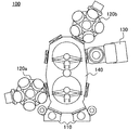
- FIG. 2 is a schematic configuration diagram of the TMR element manufacturing apparatus 100 according to the present embodiment.
- the manufacturing apparatus 100 is a cluster type manufacturing apparatus.
- the manufacturing apparatus 100 includes at least one film forming chamber and at least one chamber capable of performing oxidation, heating, and film forming (hereinafter referred to as a heating oxidation chamber). .
- the manufacturing apparatus 100 includes a load lock chamber 110, a first film forming chamber 120a, a second film forming chamber 120b, a heating oxidation chamber 130, and a transfer chamber 140.
- the load lock chamber 110, the first film formation chamber 120 a, the second film formation chamber 120 b, and the heating oxidation chamber 130 are connected via a transfer chamber 140.
- Each chamber is provided with an evacuation device, and can be independently evacuated, so that the substrate can be processed in a consistent vacuum.
- the load lock chamber 110 is a chamber for loading the substrate 1 into the manufacturing apparatus 100 and unloading the substrate 1 from the manufacturing apparatus 100.
- the first film formation chamber 120 a is a chamber for forming a film from the base layer 2 to the fixed magnetic layer 4 on the substrate 1.
- the heating oxidation chamber 130 is a chamber for depositing the tunnel barrier layer 5 by performing heat treatment, oxygen exposure treatment, film formation treatment and decompression treatment described later on the substrate 1 on which the fixed magnetic layer 4 is formed.
- the second film forming chamber 120b is a chamber for forming a film from the magnetization free layer 6 to the protective layer 7 on the substrate 1 on which the tunnel barrier layer 5 is formed.
- the manufacturing apparatus 100 may include an arbitrary apparatus such as an additional film forming chamber or a cooling chamber in addition to the above-described chambers.
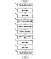
- FIG. 3 is a diagram showing a flowchart of a method for manufacturing a TMR element according to the present embodiment.
- the manufacturing apparatus 100 includes, in the first film formation chamber 120a, the base layer 2 having the first base layer 2a and the second base layer 2b as the lower magnetic electrode layer on the substrate 1, and the anti-strength.
- the pinned magnetic layer 4 having the magnetic layer 3, the ferromagnetic layer 4a, the nonmagnetic intermediate layer 4b, and the ferromagnetic layer 4c is formed (step S1).
- the fixed magnetic layer 4 is formed on the substrate 1 in step S1, but the substrate 1 on which the fixed magnetic layer 4 is formed in advance may be used. That is, in this embodiment, any method may be adopted as long as a substrate having a ferromagnetic layer on which the tunnel barrier layer 5 is formed can be prepared.
- the manufacturing apparatus 100 uses the transfer chamber 140 to transport the substrate 1 on which the fixed magnetic layer 4 is formed to the heating oxidation chamber 130 where heating has been started in advance (step S2). And the manufacturing apparatus 100 heat-processes with respect to the board
- the temperature of the substrate 1 is kept constant until the substrate 1 is transferred out of the heating oxidation chamber 130.
- the heating oxidation chamber 130 performs heating so that the substrate 1 reaches a predetermined temperature (preferably 150 to 400 ° C.). In actual temperature rise of the substrate 1, the temperature rise time may have a certain range (that is, a time difference until the substrate 1 reaches a predetermined temperature).
- any method such as a method using heat radiation using a heating resistor or a lamp heater, a method using heat conduction by placing the substrate 1 directly on a heated stage, etc. The method may be used.
- the manufacturing apparatus 100 performs an oxygen exposure process in which the surface of the substrate 1 being heated is exposed to oxygen in the heating oxidation chamber 130 (step S4).
- the oxygen exposure treatment is performed with oxygen gas or a mixed gas of oxygen gas and inert gas.
- the inert gas for example, a gas containing at least one of helium (He), neon (Ne), argon (Ar), krypton (Kr), and xenon (Xe) may be used.
- oxidation is performed after the substrate is heated, but a process of performing oxidation during heating may be used.
- a gas containing oxygen is introduced into the heating oxidation chamber 130 during heating, and the pressure in the heating oxidation chamber 130 is set to 1 ⁇ 10 ⁇ 5 Pa or more and 1 ⁇ for 10 seconds or more and 120 seconds or less. It is carried out by maintaining the pressure at 10 ⁇ 3 Pa or lower.
- the oxygen exposure treatment oxidizes at least a part of the surface of the pinned magnetic layer 4, but the first metal layer 5a ′ formed in the next step S5 has a higher oxygen affinity than the pinned magnetic layer 4.
- oxygen adhering to the surface of the pinned magnetic layer 4 is absorbed by the first metal layer 5a ′.
- a decrease in pressure during the oxygen exposure treatment or a decrease in the oxygen exposure time deteriorates the homogeneity of the first metal layer 5a ′.
- an increase in pressure during the oxygen exposure process or an increase in the oxygen exposure time causes excessive oxidation of the pinned magnetic layer 4, increasing RA (element resistance ⁇ element area) and decreasing the MR ratio. Therefore, in order to achieve good film homogeneity and MR ratio, the pressure of the oxygen exposure treatment is set to 1 ⁇ 10 ⁇ 5 Pa to 1 ⁇ 10 ⁇ 3 Pa and the oxygen exposure treatment time is set to 10 seconds to 120 seconds. The following is desirable.
- the manufacturing apparatus 100 forms the first metal layer 5a 'on the substrate 1 exposed to oxygen in the heating oxidation chamber 130 during heating (step S5).
- step S5 By performing the film formation process while heating the substrate 1, film growth is promoted, and homogenization of the film can be expected.
- the manufacturing apparatus 100 oxidizes the substrate 1 on which the first metal layer 5a ′ is formed in the heating oxidation chamber 130 during heating (step S6).
- the oxidation treatment is performed with oxygen gas or a mixed gas of oxygen gas and inert gas.
- the inert gas for example, a gas containing at least one of He, Ne, Ar, Kr, and Xe may be used.
- an inert gas such as Ar is added to keep the pressure in the heating oxidation chamber 130 higher than the vapor pressure of the first metal layer 5a '.
- the amount of oxygen introduced may be reduced.
- any method such as sealing oxidation in which the chamber is sealed, flow oxidation while exhausting the chamber, radical oxidation using active oxygen, or plasma oxidation may be used.
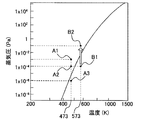
- FIG. 4 is a view showing a vapor pressure curve of Mg.
- FIG. 4 shows a point representing the pressure in each step together with a graph of the vapor pressure of Mg.
- the inside of the heating oxidation chamber 130 is set to the pressure A1
- the pressure A1 and the pressure A2 are higher than the vapor pressure of Mg. Therefore, at a temperature of 200 ° C., the Mg layer hardly evaporates during the formation and oxidation of the Mg layer.
- step S 6 when the temperature of the substrate 1 is set to 300 ° C. (573 K), when the inside of the heating oxidation chamber 130 is set to a pressure B 1 equal to the pressure A 2 at 200 ° C. during the oxidation process of the Mg layer (step S 6), the pressure B1 is smaller than the vapor pressure of Mg. For this reason, the Mg layer is vaporized before the Mg layer is sufficiently oxidized in step S6.
- An inert gas is introduced into the heated oxidation chamber 130.
- Mg is used as the first metal layer 5a ′
- the pressure in the heating oxidation chamber 130 during the oxidation treatment is 1 ⁇ 10 ⁇ 5 Pa or more and 1 ⁇ 10 ⁇ 3 Pa or less
- the temperature of the substrate 1 Is 300 ° C. (573 K)
- the pressure in the heating oxidation chamber 130 becomes a pressure B1 that is equal to or lower than the vapor pressure of Mg.
- Mg is vaporized from the first metal layer 5a ′.
- both the inert gas and the oxygen gas are added into the heating oxidation chamber 130 so that the pressure in the heating oxidation chamber 130 becomes a pressure B2 higher than the vapor pressure of Mg.
- an inert gas may be introduced in the film formation process in step S5 so that the pressure in the heating oxidation chamber 130 is higher than the vapor pressure of Mg.
- Step S7 solid unoxidized Mg that is not bonded to oxygen is vaporized by setting the pressure in the heating oxidation chamber 130 to a predetermined pressure equal to or lower than the vapor pressure of Mg.
- the predetermined pressure in the heating oxidation chamber 130 is higher than the vapor pressure of MgO, MgO is hardly vaporized. For this reason, unoxidized Mg is removed from the first metal layer 5a ', leaving only MgO, thereby forming the first metal oxide layer 5a.
- the steps S5 to S7 are repeated by one set, and the second metal layer 5b ′ is formed and then oxidized to oxidize the second metal. Oxide layer 5b is formed.
- steps S5 to S7 are repeated a plurality of times as a set, and a plurality of metal oxide layers (here, the first metal oxide layer 5a and the second metal oxide layer are used).
- a tunnel barrier layer 5 including 5b) is formed.
- steps S5 to S7 are performed only once to form the tunnel barrier layer 5 including only the first metal oxide layer 5a. That is, the present invention can also be applied to a TMR element that does not include the second metal oxide layer 5b. In that case, the tunnel barrier layer 5 has only the first metal oxide layer 5a.
- at least one of the first metal layer 5 a ′ and the second metal layer 5 b ′ that is the source of the tunnel barrier layer 5 is simply referred to as a metal layer.
- the first and second metal layers 5a ′ and 5b ′ are formed according to the set temperature based on the temperature dependence of the vapor pressure as shown in FIG. It is possible to obtain a pressure at which the metal layers 5a ′ and 5b ′ are vaporized and at which the first and second metal oxide layers 5a and 5b are not vaporized.
- the pressure reduction processing in step S7 may be performed using the pressure acquired in this way.
- the tunnel barrier layer 5 having the first metal oxide layer 5a and the second metal oxide layer 5b is formed in the same heating oxidation chamber 130. Since four types of processes of heat treatment, oxidation treatment, film formation treatment, and decompression treatment are performed in the same chamber, there is no substrate transport time for treating each process. That is, it is possible to greatly improve the throughput.
- the manufacturing apparatus 100 uses the transfer chamber 140 to move the substrate 1 subjected to the decompression process in Step S7 to the cooling chamber (Step S8).
- the cooling chamber cools the substrate 1 to 150 ° C. or lower.
- the substrate 1 may be cooled in a chamber in which film formation is performed (the first film formation chamber 120a, the second film formation chamber 120b, or the heating and oxidation chamber 130).
- the manufacturing apparatus 100 uses the transfer chamber 140 to move the substrate 1 cooled in step S9 to the second film forming chamber 120b. Then, the manufacturing apparatus 100 forms the magnetization free layer 6 and the protective layer 7 as the upper magnetic electrode layer on the substrate 1 cooled in Step S9 in the second film formation chamber 120b (Step S10). ).
- the pressure (transfer pressure) in the transfer chamber 140 is heated. It may be the same as the predetermined pressure in the oxidation chamber 130 (pressure at the end of step S7). That is, by setting the pressure in the transfer chamber 140 to a predetermined pressure, the gate valve between the heating oxidation chamber 130 and the transfer chamber 140 can be opened immediately after the end of step S7, and the transfer time can be shortened.
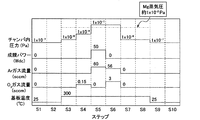
- FIG. 5 is a diagram illustrating a process time chart according to the present embodiment.
- the process time chart of FIG. 5 shows changes in each step of FIG. 3 for each item of pressure in the heating oxidation chamber 130, film formation power, Ar gas flow rate, oxygen gas flow rate, and substrate 1 temperature.
- the numbers attached to the process time chart in FIG. 5 indicate the values of the respective items. Since the process time chart of FIG. 5 schematically shows changes of each item, it changes discontinuously between steps, but actually each item changes continuously (for example, gradually increasing or decreasing). Good.
- the tunnel barrier layer 5 has only the first metal oxide layer 5a, and Mg is used as the first metal layer 5a 'that is the basis of the first metal oxide layer 5a. That is, the second metal oxide layer 5b is not formed.
- the heating temperature of the substrate 1 by the heating oxidation chamber 130 was set to 300 ° C. (573 K).
- the substrate 1 was transferred to the heating oxidation chamber 130 and subjected to heat treatment.
- the heating resistor was heated and the substrate 1 was heated by radiation.
- the temperature of the substrate 1 is about 300 ° C.
- the oxygen gas flow rate was set to 0.15 sccm
- the pressure in the heating oxidation chamber 130 was set to 1 ⁇ 10 ⁇ 4 Pa
- the oxygen exposure treatment was performed for 20 seconds. .
- the pressure in the heating oxidation chamber 130 is set to 1 ⁇ 10 ⁇ 1 Pa, which is larger than the Mg vapor pressure at 300 ° C. (1 ⁇ 10 ⁇ 2 Pa) (dashed line in FIG. 5).
- the first metal layer 5a ′ was deposited.
- the pressure in the heating oxidation chamber 130 becomes equal to or lower than the vapor pressure of Mg, and Mg is vaporized during the oxidation process. That is, in the first metal layer 5a 'during the oxidation treatment, the solid Mg is directly changed to gaseous Mg. In order to prevent this, Ar gas which is an inert gas was added to oxygen gas, and oxidation treatment was performed for 500 seconds. Thereby, the pressure in the heating oxidation chamber 130 can be made larger than the vapor pressure of Mg, and vaporization of Mg during the oxidation process can be suppressed.
- the pressure in the heating oxidation chamber 130 was set to a predetermined pressure that was equal to or lower than the vapor pressure of Mg and greater than the vapor pressure of MgO. At this time, unoxidized Mg not bonded to oxygen is vaporized, and only MgO remains on the substrate 1.
- the substrate 1 was transferred to a cooling chamber, and the substrate was cooled. After the substrate 1 was cooled to 150 ° C. or lower, the magnetization free layer 6 was formed on the substrate 1.
- FIG. 6 is a graph showing MR ratio graphs of the TMR elements according to the present example and the comparative example.
- the RA and MR ratio of the TMR element manufactured using the process of Example 1 was measured.
- the RA and MR ratio of a TMR element manufactured without performing the process of vaporizing Mg during the formation of the tunnel barrier layer 5 in the process of Example 1 were measured.
- the graph C of Example 1 is indicated by a solid line
- the graph D of the comparative example is indicated by a one-dot chain line.
- FIG. 6 shows that the TMR element manufactured using the process of Example 1 has a lower RA and a higher MR ratio than the TMR element of the comparative example.
- FIG. 7 is a diagram illustrating a process time chart according to the present embodiment.
- the tunnel barrier layer 5 has only the first metal oxide layer 5a, and Mg is used as the first metal layer 5a ′ that is the basis of the first metal oxide layer 5a. That is, the second metal oxide layer 5b is not formed.
- the heating temperature of the substrate 1 by the heating oxidation chamber 130 was set to 200 ° C. (473 K).
- the substrate 1 was transferred to the heating oxidation chamber 130 and subjected to heat treatment.
- the heating resistor was heated and the substrate 1 was heated by radiation.
- the temperature of the substrate 1 is about 200 ° C.
- the oxygen gas flow rate was set to 0.15 sccm
- the pressure in the heating oxidation chamber 130 was set to 1 ⁇ 10 ⁇ 4 Pa, and oxygen exposure treatment was performed for 20 seconds. .
- the pressure in the heating oxidation chamber 130 is set to 1 ⁇ 10 ⁇ 1 Pa, which is larger than the Mg vapor pressure at 200 ° C. (1 ⁇ 10 ⁇ 5 Pa) (dashed line in FIG. 7).
- the first metal layer 5a ′ was deposited.
- Example 2 unlike Example 1, only the oxygen gas was introduced into the heating oxidation chamber 130 to carry out the oxidation treatment.
- the Mg vapor pressure is lower when the temperature of the substrate 1 is 200 ° C. than when it is 300 ° C., it is not necessary to adjust the pressure in the heating oxidation chamber 130 by adding Ar gas.
- a decompression treatment was performed, and the pressure in the heating oxidation chamber 130 was set to a predetermined pressure that was equal to or lower than the vapor pressure of Mg and greater than the vapor pressure of MgO. At this time, unoxidized Mg not bonded to oxygen is vaporized, and only MgO remains on the substrate 1.
- the substrate 1 was transferred to the cooling chamber, and the substrate 1 was cooled. After the substrate 1 was cooled to 150 ° C. or lower, the magnetization free layer 6 was formed on the substrate 1. Also in this embodiment, a TMR element having a low RA and a high MR ratio comparable to those in Example 1 was obtained.
- FIG. 8 is a diagram illustrating a process time chart according to the present embodiment.
- the tunnel barrier layer 5 includes a first metal oxide layer 5a and a second metal oxide layer 5b, and the first metal oxide layers 5a and 5b serving as the bases of the first and second metal oxide layers 5a and 5b.
- Mg is used as the first and second metal layers 5a ′ and 5b ′.
- the heating temperature of the substrate 1 by the heating oxidation chamber 130 was set to 200 ° C. (473 K).
- the substrate 1 was transferred to the heating oxidation chamber 130 and subjected to heat treatment.
- the heating resistor was heated and the substrate 1 was heated by radiation.
- the temperature of the substrate 1 is about 200 ° C.
- the oxygen gas flow rate was set to 0.15 sccm
- the pressure in the heating oxidation chamber 130 was set to 1 ⁇ 10 ⁇ 4 Pa, and oxygen exposure treatment was performed for 20 seconds. .
- the pressure in the heating oxidation chamber 130 is set to 1 ⁇ 10 ⁇ 1 Pa, which is larger than the Mg vapor pressure at 200 ° C. (1 ⁇ 10 ⁇ 5 Pa) (the chain line in FIG. 8).
- the first metal layer 5a ′ was deposited.
- Example 2 unlike Example 1, only the oxygen gas was introduced into the heating oxidation chamber 130 to carry out the oxidation treatment.
- the Mg vapor pressure is lower when the temperature of the substrate 1 is 200 ° C. than when it is 300 ° C., it is not necessary to adjust the pressure in the heating oxidation chamber 130 by adding Ar gas.
- a decompression treatment was performed, and the pressure in the heating oxidation chamber 130 was set to a predetermined pressure that was equal to or lower than the vapor pressure of Mg and greater than the vapor pressure of MgO. At this time, unoxidized Mg not bonded to oxygen is vaporized, and only MgO remains on the substrate 1.
- the second metal layer 5b ' was formed on the first metal oxide layer 5a in which the unoxidized Mg was vaporized and became only MgO.
- the same oxidation treatment as that of the first metal layer 5a' was performed.
- a decompression treatment was performed, and the pressure in the heating oxidation chamber 130 was set to a predetermined pressure that was equal to or lower than the vapor pressure of Mg and greater than the vapor pressure of MgO. At this time, unoxidized Mg not bonded to oxygen is vaporized, and only MgO remains on the substrate 1.
- the substrate 1 was transferred to the cooling chamber, and the substrate 1 was cooled.
- the magnetization free layer 6 was formed on the substrate 1.
- the present embodiment in which the tunnel barrier layer 5 has a two-layer structure of a first metal oxide layer 5a and a second metal oxide layer 5b is compared with the first and second embodiments in which the tunnel barrier layer 5 has a one-layer structure.
- a TMR element having a high RA and a high MR ratio was obtained.
- the positions of the magnetization free layer 6 and the fixed magnetization layer 4 are limited, but the positions of the magnetization free layer 6 and the fixed magnetization layer 4 are not particularly limited in the present invention. That is, the magnetization free layer 6 may be formed below the tunnel barrier layer 5 (side closer to the substrate 1), and the fixed magnetization layer 4 may be formed above the tunnel barrier layer 5 (side far from the substrate 1).
Landscapes
- Physics & Mathematics (AREA)
- Engineering & Computer Science (AREA)
- Manufacturing & Machinery (AREA)
- Condensed Matter Physics & Semiconductors (AREA)
- General Physics & Mathematics (AREA)
- Hall/Mr Elements (AREA)
- Mram Or Spin Memory Techniques (AREA)
- Formation Of Insulating Films (AREA)
Abstract
Description
図1は、本実施形態に係るTMR素子10の概略的な断面図である。図1はTMR素子10の断面を模式的に表しており、図1に示される各層の厚さや幅は実際の構成とは異なる。図1に示すTMR素子10の構成は一例であり、TMR素子10の機能を実現できる限り、任意の層の追加や変更等が行われてよい。
図5は、本実施例に係るプロセスタイムチャートを示す図である。図5のプロセスタイムチャートは、加熱酸化チャンバ130内の圧力、成膜パワー、Arガス流量、酸素ガス流量および基板1の温度の各項目について、図3の各ステップにおける変化を示す。図5のプロセスタイムチャートに付されている数字は、各項目の値を示す。図5のプロセスタイムチャートは各項目の変化を模式的に表しているため、ステップ間で不連続に変化しているが、実際には各項目は連続的に変化(例えば漸増又は漸減)してよい。
図7は、本実施例に係るプロセスタイムチャートを示す図である。図7のプロセスタイムチャートの示す内容は、図5と同様である。本実施例において、トンネルバリア層5は第1の金属酸化物層5aのみを有し、第1の金属酸化物層5aの元となる第1の金属層5a’としてMgを使用する。すなわち、第2の金属酸化物層5bを成膜しない。加熱酸化チャンバ130による基板1の加熱温度を200℃(473K)とした。
図8は、本実施例に係るプロセスタイムチャートを示す図である。図8のプロセスタイムチャートの示す内容は、図5と同様である。本実施例において、トンネルバリア層5は第1の金属酸化物層5aと第2の金属酸化物層5bとを有し、第1および第2の金属酸化物層5a、5bの元となる第1および第2の金属層5a’、5b’としてMgを使用する。加熱酸化チャンバ130による基板1の加熱温度を200℃(473K)とした。
Claims (4)
- 第1の強磁性層が形成された基板を用意する工程と、
第1のチャンバ内において前記第1の強磁性層上にトンネルバリア層を形成する工程と、
前記トンネルバリア層上に第2の強磁性層を形成する工程と、
を含み、
前記トンネルバリア層を形成する工程は、
前記第1の強磁性層上に金属層を成膜する工程と、
前記金属層を酸化する工程と、
前記第2の強磁性層を形成する工程よりも前に、前記第1のチャンバ内を、所定温度に保ったまま前記金属層が気化する所定圧力に減圧する工程と、
を有することを特徴とする磁気抵抗素子の製造方法。 - 前記金属層を成膜する工程および前記金属層を酸化する工程は、前記所定温度で行われることを特徴とする請求項1に記載の磁気抵抗素子の製造方法。
- 前記第2の強磁性層を形成する工程は、前記第1のチャンバとは異なる第2のチャンバ内において行われ、
前記トンネルバリア層を形成する工程の後であって前記第2の強磁性層を形成する工程の前に、前記基板は前記第1のチャンバから前記第2のチャンバにトランスファーチャンバを介して搬送され、
前記所定圧力は、前記トランスファーチャンバ内の圧力と同じであることを特徴とする請求項1又は2に記載の磁気抵抗素子の製造方法。 - 前記金属層は第1および第2の金属層からなり、
前記第1および第2の金属層のうち少なくとも一方は、マグネシウムを含むことを特徴とする請求項1乃至3のいずれか1項に記載の磁気抵抗素子の製造方法。
Priority Applications (5)
| Application Number | Priority Date | Filing Date | Title |
|---|---|---|---|
| PCT/JP2015/005307 WO2017068611A1 (ja) | 2015-10-21 | 2015-10-21 | 磁気抵抗素子の製造方法 |
| JP2016514780A JP6084335B1 (ja) | 2015-10-21 | 2015-10-21 | 磁気抵抗素子の製造方法 |
| GB1611591.7A GB2548644B (en) | 2015-10-21 | 2015-10-21 | Method for manufacturing magnetoresistive device |
| US15/196,992 US9502644B1 (en) | 2015-10-21 | 2016-06-29 | Method for manufacturing magnetoresistive device |
| TW105129145A TWI613846B (zh) | 2015-10-21 | 2016-09-08 | 磁阻元件的製造方法 |
Applications Claiming Priority (1)
| Application Number | Priority Date | Filing Date | Title |
|---|---|---|---|
| PCT/JP2015/005307 WO2017068611A1 (ja) | 2015-10-21 | 2015-10-21 | 磁気抵抗素子の製造方法 |
Related Child Applications (1)
| Application Number | Title | Priority Date | Filing Date |
|---|---|---|---|
| US15/196,992 Continuation US9502644B1 (en) | 2015-10-21 | 2016-06-29 | Method for manufacturing magnetoresistive device |
Publications (1)
| Publication Number | Publication Date |
|---|---|
| WO2017068611A1 true WO2017068611A1 (ja) | 2017-04-27 |
Family
ID=56891074
Family Applications (1)
| Application Number | Title | Priority Date | Filing Date |
|---|---|---|---|
| PCT/JP2015/005307 Ceased WO2017068611A1 (ja) | 2015-10-21 | 2015-10-21 | 磁気抵抗素子の製造方法 |
Country Status (5)
| Country | Link |
|---|---|
| US (1) | US9502644B1 (ja) |
| JP (1) | JP6084335B1 (ja) |
| GB (1) | GB2548644B (ja) |
| TW (1) | TWI613846B (ja) |
| WO (1) | WO2017068611A1 (ja) |
Cited By (1)
| Publication number | Priority date | Publication date | Assignee | Title |
|---|---|---|---|---|
| JP2018129423A (ja) * | 2017-02-09 | 2018-08-16 | Tdk株式会社 | 強磁性トンネル接合体の製造方法及び強磁性トンネル接合体 |
Families Citing this family (5)
| Publication number | Priority date | Publication date | Assignee | Title |
|---|---|---|---|---|
| EP4016652A3 (en) * | 2015-03-31 | 2023-05-10 | TDK Corporation | Magnetoresistive effect element |
| GB2561790B (en) | 2016-02-01 | 2021-05-12 | Canon Anelva Corp | Manufacturing method of magneto-resistive effect device |
| JP2019057636A (ja) * | 2017-09-21 | 2019-04-11 | 東芝メモリ株式会社 | 磁気記憶装置 |
| US11004899B2 (en) * | 2019-04-26 | 2021-05-11 | Everspin Technologies, Inc. | Magnetoresistive devices and methods therefor |
| CN112750946B (zh) * | 2019-10-31 | 2023-06-02 | 上海磁宇信息科技有限公司 | 一种磁性随机存储器势垒层和自由层结构单元及其制备方法 |
Citations (4)
| Publication number | Priority date | Publication date | Assignee | Title |
|---|---|---|---|---|
| JP2011054873A (ja) * | 2009-09-04 | 2011-03-17 | Sony Corp | 不揮発性メモリ素子の製造方法 |
| WO2011081203A1 (ja) * | 2009-12-28 | 2011-07-07 | キヤノンアネルバ株式会社 | 磁気抵抗素子の製造方法 |
| JP2012114442A (ja) * | 2010-11-22 | 2012-06-14 | Headway Technologies Inc | トンネルバリアの形成方法および磁気トンネル接合(mtj)の形成方法 |
| WO2014097510A1 (ja) * | 2012-12-20 | 2014-06-26 | キヤノンアネルバ株式会社 | 磁気抵抗効果素子の製造方法 |
Family Cites Families (11)
| Publication number | Priority date | Publication date | Assignee | Title |
|---|---|---|---|---|
| US7780820B2 (en) | 2005-11-16 | 2010-08-24 | Headway Technologies, Inc. | Low resistance tunneling magnetoresistive sensor with natural oxidized double MgO barrier |
| US7479394B2 (en) | 2005-12-22 | 2009-01-20 | Magic Technologies, Inc. | MgO/NiFe MTJ for high performance MRAM application |
| JP2007305768A (ja) | 2006-05-11 | 2007-11-22 | Tdk Corp | トンネル磁気抵抗効果素子の製造方法、薄膜磁気ヘッドの製造方法及び磁気メモリの製造方法 |
| KR20100007884A (ko) | 2007-06-19 | 2010-01-22 | 캐논 아네르바 가부시키가이샤 | 터널 자기 저항 박막 및 자성 다층막 제작 장치 |
| WO2009040939A1 (ja) | 2007-09-28 | 2009-04-02 | Canon Anelva Corporation | 磁気抵抗効果を用いた負性抵抗素子 |
| WO2009157064A1 (ja) | 2008-06-25 | 2009-12-30 | キヤノンアネルバ株式会社 | トンネル磁気抵抗素子の製造方法および製造装置 |
| US20130134032A1 (en) | 2008-06-25 | 2013-05-30 | Canon Anelva Corporation | Method of fabricating and apparatus of fabricating tunnel magnetic resistive element |
| WO2010029702A1 (ja) | 2008-09-09 | 2010-03-18 | キヤノンアネルバ株式会社 | 磁気抵抗素子の製造方法、該製造方法に用いる記憶媒体 |
| JP2010080806A (ja) | 2008-09-29 | 2010-04-08 | Canon Anelva Corp | 磁気抵抗素子の製造法及びその記憶媒体 |
| JP2010109319A (ja) | 2008-09-30 | 2010-05-13 | Canon Anelva Corp | 磁気抵抗素子の製造法および記憶媒体 |
| US8609262B2 (en) * | 2009-07-17 | 2013-12-17 | Magic Technologies, Inc. | Structure and method to fabricate high performance MTJ devices for spin-transfer torque (STT)-RAM application |
-
2015
- 2015-10-21 GB GB1611591.7A patent/GB2548644B/en active Active
- 2015-10-21 JP JP2016514780A patent/JP6084335B1/ja active Active
- 2015-10-21 WO PCT/JP2015/005307 patent/WO2017068611A1/ja not_active Ceased
-
2016
- 2016-06-29 US US15/196,992 patent/US9502644B1/en active Active
- 2016-09-08 TW TW105129145A patent/TWI613846B/zh active
Patent Citations (4)
| Publication number | Priority date | Publication date | Assignee | Title |
|---|---|---|---|---|
| JP2011054873A (ja) * | 2009-09-04 | 2011-03-17 | Sony Corp | 不揮発性メモリ素子の製造方法 |
| WO2011081203A1 (ja) * | 2009-12-28 | 2011-07-07 | キヤノンアネルバ株式会社 | 磁気抵抗素子の製造方法 |
| JP2012114442A (ja) * | 2010-11-22 | 2012-06-14 | Headway Technologies Inc | トンネルバリアの形成方法および磁気トンネル接合(mtj)の形成方法 |
| WO2014097510A1 (ja) * | 2012-12-20 | 2014-06-26 | キヤノンアネルバ株式会社 | 磁気抵抗効果素子の製造方法 |
Cited By (1)
| Publication number | Priority date | Publication date | Assignee | Title |
|---|---|---|---|---|
| JP2018129423A (ja) * | 2017-02-09 | 2018-08-16 | Tdk株式会社 | 強磁性トンネル接合体の製造方法及び強磁性トンネル接合体 |
Also Published As
| Publication number | Publication date |
|---|---|
| GB2548644B (en) | 2020-09-02 |
| TWI613846B (zh) | 2018-02-01 |
| JPWO2017068611A1 (ja) | 2017-10-19 |
| GB2548644A (en) | 2017-09-27 |
| GB201611591D0 (en) | 2016-08-17 |
| TW201725766A (zh) | 2017-07-16 |
| JP6084335B1 (ja) | 2017-02-22 |
| US9502644B1 (en) | 2016-11-22 |
Similar Documents
| Publication | Publication Date | Title |
|---|---|---|
| TWI440236B (zh) | Method for manufacturing magnetoresistive elements | |
| JP6084335B1 (ja) | 磁気抵抗素子の製造方法 | |
| JP4908556B2 (ja) | 磁気抵抗素子の製造方法 | |
| JP5341082B2 (ja) | トンネル磁気抵抗素子の製造方法および製造装置 | |
| EP2421063B1 (en) | Ferromagnetic tunnel junction structure, and magnetoresistive effect element and spintronics device each comprising same | |
| US8557407B2 (en) | Low resistance tunneling magnetoresistive sensor with natural oxidized double MgO barrier | |
| TWI552399B (zh) | Method for manufacturing magnetoresistance effect elements | |
| JP5999543B2 (ja) | トンネル磁気抵抗素子の製造方法 | |
| US8431418B2 (en) | Method of manufacturing magnetic tunnel junction device and apparatus for manufacturing the same | |
| WO2007105472A1 (ja) | 磁気抵抗効果素子の製造方法及び製造装置 | |
| JP5689932B2 (ja) | トンネル磁気抵抗素子の製造方法 | |
| JP2012222093A (ja) | 磁気抵抗素子の製造方法及び製造装置 | |
| WO2010044134A1 (ja) | 磁気抵抗効果素子の製造方法及び磁気抵抗効果素子製造プログラム | |
| Lohvynov et al. | Thermostability of Spin-valve Type Functional Elements Based on Co, Cu and Ru |
Legal Events
| Date | Code | Title | Description |
|---|---|---|---|
| ENP | Entry into the national phase |
Ref document number: 2016514780 Country of ref document: JP Kind code of ref document: A |
|
| ENP | Entry into the national phase |
Ref document number: 201611591 Country of ref document: GB Kind code of ref document: A Free format text: PCT FILING DATE = 20151021 |
|
| WWE | Wipo information: entry into national phase |
Ref document number: 1611591.7 Country of ref document: GB |
|
| 121 | Ep: the epo has been informed by wipo that ep was designated in this application |
Ref document number: 15906619 Country of ref document: EP Kind code of ref document: A1 |
|
| NENP | Non-entry into the national phase |
Ref country code: DE |
|
| 122 | Ep: pct application non-entry in european phase |
Ref document number: 15906619 Country of ref document: EP Kind code of ref document: A1 |