WO2017026144A1 - Imaging device - Google Patents
Imaging device Download PDFInfo
- Publication number
- WO2017026144A1 WO2017026144A1 PCT/JP2016/062385 JP2016062385W WO2017026144A1 WO 2017026144 A1 WO2017026144 A1 WO 2017026144A1 JP 2016062385 W JP2016062385 W JP 2016062385W WO 2017026144 A1 WO2017026144 A1 WO 2017026144A1
- Authority
- WO
- WIPO (PCT)
- Prior art keywords
- unit
- control circuit
- optical system
- correction unit
- movable frame
- Prior art date
Links
Images


Classifications
-
- G—PHYSICS
- G03—PHOTOGRAPHY; CINEMATOGRAPHY; ANALOGOUS TECHNIQUES USING WAVES OTHER THAN OPTICAL WAVES; ELECTROGRAPHY; HOLOGRAPHY
- G03B—APPARATUS OR ARRANGEMENTS FOR TAKING PHOTOGRAPHS OR FOR PROJECTING OR VIEWING THEM; APPARATUS OR ARRANGEMENTS EMPLOYING ANALOGOUS TECHNIQUES USING WAVES OTHER THAN OPTICAL WAVES; ACCESSORIES THEREFOR
- G03B5/00—Adjustment of optical system relative to image or object surface other than for focusing
- G03B5/02—Lateral adjustment of lens
-
- H—ELECTRICITY
- H04—ELECTRIC COMMUNICATION TECHNIQUE
- H04N—PICTORIAL COMMUNICATION, e.g. TELEVISION
- H04N21/00—Selective content distribution, e.g. interactive television or video on demand [VOD]
- H04N21/40—Client devices specifically adapted for the reception of or interaction with content, e.g. set-top-box [STB]; Operations thereof
- H04N21/41—Structure of client; Structure of client peripherals
- H04N21/422—Input-only peripherals, i.e. input devices connected to specially adapted client devices, e.g. global positioning system [GPS]
- H04N21/42204—User interfaces specially adapted for controlling a client device through a remote control device; Remote control devices therefor
-
- H—ELECTRICITY
- H04—ELECTRIC COMMUNICATION TECHNIQUE
- H04N—PICTORIAL COMMUNICATION, e.g. TELEVISION
- H04N23/00—Cameras or camera modules comprising electronic image sensors; Control thereof
- H04N23/50—Constructional details
- H04N23/54—Mounting of pick-up tubes, electronic image sensors, deviation or focusing coils
-
- H—ELECTRICITY
- H04—ELECTRIC COMMUNICATION TECHNIQUE
- H04N—PICTORIAL COMMUNICATION, e.g. TELEVISION
- H04N23/00—Cameras or camera modules comprising electronic image sensors; Control thereof
- H04N23/50—Constructional details
- H04N23/55—Optical parts specially adapted for electronic image sensors; Mounting thereof
-
- H—ELECTRICITY
- H04—ELECTRIC COMMUNICATION TECHNIQUE
- H04N—PICTORIAL COMMUNICATION, e.g. TELEVISION
- H04N23/00—Cameras or camera modules comprising electronic image sensors; Control thereof
- H04N23/60—Control of cameras or camera modules
-
- H—ELECTRICITY
- H04—ELECTRIC COMMUNICATION TECHNIQUE
- H04N—PICTORIAL COMMUNICATION, e.g. TELEVISION
- H04N23/00—Cameras or camera modules comprising electronic image sensors; Control thereof
- H04N23/60—Control of cameras or camera modules
- H04N23/68—Control of cameras or camera modules for stable pick-up of the scene, e.g. compensating for camera body vibrations
- H04N23/681—Motion detection
- H04N23/6812—Motion detection based on additional sensors, e.g. acceleration sensors
-
- H—ELECTRICITY
- H04—ELECTRIC COMMUNICATION TECHNIQUE
- H04N—PICTORIAL COMMUNICATION, e.g. TELEVISION
- H04N23/00—Cameras or camera modules comprising electronic image sensors; Control thereof
- H04N23/60—Control of cameras or camera modules
- H04N23/68—Control of cameras or camera modules for stable pick-up of the scene, e.g. compensating for camera body vibrations
- H04N23/682—Vibration or motion blur correction
- H04N23/684—Vibration or motion blur correction performed by controlling the image sensor readout, e.g. by controlling the integration time
-
- H—ELECTRICITY
- H04—ELECTRIC COMMUNICATION TECHNIQUE
- H04N—PICTORIAL COMMUNICATION, e.g. TELEVISION
- H04N23/00—Cameras or camera modules comprising electronic image sensors; Control thereof
- H04N23/60—Control of cameras or camera modules
- H04N23/68—Control of cameras or camera modules for stable pick-up of the scene, e.g. compensating for camera body vibrations
- H04N23/682—Vibration or motion blur correction
- H04N23/685—Vibration or motion blur correction performed by mechanical compensation
- H04N23/687—Vibration or motion blur correction performed by mechanical compensation by shifting the lens or sensor position
-
- G—PHYSICS
- G03—PHOTOGRAPHY; CINEMATOGRAPHY; ANALOGOUS TECHNIQUES USING WAVES OTHER THAN OPTICAL WAVES; ELECTROGRAPHY; HOLOGRAPHY
- G03B—APPARATUS OR ARRANGEMENTS FOR TAKING PHOTOGRAPHS OR FOR PROJECTING OR VIEWING THEM; APPARATUS OR ARRANGEMENTS EMPLOYING ANALOGOUS TECHNIQUES USING WAVES OTHER THAN OPTICAL WAVES; ACCESSORIES THEREFOR
- G03B2205/00—Adjustment of optical system relative to image or object surface other than for focusing
- G03B2205/0007—Movement of one or more optical elements for control of motion blur
- G03B2205/0015—Movement of one or more optical elements for control of motion blur by displacing one or more optical elements normal to the optical axis
-
- G—PHYSICS
- G03—PHOTOGRAPHY; CINEMATOGRAPHY; ANALOGOUS TECHNIQUES USING WAVES OTHER THAN OPTICAL WAVES; ELECTROGRAPHY; HOLOGRAPHY
- G03B—APPARATUS OR ARRANGEMENTS FOR TAKING PHOTOGRAPHS OR FOR PROJECTING OR VIEWING THEM; APPARATUS OR ARRANGEMENTS EMPLOYING ANALOGOUS TECHNIQUES USING WAVES OTHER THAN OPTICAL WAVES; ACCESSORIES THEREFOR
- G03B2205/00—Adjustment of optical system relative to image or object surface other than for focusing
- G03B2205/0007—Movement of one or more optical elements for control of motion blur
- G03B2205/0038—Movement of one or more optical elements for control of motion blur by displacing the image plane with respect to the optical axis
Definitions
- the present invention relates to an imaging apparatus including a correction unit that drives an optical lens and a correction unit that drives an imaging element.
- a camera shake correction unit that suppresses image blur that occurs in a captured image due to camera shake or the like by moving the image sensor is known.
- a camera shake correction unit that suppresses image blur that occurs in a captured image due to camera shake or the like by moving an optical lens is known.
- a camera disclosed in Japanese Patent Application Laid-Open No. 2005-128092 switches between a camera shake correction unit that uses lens movement and a camera shake correction unit that uses image sensor movement according to the conditions of the subject.
- a digital camera disclosed in Japanese Patent Application Laid-Open No. 2006-128780 uses an image stabilization unit to move an optical member (imaging optical system) or image sensor from a reference image by a predetermined amount during electronic zoom processing. Pixels are complemented between pixels of the reference image by using the shifted image that was taken later. Thereby, it is possible to achieve high resolution during the electronic zoom process.
- the present invention has been made in view of the above circumstances, and in an imaging apparatus having a correction unit that drives a part of lenses of a photographing optical system and a correction unit that drives an imaging device, high-definition such as pixel shift correction.
- An object of the present invention is to provide an imaging apparatus capable of controlling one of a lens and an image sensor to a regular fixed position with respect to the other when performing correction.
- an imaging apparatus includes a shake detection unit and a first movable unit that holds a part of lenses of a photographing optical system, and the detection of the shake detection unit. Based on the result, a shake correction unit that corrects shake by moving the first movable unit in a direction perpendicular to the optical axis, a position detection unit that detects the position of the first movable unit, and an imaging unit A pixel shift unit that has a second movable portion to hold and moves the second movable portion in a direction perpendicular to the optical axis to perform pixel shift correction; and when the pixel shift unit is driven And a control circuit for controlling the shake correction unit so that the first movable part of the shake correction unit stops at a predetermined position.
- FIG. 1 is a diagram illustrating a schematic configuration of an imaging apparatus according to an embodiment of the present invention.
- FIG. 2 is a diagram of the assembled state of the optical system correction unit.
- FIG. 3 is an exploded perspective view of the optical system correction unit.
- FIG. 4 is a diagram illustrating an example of the relationship between the stroke position of the movable frame and the output voltage of the Hall element.
- FIG. 5 is a functional block diagram showing a configuration relating to feedback control of the stroke position of the movable frame.
- FIG. 6 is a diagram showing the relationship between the amplification factor of the amplifier and the position detection resolution.
- FIG. 7 is a flowchart illustrating the operation of the imaging apparatus.
- FIG. 1 is a diagram illustrating a schematic configuration of an imaging apparatus according to an embodiment of the present invention.
- An imaging apparatus 1 illustrated in FIG. 1 includes an interchangeable lens 100 and a main body 200.
- the interchangeable lens 100 is attached to the main body 200 via a mount 202 provided on the main body 200.
- the interchangeable lens 100 and the main body 200 are connected to be able to communicate.
- the interchangeable lens 100 and the main body 200 operate in cooperation.
- the imaging device 1 is not necessarily an interchangeable lens type imaging device.
- the imaging device 1 may be a lens-integrated imaging device.
- the interchangeable lens 100 includes a photographing optical system 102, a control circuit 106, and a shake detection unit 108.
- the photographing optical system 102 includes, for example, a plurality of lenses and a diaphragm, and causes a light beam from a subject (not shown) to enter the image sensor of the image sensor correction unit 206 of the main body 200.
- the imaging optical system 102 in FIG. 1 is configured by a plurality of lenses, but the imaging optical system 102 may be configured by a single lens. Further, the photographing optical system 102 may have a focus lens or may be configured as a zoom lens. In these cases, at least a part of the lenses of the photographing optical system 102 is configured to be movable along the Z direction, which is the direction along the optical axis O.
- the photographing optical system 102 of the present embodiment includes an optical system correction unit 104.
- the optical system correction unit 104 moves a part of the lenses of the photographing optical system 102 mounted on the movable frame 1042 as the first movable unit by a VCM (voice coil motor) using a coil and a magnet.
- VCM voice coil motor
- the control circuit 106 is composed of, for example, a CPU or ASIC, and controls various operations of the interchangeable lens 100.
- the control circuit 106 includes an optical system correction control circuit 1061.
- the optical system correction control circuit 1061 controls the optical system correction unit 104.
- the shake detection unit 108 is a gyro sensor, for example, and detects a shake that has occurred in the interchangeable lens 100.
- the main body 200 includes a shutter 204, an image sensor correction unit 206, a monitor 208, an operation unit 210, a control circuit 212, and a shake detection unit 214.
- the shutter 204 is a focal plane shutter disposed on the front side (the positive side in the Z direction) of the image sensor correction unit 206, for example.
- the shutter 204 is opened, the image sensor of the image sensor correction unit 206 is exposed. Further, the shutter 204 is closed to place the image sensor of the image sensor correction unit 206 in a light-shielding state.
- the imaging element correction unit 206 has an imaging unit mounted on a movable frame 2062 as a second movable unit.
- the imaging unit has an imaging element and the like.
- the imaging device generates a captured image related to the subject by imaging a subject (not shown). Further, the image sensor correction unit 206 moves the image pickup unit mounted on the movable frame 2062 as the second movable unit by a VCM (voice coil motor) using a coil and a magnet.
- VCM voice coil motor
- the monitor 208 is, for example, a liquid crystal display, and displays an image based on a captured image generated by the image sensor of the image sensor correction unit 206.
- the monitor 208 also displays a menu screen for the user to make various settings for the imaging device 1.
- the monitor 208 may include a touch panel.
- the operation unit 210 is, for example, a release button.
- the release button is a button for the user to instruct start of shooting by the imaging apparatus 1.
- the operation unit 210 includes various operation units other than the release button.
- the control circuit 212 is configured by, for example, a CPU or an ASIC, and controls the entire operation of the imaging apparatus 1 such as a shooting operation in the imaging apparatus 1.
- the control circuit 212 includes an image sensor correction control circuit 2121.
- the image sensor correction control circuit 2121 controls the image sensor correction unit 206.
- the shake detection unit 214 is a gyro sensor, for example, and detects the shake generated in the main body 200.
- the configuration of the optical system correction unit 104 and the image sensor correction unit 206 will be further described.
- a lens is mounted on a movable frame, which will be described later
- an imaging unit is mounted on the movable frame.
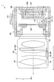
- FIG. 2 shows an assembled state of the optical system correction unit 104.
- the optical system correction unit 104 generally includes a fixed frame 1041 and a movable frame 1042. Then, the optical system correction unit 104 translates the movable frame 1042 in a plane perpendicular to the optical axis O (X direction and Y direction in FIG. 1).
- FIG. 3 is an exploded perspective view of the optical system correction unit 104.
- the optical system correction unit 104 has a fixed frame 1041, a movable frame 1042, a hole lid 1043, a yoke 1044, and a lens main substrate 1045 in detail. These are assembled in the order of the fixed frame 1041, the movable frame 1042, the hole lid 1043, the yoke 1044, and the lens main substrate 1045 as viewed from the subject side.
- the vertical and horizontal directions in the figure are defined in the direction viewed from the imaging side.
- the fixed frame 1041 has a substantially octagonal main body having a lens opening 1041a at the center, and is fixed to the main body of the interchangeable lens 100.
- An X magnet 1041b and a Y magnet 1041c are bonded to the outer periphery of the fixed frame 1041, respectively.
- the X magnet 1041b is provided on the right outer periphery (may be the left outer periphery) of the surface of the fixed frame 1041 facing the movable frame 1042 so that the Y-axis direction is long.
- the Y magnet 1041c is provided on the lower outer periphery (or the upper outer periphery) of the surface of the fixed frame 1041 facing the movable frame 1042 so that the X-axis direction is the longitudinal direction.
- the movable frame 1042 has a substantially cross-shaped main body 1042b with an opening formed in the center.
- a lens 1042 a is provided at the opening of the movable frame 1042.
- An X coil 1042c is provided at a position corresponding to the X magnet 1041b in the main body 1042b.
- a Y coil 1042d is provided at a position corresponding to the Y magnet 1041c in the main body 1042b.
- the X coil 1042c is provided so that the Y-axis direction is long so as to correspond to the X magnet 1041b.
- the Y coil 1042d is provided so that the X-axis direction is long so as to correspond to the Y magnet 1041c.
- an X Hall element 1042e serving as a position detection unit is provided at a position of the main body 1042b that is symmetrical to the position where the X coil 1042c is provided with the lens 1042a interposed therebetween.
- a Y Hall element 1042f is also provided as a position detection unit at a position of the main body 1042b symmetrical to the position where the Y coil 1042d is provided with the lens 1042a interposed therebetween.
- the X coil 1042c and Y coil 1042d, the X hall element 1032e, and the Y hall element 1042f are connected to the flexible printed circuit 1042g.
- the hole lid 1043 is an L-shaped plate member that is assembled to the main body 1042b so as to face the X Hall element 1042e and the Y Hall element 1042f.
- An X Hall magnet 1043a is provided at a position corresponding to the X Hall element 1042e on the back surface of the Hall lid 1043.
- a Y hole magnet 1043b is provided at a position corresponding to the Y Hall element 1042f on the back surface of the Hall lid 1043.
- the yoke 1044 is an L-shaped plate member made of a soft magnetic material that is assembled to the main body 1042b so as to face the X coil 1042c and the Y coil 1042d.
- the X magnet 1041b and A magnetic circuit is formed with the Y magnet 1041c.
- An X magnet may be further provided at a position corresponding to the X magnet 1041b on the back surface of the yoke 1044, and a Y magnet may be further provided at a position corresponding to the Y magnet 1041c on the back surface of the yoke 1044.
- the lens main substrate 1045 is assembled to the fixed frame 1041 so as to sandwich the movable frame 1042 between the lens main substrate 1045 and the lens main substrate 1045 is fixed to the main body of the interchangeable lens 100.
- the X magnet 1041b and Y magnet 1041c of the fixed frame 1041, and the X coil 1042c and Y coil 1042d of the movable frame 1042 are in a non-contact state.
- a control circuit 106 (not shown) is mounted on the lens main board 1045, and the control circuit 106 includes an X coil 1042c, a Y coil 1042d, and an X Hall element 1032e via a flexible printed board 1042g. And Y Hall element 1042f.
- the lens main board 1045 is provided with a flexible printed board 1045a.
- the flexible printed board 1045a is connected to the main body 200 via the mount 202.
- the movable frame 1042 when energization of either the X coil 1042c or the Y coil 1042d is started, the movable frame 1042 enters a floating state with respect to the fixed frame 1041. In this state, the movable frame 1042 is translated in a plane orthogonal to the optical axis O by controlling the magnitude of the drive current supplied to the X coil 1042c and the Y coil 1042d.
- the relative positional relationship between the X Hall element 1042e and the X Hall magnet 1043a and the relative positional relationship between the Y Hall element 1042f and the Y Hall magnet 1043b change.
- the magnitude of the magnetic field affected by the X Hall element 1042e from the X Hall magnet 1043a and the magnitude of the magnetic field affected by the Y Hall element 1042f from the Y Hall magnet 1043b change.
- the magnitude of the magnetic field received by the Hall element is proportional to the magnitude of the voltage output from the Hall element. Therefore, by associating the relationship between the stroke position of the movable frame 1042 and the output voltage of the Hall element as shown in FIG.
- the position of the movable frame 1042 is detected from the magnitude of the voltage signal output from the Hall element. Is done. It is possible to drive the movable frame 1042 to an arbitrary stroke position by controlling the magnitude of the drive current supplied to the X coil 1042c and the Y coil 1042d according to the detected stroke position of the movable frame 1042. .
- FIG. 5 is a functional block diagram showing a configuration relating to feedback control of the stroke position of the movable frame.
- the feedback control circuit in FIG. 5 is provided, for example, inside the optical system correction control circuit 1061 and the image sensor correction control circuit 2121. For example, when the movable frame 1042 is driven, feedback control by the feedback control circuit of the optical system correction control circuit 1061 is performed.
- the feedback control circuit 300 shown in FIG. 5 includes an amplifier 302, an A / D converter 304, a position calculation circuit 306, a subtractor 308, a control filter 310, and a motor driver 312.
- the feedback control circuits 300 in FIG. 5 are provided in the number corresponding to the number of VCMs. In the present embodiment, only the configuration corresponding to one VCM will be described.
- one of the VCMs (configured by a pair of X magnet and X coil or a pair of Y magnet and Y coil) is VCM 314 and one of the Hall elements (X Hall element or Y Hall element) is shown as Hall element 316.
- the amplifier 302 amplifies the analog signal (position detection signal) output from the hall element 316 according to the amplification factor set by the control circuit 106 or the control circuit 212.
- the A / D converter 304 converts the amplified position detection signal output from the amplifier 302 into a digital signal.
- the position calculation circuit 306 calculates a current position signal representing the current position of the movable frame 1042 in accordance with the digital signal converted by the A / D converter 304.
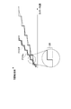
- FIG. 6 is a diagram showing the relationship between the amplification factor of the amplifier 302 and the position detection resolution.
- a thick line in FIG. 6 indicates a change in the position detection signal with respect to a change in the stroke position of the movable frame when the amplification factor is large.
- the thin line in FIG. 6 indicates a change in the position detection signal with respect to a change in the stroke position of the movable frame when the amplification factor is large.
- FIG. 6 shows the change in the position detection signal with respect to the change in the stroke position of the movable frame when the amplification factor is small.
- the position detection signal before digitization is indicated by a broken line
- the position detection signal after digitization is indicated by a solid line.
- the change in the position detection signal with respect to the change in the stroke position of the movable frame when set to a large amplification factor is the position with respect to the change in the stroke position of the movable frame when set to a small amplification factor. It becomes larger than the change of the detection signal.
- the position detection resolution is increased (the length represented by 1 LSB of the digital signal is shortened) by increasing the amplification factor. For this reason, it is effective to increase the amplification factor when highly accurate position control of the movable frame is required.
- the range of stroke positions where position detection is possible becomes narrower. Therefore, if the amplification factor is increased, it becomes difficult to control the position of the movable frame in a wide range. For this reason, when it is necessary to control the position of the movable frame in a relatively wide range, it is effective to reduce the amplification factor.
- the subtracter 308 outputs, to the control filter 310, a deviation signal between the drive target position signal indicating the drive target position of the movable frame input from the control circuit 106 or the control circuit 212 and the current position signal generated by the position calculation circuit 306, for example. Output.
- the control filter 310 has a digital filter configured by combining a plurality of IIR (Infinite Impulse Response) filters, for example, and outputs a drive current value based on the deviation signal output from the subtractor 308 to the motor driver 312. .
- the drive current value represents a current value that needs to be passed through the corresponding coil to drive the movable frame 1042 to the target position, and is generated by applying a digital filter to the deviation signal. By applying the digital filter, the drive current value becomes a desired state matched with the characteristics of the VCM 314.
- the motor driver 312 supplies current to the corresponding coil of the movable frame based on the drive current value output from the control filter 310. Based on the drive current value output from the control filter 310, the motor driver 312 drives the VCM 314 (actually the coil constituting the VCM 314) by PWM (Pulse Width Modulation).
- the drive current value is, for example, a value representing the duty of PWM drive.
- FIG. 7 is a flowchart showing the operation of the imaging apparatus 1. The process of FIG. 7 is performed by the cooperative operation of the control circuit 106 and the control circuit 212.
- step S101 the control circuit 212 determines which mode the operation mode of the image sensor correction control circuit 2121 is set to.
- the image sensor correction control circuit 2121 in this embodiment has at least a blur correction mode, a still mode, and a pixel shift mode.
- the shake correction mode of the image sensor correction control circuit 2121 controls the image sensor correction unit 206 to detect the shake of the image pickup unit mounted on the movable frame (movable frame 2062 of the image sensor correction unit 206) as the second movable unit. In this mode, image blur that occurs in a captured image due to camera shake or the like is suppressed by moving according to the output of the unit 214. That is, in the shake correction mode of the image sensor correction control circuit 2121, the image sensor correction unit 206 functions as a shake correction unit.
- the stationary mode of the image sensor correction control circuit 2121 is the second movable so that the movable frame (movable frame 2062 of the image sensor correction unit 206) as the second movable part is stationary at a predetermined regular fixed position.
- This is a mode for controlling the position of the movable frame (movable frame 2062 of the image sensor correction unit 206) as a unit.
- This regular fixed position is, for example, the optical center position. Note that “still” in the still mode of the image sensor correction control circuit 2121 means that the moving amount of the movable frame is suppressed within a range that can be regarded as having no influence on the captured image.
- the image sensor which is mounted on the movable frame (movable frame 2062 of the image sensor correction unit 206) as the second movable unit by controlling the image sensor correction unit 206 is set to one pixel.
- Pixel shift correction that obtains a high-resolution captured image by performing multiple shootings while moving with high accuracy by an amount equivalent to half the pitch of the image, and combining multiple captured images obtained by multiple shootings Is the mode in which That is, in the pixel shift mode of the image sensor correction control circuit 2121, the image sensor correction unit 206 functions as a pixel shift unit.
- the control circuit 212 determines that the operation mode is the shake correction mode. In this case, the process proceeds to step S102.
- the control circuit 212 determines to set the operation mode to the pixel shift mode. In this case, the process proceeds to step S106.
- the control circuit 212 determines that the operation mode is the still mode. In this case, the process proceeds to step S108.
- the control circuit 212 sets the image sensor correction control circuit 2121 to the shake correction mode.
- the control circuit 212 sets the amplification factor of the amplifier 302 of the image sensor correction control circuit 2121 for the shake correction mode.
- the amplification factor for the shake correction mode is a smaller amplification factor than the amplification factor for the pixel shift mode.
- the amplification factor is set small.
- the amplification factor is actually set according to the required position detection resolution. For example, when the position detection resolution required according to the shake correction mode is 0.6 ⁇ m / LSB, the amplification factor in the amplifier 302 is set so that the position detection resolution of 0.6 ⁇ m / LSB is obtained.
- step S103 the control circuit 106 determines which mode the operation mode of the optical system correction control circuit 1061 is set to.
- the optical system correction control circuit 1061 in this embodiment has at least a shake correction mode and a still mode.
- the blur correction mode of the optical system correction control circuit 1061 controls the optical system correction unit 104 to detect a lens mounted on a movable frame (movable frame 1042 of the optical system correction unit 104) as a first movable unit. In this mode, image blurring that occurs in a captured image due to camera shake or the like is suppressed by moving according to the output of 108. That is, in the shake correction mode of the optical system correction control circuit 1061, the optical system correction unit 104 functions as a shake correction unit.
- the stationary mode of the optical system correction control circuit 1061 is such that the movable frame (movable frame 1042 of the optical system correction unit 104) as the first movable unit is stationary at a predetermined regular fixed position. In this mode, the position of the movable frame (movable frame 1042 of the optical system correction unit 104) as a unit is controlled with high accuracy.
- This regular fixed position is, for example, the optical center position.
- stillness in the still mode of the optical system correction control circuit 1061 also means that the amount of movement of the movable frame is suppressed within a range that can be regarded as not affecting the captured image.
- the optical system correction control circuit 1061 is set to the still mode.
- highly accurate position control of the movable frame is required.
- the movable frame (the movable frame 2062 of the image sensor correction unit 206) as the second movable unit with high accuracy
- the movable frame (the movable frame 1042 of the optical system correction unit 104) as the first movable unit. ) Needs to be stationary with high accuracy with respect to the movable frame (movable frame 2062 of the image sensor correction unit 206) as the second movable portion.
- the stationary control of the movable frame is performed with higher accuracy in the stationary mode of the optical system correction control circuit 1061 than in the stationary mode of the image sensor correction control circuit 2121.
- control circuit 212 controls to set the operation mode of the optical system correction control circuit 1061 to the shake correction mode. Instruct the circuit 106. In response to this instruction, the control circuit 106 determines to set the operation mode to the shake correction mode. In this case, the process proceeds to step S104.
- the control circuit 212 instructs the control circuit 106 to set the operation mode of the optical system correction control circuit 1061 to the still mode. In response to this instruction, the control circuit 106 determines to set the operation mode to the stationary mode. In this case, the process proceeds to step S105.
- step S104 the control circuit 106 sets the optical system correction control circuit 1061 to the shake correction mode. Thereafter, the process of FIG. 7 is terminated.
- the control circuit 106 sets the amplification factor of the amplifier 302 of the optical system correction control circuit 1061 for the shake correction mode.
- the gain for the shake correction mode is smaller than that for the still mode.
- the amplification factor is set small. The amplification factor is actually set according to the required position detection resolution.
- the amplification factor in the amplifier 302 is set so that the position detection resolution of 0.6 ⁇ m / LSB is obtained.
- blur correction is performed using the optical system correction unit 104 and the image sensor correction unit 206 in combination. Since this process is well known, a description thereof will be omitted.
- the number of correction stages for blur correction is improved by cooperative control of the optical system correction unit 104 and the image sensor correction unit 206. Is possible.
- step S105 the control circuit 106 sets the optical system correction control circuit 1061 to the still mode. Thereafter, the process of FIG. 7 is terminated.
- the control circuit 106 sets the amplification factor of the amplifier 302 of the optical system correction control circuit 1061 for the still mode.
- the gain for the still mode is a larger gain than the gain for the shake correction mode. This is for highly accurate stationary control.
- the amplification factor is actually set according to the required position detection resolution. For example, when the position detection resolution required according to the pixel shift mode is 0.4 ⁇ m / LSB, the position detection resolution required in the still mode of the optical system correction control circuit 1061 is also 0.4 ⁇ m / LSB.
- the amplification factor in the amplifier 302 is set so that the position detection resolution of 0.4 ⁇ m / LSB can be obtained. After such setting, shake correction using the image sensor correction unit 206 is executed. Since this process is well known, a description thereof will be omitted.
- step S106 the control circuit 212 sets the image sensor correction control circuit 2121 to the pixel shift mode.
- the control circuit 212 sets the amplification factor of the amplifier 302 of the image sensor correction control circuit 2121 for the pixel shift mode.
- the gain for the pixel shift mode is a larger gain than the gain for the blur correction mode.
- the amplification factor is set large.
- the amplification factor is actually set according to the required position detection resolution. For example, when the position detection resolution required according to the pixel shift mode is 0.4 ⁇ m / LSB, the amplification factor in the amplifier 302 is set so that the position detection resolution of 0.4 ⁇ m / LSB is obtained.
- step S107 the control circuit 106 sets the optical system correction control circuit 1061 to the still mode. Thereafter, the process of FIG. 7 is terminated.
- the control circuit 106 sets the amplification factor of the amplifier 302 of the optical system correction control circuit 1061 for the still mode. As described above, the amplification factor for the still mode of the optical system correction control circuit 1061 is larger than the amplification factor for the shake correction mode.
- pixel-shifted shooting using the image sensor correction unit 206 is executed. Since this process is well known, a description thereof will be omitted.
- step S108 the control circuit 212 sets the image sensor correction control circuit 2121 to the still mode.
- the control circuit 212 sets the amplification factor of the amplifier 302 of the image sensor correction control circuit 2121 for the still mode.
- the still in the still mode of the image sensor correction control circuit 2121 means that the moving amount of the movable frame is suppressed within a range that can be regarded as having no influence on the captured image. Therefore, if such position control of the movable frame can be performed with the position detection resolution in the shake correction mode, the gain in the still mode may be the same as the gain in the shake correction mode.
- the gain in the still mode needs to be the same as the gain in the pixel shift mode.
- the gain in the still mode may be different from both the gain in the blur correction mode and the gain in the pixel shift mode.
- step S109 the control circuit 106 determines which mode the operation mode of the optical system correction control circuit 1061 is set to.
- the control circuit 212 instructs the control circuit 106 to set the operation mode of the optical system correction control circuit 1061 to the blur correction mode. .
- the control circuit 106 determines to set the operation mode to the shake correction mode. In this case, the process proceeds to step S110.
- the control circuit 212 instructs the control circuit 106 to set the operation mode of the optical system correction control circuit 1061 to the still mode.
- the control circuit 106 determines to set the operation mode to the stationary mode. In this case, the process proceeds to step S111.
- step S110 the control circuit 106 sets the optical system correction control circuit 1061 to the shake correction mode. Thereafter, the process of FIG. 7 is terminated.
- the control circuit 106 sets the amplification factor of the amplifier 302 of the optical system correction control circuit 1061 for the shake correction mode. After such setting, shake correction using the optical system correction unit 104 is executed. Since this process is well known, a description thereof will be omitted.
- step S111 the control circuit 106 sets the optical system correction control circuit 1061 to the still mode. Thereafter, the process of FIG. 7 is terminated.
- the control circuit 106 sets the amplification factor of the amplifier 302 of the optical system correction control circuit 1061 for the still mode.
- the movable frame 1042 of the optical system correction unit 104 and the movable frame 2062 of the image sensor correction unit 206 are both controlled to be stationary at a regular fixed position (optical center position).
- the optical system correction unit in the imaging apparatus having the optical system correction unit 104 and the image sensor correction unit 206, when the pixel shift correction by the image sensor correction unit 206 is performed, the optical system correction unit.
- the movable frame 1042 104 is controlled with high accuracy.
- the movable frame is oscillated within a minute deviation range.
- by performing position control by increasing the position detection resolution it is possible to make the movable frame stationary with the same accuracy as mechanically fixing the movable frame. Thereby, pixel shifting by the image sensor correction unit 206 is performed with high accuracy.
- the image sensor correction unit 206 is stopped by VCM feedback control in the still mode of the image sensor correction control circuit 2121.
- the image sensor correction unit 206 may be configured to be stopped by a mechanical mechanism in the still mode of the image sensor correction control circuit 2121.
- pixel shift correction is performed using the image sensor correction unit 206.
- the pixel shift correction may be configured to be performed using the optical system correction unit 104.
- the amplification factor is set so as to be a mode with high position detection resolution.
- the position detection resolution is changed by setting the amplification factor of the amplifier 302.
- the position detection resolution may be changed by increasing the drive voltage or drive current of the Hall element 316.
- the position detection resolution may be changed by both the setting of the amplification factor of the amplifier 302 and the setting of the Hall element 316.
- the amplification factor of the control filter 310 it is possible to improve the responsiveness during the stationary control and to make the movable frame stationary in a shorter time.
- the present invention has been described above based on the embodiments, but the present invention is not limited to the above-described embodiments, and various modifications and applications are naturally possible within the scope of the present invention.
- the configuration of the optical system correction unit 104 described above is an example and can be changed as appropriate.
- the VCM configuration may be different.
- a magnet for position detection is provided on the fixed frame, and a hall element is provided on the movable frame.
- a magnet for position detection may be provided on the movable frame, and a Hall element may be provided on the fixed frame.
Abstract
This imaging device (1) comprises: a shake detector (108); an optical system correction unit (104) having a movable frame (1042) that holds a portion of lenses in an imaging optical system 102 and corrects shake by moving the movable frame (1042) in a direction orthogonal to an optical axis; an imaging element correction unit (206) having a movable frame (2062) that holds an imaging unit and performs pixel shift correction by moving the movable frame (2062) in a direction orthogonal to the optical axis; and an optical system correction control circuit (1061) that controls the optical system correction unit (104) so that the movable frame (1042) stops at a predetermined position while imaging element correction unit (206) performs the pixel shift correction.
Description
本発明は、光学レンズを駆動する補正ユニットと撮像素子を駆動する補正ユニットとを備えた撮像装置に関する。
The present invention relates to an imaging apparatus including a correction unit that drives an optical lens and a correction unit that drives an imaging element.
撮像素子を移動させることで手ぶれ等に起因して撮像画像に生じる像ぶれを抑制する手ぶれ補正ユニットが知られている。また、光学レンズを移動させることで手ぶれ等に起因して撮像画像に生じる像ぶれを抑制する手ぶれ補正ユニットも知られている。近年、レンズ移動を用いた手ぶれ補正ユニットと撮像素子移動を用いた手ぶれ補正ユニットとを併用する提案がなされている。例えば、日本国特開2005-128092号公報のカメラは、被写体の条件に応じてレンズ移動を用いた手ぶれ補正ユニットと撮像素子移動を用いた手ぶれ補正ユニットとを切り換えるようにしている。
A camera shake correction unit that suppresses image blur that occurs in a captured image due to camera shake or the like by moving the image sensor is known. There is also known a camera shake correction unit that suppresses image blur that occurs in a captured image due to camera shake or the like by moving an optical lens. In recent years, proposals have been made to use both a camera shake correction unit using lens movement and a camera shake correction unit using image sensor movement. For example, a camera disclosed in Japanese Patent Application Laid-Open No. 2005-128092 switches between a camera shake correction unit that uses lens movement and a camera shake correction unit that uses image sensor movement according to the conditions of the subject.
また、近年、このような手ぶれ補正ユニットを手ぶれ補正以外に用いるようにした各種の提案がなされている。例えば、日本国特開2006-128780号公報のデジタルカメラは、電子ズーム処理の際に、手ぶれ補正ユニットを用いて光学部材(撮影光学系)又は撮像素子を基準画像から所定のずらし量だけ移動させてから撮影したずらし画像により、基準画像の画素間に画素を補完するようにしている。これにより、電子ズーム処理時の高解像度化を図ることができる。
In recent years, various proposals have been made to use such an image stabilization unit for purposes other than image stabilization. For example, a digital camera disclosed in Japanese Patent Application Laid-Open No. 2006-128780 uses an image stabilization unit to move an optical member (imaging optical system) or image sensor from a reference image by a predetermined amount during electronic zoom processing. Pixels are complemented between pixels of the reference image by using the shifted image that was taken later. Thereby, it is possible to achieve high resolution during the electronic zoom process.
一般に、日本国特開2006-128780号公報の画素ずらし補正等を行う場合には、光学レンズと撮像素子のうちの一方を固定し、他方を駆動することが望ましい。ここで、日本国特開2005-128092号公報のように光学レンズと撮像素子の両方を駆動できる場合、駆動される側に対して駆動されない側を正規の固定位置に正確に固定しておく必要がある。
Generally, when performing pixel shift correction or the like described in Japanese Patent Laid-Open No. 2006-128780, it is desirable to fix one of the optical lens and the image sensor and drive the other. Here, when both the optical lens and the image sensor can be driven as in Japanese Patent Application Laid-Open No. 2005-128092, it is necessary to accurately fix the non-driven side to the regular fixed position with respect to the driven side. There is.
本発明は、前記の事情に鑑みてなされたもので、撮影光学系の一部のレンズを駆動する補正ユニットと撮像素子を駆動する補正ユニットとを有する撮像装置において、画素ずらし補正等の高精細補正を行う際に、レンズと撮像素子の一方を他方に対して正規の固定位置に制御することが可能な撮像装置を提供することを目的とする。
The present invention has been made in view of the above circumstances, and in an imaging apparatus having a correction unit that drives a part of lenses of a photographing optical system and a correction unit that drives an imaging device, high-definition such as pixel shift correction. An object of the present invention is to provide an imaging apparatus capable of controlling one of a lens and an image sensor to a regular fixed position with respect to the other when performing correction.
前記の目的を達成するために、本発明の一態様の撮像装置は、ぶれ検出部と、撮影光学系の一部のレンズを保持する第1の可動部を有し、前記ぶれ検出部の検出結果に基づいて、前記第1の可動部を光軸と垂直な方向に移動させてぶれを補正するぶれ補正ユニットと、前記第1の可動部の位置を検出する位置検出部と、撮像部を保持する第2の可動部を有し、当該第2の可動部を前記光軸と垂直な方向に移動させて画素ずらし補正を行う画素ずらしユニットと、前記画素ずらしユニットが駆動されている際に、前記ぶれ補正ユニットの前記第1の可動部が所定の位置で停止するように前記ぶれ補正ユニットを制御する制御回路とを具備する。
In order to achieve the above object, an imaging apparatus according to one embodiment of the present invention includes a shake detection unit and a first movable unit that holds a part of lenses of a photographing optical system, and the detection of the shake detection unit. Based on the result, a shake correction unit that corrects shake by moving the first movable unit in a direction perpendicular to the optical axis, a position detection unit that detects the position of the first movable unit, and an imaging unit A pixel shift unit that has a second movable portion to hold and moves the second movable portion in a direction perpendicular to the optical axis to perform pixel shift correction; and when the pixel shift unit is driven And a control circuit for controlling the shake correction unit so that the first movable part of the shake correction unit stops at a predetermined position.
以下、図面を参照して本発明の実施形態を説明する。図1は、本発明の一実施形態に係る撮像装置の概略の構成を示す図である。図1に示す撮像装置1は、交換レンズ100と、本体200とを有している。交換レンズ100は、本体200に設けられたマウント202を介して本体200に装着される。交換レンズ100が本体200に装着されることによって、交換レンズ100と本体200とは通信自在に接続される。これにより、交換レンズ100と本体200とは協働して動作する。なお、撮像装置1は、必ずしもレンズ交換式の撮像装置でなくて良い。例えば、撮像装置1は、レンズ一体型の撮像装置であっても良い。
Hereinafter, embodiments of the present invention will be described with reference to the drawings. FIG. 1 is a diagram illustrating a schematic configuration of an imaging apparatus according to an embodiment of the present invention. An imaging apparatus 1 illustrated in FIG. 1 includes an interchangeable lens 100 and a main body 200. The interchangeable lens 100 is attached to the main body 200 via a mount 202 provided on the main body 200. When the interchangeable lens 100 is attached to the main body 200, the interchangeable lens 100 and the main body 200 are connected to be able to communicate. Thereby, the interchangeable lens 100 and the main body 200 operate in cooperation. The imaging device 1 is not necessarily an interchangeable lens type imaging device. For example, the imaging device 1 may be a lens-integrated imaging device.
交換レンズ100は、撮影光学系102と、制御回路106と、ぶれ検出部108とを有している。撮影光学系102は、例えば複数のレンズ及び絞りを含み、図示しない被写体からの光束を本体200の撮像素子補正ユニット206の撮像素子に入射させる。図1の撮影光学系102は、複数のレンズによって構成されているが、撮影光学系102は、1枚のレンズで構成されていても良い。また、撮影光学系102は、フォーカスレンズを有していても良いし、ズームレンズとして構成されていても良い。これらの場合、撮影光学系102の少なくとも一部のレンズは、光軸Oに沿った方向であるZ方向に沿って移動自在に構成されている。
The interchangeable lens 100 includes a photographing optical system 102, a control circuit 106, and a shake detection unit 108. The photographing optical system 102 includes, for example, a plurality of lenses and a diaphragm, and causes a light beam from a subject (not shown) to enter the image sensor of the image sensor correction unit 206 of the main body 200. The imaging optical system 102 in FIG. 1 is configured by a plurality of lenses, but the imaging optical system 102 may be configured by a single lens. Further, the photographing optical system 102 may have a focus lens or may be configured as a zoom lens. In these cases, at least a part of the lenses of the photographing optical system 102 is configured to be movable along the Z direction, which is the direction along the optical axis O.
また、本実施形態の撮影光学系102は、光学系補正ユニット104を内蔵している。光学系補正ユニット104は、第1の可動部としての可動枠1042に搭載された撮影光学系102の一部のレンズをコイルと磁石とを用いたVCM(ボイスコイルモータ)によって移動させる。光学系補正ユニット104の構成については後で詳しく説明する。
In addition, the photographing optical system 102 of the present embodiment includes an optical system correction unit 104. The optical system correction unit 104 moves a part of the lenses of the photographing optical system 102 mounted on the movable frame 1042 as the first movable unit by a VCM (voice coil motor) using a coil and a magnet. The configuration of the optical system correction unit 104 will be described in detail later.
制御回路106は、例えばCPUやASICで構成され、交換レンズ100の各種の動作を制御する。制御回路106は、光学系補正制御回路1061を有している。光学系補正制御回路1061は、光学系補正ユニット104の制御を行う。
The control circuit 106 is composed of, for example, a CPU or ASIC, and controls various operations of the interchangeable lens 100. The control circuit 106 includes an optical system correction control circuit 1061. The optical system correction control circuit 1061 controls the optical system correction unit 104.
ぶれ検出部108は、例えばジャイロセンサであり、交換レンズ100に発生したぶれを検出する。
The shake detection unit 108 is a gyro sensor, for example, and detects a shake that has occurred in the interchangeable lens 100.
本体200は、シャッタ204と、撮像素子補正ユニット206と、モニタ208と、操作部210と、制御回路212と、ぶれ検出部214とを有している。
The main body 200 includes a shutter 204, an image sensor correction unit 206, a monitor 208, an operation unit 210, a control circuit 212, and a shake detection unit 214.
シャッタ204は、例えば撮像素子補正ユニット206の前側(Z方向の正の側とする)に配置されるフォーカルプレーンシャッタである。このシャッタ204は、開かれることにより、撮像素子補正ユニット206の撮像素子を露出状態にする。また、シャッタ204は、閉じられることにより、撮像素子補正ユニット206の撮像素子を遮光状態にする。
The shutter 204 is a focal plane shutter disposed on the front side (the positive side in the Z direction) of the image sensor correction unit 206, for example. When the shutter 204 is opened, the image sensor of the image sensor correction unit 206 is exposed. Further, the shutter 204 is closed to place the image sensor of the image sensor correction unit 206 in a light-shielding state.
撮像素子補正ユニット206は、第2の可動部としての可動枠2062に搭載された撮像部を有している。撮像部は、撮像素子等を有している。撮像素子は、図示しない被写体を撮像することによって被写体に係る撮像画像を生成する。また、撮像素子補正ユニット206は、第2の可動部としての可動枠2062に搭載された撮像部をコイルと磁石とを用いたVCM(ボイスコイルモータ)によって移動させる。
The imaging element correction unit 206 has an imaging unit mounted on a movable frame 2062 as a second movable unit. The imaging unit has an imaging element and the like. The imaging device generates a captured image related to the subject by imaging a subject (not shown). Further, the image sensor correction unit 206 moves the image pickup unit mounted on the movable frame 2062 as the second movable unit by a VCM (voice coil motor) using a coil and a magnet.
モニタ208は、例えば液晶ディスプレイであり、撮像素子補正ユニット206の撮像素子で生成された撮像画像に基づく画像を表示する。また、モニタ208は、ユーザが撮像装置1の各種の設定を行うためのメニュー画面を表示する。なお、モニタ208は、タッチパネルを有していても良い。
The monitor 208 is, for example, a liquid crystal display, and displays an image based on a captured image generated by the image sensor of the image sensor correction unit 206. The monitor 208 also displays a menu screen for the user to make various settings for the imaging device 1. Note that the monitor 208 may include a touch panel.
操作部210は、例えばレリーズボタンである。レリーズボタンは、ユーザが撮像装置1による撮影開始を指示するためのボタンである。なお、操作部210は、レリーズボタン以外の各種の操作部も含む。
The operation unit 210 is, for example, a release button. The release button is a button for the user to instruct start of shooting by the imaging apparatus 1. The operation unit 210 includes various operation units other than the release button.
制御回路212は、例えばCPUやASICで構成され、撮像装置1における撮影動作等の撮像装置1の全体の動作を制御する。制御回路212は、撮像素子補正制御回路2121を有している。撮像素子補正制御回路2121は、撮像素子補正ユニット206の制御を行う。
The control circuit 212 is configured by, for example, a CPU or an ASIC, and controls the entire operation of the imaging apparatus 1 such as a shooting operation in the imaging apparatus 1. The control circuit 212 includes an image sensor correction control circuit 2121. The image sensor correction control circuit 2121 controls the image sensor correction unit 206.
ぶれ検出部214は、例えばジャイロセンサであり、本体200に発生したぶれを検出する。
The shake detection unit 214 is a gyro sensor, for example, and detects the shake generated in the main body 200.
次に、光学系補正ユニット104及び撮像素子補正ユニット206の構成についてさらに説明する。ここで、光学系補正ユニット104では後で説明する可動枠にレンズが搭載されているのに対し、撮像素子補正ユニット206では可動枠に撮像部が搭載されている。これ以外の構成は、光学系補正ユニット104と撮像素子補正ユニット206とで大きな相違はない。したがって、以下では、光学系補正ユニット104の構成についてのみ説明し、撮像素子補正ユニット206の構成についての説明は省略する。
Next, the configuration of the optical system correction unit 104 and the image sensor correction unit 206 will be further described. Here, in the optical system correction unit 104, a lens is mounted on a movable frame, which will be described later, whereas in the image sensor correction unit 206, an imaging unit is mounted on the movable frame. In other configurations, there is no significant difference between the optical system correction unit 104 and the image sensor correction unit 206. Therefore, only the configuration of the optical system correction unit 104 will be described below, and the description of the configuration of the image sensor correction unit 206 will be omitted.
図2は、光学系補正ユニット104の組み立て状態の図を示している。図2に示すように、光学系補正ユニット104は、概略的には、固定枠1041と、可動枠1042とを有している。そして、光学系補正ユニット104は、可動枠1042を光軸Oに対して垂直な面内(図1のX方向及びY方向)で平行移動させる。
FIG. 2 shows an assembled state of the optical system correction unit 104. As shown in FIG. 2, the optical system correction unit 104 generally includes a fixed frame 1041 and a movable frame 1042. Then, the optical system correction unit 104 translates the movable frame 1042 in a plane perpendicular to the optical axis O (X direction and Y direction in FIG. 1).
図3は、光学系補正ユニット104の分解斜視図である。図3に示すように、光学系補正ユニット104は、詳細には、固定枠1041と、可動枠1042と、ホール蓋1043と、ヨーク1044と、レンズ用メイン基板1045とを有している。これらは、被写体側がら見て、固定枠1041、可動枠1042、ホール蓋1043、ヨーク1044、レンズ用メイン基板1045の順で組みつけられている。なお、以下の説明においては、撮像側から見た方向で図の上下左右方向が定義されている。
FIG. 3 is an exploded perspective view of the optical system correction unit 104. As shown in FIG. 3, the optical system correction unit 104 has a fixed frame 1041, a movable frame 1042, a hole lid 1043, a yoke 1044, and a lens main substrate 1045 in detail. These are assembled in the order of the fixed frame 1041, the movable frame 1042, the hole lid 1043, the yoke 1044, and the lens main substrate 1045 as viewed from the subject side. In the following description, the vertical and horizontal directions in the figure are defined in the direction viewed from the imaging side.
固定枠1041は、中央部にレンズ用の開口1041aを有する略八角形状の本体を有し、交換レンズ100の本体に対して固定されている。固定枠1041の外周には、Xマグネット1041bと、Yマグネット1041cがそれぞれ接着されている。Xマグネット1041bは、固定枠1041の可動枠1042と対する側の面における右側外周(左側外周であってもよい)に、Y軸方向が長手となるように設けられている。Yマグネット1041cは、固定枠1041の可動枠1042と対する側の面の下側外周(上側外周であってもよい)に、X軸方向が長手となるように設けられている。
The fixed frame 1041 has a substantially octagonal main body having a lens opening 1041a at the center, and is fixed to the main body of the interchangeable lens 100. An X magnet 1041b and a Y magnet 1041c are bonded to the outer periphery of the fixed frame 1041, respectively. The X magnet 1041b is provided on the right outer periphery (may be the left outer periphery) of the surface of the fixed frame 1041 facing the movable frame 1042 so that the Y-axis direction is long. The Y magnet 1041c is provided on the lower outer periphery (or the upper outer periphery) of the surface of the fixed frame 1041 facing the movable frame 1042 so that the X-axis direction is the longitudinal direction.
可動枠1042は、中央部に開口が形成された略十字状の本体1042bを有している。可動枠1042の開口部にはレンズ1042aが設けられている。そして、本体1042bにおけるXマグネット1041bと対応する位置には、Xコイル1042cが設けられている。また、本体1042bにおけるYマグネット1041cと対応する位置には、Yコイル1042dが設けられている。Xコイル1042cは、Xマグネット1041bと対応するように、Y軸方向が長手となるように設けられている。Yコイル1042dは、Yマグネット1041cと対応するように、X軸方向が長手となるように設けられている。また、レンズ1042aを挟んでXコイル1042cが設けられている位置と対称な本体1042bの位置には、位置検出部としてのXホール素子1042eが設けられている。また、レンズ1042aを挟んでYコイル1042dが設けられている位置と対称な本体1042bの位置には、同じく位置検出部としてのYホール素子1042fが設けられている。Xコイル1042c及びYコイル1042dとXホール素子1032e及びYホール素子1042fとはフレキシブルプリント基板1042gに接続されている。
The movable frame 1042 has a substantially cross-shaped main body 1042b with an opening formed in the center. A lens 1042 a is provided at the opening of the movable frame 1042. An X coil 1042c is provided at a position corresponding to the X magnet 1041b in the main body 1042b. A Y coil 1042d is provided at a position corresponding to the Y magnet 1041c in the main body 1042b. The X coil 1042c is provided so that the Y-axis direction is long so as to correspond to the X magnet 1041b. The Y coil 1042d is provided so that the X-axis direction is long so as to correspond to the Y magnet 1041c. Further, an X Hall element 1042e serving as a position detection unit is provided at a position of the main body 1042b that is symmetrical to the position where the X coil 1042c is provided with the lens 1042a interposed therebetween. A Y Hall element 1042f is also provided as a position detection unit at a position of the main body 1042b symmetrical to the position where the Y coil 1042d is provided with the lens 1042a interposed therebetween. The X coil 1042c and Y coil 1042d, the X hall element 1032e, and the Y hall element 1042f are connected to the flexible printed circuit 1042g.
ホール蓋1043は、Xホール素子1042e及びYホール素子1042fと対向するように本体1042bに組みつけられるL字状の板部材である。ホール蓋1043の裏面におけるXホール素子1042eと対応する位置には、Xホールマグネット1043aが設けられている。また、ホール蓋1043の裏面におけるYホール素子1042fと対応する位置には、Yホールマグネット1043bが設けられている。
The hole lid 1043 is an L-shaped plate member that is assembled to the main body 1042b so as to face the X Hall element 1042e and the Y Hall element 1042f. An X Hall magnet 1043a is provided at a position corresponding to the X Hall element 1042e on the back surface of the Hall lid 1043. A Y hole magnet 1043b is provided at a position corresponding to the Y Hall element 1042f on the back surface of the Hall lid 1043.
ヨーク1044は、Xコイル1042c及びYコイル1042dと対向するように本体1042bに組みつけられる軟質磁性材料製のL字状の板部材であり、可動枠1042に組みつけられることにより、Xマグネット1041b及びYマグネット1041cとの間で磁気回路を形成する。なお、ヨーク1044の裏面におけるXマグネット1041bと対応する位置にXマグネットがさらに設けられ、ヨーク1044の裏面におけるYマグネット1041cと対応する位置にYマグネットがさらに設けられていても良い。このような構成とすることにより、VCMの駆動力を大きくすることが可能である。
The yoke 1044 is an L-shaped plate member made of a soft magnetic material that is assembled to the main body 1042b so as to face the X coil 1042c and the Y coil 1042d. By being assembled to the movable frame 1042, the X magnet 1041b and A magnetic circuit is formed with the Y magnet 1041c. An X magnet may be further provided at a position corresponding to the X magnet 1041b on the back surface of the yoke 1044, and a Y magnet may be further provided at a position corresponding to the Y magnet 1041c on the back surface of the yoke 1044. By adopting such a configuration, it is possible to increase the driving force of the VCM.
レンズ用メイン基板1045は、固定枠1041との間に可動枠1042を挟むようにして固定枠1041に組みつけられるとともに、交換レンズ100の本体に対して固定されている。この状態において、固定枠1041のXマグネット1041b及びYマグネット1041cと、可動枠1042のXコイル1042cとYコイル1042dとは、非接触状態となっている。また、レンズ用メイン基板1045には、制御回路106(図示されていない)が搭載されており、この制御回路106は、フレキシブルプリント基板1042gを介してXコイル1042c及びYコイル1042dとXホール素子1032e及びYホール素子1042fとにそれぞれ接続されている。さらに、レンズ用メイン基板1045には、フレキシブルプリント基板1045aが設けられている。フレキシブルプリント基板1045aは、マウント202を介して本体200と接続される。
The lens main substrate 1045 is assembled to the fixed frame 1041 so as to sandwich the movable frame 1042 between the lens main substrate 1045 and the lens main substrate 1045 is fixed to the main body of the interchangeable lens 100. In this state, the X magnet 1041b and Y magnet 1041c of the fixed frame 1041, and the X coil 1042c and Y coil 1042d of the movable frame 1042 are in a non-contact state. Further, a control circuit 106 (not shown) is mounted on the lens main board 1045, and the control circuit 106 includes an X coil 1042c, a Y coil 1042d, and an X Hall element 1032e via a flexible printed board 1042g. And Y Hall element 1042f. Further, the lens main board 1045 is provided with a flexible printed board 1045a. The flexible printed board 1045a is connected to the main body 200 via the mount 202.
このような構成において、Xコイル1042cとYコイル1042dの何れかに対する通電が開始されると、可動枠1042は、固定枠1041に対して浮遊状態となる。この状態でXコイル1042cとYコイル1042dに通電される駆動電流の大きさを制御することで、可動枠1042は光軸Oと直交する平面内で平行移動する。
In such a configuration, when energization of either the X coil 1042c or the Y coil 1042d is started, the movable frame 1042 enters a floating state with respect to the fixed frame 1041. In this state, the movable frame 1042 is translated in a plane orthogonal to the optical axis O by controlling the magnitude of the drive current supplied to the X coil 1042c and the Y coil 1042d.
可動枠1042の移動に伴って、Xホール素子1042eとXホールマグネット1043aとの相対位置関係及びYホール素子1042fとYホールマグネット1043bとの相対位置関係が変化する。これにより、Xホール素子1042eがXホールマグネット1043aから影響を受ける磁界の大きさ及びYホール素子1042fがYホールマグネット1043bから影響を受ける磁界の大きさがそれぞれ変化する。ホール素子が受ける磁界の大きさは、ホール素子から出力される電圧の大きさに比例する。したがって、図4のようにして可動枠1042のストローク位置とホール素子の出力電圧との関係を対応付けておくことにより、ホール素子から出力される電圧信号の大きさから可動枠1042の位置が検出される。検出された可動枠1042のストローク位置に応じてXコイル1042cとYコイル1042dに通電される駆動電流の大きさを制御することで、可動枠1042を任意のストローク位置まで駆動することが可能である。
As the movable frame 1042 moves, the relative positional relationship between the X Hall element 1042e and the X Hall magnet 1043a and the relative positional relationship between the Y Hall element 1042f and the Y Hall magnet 1043b change. As a result, the magnitude of the magnetic field affected by the X Hall element 1042e from the X Hall magnet 1043a and the magnitude of the magnetic field affected by the Y Hall element 1042f from the Y Hall magnet 1043b change. The magnitude of the magnetic field received by the Hall element is proportional to the magnitude of the voltage output from the Hall element. Therefore, by associating the relationship between the stroke position of the movable frame 1042 and the output voltage of the Hall element as shown in FIG. 4, the position of the movable frame 1042 is detected from the magnitude of the voltage signal output from the Hall element. Is done. It is possible to drive the movable frame 1042 to an arbitrary stroke position by controlling the magnitude of the drive current supplied to the X coil 1042c and the Y coil 1042d according to the detected stroke position of the movable frame 1042. .
図5は、可動枠のストローク位置のフィードバック制御に係る構成を示す機能ブロック図である。図5のフィードバック制御回路は、例えば光学系補正制御回路1061及び撮像素子補正制御回路2121の内部に設けられている。例えば、可動枠1042を駆動する場合には、光学系補正制御回路1061のフィードバック制御回路によるフィードバック制御が行われる。
FIG. 5 is a functional block diagram showing a configuration relating to feedback control of the stroke position of the movable frame. The feedback control circuit in FIG. 5 is provided, for example, inside the optical system correction control circuit 1061 and the image sensor correction control circuit 2121. For example, when the movable frame 1042 is driven, feedback control by the feedback control circuit of the optical system correction control circuit 1061 is performed.
図5に示すフィードバック制御回路300は、増幅器302と、A/D変換器304と、位置演算回路306と、減算器308と、制御フィルタ310と、モータドライバ312とを有している。ここで、図5のフィードバック制御回路300は、VCMの数だけ設けられている。本実施形態では、1つのVCMに対応する構成のみ説明する。図5においては、VCM(XマグネットとXコイルの組又はYマグネットとYコイルの組によって構成されている)のうちの1つがVCM314として、また、ホール素子のうちの1つ(Xホール素子又はYホール素子)がホール素子316として示されている。
The feedback control circuit 300 shown in FIG. 5 includes an amplifier 302, an A / D converter 304, a position calculation circuit 306, a subtractor 308, a control filter 310, and a motor driver 312. Here, the feedback control circuits 300 in FIG. 5 are provided in the number corresponding to the number of VCMs. In the present embodiment, only the configuration corresponding to one VCM will be described. In FIG. 5, one of the VCMs (configured by a pair of X magnet and X coil or a pair of Y magnet and Y coil) is VCM 314 and one of the Hall elements (X Hall element or Y Hall element) is shown as Hall element 316.
増幅器302は、ホール素子316から出力されるアナログ信号(位置検出信号)を、制御回路106又は制御回路212によって設定された増幅率に応じて増幅する。A/D変換器304は、増幅器302から出力される増幅後の位置検出信号をデジタル信号に変換する。位置演算回路306は、A/D変換器304で変換されたデジタル信号に応じて可動枠1042の現在の位置を表す現在位置信号を演算する。
The amplifier 302 amplifies the analog signal (position detection signal) output from the hall element 316 according to the amplification factor set by the control circuit 106 or the control circuit 212. The A / D converter 304 converts the amplified position detection signal output from the amplifier 302 into a digital signal. The position calculation circuit 306 calculates a current position signal representing the current position of the movable frame 1042 in accordance with the digital signal converted by the A / D converter 304.
前述したように、ホール素子316が受ける磁界の大きさは、そのままホール素子316の出力電圧と相似の関係になる。ただし、ホール素子316の出力電圧は非常に微弱である。したがって、ホール素子316からのアナログ信号は、増幅器302で増幅されてから、A/D変換器304においてデジタル信号に変換される。ここで、増幅率を変化させることにより、位置検出分解能は変化する。図6は、増幅器302の増幅率と位置検出分解能との関係を示した図である。ここで、図6の太線は、増幅率が大きい場合の可動枠のストローク位置の変化に対する位置検出信号の変化を示している。また、図6の細線は、増幅率が小さい場合の可動枠のストローク位置の変化に対する位置検出信号の変化を示している。なお、図6において、デジタル化される前の位置検出信号は破線で、デジタル化された後の位置検出信号は実線で示されている。
As described above, the magnitude of the magnetic field received by the Hall element 316 is similar to the output voltage of the Hall element 316 as it is. However, the output voltage of the Hall element 316 is very weak. Therefore, the analog signal from the Hall element 316 is amplified by the amplifier 302 and then converted into a digital signal by the A / D converter 304. Here, the position detection resolution changes by changing the amplification factor. FIG. 6 is a diagram showing the relationship between the amplification factor of the amplifier 302 and the position detection resolution. Here, a thick line in FIG. 6 indicates a change in the position detection signal with respect to a change in the stroke position of the movable frame when the amplification factor is large. Further, the thin line in FIG. 6 shows the change in the position detection signal with respect to the change in the stroke position of the movable frame when the amplification factor is small. In FIG. 6, the position detection signal before digitization is indicated by a broken line, and the position detection signal after digitization is indicated by a solid line.
図6で示したように、大きい増幅率に設定された場合の可動枠のストローク位置の変化に対する位置検出信号の変化は、小さい増幅率に設定された場合の可動枠のストローク位置の変化に対する位置検出信号の変化よりも大きくなる。このことは、増幅率を大きくすることによって、位置検出分解能が高くなる(デジタル信号の1LSBが表す長さが短くなる)ことを意味している。このため、可動枠の高精度の位置制御が必要な場合には、増幅率を大きくすることが有効である。
As shown in FIG. 6, the change in the position detection signal with respect to the change in the stroke position of the movable frame when set to a large amplification factor is the position with respect to the change in the stroke position of the movable frame when set to a small amplification factor. It becomes larger than the change of the detection signal. This means that the position detection resolution is increased (the length represented by 1 LSB of the digital signal is shortened) by increasing the amplification factor. For this reason, it is effective to increase the amplification factor when highly accurate position control of the movable frame is required.
また、増幅率を大きくすることにより、位置検出可能なストローク位置の範囲は狭くなる。したがって、増幅率を大きくしてしまうと、広い範囲での可動枠の位置制御が困難になる。このため、比較的に広い範囲での可動枠の位置制御が必要となる場合には、増幅率を小さくすることが有効である。
Also, by increasing the amplification factor, the range of stroke positions where position detection is possible becomes narrower. Therefore, if the amplification factor is increased, it becomes difficult to control the position of the movable frame in a wide range. For this reason, when it is necessary to control the position of the movable frame in a relatively wide range, it is effective to reduce the amplification factor.
減算器308は、例えば制御回路106又は制御回路212から入力された可動枠の駆動目標位置を示す駆動目標位置信号と位置演算回路306で生成された現在位置信号との偏差信号を制御フィルタ310に出力する。
The subtracter 308 outputs, to the control filter 310, a deviation signal between the drive target position signal indicating the drive target position of the movable frame input from the control circuit 106 or the control circuit 212 and the current position signal generated by the position calculation circuit 306, for example. Output.
制御フィルタ310は、例えば複数のIIR(Infinite Impulse Response)フィルタの組み合わせによって構成されるデジタルフィルタを有し、減算器308から出力された偏差信号に基づく駆動電流値をモータドライバ312に対して出力する。駆動電流値は、可動枠1042を目標位置まで駆動するために対応するコイルに流す必要のある電流値を表しており、偏差信号に対してデジタルフィルタを適用することで生成される。デジタルフィルタを適用することにより、駆動電流値は、VCM314の特性に合わせられた所望の状態になる。
The control filter 310 has a digital filter configured by combining a plurality of IIR (Infinite Impulse Response) filters, for example, and outputs a drive current value based on the deviation signal output from the subtractor 308 to the motor driver 312. . The drive current value represents a current value that needs to be passed through the corresponding coil to drive the movable frame 1042 to the target position, and is generated by applying a digital filter to the deviation signal. By applying the digital filter, the drive current value becomes a desired state matched with the characteristics of the VCM 314.
モータドライバ312は、制御フィルタ310から出力された駆動電流値に基づいて、可動枠の対応するコイルに電流を供給する。モータドライバ312は、制御フィルタ310から出力された駆動電流値に基づいてVCM314(実際にはVCM314を構成するコイル)をPWM(Pulse Width Modulation)駆動する。この場合、駆動電流値は、例えばPWM駆動のデューティを表す値である。
The motor driver 312 supplies current to the corresponding coil of the movable frame based on the drive current value output from the control filter 310. Based on the drive current value output from the control filter 310, the motor driver 312 drives the VCM 314 (actually the coil constituting the VCM 314) by PWM (Pulse Width Modulation). In this case, the drive current value is, for example, a value representing the duty of PWM drive.
以下、本実施形態の撮像装置1の動作を説明する。図7は、撮像装置1の動作を示すフローチャートである。図7の処理は、制御回路106及び制御回路212の協調動作によって行われる。
Hereinafter, the operation of the imaging apparatus 1 of the present embodiment will be described. FIG. 7 is a flowchart showing the operation of the imaging apparatus 1. The process of FIG. 7 is performed by the cooperative operation of the control circuit 106 and the control circuit 212.
ステップS101において、制御回路212は、撮像素子補正制御回路2121の動作モードをどのモードにするかを判定する。本実施形態における撮像素子補正制御回路2121は、少なくともぶれ補正モード、静止モード及び画素ずらしモードを有している。
In step S101, the control circuit 212 determines which mode the operation mode of the image sensor correction control circuit 2121 is set to. The image sensor correction control circuit 2121 in this embodiment has at least a blur correction mode, a still mode, and a pixel shift mode.
撮像素子補正制御回路2121のぶれ補正モードは、撮像素子補正ユニット206を制御して第2の可動部としての可動枠(撮像素子補正ユニット206の可動枠2062)に搭載された撮像部をぶれ検出部214の出力に応じて移動させることにより、手ぶれ等に起因して撮像画像に生じる像ぶれを抑制するモードである。すなわち、撮像素子補正制御回路2121のぶれ補正モードでは、撮像素子補正ユニット206は、ぶれ補正ユニットとして機能する。
The shake correction mode of the image sensor correction control circuit 2121 controls the image sensor correction unit 206 to detect the shake of the image pickup unit mounted on the movable frame (movable frame 2062 of the image sensor correction unit 206) as the second movable unit. In this mode, image blur that occurs in a captured image due to camera shake or the like is suppressed by moving according to the output of the unit 214. That is, in the shake correction mode of the image sensor correction control circuit 2121, the image sensor correction unit 206 functions as a shake correction unit.
撮像素子補正制御回路2121の静止モードは、第2の可動部としての可動枠(撮像素子補正ユニット206の可動枠2062)が予め定められた正規の固定位置に静止するように、第2の可動部としての可動枠(撮像素子補正ユニット206の可動枠2062)を位置制御するモードである。この正規の固定位置は、例えば光学中心位置である。なお、撮像素子補正制御回路2121の静止モードにおける静止とは、撮像画像に影響を与えないとみなせる範囲内に可動枠の移動量を抑えることを意味している。
The stationary mode of the image sensor correction control circuit 2121 is the second movable so that the movable frame (movable frame 2062 of the image sensor correction unit 206) as the second movable part is stationary at a predetermined regular fixed position. This is a mode for controlling the position of the movable frame (movable frame 2062 of the image sensor correction unit 206) as a unit. This regular fixed position is, for example, the optical center position. Note that “still” in the still mode of the image sensor correction control circuit 2121 means that the moving amount of the movable frame is suppressed within a range that can be regarded as having no influence on the captured image.
撮像素子補正制御回路2121の画素ずらしモードは、撮像素子補正ユニット206を制御して第2の可動部としての可動枠(撮像素子補正ユニット206の可動枠2062)に搭載された撮像素子を1画素の半ピッチ分に相当する分だけ高精度に移動させながら複数回の撮影を行い、複数回の撮影で得られた複数の撮像画像を合成することによって、高解像度の撮像画像を得る画素ずらし補正が行われるモードである。すなわち、撮像素子補正制御回路2121の画素ずらしモードでは、撮像素子補正ユニット206は、画素ずらしユニットとして機能する。
In the pixel shift mode of the image sensor correction control circuit 2121, the image sensor which is mounted on the movable frame (movable frame 2062 of the image sensor correction unit 206) as the second movable unit by controlling the image sensor correction unit 206 is set to one pixel. Pixel shift correction that obtains a high-resolution captured image by performing multiple shootings while moving with high accuracy by an amount equivalent to half the pitch of the image, and combining multiple captured images obtained by multiple shootings Is the mode in which That is, in the pixel shift mode of the image sensor correction control circuit 2121, the image sensor correction unit 206 functions as a pixel shift unit.
これらの3つのモードは、例えば撮像装置1のユーザの選択によって設定される。ユーザによって撮像素子補正ユニット206を制御してのぶれ補正が指示された場合(光学系補正ユニット104と撮像素子補正ユニット206を併用してのぶれ補正が指示された場合も含む)、制御回路212は、動作モードをぶれ補正モードにすると判定する。この場合、処理はステップS102に移行する。ユーザによって画素ずらし撮影が指示された場合には、制御回路212は、動作モードを画素ずらしモードにすると判定する。この場合、処理はステップS106に移行する。撮像素子補正ユニット206を制御してのぶれ補正の指示も画素ずらし撮影の指示もされていない場合、制御回路212は、動作モードを静止モードにすると判定する。この場合、処理はステップS108に移行する。
These three modes are set by the selection of the user of the imaging device 1, for example. When the user instructs the camera shake correction by controlling the image sensor correction unit 206 (including the case where the camera shake correction using the optical system correction unit 104 and the image sensor correction unit 206 is instructed together), the control circuit 212. Determines that the operation mode is the shake correction mode. In this case, the process proceeds to step S102. When the user instructs the pixel shift shooting, the control circuit 212 determines to set the operation mode to the pixel shift mode. In this case, the process proceeds to step S106. When neither the camera shake correction instruction nor the pixel shift instruction is issued by controlling the image sensor correction unit 206, the control circuit 212 determines that the operation mode is the still mode. In this case, the process proceeds to step S108.
ステップS102において、制御回路212は、撮像素子補正制御回路2121をぶれ補正モードに設定する。ぶれ補正モードの設定に際し、制御回路212は、撮像素子補正制御回路2121の増幅器302の増幅率をぶれ補正モード用に設定する。ぶれ補正モード用の増幅率は、画素ずらしモード用の増幅率に比較して小さな増幅率である。ぶれ補正モードでは、精度よりも広い範囲での位置制御が必要であるので増幅率は小さく設定される。なお、増幅率は、実際には、必要とされる位置検出分解能に応じて設定される。例えば、ぶれ補正モードに応じて必要とされる位置検出分解能が0.6μm/LSBである場合、0.6μm/LSBの位置検出分解能が得られるように増幅器302における増幅率が設定される。
In step S102, the control circuit 212 sets the image sensor correction control circuit 2121 to the shake correction mode. When setting the shake correction mode, the control circuit 212 sets the amplification factor of the amplifier 302 of the image sensor correction control circuit 2121 for the shake correction mode. The amplification factor for the shake correction mode is a smaller amplification factor than the amplification factor for the pixel shift mode. In the shake correction mode, since the position control in a wider range than the accuracy is necessary, the amplification factor is set small. The amplification factor is actually set according to the required position detection resolution. For example, when the position detection resolution required according to the shake correction mode is 0.6 μm / LSB, the amplification factor in the amplifier 302 is set so that the position detection resolution of 0.6 μm / LSB is obtained.
ステップS103において、制御回路106は、光学系補正制御回路1061の動作モードをどのモードにするかを判定する。本実施形態における光学系補正制御回路1061は、少なくともぶれ補正モード及び静止モードを有している。
In step S103, the control circuit 106 determines which mode the operation mode of the optical system correction control circuit 1061 is set to. The optical system correction control circuit 1061 in this embodiment has at least a shake correction mode and a still mode.
光学系補正制御回路1061のぶれ補正モードは、光学系補正ユニット104を制御して第1の可動部としての可動枠(光学系補正ユニット104の可動枠1042)に搭載されたレンズをぶれ検出部108の出力に応じて移動させることにより、手ぶれ等に起因して撮像画像に生じる像ぶれを抑制するモードである。すなわち、光学系補正制御回路1061のぶれ補正モードでは、光学系補正ユニット104は、ぶれ補正ユニットとして機能する。
The blur correction mode of the optical system correction control circuit 1061 controls the optical system correction unit 104 to detect a lens mounted on a movable frame (movable frame 1042 of the optical system correction unit 104) as a first movable unit. In this mode, image blurring that occurs in a captured image due to camera shake or the like is suppressed by moving according to the output of 108. That is, in the shake correction mode of the optical system correction control circuit 1061, the optical system correction unit 104 functions as a shake correction unit.
光学系補正制御回路1061の静止モードは、第1の可動部としての可動枠(光学系補正ユニット104の可動枠1042)が予め定められた正規の固定位置に静止するように、第1の可動部としての可動枠(光学系補正ユニット104の可動枠1042)を高精度に位置制御するモードである。この正規の固定位置は、例えば光学中心位置である。ここで、光学系補正制御回路1061の静止モードにおける静止も、撮像画像に影響を与えないとみなせる範囲内に可動枠の移動量を抑えることを意味している。後で詳しく説明するが、本実施形態では、撮像素子補正制御回路2121が画素ずらしモードに設定されている際には、光学系補正制御回路1061は静止モードに設定される。画素ずらしモードでは、可動枠の高精度の位置制御が要求される。第2の可動部としての可動枠(撮像素子補正ユニット206の可動枠2062)を高精度に位置制御するためには、第1の可動部としての可動枠(光学系補正ユニット104の可動枠1042)は、第2の可動部としての可動枠(撮像素子補正ユニット206の可動枠2062)に対して高精度に静止している必要がある。このような高精度の静止制御を行うため、光学系補正制御回路1061の静止モードでは、撮像素子補正制御回路2121の静止モードよりも高精度の可動枠の静止制御が行われる。
The stationary mode of the optical system correction control circuit 1061 is such that the movable frame (movable frame 1042 of the optical system correction unit 104) as the first movable unit is stationary at a predetermined regular fixed position. In this mode, the position of the movable frame (movable frame 1042 of the optical system correction unit 104) as a unit is controlled with high accuracy. This regular fixed position is, for example, the optical center position. Here, stillness in the still mode of the optical system correction control circuit 1061 also means that the amount of movement of the movable frame is suppressed within a range that can be regarded as not affecting the captured image. As will be described in detail later, in the present embodiment, when the image sensor correction control circuit 2121 is set to the pixel shift mode, the optical system correction control circuit 1061 is set to the still mode. In the pixel shifting mode, highly accurate position control of the movable frame is required. In order to control the position of the movable frame (the movable frame 2062 of the image sensor correction unit 206) as the second movable unit with high accuracy, the movable frame (the movable frame 1042 of the optical system correction unit 104) as the first movable unit. ) Needs to be stationary with high accuracy with respect to the movable frame (movable frame 2062 of the image sensor correction unit 206) as the second movable portion. In order to perform such high-accuracy stationary control, the stationary control of the movable frame is performed with higher accuracy in the stationary mode of the optical system correction control circuit 1061 than in the stationary mode of the image sensor correction control circuit 2121.
これらの2つのモードは、例えば制御回路212によって設定される。ユーザによって光学系補正ユニット104と撮像素子補正ユニット206を併用してのぶれ補正が指示された場合、制御回路212は、光学系補正制御回路1061の動作モードをぶれ補正モードに設定するように制御回路106に対して指示する。この指示により、制御回路106は、動作モードをぶれ補正モードにすると判定する。この場合、処理はステップS104に移行する。光学系補正ユニット104を制御してのぶれ補正が指示されていない場合、制御回路212は、光学系補正制御回路1061の動作モードを静止モードに設定するように制御回路106に対して指示する。この指示により、制御回路106は、動作モードを静止モードにすると判定する。この場合、処理はステップS105に移行する。
These two modes are set by the control circuit 212, for example. When the user instructs blur correction using the optical system correction unit 104 and the image sensor correction unit 206 in combination, the control circuit 212 controls to set the operation mode of the optical system correction control circuit 1061 to the shake correction mode. Instruct the circuit 106. In response to this instruction, the control circuit 106 determines to set the operation mode to the shake correction mode. In this case, the process proceeds to step S104. When blur correction by controlling the optical system correction unit 104 is not instructed, the control circuit 212 instructs the control circuit 106 to set the operation mode of the optical system correction control circuit 1061 to the still mode. In response to this instruction, the control circuit 106 determines to set the operation mode to the stationary mode. In this case, the process proceeds to step S105.
ステップS104において、制御回路106は、光学系補正制御回路1061をぶれ補正モードに設定する。その後、図7の処理は終了される。ぶれ補正モードの設定に際し、制御回路106は、光学系補正制御回路1061の増幅器302の増幅率をぶれ補正モード用に設定する。ぶれ補正モード用の増幅率は、静止モード用の増幅率に比較して小さな増幅率である。ぶれ補正モードでは、精度よりも広い範囲での位置制御が必要であるので増幅率は小さく設定される。なお、増幅率は、実際には、必要とされる位置検出分解能に応じて設定される。例えば、ぶれ補正モードに応じて必要とされる位置検出分解能が0.6μm/LSBである場合、0.6μm/LSBの位置検出分解能が得られるように増幅器302における増幅率が設定される。このような設定の後、光学系補正ユニット104と撮像素子補正ユニット206を併用してのぶれ補正が実行される。この処理については周知であるので説明を省略する。なお、光学系補正ユニット104と撮像素子補正ユニット206を併用してのぶれ補正の場合、光学系補正ユニット104と撮像素子補正ユニット206の協調制御によって、ぶれ補正の補正段数の向上等を図ることが可能である。
In step S104, the control circuit 106 sets the optical system correction control circuit 1061 to the shake correction mode. Thereafter, the process of FIG. 7 is terminated. When setting the shake correction mode, the control circuit 106 sets the amplification factor of the amplifier 302 of the optical system correction control circuit 1061 for the shake correction mode. The gain for the shake correction mode is smaller than that for the still mode. In the shake correction mode, since the position control in a wider range than the accuracy is necessary, the amplification factor is set small. The amplification factor is actually set according to the required position detection resolution. For example, when the position detection resolution required according to the shake correction mode is 0.6 μm / LSB, the amplification factor in the amplifier 302 is set so that the position detection resolution of 0.6 μm / LSB is obtained. After such setting, blur correction is performed using the optical system correction unit 104 and the image sensor correction unit 206 in combination. Since this process is well known, a description thereof will be omitted. In the case of blur correction using the optical system correction unit 104 and the image sensor correction unit 206 in combination, the number of correction stages for blur correction is improved by cooperative control of the optical system correction unit 104 and the image sensor correction unit 206. Is possible.
ステップS105において、制御回路106は、光学系補正制御回路1061を静止モードに設定する。その後、図7の処理は終了される。静止モードの設定に際し、制御回路106は、光学系補正制御回路1061の増幅器302の増幅率を静止モード用に設定する。静止モード用の増幅率は、ぶれ補正モード用の増幅率に比較して大きな増幅率である。これは、高精度の静止制御が行われるようにするためである。なお、増幅率は、実際には、必要とされる位置検出分解能に応じて設定される。例えば、画素ずらしモードに応じて必要とされる位置検出分解能が0.4μm/LSBである場合、光学系補正制御回路1061の静止モードにおいて要求される位置検出分解能も0.4μm/LSBである。この0.4μm/LSBの位置検出分解能が得られるように増幅器302における増幅率が設定される。このような設定の後、撮像素子補正ユニット206を用いたぶれ補正が実行される。この処理については周知であるので説明を省略する。
In step S105, the control circuit 106 sets the optical system correction control circuit 1061 to the still mode. Thereafter, the process of FIG. 7 is terminated. When setting the still mode, the control circuit 106 sets the amplification factor of the amplifier 302 of the optical system correction control circuit 1061 for the still mode. The gain for the still mode is a larger gain than the gain for the shake correction mode. This is for highly accurate stationary control. The amplification factor is actually set according to the required position detection resolution. For example, when the position detection resolution required according to the pixel shift mode is 0.4 μm / LSB, the position detection resolution required in the still mode of the optical system correction control circuit 1061 is also 0.4 μm / LSB. The amplification factor in the amplifier 302 is set so that the position detection resolution of 0.4 μm / LSB can be obtained. After such setting, shake correction using the image sensor correction unit 206 is executed. Since this process is well known, a description thereof will be omitted.
ステップS106において、制御回路212は、撮像素子補正制御回路2121を画素ずらしモードに設定する。画素ずらしモードの設定に際し、制御回路212は、撮像素子補正制御回路2121の増幅器302の増幅率を画素ずらしモード用に設定する。画素ずらしモード用の増幅率は、ぶれ補正モード用の増幅率に比較して大きな増幅率である。画素ずらしモードでは、高精度の位置制御が必要であるので増幅率は大きく設定される。なお、増幅率は、実際には、必要とされる位置検出分解能に応じて設定される。例えば、画素ずらしモードに応じて必要とされる位置検出分解能が0.4μm/LSBである場合、0.4μm/LSBの位置検出分解能が得られるように増幅器302における増幅率が設定される。
In step S106, the control circuit 212 sets the image sensor correction control circuit 2121 to the pixel shift mode. When setting the pixel shift mode, the control circuit 212 sets the amplification factor of the amplifier 302 of the image sensor correction control circuit 2121 for the pixel shift mode. The gain for the pixel shift mode is a larger gain than the gain for the blur correction mode. In the pixel shifting mode, high-accuracy position control is required, so the amplification factor is set large. The amplification factor is actually set according to the required position detection resolution. For example, when the position detection resolution required according to the pixel shift mode is 0.4 μm / LSB, the amplification factor in the amplifier 302 is set so that the position detection resolution of 0.4 μm / LSB is obtained.
ステップS107において、制御回路106は、光学系補正制御回路1061を静止モードに設定する。その後、図7の処理は終了される。静止モードの設定に際し、制御回路106は、光学系補正制御回路1061の増幅器302の増幅率を静止モード用に設定する。前述したように、光学系補正制御回路1061の静止モード用の増幅率は、ぶれ補正モード用の増幅率に比較して大きな増幅率である。このような設定の後、撮像素子補正ユニット206を用いての画素ずらし撮影が実行される。この処理については周知であるので説明を省略する。
In step S107, the control circuit 106 sets the optical system correction control circuit 1061 to the still mode. Thereafter, the process of FIG. 7 is terminated. When setting the still mode, the control circuit 106 sets the amplification factor of the amplifier 302 of the optical system correction control circuit 1061 for the still mode. As described above, the amplification factor for the still mode of the optical system correction control circuit 1061 is larger than the amplification factor for the shake correction mode. After such setting, pixel-shifted shooting using the image sensor correction unit 206 is executed. Since this process is well known, a description thereof will be omitted.
ステップS108において、制御回路212は、撮像素子補正制御回路2121を静止モードに設定する。静止モードの設定に際し、制御回路212は、撮像素子補正制御回路2121の増幅器302の増幅率を静止モード用に設定する。撮像素子補正制御回路2121の静止モードにおける静止とは、撮像画像に影響を与えないとみなせる範囲内に可動枠の移動量を抑えることを意味している。したがって、ぶれ補正モードの位置検出分解能でこのような可動枠の位置制御を行うことができるのであれば、静止モードの増幅率はぶれ補正モードの増幅率と同じでよい。また、画素ずらしモードの位置検出分解能でなければこのような可動枠の位置制御を行うことができないのであれば、静止モードの増幅率は画素ずらしモードの増幅率と同じとする必要がある。勿論、静止モードの増幅率は、ぶれ補正モードの増幅率と画素ずらしモードの増幅率の何れとも異なっていてもよい。
In step S108, the control circuit 212 sets the image sensor correction control circuit 2121 to the still mode. When setting the still mode, the control circuit 212 sets the amplification factor of the amplifier 302 of the image sensor correction control circuit 2121 for the still mode. The still in the still mode of the image sensor correction control circuit 2121 means that the moving amount of the movable frame is suppressed within a range that can be regarded as having no influence on the captured image. Therefore, if such position control of the movable frame can be performed with the position detection resolution in the shake correction mode, the gain in the still mode may be the same as the gain in the shake correction mode. Further, if such position control of the movable frame cannot be performed unless the position detection resolution is in the pixel shift mode, the gain in the still mode needs to be the same as the gain in the pixel shift mode. Of course, the gain in the still mode may be different from both the gain in the blur correction mode and the gain in the pixel shift mode.
ステップS109において、制御回路106は、光学系補正制御回路1061の動作モードをどのモードにするかを判定する。ユーザによって光学系補正ユニット104を用いてのぶれ補正が指示された場合、制御回路212は、光学系補正制御回路1061の動作モードをぶれ補正モードに設定するように制御回路106に対して指示する。この指示により、制御回路106は、動作モードをぶれ補正モードにすると判定する。この場合、処理はステップS110に移行する。光学系補正ユニット104を制御してのぶれ補正が指示されていない場合、制御回路212は、光学系補正制御回路1061の動作モードを静止モードに設定するように制御回路106に対して指示する。この指示により、制御回路106は、動作モードを静止モードにすると判定する。この場合、処理はステップS111に移行する。
In step S109, the control circuit 106 determines which mode the operation mode of the optical system correction control circuit 1061 is set to. When the user has instructed blur correction using the optical system correction unit 104, the control circuit 212 instructs the control circuit 106 to set the operation mode of the optical system correction control circuit 1061 to the blur correction mode. . In response to this instruction, the control circuit 106 determines to set the operation mode to the shake correction mode. In this case, the process proceeds to step S110. When blur correction by controlling the optical system correction unit 104 is not instructed, the control circuit 212 instructs the control circuit 106 to set the operation mode of the optical system correction control circuit 1061 to the still mode. In response to this instruction, the control circuit 106 determines to set the operation mode to the stationary mode. In this case, the process proceeds to step S111.
ステップS110において、制御回路106は、光学系補正制御回路1061をぶれ補正モードに設定する。その後、図7の処理は終了される。ぶれ補正モードの設定に際し、制御回路106は、光学系補正制御回路1061の増幅器302の増幅率をぶれ補正モード用に設定する。このような設定の後、光学系補正ユニット104を用いてのぶれ補正が実行される。この処理については周知であるので説明を省略する。
In step S110, the control circuit 106 sets the optical system correction control circuit 1061 to the shake correction mode. Thereafter, the process of FIG. 7 is terminated. When setting the shake correction mode, the control circuit 106 sets the amplification factor of the amplifier 302 of the optical system correction control circuit 1061 for the shake correction mode. After such setting, shake correction using the optical system correction unit 104 is executed. Since this process is well known, a description thereof will be omitted.
ステップS111において、制御回路106は、光学系補正制御回路1061を静止モードに設定する。その後、図7の処理は終了される。静止モードの設定に際し、制御回路106は、光学系補正制御回路1061の増幅器302の増幅率を静止モード用に設定する。このような設定の場合には、光学系補正ユニット104の可動枠1042及び撮像素子補正ユニット206の可動枠2062は、何れも正規の固定位置(光学中心位置)に静止するように制御される。
In step S111, the control circuit 106 sets the optical system correction control circuit 1061 to the still mode. Thereafter, the process of FIG. 7 is terminated. When setting the still mode, the control circuit 106 sets the amplification factor of the amplifier 302 of the optical system correction control circuit 1061 for the still mode. In such a setting, the movable frame 1042 of the optical system correction unit 104 and the movable frame 2062 of the image sensor correction unit 206 are both controlled to be stationary at a regular fixed position (optical center position).
以上説明したように本実施形態によれば、光学系補正ユニット104と撮像素子補正ユニット206とを有する撮像装置において、撮像素子補正ユニット206による画素ずらし補正が行われる際には、光学系補正ユニット104の可動枠1042を高精度に静止させる制御がなされる。VCMによって可動枠を移動させる構成の場合、可動枠を静止させようと制御したとしても、微小な偏差量の範囲での可動枠の揺れが発生する。しかしながら、位置検出分解能を高めて静止の制御が行われることにより、機械的に可動枠を固定するのと同等の精度で可動枠を静止させることが可能である。これにより、撮像素子補正ユニット206による画素ずらしが高精度に行われる。
As described above, according to the present embodiment, in the imaging apparatus having the optical system correction unit 104 and the image sensor correction unit 206, when the pixel shift correction by the image sensor correction unit 206 is performed, the optical system correction unit. The movable frame 1042 104 is controlled with high accuracy. In the case of a configuration in which the movable frame is moved by the VCM, even if the movable frame is controlled to be stationary, the movable frame is oscillated within a minute deviation range. However, by performing position control by increasing the position detection resolution, it is possible to make the movable frame stationary with the same accuracy as mechanically fixing the movable frame. Thereby, pixel shifting by the image sensor correction unit 206 is performed with high accuracy.
前述した実施形態においては、撮像素子補正ユニット206は、撮像素子補正制御回路2121の静止モードにおいて、VCMのフィードバック制御によって静止される。これに対し、撮像素子補正ユニット206は、撮像素子補正制御回路2121の静止モードにおいて、機械的な機構によって静止されるように構成されていてもよい。
In the above-described embodiment, the image sensor correction unit 206 is stopped by VCM feedback control in the still mode of the image sensor correction control circuit 2121. On the other hand, the image sensor correction unit 206 may be configured to be stopped by a mechanical mechanism in the still mode of the image sensor correction control circuit 2121.
また、前述した実施形態においては、画素ずらし補正は、撮像素子補正ユニット206を用いて行われる。これに対し、画素ずらし補正は、光学系補正ユニット104を用いて行われるように構成されていてもよい。この場合、撮像素子補正制御回路2121の静止モードにおいて、位置検出分解能の高いモードとなるように増幅率の設定が行われる。
In the above-described embodiment, pixel shift correction is performed using the image sensor correction unit 206. On the other hand, the pixel shift correction may be configured to be performed using the optical system correction unit 104. In this case, in the stationary mode of the image sensor correction control circuit 2121, the amplification factor is set so as to be a mode with high position detection resolution.
また、前述した実施形態においては、増幅器302の増幅率の設定によって位置検出分解能を変化させるようにしている。これに対し、ホール素子316の駆動電圧又は駆動電流を大きくすることで位置検出分解能を変化させるように構成されていてもよい。また、増幅器302の増幅率の設定とホール素子316の設定との両方によって位置検出分解能を変化させるように構成されていてもよい。また、制御フィルタ310の増幅率を変更させることによって、静止制御の際の応答性を高め、より短時間で可動枠を静止させることも可能である。
In the above-described embodiment, the position detection resolution is changed by setting the amplification factor of the amplifier 302. On the other hand, the position detection resolution may be changed by increasing the drive voltage or drive current of the Hall element 316. Further, the position detection resolution may be changed by both the setting of the amplification factor of the amplifier 302 and the setting of the Hall element 316. In addition, by changing the amplification factor of the control filter 310, it is possible to improve the responsiveness during the stationary control and to make the movable frame stationary in a shorter time.
以上実施形態に基づいて本発明を説明したが、本発明は上述した実施形態に限定されるものではなく、本発明の要旨の範囲内で種々の変形や応用が可能なことは勿論である。例えば、前述した光学系補正ユニット104の構成は一例であって適宜変更され得る。例えば、VCMの構成が異なっていても良い。例えば、前述の例では、固定枠に位置検出用のマグネットが設けられ、可動枠にホール素子が設けられている。これに対して、可動枠に位置検出用のマグネットが設けられ、固定枠にホール素子が設けられてもよい。
The present invention has been described above based on the embodiments, but the present invention is not limited to the above-described embodiments, and various modifications and applications are naturally possible within the scope of the present invention. For example, the configuration of the optical system correction unit 104 described above is an example and can be changed as appropriate. For example, the VCM configuration may be different. For example, in the above-described example, a magnet for position detection is provided on the fixed frame, and a hall element is provided on the movable frame. On the other hand, a magnet for position detection may be provided on the movable frame, and a Hall element may be provided on the fixed frame.
Claims (4)
- ぶれ検出部と、
撮影光学系の一部のレンズを保持する第1の可動部を有し、前記ぶれ検出部の検出結果に基づいて、前記第1の可動部を光軸と垂直な方向に移動させてぶれを補正するぶれ補正ユニットと、
前記第1の可動部の位置を検出する位置検出部と、
撮像部を保持する第2の可動部を有し、当該第2の可動部を前記光軸と垂直な方向に移動させて画素ずらし補正を行う画素ずらしユニットと、
前記画素ずらしユニットが駆動されている際に、前記ぶれ補正ユニットの前記第1の可動部が所定の位置で停止するように前記ぶれ補正ユニットを制御する制御回路と、
を具備した撮像装置。 A shake detection unit;
A first movable unit that holds a part of the lenses of the photographing optical system, and based on the detection result of the blur detection unit, the first movable unit is moved in a direction perpendicular to the optical axis. A shake correction unit to correct,
A position detector for detecting the position of the first movable part;
A pixel shift unit that has a second movable unit that holds the imaging unit, and performs pixel shift correction by moving the second movable unit in a direction perpendicular to the optical axis;
A control circuit that controls the shake correction unit so that the first movable portion of the shake correction unit stops at a predetermined position when the pixel shifting unit is driven;
An imaging apparatus comprising: - 前記制御回路は、
前記ぶれ補正ユニットによるぶれの補正がされず、かつ、前記画素ずらしユニットが非駆動状態に設定された際、前記第1の可動部を前記所定の位置に停止させるための制御信号を出力するとともに、
前記第1の可動部の所定時刻の位置信号を前記位置検出部で検出してそれを増幅し、前記第1の可動部の現在位置を演算して前記所定の位置との偏差に相当する信号を前記ぶれ補正ユニットに出力するフィードバック制御を行う請求項1に記載の撮像装置。 The control circuit includes:
When the shake correction unit does not correct the shake and the pixel shifting unit is set to the non-driven state, it outputs a control signal for stopping the first movable part at the predetermined position. ,
A signal corresponding to a deviation from the predetermined position by calculating a position signal of the first movable part at a predetermined time by the position detection part, amplifying it, calculating a current position of the first movable part The imaging apparatus according to claim 1, wherein feedback control is performed to output to the blur correction unit. - 前記制御回路は、前記位置検出部からの出力を増幅する際、前記第1の可動部の単位当たりの移動量に対する増幅器の出力電圧が大きくなるように増幅する請求項2に記載の撮像装置。 The imaging apparatus according to claim 2, wherein when the output from the position detection unit is amplified, the control circuit amplifies the output voltage of the amplifier with respect to a movement amount per unit of the first movable unit.
- 前記画素ずらしユニットは、
前記ぶれ検出部の検出結果に基づいて、前記第2の可動部を光軸と垂直な方向に移動させてぶれを補正するぶれ補正機能を兼ねている請求項1に記載の撮像装置。 The pixel shifting unit is
The imaging apparatus according to claim 1, which also serves as a shake correction function that corrects shake by moving the second movable part in a direction perpendicular to the optical axis based on a detection result of the shake detection unit.
Priority Applications (3)
| Application Number | Priority Date | Filing Date | Title |
|---|---|---|---|
| EP16834841.5A EP3333627A4 (en) | 2015-08-07 | 2016-04-19 | Imaging device |
| CN201680002022.9A CN106575071B (en) | 2015-08-07 | 2016-04-19 | Photographic device |
| US15/372,353 US9883107B2 (en) | 2015-08-07 | 2016-12-07 | Imaging apparatus |
Applications Claiming Priority (2)
| Application Number | Priority Date | Filing Date | Title |
|---|---|---|---|
| JP2015157105A JP6614852B2 (en) | 2015-08-07 | 2015-08-07 | Imaging device |
| JP2015-157105 | 2015-08-07 |
Related Child Applications (1)
| Application Number | Title | Priority Date | Filing Date |
|---|---|---|---|
| US15/372,353 Continuation US9883107B2 (en) | 2015-08-07 | 2016-12-07 | Imaging apparatus |
Publications (1)
| Publication Number | Publication Date |
|---|---|
| WO2017026144A1 true WO2017026144A1 (en) | 2017-02-16 |
Family
ID=57983125
Family Applications (1)
| Application Number | Title | Priority Date | Filing Date |
|---|---|---|---|
| PCT/JP2016/062385 WO2017026144A1 (en) | 2015-08-07 | 2016-04-19 | Imaging device |
Country Status (5)
| Country | Link |
|---|---|
| US (1) | US9883107B2 (en) |
| EP (1) | EP3333627A4 (en) |
| JP (1) | JP6614852B2 (en) |
| CN (1) | CN106575071B (en) |
| WO (1) | WO2017026144A1 (en) |
Families Citing this family (5)
| Publication number | Priority date | Publication date | Assignee | Title |
|---|---|---|---|---|
| WO2019065822A1 (en) * | 2017-09-28 | 2019-04-04 | 富士フイルム株式会社 | Imaging device, and operation method and operation program therefor |
| CN112771445B (en) * | 2018-07-27 | 2022-04-01 | 富士胶片株式会社 | Image pickup apparatus |
| JP7304193B2 (en) | 2019-04-10 | 2023-07-06 | Omデジタルソリューションズ株式会社 | Tracking device and tracking method |
| JP2021111923A (en) | 2020-01-15 | 2021-08-02 | キヤノン株式会社 | Imaging device, image blur correction method, and program |
| US20210361250A1 (en) * | 2020-05-19 | 2021-11-25 | Konica Minolta, Inc. | Dynamic analysis system, correction apparatus, storage medium, and dynamic imaging apparatus |
Citations (7)
| Publication number | Priority date | Publication date | Assignee | Title |
|---|---|---|---|---|
| JPH05260264A (en) * | 1992-03-12 | 1993-10-08 | Sharp Corp | Image processor |
| JP2000013670A (en) * | 1998-06-22 | 2000-01-14 | Canon Inc | Image pickup device and controlling method for image pickup device |
| JP2001313867A (en) * | 2000-05-01 | 2001-11-09 | Ricoh Co Ltd | Digital camera |
| JP2007028008A (en) * | 2005-07-13 | 2007-02-01 | Konica Minolta Photo Imaging Inc | Imaging apparatus, imaging system, and operating program thereof |
| JP2008134426A (en) * | 2006-11-28 | 2008-06-12 | Canon Inc | Imaging apparatus and method and program |
| JP2012098493A (en) * | 2010-11-02 | 2012-05-24 | Canon Inc | Imaging apparatus |
| JP2013074337A (en) * | 2011-09-26 | 2013-04-22 | Canon Inc | Imaging apparatus, image processing apparatus, image processing method and program |
Family Cites Families (18)
| Publication number | Priority date | Publication date | Assignee | Title |
|---|---|---|---|---|
| JPH07287268A (en) * | 1994-04-19 | 1995-10-31 | Canon Inc | Image pickup device |
| JPH11266391A (en) * | 1998-03-17 | 1999-09-28 | Canon Inc | Image pickup device |
| JP4567313B2 (en) | 2003-10-21 | 2010-10-20 | オリンパス株式会社 | camera |
| JP2005189654A (en) * | 2003-12-26 | 2005-07-14 | Konica Minolta Photo Imaging Inc | Camera equipped with camera-shake correction mechanism |
| JP4247622B2 (en) * | 2004-08-19 | 2009-04-02 | ソニー株式会社 | Lens position detection device, lens barrel, and imaging device |
| JP2006128780A (en) | 2004-10-26 | 2006-05-18 | Konica Minolta Photo Imaging Inc | Digital camera |
| JP5028574B2 (en) * | 2007-08-10 | 2012-09-19 | 株式会社メガチップス | Digital camera system |
| JP5242151B2 (en) * | 2007-12-21 | 2013-07-24 | セミコンダクター・コンポーネンツ・インダストリーズ・リミテッド・ライアビリティ・カンパニー | Vibration correction control circuit and imaging apparatus including the same |
| JP5501119B2 (en) * | 2010-06-29 | 2014-05-21 | キヤノン株式会社 | Imaging apparatus and control method thereof |
| JP5269143B2 (en) * | 2010-07-16 | 2013-08-21 | キヤノン株式会社 | Image blur correction apparatus, control method therefor, and imaging apparatus |
| TWI488498B (en) * | 2010-12-01 | 2015-06-11 | Altek Corp | Multiple anti-shake system and method thereof |
| JP5780818B2 (en) * | 2011-04-21 | 2015-09-16 | オリンパス株式会社 | DRIVE DEVICE AND IMAGE DEVICE USING THE SAME |
| JP5913960B2 (en) * | 2011-12-21 | 2016-05-11 | キヤノン株式会社 | Anti-vibration control device, control method therefor, and imaging device |
| JP2014006340A (en) * | 2012-06-22 | 2014-01-16 | Sony Corp | Image blur correction device, image blur correction method and imaging device |
| JP6448184B2 (en) * | 2013-11-27 | 2019-01-09 | キヤノン株式会社 | Image blur correction apparatus and control method thereof |
| JP2015102775A (en) * | 2013-11-27 | 2015-06-04 | キヤノン株式会社 | Image tremor correction device and control method of the same |
| JP6454869B2 (en) * | 2014-03-24 | 2019-01-23 | パナソニックIpマネジメント株式会社 | Imaging device |
| JP2015194712A (en) * | 2014-03-28 | 2015-11-05 | パナソニックIpマネジメント株式会社 | Imaging apparatus |
-
2015
- 2015-08-07 JP JP2015157105A patent/JP6614852B2/en active Active
-
2016
- 2016-04-19 WO PCT/JP2016/062385 patent/WO2017026144A1/en active Application Filing
- 2016-04-19 EP EP16834841.5A patent/EP3333627A4/en not_active Withdrawn
- 2016-04-19 CN CN201680002022.9A patent/CN106575071B/en active Active
- 2016-12-07 US US15/372,353 patent/US9883107B2/en active Active
Patent Citations (7)
| Publication number | Priority date | Publication date | Assignee | Title |
|---|---|---|---|---|
| JPH05260264A (en) * | 1992-03-12 | 1993-10-08 | Sharp Corp | Image processor |
| JP2000013670A (en) * | 1998-06-22 | 2000-01-14 | Canon Inc | Image pickup device and controlling method for image pickup device |
| JP2001313867A (en) * | 2000-05-01 | 2001-11-09 | Ricoh Co Ltd | Digital camera |
| JP2007028008A (en) * | 2005-07-13 | 2007-02-01 | Konica Minolta Photo Imaging Inc | Imaging apparatus, imaging system, and operating program thereof |
| JP2008134426A (en) * | 2006-11-28 | 2008-06-12 | Canon Inc | Imaging apparatus and method and program |
| JP2012098493A (en) * | 2010-11-02 | 2012-05-24 | Canon Inc | Imaging apparatus |
| JP2013074337A (en) * | 2011-09-26 | 2013-04-22 | Canon Inc | Imaging apparatus, image processing apparatus, image processing method and program |
Non-Patent Citations (1)
| Title |
|---|
| See also references of EP3333627A4 * |
Also Published As
| Publication number | Publication date |
|---|---|
| JP6614852B2 (en) | 2019-12-04 |
| US9883107B2 (en) | 2018-01-30 |
| CN106575071B (en) | 2019-06-04 |
| JP2017037130A (en) | 2017-02-16 |
| CN106575071A (en) | 2017-04-19 |
| EP3333627A4 (en) | 2019-01-30 |
| US20170085799A1 (en) | 2017-03-23 |
| EP3333627A1 (en) | 2018-06-13 |
Similar Documents
| Publication | Publication Date | Title |
|---|---|---|
| KR102196231B1 (en) | Camera shake correction device and adjustment method therefor, camera shake correction circuit, camera shake correction method, camera module and position control method for optical element of camera module | |
| WO2017026144A1 (en) | Imaging device | |
| US9769384B2 (en) | Imaging apparatus capable of detecting position of movable image pickup device at first resolving power and at second resolving power higher than first resolving power and, at which second resolving power, deviation amount is less than or equal to pixel shift amount | |
| WO2013145482A1 (en) | Position detection device and position control device | |
| JP4540354B2 (en) | Image blur correction device | |
| CN111917973B (en) | Image stabilization apparatus, image stabilization control method, image capturing apparatus, and storage medium | |
| US10812723B2 (en) | Imaging device and imaging control method capable of preventing camera shake | |
| US9749538B2 (en) | Imaging apparatus | |
| JP2005292799A (en) | Image blurring correcting device | |
| JP6755807B2 (en) | Drive device and control method of drive device | |
| JP2009210921A (en) | Image blur correction unit, lens barrel device, and camera apparatus | |
| US10313590B2 (en) | Drive device and method for controlling the drive device | |
| JP2017090821A (en) | Imaging device and control method of driving device | |
| JP5820667B2 (en) | Optical image stabilization mechanism | |
| JP7086618B2 (en) | Image pickup device and its control method | |
| KR20080066221A (en) | Method of control of hand-shaking correction and apparatus of control hand-shaking correction | |
| JP4714474B2 (en) | Movable body position detection device and image blur correction device | |
| JP2006098531A (en) | Image blur correction mechanism and camera | |
| JP2020194049A (en) | Imaging device | |
| JP2012123126A (en) | Optical device and control method thereof | |
| JP2009210922A (en) | Image blur correction unit, lens barrel device, and imaging apparatus | |
| JP2009217202A (en) | Optical apparatus and optical equipment | |
| JP2009282444A (en) | Deflection correcting device and photographing device | |
| JP2012027056A (en) | Lens barrel and optical instrument | |
| JP2013050592A (en) | Vibration-proof actuator, lens unit provided therewith and camera |
Legal Events
| Date | Code | Title | Description |
|---|---|---|---|
| 121 | Ep: the epo has been informed by wipo that ep was designated in this application |
Ref document number: 16834841 Country of ref document: EP Kind code of ref document: A1 |
|
| NENP | Non-entry into the national phase |
Ref country code: DE |
|
| WWE | Wipo information: entry into national phase |
Ref document number: 2016834841 Country of ref document: EP |