WO2017017852A1 - 発光装置 - Google Patents
発光装置 Download PDFInfo
- Publication number
- WO2017017852A1 WO2017017852A1 PCT/JP2015/071702 JP2015071702W WO2017017852A1 WO 2017017852 A1 WO2017017852 A1 WO 2017017852A1 JP 2015071702 W JP2015071702 W JP 2015071702W WO 2017017852 A1 WO2017017852 A1 WO 2017017852A1
- Authority
- WO
- WIPO (PCT)
- Prior art keywords
- unevenness
- emitting device
- light
- light emitting
- substrate
- Prior art date
- Legal status (The legal status is an assumption and is not a legal conclusion. Google has not performed a legal analysis and makes no representation as to the accuracy of the status listed.)
- Ceased
Links
Images






Classifications
-
- H—ELECTRICITY
- H05—ELECTRIC TECHNIQUES NOT OTHERWISE PROVIDED FOR
- H05B—ELECTRIC HEATING; ELECTRIC LIGHT SOURCES NOT OTHERWISE PROVIDED FOR; CIRCUIT ARRANGEMENTS FOR ELECTRIC LIGHT SOURCES, IN GENERAL
- H05B33/00—Electroluminescent light sources
- H05B33/02—Details
-
- H—ELECTRICITY
- H10—SEMICONDUCTOR DEVICES; ELECTRIC SOLID-STATE DEVICES NOT OTHERWISE PROVIDED FOR
- H10K—ORGANIC ELECTRIC SOLID-STATE DEVICES
- H10K50/00—Organic light-emitting devices
- H10K50/10—OLEDs or polymer light-emitting diodes [PLED]
- H10K50/11—OLEDs or polymer light-emitting diodes [PLED] characterised by the electroluminescent [EL] layers
- H10K50/125—OLEDs or polymer light-emitting diodes [PLED] characterised by the electroluminescent [EL] layers specially adapted for multicolour light emission, e.g. for emitting white light
Definitions
- the present invention relates to a light emitting device.
- An organic EL element is one of the light sources of a light emitting device.
- the organic EL element has a configuration in which an organic layer is disposed between two electrodes.
- Some organic EL elements have a plurality of organic layers between two electrodes.
- an organic EL element having a structure in which a plurality of organic layers emitting different colors is stacked has been proposed.
- the light emitted from such an organic EL element has a plurality of peaks in the emission spectrum, and has a color (for example, white) obtained by mixing the colors of the plurality of organic layers described above.
- Patent Document 1 describes that a first diffraction grating layer and a second diffraction grating layer are formed to overlap each other on the light extraction side of an organic EL element.
- Patent Document 2 describes that two or more mode conversion means are formed on the light extraction side of the organic EL element.
- the mode conversion means an optical structure having a regular refractive index distribution is exemplified.
- FIG. 53 and FIG. 54 of Patent Document 2 describe that the two mode conversion units are tetragonal lattices facing in the same direction and that the intervals of the tetragonal lattices are different from each other.
- some organic EL elements have a plurality of peaks in the emission spectrum.
- the relative value of the light extraction efficiency of a plurality of peaks may vary depending on the viewing angle. In this case, in-plane variation occurs in the emission color of the organic EL element.
- the invention according to claim 1 is a substrate; A light emitting device disposed on the substrate; A first unevenness disposed on the light extraction side of the light emitting element and arranged in a first direction; A second light-emitting element disposed on the light extraction side of the light-emitting element, positioned in a different location from the first unevenness in the thickness direction of the substrate, and aligned in a second direction intersecting the first direction at a first angle;
- the emission spectrum of the light emitting element is a light emitting device having two or more peaks.
- Example 1 is a diagram illustrating a relationship between a first angle ( ⁇ 1 ) and a variation value (color difference) of chromaticity depending on a viewing angle of a light emission color of the light emitting device in Example 1.
- 4 is a SEM image of second unevenness according to Example 2.
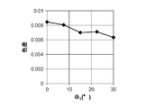
- Example 2 it is a figure which shows the relationship between the fluctuation
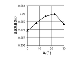
- Example 2 it is a figure which shows the relationship between the 1st angle ((theta) 1 ) and the total light beam quantity of a light-emitting device.
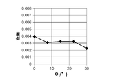
- Example 3 it is a figure which shows the relationship between the 1st angle ((theta) 1 ) and the variation value (color difference) of chromaticity by the viewing angle of the luminescent color of a light-emitting device.
- Example 3 it is a figure which shows the relationship between the 1st angle ((theta) 1 ) and the total light beam quantity of a light-emitting device.
- FIG. 1 is a cross-sectional view illustrating a configuration of a light emitting device 10 according to the first embodiment.
- the light emitting device 10 includes a substrate 100, a light emitting element 140, a first unevenness 212, and a second unevenness 232.
- the light emitting element 140 is disposed on the substrate 100, specifically, on the first surface 104 side of the substrate 100. Both the first unevenness 212 and the second unevenness 232 are arranged on the light extraction side of the light emitting element 140.
- the first irregularities 212 are arranged in the first direction.
- the second unevenness 232 is located at a location different from the first unevenness 212 in the thickness direction of the substrate 100, and intersects the first direction at a first angle (hereinafter referred to as the second direction). Listed).
- the emission spectrum of the light emitting element 140 has two or more peaks. Details will be described below.
- the substrate 100 is formed of a light-transmitting material such as glass or a light-transmitting resin.
- the substrate 100 is, for example, a polygon such as a rectangle.
- the substrate 100 may have flexibility.
- the thickness of the substrate 100 is, for example, not less than 10 ⁇ m and not more than 1000 ⁇ m.
- the thickness of the substrate 100 is, for example, 200 ⁇ m or less.
- the material of the substrate 100 includes, for example, PEN (polyethylene naphthalate), PES (polyethersulfone), PET (polyethylene terephthalate), or polyimide. Is formed. Further, when the substrate 100 includes a resin material, SiN x (silicon nitride) or SiON (silicon oxynitride) is formed on at least a light emitting surface (preferably both surfaces) of the substrate 100 in order to suppress moisture from being transmitted through the substrate 100. ) Or the like is formed.
- the light emitting element 140 is, for example, an organic EL element. Specifically, the light emitting element 140 has a configuration in which the first electrode 110, the organic layer 120, and the second electrode 130 are stacked in this order from the first surface 104 side of the substrate 100. Light emitted from the light emitting element 140 is emitted from the second surface 106 of the substrate 100 to the outside. In other words, the light extraction surface of the light emitting device 10 is the second surface 106 of the substrate 100.
- the first electrode 110 is a transparent electrode having optical transparency.
- the transparent conductive material constituting the transparent electrode is a metal-containing material, for example, a metal oxide such as ITO (Indium Tin Oxide), IZO (Indium Zinc Oxide), IWZO (Indium Tungsten Zinc Oxide), ZnO (Zinc Oxide) or the like. is there.
- the thickness of the first electrode 110 is, for example, not less than 10 nm and not more than 500 nm.
- the first electrode 110 is formed using, for example, a sputtering method or a vapor deposition method.
- the first electrode 110 may be a carbon nanotube or a conductive organic material such as PEDOT / PSS.
- the organic layer 120 has a structure in which, for example, a hole injection layer, a light emitting layer, and an electron injection layer are stacked in this order.
- a hole transport layer may be formed between the hole injection layer and the light emitting layer.
- an electron transport layer may be formed between the light emitting layer and the electron injection layer.
- the organic layer 120 may be an organic layer having a tandem structure. In this case, the organic layer 120 has a configuration in which at least two types of light emitting layers are stacked.
- the organic layer 120 has a configuration in which a hole injection layer, a light emitting layer, and an electron injection layer are repeatedly stacked in this order a plurality of times.
- An electrode or a charge generation layer may be provided between a certain hole injection layer, light emitting layer, and electron injection layer and the hole injection layer, light emitting layer, and electron injection layer thereabove.
- the emission spectrum of the light-emitting element 140 has two or more peaks.
- the light emission color of the light emitting element 140 is a color (for example, white) in which the light emission colors of the plurality of light emitting layers are mixed.
- Each of the organic layers included in the organic layer 120 may be formed by a vapor deposition method.
- at least one of these organic layers for example, a layer in contact with the first electrode 110 may be formed by a coating method such as an inkjet method, a printing method, or a spray method.
- the remaining organic layer is formed by a vapor deposition method.
- all of the organic layers described above may be formed using a coating method.
- the second electrode 130 is made of, for example, a metal selected from the first group consisting of Al, Au, Ag, Pt, Mg, Sn, Zn, and In or an alloy of a metal selected from the first group. Contains a metal layer. In this case, the second electrode 130 has a light shielding property.
- the thickness of the second electrode 130 is, for example, not less than 10 nm and not more than 500 nm. However, the second electrode 130 may be formed using the material exemplified as the material of the first electrode 110.
- the second electrode 130 is formed using, for example, a sputtering method or a vapor deposition method.
- the light emitting device 10 further has a laminated structure 200.
- the stacked structure 200 is positioned between the light emitting element 140 and the substrate 100 and has a stacked structure in which a plurality of films are stacked.
- the first unevenness 212 is located at the interface between the substrate 100 and the laminated structure 200, and the second recess 222 is located inside the laminated structure 200.
- the first unevenness 212 may also be positioned inside the laminated structure 200.
- the laminated structure 200 includes a first planarization layer 210, an inorganic layer 220, a second planarization layer 230, and a barrier layer 240.
- a plurality of first recesses 102 are formed on the first surface 104 of the substrate 100.
- the first recess 102 is formed by etching the substrate 100.
- the plurality of first recesses 102 all have substantially the same size and the same shape, and are regularly arranged two-dimensionally.
- the first planarization layer 210 is provided to fill the plurality of first recesses 102 and flatten the surface on the first surface 104 side.
- the surface of the first planarization layer 210 on the first surface 104 side enters the first recess 102.
- the first recesses and the first planarization layer 210 form the first unevenness 212. For this reason, the layout of the first unevenness 212 is determined by the layout of the first recess 102.
- the first planarization layer 210 is formed using a material having a refractive index different from that of the substrate 100 (for example, a material having a higher refractive index than the substrate 100). Therefore, the first diffraction grating is formed by the plurality of first irregularities 212.
- An inorganic layer 220 is provided on the surface of the first planarization layer 210 on the light emitting element 140 side.
- the inorganic layer 220 is formed of a light-transmitting material such as glass or a light-transmitting resin.
- the inorganic layer 220 may be a thin substrate.
- a plurality of second recesses 222 are formed on the surface of the inorganic layer 220 on the light emitting element 140 side.
- the plurality of second recesses 222 are formed by etching the inorganic layer 220.
- the plurality of second recesses 222 all have substantially the same size and the same shape, and are regularly arranged two-dimensionally.
- the second planarization layer 230 is provided to fill the second recess 222 of the inorganic layer 220 and to planarize the surface of the inorganic layer 220 on the light emitting element 140 side.
- the surface of the second planarization layer 230 on the inorganic layer 220 side enters the second recess 222.
- the second concave and convex portions 232 are formed by the second concave portions 222 and the second planarizing layer 230. For this reason, the layout of the second unevenness 232 is determined by the layout of the second recess 222.
- the second planarization layer 230 is formed using a material having a refractive index different from that of the inorganic layer 220 (for example, a material having a higher refractive index than the inorganic layer 220). For this reason, the second diffraction grating is formed by the second unevenness 232.
- the laminated structure 200 has a barrier layer 240.
- the barrier layer 240 is, for example, a SiON (silicon oxynitride) film, a SiN x (silicon nitride) film, or a laminated film thereof, and prevents moisture and the like from entering the light emitting element 140 through the laminated structure 200. Provided for.
- the first irregularities 212 are regularly arranged, and the second irregularities 232 are also regularly arranged.
- the regularity of the arrangement of the first irregularities 212 is the same as the regularity of the arrangement of the second irregularities 232.
- the graphic indicated by the arrangement of the first irregularities 212 is the same as or similar to the graphic indicated by the arrangement of the second irregularities 232.
- the direction in which the first irregularities 212 are arranged (first direction) is different from the direction in which the second irregularities 232 are arranged (second direction).
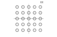
- FIG. 2 is a plan view showing a first example of the first unevenness 212
- FIG. 3 is a plan view showing a first example of the second unevenness 232.
- both the first unevenness 212 and the second unevenness 232 are arranged at lattice points of a square lattice.
- the size of the square lattice formed by the first unevenness 212 is the same as the size of the square lattice formed by the second unevenness 232.
- first unevenness 212 and the second unevenness 232 have a configuration in which convex portions are linearly provided along the lattice (in other words, portions other than the lattice are open or concave portions). You may do it.
- the 1st direction and the 2nd direction are defined as a direction parallel to one side of a square lattice, for example.
- first unevenness 212 and the second unevenness 232 overlap each other.
- the direction in which the first unevenness 212 faces (the first direction) and the direction in which the second unevenness 232 faces (the second direction) are different from each other.
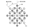
- An angle (first angle) ⁇ 1 formed by the first direction and the second direction is 10 ° to 35 °, preferably 20 ° to 25 °. In the example shown in FIG. 4, the first angle ⁇ 1 is 45 °.
- FIG. 5 is a plan view showing a second example of the first unevenness 212
- FIG. 6 is a plan view showing a second example of the second unevenness 232.
- the first unevenness 212 and the second unevenness 232 are both arranged at lattice points of a regular hexagonal lattice.
- the size of the regular hexagonal lattice formed by the first unevenness 212 is the same as the size of the hexagonal lattice formed by the second unevenness 232.
- these two hexagonal lattices may have different sizes and lattice pitches.
- the first unevenness 212 and the second unevenness 232 are provided with convex portions linearly along the lattice (in other words, portions other than the lattice are open or in the concave portions). It may have a configuration.
- a 1st direction and a 2nd direction are defined as a direction parallel to one side of a hexagonal lattice, for example.
- the first unevenness 212 and the second unevenness 232 overlap when viewed from the direction perpendicular to the substrate 100.
- the direction in which the first unevenness 212 faces (the first direction) and the direction in which the second unevenness 232 faces (the second direction) are different from each other.
- the angle (first angle) ⁇ 1 formed by the first direction and the second direction is 5 ° to 30 °, preferably 20 ° to 30 °. In the example shown in FIG. 7, the first angle ⁇ 1 is 30 °.
- the planar layout of the first unevenness 212 and the second unevenness 232 is not limited to the examples shown in FIGS.
- the first unevenness 212 and the second unevenness 232 may be provided to be another regular polygonal lattice.
- the figure drawn by the first unevenness 212 and the figure drawn by the second unevenness 232 may be different from each other.
- the light emitting device 10 has the first unevenness 212 and the second unevenness 232 between the light emitting element 140 and the second surface 106 of the substrate 100.
- Each of the first unevenness 212 and the second unevenness 232 constitutes a diffraction grating. Therefore, the light from the light emitting element 140 is easily emitted to the outside of the substrate 100, and as a result, the light extraction efficiency of the light emitting device 10 is improved.
- the emission spectrum of the light emitting element 140 has two or more peaks.
- the direction in which the first unevenness 212 faces and the direction in which the second unevenness 232 faces are different from each other. For this reason, it can suppress that the in-plane variation by the viewing angle arises in the color of the light-emitting device 10.
- FIG. 8 is a cross-sectional view illustrating a configuration of the light emitting device 10 according to the second embodiment, and corresponds to FIG. 1 in the embodiment.
- the light emitting device 10 according to the present embodiment has the same configuration as the light emitting device 10 according to the first embodiment, except that the second unevenness 302 is provided instead of the second unevenness 232.
- the second unevenness 302 is located on the second surface 106 of the substrate 100.
- the stacked structure 200 has a two-layer structure of a first planarization layer 210 and a barrier layer 240, and the inorganic layer 220 and the second planarization layer shown in the first embodiment. 230 is not provided.
- the optical film 300 is provided on the second surface 106 of the substrate 100.
- the optical film 300 has the second unevenness 302 on the surface opposite to the surface 106.
- the optical film 300 may be a film in which the second unevenness 302 is used as a microlens.
- the arrangement interval of the convex portions that become the second irregularities 302 may be 100 times or more larger than the arrangement interval of the convex portions that become the second irregularities 232.
- planar layout of the second unevenness 302 is the same as the planar layout of the second unevenness 232 shown in the first embodiment.
- the light extraction efficiency of the light emitting device 10 is improved as in the first embodiment. Further, the direction in which the first unevenness 212 faces and the direction in which the second unevenness 302 faces are different from each other. For this reason, it is possible to suppress the occurrence of in-plane variation in the color of the light emitting device 10 due to the viewing angle.
- Example 1 The light emitting device 10 having the cross-sectional structure shown in FIG. 1 and having the structure shown in FIGS. 2 to 4 as the first unevenness 212 and the second unevenness 232 was manufactured. Specifically, glass substrates were used as the substrate 100 and the inorganic layer 220. The peak of the emission spectrum of the light emitting element 140 was located in each of blue, green, and orange. Light emission from the light emitting element 140 became white. Further, as the first planarization layer 210 and the second planarization layer 230, for example, a thermosetting resin having a refractive index of 1.87 is used.
- the first unevenness 212 and the second unevenness 232 are formed by etching the substrate 100 and the inorganic layer 220, and then the first planarization layer 210 and the second planarization layer 230 are formed by, for example, heat A curable resin was formed by applying a spin coating method and then heating.
- the lattice pitch was 800 nm.
- the second unevenness 232 is provided with convex portions linearly along the lattice (in other words, the lattice portion is open or a concave portion). ing).
- the first unevenness 212 is the same as the second unevenness 232.
- the depth of the first unevenness 212 is 700 nm, and the depth of the second unevenness 232 is 850 nm.
- the area ratio of the lattice portion (the portion where no opening is formed) with respect to the first planarization layer 210 was 50%.
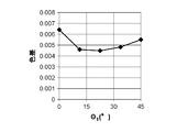
- FIG. 10 shows the relationship between the first angle ( ⁇ 1 ) and the variation value (color difference) of the chromaticity of the emission color of the light emitting device 10 when the viewing angle is changed.
- the chromaticity variation value (color difference) the chromaticity was measured when the viewing angle was changed from 0 ° to 80 ° at 10 ° intervals.
- the data shown in this figure is shown at 11.25 ° intervals.
- the color difference has become smaller.
- the color difference is further reduced, and when ⁇ 1 is 20 ° to 25 °, the color difference is particularly small.
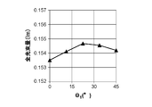
- FIG. 11 shows the relationship between the first angle ( ⁇ 1 ) and the total luminous flux of the light emitting device 10.
- the total luminous flux of the light emitting device 10 was 0.1397 lm (lumen).
- the total luminous flux of the light emitting device 10 was 0.153 lm or more. If theta 1 is 10 ° to 45 °, the total luminous flux is increased.
- ⁇ 1 is 10 ° or more and 35 ° or less, the total luminous flux of the light emitting device 10 is further increased.
- Example 2 The light emitting device 10 according to Example 2 is the same as the light emitting device 10 according to Example 1 except that the planar layout of the first unevenness 212 and the second unevenness 232 has the layout shown in FIGS. It has the same structure.
- the grating pitch was 924 nm in both the first unevenness 212 and the second unevenness 232.
- the second unevenness 232 is provided with convex portions linearly along the lattice (in other words, the lattice portion is open or in the concave portion).
- the grating depth of the first unevenness 212 is 700 nm
- the grating depth of the second unevenness 232 is 850 nm.
- the first unevenness 212 is the same as the second unevenness 232.
- the area ratio of the lattice portion (the portion where no opening is formed) with respect to the first planarization layer 210 was 50%.
- FIG. 13 shows the relationship between the first angle ( ⁇ 1 ) and the variation value (color difference) of the chromaticity of the emission color of the light emitting device 10 when the viewing angle is changed.
- the chromaticity variation value color difference
- the chromaticity was measured when the viewing angle was changed from 0 ° to 80 ° at 10 ° intervals.
- the data shown in this figure is shown at 7.5 ° intervals.
- the color difference has become smaller.
- theta 1 is in the following cases: 30 ° 25 ° or more color difference becomes particularly small.
- FIG. 14 shows the relationship between the first angle ( ⁇ 1 ) and the total luminous flux of the light emitting device 10. Also in this example, when the first unevenness 212 and the second unevenness 232 did not exist, the total luminous flux of the light emitting device 10 was 0.1397 lm (lumen). In contrast, when the first unevenness 212 and the second unevenness 232 were provided, the total luminous flux of the light emitting device 10 was 0.154 lm or more. If theta 1 is 15 ° or more than 30 °, the total light Tabaryou emitting device 10 is further increased, also, theta 1 is in the case of 20 ° or more than 30 ° total luminous flux of the light emitting device 10 becomes particularly large .
- Example 3 A light emitting device 10 having the cross-sectional structure shown in FIG. 8 and having the structure shown in FIGS. 5 to 7 as the first unevenness 212 and the second unevenness 232 was manufactured.
- the structures of the substrate 100, the light emitting element 140, and the first unevenness 212 were the same as those in Example 2.
- the optical film 300 a microlens having an arrangement pitch (center-to-center distance) of 32 ⁇ m was used.
- the height (depth) of the lens was 15 ⁇ m.
- the optical film 300 is formed using polycarbonate.
- FIG. 15 shows the relationship between the first angle ( ⁇ 1 ) and the variation value (color difference) of the chromaticity of the emission color of the light emitting device 10 when the viewing angle is changed.
- the chromaticity variation value (color difference) the chromaticity was measured when the viewing angle was changed from 0 ° to 80 ° at 10 ° intervals.
- the color difference has become smaller.
- ⁇ 1 is 15 ° or more and 30 ° or less, the color difference is further reduced, and when ⁇ 1 is 25 ° or more and 30 ° or less, the color difference is particularly small.
- a first angle (theta 1) when theta 1 showing the relationship between the total luminous flux of the light emitting device 10 is 5 ° or more than 30 °, the total luminous flux of the light emitting device 10 becomes large, theta 1 is in the case of 15 ° or more 25 ° or less total light Tabaryou emitting device 10 is further increased.
Landscapes
- Electroluminescent Light Sources (AREA)
- Non-Portable Lighting Devices Or Systems Thereof (AREA)
- Planar Illumination Modules (AREA)
- Optical Elements Other Than Lenses (AREA)
Abstract
発光素子(140)は基板(100)の上に配置されている。第1の凹凸(212)及び第2の凹凸(232)は、いずれも発光素子(140)の光取り出し側に配置されている。第1の凹凸(212)は第1の方向に並んでいる。第2の凹凸(232)は、基板(100)の厚さ方向において、第1の凹凸(212)とは異なる場所に位置しており、第1の方向と第1の角度で交わる方向(第2の方向)に並んでいる。そして、発光素子(140)の発光スペクトルは、2つ以上のピークを有している。
Description
本発明は、発光装置に関する。
発光装置の光源の一つに有機EL素子がある。有機EL素子は、2つの電極の間に有機層を配置した構成を有している。有機EL素子には、2つの電極の間に複数の有機層を有するものがある。近年は、互いに異なる色を発光する複数の有機層を重ねた構造を有する有機EL素子も提案されている。このような有機EL素子が発光する光は、発光スペクトルにおいて複数のピークを有しており、また、上記した複数の有機層の色を混ぜた色(例えば白色)になる。
一方、有機EL素子の課題の一つに、光取り出し効率の改善がある。光取り出し効率を改善する方法の一つに、有機層と光取出面の間に回折格子を設ける方法がある。特許文献1には、有機EL素子の光取り出し側に、第1の回折格子層及び第2の回折格子層を重ねて形成することが記載されている。
また特許文献2には、有機EL素子の光取り出し側に、2つ以上のモード変換手段を重ねて形成することが記載されている。モード変換手段としては、規則性のある屈折率分布を持つ光学的構造が例示されている。特許文献2の例えば図53及び図54には、2つのモード変換手段は、互いに同じ方向を向いた四方格子であること、及び、四方格子の間隔が互いに異なることが記載されている。
上記したように、有機EL素子の中には、発光スペクトルにおいて複数のピークを有するものがある。このような有機EL素子において、光取り出し効率を向上させるために回折格子を用いた場合、複数のピークの光取出効率の相対値が、視野角によって異なる可能性が出てくる。この場合、有機EL素子の発光色に面内ばらつきが生じてしまう。
本発明が解決しようとする課題としては、発光スペクトルにおいて複数のピークを有する発光素子において、光取出効率を向上させつつ、視野角による発光色の面内ばらつきを小さくすることが一例として挙げられる。
請求項1に記載の発明は、基板と、
前記基板上に配置された発光素子と、
前記発光素子の光取り出し側に配置され、第1の方向に並んだ第1の凹凸と、
前記発光素子の光取り出し側に配置され、前記基板の厚さ方向において前記第1の凹凸と異なる場所に位置し、第1の方向と第1の角度で交わる第2の方向に並んだ第2の凹凸と、
を備え、
前記発光素子の発光スペクトルは、2つ以上のピークを有する発光装置である。
前記基板上に配置された発光素子と、
前記発光素子の光取り出し側に配置され、第1の方向に並んだ第1の凹凸と、
前記発光素子の光取り出し側に配置され、前記基板の厚さ方向において前記第1の凹凸と異なる場所に位置し、第1の方向と第1の角度で交わる第2の方向に並んだ第2の凹凸と、
を備え、
前記発光素子の発光スペクトルは、2つ以上のピークを有する発光装置である。
上述した目的、およびその他の目的、特徴および利点は、以下に述べる好適な実施の形態、およびそれに付随する以下の図面によってさらに明らかになる。
以下、本発明の実施の形態について、図面を用いて説明する。尚、すべての図面において、同様な構成要素には同様の符号を付し、適宜説明を省略する。
(第1の実施形態)
図1は、第1の実施形態に係る発光装置10の構成を示す断面図である。発光装置10は、基板100、発光素子140、第1の凹凸212、及び第2の凹凸232を有している。発光素子140は基板100の上、具体的には基板100の第1面104側に配置されている。第1の凹凸212及び第2の凹凸232は、いずれも発光素子140の光取り出し側に配置されている。第1の凹凸212は第1の方向に並んでいる。第2の凹凸232は、基板100の厚さ方向において、第1の凹凸212とは異なる場所に位置しており、第1の方向と第1の角度で交わる方向(以下、第2の方向と記載)に並んでいる。そして、発光素子140の発光スペクトルは、2つ以上のピークを有している。以下、詳細に説明する。
図1は、第1の実施形態に係る発光装置10の構成を示す断面図である。発光装置10は、基板100、発光素子140、第1の凹凸212、及び第2の凹凸232を有している。発光素子140は基板100の上、具体的には基板100の第1面104側に配置されている。第1の凹凸212及び第2の凹凸232は、いずれも発光素子140の光取り出し側に配置されている。第1の凹凸212は第1の方向に並んでいる。第2の凹凸232は、基板100の厚さ方向において、第1の凹凸212とは異なる場所に位置しており、第1の方向と第1の角度で交わる方向(以下、第2の方向と記載)に並んでいる。そして、発光素子140の発光スペクトルは、2つ以上のピークを有している。以下、詳細に説明する。
基板100は、例えばガラスや透光性の樹脂などの透光性の材料で形成されている。基板100は、例えば矩形などの多角形である。ここで、基板100は可撓性を有していてもよい。基板100が可撓性を有している場合、基板100の厚さは、例えば10μm以上1000μm以下である。特に基板100をガラス材料で可撓性を持たせる場合、基板100の厚さは、例えば200μm以下である。基板100を樹脂材料で可撓性を持たせる場合は、基板100の材料として、例えばPEN(ポリエチレンナフタレート)、PES(ポリエーテルサルホン)、PET(ポリエチレンテレフタラート)、又はポリイミドを含ませて形成されている。また、基板100が樹脂材料を含む場合、水分が基板100を透過することを抑制するために、基板100の少なくとも発光面(好ましくは両面)に、SiNx(窒化シリコン)やSiON(酸窒化シリコン)などの無機バリア膜が形成されている。
発光素子140は、例えば有機EL素子である。詳細には、発光素子140は、基板100の第1面104側から、第1電極110、有機層120、及び第2電極130をこの順に積層した構成を有している。そして発光素子140の発光は、基板100の第2面106から外部に放射される。言い換えると、発光装置10の光取り出し面は基板100の第2面106である。
第1電極110は光透過性を有する透明電極である。透明電極を構成する透明導電材料は、金属を含む材料、例えば、ITO(Indium Tin Oxide)、IZO(Indium Zinc Oxide)、IWZO(Indium Tungsten Zinc Oxide)、ZnO(Zinc Oxide)等の金属酸化物である。第1電極110の厚さは、例えば10nm以上500nm以下である。第1電極110は、例えばスパッタリング法又は蒸着法を用いて形成される。なお、第1電極110は、カーボンナノチューブ、又はPEDOT/PSSなどの導電性有機材料であってもよい。
有機層120は、例えば正孔注入層、発光層、及び電子注入層をこの順に積層した構成を有している。正孔注入層と発光層との間には正孔輸送層が形成されていてもよい。また、発光層と電子注入層との間には電子輸送層が形成されていてもよい。ただし、有機層120はタンデム構造の有機層であってもよい。この場合、有機層120は、少なくとも2種類の発光層を重ねた構成を有している。具体的には、有機層120は、正孔注入層、発光層、及び電子注入層をこの順に複数回繰り返し重ねた構成を有している。ある正孔注入層、発光層、及び電子注入層と、その上の正孔注入層、発光層、及び電子注入層との間には、電極又は電荷発生層が設けられていてもよい。
そして、有機層120が有する複数の発光層のうち少なくとも2つは、互いに発光色が異なり、また、発光スペクトルのピーク位置が互いに異なる。このため、発光素子140の発光スペクトルは、2つ以上のピークを有する。その結果、発光素子140の発光色は、複数の発光層の発光色が混ざった色(例えば白色)になる。
有機層120に含まれる有機層の各々は、蒸着法で形成されてもよい。また、これら有機層のうち少なくとも一つの層、例えば第1電極110と接触する層は、インクジェット法、印刷法、又はスプレー法などの塗布法によって形成されてもよい。なお、この場合、残りの有機層は蒸着法によって形成されている。また、上記した有機層のすべてが塗布法を用いて形成されていてもよい。
第2電極130は、例えば、Al、Au、Ag、Pt、Mg、Sn、Zn、及びInからなる第1群の中から選択される金属又はこの第1群から選択される金属の合金からなる金属層を含んでいる。この場合、第2電極130は遮光性を有している。第2電極130の厚さは、例えば10nm以上500nm以下である。ただし、第2電極130は、第1電極110の材料として例示した材料を用いて形成されていてもよい。第2電極130は、例えばスパッタリング法又は蒸着法を用いて形成される。
発光装置10は、さらに、積層構造200を有している。積層構造200は、発光素子140と基板100の間に位置しており、複数の膜を積層した積層構造を有している。そして、本図に示す例において、第1の凹凸212は基板100と積層構造200の界面に位置しており、第2の凹部222は積層構造200の内部に位置している。ただし、第1の凹凸212も積層構造200の内部に位置していてもよい。
詳細には、積層構造200は、第1の平坦化層210、無機層220、第2の平坦化層230、及びバリア層240を有している。また、基板100の第1面104には、複数の第1の凹部102が形成されている。
第1の凹部102は、基板100をエッチングすることにより形成されている。複数の第1の凹部102は、いずれもほぼ同じ大きさ及び同じ形状を有しており、かつ、2次元的に規則的に配置されている。第1の平坦化層210は、複数の第1の凹部102を埋めて第1面104側の面を平坦にするために設けられている。第1の平坦化層210のうち第1面104側の面は、第1の凹部102に入り込んでいる。そして、第1の凹部102及び第1の平坦化層210によって第1の凹凸212が形成されている。このため、第1の凹凸212のレイアウトは、第1の凹部102のレイアウトによって定まる。なお、第1の平坦化層210は、基板100とは屈折率が異なる材料(例えば基板100よりも屈折率が大きい材料)を用いて形成されている。このため、複数の第1の凹凸212によって、第1の回折格子が形成される。
第1の平坦化層210のうち発光素子140側の面には、無機層220が設けられている。無機層220は、例えばガラスや透光性の樹脂などの透光性の材料で形成されている。無機層220は薄い基板であってもよい。そして、無機層220のうち発光素子140側の面には、複数の第2の凹部222が形成されている。複数の第2の凹部222は、無機層220をエッチングすることにより形成されている。複数の第2の凹部222は、いずれもほぼ同じ大きさ及び同じ形状を有しており、かつ、2次元的に規則的に配置されている。第2の平坦化層230は、無機層220の第2の凹部222を埋めて無機層220のうち発光素子140側の面を平坦にするために設けられている。第2の平坦化層230のうち無機層220側の面は、第2の凹部222に入り込んでいる。そして、第2の凹部222及び第2の平坦化層230によって、第2の凹凸232が形成されている。このため、第2の凹部222のレイアウトによって、第2の凹凸232のレイアウトが定まる。第2の平坦化層230は、無機層220とは屈折率が異なる材料(例えば無機層220よりも屈折率が大きい材料)を用いて形成されている。このため、第2の凹凸232によって、第2の回折格子が形成される。
さらに、積層構造200はバリア層240を有している。バリア層240は、例えばSiON(酸窒化シリコン)膜、SiNx(窒化シリコン)膜、又はこれらの積層膜などであり、積層構造200を介して発光素子140に水分等が侵入することを防止するために設けられる。
第1の凹凸212は規則的に配置されており、第2の凹凸232も規則的に配置されている。第1の凹凸212の配置の規則性は、第2の凹凸232の配置の規則性と同じである。言い換えると、第1の凹凸212の配置が示す図形は、第2の凹凸232の配置が示す図形と同一または相似である。そして、第1の凹凸212が並んでいる方向(第1の方向)は、第2の凹凸232が並んでいる方向(第2の方向)とは異なる。
図2は、第1の凹凸212の第1例を示す平面図であり、図3は、第2の凹凸232の第1例を示す平面図である。図2及び図3に示す例において、第1の凹凸212及び第2の凹凸232は、いずれも正方格子の格子点に配置されている。第1の凹凸212が構成する正方格子の大きさは、第2の凹凸232が構成する正方格子の大きさと同じである。
ただし、これら2つの正方格子の大きさや格子ピッチは互いに異なっていてもよい。また、第1の凹凸212及び第2の凹凸232は、格子に沿って凸部が線状に設けられた(言い換えると格子以外の部分が開口している又は凹部になっている)構成を有していてもよい。
そして、第1の凹凸212及び第2の凹凸232が正方格子を構成している場合、第1の方向及び第2の方向は、例えば正方格子の一辺に平行な方向として定義される。
図4に示すように、基板100に垂直な方向から見た場合、第1の凹凸212と第2の凹凸232は重なっている。そして、第1の凹凸212が向いている方向(第1の方向)と第2の凹凸232が向いている方向(第2の方向)は、互いに異なっている。第1の方向と第2の方向とが成す角度(第1の角度)θ1は、10°以上35°以下、好ましくは20°以上25°以下である。図4に示す例では、第1の角度θ1は、45°である
図5は、第1の凹凸212の第2例を示す平面図であり、図6は、第2の凹凸232の第2例を示す平面図である。図5及び図6に示す例において、第1の凹凸212及び第2の凹凸232は、いずれも正六方格子の格子点に配置されている。第1の凹凸212が構成する正六方格子の大きさは、第2の凹凸232が構成する六方格子の大きさと同じである。ただし、これら2つの六方格子の大きさや格子ピッチは互いに異なっていてもよい。また、第1例と同様に、第1の凹凸212及び第2の凹凸232は、格子に沿って凸部が線状に設けられた(言い換えると格子以外の部分が開口している又は凹部になっている)構成を有していてもよい。
そして、第1の凹凸212及び第2の凹凸232が六方格子を構成している場合、第1の方向及び第2の方向は、例えば六方格子の一辺に平行な方向として定義される。
図7に示すように、図5及び図6に示す例においても、基板100に垂直な方向から見た場合、第1の凹凸212と第2の凹凸232は重なっている。そして、第1の凹凸212が向いている方向(第1の方向)と第2の凹凸232が向いている方向(第2の方向)は、互いに異なっている。第1の方向と第2の方向とが成す角度(第1の角度)θ1は、5°以上30°以下、好ましくは20°以上30°以下である。図7に示す例では、第1の角度θ1は、30°である。
なお、第1の凹凸212及び第2の凹凸232の平面レイアウトは図2~図7に示した例に限定されない。例えば、第1の凹凸212及び第2の凹凸232は他の正多角格子となるように設けられていてもよい。また、第1の凹凸212が描く図形と第2の凹凸232が描く図形は互いに異なっていてもよい。
以上、本実施形態に係る発光装置10において、発光素子140と基板100の第2面106の間に第1の凹凸212及び第2の凹凸232を有している。第1の凹凸212及び第2の凹凸232は、いずれも回折格子を構成している。従って、発光素子140からの光は基板100の外部に放射されやすくなり、その結果、発光装置10の光取り出し効率は向上する。
また、発光素子140の発光スペクトルは、2つ以上のピークを有する。そして、第1の凹凸212が向いている方向と第2の凹凸232が向いている方向は、互いに異なる。このため、発光装置10の色に視野角による面内ばらつきが生じることを抑制できる。
(第2の実施形態)
図8は、第2の実施形態に係る発光装置10の構成を示す断面図であり、実施形態における図1に対応している。本実施形態に係る発光装置10は、第2の凹凸232の代わりに第2の凹凸302を有している点を除いて、第1の実施形態に係る発光装置10と同様の構成である。第2の凹凸302は、基板100の第2面106に位置している。
図8は、第2の実施形態に係る発光装置10の構成を示す断面図であり、実施形態における図1に対応している。本実施形態に係る発光装置10は、第2の凹凸232の代わりに第2の凹凸302を有している点を除いて、第1の実施形態に係る発光装置10と同様の構成である。第2の凹凸302は、基板100の第2面106に位置している。
詳細には、本実施形態において積層構造200は第1の平坦化層210及びバリア層240の2層構造になっており、第1の実施形態に示した無機層220及び第2の平坦化層230を有していない。その代わりに、基板100の第2面106には光学フィルム300が設けられている。光学フィルム300は、106とは逆側の面に第2の凹凸302を有している。光学フィルム300は、例えば第2の凹凸302がマイクロレンズとして用いられるフィルムであってもよい。この場合、第2の凹凸302となる凸部の配置間隔は、第2の凹凸232となる凸部の配置間隔よりも100倍以上大きくてもよい。
なお、第2の凹凸302の平面レイアウトは、第1の実施形態に示した第2の凹凸232の平面レイアウトと同様である。
本実施形態によっても、第1の実施形態と同様に、発光装置10の光取り出し効率は向上する。また、第1の凹凸212が向いている方向と第2の凹凸302が向いている方向は、互いに異なる。このため、視野角による発光装置10の色に面内ばらつきが生じることを抑制できる。
(実施例1)
図1に示した断面構造を有していて、第1の凹凸212及び第2の凹凸232として図2~図4に示した構造を有する発光装置10を作製した。詳細には、基板100及び無機層220としてはガラス基板を用いた。発光素子140の発光スペクトルのピークは、青色と緑色と橙色のそれぞれに位置していた。発光素子140からの発光は白色になった。また、第1の平坦化層210及び第2の平坦化層230としては、例えば屈折率が1.87となる熱硬化性樹脂を用いた。具体的には、基板100及び無機層220をエッチングにより第1の凸凹212及び第2の凸凹232を形成し、その後、第1の平坦化層210及び第2の平坦化層230を、例えば熱硬化性樹脂をスピンコーティング法で塗布した後、加熱することにより形成した。第1の凹凸212及び第2の凹凸232の双方において、格子ピッチは800nmであった。また、図9のSEM像に示されているように、第2の凹凸232は、格子に沿って凸部が線状に設けられている(言い換えると格子部分が開口している又は凹部になっている)。なお、第1の凹凸212も第2の凹凸232と同様になっている。そして、第1の凹凸212の格子の深さは700nm、第2の凹凸232の格子の深さは850nmである。第1の平坦化層210に対する格子部分(開口が形成されていない部分)の面積比は50%であった。
図1に示した断面構造を有していて、第1の凹凸212及び第2の凹凸232として図2~図4に示した構造を有する発光装置10を作製した。詳細には、基板100及び無機層220としてはガラス基板を用いた。発光素子140の発光スペクトルのピークは、青色と緑色と橙色のそれぞれに位置していた。発光素子140からの発光は白色になった。また、第1の平坦化層210及び第2の平坦化層230としては、例えば屈折率が1.87となる熱硬化性樹脂を用いた。具体的には、基板100及び無機層220をエッチングにより第1の凸凹212及び第2の凸凹232を形成し、その後、第1の平坦化層210及び第2の平坦化層230を、例えば熱硬化性樹脂をスピンコーティング法で塗布した後、加熱することにより形成した。第1の凹凸212及び第2の凹凸232の双方において、格子ピッチは800nmであった。また、図9のSEM像に示されているように、第2の凹凸232は、格子に沿って凸部が線状に設けられている(言い換えると格子部分が開口している又は凹部になっている)。なお、第1の凹凸212も第2の凹凸232と同様になっている。そして、第1の凹凸212の格子の深さは700nm、第2の凹凸232の格子の深さは850nmである。第1の平坦化層210に対する格子部分(開口が形成されていない部分)の面積比は50%であった。
図10に、第1の角度(θ1)と、視野角を変えた時の発光装置10の発光色の色度の変動値(色差)の関係を示す。色度の変動値(色差)は、正面0°から10°間隔で80°まで視野角を変えときの色度を測定した。本図に示すデータは、11.25°間隔で示されている。本図に示すように、第1の凹凸212と第2の凹凸232の向きが一致している場合(θ1=0°)と比較して、θ1が10°以上45°以下の場合、色差が小さくなった。θ1が10°以上35°以下の場合、さらに色差が小さくなり、また、θ1が20°以上25°以下の場合は色差が特に小さくなった。具体的には、θ1=0°、11.25°、22.5°、33.75°、及び45°における色差は、それぞれ0.0064、0.0046、0.0045、0.0048、及び0.0055であった。
図11に、第1の角度(θ1)と、発光装置10の全光束量の関係を示す。第1の凹凸212及び第2の凹凸232が存在しない場合(ただし積層構造200そのものは存在している)、発光装置10の全光束量は0.1397lm(ルーメン)であった。これに対して第1の凹凸212及び第2の凹凸232を設けると、発光装置10の全光束量は0.153lm以上になった。θ1が10°以上45°以下の場合、全光束量が大きくなった。θ1が10°以上35°以下の場合、発光装置10の全光束量はさらに大きくなり、また、θ1が20°以上25°以下の場合は発光装置10の全光束量が特に大きくなった。具体的には、θ1=0°、11.25°、22.5°、33.75°、及び45°における全光束量は、それぞれ0.1535lm、0.1541lm、0.1547lm、0.1545lm、及び0.1541lmであった。
(実施例2)
実施例2に係る発光装置10は、第1の凹凸212及び第2の凹凸232の平面レイアウトが図5~図7に示したレイアウトを有する点を除いて、実施例1に係る発光装置10と同様の構造を有している。本実施例において、第1の凹凸212及び第2の凹凸232の双方において、格子ピッチは924nmであった。また、図12のSEM像に示されているように、第2の凹凸232は、格子に沿って凸部が線状に設けられている(言い換えると格子の部分が開口している又は凹部になっている)。また、第1の凹凸212の格子の深さは700nm、第2の凹凸232の格子の深さは850nmである。なお、第1の凹凸212も第2の凹凸232と同様になっている。第1の平坦化層210に対する格子部分(開口が形成されていない部分)の面積比は50%であった。
実施例2に係る発光装置10は、第1の凹凸212及び第2の凹凸232の平面レイアウトが図5~図7に示したレイアウトを有する点を除いて、実施例1に係る発光装置10と同様の構造を有している。本実施例において、第1の凹凸212及び第2の凹凸232の双方において、格子ピッチは924nmであった。また、図12のSEM像に示されているように、第2の凹凸232は、格子に沿って凸部が線状に設けられている(言い換えると格子の部分が開口している又は凹部になっている)。また、第1の凹凸212の格子の深さは700nm、第2の凹凸232の格子の深さは850nmである。なお、第1の凹凸212も第2の凹凸232と同様になっている。第1の平坦化層210に対する格子部分(開口が形成されていない部分)の面積比は50%であった。
図13に、第1の角度(θ1)と、視野角を変えた時の発光装置10の発光色の色度の変動値(色差)の関係を示す。色度の変動値(色差)は、正面0°から10°間隔で80°まで視野角を変えときの色度を測定した。本図に示すデータは、7.5°間隔で示されている。本図に示すように、第1の凹凸212と第2の凹凸232の向きが一致している場合(θ1=0°)と比較して、θ1が5°以上30°以下の場合、色差が小さくなった。θ1が25°以上30°以下の場合は色差が特に小さくなった。具体的には、θ1=0°、7.5°、15°、22.5°、及び30°における色差は、それぞれ0.0040、0.0031、0.0032、0.0032、及び0.0022であった。
図14に、第1の角度(θ1)と、発光装置10の全光束量の関係を示す。本実施例においても、第1の凹凸212及び第2の凹凸232が存在しない場合、発光装置10の全光束量は0.1397lm(ルーメン)であった。これに対して第1の凹凸212及び第2の凹凸232を設けると、発光装置10の全光束量は0.154lm以上になった。θ1が15°以上30°以下の場合、発光装置10の全光束量はさらに大きくなり、また、θ1が20°以上30°以下の場合は発光装置10の全光束量が特に大きくなった。具体的には、θ1=0°、7.5°、15°、22.5°、及び30°における全光束量は、それぞれ0.1546lm、0.1547lm、0.1552lm、0.1556lm、及び0.1563lmであった。
(実施例3)
図8に示した断面構造を有していて、第1の凹凸212及び第2の凹凸232として図5~図7に示した構造を有する発光装置10を作製した。基板100、発光素子140、及び第1の凹凸212の構造は、実施例2と同様であった。また、光学フィルム300としては、配置ピッチ(中心間距離)が32μmのマイクロレンズを用いた。レンズの高さ(深さ)は15μmであった。光学フィルム300は、ポリカーボネートを用いて形成されている。
図8に示した断面構造を有していて、第1の凹凸212及び第2の凹凸232として図5~図7に示した構造を有する発光装置10を作製した。基板100、発光素子140、及び第1の凹凸212の構造は、実施例2と同様であった。また、光学フィルム300としては、配置ピッチ(中心間距離)が32μmのマイクロレンズを用いた。レンズの高さ(深さ)は15μmであった。光学フィルム300は、ポリカーボネートを用いて形成されている。
図15に、第1の角度(θ1)と、視野角を変えた時の発光装置10の発光色の色度の変動値(色差)の関係を示す。色度の変動値(色差)は、正面0°から10°間隔で80°まで視野角を変えときの色度を測定した。本図に示すように、第1の凹凸212と第2の凹凸232の向きが一致している場合(θ1=0°)と比較して、θ1が5°以上30°以下の場合、色差が小さくなった。θ1が15°以上30°以下の場合、さらに色差が小さくなり、また、θ1が25°以上30°以下の場合は色差が特に小さくなった。
図16に、第1の角度(θ1)と、発光装置10の全光束量の関係を示すθ1が5°以上30°以下の場合、発光装置10の全光束量は大きくなり、また、θ1が15°以上25°以下の場合は発光装置10の全光束量がさらに大きくなった。
以上、図面を参照して実施形態及び実施例について述べたが、これらは本発明の例示であり、上記以外の様々な構成を採用することもできる。
Claims (13)
- 基板と、
前記基板上に配置された発光素子と、
前記発光素子の光取り出し側に配置され、第1の方向に並んだ第1の凹凸と、
前記発光素子の光取り出し側に配置され、前記基板の厚さ方向において前記第1の凹凸と異なる場所に位置し、第1の方向と第1の角度で交わる第2の方向に並んだ第2の凹凸と、
を備え、
前記発光素子の発光スペクトルは、2つ以上のピークを有する発光装置。 - 請求項1に記載の発光装置において、
前記第1の凹凸は規則的に配置されており、
前記第2の凹凸は規則的に配置されている発光装置。 - 請求項2に記載の発光装置において、
前記第1の凹凸は正方格子となるように配列されており、
前記第2の凹凸は正方格子となるように配列されている発光装置。 - 請求項3に記載の発光装置において、
前記第1の角度は10°以上35°以下である発光装置。 - 請求項4に記載の発光装置において、
前記第1の角度は20°以上25°以下である発光装置。 - 請求項2に記載の発光装置において、
前記第1の凹凸は六方格子となるように配列されており、
前記第2の凹凸は六方格子となるように配列されている発光装置。 - 請求項6に記載の発光装置において、
前記第1の角度は5°以上30°以下である発光装置。 - 請求項7に記載の発光装置において、
前記第1の角度は20°以上30°以下である発光装置。 - 請求項1~8のいずれか一項に記載の発光装置において、
前記発光素子と前記基板の間に位置し、複数の膜を積層した積層構造を備え、
前記第1の凹凸は前記積層構造と前記基板の間又は前記積層構造の内部に位置しており、
前記第2の凹凸は前記積層構造の内部に位置している発光装置。 - 請求項1~8のいずれか一項に記載の発光装置において、
前記発光素子と前記基板の間に位置し、複数の膜を積層した積層構造を備え、
前記第1の凹凸は前記積層構造と前記基板の間又は前記積層構造の内部に位置しており、
前記第2の凹凸は前記基板の第2面に位置している発光装置。 - 請求項10に記載の発光装置において、
前記第2の凹凸は光学フィルムに形成されている発光装置。 - 請求項1~11のいずれか一項に記載の発光装置において、
前記発光素子の発光色は白色である発光装置。 - 請求項1~12のいずれか一項に記載の発光装置において、
前記発光素子は有機EL素子である発光装置。
Priority Applications (2)
| Application Number | Priority Date | Filing Date | Title |
|---|---|---|---|
| JP2017530578A JPWO2017017852A1 (ja) | 2015-07-30 | 2015-07-30 | 発光装置 |
| PCT/JP2015/071702 WO2017017852A1 (ja) | 2015-07-30 | 2015-07-30 | 発光装置 |
Applications Claiming Priority (1)
| Application Number | Priority Date | Filing Date | Title |
|---|---|---|---|
| PCT/JP2015/071702 WO2017017852A1 (ja) | 2015-07-30 | 2015-07-30 | 発光装置 |
Publications (1)
| Publication Number | Publication Date |
|---|---|
| WO2017017852A1 true WO2017017852A1 (ja) | 2017-02-02 |
Family
ID=57884665
Family Applications (1)
| Application Number | Title | Priority Date | Filing Date |
|---|---|---|---|
| PCT/JP2015/071702 Ceased WO2017017852A1 (ja) | 2015-07-30 | 2015-07-30 | 発光装置 |
Country Status (2)
| Country | Link |
|---|---|
| JP (1) | JPWO2017017852A1 (ja) |
| WO (1) | WO2017017852A1 (ja) |
Citations (6)
| Publication number | Priority date | Publication date | Assignee | Title |
|---|---|---|---|---|
| JP2006269294A (ja) * | 2005-03-24 | 2006-10-05 | Konica Minolta Holdings Inc | 有機エレクトロルミネッセンス素子ならびにこれを備えた照明装置および表示装置 |
| WO2008032557A1 (en) * | 2006-09-12 | 2008-03-20 | Konica Minolta Holdings, Inc. | Organic electroluminescence element, and illuminating device and display device provided with the organic electroluminescence element |
| JP2013191314A (ja) * | 2012-03-12 | 2013-09-26 | Idemitsu Kosan Co Ltd | 有機エレクトロルミネッセンス素子 |
| JP2015018822A (ja) * | 2014-09-24 | 2015-01-29 | パナソニックIpマネジメント株式会社 | 発光素子 |
| JP2015028927A (ja) * | 2013-06-27 | 2015-02-12 | 王子ホールディングス株式会社 | 有機発光ダイオード、有機発光ダイオード用基板の製造方法、画像表示装置および照明装置 |
| JP2015090810A (ja) * | 2013-11-06 | 2015-05-11 | 王子ホールディングス株式会社 | El表示装置、および、el表示装置の製造方法 |
-
2015
- 2015-07-30 JP JP2017530578A patent/JPWO2017017852A1/ja active Pending
- 2015-07-30 WO PCT/JP2015/071702 patent/WO2017017852A1/ja not_active Ceased
Patent Citations (6)
| Publication number | Priority date | Publication date | Assignee | Title |
|---|---|---|---|---|
| JP2006269294A (ja) * | 2005-03-24 | 2006-10-05 | Konica Minolta Holdings Inc | 有機エレクトロルミネッセンス素子ならびにこれを備えた照明装置および表示装置 |
| WO2008032557A1 (en) * | 2006-09-12 | 2008-03-20 | Konica Minolta Holdings, Inc. | Organic electroluminescence element, and illuminating device and display device provided with the organic electroluminescence element |
| JP2013191314A (ja) * | 2012-03-12 | 2013-09-26 | Idemitsu Kosan Co Ltd | 有機エレクトロルミネッセンス素子 |
| JP2015028927A (ja) * | 2013-06-27 | 2015-02-12 | 王子ホールディングス株式会社 | 有機発光ダイオード、有機発光ダイオード用基板の製造方法、画像表示装置および照明装置 |
| JP2015090810A (ja) * | 2013-11-06 | 2015-05-11 | 王子ホールディングス株式会社 | El表示装置、および、el表示装置の製造方法 |
| JP2015018822A (ja) * | 2014-09-24 | 2015-01-29 | パナソニックIpマネジメント株式会社 | 発光素子 |
Also Published As
| Publication number | Publication date |
|---|---|
| JPWO2017017852A1 (ja) | 2018-05-24 |
Similar Documents
| Publication | Publication Date | Title |
|---|---|---|
| US12232388B2 (en) | Electronic device | |
| TWI711176B (zh) | 有機發光顯示裝置及其製造方法 | |
| TWI799473B (zh) | 顯示面板及其製造方法 | |
| KR102072077B1 (ko) | 유기 발광 표시 장치 및 그 제조 방법 | |
| US9608045B2 (en) | Display device | |
| KR101749147B1 (ko) | 유기발광 표시장치 및 그 제조방법 | |
| TWI596748B (zh) | 顯示裝置 | |
| US8941296B2 (en) | Organic EL device having a high light output | |
| US20150372257A1 (en) | Organic light-emitting diode display panel and manufacturing method thereof | |
| KR102405943B1 (ko) | 컬러필터 어레이 기판 및 그 제조방법과 이를 이용한 유기전계발광 표시장치 | |
| KR102345872B1 (ko) | 유기 발광 표시 장치 및 유기 발광 표시 장치 제조 방법 | |
| US8283858B2 (en) | Illumination device and method for manufacturing same | |
| JP2019110118A (ja) | 有機発光表示装置 | |
| US9748525B2 (en) | Light-emitting device having reduced in-plane variation | |
| CN112864188A (zh) | 发光显示设备 | |
| CN114141966B (zh) | Oled显示面板和oled显示装置 | |
| KR102293473B1 (ko) | 유기 발광 표시 장치 및 유기 발광 표시 장치 제조 방법 | |
| CN117193551A (zh) | 触控结构、触控显示面板以及显示装置 | |
| US20120305950A1 (en) | Display apparatus | |
| CN104160783B (zh) | 发光器件的制造方法及发光器件 | |
| WO2017017852A1 (ja) | 発光装置 | |
| JP2017147042A (ja) | 発光装置 | |
| JP6457065B2 (ja) | 発光装置 | |
| WO2016016947A1 (ja) | 光学装置 | |
| WO2016059713A1 (ja) | 発光装置及び光学部材 |
Legal Events
| Date | Code | Title | Description |
|---|---|---|---|
| 121 | Ep: the epo has been informed by wipo that ep was designated in this application |
Ref document number: 15899685 Country of ref document: EP Kind code of ref document: A1 |
|
| ENP | Entry into the national phase |
Ref document number: 2017530578 Country of ref document: JP Kind code of ref document: A |
|
| NENP | Non-entry into the national phase |
Ref country code: DE |
|
| 122 | Ep: pct application non-entry in european phase |
Ref document number: 15899685 Country of ref document: EP Kind code of ref document: A1 |