WO2017017707A1 - 情報処理装置、エラー処理方法およびエラー処理プログラム - Google Patents
情報処理装置、エラー処理方法およびエラー処理プログラム Download PDFInfo
- Publication number
- WO2017017707A1 WO2017017707A1 PCT/JP2015/003734 JP2015003734W WO2017017707A1 WO 2017017707 A1 WO2017017707 A1 WO 2017017707A1 JP 2015003734 W JP2015003734 W JP 2015003734W WO 2017017707 A1 WO2017017707 A1 WO 2017017707A1
- Authority
- WO
- WIPO (PCT)
- Prior art keywords
- error
- processing
- peripheral
- information
- peripheral device
- Prior art date
- Legal status (The legal status is an assumption and is not a legal conclusion. Google has not performed a legal analysis and makes no representation as to the accuracy of the status listed.)
- Ceased
Links
Images











Classifications
-
- G—PHYSICS
- G06—COMPUTING OR CALCULATING; COUNTING
- G06F—ELECTRIC DIGITAL DATA PROCESSING
- G06F11/00—Error detection; Error correction; Monitoring
- G06F11/30—Monitoring
Definitions
- the present invention relates to an information processing apparatus, an error processing method, and an error processing program.
- a plurality of guest OSs are operated on a host OS (Operating System) using physical resources such as a plurality of CPUs and memories and a plurality of peripheral devices included in the computer.
- UE Uncorrectable Error
- the CPU is forced to interrupt and temporarily suspend the operation of the host OS.
- the operation of is also temporarily stopped.
- the guest OS that uses the failed peripheral device cannot continue to operate, the guest OS that does not use the failed peripheral device can be operated. Therefore, the failed peripheral device can be identified and operated in the shortest possible time. It is desirable to restart the guest OS.
- An object of one aspect of the present invention is to identify a failure of a peripheral device included in a computer in a short time.
- a first peripheral device accessed from a processing device via a bus is included, and the processing is performed via the first peripheral device while being connected in a tree shape starting from the first peripheral device.
- a plurality of peripheral devices accessed from the device, and a storage device that stores configuration information indicating a connection configuration of the plurality of peripheral devices, and the processing device generates an error in any of the plurality of peripheral devices.
- a plurality of peripherals located at the end opposite to the first peripheral device among the plurality of peripheral devices connected in the tree shape with reference to the configuration information stored in the storage device in response to the interrupt caused A plurality of end devices that are devices are identified, and the peripheral device that has generated the error is identified by reading out the error information and determining the presence or absence of an error preferentially from the identified plurality of end devices.
- a failure of a peripheral device included in the computer can be identified in a short time.
- FIG. 1 is a diagram illustrating a configuration example of a computer of a general Intel architecture (IA).
- FIG. 2 is a diagram illustrating an example in which two virtual machines are operated on the computer of FIG.
- FIG. 3 is a diagram illustrating an example of a system configuration of the computer according to the first embodiment.
- FIG. 4 is a diagram illustrating an example in which an error has occurred in the terminal device and the bridge device.
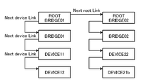
- FIG. 5 is a diagram illustrating an example of a device list.
- FIG. 6 is a diagram illustrating an example of a device list entry.
- FIG. 7 is a diagram illustrating an example of the local error register and the global error register.
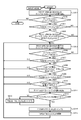
- FIG. 8 is a diagram illustrating an example of a flow of IO error handler processing.
- FIG. 1 is a diagram illustrating a configuration example of a computer of a general Intel architecture (IA).
- FIG. 2 is a diagram illustrating an example in which two virtual machines are operated on the computer of FIG.
- FIG. 9 is a diagram illustrating an example of a flow of search range selection processing.
- FIG. 10 is a diagram illustrating an example of error register value collection processing.
- FIG. 11 is a diagram illustrating a system configuration example of a computer according to the second embodiment.
- FIG. 12 is a diagram illustrating an example of an overall flow of processing for performing error register value collection processing using a plurality of CPU cores.
- FIG. 13 is a diagram illustrating an example of a flow of an error register value collection process waiting for completion.
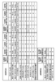
- FIG. 14 is a diagram illustrating an example of initial values of the device list.
- FIG. 15 is a diagram illustrating a transition example 1 of the device list.
- FIG. 16 is a diagram illustrating a second transition example of the device list.
- FIG. 15 is a diagram illustrating a transition example 1 of the device list.
- FIG. 17 is a diagram illustrating an example of a device change information interface.
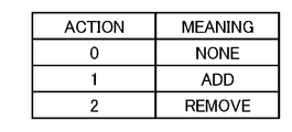
- FIG. 18 is a diagram illustrating an example of the value of the “ACTION” field of the device change information interface.
- FIG. 19 is a diagram illustrating an example of a device list after device deletion.
- FIG. 20 is a diagram illustrating an example of a device list after adding a device.
- FIG. 21 is a diagram illustrating an example of a system configuration diagram according to the third embodiment.
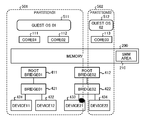
- FIG. 1 is a diagram illustrating a configuration example of a computer 10 of a general Intel architecture (IA).
- a PCI device is mounted in addition to the CPU 100 and the memory 200.
- the PCI device is included in a PCI peripheral block 400 and is accessed from the CPU 100 via the bus 300.
- the CPU 100 has CPU cores 111, 112, and 113. Each of the CPU cores 111 to 113 executes a program stored in the memory 200, thereby executing processing of an operating system (OS) and application programs operating on the OS.
- the CPU of Intel Architecture (IA) has an operation mode different from a normal operation called System Management Mode (SMM) in addition to a normal operation mode that is an operation mode for processing application programs.
- FIG. 1 schematically shows that each of the CPU cores 111 to 113 has a corresponding SMM processing unit 121, 122, 123.
- SMI System113Management ⁇ Interrupt
- the memory 200 includes an SMM area 210.
- the SMM area 210 is a dedicated memory area for storing a program for the CPU cores 111 to 113 to operate in the SMM mode, and includes an IO error handler 220.
- Each of the CPU cores 111 to 113 executes processing in the SMM mode by executing a program included in the IO error handler 220 or the like stored in the SMM area 210 when the CPU core 111-113 transitions to the SMM mode.
- the bridge devices 421 and 422 and end devices (End-devices) 431 to 434 located at the ends of the tree are connected by a PCI bus in a tree shape starting from the root bridge devices 411 and 412.
- the terminal devices 431 to 434 include, for example, an interface device such as a LAN (Local Area Network) card device or a RAID (Redundant Arrays of Independent Disks) card.
- a tree structure connected by a PCI bus starting from the root bridge device is also called a PCI bus tree.
- Each PCI device included in the PCI bus tree has a “local error register”.
- Each local error register is a register that stores information about an error that has occurred when an error occurs in each PCI device. An example of the local error register will be described later with reference to FIG.
- the root bridge device 421, 422 which is the starting point of the PCI bus tree, is notified of the error.
- the error information notified to the root bridge devices 421 and 422 is stored in a specific register (hereinafter referred to as “global error register”) included in the root bridge devices 421 and 422.
- the global error register holds information indicating whether an error has occurred in either the bridge device or the terminal device under the root bridge device.
- Information stored in the global error register is referred to when the CPU cores 111 to 113 check on which PCI bus tree an error has occurred. An example of the global error register will be described later with reference to FIG.
- the PCI device in which an error has occurred is specified and error information is output.
- a recovery process is also executed in some cases.
- UE uncorrectable error
- UE uncorrectable error
- the OS cannot operate normally unless the cause of the device error is resolved. Therefore, it is not necessary to immediately return from the SMM mode to the normal operation mode in a state where the device error is not eliminated.
- FIG. 2 is a diagram showing an example in which two virtual machines are operated on the computer 10 of FIG.
- a partition 501 (PARTITION 01) and a partition 502 (PARTITION 02) are provided by using hardware resources (CPU core, memory, PCI device, etc.) of the computer 10.
- the partitions 501 and 502 can be logical partitions, for example.
- a partition 501 includes CPU cores 111 and 112 and a part of the memory 200, a PCI device tree starting from the root bridge device 411, and a terminal device connected via the root bridge device 412 and the bridge 422. 433 is included.
- the partition 502 includes a CPU core 113 and a part of the memory 200, and a root device 434 connected via a root bridge device 412 and a bridge 422.
- a virtual machine (not shown) is operated by physical resources included in the partition 501, and the guest OS 511 (GUEST OS 01) is executed on the virtual machine.
- the guest OS 511 (GUEST OS 01) is executed on the virtual machine.
- a virtual machine (not shown) is operated using physical resources (CPU core 113, terminal device 434, etc.) included in the partition 502, and a guest OS 512 (GUEST OS 02) is executed on the virtual machine. Is done.
- each CPU core 111 to 113 transitions to SMM, and the guest The operations of the OSs 511 and 512 are temporarily stopped.
- the guest OS 511 since an error has occurred in the terminal device 433 included in the partition 501, it is difficult to continue operation unless the error is resolved.
- the guest OS 512 since no error has occurred in the hardware resources included in the partition 502, the operation can be continued. In this case, there is a concern that the operation of the guest OS 512 is temporarily stopped while the CPU cores 111 to 113 are in the SMM mode.
- an error occurs in one CPU core (for example, CPU core 111) among CPU cores 111 to 113 that have shifted to the SMM mode.
- a process of specifying the PCI device that has been performed is performed.
- the CPU core 111 searches for PCI devices included in the PCI bus tree from, for example, the root bridge devices 411 and 412 and identifies all connected PCI devices.
- the search for the PCI device starts from the bus number assigned to the root bridge devices 411 and 412, for example, and sequentially increases the bus number, the device number, and the function number. Check if it exists.
- the presence confirmation of the PCI device is performed, for example, by actually trying to access the PCI device register corresponding to those numbers and judging from the access response result.
- the CPU core 111 reads the value of the local error register included in all the PCI devices, and identifies the PCI device that caused the error based on the read information.
- the CPU core 111 performs a recovery process on the specified PCI device if possible, but there is almost no recovery method if the error is caused by a hardware failure. To notify the occurrence of an error.
- the number of PCI devices included in the PCI peripheral block 400 is small for ease of explanation. However, depending on the system configuration of the computer 10, several tens to several hundreds. PCI devices may be included in the PCI peripheral block 400.
- the above-described PCI device search method can cope with the configuration of an arbitrary PCI bus tree, but requires more processing time as the number of PCI devices to be searched increases.
- Example 1 will be described with reference to FIGS.
- FIG. 3 is a diagram illustrating a system configuration example of the computer 20 according to the first embodiment.
- the computer 20 has a CPU 100, a memory 200, and a PCI peripheral block 400, and the CPU 100 accesses the memory 200 and the PCI peripheral block 400 via the bus 300.
- Components having the same reference numerals such as PCI devices included in the CPU 100 and the PCI peripheral block 400 are the same as those described in FIG.
- the PCI device that caused the error is specified based on the connection configuration of the PCI device. Specifically, first, configuration information indicating a connection configuration of PCI devices existing in the PCI bus tree for each root bridge device, that is, a device list 330 indicating position information of the PCI devices on the PCI bus tree is displayed. Create it. Based on the created device list 330, information on the local error register of the terminal device is collected from the terminal device included in the PCI bus tree to be searched.
- End Device located at the end of the tree shape among PCI devices included in the PCI device tree.
- End Device located at the end of the tree shape among PCI devices included in the PCI device tree.
- the end devices 431 to 434 including the LAN card device and the RAID card device are more complicated in function than the bridge devices 421 and 422 and the root bridge devices 411 and 412, so that a hardware failure is also caused. This is because it is likely to occur.
- the presence / absence of an error is preferentially checked from the end device (End ⁇ ⁇ ⁇ Device) where an error is likely to occur among the PCI devices included in the PCI device tree. This is because collection of local error registers such as the remaining bridge devices can be omitted when an error can be identified by the terminal device. If the location of the error cannot be identified by referring to the local error register information of all end devices, local errors of the remaining PCI devices such as bridge devices connected to the upper side of the tree above each end device ⁇ Collect register information and identify errors.
- the SMM error processing method in the SMM includes an IO error handler 220, a device list 230, and a device list creation unit 241 in the SMM area 210 in order to confirm whether or not an error has occurred preferentially from the terminal device.
- the device list creation unit 241 creates a device list 330 on the SMM area 210.
- the device list creation unit 241 is called by, for example, BIOS (Basic Input / Output System) when the computer 20 is started up.
- BIOS Basic Input / Output System
- the device list creation unit 241 searches for each PCI device by a conventional PCI device search method to find a PCI device. For example, starting from the bus numbers assigned to the root bridge devices 411 and 412, the bus number, device number, and function number are sequentially increased, and it is confirmed whether there is a PCI device that matches those numbers. .
- a device list creation unit 241 Every time a device list creation unit 241 finds a PCI device, it creates an entry corresponding to the found device (hereinafter referred to as “device list entry”). Then, the created device list entry is added to the device list 230. Then, the device list creation unit 241 stores the created device list 230 in, for example, the SMM area 210 in the memory 200.
- the device list 230 will be described later with reference to FIG.
- the IO error handler 220 called in the SMM mode includes a search range selection unit 221, an error register value collection unit 222, an error location identification unit 223, and an error handling unit 224.
- the search range selection unit 221 initializes the device list 230 and selects a PCI root bridge device to be searched.
- the error register value collection unit 222 collects error register information from the PCI device based on the device list 230. The collection of error register values by the error register value collection unit 222 is also executed by collecting error register information using a plurality of CPU cores described later.
- the error location specifying unit 223 specifies a device in which an error has occurred based on the read error register information.
- the error handling unit 224 performs recovery processing for a device that has generated an error if recovery is possible when the device that has generated the error is identified. In many cases, it is not possible to perform recovery processing of a device that has caused an error. In this case, only notification of error information is performed to an external management device or the like.
- Each function block included in the device list creation unit 241 and the IO error handler 220 included in the SMM area 210 is executed by the CPU cores 111 to 113 included in the CPU 100, thereby realizing each function.
- each of the CPU cores 111 to 113 transitions to the SMM mode, and the program included in the IO error handler 220 is executed. Specifically, a device error is specified by the search range selection unit 221, the error / register value collection unit 222, and the error location specification unit 223 included in the IO error handler 220. At that time, error information is preferentially collected from the terminal devices included in the PCI bus tree using the device list 230 created in advance. By specifying the presence / absence of an error preferentially from the end device (End Point) included in the PCI device tree, the PCI device in which the error has occurred can be identified more efficiently, and the failure of the peripheral device included in the computer can be identified. It can be identified in a short time.
- End Point End Point
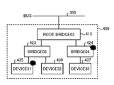
- FIG. 4 is a diagram showing an example in which an error occurs in the terminal device and the bridge device.
- FIG. 4 shows an example in which an error has occurred at two locations of the bridge device 424 and the terminal device 435.
- the range of influence varies depending on the degree of the error.
- the terminal device 437 which is a device under the bridge device 424, cannot be accessed. Therefore, in this embodiment, when a terminal device that cannot perform register access is found, error information of the bridge device to which the terminal device that could not be accessed is also collected after collecting error information of the terminal device. Collect. By doing so, errors in the bridge device can be collected without overlooking.
- the error of the bridge device 424 is a slight error that allows access to the devices under the bridge device 424
- the error of the bridge device 424 is overlooked once by finding the error of the terminal device 435 first.
- the interrupt by the SMI is raised again after exiting the SMM mode, and the error identification processing in the SMM is performed. Is detected by In this case, the error that is overlooked is temporary because the error symptom is mild and the error itself is very rare at the same time, and it can be detected again even if it is overlooked.
- the influence of the error in the bridge device 424 that was overlooked is small.
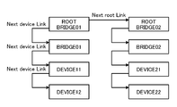
- FIG. 5 is a diagram showing an example of the device list 230.
- a “device list entry” corresponding to a PCI device existing under the root bridge device is shown in a diagram in which the root bridge device is connected in a list structure.
- An example of the contents of the device list 230 will be described later with reference to FIG.
- the labels such as “ROOT BRIDGE01” displayed in each entry correspond to the labels displayed in FIG. 1 and FIG.
- the entry labeled “ROOT BRIDGE01” corresponds to the root bridge device 411 shown in FIG.
- Each device under the root bridge device is connected by an arrow “Next device Link”, and “ROOT BRIDGE01” to “ROOT BRIDGE02” is connected by an arrow “Next root Link”.
- FIG. 6 is a diagram illustrating an example of a device list entry included in the device list 230.
- the device list entry of each PCI device information of each entry shown in the left frame of FIG. 6 is set.
- An example of each element of the device list entry will be described below.
- ROOT FLAG is set to the value 1 when the device corresponding to the entry is a root bridge device. If the device corresponding to the entry is other than the root bridge device, the value 0 is set. The value of “ROOT ⁇ FLAG” is set when a device list entry is created or updated.
- ROOT DATA POINTER is a pointer to “Root Data” which is extended data for the root bridge device. “Root Data” will be described later.
- NEXT DEVICE DEVICE LINK refers to the next “device list entry” under the same root bridge device. “NEXT DEVICE LINK” is set when a device list entry is created or updated.
- LOCATION indicates device location information.
- the device position information includes, for example, a segment number, a bus number, a device number, and a function number. “LOCATION” is set when a device list entry is created or updated.
- END DEVICE FLAG is set to a value of 1 when the device corresponding to the entry is an end device. If the device corresponding to the entry is not a terminal device, the value 0 is set. “END DEVICE FLAG” is set when a device list entry is created or updated.
- DISABLE FLAG is information indicating that an error is not searched, and a device with a value of 1 in “DISABLE ⁇ FLAG ”is not searched for an error.
- “DISABLE FLAG” is initialized with a value of 0 when a device list entry is created or updated.
- “READ-FAIL FLAG” is set to a value of 1 when the PCI device register cannot be read. For example, even when an error occurs in the bridge device and the register of the subordinate device cannot be read, the value “1” is set in “READ-FAIL FLAG” of the entry of the device that could not read the register. “READ-FAIL FLAG” is initialized to 0 by the search range selection unit 221.
- “COMPLETE FLAG” is set to 1 when reading of the error register from the device is complete. The value is 0 until the reading of the error register from the device is completed. “COMPLETE FLAG” is initialized to 0 by the search range selection unit 221, and 1 is set by the error register value collection unit 222.
- ERP FLAG is set to 1 when there is an error in the device corresponding to the entry. “ERROR FLAG” is initialized to 0 each time the search range selection unit 221 searches for an error of the PCI device.
- “UPDATING LOCK” is a spin lock variable for exclusive access to the device corresponding to the entry. “UPDATING LOCK” is used when the error register value collection unit 222 acquires a lock before reading the error register of the device and releases the lock after completion. For example, when the value 1 is set, the spin lock variable indicates that any of the CPU cores 111 to 113 that may access the device corresponding to the entry has acquired the lock. If a CPU core reads a value of “UPDATING LOCK” and the value is 0, it means that another CPU core has not acquired the lock, so the lock has been successfully acquired and the value 1 is set.
- ERP Error REGISTERS DUMP
- ERRORISTREGISTERS DUMP is an area to store the read error register value. Since the number of error registers to be read depends on the system configuration, the size of the area of “ERRORISTREGISTERS DUMP” is arbitrary.
- ERP Error REGISTERS DUMP
- search range selection unit 221 a value is set by the error register value collection unit 222.
- Root Data includes “NEXT ROOT LINK”, “GLOBAL ERROR FLAG”, “DETECTED ERROR FLAG”, and “CHECK ALL FLAG”.
- NONE ROOT LINK indicates the device list entry of the next root bridge device. If there is no entry for the next root bridge device, the value 0 is set. “NEXT ROOT LINK” is set when a device list entry is created or updated.
- GLOBAL ERROR FLAG is set to 1 when an error occurs in a device under the root bridge device. “GLOBAL ERROR FLAG” is set every time the search range selection unit 221 selects a PCI root bridge device.
- ERROR DETECTED COUNT is incremented by 1 each time an error is detected in a device under the root bridge device. “ERROR DETECTED COUNT” is initialized to 0 each time the search range selection unit 221 searches for an error of the PCI device.
- CHECK FLAG is set to 1 when it is necessary to specify not only the end device but also the bridge device. “CHECK ALL FLAG” is initialized to 0 each time the search range selection unit 221 searches for an error of the PCI device.
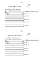
- FIG. 7 is a diagram showing an example of the local error register and the global error register.
- FIG. 7A shows an example of the local error register 610.
- the local error register 610 is a register that is provided in each PCI device and stores information regarding the error that has occurred when an error occurs in each PCI device.
- the local error register 610 includes a plurality of UE status registers 611-1 to 611-M (M is a natural number) and a plurality of CE status registers 612-1 to 612-L (L Is a natural number).
- UE status registers 611-1 to 611-M indicate whether or not an uncorrectable error (UE: Uncorrectable Error) has occurred, and each bit of N (N is a natural number) is an error for each error type (Type) Indicates the presence or absence of occurrence.
- CE status registers 612-1 to 612-L indicate whether or not a correctable error (CE: Correctable Error) has occurred.
- the CE status registers 612-1 to 612-L can also be implemented to include, for example, a bit indicating whether or not N CEs have occurred.
- Information stored in the local error register 610 is read by the error register value collection unit 222.
- a plurality of registers indicating whether or not each error of UE and CE has occurred is provided.
- the numbers M and L of the registers are the causes and types of errors occurring in the PCI device. Depending on the number, it can be any number.
- FIG. 7A shows an example in which the local error register holds various types of error information, but error information is part of the status register that holds other status information of the device. Can also be held. In that case, the error register value collection unit 222 reads information related to the error from the status register of each PCI device.
- FIG. 7B is a diagram illustrating an example of the global error register 620.
- the global error register 620 is a register provided in each root bridge device, and holds information indicating whether an error has occurred in either the bridge device or the terminal device under the root bridge device.
- the global error register 620 includes a plurality of global UE status registers 621-1 to 621-Y (Y is a natural number) and a plurality of global CE status registers 622-1 to 622-Z. (Z is a natural number).
- Y is a natural number
- Z is a natural number
- the global UE status registers 621-1 to 621-Y and the global CE status registers 622-1 to 622-Z as in the case of the local error register 610, whether or not an error has occurred for each of the N types of errors. Can be implemented to include a bit representing.
- the UE Type () of one of the global UE status registers 621-1 to 621-Y of the root bridge device The bit corresponding to 1) is set.
- the number of Y and Z can be set arbitrarily according to the mounting of the PCI device.
- FIG. 8 is a diagram illustrating an example of the flow of the IO error handler process according to the first embodiment.
- the root bridge device of the PCI bus tree including the device with the error is specified.
- the search range selection unit 221 identifies the root bridge device of the PCI bus tree including the initialization of the device list 230 and the device in which the error has occurred. Details of the processing of S101 will be described later with reference to FIG.
- S102 it is determined whether or not to continue the process of specifying the error location of the PCI device. If the value of “GLOBAL ERROR FLAG” of all the root bridge device entries specified by the device list 230 is “0” (NO in S102), there is no PCI device error, and the process proceeds to S108. On the other hand, if the value of “GLOBAL ERROR FLAG” of the entry of any root bridge device is “1” (YES in S102), the process proceeds to S103.
- the error register value collection unit 222 collects the values of the local error registers of the devices under the root bridge device whose “GLOBAL ERROR FLAG” value is “1”.
- the error register value collecting unit 222 preferentially collects error information from the local error register of the terminal device.
- a terminal device End Device
- the device list 230 created in advance by the device list creation unit 241, and error information is preferentially collected from the terminal device.
- the processing by the error register value collection unit 222 in S103 will be described using the processing flow of FIG. 10 or FIG. FIG. 12 described later illustrates a processing flow for enabling the error / register value collection unit 222 to be executed by a plurality of CPU cores. However, when the processing is performed by one CPU core, the processing of S401 is omitted. Good.
- the processing of FIG. 12 is called from S103 or S107 of FIG.
- the difference between S103 and S107 is that the value specified for “mode” is different.
- the process of FIG. 10 is called from S402 and S405 of FIG. 12
- the value of the “mode” designated when the process of FIG. 12 is called in S103 or S107 of FIG.
- the error location identifying unit 223 identifies the PCI device that caused the error based on the local error register information of the end device (End ⁇ Device) collected in the process of S103. For a device that has caused an error, set a value of 1 to the “ERROR FLAG” of the device list entry corresponding to that device, and set the “ERROR DETECTED COUNT” of the device list entry of the root bridge device. Increase the value by one.
- S105 it is determined whether or not to continue the process of identifying the error part of the device. Specifically, for the root bridge device with “GLOBAL ERROR FLAG” value of “1” in the device list 230, identification of the error location is continued based on the values of “ERROR DETECTED COUNT” and “CHECK ALL FLAG”. Determine whether to do. If it can be determined from the count value of “ERROR ⁇ ⁇ ⁇ DETECTED COUNT” that an error has occurred in any of the end devices (YES in S105), the error information collection process is terminated and the process proceeds to the error handling process in S108. However, if the value of “CHECK ALL FLAG” is 1, there is a possibility that the bridge device also has an error, so the process proceeds to S106.
- the error location identifying unit 223 identifies the PCI device that caused the error based on the information in the local error register such as the bridge device collected in the process of S106. Finally, in S107, the error location including the error of the bridge device is specified. In the present embodiment, by using the device list 230, it is possible to collect information on the error register step by step with priority given to the end device.
- FIG. 9 is a diagram showing an example of the flow of search range selection processing.
- the search range selection unit 221 first initializes the device list 230 in S201.
- “READ-FAIL FLAG”, “COMPLETE FLAG”, “ERROR FLAG” and “ERROR REGISTERS DUMP” areas are initialized with the value 0 for all device list entries.
- “Root Data”, “GLOBAL ERROR FLAG”, “ERROR DETECTED COUNT”, and “CHECK ALL FLAG” are initialized with the value 0.
- the search range selection unit 221 extracts the device list entry of the root bridge device from the device list 230 in S202.
- the device list entry of the root bridge device is extracted by following “NEXT ROOT LINK” from the entry of the head root bridge device. If there is no root bridge device that has not been checked for errors in the device list entry of the root bridge device (NO in S203), the processing of FIG. 9 is terminated, and the device list entry of the root bridge device is completed. If there is, it is determined whether or not “DISABLE FLAG” is set in S204.
- the global error register and local error register of the root bridge device are read based on the information of “LOCATION”, the read result is stored in the area of “ERROR REGISTERS DUMP”, and “COMPLETE FLAG” is set as the value. 1 is set (S206). If the information of the global error register and the local error register of the root bridge device cannot be read normally in S205 (NO in S207), the value 1 is set to “READ-FAIL FLAG” (S208), The process proceeds to S213.
- the process proceeds to S209. If the information read from the global error register does not include information indicating that there is an error (NO in S209), the process returns to S202 and proceeds to the error determination process of the next root bridge device.
- the process returns to S202 to search for the next root bridge device. If it is determined from the information in the local error register of the root bridge device that there is an error in the root bridge device itself (YES in S212), the device list entry “ERROR FLAG” of the root bridge device itself is set to the value 1. (S213). Then, the value of “ERROR DETECTED COUNT” is increased by 1 (S214). And it returns to the process of S202 and searches for the next root bridge apparatus.
- the device list 230 is initialized and the root bridge device having error information is specified by the above-described processing of FIG.
- FIG. 10 is a diagram showing an example of error register value collection processing.
- Each process of FIG. 10 is a process executed by the error register value collection unit 222, and collects error register information from the PCI device based on the device list 230.
- a variable of mode (MODE) is designated by an argument.
- the value of the mode specified by the argument is 1, only the end device (End Device) is the collection target of the error register information, and when the mode value is 2, all the PCI devices are collected.
- the device list entry of the root bridge device is extracted from the device list 230.
- the error / register value collection unit 222 takes out the entry of the head root bridge device immediately after calling the processing flow of FIG.
- the entry of the root bridge device is taken out by following “NEXT ROOT LINK”.
- the processing of S304 determines whether or not there is an error in the device under the root bridge device by checking whether or not the value of “GLOBAL ERROR FLAG” is 1 in the device list entry of the root bridge device. . If the value of “GLOBAL EROR FLAG” is not 1 (NO in S304), it means that no error was found in the device under the root bridge device, so the process returns to S301, and the device of the next root bridge device Proceed to list entry retrieval processing.
- the mode setting is 1 (only the terminal device is targeted) and “END DEVICE FLAG” of the target device is 1, or the mode Is set to 2 (all devices are targets) (S308). If none of the cases in S308 is applicable (NO in S308), the error register value is not collected, and the process returns to S305.
- the error register value of the target device that is, the local error register information is read and stored in the “ERROR REREGERS DUMP” area of the target device. If the information in the local error register cannot be read normally (NO in S312), “READ-FAIL FLAG” of the target device is set to a value 1 (S313).
- step S312 If YES in step S312, or after the processing in step S313, “COMPLETE FLAG” of the target device is set to a value 1 (S314), “UPDATING LOCK” is canceled, and the exclusive processing is terminated (S315). Return to the process.
- the device list 230 including the PCI device position information is created. Then, based on the information in the created device list 230, the presence / absence of an error occurrence is specified preferentially from the end device (End Point) included in the PCI device tree.
- End Point End Device
- the PCI device in which the error has occurred can be specified more efficiently, and the failure of the peripheral device included in the computer can be prevented in a short time. Can be specified.
- FIG. 11 is a diagram illustrating a system configuration example of the computer 30 according to the second embodiment.
- the memory 200 stores a program for performing processing of the hypervisor 250.
- the SMM area 210 included in the memory 200 includes a device list update unit 242 and a device change information I / F unit 243 in addition to the components shown in FIG.
- the hypervisor 250 manages virtual machines running on the CPU cores 111 to 113. Further, the hypervisor 250 detects the PCI hot plug of the guest OSs 511 and 512.
- the hypervisor 250 includes a device change notification unit 251.
- the device list update unit 242 receives a device change information via the device change information I / F unit 243. Notify that there has been a change.
- the device list update unit 242 updates the contents of the device list 230 based on the information notified from the device change notification unit 251.
- the process of the device list update unit 242 is a process executed when a device is added or deleted by PCI hot plug or the like, for example.
- the device change notification unit 251 sets information about the changed device in the storage area included in the device change information I / F unit 243, and then sets each CPU core 111 to 113. Increase the SMI.
- each of the CPU cores 111 to 113 receives an SMI interrupt, it shifts to the SMM mode and calls the processing by the device list update unit 242.
- the device list update unit 242 refers to the information set in the storage area of the device change information I / F unit 243, determines whether or not a PCI device is added or deleted, and the contents of the device list 230 Update.
- a ROM (Read Only Memory) 280 is added in addition to the components shown in FIGS.
- the ROM stores a program for performing processing of the device list creation unit 241, a program for performing processing of the IO error handler 220, and the like.
- the program stored in the ROM is expanded in an area on the memory 200 when the system of the computer 30 is activated, and is executed by the CPU cores 111 to 113.
- the device list creation unit 241 searches for a PCI device included in the system of the computer 30 when expanded on the memory 200. As a result of searching for a PCI device, each time a PCI device is found, a device list entry corresponding to the found device is created in the device list 230. When the search for the PCI device and the creation of the device list entry by the device list creation unit 241 are completed, the device list 230 shown in FIG. 5 is created.
- an SMI interrupt is raised in each of the CPU cores 111 to 113 in the computer 30, and each of the CPU cores 111 to 113 Transition to mode.
- a search is performed for a PCI device in which an error has occurred after each CPU core 111 to 113 has shifted to the SMM mode.
- a plurality of CPU cores need to be searched rather than a single CPU core. Those who share can be discovered sooner.
- “COMPLETE FLAG” for determining the information collection status of the error register from each PCI device and each CPU core 111 to 113 perform processing exclusively. Includes an entry for “UPDATING LOCK”.
- “COMPLETE FLAG” and “UPDATING LOCK” it is possible to collect error register information in parallel using a plurality of CPU cores 111 to 113. This can reduce the time to collect error registers from many PCI devices.
- FIG. 12 is a diagram showing an example of the overall flow of processing by the error / register value collection unit 222 using a plurality of CPU cores.
- S401 to S403 on the left side are processes by the representative CPU core
- S404 to S406 are processes by other CPU cores.
- the representative core is, for example, one CPU core among the plurality of CPU cores 111 to 113, and controls error register collection processing by other CPU cores.
- the representative CPU core transmits a request for requesting another CPU core to collect an error register value (S401). ).
- the representative CPU core may transmit a request for requesting processing for collecting error register values to a plurality of other CPU cores.
- the representative CPU core itself also performs processing for collecting error register values (S402).
- the process of FIG. 10 is called by specifying a mode argument.
- the other CPU cores wait for a request for requesting processing for collecting the error register value from the representative CPU core (S404), and upon receiving the request, perform processing for collecting the error register value (S405). Even in the process of collecting the error register values in S405, the other CPU cores that have received the request specify the mode argument and call the process of FIG. When the error register value reading process in S405 is completed, the other CPU cores wait for the next request from the representative CPU core to be transmitted (S406).
- the representative core waits for completion of the error register value collection process by other CPU cores (S403). Specifically, the representative CPU core designates a mode (Mode) and calls the processing of FIG.
- FIG. 13 is a diagram showing an example of a processing flow in which the representative CPU core in FIG. 12 waits for the end of error / register value collection processing by a plurality of other CPU cores.
- the process of FIG. 13 illustrates the process called from S403 of FIG.
- the representative CPU core first extracts the device list entry of the root bridge device from the device list 230 (S501).
- the device list entry of the root bridge device in S501 can be extracted by first extracting the entry of the first root bridge device and tracing the “NEXT ROOT LINK” after the second time.
- the processing of S504 determines whether there is an error in the device under the root bridge device by checking whether the value of “GLOBAL ERROR FLAG” is 1 in the device list entry of the root bridge device. . If the value of “GLOBAL EROR FLAG” is not 1 (NO in S504), no error is found in the device under the root bridge device, so the process returns to S501, and the device of the next root bridge device Proceed to list entry retrieval processing.
- the mode setting is 1 (only the terminal device is the target) and “END DEVICE FLAG” of the target device is 1, or the mode Is set to 2 (all devices are targets) (S508). If none of the cases in S508 is applicable (NO in S508), the error register is not collected, and the process returns to S505.
- the time for collecting error register values from many PCI devices by collecting error register values using a plurality of CPU cores including the representative CPU core. Can be shortened.
- FIG. 14 is a diagram showing an example of the initial value of the device list.
- the device list 230 may be held in a table format in which a device list entry of each device is stored in each column using a plurality of rows.
- each device in the device list 230 Since the actual data of the device list 230 is stored in the memory 200, an address address is assigned to each device in the device list 230, and pointers such as “NEXT DEVICE LINK” and “NEXT ROOT LINK” are also addressed. By storing the address, the destination indicated by the pointer can be set.
- the initial value of each device list entry shown in FIG. 14 stores the initial value described in the description of FIG.
- FIG. 15 is a diagram showing a transition example 1 of the device list.
- FIG. 16 is a diagram illustrating a second example of device list transition.
- the error search process in the SMM mode is performed in parallel using the three CPU cores 111 to 113.
- the CPU core 111 executes the processing of the IO error handler 220 according to the flow of FIG. 8 in the SMM mode.
- the CPU core 111 executes search range selection processing (S101) in FIG.
- search range selection processing S101
- the error information is notified to the root bridge device 412 (ROOT12BRIDGE02) of the PCI bus tree to which the terminal device 433 belongs.
- information for example, value 1 indicating that there is an error in the global error register of the root bridge device 412 is set.
- FIG. 15 shows an example of the device list 230 after the processing of S101 of FIG. 8, specifically, the error information collection processing of the root bridge device by the search range selection unit 221 shown in FIG.
- “COMPLETE FLAG” of the root bridge device 411 (ROOT BRIDGE01) and the root bridge device 412 (ROOT BRIDGE02) is set to 1.
- “GLOBAL ERROR FLAG” of the root bridge device 412 (ROOT BRIDGE 02) is set to 1.
- the CPU core 111 determines to continue the process of identifying the error location in S102 of FIG. 8 (YES in S102). Then, the CPU core 111 performs error register value collection processing of the terminal device in S103 of FIG. At this time, the CPU 111 sets the mode argument to 1 and calls the processing of FIG.
- the CPU 111 as the representative CPU core transmits a request for collecting error register values to the other CPU cores 112 and 113 that are waiting in accordance with the processing flow of FIG. 12 (S401). Then, the error register value collection process of S402 by the representative CPU core 111 and the error register value collection process of S405 by the other CPU cores 112 and 113 are executed in parallel.
- FIG. 16 shows an example of the device list 230 after the representative CPU core 111 executes the processing up to S403 in FIG.
- the presence / absence of an error in the terminal devices 433 and 434 under the root bridge device 412 (ROOTIDBRIDGE02) in which “GLOBAL ERROR ⁇ FLAG ”is 1 is identified.
- “COMPLETE FLAG” of the end devices 433 and 434 is set to the value 1.
- the representative CPU core 111 executes the error location specifying process 1 (S104) in FIG. 8 and comprehensively specifies the error location based on the collected information of the error register value.
- an error is specified in the terminal device 433 (DEVICE 21).
- the representative CPU core 111 deals with the error of S108. In handling the error, for example, the representative CPU core 111 sends an instruction to the hypervisor 250 not to use the terminal device 433 (DEVICE 21) in which the error has occurred. Further, the representative CPU core 111 notifies the management terminal (not shown) of the error information of the terminal device 433 and requests maintenance such as replacement of the terminal device 433.
- FIG. 17 is a diagram illustrating an example of the device change information interface (I / F) unit 243.
- the storage area included in the device change information I / F unit 243 includes “ACTION” and “LOCATION” fields.
- the position information includes, for example, a segment number (Seg), a bus number (Bus), a device number (Dev), a function number (Func), and the like.
- the “ACTION” field indicates the type of PCI device change.
- FIG. 18 is a diagram illustrating an example of the value of the “ACTION” field of the device change information interface 243.
- “NONE” means nothing
- “ADD” means addition of a PCI device
- “REMOVE” means deletion of a PCI device.
- the device list update unit 242 follows “NEXT DEVICE DEVICE LINK” under the root bridge device registered in the device list 230 and adds a new device to the PCI bus tree. Identify the root bridge device.
- the device list update unit 242 specifies the segment number of the device to be added, that is, the segment number stored in the “LOCATION” field of the device change information I / F 243. Then, the device list update unit 242 reads a register in which information on the bus range handled by the root bridge device is stored for the root bridge device having the same segment number as the identified segment number. Based on the information read from the register, whether the bus number of the device to be added, that is, the bus number stored in the “LOCATION” field of the device change information I / F 243 is included in the bus range handled by the root bridge device To do.
- the device list update unit 242 follows “NEXT DEVICE LINK” under the root bridge device registered in the device list 230, and the PCI to which the device to be deleted belongs. Identify the root bridge device for the bus tree.
- the device list update unit 242 specifies the segment number of the device to be deleted, that is, the segment number stored in the “LOCATION” field of the device change information I / F 243. Then, the device list update unit 242 reads a register in which information on the bus range handled by the root bridge device is stored for the root bridge device having the same segment number as the identified segment number. Based on the information read from the register, whether the bus number of the device to be deleted, that is, the bus number stored in the “LOCATION” field of the device change information I / F 243, is included in the bus range handled by the root bridge device To do.
- an entry with a matching "LOCATION” is selected from a series of lists obtained by tracing "NEXT DEVICE LINK" of the root bridge device. Search and delete from the device list 230.
- the device list update unit 242 clears the “ACTION” field with a value of 0, for example, when the “ADD” or “REMOVE” processing is completed.
- FIG. 19 is a diagram showing an example of a device list after device deletion.
- the terminal device 433 DEVICE 21
- the device change notification unit 251 sets the position information of the terminal device 433 in “LOCATION” of the device change information I / F unit 243, and “ Set “2” (value indicating REMOVE) to “ACTION”.
- the device change notification unit 251 raises an SMI interrupt to each of the CPU cores 111 to 113, and transitions each of the CPU cores 111 to 113 to the SMM mode.
- the device list update unit 242 determines that it is a device deletion request from the information in the “ACTION” field of the device change information I / F unit 243.
- the device list update unit 242 determines that the root bridge device of the PCI bus tree to which the device to be deleted belongs is the root bridge device 412 from the position information set in “LOCATION” of the device change information I / F unit 243. Identify that.
- the device list update unit 242 deletes an entry that matches the terminal device 433 (DEVICE21) from the list obtained by tracing from the root bridge device 412 (ROOT BRIDGE02) among the entries of the device list 230.
- An example of the device list 230 in which the terminal device 433 is deleted in this way is the example shown in FIG.
- FIG. 20 is a diagram showing an example of a device list after adding a device.
- a new end device DEVICE 21b
- the device change notification unit 251 indicates the position of the new terminal device (DEVICE21b) in “LOCATION” of the device change information I / F unit 243. Set the information. Further, the device change notification unit 251 sets “1” (value indicating ADD) to “ACTION” of the device change information I / F unit 243. Then, the device change notification unit 251 raises an SMI interrupt to each of the CPU cores 111 to 113, and transitions each of the CPU cores 111 to 113 to the SMM mode.
- the device list update unit 242 determines that it is a device addition request from the information in the “ACTION” field of the device change information I / F unit 243. The device list update unit 242 then determines that the root bridge device of the PCI bus tree to which the device to be added belongs is the root bridge device 412 based on the position information set in “LOCATION” of the device change information I / F unit 243. Identify that.
- the device list update unit 242 searches for an entry that matches the new terminal device (DEVICE21b) from the list obtained by tracing from the root bridge device 412 (ROOT BRIDGE02) among the entries in the device list 230. Since this new end device (DEVICE21b) entry does not exist in the device list 230, the new end device (DEVICE21b) entry is added to the end of the list obtained from the root bridge device 412 (ROOT (BRIDGE02). .
- An example of the device list 230 to which a new end device (DEVICE 21b) is added in this way is the example shown in FIG.
- the second embodiment by managing the status of device error identification processing using the device list 230, it is possible to collect error register information in parallel by a plurality of CPU cores. Can do. This can reduce the time to collect error registers from many PCI devices.
- FIG. 21 is a diagram illustrating an example of a system configuration diagram of the server system 1000 according to the third embodiment.
- the server system 1000 includes a plurality of system boards (SB) 30A and a management board (MMB) that manages each system board (SB).
- the server system 1000 is connected to the management terminal 60 via the network 50.
- the system configuration of the computer 30 in the second embodiment is mounted on each system board (SB) 30A.
- Each system board (SB) 30A is connected to a management board (MMB) 40 via a bus and is managed by the management board 40.
- MMB management board
- An error occurs in a PCI device included in one of the system boards (SB) 30A, and the error specifying process (for example, the process in S104 or S107) described in the first or second embodiment is performed, and an error occurs.
- the identified device is identified.
- the error handling unit 224 performs error handling for the identified device (S108) and transmits information on the device that caused the error to the management terminal 60.
- the management terminal 60 When the management terminal 60 receives information about a device error from the server system 1000, the management terminal 60 instructs the MMB 40 of the server system 1000 to perform some recovery processing, or notifies the maintenance manager of the server system 1000 of a replacement request for a failed device. To do. If a PCI device error can be identified early by the method described in the first or second embodiment, the guest OSs 511 and 512 running on each system board (SB) 30A are restarted early to continue the system. Operation can be performed.
- SB system board
- this invention is not limited to a specific Example, A various deformation
- the configuration example having a plurality of CPU cores in one CPU has been described, but the present invention can also be implemented in a system configuration in which a plurality of CPUs are connected by a bus or the like. Even in a plurality of CPU configurations, device errors can be identified early by the error identification method of the present invention when transitioning to the SMM mode according to the SMI as in the previous embodiment.
- the example in which the error register values of the devices are collected in parallel using the plurality of CPU cores 111 to 113 has been described.
- the example in which all the CPU cores 111 to 113 search for all the entries included in the device list 230 has been described, but this is an example in which priority is given to the simplicity of processing. Therefore, for example, a device list can be divided for each CPU core, and device errors can be searched independently in parallel. In this case, the same effect as in the second embodiment can be obtained.
Landscapes
- Engineering & Computer Science (AREA)
- Theoretical Computer Science (AREA)
- Quality & Reliability (AREA)
- Physics & Mathematics (AREA)
- General Engineering & Computer Science (AREA)
- General Physics & Mathematics (AREA)
- Debugging And Monitoring (AREA)
Abstract
【課題】コンピュータに含まれる周辺装置の故障を短時間で特定すること。 【解決手段】 バスを介して処理装置からアクセスされる第1周辺装置を含み、該第1周辺装置を起点にツリー状に接続されるとともに該第1周辺装置を介して前記処理装置からアクセスされる複数の周辺装置と、前記複数の周辺装置の接続構成を示す構成情報を記憶する記憶装置とを備える。前記処理装置は、前記複数の周辺装置のいずれかで発生したエラーに起因する割り込みに応じて、前記記憶装置に記憶された構成情報を参照して前記ツリー状に接続された複数の周辺装置のうち前記第1周辺装置とは逆側の末端に位置する複数の周辺装置である複数の末端装置を特定し、特定した前記複数の末端装置から優先的に、前記エラー情報を読み出してエラーの有無を判定することで、前記エラーを発生させた周辺装置を特定する。
Description
本発明は、情報処理装置、エラー処理方法およびエラー処理プログラムに関する。
コンピュータのハードウェアに故障が発生すると、故障が発生した部品を特定し、特定した故障部品の保守や交換が行われる。コンピュータの故障部品の保守や交換に関連する従来技術として、次のような技術が知られている。
第1の従来技術では、ハードウェア障害発生時に、短時間で障害箇所及び被疑部品を特定するために、ハードウェアを制御するデバイスの構成情報を取得して、デバイス間の経路と、対応するデバイスと、交換被疑部品とを対応付けた経路テーブルとを作成する。デバイス間の経路の異常を監視し、異常経路の発生を検出すると、経路情報テーブルを参照し、異常経路に対応する交換被疑部品を特定する。
また、第2の従来技術では、PCI-Express(Peripheral Component Interconnect-Express、登録商標)バスのリンク切れ等によってバスに接続された装置のレジスタの読み出しができない状態が発生する場合、バスのリンク切れに関する障害情報を記録する。そして、記録した障害情報に基づいて、CPU(Central Processing Unit)がPCI-Expressとは異なる他のバスを介してレジスタの値を読み出すことにより、障害原因箇所を特定する。
コンピュータの仮想化環境においては、コンピュータに含まれる複数のCPUやメモリ、複数の周辺装置等の物理資源を用いて、ホストOS(Operating System)上に複数のゲストOSを稼働させる。ここで、1つの周辺装置において回復不能な故障(UE:Uncorrectable Error)が発生すると、CPUに対して強制的な割り込みが入り、ホストOSの動作を一時停止させることから、その間、全てのゲストOSの動作も一時的に停止する。故障した周辺装置を使用するゲストOSは動作を継続できないものの、故障した周辺装置を使用しないゲストOSは動作させることができるため、できる限り短時間で故障した周辺装置を特定し、動作が可能なゲストOSを再開させることが望ましい。
本発明の1つの側面では、コンピュータに含まれる周辺装置の故障を短時間で特定することを目的とする。
発明の一観点によれば、バスを介して処理装置からアクセスされる第1周辺装置を含み、該第1周辺装置を起点にツリー状に接続されるとともに該第1周辺装置を介して前記処理装置からアクセスされる複数の周辺装置と、前記複数の周辺装置の接続構成を示す構成情報を記憶する記憶装置とを備え、前記処理装置が、前記複数の周辺装置のいずれかで発生したエラーに起因する割り込みに応じて、前記記憶装置に記憶された構成情報を参照して前記ツリー状に接続された複数の周辺装置のうち前記第1周辺装置とは逆側の末端に位置する複数の周辺装置である複数の末端装置を特定し、特定した前記複数の末端装置から優先的に、前記エラー情報を読み出してエラーの有無を判定することで、前記エラーを発生させた周辺装置を特定する、情報処理装置が提供される。
一実施態様によれば、コンピュータに含まれる周辺装置の故障を短時間で特定することができる。
以下、本願の開示する情報処理装置およびエラー処理方法の実施例を図面に基づいて説明する。なお、以下の実施形態の構成は例示であり、本発明は実施形態の構成に限定されるものではない。
図1は、一般的なインテル・アーキテクチャ(IA)のコンピュータ10の構成例を示す図である。一般的なインテル・アーキテクチャ(IA)のコンピュータ10では、CPU100や、メモリ200、の他に、PCIデバイスが実装される。図1において、PCIデバイスは、PCI周辺ブロック400に含まれ、バス300を介してCPU100からアクセスされる。
CPU100は、CPUコア111、112、113を有する。CPUコア111~113のそれぞれは、メモリ200に格納されたプログラムを実行することにより、オペレーティングシステム(OS)や、OS上で動作するアプリケーションプログラムの処理を実行する。インテル・アーキテクチャ(IA)のCPUは、アプリケーションプログラムの処理等を行う動作モードである通常動作モードの他に、System Management Mode(SMM)と呼ばれる通常動作とは別の動作モードを有する。図1では、CPUコア111~113のそれぞれが、対応するSMMの処理部121、122、123を有することを模式的に示している。
各CPUコア111~113がSMMの動作モードへ遷移するためには、System Management Interrupt(SMI)と呼ばれる特別な割り込みが使用される。SMIは全CPUコア111~113にブロードキャストされるため、全CPUコア111~113が一斉にSMMの動作モードに遷移する。各CPUコア111~113がSMMの動作モードに遷移している間は、各CPUコア111~113において通常動作は一時停止され、各CPUコア111~113において、SMIに対する特別な割り込み処理プログラムによる処理が行われる。
メモリ200は、SMM領域210を含む。SMM領域210は、各CPUコア111~113がSMMのモードで動作するためのプログラムを格納する専用のメモリ領域であり、IOエラーハンドラ220を含む。各CPUコア111~113は、SMMのモードに遷移した場合に、SMM領域210に格納されたIOエラーハンドラ220等に含まれるプログラムを実行することにより、SMMのモードでの処理を行う。
PCI周辺ブロック400では、ルートブリッジ装置411、412を始点としてツリー状に、ブリッジ装置421、422や、ツリーの末端に位置する末端装置(End Device)431~434がPCIバスで接続される。末端装置431~434には、例えば、LAN(Local Area Network)カード装置や、RAID(Redundant Arrays of Independent Disks)カード等のインタフェース装置等が含まれる。ルートブリッジ装置を始点にしたPCIバスで接続された木構造は、PCIバス・ツリーとも呼ばれる。
PCIバス・ツリーに含まれる各PCIデバイスは、それぞれ「ローカル・エラー・レジスタ」を有する。各ローカル・エラー・レジスタは、各PCIデバイスにおいてエラーが発生した場合に、発生したエラーに関する情報を記憶するレジスタである。ローカル・エラー・レジスタの例については、図7(A)を用いて後述する。
ルートブリッジ装置411、412配下のブリッジ装置や421、422や末端装置431~434でエラーが発生すると、PCIバス・ツリーの始点となるルートブリッジ装置421、422にエラーが発生したことが通知される。ルートブリッジ装置421、422に通知されたエラー情報は、ルートブリッジ装置421、422が有する特定のレジスタ(以下、「グローバル・エラー・レジスタ」と言う)に記憶される。グローバル・エラー・レジスタは、ルートブリッジ装置配下のブリッジ装置や末端装置のいずれかでエラーが発生したか否かを示す情報を保持する。グローバル・エラー・レジスタに格納された情報は、CPUコア111~113がどのPCIバス・ツリー上でエラーが発生したかを調べる際に参照される。グローバル・エラー・レジスタの例については、図7(B)を用いて後述する。
OSの稼働中に、PCIデバイスの1つでエラーが発生した場合、ルートブリッジ装置421、422によってSMIの割り込みを発生させるシステム構成とすることができる。SMIの割り込みを受信したCPU100の各CPUコア111~113の動作モードはSMMに切り替わり、各CPUコア111~113上で動作するOSの動作は一時的に中断する。
SMMのモードにおいてIOエラーハンドラ220等の特別な処理ルーチンを実行することにより、エラーが発生したPCIデバイスの特定と、エラー情報の出力が行われる。その際、場合によってはリカバリ処理も実行される。IOエラーハンドラ220の処理が終了し、各CPUコア111~113がSMMのモードから抜けて通常動作モードに戻ることで、停止していたOSの動作が再開される。
例えば、コンピュータ10のシステム上で1つのOSが稼働している動作環境において、コンピュータ10に含まれるデバイスに、致命的なエラーであるUncorrectable Error(UE)が発生した場合を想定する。この場合、コンピュータ10に含まれるデバイスで発生したUEによって各CPUコア111~113がSMMのモードに遷移した後、デバイスのエラーが解消されない限り運用を行うのが難しいことが多い。すなわち、デバイスのエラーの原因が解消されない限り、OSは正常動作できない。そのため、デバイスのエラーが解消されない状態で直ちにSMMのモードから通常動作モードに戻す必要はない。
一方、コンピュータ10上で複数の仮想マシンを実行させ、各仮想マシン上でゲストOSが稼働している動作環境において、コンピュータ10に含まれるデバイスにUEが発生した場合、1つのOSだけが稼働している動作環境とは状況が異なってくる。特定のデバイスにUEが発生すると、コンピュータ10に含まれる全CPUコア111~113に対してSMI割り込みが入力されるため、全てのゲストOSの動作が停止する。ここで、エラーが発生したデバイスを使用するゲストOSは動作を継続できないが、エラーが発生したデバイスを使用しないゲストOSは運用を継続させることが可能である。そのため、SMMのモードでのエラー箇所を特定する処理の時間を短くし、再開可能なゲストOSの停止時間を短くすることが望ましい。
図2は、図1のコンピュータ10上で2つの仮想マシンを稼働させた例を示す図である。図2の例では、コンピュータ10のハードウェア資源(CPUコア、メモリ、PCIデバイス等)を用いてパーティション501(PARTITION 01)及びパーティション502(PARTITION 02)が設けられている。パーティション501、502は、例えば論理パーティションとすることができる。
図2において、パーティション501は、CPUコア111、112とメモリ200の一部、ルートブリッジ装置411を始点とするPCIデバイス・ツリー、および、ルートブリッジ装置412、ブリッジ422を介して接続される末端装置433を含む。また、パーティション502は、CPUコア113とメモリ200の一部、および、ルートブリッジ装置412、ブリッジ422を介して接続される末端装置434を含む。
パーティション501では、パーティション501に含まれる物理資源によって不図示の仮想マシンが稼働し、その仮想マシン上でゲストOS511(GUEST OS 01)が実行される。同様に、パーティション502では、パーティション502に含まれる物理資源(CPUコア113、末端装置434等)を用いて不図示の仮想マシンが稼働し、その仮想マシン上でゲストOS512(GUEST OS 02)が実行される。
図2に示される動作環境において、例えば末端装置433(DEVICE 21)でUEが発生し、SMIが各CPUコア111~113に入力されると、各CPUコア111~113はSMMに遷移し、ゲストOS511、512の動作は一時停止する。ゲストOS511については、パーティション501に含まれる末端装置433でエラーが発生しているため、エラーが解消しない限り運用の継続は難しい。しかし、ゲストOS512については、パーティション502に含まれるハードウェア資源でエラーは発生していないため、運用を継続させることが可能である。この場合、各CPUコア111~113がSMMのモードに遷移している間、ゲストOS512の動作が一時停止していることによる影響が懸念される。
ここで、PCIデバイスでエラーが発生した場合の従前の方法としては、例えば、SMMのモードに遷移したCPUコア111~113のうちの1つのCPUコア(例えば、CPUコア111)が、エラーが発生したPCIデバイスを特定する処理を行う。
具体的には、例えばCPUコア111が、PCIバス・ツリーに含まれるPCIデバイスを、例えばルートブリッジ装置411、412から探索して、接続されている全てのPCIデバイスを特定する。PCIデバイスの探索は、例えば、ルートブリッジ装置411、412に割り振られたバス番号から開始して、順にバス番号、デバイス番号、ファンクション番号を増加させていきながら、それらの番号に合致するPCIデバイスが存在するかを確認する。PCIデバイスの存在確認は、例えば、実際にそれらの番号に対応するPCIデバイスのレジスタにアクセスを試み、アクセスの応答結果から判断するということを行う。
次に、CPUコア111は、全てのPCIデバイスに含まれるローカル・エラー・レジスタの値を読み出し、読み出した情報に基づいてエラーを発生させたPCIデバイスを特定する。CPUコア111は、特定したPCIデバイスに対して可能であればリカバリ処理を行うが、エラーがハードウェア故障に起因するエラーであればリカバリ方法がないことがほとんどであるため、システム外部の管理端末にエラー発生の通知を行う。
図1や図2の構成例では、説明を簡単にするためにPCI周辺ブロック400に含まれるPCIデバイスの数は少ない例となっているが、コンピュータ10のシステム構成によっては、数十から数百の数のPCIデバイスがPCI周辺ブロック400に含まれる場合がある。前述のPCIデバイスの探索方法は、任意のPCIバス・ツリーの構成に対応できる反面、探索対象となるPCIデバイスの数が増えると多くの処理時間を要する。
また、リカバリ方法がないエラーが検出された場合、CPUコア111とシステム外部の管理端末との通信等においても処理時間を要する。そして、1つのCPUコア111がPCIデバイスのエラーを特定する処理を行っている間、他のCPUコア112、113は待たされることとなる。すなわち、CPUコア111がPCIデバイスのエラーを特定する処理を行っている間、全てのCPUコア111~113上で動作していた全てのOSの動作が一時停止することとなる。動作を再開可能なゲストOSがあった場合でも、長時間動作を一時停止させると、タイムアウト等の理由によって動作を再開できなくなる場合も生じ得る。
そのため、図2のように、故障した末端装置433の影響を受けずに運用を継続可能なゲストOS512がある場合には、できる限り短時間でUEを発生させたPCIデバイスを特定し、ゲストOS512の動作を再開させることが望ましい。
以下、図3~図10を用いて実施例1を説明する。
図3は、実施例1に係るコンピュータ20のシステム構成例を示す図である。
コンピュータ20は、CPU100、メモリ200、PCI周辺ブロック400を有し、バス300を介してCPU100がメモリ200やPCI周辺ブロック400へのアクセスを行う。CPU100及びPCI周辺ブロック400に含まれる各PCIデバイス等の同じ符号が付された構成要素については図1で説明した内容と同じであるため、説明を省略する。
実施例1では、PCI周辺ブロック400に含まれるPCIデバイスでエラーが発生した場合に、PCIデバイスの接続構成に基づいてエラーを発生させたPCIデバイスを特定する。具体的には、まず、ルートブリッジ装置ごとにPCIバス・ツリーに存在するPCIデバイスの接続構成を示す構成情報、すなわち、PCIバス・ツリー上でのPCIデバイスの位置情報を示すデバイス・リスト330を作成しておく。作成したデバイス・リスト330に基づいて、探索対象となるPCIバス・ツリーに含まれる末端装置から、その末端装置のローカル・エラー・レジスタの情報を収集する。
ここで、経験的に、PCIデバイス・ツリーに含まれるPCIデバイスのうち、ツリー状の末端の位置にある末端装置(End Device)においてエラーが発生しやすい。これは、LANカード装置やRAIDカード装置等を含む末端装置431~434の方が、ブリッジ装置421、422やルートブリッジ装置411、412等に比べて機能が複雑である分、ハードウェアの故障も発生しやすいことによるものである。
そのため、実施例1のSMMにおけるエラー処理方法では、PCIデバイス・ツリーに含まれるPCIデバイスのうち、エラーが発生しやすい末端装置(End Device)から優先的にエラー発生の有無を確認する。末端装置でエラーを特定できた場合には、残りのブリッジ装置等のローカル・エラー・レジスタの収集を省略できるためである。全ての末端装置のローカル・エラー・レジスタの情報を参照してもエラー発生箇所を特定できない場合、各末端装置よりもツリーの上位側に接続されたブリッジ装置等の残りのPCIデバイスのローカル・エラー・レジスタの情報を収集し、エラーの特定を行う。
図3におけるSMMにおけるエラー処理方法では、末端装置から優先的にエラー発生の有無を確認するために、SMM領域210に、IOエラーハンドラ220、デバイス・リスト230、デバイス・リスト作成部241を有する。
デバイス・リスト作成部241は、SMM領域210上にデバイス・リスト330を作成する。デバイス・リスト作成部241は、例えば、コンピュータ20のシステム起動時にBIOS(Basic Input/Output System)により呼び出される。デバイス・リスト作成部241は、例えば、従前からのPCIデバイスの探索方法によって各PCIデバイスを探索し、PCIデバイスを見つけていく。例えば、ルートブリッジ装置411、412に割り振られたバス番号から開始して、順にバス番号、デバイス番号、ファンクション番号を増加させていきながら、それらの番号に合致するPCIデバイスが存在するかを確認する。
デバイス・リスト作成部241は、PCIデバイスを見つけるごとに、見つけたデバイスに対応するエントリ(以下、「デバイス・リスト・エントリ」と言う)を作成する。そして、作成したデバイス・リスト・エントリをデバイス・リスト230に追加する。そして、デバイス・リスト作成部241は、作成したデバイス・リスト230を、例えばメモリ200中のSMM領域210に格納する。デバイス・リスト230の説明は図5を用いて後述する。
PCIデバイスにエラーが発生した場合にSMMのモードで呼び出されるIOエラーハンドラ220は、探索範囲選択部221と、エラー・レジスタ値収集部222と、エラー箇所特定部223と、エラー対処部224とを有する。探索範囲選択部221は、デバイス・リスト230の初期化と、探索するPCIルートブリッジ装置の選択を行う。エラー・レジスタ値収集部222は、デバイス・リスト230に基づいてPCIデバイスからエラー・レジスタの情報を収集する。エラー・レジスタ値収集部222によるエラー・レジスタ値の収集は、後述の複数のCPUコアを用いたエラー・レジスタの情報収集でも実行される。
エラー箇所特定部223は、読みだしたエラー・レジスタの情報に基づいてエラーが発生したデバイスを特定する。エラー対処部224は、エラーを発生させたデバイスが特定された場合に、エラーを発生させたデバイスに対して、リカバリが可能であればリカバリ処理を行う。エラーを発生させたデバイスのリカバリ処理を行えない場合も多く、この場合には、外部の管理装置等に対してエラーの情報の通知のみを行う。
SMM領域210に含まれるデバイス・リスト作成部241、IOエラーハンドラ220に含まれる各機能ブロックは、それぞれCPU100に含まれるCPUコア111~113によって実行されることによって、各機能を実現する。
PCIデバイスにエラーが発生した場合、各CPUコア111~113がSMMのモードに遷移し、IOエラーハンドラ220に含まれるプログラムが実行される。具体的には、IOエラーハンドラ220に含まれる探索範囲選択部221、エラー・レジスタ値収集部222、エラー箇所特定部223によってデバイスのエラーが特定される。その際、予め作成しておいたデバイス・リスト230を用いてPCIバス・ツリーに含まれる末端装置から優先的にエラーの情報を収集する。PCIデバイス・ツリーに含まれる末端装置(End Point)から優先的にエラー発生の有無を特定することで、より効率的にエラーが発生したPCIデバイスを特定でき、コンピュータに含まれる周辺装置の故障を短時間で特定することができる。
図4は、末端装置とブリッジ装置にエラーが発生した例を示す図である。図4では、ブリッジ装置424と末端装置435の2か所にエラーが発生した場合の例である。ブリッジ装置424にエラーが発生した場合、そのエラーの度合いによって影響範囲が異なってくる。エラーの度合いが大きい場合にはブリッジ装置424配下のデバイスである末端装置437にアクセスできなくなる。そのため、本実施例では、レジスタアクセスを行うことができない末端装置を発見した場合には、末端装置のエラー情報収集の後に、アクセスできなかった末端装置が接続されているブリッジ装置のエラー情報も併せて収集する。そのようにすることで、ブリッジ装置でのエラーも見逃さずに収集できる。
一方、ブリッジ装置424のエラーが、ブリッジ装置424配下のデバイスにアクセスできる程度の軽度のエラーである場合、先に末端装置435のエラーを発見することによってブリッジ装置424のエラーを一度は見過ごすことになる。しかし、末端装置435のエラー処理を行った後もブリッジ装置424のエラーの状態はクリアされていないため、SMMのモードを抜けた後にもう一度SMIによる割り込みが上がり、SMMでのエラー特定処理が行われることによって検出される。この場合、一度見過ごすエラーはエラーの症状が軽症であることと、同時に2か所でエラーが発生すること自体が非常に稀であること、一度見過ごしても再度検出可能であることから、一時的に見過ごしたブリッジ装置424でのエラーの影響は小さい。
図5は、デバイス・リスト230の例を示す図である。ルートブリッジ装置を先頭に、ルートブリッジ装置配下に存在するPCIデバイスに対応する「デバイス・リスト・エントリ」がリスト構造で接続された図で示されている。デバイス・リスト230の内容の例については、図14を用いて後述する。
図5において各エントリに表示されている「ROOT BRIDGE01」等のラベルは、図1や図2中に表示されたラベルに対応する。例えば、「ROOT BRIDGE01」のラベルが付されたエントリは、図1等で示されるルートブリッジ装置411に対応する。ルートブリッジ装置配下の各デバイスには「Next device Link」の矢印で接続され、「ROOT BRIDGE01」から「ROOT BRIDGE02」へは、「Next root Link」の矢印で接続されている。
図6は、デバイス・リスト230に含まれるデバイス・リスト・エントリの例を示す図である。各PCIデバイスのデバイス・リスト・エントリには、図6の左側の枠内に示された各エントリの情報が設定される。デバイス・リスト・エントリの各要素を一例を以下に説明する。
「ROOT FLAG」は、エントリに対応するデバイスがルートブリッジ装置である場合に値1が設定される。エントリに対応するデバイスがルートブリッジ装置以外の場合には、値0が設定される。「ROOT FLAG」は、デバイス・リスト・エントリの作成又は更新時に値が設定される。
「ROOT DATA POINTER」は、ルートブリッジ装置用の拡張データである「Root Data」へのポインタである。「Root Data」については後述する。
「NEXT DEVICE LINK」は、同じルートブリッジ装置の配下にある次の「デバイス・リスト・エントリ」を指す。「NEXT DEVICE LINK」は、デバイス・リスト・エントリの作成又は更新時に値が設定される。
「LOCATION」は、デバイスの位置情報を示す。デバイスの位置情報としては、例えば、セグメント番号、バス番号、デバイス番号、ファンクション番号がある。「LOCATION」は、デバイス・リスト・エントリの作成又は更新時に値が設定される。
「END DEVICE FLAG」は、エントリに対応するデバイスが末端装置(End Device)である場合に値1が設定される。エントリに対応するデバイスが末端装置でない場合には、値0が設定される。「END DEVICE FLAG」は、デバイス・リスト・エントリの作成又は更新時に値が設定される。
「DISABLE FLAG」は、エラーの有無の探索対象としないことを示す情報であり、「DISABLE FLAG」に値1が設定されたデバイスは、エラーの有無の探索対象とされない。
例えば、エラー対処部224で、エラーが発生したデバイスを次回から使用しないように対処した場合、この「DISABLE FLAG」に値1を設定することで、次のエラー探索時に探索の対象から除外される。「DISABLE FLAG」は、デバイス・リスト・エントリの作成又は更新時に値0で初期化される。
「READ-FAIL FLAG」は、PCIデバイスのレジスタを読み出せない場合に、値1に設定される。例えば、ブリッジ装置にエラーが発生して、その配下のデバイスのレジスタが読めない場合にも、レジスタの読み出しを行えなかったデバイスのエントリの「READ-FAIL FLAG」に値1が設定される。「READ-FAIL FLAG」は、探索範囲選択部221により値0に初期化される。
「COMPLETE FLAG」は、デバイスからのエラー・レジスタの読み出しが完了すると、値1が設定される。デバイスからのエラー・レジスタの読み出しが完了するまでの間は値0となる。「COMPLETE FLAG」は、探索範囲選択部221により値0に初期化され、エラー・レジスタ値収集部222により値1が設定される。
「ERROR FLAG」は、エントリに対応するデバイスにエラーがある場合に値1が設定される。「ERROR FLAG」は、探索範囲選択部221により、PCIデバイスのエラーの探索を行う度に値0に初期化される。
「UPDATING LOCK」は、エントリに対応するデバイスへのアクセスを排他的に行うためのスピンロック変数である。「UPDATING LOCK」は、エラー・レジスタ値収集部222が、デバイスのエラー・レジスタの読み出しを行う前にロックを取得し、完了後にロックを開放する際に使用される。スピンロック変数は、例えば、値1が設定されている場合に、エントリに対応するデバイスをアクセスする可能性のあるCPUコア111~113のいずれかがロックを取得していることを示す。あるCPUコアが「UPDATING LOCK」の値を読み出した際に値0であれば、他のCPUコアがロックを取得していないことになるので、ロックの取得に成功し、値1を設定する。一方、あるCPUコアが「UPDATING LOCK」の値を読み出した際に値1であれば、他のCPUコアがロックを取得していることになるので、ロックの取得に失敗する。この場合、一定期間経過後に、再度ロックの取得を試みることになる。
「ERROR REGISTERS DUMP」は、読み出されたエラー・レジスタの値を格納する領域である。読み出し対象となるエラー・レジスタの数は、システム構成に依存するため、「ERROR REGISTERS DUMP」の領域のサイズは任意のサイズとする。
「ERROR REGISTERS DUMP」は、探索範囲選択部221によって値0等の初期値に初期化され、エラー・レジスタ値収集部222によって値が設定される。
次に「Root Data」の各エントリを説明する。「Root Data」は、「NEXT ROOT LINK」と、「GLOBAL ERROR FLAG」と、「DETECTED ERROR FLAG」と、「CHECK ALL FLAG」とを含む。
「NEXT ROOT LINK」は、次のルートブリッジ装置のデバイス・リスト・エントリを指す。次のルートブリッジ装置のエントリがない場合には、値0が設定される。「NEXT ROOT LINK」は、デバイス・リスト・エントリの作成又は更新時に値が設定される。
「GLOBAL ERROR FLAG」は、ルートブリッジ装置の配下のデバイスにエラーが発生した場合に値1が設定される。「GLOBAL ERROR FLAG」は、探索範囲選択部221により、PCIルートブリッジ装置の選択を行うたびに設定される。
「ERROR DETECTED COUNT」は、ルートブリッジ装置の配下のデバイスにエラーが発見されるたびに、値が1ずつ増加される。「ERROR DETECTED COUNT」は、探索範囲選択部221によって、PCIデバイスのエラーの探索を行う度に値0に初期化される。
「CHECK ALL FLAG」は、末端装置(End Device)だけでなく、ブリッジ装置も含めたエラー箇所の特定が必要な場合に、値1が設定される。「CHECK ALL FLAG」は、探索範囲選択部221により、PCIデバイスのエラーの探索を行う度に値0に初期化される。
図7は、ローカル・エラー・レジスタ及びグローバル・エラー・レジスタの例を示す図である。図7(A)は、ローカル・エラー・レジスタ610の例を示す。ローカル・エラー・レジスタ610は、各PCIデバイスに設けられ、各PCIデバイスにおいてエラーが発生した場合に、発生したエラーに関する情報を記憶するレジスタである。図7(A)において、ローカル・エラー・レジスタ610は、複数のUEステータス・レジスタ611-1~611-M(Mは自然数)と、複数のCEステータス・レジスタ612-1~612-L(Lは自然数)とを有する。
UEステータス・レジスタ611-1~611-Mは訂正不可能なエラー(UE:Uncorrectable Error)の発生の有無を示し、N(Nは自然数)個の各ビットがエラーの種別(Type)ごとのエラーの発生の有無を表す。同様に、CEステータス・レジスタ612-1~612-Lは訂正可能なエラー(CE:Correctable Error)の発生の有無を示す。CEステータス・レジスタ612-1~612-Lも、例えば、N個のCEの発生の有無を示すビットを含むように実装することができる。ローカル・エラー・レジスタ610に記憶された情報は、エラー・レジスタ値収集部222によって読み出される。
図7(A)において、UE及びCEの各エラーの発生の有無を示すレジスタを複数設けているが、各レジスタの数であるM、Lは、PCIデバイスにおいて発生するエラーの発生原因や種類に応じて任意の数とすることができる。
なお、図7(A)では、ローカル・エラー・レジスタは各種エラー情報を保持する例を示しているが、デバイスの他のステータス情報も含めて保持するステータス・レジスタの一部の情報としてエラー情報を保持させることもできる。その場合、エラー・レジスタ値収集部222は、各PCIデバイスのステータス・レジスタからエラーに関連する情報の読み出しを行う。
図7(B)は、グローバル・エラー・レジスタ620の例を示す図である。グローバル・エラー・レジスタ620は、各ルートブリッジ装置に設けられるレジスタであり、ルートブリッジ装置配下のブリッジ装置や末端装置のいずれかでエラーが発生したか否かを示す情報を保持するレジスタである。
図7(B)において、グローバル・エラー・レジスタ620は、複数のグローバルUEステータス・レジスタ621-1~621-Y(Yは自然数)と、複数のグローバルCEステータス・レジスタ622-1~622-Z(Zは自然数)とを有する。グローバルUEステータス・レジスタ621-1~621-Y及びグローバルCEステータス・レジスタ622-1~622-Zでも、ローカル・エラー・レジスタ610の場合と同様、N種類エラーの種別ごとのエラーの発生の有無を表すビットを含むように実装できる。
例えば、ルートブリッジ装置配下のどこかの末端装置で、UE Type(1)のエラーが起こると、ルートブリッジ装置のグローバルUEステータス・レジスタ621-1~621-YのいずれかのレジスタのUE Type(1)に対応するビットが設定される。なお、図7(B)の例においても、PCIデバイスの実装に応じて、Y、Zの数は任意の数とすることができる。
図8は、実施例1に係るIOエラーハンドラ処理のフローの例を示す図である。まず、S101の処理において、エラーのあるデバイスを含むPCIバス・ツリーのルートブリッジ装置を特定する。具体的には、探索範囲選択部221が、デバイス・リスト230の初期化と、エラーが発生したデバイスを含むPCIバス・ツリーのルートブリッジ装置を特定する。S101の処理の詳細については、図9を用いて後述する。
S102では、PCIデバイスのエラー箇所を特定する処理を継続するかどうかの判定を行う。デバイス・リスト230によって特定した全てのルートブリッジ装置のエントリの「GLOBAL ERROR FLAG」の値が「0」の場合(S102でNO)、PCIデバイスのエラーが存在しないため、S108に進む。一方、いずれかのルートブリッジ装置のエントリの「GLOBAL ERROR FLAG」の値が「1」の場合(S102でYES)、S103に進む。
S103では、エラー・レジスタ値収集部222が、「GLOBAL ERROR FLAG」の値が「1」のルートブリッジ装置の配下のデバイスのローカル・エラー・レジスタの値を収集する。デバイスのローカル・エラー・レジスタの値を収集する際、エラー・レジスタ値収集部222は、末端装置のローカル・エラー・レジスタから優先的にエラー情報の収集を行う。ここで、予めデバイス・リスト作成部241によって作成したデバイス・リスト230を用いて末端装置(End Device)を特定し、末端装置から優先的にエラー情報の収集を行う。
S103におけるエラー・レジスタ値収集部222による処理は、後述の図10又は図12の処理フローを用いて説明する。後述の図12は複数のCPUコアでエラー・レジスタ値収集部222を実行できるようにするための処理フローを図示したものだが、1つのCPUコアで実施する場合は、S401の処理を省略すればよい。なお、S103又は図12のS402から図10の処理フローの呼び出しを行う際には、引数として「モード=1」を指定して呼び出しを行う。詳細については後述するが、図8の全体フローから図12のフローが呼び出される場合、図8のS103又はS107から図12の処理が呼び出される。S103とS107の違いは、「モード」に指定する値が異なる点にある。図12のS402とS405から図10の処理が呼び出される際には、図8のS103又はS107で図12の処理を呼び出す際に指定された「モード」の値が引き継がれる。
S104の処理では、エラー箇所特定部223がS103の処理で収集した末端装置(End Device)のローカル・エラー・レジスタの情報に基づいてエラーを発生させたPCIデバイスの特定を行う。エラーを発生させたデバイスに対しては、そのデバイスに対応するデバイス・リスト・エントリの「ERROR FLAG」に値1を設定すると共に、ルートブリッジ装置のデバイス・リスト・エントリの「ERROR DETECTED COUNT」の値を1つ増加させる。
S105では、デバイスのエラー箇所の特定処理を継続するかどうかを判定する。具体的には、デバイス・リスト230内の「GLOBAL ERROR FLAG」の値が「1」のルートブリッジ装置について、「ERROR DETECTED COUNT」および「CHECK ALL FLAG」の値に基づいてエラー箇所の特定を継続するかどうかを判定する。「ERROR DETECTED COUNT」のカウント値から末端装置のいずれかのデバイスにおいてエラーが発生したことを特定できた場合(S105でYES)、エラー情報の収集処理を終了してS108のエラー対処処理に進む。ただし、「CHECK ALL FLAG」の値が1の場合には、ブリッジ装置にもエラーがある可能性があるため、S106に進む。
後で説明する「GLOBAL ERROR FLAG」の値が「1」のルートブリッジ装置において「ERROR DETECTED COUNT」の値が「0」の場合、エラー箇所を特定できていないことになるので(S105でNO)、S106に進む。また、「CHECK ALL FLAG」に「1」が設定されている場合にもブリッジ装置のエラーを確認する必要があるため(S105でNO)、S106に進む。
S106では、図10又は図12のエラー・レジスタ値収集部222による処理を、「モード=2」の引数を指定して呼び出す。「モード=2」を指定して図10又は図12の処理フローを呼び出すことで、ローカル・エラー・レジスタの値を収集していないデバイスを対象にローカル・エラー・レジスタの情報収集が行われる。図10又は図12の処理の詳細については後述する。
S107の処理では、エラー箇所特定部223がS106の処理で収集したブリッジ装置等のローカル・エラー・レジスタの情報に基づいてエラーを発生させたPCIデバイスの特定を行う。最終的にS107の処理で、ブリッジ装置のエラーも含めてエラー箇所を特定する。本実施例では、デバイス・リスト230を利用することで、末端装置を優先して段階的にエラー・レジスタの情報収集を行うことが可能となる。
S101~S107の処理によってエラー箇所が特定できると、S108においてエラーの対処を行う。S108では、エラー対処部224により見つかったエラーに応じた処理を行う。
図9は、探索範囲選択処理のフローの例を示す図である。探索範囲選択部221は、まずS201においてデバイス・リスト230の初期化を行う。デバイス・リスト230の初期化処理では、全てのデバイス・リスト・エントリに対して、「READ-FAIL FLAG」、「COMPLETE FLAG」、「ERROR FLAG」及び「ERROR REGISTERS DUMP」の領域を値0で初期化する。また、「Root Data」については、「GLOBAL ERROR FLAG」、「ERROR DETECTED COUNT」、「CHECK ALL FLAG」を値0で初期化する。
次に、探索範囲選択部221は、S202において、デバイス・リスト230からルートブリッジ装置のデバイス・リスト・エントリを取り出す。ルートブリッジ装置のデバイス・リスト・エントリは、先頭のルートブリッジ装置のエントリから「NEXT ROOT LINK」をたどることによって取り出していく。ルートブリッジ装置のデバイス・リスト・エントリの中で、エラーの有無の確認を行っていないルートブリッジ装置がなければ(S203でNO)図9の処理を終了し、ルートブリッジ装置のデバイス・リスト・エントリがあれば、S204で「DISABLE FLAG」の設定の有無を判定する。
取り出したルートブリッジ装置の「DISABLE FLAG」が値0でなければ(S204でNO)エラーの有無の探索対象とされないため、S202の処理へ戻る。取り出したルートブリッジ装置の「DISABLE FLAG」が値0であれば、S205の処理に進む。
S205では、「LOCATION」の情報に基づいてルートブリッジ装置のグローバル・エラー・レジスタとローカル・エラー・レジスタを読み出し、読み出した結果を「ERROR REGISTERS DUMP」の領域に記憶し、「COMPLETE FLAG」を値1で設定する(S206)。S205でルートブリッジ装置のグローバル・エラー・レジスタ及びローカル・エラー・レジスタの情報を正常に読み出せなかった場合(S207でNO)、「READ-FAIL FLAG」に値1を設定して(S208)、S213の処理に進む。
S205でルートブリッジ装置のグローバル・エラー・レジスタ及びローカル・エラー・レジスタの情報を正常に読み出せた場合(S207でYES)、S209の処理に進む。グローバル・エラー・レジスタから読み出した情報にエラーがあったことを示す情報が含まれていない場合(S209でNO)、処理は、S202に戻って次のルートブリッジ装置のエラー判定処理に進む。
一方、グローバル・エラー・レジスタから読み出した情報にエラーがあったことを示す情報が含まれている場合(S209でYES)、「GLOBAL ERROR FLAG」に値1を設定する(S210)。そして、ルートブリッジ装置自体にエラーがあるかどうかを読み出したローカル・エラー・レジスタの情報に基づいて判定する(S211)。
ルートブリッジ装置自体にエラーがなければ(S212でNO)、S202の処理に戻り、次のルートブリッジ装置について探索を行う。ルートブリッジ装置のローカル・エラー・レジスタの情報からルートブリッジ装置自体にエラーがあると判定した場合(S212でYES)、ルートブリッジ装置自体のデバイス・リスト・エントリの「ERROR FLAG」を値1に設定する(S213)。そして、「ERROR DETECTED COUNT」の値を1つ増やす(S214)。そして、S202の処理に戻り、次のルートブリッジ装置について探索を行う。
以上の図9の処理によってデバイス・リスト230の初期化と、エラー情報を有するルートブリッジ装置の特定を行う。
図10は、エラー・レジスタ値収集処理の例を示す図である。図10の各処理は、エラー・レジスタ値収集部222によって実行される処理であり、デバイス・リスト230に基づいてPCIデバイスからエラー・レジスタの情報を収集する。図10の処理の呼び出しを行う際には引数によってモード(MODE)の変数が指定される。引数によって指定されるモードの値が1の場合、末端装置(End Device)のみをエラー・レジスタの情報の収集対象とし、モードの値が2の場合は全PCIデバイスを収集対象とする。
S301の処理では、デバイス・リスト230から、ルートブリッジ装置のデバイス・リスト・エントリを取り出す。S301の処理において、エラー・レジスタ値収集部222は、図10の処理フローを呼び出された直後は先頭のルートブリッジ装置のエントリを取り出す。S303、S304、S306の処理から戻って再度S301の処理を行う際には、「NEXT ROOT LINK」をたどることによってルートブリッジ装置のエントリを取り出す。
エラー・レジスタ値収集処理を行っていないルートブリッジ装置のデバイス・リスト・エントリがない場合や、ルートブリッジ装置のデバイス・リスト・エントリが取り出せない場合には(S302でNO)、処理を終了する。エラー・レジスタ値収集処理を行っていないルートブリッジ装置のデバイス・リスト・エントリがある場合(S302でYES)、「DISABLE FLAG」の値が0であるかどうかを確認する(S303)。
「DISABLE FLAG」の値が0でない場合(S303でNO)、処理はS301に戻り、次のルートブリッジ装置のデバイス・リスト・エントリの取り出し処理を行う。「DISABLE FLAG」の値が0の場合(S303でYES)、S304の処理に進む。
S304の処理は、ルートブリッジ装置のデバイス・リスト・エントリで「GLOBAL ERROR FLAG」の値が1であるかどうかを確認することにより、ルートブリッジ装置の配下のデバイスにエラーがあるかどうかを判定する。「GLOBAL EROR FLAG」の値が1でない場合には(S304でNO)、ルートブリッジ装置の配下のデバイスにエラーが見つからなかったことになるので、処理はS301に戻り、次のルートブリッジ装置のデバイス・リスト・エントリの取り出し処理に進む。
「GLOBAL EROR FLAG」の値が1の場合(S304でYES)、S301でエントリを取り出したルートブリッジ装置を始点とするPCIバス・ツリー上のいずれかのデバイスにエラーがあることになる。そのため、ルートブリッジ装置の配下のデバイスのデバイス・リスト・エントリを取り出す(S305)。ルートブリッジ装置の配下のデバイスのデバイス・リスト・エントリがない場合(S306でNO)、処理はS301に戻り、次のルートブリッジ装置のデバイス・リスト・エントリの取り出し処理に進む。
ルートブリッジ装置の配下のデバイスのデバイス・リスト・エントリがある場合(S306でYES)、対象デバイスの「DISABLE FLAG」の設定の有無を確認する(S307)。「DISABLE FLAG」の値が0でなければ(S307でNO)、エラー・レジスタ値の収集の対象外とし、S305の処理に戻り、ルートブリッジ装置の配下の次のデバイスのデバイス・リスト・エントリを取り出す。
対象デバイスの「DISABLE FLAG」の値が0の場合(S307でYES)、モードの設定が1(末端装置のみが対象)でかつ対象デバイスの「END DEVICE FLAG」が1であるか、あるいは、モードの設定が2(全てのデバイスが対象)であるかを確認する(S308)。S308のいずれの場合にも該当しない場合(S308でNO)、エラー・レジスタ値の収集の対象外となるので、S305の処理に戻る。
S308のいずれかの場合に該当する場合(S308でYES)、対象デバイスの「COMPLETE FLAG」の値が0であるかどうかを確認する(S309)。「COMPLETE FLAG」の値が0でなければ(S309でNO)既に対象デバイスのエラー・レジスタの値を収集しているため、S305の処理に戻る。
「COMPLETE FLAG」の値が0であれば(S309でYES)、排他処理をするための「UPDATING LOCK」の取得ができたかどうかを確認する(S310)。「UPDATING LOCK」の取得ができない場合(S310でNO)、S305の処理に戻り、「UPDATING LOCK」の取得ができた場合(S310でYES)、S311の処理に進む。なお、「COMPLETE FLAG」の値の確認及び「UPDATING LOCK」を取得できたかどうかの確認は、特に後述の実施例2において意味を有するので、実施例2において具体的に述べる。
S311の処理は、対象デバイスのエラー・レジスタ値、すなわち、ローカル・エラー・レジスタの情報を読み出し、対象デバイスの「ERROR REGISTERS DUMP」領域に記憶する。ローカル・エラー・レジスタの情報を正常に読み出せなかった場合(S312でNO)、対象デバイスの「READ-FAIL FLAG」を値1に設定する(S313)。
なお、先にも述べたとおり、1つのCPUコアでエラー・レジスタ値収集部222の処理を実行する場合でも図12のS402、S403の処理を呼び出すことができ、その場合、後述のS403の処理で「CHECK ALL FLAG」が更新される。しかし、1つのCPUコアでエラー・レジスタ値収集部222の処理を実行する場合には、後述のS403の処理を省略して、図10のS313において「READ-FAIL FLAG」を値1に設定するとともに、「CHECK ALL FLAG」も値1に設定するように実装することができる。
S312でYESの場合、又は、S313の処理をした後、対象デバイスの「COMPLETE FLAG」を値1に設定し(S314)、「UPDATING LOCK」を解除して排他処理を終了し(S315)、S305の処理に戻る。
S306において、ルートブリッジ装置の配下のデバイスで、ローカル・エラー・レジスタからの情報の読み出しが終わっていないデバイスがなくなると(S306でNO)、S301に戻り、以下、同様に処理を行っていく。
以上説明した通り、実施例1に係る情報処理装置及びエラー処理方法では、PCIデバイスの位置情報を含むデバイス・リスト230を作成する。そして、作成したデバイス・リスト230の情報に基づいて、PCIデバイス・ツリーに含まれる末端装置(End Point)から優先的にエラー発生の有無を特定する。デバイス・リスト230を参照することで、エラーの特定処理を行う際にデバイスの探索を行う必要がなく、末端装置に短時間でアクセスすることができる。
また、PCIデバイス・ツリーに含まれる末端装置から優先的にエラー発生の有無を特定することで、より効率的にエラーが発生したPCIデバイスを特定でき、コンピュータに含まれる周辺装置の故障を短時間で特定することができる。
実施例2では、複数のCPUコア111~113を用いて、SMMのモードにおいてPCIデバイスのエラーの特定を行う例を説明する。また、PCIデバイスの追加または削除を行った際の処理についても併せて説明する。
図11は、実施例2に係るコンピュータ30のシステム構成例を示す図である。図11のシステム構成例において、メモリ200には、ハイパーバイザ250の処理を行うためのプログラムが格納される。また、メモリ200に含まれるSMM領域210には、図3で示される構成要素に加えて、デバイス・リスト更新部242、デバイス変更情報I/F部243を有する。
ハイパーバイザ250は、CPUコア111~113上で稼働する仮想マシンを管理する。また、ハイパーバイザ250は、ゲストOS511、512のPCIホット・プラグを検出する。ハイパーバイザ250は、デバイス変更通知部251を有し、PCIホット・プラグによるPCIデバイスの追加や削除を検出すると、デバイス変更情報I/F部243を介して、デバイス・リスト更新部242にデバイスの変更があったことを通知する。
デバイス・リスト更新部242は、デバイス変更通知部251から通知された情報に基づいてデバイス・リスト230の内容を更新する。デバイス・リスト更新部242の処理は、例えば、PCIホット・プラグ等によってデバイスの追加や削除が行われた際に実行される処理である。
PCIデバイスの追加や削除があると、デバイス変更通知部251は、デバイス変更情報I/F部243に含まれる記憶領域に、変更のあったデバイスの情報を設定した後、各CPUコア111~113に対してSMIを上げる。各CPUコア111~113は、SMIの割り込みを受信するとSMMのモードに移行し、デバイス・リスト更新部242による処理を呼び出す。デバイス・リスト更新部242は、デバイス変更情報I/F部243の記憶領域に設定された情報を参照して、PCIデバイスの追加や削除があるか否かを判断し、デバイス・リスト230の内容を更新する。
図11のシステム構成例では、図2、図3に示される構成要素に加えてROM(Read Only Memory)280が追加されている。ROMには、デバイス・リスト作成部241の処理を行うプログラムや、IOエラーハンドラ220の各処理を行うプログラム等が格納される。ROMに格納されたプログラムは、コンピュータ30のシステム起動時にメモリ200上の領域に展開され、各CPUコア111~113によって実行される。
デバイス・リスト作成部241は、メモリ200上に展開されると、コンピュータ30のシステムに含まれるPCIデバイスを探索する。PCIデバイスの探索の結果、PCIデバイスを見つけるたびにデバイス・リスト230に見つけたデバイスに対応するデバイス・リスト・エントリを作成する。デバイス・リスト作成部241によるPCIデバイスの探索とデバイス・リスト・エントリの作成が完了すると、図5に示されるデバイス・リスト230が作成される。
コンピュータ30のシステム運用中に、例えば図2に示すように末端装置433でエラーが発生したとするとコンピュータ30内の各CPUコア111~113にSMIの割り込みが上がり、各CPUコア111~113はSMMのモードに移行する。各CPUコア111~113がSMMのモードに移行した後にエラーが発生したPCIデバイスの探索が行われるが、エラーを早期に発見するには、1つのCPUコアで探すよりも、複数のCPUコアで分担した方がより早く発見され得る。
前述のように、デバイス・リスト230には、各PCIデバイスからのエラー・レジスタの情報収集状況を判断するための「COMPLETE FLAG」と、各CPUコア111~113が排他的に処理を行うための「UPDATING LOCK」のエントリを含む。これらの「COMPLETE FLAG」と「UPDATING LOCK」を用いることによって、複数のCPUコア111~113を用いて並行してエラー・レジスタの情報を収集させることができる。これによって、多くのPCIデバイスからエラー・レジスタを収集する時間を短縮することができる。
図12は、複数のCPUコアを用いてエラー・レジスタ値収集部222による処理の全体フローの例を示す図である。図12の左側のS401~S403は代表CPUコアによる処理で、S404~S406はその他のCPUコアによる処理を示す。ここで、代表コアは、例えば、複数のCPUコア111~113のうちの1つのCPUコアであり、他のCPUコアによるエラー・レジスタ収集処理を制御する。
まず、モード(Mode)の引数を指定して図12の処理が呼び出されると、代表CPUコアは、他のCPUコアに対してエラー・レジスタ値を収集する処理を依頼する要求を送信する(S401)。ここで、代表CPUコアは、複数の他のCPUコアに対してエラー・レジスタ値を収集する処理を依頼する要求を送信してもよい。そして、代表CPUコア自身もエラー・レジスタ値を収集する処理を行う(S402)。S402のエラー・レジスタ値を収集する処理では、モード(Mode)の引数を指定して図10の処理を呼び出す。
一方、他のCPUコアは、代表CPUコアからのエラー・レジスタ値を収集する処理を依頼する要求を待ち(S404)、要求を受信すると、エラー・レジスタ値を収集する処理を行う(S405)。S405のエラー・レジスタ値を収集する処理でも、要求を受信した他のCPUコアが、モード(Mode)の引数を指定して図10の処理を呼び出す。他のCPUコアは、S405のエラー・レジスタ値の読み出し処理が完了すると、代表CPUコアからの次の要求が送信されてくるのを待つ(S406)。
代表コアは、自身が行うエラー・レジスタ値の収集処理が終わると、他の複数のCPUコアによるエラー・レジスタ値収集処理の終了を待つ(S403)。具体的には、代表CPUコアは、モード(Mode)を指定して図13の処理を呼び出す。
図13は、図12における代表CPUコアが他の複数のCPUコアによるエラー・レジスタ値収集処理の終了を待つ処理フローの例を示す図である。図13の処理は、図12のS403から呼ばれる処理を図示したものである。
代表CPUコアは、まず、ルートブリッジ装置のデバイス・リスト・エントリをデバイス・リスト230から取り出す(S501)。S501でのルートブリッジ装置のデバイス・リスト・エントリの取り出しは、最初は先頭のルートブリッジ装置のエントリを取り出し、2回目以降は「NEXT ROOT LINK」をたどることによって取り出すことができる。
代表CPUコアは、まず、ルートブリッジ装置のデバイス・リスト・エントリをデバイス・リスト230から取り出す(S501)。S501でのルートブリッジ装置のデバイス・リスト・エントリの取り出しは、最初は先頭のルートブリッジ装置のエントリを取り出し、2回目以降は「NEXT ROOT LINK」をたどることによって取り出すことができる。
S502において、エラー・レジスタ値の収集状況を確認できていないルートブリッジ装置のデバイス・リスト・エントリがない場合や、ルートブリッジ装置のデバイス・リスト・エントリが取り出せない場合には(S502でNO)、処理を終了する。エラー・レジスタ値の収集結果を確認できていないルートブリッジ装置のデバイス・リスト・エントリがある場合(S502でYES)、次にルートブリッジ装置の「DISABLE FLAG」の値が0であるかどうかを確認する(S503)。
「DISABLE FLAG」の値が0でない場合(S503でNO)、処理はS501に戻り、次のルートブリッジ装置のデバイス・リスト・エントリの取り出し処理を行う。「DISABLE FLAG」の値が0の場合(S503でYES)、S504の処理に進む。
S504の処理は、ルートブリッジ装置のデバイス・リスト・エントリで「GLOBAL ERROR FLAG」の値が1であるかどうかを確認することにより、ルートブリッジ装置の配下のデバイスにエラーがあるかどうかを判定する。「GLOBAL EROR FLAG」の値が1でない場合には(S504でNO)、ルートブリッジ装置の配下のデバイスにエラーが見つからなかったことになるので、処理はS501に戻り、次のルートブリッジ装置のデバイス・リスト・エントリの取り出し処理に進む。
「GLOBAL EROR FLAG」の値が1の場合(S504でYES)、S501でエントリを取り出したルートブリッジ装置を始点とするPCIバス・ツリー上のいずれかのデバイスにエラーがあることになる。そのため、ルートブリッジ装置の配下のデバイスからのエラー・レジスタ値の収集の状況を確認するために、ルートブリッジ装置の配下のデバイスのデバイス・リスト・エントリを取り出す(S505)。ルートブリッジ装置の配下のデバイスのデバイス・リスト・エントリがない場合(S506でNO)、処理はS501に戻り、次のルートブリッジ装置のデバイス・リスト・エントリの取り出し処理に進む。
ルートブリッジ装置の配下のデバイスのデバイス・リスト・エントリがある場合(S506でYES)、対象デバイスの「DISABLE FLAG」の設定の有無を確認する(S507)。「DISABLE FLAG」の値が0でなければ(S507でNO)、エラー・レジスタの収集の対象外とし、S505の処理に戻り、ルートブリッジ装置の配下の次のデバイスのデバイス・リスト・エントリを取り出す。
対象デバイスの「DISABLE FLAG」の値が0の場合(S507でYES)、モードの設定が1(末端装置のみが対象)でかつ対象デバイスの「END DEVICE FLAG」が1であるか、あるいは、モードの設定が2(全てのデバイスが対象)であるかを確認する(S508)。S508のいずれの場合にも該当しない場合(S508でNO)、エラー・レジスタの収集の対象外となるので、S505の処理に戻る。
S508のいずれかの場合に該当する場合(S508でYES)、対象デバイスの「COMPLETE FLAG」の値が1であるかどうか、すなわち、対象デバイスからのエラー・レジスタ値の収集が完了しているかどうかを確認する(S509)。「COMPLETE FLAG」の値が1でなければ(S509でNO)、まだ他のCPUコアが対象デバイスからエラー・レジスタ値を収集する処理を完了していないので、「COMPLETE FLAG」の値が1になるまでループして待つ。
S509の処理において、「COMPLETE FLAG」の値が1であることを確認できた場合(S509でYES)、S510の処理に進み、「READ-FAIL FLAG」の値が1であるかどうかを判定する。「READ-FAIL FLAG」の値が1である場合(S510でYES)、ブリッジ装置のエラー・レジスタの値も参照して総合的に解析する必要があるため、S511の処理に進む。S511では、対象デバイスが含まれるPCIバス・ツリーの始点にあたるルートブリッジ装置のデバイス・リスト・エントリの「CHECK ALL FLAG」を値1に設定する。そして、S505の処理に戻る。
S505では、ルートブリッジ装置の配下の次のデバイスのデバイス・リスト・エントリを取り出す。そして、S506において、ルートブリッジ装置の配下のデバイスで、エラー・レジスタ値の収集処理状況の確認が終わっていないデバイスがなくなると(S506でNO)、S501に戻り、以下、どうように他のデバイスについても処理状況を確認していく。
図12、図13を用いて説明したように、代表CPUコアを含む複数のCPUコアを用いてエラー・レジスタ値の収集処理を行うことによって、多くのPCIデバイスからエラー・レジスタ値を収集する時間を短縮することができる。
なお、図12では、複数のCPUコアで実施する場合を説明したが、1つのCPUコアでエラー・レジスタ値の収集処理を行う場合には、S402とS403の処理を行うようにすればよい。すなわち、CPUコアが1つの場合でもS403の処理において「CHECK ALL FLAG」の更新を行うように実装することができる。
図14は、デバイス・リストの初期値の例を示す図である。デバイス・リスト230は、例えば、図14に示されるように各列に各デバイスのデバイス・リスト・エントリを複数の行を用いて記憶するテーブル形式で保持するようにしてもよい。
デバイス・リスト230の実際のデータはメモリ200上に記憶されるので、デバイス・リスト230中の各デバイスに対してアドレス番地を割り当て、「NEXT DEVICE LINK」や「NEXT ROOT LINK」等のポインタもアドレス番地を格納することによって、ポインタの指し示す先を設定することができる。図14に示される各デバイス・リスト・エントリの初期値は、図6の説明において説明した初期値の値が格納される。
図15は、デバイス・リストの遷移例1を示す図である。また、図16は、デバイス・リストの遷移例2を示す図である。ここで、例えば、図11に示すコンピュータ30のシステム構成において、図2に示すように末端装置433にエラーが発生したとする。また、SMMのモードにおけるエラーの探索処理は、3つのCPUコア111~113を用いて並行して行うものとする。
コンピュータ30のシステム内の末端装置433にエラーが発生すると、エラー情報がルートブリッジ装置412に通知され、ルートブリッジ装置412からSMIの割り込みが各CPUコア111~113に上げられる。SMIの割り込みを受けた全てのCPUコア111~113は、SMMのモードに移行する。代表CPUコアをCPUコア111とし、代表CPUコア111が、SMMのモードにおいてエラー特定処理を代表して管理するものとする。
CPUコア111は、SMMのモードにおいて、IOエラーハンドラ220の処理を、図8のフローに従って実行する。CPUコア111は、図8の探索範囲の選択処理(S101)を実行する。ここで、末端装置433(DEVICE21)にエラーが発生したと仮定した場合、エラーの情報は、末端装置433が属するPCIバス・ツリーのルートブリッジ装置412(ROOT BRIDGE02)に通知される。そして、ルートブリッジ装置412のグローバル・エラー・レジスタにエラーがあったことを示す情報(例えば、値1)が設定されることになる。
図8のS101の処理、具体的には図9に示す探索範囲選択部221によるルートブリッジ装置のエラー情報収集処理を実行した後のデバイス・リスト230の一例を図15に示す。図15の例では、ルートブリッジ装置411(ROOT BRIDGE01)とルートブリッジ装置412(ROOT BRIDGE02)の「COMPLETE FLAG」が1に設定されている。また、ルートブリッジ装置412(ROOT BRIDGE02)の「GLOBAL ERROR FLAG」が1に設定されている。
ルートブリッジ装置412(ROOT BRIDGE02)の「GLOBAL ERROR FLAG」が1に設定されているため、CPUコア111は、図8のS102においてエラー箇所を特定する処理を継続すると判定する(S102でYES)。そして、CPUコア111は、図8のS103の末端装置のエラー・レジスタ値の収集処理を行う。このとき、CPU111は、モードの引数を1にして図9の処理を呼び出す。
また、代表CPUコアであるCPU111は、図12の処理フローに従い、待機している他のCPUコア112、113に対して、エラー・レジスタ値の収集を行う要求を送信する(S401)。そして、代表CPUコア111によるS402のエラー・レジスタ値収集処理と他のCPUコア112、113によるS405のエラー・レジスタ値収集処理とを並行して実行する。
代表CPUコア111が図12のS403までの処理を実行した後のデバイス・リスト230の例を図16に示す。図15において「GLOBAL ERROR FLAG」が1となっているルートブリッジ装置412(ROOT BRIDGE02)の配下にある末端装置433、434のエラーの有無の特定が行われる。その結果として、末端装置433、434の「COMPLETE FLAG」が値1に設定される。
また、末端装置433(DEVICE21)のエラーが検出され、DEVICE21の「ERROR FLAG」が値1に設定され、「ERROR REGISTER DUMP」にエラー情報が格納される。そして、ルートブリッジ装置412(ROOT BRIDGE02)の「ERROR DETECTED COUNT」が1となる。
その後、代表CPUコア111は、図8のエラー箇所の特定1の処理(S104)を実行し、収集したエラー・レジスタ値の情報に基づいて、総合的にエラー箇所を特定する。本設例においては末端装置433(DEVICE21)においてエラーが特定される。
図8のS104においてエラーが特定されたので(S105でYES)、代表CPUコア111は、S108のエラーの対処を行う。エラーの対処では、例えば、代表CPUコア111は、エラーが発生した末端装置433(DEVICE21)を使用しないようにハイパーバイザ250に指示を送る。また、代表CPUコア111は、不図示の管理端末に末端装置433のエラー情報を通知して、末端装置433の交換等の保守を依頼する。
次に、図17、図18を用いてデバイス変更情報I/F部243を説明する。図17は、デバイス変更情報インタフェース(I/F)部243の例を示す図である。デバイス変更情報I/F部243に含まれる記憶領域には、「ACTION」と「LOCATION」のフィールドが含まれる。
図17の「LOCATION」のフィールドには、追加または削除の対象となるPCIデバイスの位置情報が記憶される。位置情報としては、例えば、セグメント番号(Seg)、バス番号(Bus)、デバイス番号(Dev)、ファンクション番号(Func)などが含まれる。「ACTION」フィールドは、PCIデバイスの変更の種類を示す。
図18は、デバイス変更情報インタフェース243の「ACTION」フィールドの値の例を示す図である。図18において、「NONE」は何もしないことを意味し、「ADD」はPCIデバイスの追加を意味し、「REMOVE」はPCIデバイスの削除を意味する。
まず、「ACTION」が「ADD」である場合の動作を説明する。「ACTION」が「ADD」である場合、デバイス・リスト更新部242は、デバイス・リスト230に登録されたルートブリッジ装置の配下の「NEXT DEVICE LINK」を辿り、新しいデバイスを追加するPCIバス・ツリーのルートブリッジ装置を特定する。
デバイス・リスト更新部242は、追加されるデバイスのセグメント番号、すなわち、デバイス変更情報I/F243の「LOCATION」フィールドに記憶されたセグメント番号を特定する。そして、デバイス・リスト更新部242は、特定したセグメント番号と同じセグメント番号を有するルートブリッジ装置について、そのルートブリッジ装置が扱うバス範囲の情報が格納されたレジスタを読み出す。追加するデバイスのバス番号、すなわち、デバイス変更情報I/F243の「LOCATION」フィールドに記憶されたバス番号が、ルートブリッジ装置が扱うバス範囲に含まれるかどうかをレジスタから読み出した情報に基づいて判定する。
追加するデバイスのバス番号が、特定したルートブリッジ装置が扱うバス範囲に含まれる場合、そのルートブリッジ装置の「NEXT DEVICE LINK」を辿って得られる一連のリストから、「LOCATION」が一致するエントリが既に存在するかどうかを判定する。「LOCATION」が一致するエントリが存在すれば何もせず、存在しなければリストの末尾に、追加するデバイスに対応する新しいエントリを追加する。
次に「ACTION」が「REMOVE」である場合の動作を説明する。「ACTION」が「REMOVE」である場合、デバイス・リスト更新部242は、デバイス・リスト230に登録されたルートブリッジ装置の配下の「NEXT DEVICE LINK」を辿り、削除する対象となるデバイスが属するPCIバス・ツリーのルートブリッジ装置を特定する。
デバイス・リスト更新部242は、削除するデバイスのセグメント番号、すなわち、デバイス変更情報I/F243の「LOCATION」フィールドに記憶されたセグメント番号を特定する。そして、デバイス・リスト更新部242は、特定したセグメント番号と同じセグメント番号を持つルートブリッジ装置について、そのルートブリッジ装置が扱うバス範囲の情報が格納されたレジスタを読み出す。削除するデバイスのバス番号、すなわち、デバイス変更情報I/F243の「LOCATION」フィールドに記憶されたバス番号が、ルートブリッジ装置が扱うバス範囲に含まれるかどうかをレジスタから読み出した情報に基づいて判定する。
削除するデバイスのバス番号が、特定したルートブリッジ装置が扱うバス範囲に含まれる場合、そのルートブリッジ装置の「NEXT DEVICE LINK」を辿って得られる一連のリストから、「LOCATION」が一致するエントリを探し、デバイス・リスト230から削除する。
尚、デバイス・リスト更新部242は、「ADD」や「REMOVE」の処理が終了すると、「ACTION」のフィールドを、例えば値0でクリアする。
図19は、デバイス削除後のデバイス・リストの例を示す図である。例えば、エラーが検出された末端装置433(DEVICE21)がPCIホット・プラグ機能によってコンピュータ30のシステム構成から外された場合を想定する。この場合、末端装置433が外されたことをハイパーバイザ250が検出すると、デバイス変更通知部251は、デバイス変更情報I/F部243の「LOCATION」に末端装置433の位置情報を設定し、「ACTION」に「2」(REMOVEを示す値)を設定する。そして、デバイス変更通知部251は、各CPUコア111~113に対してSMIの割り込みを上げ、各CPUコア111~113をSMMのモードに遷移させる。
各CPUコア111~113がSMMのモードに遷移した後、デバイス・リスト更新部242が、デバイス変更情報I/F部243の「ACTION」フィールドの情報からデバイスの削除要求であると判断する。そして、デバイス・リスト更新部242は、デバイス変更情報I/F部243の「LOCATION」に設定された位置情報から、削除するデバイスが属するPCIバス・ツリーのルートブリッジ装置がルートブリッジ装置412であることを特定する。
デバイス・リスト更新部242は、デバイス・リスト230のエントリのうち、ルートブリッジ装置412(ROOT BRIDGE02)から辿って得られるリストから、末端装置433(DEVICE21)に一致するエントリを削除する。このようにして末端装置433が削除されたデバイス・リスト230の例が図19に示した例となる。
図20は、デバイス追加後のデバイス・リストの例を示す図である。例えば、PCIホット・プラグ機能によって新しい末端装置(DEVICE21b)が追加された場合を想定する。この場合、新しい末端装置(DEVICE21b)が追加されたことをハイパーバイザ250が検出すると、デバイス変更通知部251は、デバイス変更情報I/F部243の「LOCATION」に新しい末端装置(DEVICE21b)の位置情報を設定する。また、デバイス変更通知部251は、デバイス変更情報I/F部243の「ACTION」に「1」(ADDを示す値)を設定する。そして、デバイス変更通知部251は、各CPUコア111~113に対してSMIの割り込みを上げ、各CPUコア111~113をSMMのモードに遷移させる。
各CPUコア111~113がSMMのモードに遷移した後、デバイス・リスト更新部242が、デバイス変更情報I/F部243の「ACTION」フィールドの情報からデバイスの追加要求であると判断する。そして、デバイス・リスト更新部242は、デバイス変更情報I/F部243の「LOCATION」に設定された位置情報から、追加するデバイスが属するPCIバス・ツリーのルートブリッジ装置がルートブリッジ装置412であることを特定する。
デバイス・リスト更新部242は、デバイス・リスト230のエントリのうち、ルートブリッジ装置412(ROOT BRIDGE02)から辿って得られるリストから、新しい末端装置(DEVICE21b)に一致するエントリを探索する。この新しい末端装置(DEVICE21b)のエントリは、デバイス・リスト230中には存在しないので、ルートブリッジ装置412(ROOT BRIDGE02)から辿って得られるリストの最後に新しい末端装置(DEVICE21b)のエントリを追加する。このようにして新しい末端装置(DEVICE21b)を追加したデバイス・リスト230の例が図20に示した例となる。
以上に説明したように、実施例2においては、デバイス・リスト230を用いてデバイスのエラー特定処理の状態管理を行うことで、複数のCPUコアで並列してエラー・レジスタの情報を収集させることができる。これによって、多くのPCIデバイスからエラー・レジスタを収集する時間を短縮することができる。
図21は、実施例3に係るサーバシステム1000のシステム構成図の例を示す図である。サーバシステム1000は、複数のシステムボード(SB)30Aと、各システムボード(SB)を管理するマネジメントボード(MMB)を有する。また、サーバシステム1000は、ネットワーク50を介して、管理端末60に接続される。
実施例3では、実施例2におけるコンピュータ30のシステム構成が、各システムボード(SB)30Aに搭載された例となっている。各システムボード(SB)30Aは、バスを介してマネジメントボード(MMB)40と接続され、マネジメントボード40によって管理される。
いずれかのシステムボード(SB)30Aに含まれるPCIデバイスにエラーが発生し、実施例1や実施例2で説明したエラーの特定処理(例えば、S104やS107の処理)が行われ、エラーを発生させたデバイスが特定された場合を想定する。この場合、エラー対処部224は、特定されたデバイスに対するエラーの対処(S108)を行うとともに、管理端末60に対して、エラーを発生させたデバイスの情報を送信する。
管理端末60は、サーバシステム1000からデバイスのエラーに関する情報を受信すると、サーバシステム1000のMMB40に対して何らかのリカバリ処理を指示したり、サーバシステム1000の保守管理者に故障したデバイスの交換要求を通知する。実施例1や実施例2で説明した方法によってPCIデバイスのエラーを早期に特定できた場合、各システムボード(SB)30A上で稼働するゲストOS511、512を早期に再稼働させて、システムの継続運用を行うことができる。
以上、本発明の好ましい実施例について説明したが、本発明は特定の実施例に限定されるものではなく、種々の変形や変更が可能である。例えば、実施例では、1つのCPU内に複数のCPUコアを有する構成例として説明したが、複数のCPUがバス等で接続されたシステム構成でも本発明を実施できる。複数のCPU構成においても、先の実施例と同様にSMIに応じてSMMのモードに遷移する場合には本発明のエラー特定方法によって早期にデバイスのエラーを特定することが可能となる。
また、実施例2において、複数のCPUコア111~113を用いて並行してデバイスのエラー・レジスタ値の収集を行う例を説明した。その際、全てのCPUコア111~113がデバイス・リスト230に含まれる全てのエントリを探索する例で説明したが、これは処理の簡略性を優先した例を説明したものである。そのため、例えば、CPUコアごとにデバイス・リストを分割して持たせ、デバイスのエラーの探索を独立して平行に行わせることもできる。この場合にも実施例2とほぼ同様の効果が得られる。
10、20、30 コンピュータ
30A システムボード
40 MMB
50 通信回線
60 管理端末
100 CPU
111、112、113 CPUコア
121、122、123 SMM
200 メモリ
210 SMM領域
220 IOエラーハンドラ
221 探索範囲選択部
222 エラー・レジスタ値収集部
223 エラー箇所特定部
224 エラー対処部
230 デバイス・リスト
241 デバイス・リスト作成部
242 デバイス・リスト更新部
243 デバイス変更情報I/F部
250 ハイパーバイザ
251 デバイス変更通知部
300 バス
400 PCI周辺ブロック
411~413 ルートブリッジ装置
421~424 ブリッジ装置
431~437 末端装置
501、502 パーティション
511、512 ゲストOS
1000 サーバシステム
30A システムボード
40 MMB
50 通信回線
60 管理端末
100 CPU
111、112、113 CPUコア
121、122、123 SMM
200 メモリ
210 SMM領域
220 IOエラーハンドラ
221 探索範囲選択部
222 エラー・レジスタ値収集部
223 エラー箇所特定部
224 エラー対処部
230 デバイス・リスト
241 デバイス・リスト作成部
242 デバイス・リスト更新部
243 デバイス変更情報I/F部
250 ハイパーバイザ
251 デバイス変更通知部
300 バス
400 PCI周辺ブロック
411~413 ルートブリッジ装置
421~424 ブリッジ装置
431~437 末端装置
501、502 パーティション
511、512 ゲストOS
1000 サーバシステム
Claims (9)
- 処理装置と、
バスを介して前記処理装置からアクセスされる第1周辺装置を含み、該第1周辺装置を起点にツリー状に接続されるとともに該第1周辺装置を介して前記処理装置からアクセスされる複数の周辺装置と、
前記バスを介して前記処理装置からアクセスされ、前記複数の周辺装置の接続構成を示す構成情報を記憶する記憶装置と、を備え、
前記処理装置は、前記複数の周辺装置のいずれかで発生したエラーに起因する割り込みに応じて各周辺装置のエラー情報を各周辺装置から読み出してエラーを特定するにあたり、前記記憶装置に記憶された構成情報を参照して前記ツリー状に接続された複数の周辺装置のうち前記第1周辺装置とは逆側の末端に位置する複数の周辺装置である複数の末端装置を特定し、特定した前記複数の末端装置から優先的に、前記エラー情報を読み出してエラーの有無を判定することで、前記エラーを発生させた周辺装置を特定する
ことを特徴とする情報処理装置。 - 前記処理装置は、
特定した前記複数の末端装置についてエラーがなければ、各末端装置よりも前記第1周辺装置側に接続された周辺装置のそれぞれから前記エラー情報を読み出してエラーの有無を判定する
ことを特徴とする請求項1に記載の情報処理装置。 - 前記構成情報は、前記情報処理装置の起動処理を行う際に、前記処理装置によって前記複数の周辺装置の接続構成を特定して作成され、
前記複数の周辺装置に含まれる周辺装置の削除または追加を行う度に、前記処理装置によって前記構成情報の更新が行われる
ことを特徴とする請求項1又は2に記載の情報処理装置。 - 前記複数の周辺装置は、前記バスに接続された前記第1周辺装置を起点としてツリー状に接続された第1周辺装置群と、前記バスに接続された第2周辺装置を起点としてツリー状に接続された第2周辺装置群とを含み、
前記第1周辺装置は、前記第1周辺装置群に含まれる周辺装置のいずれかでエラーが発生したことを示す第1代表エラー情報を保持し、
前記第2周辺装置は、前記第2周辺装置群に含まれる周辺装置のいずれかでエラーが発生したことを示す第2代表エラー情報を保持し、
前記処理装置は、
前記割り込みを受信すると、前記記憶装置に記憶した構成情報を参照して前記第1周辺装置及び前記第2周辺装置を特定し、
特定した前記第1周辺装置及び前記第2周辺装置から、前記第1代表エラー及び前記第2代表エラーの情報を読み出し、
読み出した前記第1及び第2代表エラーの情報から、前記第1周辺装置群と前記第2周辺装置群のいずれにおいてエラーが発生したかを特定し、
特定した前記第1又は第2周辺装置群に含まれる周辺装置の中から前記複数の末端装置を特定する
ことを特徴とする請求項1~3のいずれか1項に記載の情報処理装置。 - 前記処理装置は、各々独立して演算処理を行う複数の処理部を備え、
前記複数の周辺装置の各々のエラー情報の読み出し処理を前記複数の処理部を用いて並行して行う
ことを特徴とする請求項1~4のいずれか1項に記載の情報処理装置。 - 前記処理装置が備える複数の処理部のうち、一の処理部が他の処理部に対して、前記複数の周辺装置のエラー情報の読み出しを指示し、
前記一の処理部が他の処理部による前記複数の周辺装置のエラー情報の読み出し処理の完了を待って、前記複数の周辺装置のなかから前記エラーを発生させた周辺装置を特定する
ことを特徴とする請求項5に記載の情報処理装置。 - 前記構成情報は、前記複数の周辺装置の各々について、前記複数の処理部のいずれかによるエラー情報の読み出し処理の経過を示す読み出し経過情報を保持し、
前記複数の処理部の各々は、前記複数の周辺装置に含まれる周辺装置からエラー情報の収集を行うたびに、前記エラー情報を収集した周辺装置に対応する読み出し経過情報を読み出しが完了したことを示す情報に更新し、
前記一の処理部は、前記構成情報に含まれる読み出し経過情報を参照することによって、前記他の処理部による読み出し処理の完了を判定する
ことを特徴とする請求項6に記載の情報処理装置。 - 処理装置と、バスを介して前記処理装置からアクセスされる第1周辺装置を含み、該第1周辺装置を起点にツリー状に接続されるとともに該第1周辺装置を介して前記処理装置からアクセスされる複数の周辺装置とを備える情報処理装置におけるエラー処理方法において、
前記複数の周辺装置のいずれかで発生したエラーに起因する割り込みに応じて各周辺装置のエラー情報を各周辺装置から読み出してエラーを特定するにあたり、前記複数の周辺装置の接続構成を示す構成情報を参照して前記ツリー状に接続された複数の周辺装置のうち前記第1周辺装置とは逆側の末端に位置する複数の周辺装置である複数の末端装置を特定し、
特定した前記複数の末端装置から優先的に、前記エラー情報を読み出してエラーの有無を判定することで、前記エラーを発生させた周辺装置を特定する
処理を前記処理装置に実行させるエラー処理方法。 - 処理装置と、バスを介して前記処理装置からアクセスされる第1周辺装置を含み、該第1周辺装置を起点にツリー状に接続されるとともに該第1周辺装置を介して前記処理装置からアクセスされる複数の周辺装置とを備える情報処理装置におけるエラー処理を行うプログラムであって、
前記複数の周辺装置のいずれかで発生したエラーに起因する割り込みに応じて各周辺装置のエラー情報を各周辺装置から読み出してエラーを特定するにあたり、前記複数の周辺装置の接続構成を示す構成情報を参照して前記ツリー状に接続された複数の周辺装置のうち前記第1周辺装置とは逆側の末端に位置する複数の周辺装置である複数の末端装置を特定し、
特定した前記複数の末端装置から優先的に、前記エラー情報を読み出してエラーの有無を判定することで、前記エラーを発生させた周辺装置を特定する
処理を前記処理装置に実行させるエラー処理プログラム。
Priority Applications (1)
| Application Number | Priority Date | Filing Date | Title |
|---|---|---|---|
| PCT/JP2015/003734 WO2017017707A1 (ja) | 2015-07-24 | 2015-07-24 | 情報処理装置、エラー処理方法およびエラー処理プログラム |
Applications Claiming Priority (1)
| Application Number | Priority Date | Filing Date | Title |
|---|---|---|---|
| PCT/JP2015/003734 WO2017017707A1 (ja) | 2015-07-24 | 2015-07-24 | 情報処理装置、エラー処理方法およびエラー処理プログラム |
Publications (1)
| Publication Number | Publication Date |
|---|---|
| WO2017017707A1 true WO2017017707A1 (ja) | 2017-02-02 |
Family
ID=57885391
Family Applications (1)
| Application Number | Title | Priority Date | Filing Date |
|---|---|---|---|
| PCT/JP2015/003734 Ceased WO2017017707A1 (ja) | 2015-07-24 | 2015-07-24 | 情報処理装置、エラー処理方法およびエラー処理プログラム |
Country Status (1)
| Country | Link |
|---|---|
| WO (1) | WO2017017707A1 (ja) |
Citations (3)
| Publication number | Priority date | Publication date | Assignee | Title |
|---|---|---|---|---|
| JP2006285519A (ja) * | 2005-03-31 | 2006-10-19 | Hitachi Global Storage Technologies Netherlands Bv | データ転送システムの障害診断方法、データ転送システム及びデータ記憶装置 |
| WO2012063358A1 (ja) * | 2010-11-12 | 2012-05-18 | 富士通株式会社 | エラー箇所特定方法、エラー箇所特定装置およびエラー箇所特定プログラム |
| JP2012160095A (ja) * | 2011-02-02 | 2012-08-23 | Hitachi Ltd | 計算機システム、及びその制御方法 |
-
2015
- 2015-07-24 WO PCT/JP2015/003734 patent/WO2017017707A1/ja not_active Ceased
Patent Citations (3)
| Publication number | Priority date | Publication date | Assignee | Title |
|---|---|---|---|---|
| JP2006285519A (ja) * | 2005-03-31 | 2006-10-19 | Hitachi Global Storage Technologies Netherlands Bv | データ転送システムの障害診断方法、データ転送システム及びデータ記憶装置 |
| WO2012063358A1 (ja) * | 2010-11-12 | 2012-05-18 | 富士通株式会社 | エラー箇所特定方法、エラー箇所特定装置およびエラー箇所特定プログラム |
| JP2012160095A (ja) * | 2011-02-02 | 2012-08-23 | Hitachi Ltd | 計算機システム、及びその制御方法 |
Similar Documents
| Publication | Publication Date | Title |
|---|---|---|
| JP5745077B2 (ja) | 根本原因を解析する管理計算機及び方法 | |
| US8352940B2 (en) | Virtual cluster proxy to virtual I/O server manager interface | |
| CN104272266B (zh) | 对具有多个监视对象器件的计算机系统进行管理的管理系统 | |
| EP2942712B1 (en) | Server control method and server control device | |
| US10068015B2 (en) | Monitoring a monitoring-target process | |
| US9304849B2 (en) | Implementing enhanced error handling of a shared adapter in a virtualized system | |
| CN113391944B (zh) | 计算系统中延期的服务器恢复方法和设备 | |
| JP2010086516A (ja) | 仮想化環境において生じる障害の解析方法、管理サーバ、及びプログラム | |
| CN104871493A (zh) | 高性能计算(hpc)网络中的通信信道故障切换 | |
| JP2008262538A (ja) | 入出力(i/o)エラーをハンドリングするための方法及びシステム | |
| US20070220323A1 (en) | System and method for highly available data processing in cluster system | |
| US11126575B1 (en) | Interrupt recovery management | |
| JP6288275B2 (ja) | 仮想化基盤管理装置、仮想化基盤管理システム、仮想化基盤管理方法、及び、仮想化基盤管理プログラム | |
| CN104915263A (zh) | 基于容器技术的进程故障处理方法及装置 | |
| US8990608B1 (en) | Failover of applications between isolated user space instances on a single instance of an operating system | |
| WO2011137769A1 (zh) | 一种多核在线补丁方法和装置 | |
| Xue et al. | Spool: Reliable virtualized {NVMe} storage pool in public cloud infrastructure | |
| US9183092B1 (en) | Avoidance of dependency issues in network-based service startup workflows | |
| US8799716B2 (en) | Heap dump occurrence detection | |
| Chang et al. | Modeling and analysis of high availability techniques in a virtualized system | |
| US20200218612A1 (en) | Kernel reset to recover from operating system errors | |
| JP6725662B2 (ja) | 計算機システムおよび処理方法 | |
| WO2017017707A1 (ja) | 情報処理装置、エラー処理方法およびエラー処理プログラム | |
| JP5938495B2 (ja) | 根本原因を解析する管理計算機、方法及び計算機システム | |
| US9405605B1 (en) | Correction of dependency issues in network-based service remedial workflows |
Legal Events
| Date | Code | Title | Description |
|---|---|---|---|
| 121 | Ep: the epo has been informed by wipo that ep was designated in this application |
Ref document number: 15899541 Country of ref document: EP Kind code of ref document: A1 |
|
| NENP | Non-entry into the national phase |
Ref country code: DE |
|
| 122 | Ep: pct application non-entry in european phase |
Ref document number: 15899541 Country of ref document: EP Kind code of ref document: A1 |
|
| NENP | Non-entry into the national phase |
Ref country code: JP |