WO2017013771A1 - 検査装置及び検査方法 - Google Patents
検査装置及び検査方法 Download PDFInfo
- Publication number
- WO2017013771A1 WO2017013771A1 PCT/JP2015/070857 JP2015070857W WO2017013771A1 WO 2017013771 A1 WO2017013771 A1 WO 2017013771A1 JP 2015070857 W JP2015070857 W JP 2015070857W WO 2017013771 A1 WO2017013771 A1 WO 2017013771A1
- Authority
- WO
- WIPO (PCT)
- Prior art keywords
- unit
- stage
- signal
- control unit
- image
- Prior art date
- Legal status (The legal status is an assumption and is not a legal conclusion. Google has not performed a legal analysis and makes no representation as to the accuracy of the status listed.)
- Ceased
Links
Images







Classifications
-
- G—PHYSICS
- G01—MEASURING; TESTING
- G01N—INVESTIGATING OR ANALYSING MATERIALS BY DETERMINING THEIR CHEMICAL OR PHYSICAL PROPERTIES
- G01N21/00—Investigating or analysing materials by the use of optical means, i.e. using sub-millimetre waves, infrared, visible or ultraviolet light
- G01N21/84—Systems specially adapted for particular applications
- G01N21/88—Investigating the presence of flaws or contamination
- G01N21/95—Investigating the presence of flaws or contamination characterised by the material or shape of the object to be examined
- G01N21/956—Inspecting patterns on the surface of objects
Definitions
- the present invention relates to an inspection apparatus and an inspection method for inspecting, measuring, or observing defects such as a semiconductor wafer, a semiconductor device (semiconductor integrated circuit device), a photomask (exposure mask), and a liquid crystal panel.
- Patent Document 1 As a semiconductor inspection apparatus related to the present invention, there is JP 2010-91552 A (Patent Document 1).
- Patent Document 1 an outline of an optical inspection system (inspection apparatus) configured to irradiate an inspection target with a light source and detected by an image sensor and an outline of an inspection method are described (see Patent Document 1 [Background Art]).
- a photomask is described as an inspection target, but the apparatus configuration is not limited to the photomask inspection.
- an inspection apparatus semiconductor inspection apparatus
- the image sensor and the stage may be synchronized with each other.
- the stage for transporting an inspection object such as a wafer uses mechanical parts in its main configuration, it is difficult to always operate at a constant speed, resulting in speed fluctuations.
- the inspection apparatus in which the moving speed of the stage and the detection timing of the image sensor are synchronized, the time during which the image sensor detects light according to the fluctuation in the speed of the stage, that is, the light receiving time (exposure time). Therefore, there is a problem that even if a wafer having the same pattern is inspected, the same brightness image cannot be obtained due to the variation in the light receiving time of the image sensor accompanying the variation in the stage measure.
- the scattered light from the wafer is weaker than before. Therefore, there is a problem that the inspection sensitivity and the defect detection rate are lowered due to the brightness variation of the image accompanying the stage speed variation, leading to an increase in the defect rate in the market.
- a light source for example, continuous wave or pulsed laser light
- the present invention solves the above-mentioned problems and provides an inspection apparatus and inspection method suitable for inspecting complicated and minute pattern / defects.
- an inspection apparatus includes a stage unit on which a sample to be inspected can be moved, a light source unit that irradiates light on the sample mounted on the stage unit, and light from the light source unit.
- a detection unit including an image sensor that detects scattered light from the irradiated sample, a sensor control unit that controls detection of scattered light by the image sensor of the detection unit, and a detection unit that detects scattered light from the sample.
- an image of the sample pattern is generated, and an image processing unit that detects a defect in the sample pattern from the generated image, a display unit that displays a result processed by the image processing unit, and a stage unit are driven.
- a stage control unit including a position detection unit for detecting the position of the stage and a trigger signal generation unit for generating a trigger signal based on the position information of the stage detected by the position detection unit; a light source unit; a detection unit; A sensor that receives a signal generated by a trigger signal generation unit of the stage control unit and a signal output from the device control unit to the stage control unit, and a device control unit that controls the display unit, the display unit, the stage control unit, and the sensor control unit.
- the control unit includes a processing unit that generates a trigger signal that controls detection by the image sensor of the detection unit.
- the present invention also provides an inspection apparatus in which a stage part that can be moved by placing a sample to be inspected, a light source part that irradiates light to the sample placed on the stage part, and light from the light source part
- a detection unit including an image sensor that detects scattered light from the irradiated sample, a sensor control unit that controls detection of scattered light by the image sensor of the detection unit, and a detection unit that detects scattered light from the sample.
- an image of the sample pattern is generated, and an image processing unit that detects a defect in the sample pattern from the generated image, a display unit that displays a result processed by the image processing unit, and a stage unit are driven.
- a stage control unit having a position detection unit for detecting the position of the stage and a trigger signal generation unit for generating a trigger signal based on the position information of the stage detected by the position detection unit; a light source unit; a detection unit; A device control unit that controls the processing unit, the display unit, the stage control unit, and the sensor control unit, and a signal output from the device control unit to the stage control unit, and the sensor control unit controls detection by the image sensor of the detection unit And a processing unit that generates a trigger signal.
- the sample placed on the moving stage is irradiated with the light emitted from the light source unit, and detected by the image sensor while controlling the timing of detecting the scattered light from the sample irradiated with the light.
- the image processing unit receives the output signal from the image sensor that detects the scattered light from the sample, generates an image of the sample pattern from the output signal received by the image processing unit, and generates a defect in the sample pattern from the generated image.
- a trigger signal for making the light reception time of the image sensor constant is generated, and the light reception time of the image sensor is generated using the generated trigger signal.
- the scattered light from the sample was detected by controlling to be constant.
- the present invention firstly, it is possible to improve the inspection sensitivity of an inspection apparatus particularly for complicated and minute size patterns / defects and to suppress the defect rate in the market. . Second, by realizing them with inexpensive means and compatible circuit means with a conventional inspection apparatus, investment by a semiconductor manufacturer or the like can be suppressed.
- FIG. 1 is a block diagram showing a schematic configuration of an inspection apparatus according to a first embodiment of the present invention. It is a block diagram which shows the structure of the process part of 1st Example of this invention. It is a block diagram which shows the structure of the calculation and signal generation part of 1st Example of this invention. It is a timing chart figure of the signal generated in processing part 28 in Example 1 of the present invention. It is a flowchart which shows the flow of the process which produces
- the present invention generates a trigger signal that makes the light reception time of the image sensor constant in the inspection apparatus, and uses the generated trigger signal so that the light reception times of two or more arranged image sensors are made constant.
- the inspection sensitivity is improved by detecting the scattered light from the sample by synchronous control, and finer defects can be detected with high sensitivity.
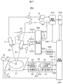
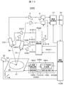
- FIG. 1 is a diagram illustrating a schematic configuration of an inspection apparatus 100 according to the first embodiment.
- the inspection apparatus in this embodiment includes a stage 31 on which a wafer 30 to be inspected is placed, a laser light source 32, image sensors 1 and 11, an apparatus control unit 20, a sensor control unit 22, an image processing unit 23, a GUI 24, and a processing unit. 28.
- a stage controller 60 is provided.
- the operator of the inspection apparatus has a GUI 24 (Graphical User Interface) or a user interface (not illustrated) connected to the apparatus control unit 20 (for example, an operation panel, a keyboard, a description file such as an inspection information / condition (recipe) (Also called) Reading etc.) to set or select inspection conditions.
- the apparatus control unit 20 sends commands to the laser (light source) 32, the stage control unit 60, and the sensor control unit 22 based on the set inspection conditions.
- the laser light source 32 outputs irradiation light (inspection light) 33 to the wafer 30 placed on the stage 31 in accordance with a command from the apparatus control unit 20 (laser conditions such as laser power and wavelength). Irradiation of the irradiation light 33 to the wafer 30 may be performed by adjusting a spot, light intensity, or the like by arranging a lens, a mirror, a filter, or the like (not shown) in the optical path or the periphery of the irradiation light 33. From the wafer 30 irradiated with the irradiation light 33, scattered light 34 and 35 corresponding to the pattern, defect, and foreign matter state formed on the wafer 30 are generated.
- a plurality of scattered lights are generated, but two cases are shown as an example. Further, a lens, a mirror, a filter, etc. (not shown) are arranged on or around the optical path of the scattered light 34 and 35, and the light receiving surface of the image sensors 1 and 11 (generally a light emitting surface on which photodiodes are arranged in an array). ) May be adjusted.
- the stage control unit 60 includes a signal generation unit 61, a control unit 62, a position detection unit 63, and a trigger generation unit 64.
- the signal generation unit 61 Based on the inspection condition command S20 from the apparatus control unit 20, the signal generation unit 61 generates a command S21 indicating the direction (X, Y, Z) in which the stage 31 is transported and a signal S10 that is a source of the speed.
- the control unit 62 drives the stage 31 based on the command / signal.
- the position detector 63 detects the speed fluctuation amount of the stage 31, and the trigger signal generator 64 corrects the signal S10 according to the signal from the position detector 63, and generates a trigger signal S11 synchronized with the stage speed fluctuation.
- the trigger signal S11 output from the stage control unit 60 is input to the processing unit 28.
- a trigger signal S111 is generated based on the input trigger signal S11 by a method described later, and is sent to the sensor control unit 22. input.
- the sensor control signal (the light reception time control signal S12 of the image sensors 1, 11 and the image sensors 1, 11).
- a control signal S13) for operating the A / D converter 4 and an A / D control signal S14 for operating the A / D converters 4 and 14 are generated.
- the sensor control signals S12 and S13 are input to the image sensors 1 and 11 via the driver circuits 2, 5, 12, and 15.
- the sensor control signals S12 and S13 are signals synchronized with the image sensors 1 and 11, and control operations such as charge transfer inside the image sensor. For example, vertical control signals and horizontal transfers (shift registers) Image sensors to be applied (for example, charge-coupled devices (CCD: Charged Coupled Device) and CMOS sensors such as time delay integration type (TDI), linear type (line type), etc.) All the control signals necessary for the operation of are shown.
- CCD Charged Coupled Device
- CMOS sensors such as time delay integration type (TDI), linear type (line type), etc.
- All the control signals necessary for the operation of are shown.
- These sensor control signals S12 and S13 can be easily (or applied) as to what kind of signal the worker (designer or manufacturer of the image sensor or designer of the image sensor application apparatus) has. (By CCD specification).
- the A / D control signal S14 is input to the A / D converters 4 and 14 via the driver 6.
- the A / D control signal S14 is a signal including a sampling clock, and may include a signal necessary for operating in accordance with the applied A / D converter specification.
- the image sensors 1 and 11 receive the scattered light 34 and 35 for a predetermined time according to S2 of the sensor control signal, and output an electric signal corresponding to the received charge amount.
- the output signals of the sensors 1 and 11 are converted into digital data by the A / D converters 4 and 14 via the detection circuits 3 and 13.
- the detection circuits 3 and 13 are amplifier circuits having a buffer or gain, and may be omitted depending on the device configuration.
- the A / D converters 4 and 14 may include a function of correlated double sampling (CDS: Correlated Double Sampling) generally used for detecting an output signal of the image sensor.
- CDS Correlated Double Sampling
- the above operation is performed by moving one or more of the stage 31, the image sensors 1 and 11, and the laser light source 32 (or irradiation light 33) in the X, Y, or Z direction, and the wafer 30 preset by the operator.
- the inspection region (a part or a plurality of regions of the wafer 30 or the entire surface) is inspected.
- the image processing unit 23 forms an image based on the detection signals output from the image sensors 1 and 11 thus obtained and digitized by the A / D converters 4 and 14 and displays them on the GUI 24, for example.
- the present invention is not limited to this, and any configuration that can irradiate the wafer 30 with the irradiation light 33 may be used.
- a configuration in which a plurality of 32 are arranged may be used, and the light source is not limited to the laser.
- the configuration example in which two image sensors 1 and 11 are arranged has been described, but any configuration in which a plurality of two or more image sensors are arranged may be used.
- the characteristic of the inspection apparatus in the present embodiment is that a processing unit 28 is provided between the trigger generation unit 64 and the sensor control unit 22.
- a processing unit 28 is provided between the trigger generation unit 64 and the sensor control unit 22.
- the present embodiment will be described with reference to FIGS.
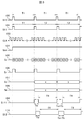
- the signal 101 (S11) in FIG. 3 shows the case where the error of the position of the stage 31 increases gradually as an example.
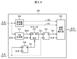
- FIG. 2 shows the configuration of the processing unit 28.
- the processing unit 28 includes an expected value generation unit 50, an EN generation unit 51, a counter 52, flip-flop circuit units 53 and 54, and an arithmetic / signal generation unit 55.
- the expected value generation unit 50 calculates an expected count value Sm (108 in FIG. 3) and an expected pulse width value St (omitted in FIG. 3) based on the inspection condition command S20 output from the apparatus control unit 20. Alternatively, the data is read from a table or memory (not shown) prepared in advance.
- the EN generation unit 51 outputs an enable signal Sen (104 in FIG. 3) indicating start or stop in synchronization with the clock signal CLK (103 in FIG. 3) based on the inspection condition instruction S20 output from the device control unit 20. .
- start is defined as “H”
- stop is defined as “L” level.
- the counter 52 counts the number of clocks of the clock signal CLK while the enable signal Sen is “H”, and outputs the count number Sc (105 in FIG. 3).
- the flip-flop circuit unit 53 latches (holds) the count number Sc output from the counter 52 at the rising edge of the trigger signal S11 (101 in FIG. 3) output from the trigger generation unit 64 of the stage control unit 60.
- the signal Sc ′ is output (107 in FIG. 3).
- the flip-flop circuit unit 54 synchronizes the trigger signal S11 (101 in FIG. 3) output from the trigger generation unit 64 with the rising edge of the clock signal CLK (103 in FIG. 3) and outputs it as a signal Sr (106 in FIG. 3). When the signal Sr is “H”, the counter value of the counter 52 is reset (cleared to zero).
- the arithmetic / signal generation unit 55 performs an operation from the signal Sc ′ output from the flip-flop circuit unit 53, the expected value Sm of the count number output from the expected value generation unit 50, and the expected value St of the pal width.
- a signal S111 is generated and output based on the result.
- the sensor control unit 22 uses the signal Sc ′ to output a sensor light reception time control signal S12 (109 in FIGS. 2 and 3) synchronized with the two images 1 and 11.
- the processing unit 28 (FIG. 2A) can be configured with relatively inexpensive components such as a logic circuit, a PDL (Programmable Logic Device), and a microcomputer.
- the calculation / signal generation unit 55 includes a calculation unit 551 and a signal generation unit 552 as shown in FIG. 2B.
- the computing unit 551 performs computation using the count value expectation value Sm and the signal Sc ′.
- the signal generator 552 generates and outputs a trigger signal S111.
- the “H” section and the “L” section of the trigger signal S111 generated by the signal generator 552 are determined by Expressions 1 and 2.
- “H” section of S111 St + (Sc′ ⁇ Sm) ⁇ clock signal period (Formula 1)
- “L” section of S111 Sm ⁇ clock signal period ⁇ (“H” section of S111) (Formula 2)
- the signal corresponding to the first period of the signal S11 (101) input from the apparatus control unit 20 to the processing unit 28 is the second period of the signal S11, and the signal corresponding to the second period is three periods. It is calculated by Equations 1 and 2 with a delay of one cycle.
- the count number Sc (105) also increases as X, Y, Z (X ⁇ Y ⁇ Z) with the period of the signal S11 (101).
- the signal corresponding to the second period of the signal S11 is calculated using Expression 1 and Expression 2, it is the “H” section of S111 (108) due to the difference between the count value Sc ′ and the expected value Sm.
- FIG. 2 shows an example of the configuration of the processing unit 28, and the present invention is not limited to this.
- the main point of the present embodiment is to adjust the time (pulse width) that becomes “H” in each cycle of the signal S11 and correct the time that becomes “L” to a set fixed time, which is realized. You may change into various structures.
- FIG. 4 shows a flow of processing for generating the trigger signal S111 in the present embodiment.
- inspection parameters are set from the GUI 24 or an input device (not shown) (Step 401).
- an inspection condition instruction S20 is sent from the apparatus control unit 20 to the stage control unit 60 based on the set parameters.
- an inspection condition command S20 is input, and a command S21 indicating the direction (X, Y, Z) for moving the stage 31 and a signal S10 related to the moving speed of the stage 31 are generated, and these are controlled by the control unit
- the stage 31 is controlled (Step 402).
- the position detection unit 63 detects the position of the stage 31 (Step 403) and sends the detection signal to the trigger signal generation unit 64.
- the trigger signal generation unit 64 generates a trigger signal S11 in response to the signal from the position detection unit 63 regarding the position of the stage 31 and the signal S10 generated by the signal generation unit 61 regarding the moving speed of the stage 31 (Step 404).
- the inspection condition instruction S20 output from the apparatus control unit 20 the trigger signal S11 output from the trigger signal generation unit 64 of the stage control unit 60, and the clock signal are input, and the expected value generation unit 50
- the count value expectation value Sm and the pulse width expectation value St are calculated and output to the calculation / signal generation unit 55 side.
- the EN generation unit 51 generates the enable signal Sen, and the counter 52 uses the count value Sc. Then, the signal Sc ′ output from the flip-flop circuit 53 is output to the arithmetic / signal generation unit 55 side (Step 405).
- the calculation unit 551 uses the expected count value Sm, the expected pulse width value St, and the signal Sc ′ to obtain a signal interval based on the formulas 1 and 2, and the signal generation unit 552
- the trigger signal S111 is generated (Step 406), and the generated trigger signal S111 is sent to the sensor control unit 22 together with the inspection condition command S20 (Step 407).
- Step 408 it is determined whether or not the inspection is completed. If the inspection is not completed (NO in Step 408), the process returns to Step 402 to execute Step 407 to generate the next trigger signal S111. When the inspection is completed (YES in Step 408), a series of investigations are ended.
- FIG. 10 illustrates a case where the processing unit 28 described in FIG. 1 is not provided as a comparative example of the present embodiment.
- the same components as those in the embodiment described in FIG. 1 are denoted by the same reference numerals, and the description thereof is omitted.
- the signal generation unit 1061 that configures the stage control unit 1060 is configured to convey the stage 31 based on the inspection condition instruction S1020 from the apparatus control unit 1020 (X, A command S1021 indicating Y, Z) and a signal S1010 which is a source of speed are generated, and the control unit 1062 controls the stage 31 based on the command / signal.
- the position detection unit 1063 detects the speed fluctuation amount of the stage 31, the trigger signal generation unit 1064 corrects the signal S1010 according to the signal from the position detection unit 1063, and generates a trigger signal S1011 synchronized with the stage speed fluctuation.
- sensor control signals (light reception time control signal S1012 of the image sensors 1001 and 1011, control signal S1013 for operating the image sensor), An A / D control signal S1014 for operating the A / D converters 4 and 14 is generated.
- the sensor control signals S1012 and S1013 are input to the image sensors 1001 and 1011 via the driver circuits 1002, 1005, 1012 and 1015.
- the signal 1100 (S1010) is an output signal of the signal generation unit 1061, and is a trigger signal generated based on the inspection condition command S1020 and having a constant period T1.
- the period T1 is determined by the signal generation unit 1061 according to the pattern structure of the wafer, the inspection area, and the like.
- a signal 1101 (S1011) is an output signal of the trigger signal generation unit 1064 and is obtained by correcting the signal 1100 (S1010) with stage error information.
- FIG. 11 shows a case where the stage error gradually increases as an example, and the period gradually increases as T1, T2, T3 (T1 ⁇ T2 ⁇ T3).
- a signal 1102 (S1012) is a light reception time control signal for the image sensors 1001 and 1011.
- the sensor control unit 1022 converts the pulse width of the signal 1101 (S1011) into Ta.
- the width (time) of Ta is determined according to the inspection condition instruction S1020 and the applied image sensor specifications.
- the time delay between the signal 1101 (S1011) and the signal 1102 (S1012) indicates the processing time of the sensor control unit 1022.
- the time Ta corresponds to the vertical transfer of the image sensors 1001 and 1011 and the times T1 ′, T2 ′ and T3 ′ (T1 ′ ⁇ T2 ′ ⁇ T3 ′) correspond to the light reception times of the image sensors 1001 and 1011. To do.
- the light reception time of the image sensor changes as the stage position error gradually increases.
- the amount of sensor output signal changes in proportion to the light reception time. Therefore, in the inspection apparatus 1000 that does not include the processing unit 28. Even if the wafers having the same pattern are inspected, the brightness of the image varies.
- the light reception time is constant when the processing unit 28 controls the sensor control unit 22 to synchronize the sensors 1 and 11. Therefore, it is possible to suppress fluctuations in brightness of an image obtained by detection, and to realize a more accurate inspection.
- FIG. 5A is a diagram showing a configuration of a processing unit 228 that replaces the processing unit 28 of the inspection apparatus (FIG. 1) described in the first embodiment as a second embodiment of the present invention.
- the difference from the processing unit 28 of the first embodiment is a method for correcting the input signal S11 to the output signal S211 in the processing unit 228 of the present embodiment.
- FIGS. 5A, 5B, and 6. FIG. Note that the signal 101 (S11) in FIG. 6 is the same as S10 and S11 described in the first embodiment, and shows an example in which the error in the position of the stage 31 gradually increases.
- the processing unit 228 shown in FIG. 5A in this embodiment includes an expected value generation unit 70, an EN generation unit 71, a counter 72, and an arithmetic / signal generation unit 73.
- the expected value generation unit 70 calculates the expected count value Sm2 (122 in FIG. 6) and the expected pulse width value St2 (omitted in FIG. 6) based on the inspection condition command S20 output from the apparatus control unit 20. Alternatively, the data is read from a table or memory (not shown) prepared in advance.
- the EN generation unit 71 is based on the check condition command S20 and the periodic operation of the signal S11 output from the signal generation unit 61, and an enable signal Sen2 (FIG. 6) indicating start or stop synchronized with the clock signal CLK (103 in FIG. 6). 120) is output. In this embodiment, start is defined as “H” and stop is defined as “L” level.
- the counter 72 counts the number of clocks of the clock signal CLK while the enable signal Sen2 is “H”, and outputs a count number signal Sc2 (121 in FIG. 6).
- the calculation / signal generation unit 73 performs a comparison operation between the count signal Sc2 and the expected count value Sm2, generates a signal S211 based on the result, and outputs the signal S211 to the sensor control unit 22 (see FIG. 1).
- the signal Sr2 (123 in FIG. 6) which synchronizes the signal S11 with the rising edge of the clock signal CLK is output “H”, and the count value of the counter 72 is reset ( Zero clear).
- the sensor control unit 22 (FIG. 1) uses the signal Sc2 and outputs a light reception time control signal S22 (125 in FIG. 5) of the image sensor synchronized with the two images 1 and 11.
- the processing unit 228 (FIG. 5) can be configured by relatively inexpensive components such as a logic circuit, a PLD (Programmable Logic Device), and a microcomputer.
- FIG. 5B shows the configuration of the calculation / signal generation unit 73.
- the calculation / signal generation unit 73 includes a calculation unit 731, a signal generation unit 732, and a comparison unit 733.
- the calculation unit 731 calculates using the count value expectation value Sm2 that is a signal input from the expected value generation unit 70 and the count number signal Sc2 that is a signal input from the counter 72, and generates a signal based on the calculation result.
- the unit 732 generates a trigger signal S211 and outputs it to the sensor control unit 22 (see FIG. 1).
- the “H” section and the period of the trigger signal S211 are determined by Expressions 3 and 4.
- “H” section of S211 St2 (Formula 3)
- S211 cycle Sm2 x clock signal cycle (Formula 4)
- the pulse width is fixed at the expected value Ta, and the comparison unit 733 compares the count number Sc2 with the expected count value Sm2, and the count number Sc2 (121) becomes the expected count value Sm2. Since S211 transitions to "H” when they are the same, it can be made constant at T5, equivalent to the entire period.
- the processing in the image processing unit 23 is facilitated. Furthermore, since the pulse width of the signal S211, that is, the vertical transfer time of the image sensor can be fixed, channel variations such as an image lag (charge transfer residual) characteristic error of the image sensor can be reduced as compared with the first embodiment.
- 5A and 5B show an example of the configuration of the processing unit 228, and the present invention is not limited to this.
- the main point of the present embodiment is that the time (pulse width) that becomes “H” in each cycle of the signal S11 is made constant according to the inspection, and is corrected to a constant time by fixing it to the expected count value Sm2.
- the configuration may be changed to various configurations that realize this.
- the parameters are the specification range of the image sensor to be applied by the worker who develops the inspection device. Should be set in view of the above.
- the frequency of the clock signal CLK (104) may be determined from the specifications of the image sensor to be applied and the step time for adjusting the pulse width of the signal S1 '. For example, 50 MHz or 500 MHz is applied.
- the clock signal CLK may be configured to switch between clock signals having a plurality of frequencies.
- FIG. 7 A third embodiment of the present invention will be described with reference to FIGS. 7, 8A, 8B and 9.
- FIG. 7 In the inspection apparatus 700 according to the present embodiment shown in FIG. 7, the same components as those in the inspection apparatus 100 according to the first embodiment described with reference to FIG. 7, the trigger signal S11 generated by the trigger signal generation unit 64 of the stage control unit 60 is input to the device control unit 320, and the processing unit 328 outputs the trigger signal S11 from the device control unit 320. 1 is different from the configuration of the inspection apparatus 100 shown in FIG. 1 described in the first embodiment in that the trigger signal S311 is generated and output to the sensor control unit 322 using the inspection condition instruction S20.
- the sensor control unit 322 Upon receiving the trigger signal S311 from the processing unit 328, the sensor control unit 322 receives the sensor control signal (the light reception time control signal S312 of the image sensors 1 and 11, the control signal S313 for operating other sensors), and the A / D An A / D control signal S314 for operating the converters 4 and 14 is generated.
- the trigger signal S11 reflecting the speed variation error information of the stage 31 generated by the trigger signal generation unit 64 is input to the device control unit 320, and the device control unit 320 inputs the trigger signal.
- an image shift correction signal S321 is generated and output to the image processing unit 323.
- the image processing unit 323 generates an image based on each image sensor output signal while correcting the positional shift of the signals output from the image sensors 1 and 11 based on the image shift correction signal S321. As a result, it is possible to obtain a more accurate image that is not affected by the fluctuation error in the speed of the stage 31.
- FIG. 8A shows the configuration of the processing unit 328.
- the processing unit 328 includes an EN generation unit 351, a counter 352, an inspection rate setting unit 353, and an arithmetic / signal generation unit 355.
- the EN generation unit 35 based on the inspection condition instruction S20 output from the device control unit 320, enables an enable signal Sen3 (904 in FIG. 9) and a pulse width indicating start or stop synchronized with the clock signal CLK (903 in FIG. 9).
- An expected value St3 (omitted in FIG. 9) is output.
- start is defined as “H”
- stop is defined as “L” level.
- the counter 352 counts the number of clocks of the clock signal CLK while the enable signal Sen3 is “H”, and outputs the count number Sc3 (905 in FIG. 9) to the arithmetic / signal generation unit 355.
- the inspection rate setting unit 353 receives the inspection condition command S20, creates an inspection rate signal Si3 (906 in FIG. 9), and outputs the inspection rate signal Si3 to the calculation / signal generation unit 355.
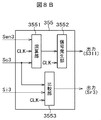
- the configuration of the calculation / signal generation unit 355 is shown in FIG. 8B.
- the calculation / signal generation unit 355 includes a calculation unit 3551, a signal generation unit 3552, and a comparison unit 3553.
- the calculation unit 3551 receives the enable signal Sen3 generated by the EN generation unit 351, the signal related to the count number Sc3 output from the counter 352, and the clock signal CLK, performs calculation, and outputs the result to the signal generation unit 3552.
- the signal generation unit 3552 receives the signal from the calculation unit 3551, generates a trigger signal S 311, and outputs the trigger signal S 311 to the sensor control unit 322.
- the trigger signal S311 “H” section and “L” section generated by the signal generator 3552 are determined by Expressions 5 and 6.
- the comparison unit 3553 compares the count number Sc3 output from the counter 352 with the inspection rate setting value Si3 output from the inspection rate setting unit 353, and resets when the count number Sc3 and the inspection rate setting value Si3 become the same.
- the signal Sr3 is output and input to the reset signal input terminal of the counter 352, and the count number Sc3 is reset to zero.
- the feature of this embodiment is that the sensor control and the stage control are separated and controlled, and the image processing unit is configured to correct the error due to the stage control. Therefore, it is suitable for a linear image sensor application apparatus suitable for independent control. By adopting this configuration, it is possible to easily reduce the brightness variation of the image generated by the output signals from the image sensors 1 and 11 to an extent that does not affect the inspection, as compared with the other embodiments.
- Embodiments 1 to 3 can solve the problem by disposing a processing unit in a conventional inspection apparatus, it can be compatible with the conventional inspection apparatus. For this reason, the performance of the apparatus can be improved by replacing the circuits and functions of the conventional inspection apparatus. As a result, the semiconductor manufacturer can obtain an effect of suppressing the capital investment.
- Embodiments The present invention is not limited to the above-described embodiments, and includes various modifications.
- the above-described embodiments have been described in detail for easy understanding of the present invention, and are not necessarily limited to those having all the configurations described.
- a part of the configuration of one embodiment can be replaced with the configuration of another embodiment, and the configuration of another embodiment can be added to the configuration of one embodiment.
- Each of the above-described configurations, functions, processing units, processing means, and the like may be realized by hardware by designing a part or all of them with, for example, an integrated circuit.
- Each of the above-described configurations, functions, and the like may be realized by software by interpreting and executing a program that realizes each function by the processor.
- Information such as programs, tables, and files for realizing each function can be stored in a recording device such as a memory, a hard disk, an SSD (Solid State Drive), or a recording medium such as an IC card, an SD card, or a DVD.
- a recording device such as a memory, a hard disk, an SSD (Solid State Drive), or a recording medium such as an IC card, an SD card, or a DVD.
- the operation / effect of the present invention is described in an easy-to-understand manner.
- the case where the stage gradually increases has been described.
- the present invention is not limited to the increase in the stage, and the stage varies. Needless to say, all of the above-described embodiments can be applied to the inspection apparatus, and the problem can be solved and the effect thereof can be realized.
Landscapes
- Physics & Mathematics (AREA)
- Health & Medical Sciences (AREA)
- Life Sciences & Earth Sciences (AREA)
- Chemical & Material Sciences (AREA)
- Analytical Chemistry (AREA)
- Biochemistry (AREA)
- General Health & Medical Sciences (AREA)
- General Physics & Mathematics (AREA)
- Immunology (AREA)
- Pathology (AREA)
- Investigating Materials By The Use Of Optical Means Adapted For Particular Applications (AREA)
Abstract
複雑かつ微小サイズのパターン・欠陥の検査に好適な検査装置とその制御方法を提供するために、移動しているステージに載置された試料に光源部から発射した光を照射し、光が照射された試料からの散乱光を検出するタイミングを制御しながらイメージセンサで検出し、試料からの散乱光を検出したイメージセンサからの出力信号を画像処理部で受けてこの画像処理部で受けた出力信号から試料パターンの画像を生成してこの生成した画像から試料パターンの欠陥を検出し、画像処理部で処理した結果を画面上に表示する検査装置および欠陥検査方法において、イメージセンサの受光時間を一定にするトリガ信号を生成し、生成したトリガ信号を用いてイメージセンサの受光時間が一定になるように制御して試料からの散乱光を検出するようにした。
Description
本発明は、半導体ウェハ、半導体装置(半導体集積回路装置)、フォトマスク(露光マスク)、液晶パネルなどの欠陥を検査、計測、または観察を行う検査装置及び検査方法に関する。
本発明に関連する半導体検査装置として、特開2010-91552号公報(特許文献1)がある。この公報では、光源を検査対象に照射して、イメージセンサで検出する光学式の検査システム(検査装置)の構成や検査方法の概要が記載されている(特許文献1〔背景技術〕参照)。特許文献1では、フォトマスクを検査対象として記載されているがフォトマスク検査に限定された装置構成ではなく、例えば半導体ウェハを対象とした検査装置(半導体検査装置)では、一例として特許文献1の段落[006]に記載のように、イメージセンサとステージとを同期させる装置構成を有することがある。
ウェハなどの検査対象物を搬送するステージは、機械部品を主たる構成に用いているため、常に一定速度で動作させることが難しく、速度変動が生じてしまう。このような状態で、ステージの移動速度とイメージセンサの検出タイミングとを同期化させた検査装置では、ステージの速度変動に合わせてイメージセンサが光を検出している時間、即ち受光時間(露光時間、撮像時間ともいう)が制御されるため、同一パターンのウェハを検査しても、ステージの測度変動に伴うイメージセンサの受光時間の変動により、同一の明度画像が得られないという課題がある。
更に、近年の微細化技術による複雑かつ微小パターンや欠陥に、光源(例えば、連続発振やパルス発振のレーザ光など)用いて光照射した場合、ウェハからの散乱光も従来以上に微弱なもとなってきているため、ステージ速度変動に伴う画像の明度変動により、検査感度や欠陥検出率が低下して、市場での不良率増加を招いてしまう課題がある。
この課題を解決するため、特許文献1記載のセンサ出力値を補正する技術を応用して、ステージ速度変動分をセンサ出力値に補正する手段を設けた場合、センサ出力に重畳したノイズ成分(例えば、センサ内で発生するショットノイズやセンサ出力回路ノイズなど)も増幅されるため、ステージ変動に応じてノイズ量が変動した画像で検査することになる。このため、同一パターンのウェハを検査してもノイズ成分の異なった画像となり、その結果、特に複雑かつ微小パターン検査では、検査感度や欠陥検出率が低下する課題がある。
本発明は、上記課題を解決して、複雑かつ微小サイズのパターン・欠陥の検査に好適な検査装置及び検査方法を提供するものである。
本願において開示される発明のうち、代表的なものの概要を簡単に説明すれば、次の通りである。
即ち、本発明は、検査装置を、検査対象である試料を載置して移動可能なステージ部と、ステージ部に載置された試料に光を照射する光源部と、光源部からの光が照射された試料からの散乱光を検出するイメージセンサを備えた検出部と、検出部のイメージセンサによる散乱光の検出を制御するセンサ制御部と、試料からの散乱光を検出した検出部からの出力信号を受けて試料パターンの画像を生成してこの生成した画像から試料パターンの欠陥を検出する画像処理部と、画像処理部で処理した結果を表示する表示部と、ステージ部を駆動すると共にステージの位置を検出する位置検出部と位置検出部で検出したステージの位置情報に基づいてトリガ信号を生成するトリガ信号生成部とを有するステージ制御部と、光源部と検出部と画像処理部と表示部とステージ制御部とセンサ制御部とを制御する装置制御部と、ステージ制御部のトリガ信号発生部で生成した信号と装置制御部からステージ制御部に出力した信号とを受けてセンサ制御部で検出部のイメージセンサによる検出を制御するトリガ信号を生成する処理部とを備えて構成した。
また、本発明は、検査装置を、検査対象である試料を載置して移動可能なステージ部と、ステージ部に載置された試料に光を照射する光源部と、光源部からの光が照射された試料からの散乱光を検出するイメージセンサを備えた検出部と、検出部のイメージセンサによる散乱光の検出を制御するセンサ制御部と、試料からの散乱光を検出した検出部からの出力信号を受けて試料パターンの画像を生成してこの生成した画像から試料パターンの欠陥を検出する画像処理部と、画像処理部で処理した結果を表示する表示部と、ステージ部を駆動すると共にステージの位置を検出する位置検出部とこの位置検出部で検出したステージの位置情報に基づいてトリガ信号を生成するトリガ信号生成部とを有するステージ制御部と、光源部と検出部と画像処理部と表示部とステージ制御部とセンサ制御部とを制御する装置制御部と、装置制御部からステージ制御部に出力した信号を受けてセンサ制御部で検出部のイメージセンサによる検出を制御するトリガ信号を生成する処理部とを備えて構成した。
更に、本発明では、移動しているステージに載置された試料に光源部から発射した光を照射し、光が照射された試料からの散乱光を検出するタイミングを制御しながらイメージセンサで検出し、試料からの散乱光を検出したイメージセンサからの出力信号を画像処理部で受けてこの画像処理部で受けた出力信号から試料パターンの画像を生成してこの生成した画像から試料パターンの欠陥を検出し、画像処理部で処理した結果を画面上に表示する欠陥検査方法において、イメージセンサの受光時間を一定にするトリガ信号を生成し、生成したトリガ信号を用いてイメージセンサの受光時間が一定になるように制御して試料からの散乱光を検出するようにした。
本願において開示される発明のうち、代表的なものによって得られる効果を簡単に説明すれば以下の通りである。
本発明の代表的な実施の形態によれば、第一に、特に複雑かつ微小サイズのパターン・欠陥を対象とした検査装置の検査感度を向上し、市場での不良率を抑制することができる。第二に、それらを安価な手段、かつ従来の検査装置との互換回路手段によって実現することで、半導体製造メーカ等の投資を抑制できる。
本発明は、検査装置において、イメージセンサの受光時間を一定にするトリガ信号を生成し、生成したトリガ信号を用いて、2つ以上の複数配置されたイメージセンサの受光時間が一定になるように同期制御して試料からの散乱光を検出するようにして検査感度を向上させ、より微細な欠陥を高感度に検出できるようにしたものである。
以下、具体的に本発明の実施例を添付図面に従って説明する。なお、本発明の実施例を説明するための全図において、同一の機能を有する部材には原則として同一の符号を付し、その繰り返しの説明は省略する。また、各実施例における検査装置の基本動作は、上述した従来の検査装置と同様なため省略し、各実施例に関わる動作とその要点に限定して説明する。
図1は、第1の実施例における検査装置100の概略構成を示す図である。
本実施例における検査装置は、検査対象であるウェハ30を載置するステージ31、レーザ光源32、イメージセンサ1及び11、装置制御部20、センサ制御部22、画像処理部23、GUI24、処理部28、ステージ制御部60を備えている。
本実施例における検査装置は、検査対象であるウェハ30を載置するステージ31、レーザ光源32、イメージセンサ1及び11、装置制御部20、センサ制御部22、画像処理部23、GUI24、処理部28、ステージ制御部60を備えている。
上記構成において、検査装置の操作者は、GUI24(Graphical User Interface)や、装置制御部20と接続する図示を省略したユーザーインターフェース(例えば、操作パネル、キーボード、検査情報・条件等の記載ファイル(レシピとも呼ぶ)読み込みなど)から検査条件などが設定または選択させる。装置制御部20では、設定された検査条件にもとづき、レーザ(光源)32、ステージ制御部60、センサ制御部22へ命令を送る。
レーザ光源32では、装置制御部20からの命令(レーザーパワー、波長などのレーザ条件)に応じて、ステージ31に配置したウェハ30へ照射光(検査光)33を出力する。ウェハ30への照射光33の照射は、図示しないレンズ、ミラー、フィルタ等を照射光33の光路または周囲に配置して、スポットや光強度などを調整してもよい。照射光33が照射されたウェハ30からは、ウェハ30に形成されたパターン、欠陥、異物状況に応じた散乱光34、35が発生する。実際には複数の散乱光が発生するが、一例として2つの場合を示す。また、図示しないレンズ、ミラー、フィルタ等を散乱光34、35の光路またはその周囲に配置して、イメージセンサ1、11の受光面(一般的にフォトダイオードがアレイ状に配置された光照射面)へ集光するなど調整してもよい。
ステージ制御部60は、信号生成部61、制御部62、位置検出部63、トリガ生成部64を備えている。信号生成部61では、装置制御部20からの検査条件命令S20にもとづき、ステージ31を搬送させる向き(X,Y,Z)を示す命令S21と、速度の元となる信号S10を生成し、この命令・信号をもとに制御部62がステージ31を駆動する。位置検出部63はステージ31の速度変動量を検出し、トリガ信号生成部64で位置検出部63からの信号に応じて信号S10を補正し、ステージ速度変動に同期したトリガ信号S11を生成する。
ステージ制御部60から出力されたトリガ信号S11は,処理部28に入力し、処理部28においてこの入力したトリガ信号S11に基づいて後述する方法でトリガ信号S111が生成されて、センサ制御部22に入力する。
センサ制御部22では、装置制御部20からの命令S20と、処理部28から出力されたトリガ信号S111にもとづき、センサ制御信号(イメージセンサ1,11の受光時間制御信号S12、イメージセンサ1,11を動作させるための制御信号S13)と、A/Dコンバータ4,14を動作させるためのA/D制御信号S14とを生成する。センサ制御信号S12,S13は、ドライバ回路2,5,12,15を介して、イメージセンサ1,11に入力される。
センサ制御信号S12,S13とは、イメージセンサ1,11とで同期がとれた信号であり、イメージセンサ内部の電荷転送などの動作を制御するもので、例えば、垂直転送信号、水平転送(シフトレジスタ転送)信号などであり、適用するイメージセンサ(例えば、時間遅延積分型(TDI:Time Delay Integration)型、リニア型(ライン型)などの電荷結合素子(CCD:Charge Coupled Device)やCMOSセンサなど)の動作に必要な全ての制御信号を示す。このセンサ制御信号S12,S13は、当該従事者(イメージセンサの設計者やメーカ、イメージセンサ適用装置の設計者など)であれば、どのような信号種であるかは、容易に(または適用するCCDの仕様にて)把握することができるであろう。
A/D制御信号S14は、ドライバ6を介して、A/Dコンバータ4,14に入力される。A/D制御信号S14とは、サンプリングクロックを含む信号であり、適用するA/Dコンバータ仕様に合わせて動作させるに必要な信号を含む構成であっても良い。
イメージセンサ1,11は、センサ制御信号のS2に応じて一定時間、散乱光34,35を受光し、受光した電荷量に相当する電気信号を出力する。センサ1,11の出力信号は、検出回路3,13を介してA/Dコンバータ4,14にてデジタルデータに変換される。検出回路3,13はバッファまたはゲインを有したアンプ回路であり、装置構成によっては省略してもよい。A/Dコンバータ4,14は、一般にイメージセンサの出力信号を検出するに用いられる相関二重サンプリング(CDS:Correlated Double Sampling)の機能を含むものであってもよい。
以上の動作を、ステージ31、イメージセンサ1,11、レーザ光源32(または照射光33)のうち1つまたは複数をX、YまたはZの方向に移動させて、操作者が予め設定したウェハ30の検査領域(ウェハ30の一部または複数領域、或いは全面)を検査する。
画像処理部23では、このようにして得られたイメージセンサ1,11から出力されてA/Dコンバータ4,14でデジタル化した検出信号をもとに画像化し、例えばGUI24などに表示する。
なお、レーザ光源32は、ウェハ30に対して、斜めに配置するように図示したが、これに限定されるものではなく、ウェハ30へ照射光33を照射できる構成であれば構わず、レーザ光源32が複数配置される構成であっても良く、光源はレーザに限定されるものではない。また、イメージセンサ1と11の2つ配置する構成例を示したが、2つ以上のイメージセンサが複数配置された構成であれば構わない。
本実施例における検査装置の特徴は、トリガ生成部64とセンサ制御部22との間に処理部28を設けた点である。以下、図2,図3を用いて本実施例について説明する。なお、図3における信号101(S11)は、一例としてステージ31の位置の誤差が徐々に増加した場合を示す。
図2は、処理部28の構成を示す。処理部28は、期待値生成部50、EN生成部51、カウンタ52、フリップフロップ回路部53、54及び演算・信号発生部55を備えている。
期待値生成部50は、装置制御部20から出力された検査条件命令S20にもとづき、カウント数の期待値Sm(図3の108)とパルス幅の期待値St(図3では省略)とを演算、または予め用意されたテーブルやメモリなど(図示せず)から読み出す。
EN生成部51は、装置制御部20から出力された検査条件命令S20にもとづき、クロック信号CLK(図3の103)に同期した開始または停止を示すイネーブル信号Sen(図3の104)を出力する。本実施例では開始を“H”、停止を“L”レベルと定義する。カウンタ52では、イネーブル信号Senが“H”の期間、クロック信号CLKのクロック数をカウントし、カウント数Sc(図3の105)を出力する。
フリップフロップ回路部53では、カウンタ52から出力されたカウント数Scを、ステージ制御部60のトリガ生成部64から出力されたトリガ信号S11(図3の101)の立上がりでラッチ(保持)して、信号Sc’として出力する(図3の107)。フリップフロップ回路部54は、トリガ生成部64から出力されたトリガ信号S11(図3の101)をクロック信号CLK(図3の103)の立上がりで同期化さて信号Sr(図3の106)として出力し、信号Srが“H”によって、カウンタ52のカウンタ値がリセット(ゼロクリア)させる。
演算・信号発生部55では、フリップフロップ回路部53から出力された信号Sc’と、期待値生成部50から出力されたカウント数の期待値Sm、パル幅の期待値Stから演算を行い、この結果をもとに信号S111を生成して出力する。
センサ制御部22(図1)では、信号Sc’を用い、2つのイメージ1,11とで同期したセンサの受光時間制御信号S12(図2,図3の109)を出力する。処理部28(図2A)は、例えばロジック回路やPDL(Programmable Logic Device),マイコンなどの比較的安価な部品で構成できる。
次に演算・信号発生部55の構成とその動作について説明する。演算・信号発生部55は、図2Bに示すように、演算部551と信号発生部552を備えている。演算部551では、カウント数の期待値Smと信号Sc’とを用いて演算する。信号発生部552では、トリガ信号S111を生成して出力する。信号発生部552で生成するトリガ信号S111の“H”区間と“L”区間は、式1,式2により決められる。
S111の“H”区間=St+(Sc’-Sm)×クロック信号周期 (式1)
S111の“L”区間=Sm×クロック信号周期-(S111の“H”区間) (式2)
S111の“H”区間=St+(Sc’-Sm)×クロック信号周期 (式1)
S111の“L”区間=Sm×クロック信号周期-(S111の“H”区間) (式2)
図3のように、装置制御部20から処理部28に入力する信号S11(101)の1周期目に相当する信号は、信号S11の2周期目に、2周期目に相当する信号は3周期目にと、1周期遅れて式1,式2により演算される。ここで、パル幅の期待値St=Taとすると、信号S11の1周期目に相当する信号では、Sc’=Sm=xであり、式1によりS111の“H”区間=Ta、S10の“L”区間=x×クロック信号周期-Ta(=T4と定義する)となる。
図3の例では、ステージ31の位置の誤差が徐々に増加するため、カウント数Sc(105)も信号S11(101)周期と共にX,Y,Z(X<Y<Z)と増加する。上記と同様に、信号S11の2周期目に相当する信号を式1,式2を用いて計算すると、カウント値Sc’と期待値Smとの差分によりS111(108)の“H”区間であるパルス幅が変動(Ta+Tb、Tb=y-x)し、S111の“L”区間は、全周期と同等にT4と一定にすることができる。即ち、ステージ31の位置の誤差の変動に応じて、信号S1(101)の周期がT1,T2,T3と変動しても、イメージセンサの受光時間に相当するT4の時間を一定に補正することで、画像の明度変動の課題を解決することができる。
図2は、処理部28の構成一例を示したものであり、これに限定されるものではない。本実施例の要点は、信号S11の各周期で“H”となる時間(パルス幅)を調整し、“L”となる時間を設定された一定時間に補正するというものであり、これ実現する各種構成に変更しても良い。
図4に、本実施例におけるトリガ信号S111を生成する処理の流れを示す。
まず、GUI24又は図示していない入力装置から、検査パラメータを設定する(Step401)。次に、この設定されたパラメータに基づいて装置制御部20からステージ制御部60に検査条件命令S20を送る。ステージ制御部60では、検査条件命令S20を入力して、ステージ31を移動させる向き(X,Y,Z)を示す命令S21と、ステージ31の移動速度に関する信号S10を作成し、それらを制御部62へ送り、ステージ31を制御する(Step402)。
まず、GUI24又は図示していない入力装置から、検査パラメータを設定する(Step401)。次に、この設定されたパラメータに基づいて装置制御部20からステージ制御部60に検査条件命令S20を送る。ステージ制御部60では、検査条件命令S20を入力して、ステージ31を移動させる向き(X,Y,Z)を示す命令S21と、ステージ31の移動速度に関する信号S10を作成し、それらを制御部62へ送り、ステージ31を制御する(Step402)。
制御部62からの信号でステージ31が駆動されると、位置検出部63でステージ31の位置を検出して(Step403)、その検出信号をトリガ信号生成部64へ送る。トリガ信号生成部64では、ステージ31の位置に関する位置検出部63からの信号とステージ31の移動速度に関する信号生成部61で生成した信号S10とを受けてトリガ信号S11を生成する(Step404)。
処理部28では、装置制御部20から出力された検査条件命令S20とステージ制御部60のトリガ信号生成部64から出力されたトリガ信号S11とクロック信号とを入力して、期待値生成部50でカウント数の期待値Smとパルス幅の期待値Stを算出し、演算・信号発生部55の側に出力するとともに、EN生成部51でイネーブル信号Senを作成してカウンタ52でカウント数Scに基づいてフリップフロップ回路53から出力された信号Sc’を演算・信号発生部55の側に出力する(Step405)。
演算・信号発生部55では、演算部551でカウント数の期待値Smとパルス幅の期待値St及び信号Sc’を用いて式1及び式2に基づいて信号区間を求め、信号発生部552でトリガ信号S111を生成し(Step406)、この生成されたトリガ信号S111は、検査条件命令S20と共にセンサ制御部22へ送られる(Step407)。
次に、検査が終了したかを判定し(Step408)、終了していない場合には(Step408でNOの場合)、Step402へ戻ってStep407までを実行して次のトリガ信号S111を生成する。検査が終了した場合には(Step408でYESの場合)、一連の捜査を終了する。
図10に本実施例の比較例として、図1で説明した処理部28を備えない場合について説明する。図10において、図1で説明した本実施例における装置構成と同じ構成については同じ番号を付して、その説明を省略する。
図10に示した比較例の検査装置1000の構成において、ステージ制御部1060を構成する信号生成部1061では、装置制御部1020からの検査条件命令S1020にもとづき、ステージ31を搬送させる向き(X,Y,Z)を示す命令S1021と、速度の元となる信号S1010を生成し、この命令・信号をもとに制御部1062がステージ31を制御する。位置検出部1063はステージ31の速度変動量を検出し、トリガ信号生成部1064で位置検出部1063からの信号に応じて信号S1010を補正し、ステージ速度変動に同期したトリガ信号S1011を生成する。
センサ制御部1022では、装置制御部1020からの命令S1020と、トリガ信号S1011にもとづき、センサ制御信号(イメージセンサ1001,1011の受光時間制御信号S1012、イメージセンサ動作させるための制御信号S1013)と、A/Dコンバータ4,14を動作させるためのA/D制御信号S1014とを生成する。センサ制御信号S1012,S1013は、ドライバ回路1002,1005,1012,1015を介して、イメージセンサ1001,1011に入力される。
次に、イメージセンサ1001,1011の受光時間と制御信号の関係について、図10と図11を参照して動作概要を説明する。なお、符号が1100番台は図11を、その他は図10を参照するものとする。
信号1100(S1010)は、信号生成部1061の出力信号で、検査条件命令S1020にもとづき生成され一定周期T1のトリガ信号である。周期T1は、ウェハのパターン構造や検査領域などに応じて信号生成部1061で決められる。信号1101(S1011)は、トリガ信号生成部1064の出力信号で、信号1100(S1010)をステージ誤差情報で補正したものである。
図11では、一例としてステージ誤差が徐々に増加した場合を示しており、周期がT1,T2,T3(T1<T2<T3)と徐々に増加している。信号1102(S1012)は、イメージセンサ1001,1011の受光時間制御信号であり、センサ制御部1022で信号1101(S1011)のパルス幅をTaに変換生成する。Taの幅(時間)は、検査条件命令S1020と適用するイメージセンサ仕様に応じて決定される。信号1101(S1011)と信号1102(S1012)との時間遅れは、センサ制御部1022の処理時間分を示す。信号1102(S1012)において、時間Taはイメージセンサ1001,1011の垂直転送、時間T1’,T2’,T3’(T1’<T2’<T3’)は、イメージセンサ1001,1011の受光時間に相当する。
このように、本実施例の比較例として説明した図10に示したような処理部28を備えていない検査装置1000では、ステージの位置の誤差が徐々に増加すると、イメージセンサの受光時間が変化する。一般に、イメージセンサ1001,1011は、同一の光強度で同一の光スポット径であった場合、受光時間に比例してセンサ出力信号量が変化するため、処理部28を備えていない検査装置1000では、同一パターンのウェハを検査しても画像の明度変動が生じてしまう。
これに対して図1乃至図4を用いて説明した本実施例による検査装置100では、処理部28でセンサ制御部22を制御してセンサ1及び11とを同期化させての受光時間が一定になるようにしたので、検出して得られる画像の明度変動を抑えることができ、より高精度な検査を実現できる。
図5Aは、本発明の第2の実施例として、実施例1で説明した検査装置(図1)の処理部28と置き換える処理部228の構成を示す図である。実施例1の処理部28との差異は、本実施例の処理部228における入力信号S11を出力信号S211への補正方法である。以下、図5A,図5B,図6を用いて本実施例について説明する。なお、図6における信号101(S11)は、実施例1で説明したS10,S11と同一であり、一例としてステージ31の位置の誤差が徐々に増加した場合を示す。
本実施例における図5Aに示した処理部228は、期待値生成部70、EN生成部71、カウンタ72、演算・信号発生部73を備えている。
期待値生成部70は、装置制御部20から出力される検査条件命令S20にもとづき、カウント数の期待値Sm2(図6の122)とパルス幅の期待値St2(図6では省略)とを演算、または予め用意されたテーブルやメモリなど(図示せず)から読み出す。EN生成部71は、検査条件命令S20と信号生成部61から出力される信号S11の周期動作にもとづき、クロック信号CLK(図6の103)に同期した開始または停止を示すイネーブル信号Sen2(図6の120)を出力する。本実施例では開始を“H”、停止を“L”レベルと定義する。カウンタ72では、イネーブル信号Sen2が“H”の期間、クロック信号CLKのクロック数をカウントし、カウント数信号Sc2(図6の121)を出力する。
演算・信号発生部73では、カウント数信号Sc2と、カウント数の期待値Sm2の比較演算を行い、この結果をもとに信号S211を生成してセンサ制御部22(図1参照)へ出力するとともに、カウンタ値Sc2とカウンタ期待値Sm2とが一致すると、信号S11をクロック信号CLKの立ち上がりと同期させた信号Sr2(図6の123)が“H”出力し、カウンタ72のカウント値をリセット(ゼロクリア)する。センサ制御部22(図1)では、信号Sc2を用い、2つのイメージ1,11とで同期したイメージセンサの受光時間制御信号S22(図5の125)を出力する。処理部228(図5)は、例えばロジック回路やPLD(Programmable Logic Device),マイコンなどの比較的安価な部品で構成できる。
図5Bに演算・信号発生部73の構成を示す。演算・信号発生部73は、演算部731、信号発生部732、比較部733を備えている。
次に演算・信号発生部73の動作について説明する。演算部731では、期待値生成部70から入力した信号であるカウント数の期待値Sm2とカウンタ72から入力した信号であるカウント数信号Sc2とを用いて演算し、その演算結果に基づいて信号発生部732でトリガ信号S211を生成してセンサ制御部22(図1参照)へ出力する。トリガ信号S211の“H”区間と周期は、式3,式4により決められる。
S211の“H”区間 = St2 (式3)
S211の周期 = Sm2×クロック信号周期 (式4)
S211の“H”区間 = St2 (式3)
S211の周期 = Sm2×クロック信号周期 (式4)
ここで、パル幅の期待値St=Taとすると、式1によりS211の“H”区間=Ta、S211の“L”区間=n×クロック信号周期(=T5と定義する)となる。図6の例では、信号S211では、パルス幅を期待値Taで固定し、比較部733でカウント数Sc2とカウント期待値Sm2とを比較して、カウント数Sc2(121)がカウント期待値Sm2と同一になるとS211は“H”に遷移するため、全周期と同等にT5と一定にすることができる。即ち、ステージ31の変動に応じて、信号S11(101)の周期がT1,T2,T3と変動しても、イメージセンサ1および11の受光時間に相当するT5の時間を一定に補正することで、画像の明度変動の課題を解決することができる。
本実施例では、信号S11と信号S211との周期遅延がないため、ステージ31の移動とイメージセンサ1及び11からの検出信号で生成した画像との位置合わせが容易となるため、実施例1よりも画像処理部23(図1参照)での処理が容易になる。更に、信号S211のパルス幅、即ちイメージセンサの垂直転送時間が固定できるため、実施例1よりもイメージセンサのイメージラグ(電荷転送残り)特性誤差などのチャネルばらつきを低減できる。
図5A及び図5Bは、処理部228の構成の一例を示したものであり、これに限定されるものではない。本実施例の要点は、信号S11の各周期で“H”となる時間(パルス幅)を検査に応じて一定とし、をカウント期待値Sm2で固定することで一定時間に補正するというものであり、これ実現する各種構成に変更しても良い。
実施例1,2において、各パラメータ(パルス幅の期待値St,St2、カウント数の期待値Sm,Sm2)は、検査装置を開発する当該従事者が、検査仕様と適用するイメージセンサの仕様範囲を鑑みて設定すればよい。また、クロック信号CLK(104)の周波数は、適用するイメージセンサの仕様と信号S1’のパルス幅調整のステップ時間から決定すればよく、例えば、50MHzや500MHzなどを適用する。クロック信号CLKは複数の周波数を有するクロック信号を切替る構成であってもよい。
本発明の第3の実施例を図7、図8A、図8B及び図9を用いて説明する。図7に示した本実施例における検査装置700において、図1で説明した実施例1における検査装置100と同じ部品には同じ部品番号を付して、その説明を省略する。
図7に示した本実施例における検査装置700では、ステージ制御部60のトリガ信号生成部64で生成したトリガ信号S11を装置制御部320に入力させ、処理部328では、装置制御部320から出力された検査条件命令S20を用いてトリガ信号S311を作成してセンサ制御部322の側へ出力する構成とした点が、実施例1で説明した図1に示した検査装置100の構成と異なる。
図7に示した本実施例における検査装置700では、ステージ制御部60のトリガ信号生成部64で生成したトリガ信号S11を装置制御部320に入力させ、処理部328では、装置制御部320から出力された検査条件命令S20を用いてトリガ信号S311を作成してセンサ制御部322の側へ出力する構成とした点が、実施例1で説明した図1に示した検査装置100の構成と異なる。
センサ制御部322は、処理部328からのトリガ信号S311を受けて、センサ制御信号(イメージセンサ1,11の受光時間制御信号S312、その他のセンサ動作させるための制御信号S313)と、A/Dコンバータ4,14を動作させるためのA/D制御信号S314とを生成する。
一方、本実施例においては、トリガ信号生成部64で生成したステージ31の速度の変動誤差情報が反映されたトリガ信号S11を装置制御部320へ入力し、装置制御部320は、入力したトリガ信号S11に基づいて画像ずれ補正信号S321を生成して画像処理部323へ出力する。画像処理部323では、イメージセンサ1および11から出力された信号を、画像ずれ補正信号S321に基づいて位置ずれを補正しながらそれぞれのイメージセンサ出力信号に基づく画像を生成する。これにより、ステージ31の速度の変動誤差の影響を受けないより高精度な画像を得ることができる。
図8Aに処理部328の構成を示す。処理部328は、EN生成部351、カウンタ352、検査レート設定部353、演算・信号発生部355を備えている。
EN生成部351は、装置制御部320から出力された検査条件命令S20に基づき、クロック信号CLK(図9の903)に同期した開始または停止を示すイネーブル信号Sen3(図9の904)とパルス幅期待値St3(図9では省略)を出力する。本実施例では開始を“H”、停止を“L”レベルと定義する。カウンタ352では、イネーブル信号Sen3が“H”の期間、クロック信号CLKのクロック数をカウントし、カウント数Sc3(図9の905)を演算・信号発生部355へ出力する。また、検査レート設定部353は、検査条件命令S20を受けて、検査レート信号Si3(図9の906)を作成して演算・信号発生部355へ出力する。
演算・信号発生部355の構成を図8Bに示す。演算・信号発生部355は、演算部3551、信号発生部3552、比較部3553を備えている。演算部3551には、EN生成部351で生成したイネーブル信号Sen3とカウンタ352から出力されたカウント数Sc3に関する信号及びクロック信号CLKが入力されて演算を行い、その結果を信号発生部3552へ出力する。信号発生部3552は、演算部3551からの信号を受けてトリガ信号S311を生成してセンサ制御部322へ出力する。信号発生部3552で生成するトリガ信号S311“H”区間と“L”区間は、式5,式6により決められる。
S311の“H”区間= St3 (式5)
S311の“L”区間=Sen3×クロック信号周期-(S311の“H”区間) (式6)
ここで、パルス幅期待値St3=Taとすると、式5によりS311の“H”区間=Ta、S311の“L”区間=n×クロック周期―Ta(=T6と定義する)となる。
S311の“H”区間= St3 (式5)
S311の“L”区間=Sen3×クロック信号周期-(S311の“H”区間) (式6)
ここで、パルス幅期待値St3=Taとすると、式5によりS311の“H”区間=Ta、S311の“L”区間=n×クロック周期―Ta(=T6と定義する)となる。
比較部3553では、カウンタ352から出力されたカウント数Sc3と検査レート設定部353から出力された検査レート設定値Si3とを比較して、カウント数Sc3と検査レート設定値Si3とが同一になるとリセット信号Sr3を出力し、カウンタ352のリセット信号入力端子へ入力して、カウント数Sc3をゼロにリセットする。
本実施例の特徴は、センサ制御とステージ制御とを分離して制御する方式とし、画像処理部でステージ制御による誤差を補正する構成としたことでる。このため、独立制御に適したリニア型のイメージセンサ適用装置に好適である。この構成としたことにより、他の実施例よりも容易にイメージセンサ1および11からの出力信号により生成される画像の明度変動を検査に影響を与えない程度までに小さくすることができる。
実施例1乃至3は、従来の検査装置に処理部を配置することで課題を解決することができるため、従来の検査装置と互換をもたせることができる。このため、従来の検査装置の回路や機能の入れ替え等によって、装置の高性能化が図れる。これによって、半導体製造メーカでは、設備投資を抑制できる効果が得られる。
実施例本発明は上記した実施例に限定されるものではなく、様々な変形例が含まれる。例えば、上記した実施例は本発明を分かりやすく説明するために詳細に説明したものであり、必ずしも説明した全ての構成を備えるものに限定されるものではない。また、ある実施例の構成の一部を他の実施例の構成に置き換えることが可能であり、また、ある実施例の構成に他の実施例の構成を加えることも可能である。また、各実施例の構成の一部について、他の構成の追加・削除・置換・統合をすることが可能である。また、上記の各構成、機能、処理部、処理手段等は、それらの一部又は全部を、例えば集積回路で設計する等によりハードウェアで実現してもよい。また、上記の各構成、機能等は、プロセッサがそれぞれの機能を実現するプログラムを解釈し、実行することによりソフトウェアで実現してもよい。各機能を実現するプログラム、テーブル、ファイル等の情報は、メモリや、ハードディスク、SSD(Solid State Drive)等の記録装置、または、ICカード、SDカード、DVD等の記録媒体に置くことができる。
また、上記した実施例では、本発明の動作・効果を分かりやすく説明するため、一例としてステージが徐々に増加する場合で説明したが、ステージの増加に限定されるものではなく、ステージが変動する検査装置において上記した全ての実施例が適用でき、課題解決とその効果を実現できることは言うまでもない。
1、11・・・イメージセンサ 2、5、12、15・・・ドライバ回路 3、13・・・検出回路 4、14・・・A/Dコンバータ 20,320・・・装置制御部 22,322・・・センサ制御部 23,323・・・画像処理部 24,324・・・GUI 28,228,328・・・処理部 30・・・ウェハ 31・・・ステージ 32・・・レーザ光源 60・・・ステージ制御部
Claims (12)
- 検査対象である試料を載置して移動可能なステージ部と、
前記ステージ部に載置された前記試料に光を照射する光源部と、
前記光源部からの光が照射された前記試料からの散乱光を検出するイメージセンサを備えた検出部と、
前記検出部のイメージセンサによる前記散乱光の検出を制御するセンサ制御部と、
前記試料からの散乱光を検出した前記検出部からの出力信号を受けて前記試料パターンの画像を生成してこの生成した画像から前記試料パターンの欠陥を検出する画像処理部と、
前記画像処理部で処理した結果を表示する表示部と、
前記ステージ部を駆動すると共に前記ステージの位置を検出する位置検出部と前記位置検出部で検出した前記ステージの位置情報に基づいてトリガ信号を生成するトリガ信号生成部とを有するステージ制御部と、
前記光源部と前記検出部と前記画像処理部と前記表示部と前記ステージ制御部と前記センサ制御部とを制御する装置制御部と、
前記ステージ制御部の前記トリガ信号発生部で生成した信号と前記装置制御部から前記ステージ制御部に出力した信号とを受けて前記センサ制御部で前記検出部のイメージセンサによる検出を制御するトリガ信号を生成する処理部と、
を備えたことを特徴とする検査装置。 - 請求項1記載の検査装置であって、前記処理部は、前記ステージ制御部の前記トリガ信号発生部で生成した信号を、前記装置制御部から前記ステージ制御部に出力した信号を用いて補正演算して、前記イメージセンサを同期化して受光時間を一定にする前記トリガ信号を生成することを特徴とする検査装置。
- 請求項1記載の検査装置であって、前記検出部は前記イメージセンサを複数備え、前記処理部は、前記ステージ制御部の前記トリガ信号発生部で生成した信号を、前記装置制御部から前記ステージ制御部に出力した信号を用いて補正演算して、前記複数のイメージセンサの受光時間を一定にする前記トリガ信号を生成することを特徴とする検査装置。
- 検査対象である試料を載置して移動可能なステージ部と、
前記ステージ部に載置された前記試料に光を照射する光源部と、
前記光源部からの光が照射された前記試料からの散乱光を検出するイメージセンサを備えた検出部と、
前記検出部のイメージセンサによる前記散乱光の検出を制御するセンサ制御部と、
前記試料からの散乱光を検出した前記検出部からの出力信号を受けて前記試料パターンの画像を生成してこの生成した画像から前記試料パターンの欠陥を検出する画像処理部と、
前記画像処理部で処理した結果を表示する表示部と、
前記ステージ部を駆動すると共に前記ステージの位置を検出する位置検出部と前記位置検出部で検出した前記ステージの位置情報に基づいてトリガ信号を生成するトリガ信号生成部とを有するステージ制御部と、
前記光源部と前記検出部と前記画像処理部と前記表示部と前記ステージ制御部と前記センサ制御部とを制御する装置制御部と、
前記装置制御部から前記ステージ制御部に出力した信号を受けて前記センサ制御部で前記検出部のイメージセンサによる検出を制御するトリガ信号を生成する処理部と、
を備えたことを特徴とする検査装置。 - 請求項4記載の検査装置であって、前記検出部は前記イメージセンサを複数備え、前記処理部は、前記ステージ制御部の前記トリガ信号発生部で生成した信号を、前記装置制御部から前記ステージ制御部に出力した信号を用いて補正演算して、前記複数のイメージセンサを同期化して受光時間を一定にする前記トリガ信号を生成することを特徴とする検査装置。
- 請求項4記載の検査装置であって、前記イメージセンサはリニア型のイメージセンサであることを特徴とする検査装置。
- 請求項4記載の検査装置であって、前記装置制御部は、前記ステージ制御部の前記トリガ信号生成部で生成したトリガ信号を受けて、前記画像処理部で生成する前記試料パターンの画像の位置ずれを補正する位置ずれ補正信号を生成し、前記生成した位置ずれ補正信号を前記画像処理部へ出力することを特徴とする検査装置。
- 移動しているステージに載置された試料に光源部から発射した光を照射し、
前記光が照射された前記試料からの散乱光を検出するタイミングを制御しながらイメージセンサで検出し、
前記試料からの散乱光を検出した前記イメージセンサからの出力信号を画像処理部で受けて前記画像処理部で前記受けた出力信号から前記試料パターンの画像を生成してこの生成した画像から前記試料パターンの欠陥を検出し、
前記画像処理部で処理した結果を画面上に表示する、
欠陥検査方法であって、
前記イメージセンサの受光時間を一定にするトリガ信号を生成し、
前記生成したトリガ信号を用いて前記イメージセンサの受光時間が一定になるように制御して前記試料からの散乱光を検出することを特徴とする欠陥検査方法。 - 請求項8記載の欠陥検査方法であって、前記トリガ信号を、前記ステージの位置情報に基づいて生成したトリガ信号を前記ステージを駆動する信号を用いて補正することにより生成することを特徴とする欠陥検査方法。
- 請求項8記載の欠陥検査方法であって、前記イメージセンサがリニア型のイメージセンサであり、前記トリガ信号を、前記ステージを駆動する信号を用い生成することを特徴とする欠陥検査方法。
- 請求項8記載の検査方法であって、前記ステージの位置情報に基づいてトリガ信号を生成し、前記生成したトリガ信号を受けて、前記画像処理部で生成する前記試料パターンの画像の位置ずれを補正する位置ずれ補正信号を生成することを特徴とする検査方法。
- 請求項8記載の欠陥検査方法であって、前記試料からの散乱光を複数のイメージセンサで検出し、前記トリガ信号を前記複数のイメージセンサの受光時間を一定にするように生成することを特徴とする欠陥検査方法。
Priority Applications (1)
| Application Number | Priority Date | Filing Date | Title |
|---|---|---|---|
| PCT/JP2015/070857 WO2017013771A1 (ja) | 2015-07-22 | 2015-07-22 | 検査装置及び検査方法 |
Applications Claiming Priority (1)
| Application Number | Priority Date | Filing Date | Title |
|---|---|---|---|
| PCT/JP2015/070857 WO2017013771A1 (ja) | 2015-07-22 | 2015-07-22 | 検査装置及び検査方法 |
Publications (1)
| Publication Number | Publication Date |
|---|---|
| WO2017013771A1 true WO2017013771A1 (ja) | 2017-01-26 |
Family
ID=57834136
Family Applications (1)
| Application Number | Title | Priority Date | Filing Date |
|---|---|---|---|
| PCT/JP2015/070857 Ceased WO2017013771A1 (ja) | 2015-07-22 | 2015-07-22 | 検査装置及び検査方法 |
Country Status (1)
| Country | Link |
|---|---|
| WO (1) | WO2017013771A1 (ja) |
Citations (4)
| Publication number | Priority date | Publication date | Assignee | Title |
|---|---|---|---|---|
| JPS6243505A (ja) * | 1985-08-21 | 1987-02-25 | Hitachi Ltd | 半導体ウエハ上の被検査パターンの欠陥検査方法およびその装置 |
| JPH05107038A (ja) * | 1991-10-15 | 1993-04-27 | Nec Corp | 撮像装置 |
| JPH10326337A (ja) * | 1997-05-26 | 1998-12-08 | Nippon Avionics Co Ltd | 画像処理装置 |
| JP2000009446A (ja) * | 1998-06-25 | 2000-01-14 | Maki Seisakusho:Kk | 農産物の画像読取装置及びこれを用いた選別装置 |
-
2015
- 2015-07-22 WO PCT/JP2015/070857 patent/WO2017013771A1/ja not_active Ceased
Patent Citations (4)
| Publication number | Priority date | Publication date | Assignee | Title |
|---|---|---|---|---|
| JPS6243505A (ja) * | 1985-08-21 | 1987-02-25 | Hitachi Ltd | 半導体ウエハ上の被検査パターンの欠陥検査方法およびその装置 |
| JPH05107038A (ja) * | 1991-10-15 | 1993-04-27 | Nec Corp | 撮像装置 |
| JPH10326337A (ja) * | 1997-05-26 | 1998-12-08 | Nippon Avionics Co Ltd | 画像処理装置 |
| JP2000009446A (ja) * | 1998-06-25 | 2000-01-14 | Maki Seisakusho:Kk | 農産物の画像読取装置及びこれを用いた選別装置 |
Similar Documents
| Publication | Publication Date | Title |
|---|---|---|
| JP6891312B2 (ja) | マルチモード設定可能スペクトロメータ | |
| US7030796B2 (en) | Analog-to-digital converting apparatus for processing a plurality of analog input signals at high rate and display device using the same | |
| CN111788476A (zh) | 部件贴装状态的检查方法、印刷电路板检查装置及计算机可读记录介质 | |
| US10859817B2 (en) | Techniques for suppressing multiple resonance modes in a quasi-statically operated movable mirror | |
| CN101000881A (zh) | 图像传感器测试方法和装置 | |
| US11134209B2 (en) | Light receiving device, control method, and electronic apparatus | |
| US10924663B2 (en) | Information processing apparatus having two modules that have independent clock supply sources, control method therefor, and storage medium storing control program therefor | |
| KR20120133999A (ko) | 기판 검사 장치, 기판 검사 방법 및 기억 매체 | |
| CN109297587B (zh) | 光学传感器的校准方法和装置 | |
| JP5317138B2 (ja) | 検査装置及び欠陥検査方法 | |
| JP2006284183A (ja) | 検査装置及び撮像装置 | |
| KR100524194B1 (ko) | 웨이퍼의 표면 검사 방법 및 장치 | |
| WO2017013771A1 (ja) | 検査装置及び検査方法 | |
| WO2016009763A1 (ja) | 半導体検査装置および半導体検査装置の制御方法 | |
| JP2009287977A (ja) | 光強度検出装置、そのような装置を備えたディスプレイ装置、光強度検出方法、プログラム及びその記録媒体 | |
| JP4740705B2 (ja) | パターン欠陥検査装置 | |
| WO2021256094A1 (ja) | 光源駆動装置、光源装置および測距装置 | |
| KR20130088877A (ko) | 결함 검사 방법 및 결함 검사 장치 | |
| CN105737979B (zh) | 采用光开关消除阵列光谱仪暗噪声漂移的方法 | |
| US20150293034A1 (en) | Inspection device and inspection method | |
| JP2017063350A (ja) | パルス間隔取得回路、逓倍パルス生成回路、位置検出装置および直描装置 | |
| TW201716854A (zh) | 光罩檢測裝置及其方法 | |
| JP2012073188A (ja) | 光量決定装置、位置検出装置、描画装置、および、光量決定方法 | |
| JP2013205134A (ja) | 明暗検査装置、明暗検査方法 | |
| JP7609846B2 (ja) | 遅延補正回路および駆動回路 |
Legal Events
| Date | Code | Title | Description |
|---|---|---|---|
| 121 | Ep: the epo has been informed by wipo that ep was designated in this application |
Ref document number: 15898930 Country of ref document: EP Kind code of ref document: A1 |
|
| NENP | Non-entry into the national phase |
Ref country code: DE |
|
| 122 | Ep: pct application non-entry in european phase |
Ref document number: 15898930 Country of ref document: EP Kind code of ref document: A1 |
|
| NENP | Non-entry into the national phase |
Ref country code: JP |