WO2017006815A1 - Shift register, display device provided with same, and shift register driving method - Google Patents
Shift register, display device provided with same, and shift register driving method Download PDFInfo
- Publication number
- WO2017006815A1 WO2017006815A1 PCT/JP2016/069202 JP2016069202W WO2017006815A1 WO 2017006815 A1 WO2017006815 A1 WO 2017006815A1 JP 2016069202 W JP2016069202 W JP 2016069202W WO 2017006815 A1 WO2017006815 A1 WO 2017006815A1
- Authority
- WO
- WIPO (PCT)
- Prior art keywords
- output
- conduction terminal
- level
- terminal
- output control
- Prior art date
Links
Images


Classifications
-
- G—PHYSICS
- G06—COMPUTING; CALCULATING OR COUNTING
- G06F—ELECTRIC DIGITAL DATA PROCESSING
- G06F3/00—Input arrangements for transferring data to be processed into a form capable of being handled by the computer; Output arrangements for transferring data from processing unit to output unit, e.g. interface arrangements
- G06F3/01—Input arrangements or combined input and output arrangements for interaction between user and computer
- G06F3/03—Arrangements for converting the position or the displacement of a member into a coded form
- G06F3/041—Digitisers, e.g. for touch screens or touch pads, characterised by the transducing means
- G06F3/0412—Digitisers structurally integrated in a display
-
- G—PHYSICS
- G02—OPTICS
- G02F—OPTICAL DEVICES OR ARRANGEMENTS FOR THE CONTROL OF LIGHT BY MODIFICATION OF THE OPTICAL PROPERTIES OF THE MEDIA OF THE ELEMENTS INVOLVED THEREIN; NON-LINEAR OPTICS; FREQUENCY-CHANGING OF LIGHT; OPTICAL LOGIC ELEMENTS; OPTICAL ANALOGUE/DIGITAL CONVERTERS
- G02F1/00—Devices or arrangements for the control of the intensity, colour, phase, polarisation or direction of light arriving from an independent light source, e.g. switching, gating or modulating; Non-linear optics
- G02F1/01—Devices or arrangements for the control of the intensity, colour, phase, polarisation or direction of light arriving from an independent light source, e.g. switching, gating or modulating; Non-linear optics for the control of the intensity, phase, polarisation or colour
- G02F1/13—Devices or arrangements for the control of the intensity, colour, phase, polarisation or direction of light arriving from an independent light source, e.g. switching, gating or modulating; Non-linear optics for the control of the intensity, phase, polarisation or colour based on liquid crystals, e.g. single liquid crystal display cells
- G02F1/133—Constructional arrangements; Operation of liquid crystal cells; Circuit arrangements
- G02F1/1333—Constructional arrangements; Manufacturing methods
- G02F1/13338—Input devices, e.g. touch panels
-
- G—PHYSICS
- G02—OPTICS
- G02F—OPTICAL DEVICES OR ARRANGEMENTS FOR THE CONTROL OF LIGHT BY MODIFICATION OF THE OPTICAL PROPERTIES OF THE MEDIA OF THE ELEMENTS INVOLVED THEREIN; NON-LINEAR OPTICS; FREQUENCY-CHANGING OF LIGHT; OPTICAL LOGIC ELEMENTS; OPTICAL ANALOGUE/DIGITAL CONVERTERS
- G02F1/00—Devices or arrangements for the control of the intensity, colour, phase, polarisation or direction of light arriving from an independent light source, e.g. switching, gating or modulating; Non-linear optics
- G02F1/01—Devices or arrangements for the control of the intensity, colour, phase, polarisation or direction of light arriving from an independent light source, e.g. switching, gating or modulating; Non-linear optics for the control of the intensity, phase, polarisation or colour
- G02F1/13—Devices or arrangements for the control of the intensity, colour, phase, polarisation or direction of light arriving from an independent light source, e.g. switching, gating or modulating; Non-linear optics for the control of the intensity, phase, polarisation or colour based on liquid crystals, e.g. single liquid crystal display cells
- G02F1/133—Constructional arrangements; Operation of liquid crystal cells; Circuit arrangements
- G02F1/1333—Constructional arrangements; Manufacturing methods
- G02F1/1343—Electrodes
- G02F1/134309—Electrodes characterised by their geometrical arrangement
-
- G—PHYSICS
- G02—OPTICS
- G02F—OPTICAL DEVICES OR ARRANGEMENTS FOR THE CONTROL OF LIGHT BY MODIFICATION OF THE OPTICAL PROPERTIES OF THE MEDIA OF THE ELEMENTS INVOLVED THEREIN; NON-LINEAR OPTICS; FREQUENCY-CHANGING OF LIGHT; OPTICAL LOGIC ELEMENTS; OPTICAL ANALOGUE/DIGITAL CONVERTERS
- G02F1/00—Devices or arrangements for the control of the intensity, colour, phase, polarisation or direction of light arriving from an independent light source, e.g. switching, gating or modulating; Non-linear optics
- G02F1/01—Devices or arrangements for the control of the intensity, colour, phase, polarisation or direction of light arriving from an independent light source, e.g. switching, gating or modulating; Non-linear optics for the control of the intensity, phase, polarisation or colour
- G02F1/13—Devices or arrangements for the control of the intensity, colour, phase, polarisation or direction of light arriving from an independent light source, e.g. switching, gating or modulating; Non-linear optics for the control of the intensity, phase, polarisation or colour based on liquid crystals, e.g. single liquid crystal display cells
- G02F1/133—Constructional arrangements; Operation of liquid crystal cells; Circuit arrangements
- G02F1/136—Liquid crystal cells structurally associated with a semi-conducting layer or substrate, e.g. cells forming part of an integrated circuit
- G02F1/1362—Active matrix addressed cells
- G02F1/136286—Wiring, e.g. gate line, drain line
-
- G—PHYSICS
- G06—COMPUTING; CALCULATING OR COUNTING
- G06F—ELECTRIC DIGITAL DATA PROCESSING
- G06F3/00—Input arrangements for transferring data to be processed into a form capable of being handled by the computer; Output arrangements for transferring data from processing unit to output unit, e.g. interface arrangements
- G06F3/01—Input arrangements or combined input and output arrangements for interaction between user and computer
- G06F3/03—Arrangements for converting the position or the displacement of a member into a coded form
- G06F3/041—Digitisers, e.g. for touch screens or touch pads, characterised by the transducing means
- G06F3/0416—Control or interface arrangements specially adapted for digitisers
- G06F3/0418—Control or interface arrangements specially adapted for digitisers for error correction or compensation, e.g. based on parallax, calibration or alignment
- G06F3/04184—Synchronisation with the driving of the display or the backlighting unit to avoid interferences generated internally
-
- G—PHYSICS
- G09—EDUCATION; CRYPTOGRAPHY; DISPLAY; ADVERTISING; SEALS
- G09G—ARRANGEMENTS OR CIRCUITS FOR CONTROL OF INDICATING DEVICES USING STATIC MEANS TO PRESENT VARIABLE INFORMATION
- G09G3/00—Control arrangements or circuits, of interest only in connection with visual indicators other than cathode-ray tubes
- G09G3/20—Control arrangements or circuits, of interest only in connection with visual indicators other than cathode-ray tubes for presentation of an assembly of a number of characters, e.g. a page, by composing the assembly by combination of individual elements arranged in a matrix no fixed position being assigned to or needed to be assigned to the individual characters or partial characters
- G09G3/34—Control arrangements or circuits, of interest only in connection with visual indicators other than cathode-ray tubes for presentation of an assembly of a number of characters, e.g. a page, by composing the assembly by combination of individual elements arranged in a matrix no fixed position being assigned to or needed to be assigned to the individual characters or partial characters by control of light from an independent source
- G09G3/36—Control arrangements or circuits, of interest only in connection with visual indicators other than cathode-ray tubes for presentation of an assembly of a number of characters, e.g. a page, by composing the assembly by combination of individual elements arranged in a matrix no fixed position being assigned to or needed to be assigned to the individual characters or partial characters by control of light from an independent source using liquid crystals
- G09G3/3611—Control of matrices with row and column drivers
- G09G3/3674—Details of drivers for scan electrodes
- G09G3/3677—Details of drivers for scan electrodes suitable for active matrices only
-
- G—PHYSICS
- G11—INFORMATION STORAGE
- G11C—STATIC STORES
- G11C19/00—Digital stores in which the information is moved stepwise, e.g. shift registers
- G11C19/28—Digital stores in which the information is moved stepwise, e.g. shift registers using semiconductor elements
-
- G—PHYSICS
- G11—INFORMATION STORAGE
- G11C—STATIC STORES
- G11C7/00—Arrangements for writing information into, or reading information out from, a digital store
- G11C7/02—Arrangements for writing information into, or reading information out from, a digital store with means for avoiding parasitic signals
-
- H—ELECTRICITY
- H01—ELECTRIC ELEMENTS
- H01L—SEMICONDUCTOR DEVICES NOT COVERED BY CLASS H10
- H01L27/00—Devices consisting of a plurality of semiconductor or other solid-state components formed in or on a common substrate
- H01L27/02—Devices consisting of a plurality of semiconductor or other solid-state components formed in or on a common substrate including semiconductor components specially adapted for rectifying, oscillating, amplifying or switching and having at least one potential-jump barrier or surface barrier; including integrated passive circuit elements with at least one potential-jump barrier or surface barrier
- H01L27/12—Devices consisting of a plurality of semiconductor or other solid-state components formed in or on a common substrate including semiconductor components specially adapted for rectifying, oscillating, amplifying or switching and having at least one potential-jump barrier or surface barrier; including integrated passive circuit elements with at least one potential-jump barrier or surface barrier the substrate being other than a semiconductor body, e.g. an insulating body
- H01L27/1214—Devices consisting of a plurality of semiconductor or other solid-state components formed in or on a common substrate including semiconductor components specially adapted for rectifying, oscillating, amplifying or switching and having at least one potential-jump barrier or surface barrier; including integrated passive circuit elements with at least one potential-jump barrier or surface barrier the substrate being other than a semiconductor body, e.g. an insulating body comprising a plurality of TFTs formed on a non-semiconducting substrate, e.g. driving circuits for AMLCDs
- H01L27/1222—Devices consisting of a plurality of semiconductor or other solid-state components formed in or on a common substrate including semiconductor components specially adapted for rectifying, oscillating, amplifying or switching and having at least one potential-jump barrier or surface barrier; including integrated passive circuit elements with at least one potential-jump barrier or surface barrier the substrate being other than a semiconductor body, e.g. an insulating body comprising a plurality of TFTs formed on a non-semiconducting substrate, e.g. driving circuits for AMLCDs with a particular composition, shape or crystalline structure of the active layer
- H01L27/1225—Devices consisting of a plurality of semiconductor or other solid-state components formed in or on a common substrate including semiconductor components specially adapted for rectifying, oscillating, amplifying or switching and having at least one potential-jump barrier or surface barrier; including integrated passive circuit elements with at least one potential-jump barrier or surface barrier the substrate being other than a semiconductor body, e.g. an insulating body comprising a plurality of TFTs formed on a non-semiconducting substrate, e.g. driving circuits for AMLCDs with a particular composition, shape or crystalline structure of the active layer with semiconductor materials not belonging to the group IV of the periodic table, e.g. InGaZnO
-
- H—ELECTRICITY
- H01—ELECTRIC ELEMENTS
- H01L—SEMICONDUCTOR DEVICES NOT COVERED BY CLASS H10
- H01L27/00—Devices consisting of a plurality of semiconductor or other solid-state components formed in or on a common substrate
- H01L27/02—Devices consisting of a plurality of semiconductor or other solid-state components formed in or on a common substrate including semiconductor components specially adapted for rectifying, oscillating, amplifying or switching and having at least one potential-jump barrier or surface barrier; including integrated passive circuit elements with at least one potential-jump barrier or surface barrier
- H01L27/12—Devices consisting of a plurality of semiconductor or other solid-state components formed in or on a common substrate including semiconductor components specially adapted for rectifying, oscillating, amplifying or switching and having at least one potential-jump barrier or surface barrier; including integrated passive circuit elements with at least one potential-jump barrier or surface barrier the substrate being other than a semiconductor body, e.g. an insulating body
- H01L27/1214—Devices consisting of a plurality of semiconductor or other solid-state components formed in or on a common substrate including semiconductor components specially adapted for rectifying, oscillating, amplifying or switching and having at least one potential-jump barrier or surface barrier; including integrated passive circuit elements with at least one potential-jump barrier or surface barrier the substrate being other than a semiconductor body, e.g. an insulating body comprising a plurality of TFTs formed on a non-semiconducting substrate, e.g. driving circuits for AMLCDs
- H01L27/124—Devices consisting of a plurality of semiconductor or other solid-state components formed in or on a common substrate including semiconductor components specially adapted for rectifying, oscillating, amplifying or switching and having at least one potential-jump barrier or surface barrier; including integrated passive circuit elements with at least one potential-jump barrier or surface barrier the substrate being other than a semiconductor body, e.g. an insulating body comprising a plurality of TFTs formed on a non-semiconducting substrate, e.g. driving circuits for AMLCDs with a particular composition, shape or layout of the wiring layers specially adapted to the circuit arrangement, e.g. scanning lines in LCD pixel circuits
-
- G—PHYSICS
- G02—OPTICS
- G02F—OPTICAL DEVICES OR ARRANGEMENTS FOR THE CONTROL OF LIGHT BY MODIFICATION OF THE OPTICAL PROPERTIES OF THE MEDIA OF THE ELEMENTS INVOLVED THEREIN; NON-LINEAR OPTICS; FREQUENCY-CHANGING OF LIGHT; OPTICAL LOGIC ELEMENTS; OPTICAL ANALOGUE/DIGITAL CONVERTERS
- G02F2201/00—Constructional arrangements not provided for in groups G02F1/00 - G02F7/00
- G02F2201/12—Constructional arrangements not provided for in groups G02F1/00 - G02F7/00 electrode
- G02F2201/121—Constructional arrangements not provided for in groups G02F1/00 - G02F7/00 electrode common or background
-
- G—PHYSICS
- G02—OPTICS
- G02F—OPTICAL DEVICES OR ARRANGEMENTS FOR THE CONTROL OF LIGHT BY MODIFICATION OF THE OPTICAL PROPERTIES OF THE MEDIA OF THE ELEMENTS INVOLVED THEREIN; NON-LINEAR OPTICS; FREQUENCY-CHANGING OF LIGHT; OPTICAL LOGIC ELEMENTS; OPTICAL ANALOGUE/DIGITAL CONVERTERS
- G02F2201/00—Constructional arrangements not provided for in groups G02F1/00 - G02F7/00
- G02F2201/12—Constructional arrangements not provided for in groups G02F1/00 - G02F7/00 electrode
- G02F2201/123—Constructional arrangements not provided for in groups G02F1/00 - G02F7/00 electrode pixel
-
- G—PHYSICS
- G09—EDUCATION; CRYPTOGRAPHY; DISPLAY; ADVERTISING; SEALS
- G09G—ARRANGEMENTS OR CIRCUITS FOR CONTROL OF INDICATING DEVICES USING STATIC MEANS TO PRESENT VARIABLE INFORMATION
- G09G2310/00—Command of the display device
- G09G2310/02—Addressing, scanning or driving the display screen or processing steps related thereto
- G09G2310/0264—Details of driving circuits
- G09G2310/0286—Details of a shift registers arranged for use in a driving circuit
Definitions
- the present invention relates to a shift register, and more particularly to a shift register provided in a display device or the like provided with a touch panel.
- an active matrix type liquid crystal display device having a display unit including a plurality of source bus lines (video signal lines) and a plurality of gate bus lines (scanning signal lines) is known.
- a gate driver scanning signal line drive circuit
- IC Integrated Circuit
- the display portion of the active matrix type liquid crystal display device corresponds to each of a plurality of source bus lines, a plurality of gate bus lines, and intersections of the plurality of source bus lines and the plurality of gate bus lines. And a plurality of pixel formation portions provided.
- the plurality of pixel forming portions are arranged in a matrix to form a pixel array.
- Each pixel formation unit holds a thin film transistor, which is a switching element in which a gate terminal is connected to a gate bus line passing through a corresponding intersection and a source terminal is connected to a source bus line passing through the intersection, and a pixel voltage value It includes a pixel capacity and the like.
- the active matrix liquid crystal display device is also provided with the gate driver described above and a source driver (video signal line driving circuit) for driving the source bus line.
- the video signal indicating the pixel voltage value is transmitted through the source bus line.
- each source bus line cannot transmit video signals indicating pixel voltage values for a plurality of rows at a time (simultaneously).
- the writing (charging) of the video signal to the pixel capacitors in the above-described pixel formation portion arranged in a matrix is sequentially performed row by row. Therefore, the gate driver is constituted by a shift register having a plurality of stages so that a plurality of gate bus lines are sequentially selected for a predetermined period. Then, by sequentially outputting active scanning signals from each stage of the shift register, writing of video signals to the pixel capacitors is sequentially performed row by row as described above.
- a circuit constituting each stage of the shift register is referred to as a “unit circuit”. Further, selecting one by one sequentially from the first gate bus line to the last gate bus line is simply referred to as “scan”, and the scan is stopped halfway from the first row to the last row. This is called “intermediate scanning stop”.
- a liquid crystal display device having a configuration in which a touch panel and a liquid crystal panel are integrated is becoming widespread.
- touch panel processing for example, processing for detecting a touched position
- the conventional shift register provided in the liquid crystal display device is configured in the same manner in all stages. For this reason, scanning cannot be stopped until the gate bus line of the last row is selected after the gate bus line of the first row is selected.
- Japanese Laid-Open Patent Publication No. 2014-182203 inputs the configuration of a unit circuit (described as “transfer circuit” in Japanese Laid-Open Patent Publication No. 2014-182203) corresponding to a position where scanning is to be stopped halfway. Further, there has been disclosed an invention relating to a shift register in which the potential of a shift signal (shift pulse) can be held for a long period of time so that scanning can be stopped halfway.
- the unit circuit (second transfer circuit) (see FIG. 19) having a configuration that cannot hold the potential of the shift signal for a long period of time can be used.
- a unit circuit (first transfer circuit) (see FIG. 20) having a configuration capable of holding the potential of the shift signal for a long period is also connected to the gate bus line. That is, both the output signal from the first transfer circuit and the output signal from the second transfer circuit are applied to the gate bus line as scanning signals.
- the time required for biasing the gate of the transistor Tr1 is longer in the first transfer circuit than in the second transfer circuit.
- the threshold shift of the transistor Tr1 in the first transfer circuit is larger than the threshold shift of the transistor Tr1 in the second transfer circuit.
- the waveform of the scanning signal differs between the gate bus line connected to the first transfer circuit and the gate bus line connected to the second transfer circuit. As a result, display failure occurs.
- each unit circuit (first transfer circuit and second transfer circuit) is reset only by the output signal from the next unit circuit. For this reason, there is a concern that the internal node of the unit circuit is in an electrically floating state during the period when the touch panel processing is performed, and that such a state causes an abnormal operation.
- an object of the present invention is to realize a shift register that can stop scanning halfway without causing display failure or abnormal operation.
- a first aspect of the present invention is a shift register that includes a plurality of stages and drives a plurality of scanning signal lines by performing a shift operation based on a plurality of clock signals.
- the plurality of unit circuits constituting each of the plurality of stages are: A first unit circuit connected to one of the plurality of scanning signal lines and configured to output a shift pulse to the connected scanning signal line and a subsequent stage; And a second unit circuit configured to output a shift pulse to a subsequent stage without being connected to any of the plurality of scanning signal lines.
- the first unit circuit includes: A first output node connected to the corresponding scanning signal line, the preceding stage, and the succeeding stage; A control terminal; a first conduction terminal; and a second conduction terminal, wherein one of the plurality of clock signals is provided to the first conduction terminal, and a second conduction terminal is provided to the first output node.
- a first output control transistor connected to A first output control node connected to a control terminal of the first output control transistor; A first output control node turn-on unit that changes a level of the first output control node toward an on level based on a shift pulse output from a preceding stage; A first output control node turn-off unit that changes a level of the first output control node toward an off level based on a shift pulse output from a subsequent stage;
- the second unit circuit includes: A second output node connected to a subsequent stage;
- the first conduction terminal has a control terminal, a first conduction terminal, and a second conduction terminal, and a signal that changes from the off level to the on level at a timing just before the shift operation is restarted after the shift operation is stopped.
- a second output control transistor having a second conduction terminal connected to the second output node; A second output control node connected to the control terminal of the second output control transistor; A second output control node turn-on unit that changes a level of the second output control node toward an on level based on a shift pulse output from a preceding stage; A second output control node turn-off unit that changes the level of the second output control node toward the off level based on a signal that changes from the off level to the on level at the timing when the shift operation is resumed after the shift operation is stopped. It is characterized by including.
- the first unit circuit stabilizes a first output control node for preventing fluctuations in the level of the first output control node during a period in which the level of the first output control node is to be maintained at an off level. Further comprising The second unit circuit stabilizes a second output control node for preventing fluctuations in the level of the second output control node during a period in which the level of the second output control node is to be maintained at an off level. It further includes a portion.
- the first unit circuit further includes a first output node stabilizer for preventing a fluctuation in the level of the first output node during a period in which the level of the first output node is to be maintained at an off level.
- the second unit circuit further includes a second output node stabilizing unit for preventing a fluctuation in the level of the second output node during a period in which the level of the second output node is to be maintained at an off level. It is characterized by including.
- the first unit circuit includes: A first output control node stabilizer for preventing fluctuations in the level of the first output control node during a period in which the level of the first output control node is to be maintained at an off level; A first output node stabilizer for preventing fluctuations in the level of the first output node during a period in which the level of the first output node is to be maintained at an off level;
- the second unit circuit includes: A second output control node stabilizer for preventing fluctuations in the level of the second output control node during a period in which the level of the second output control node is to be maintained at an off level; And a second output node stabilizing unit for preventing a fluctuation in the level of the second output node during a period in which the level of the second output node is to be maintained at an off level.
- the first unit circuit includes: A signal having a control terminal, a first conduction terminal, and a second conduction terminal, which is maintained at an on level throughout a period during which the shift operation is substantially stopped, is applied to the first conduction terminal, and the first conduction terminal A first output control node off maintaining transistor having a first conduction terminal connected to the output control node and an off-level potential applied to the second conduction terminal; A signal having a control terminal, a first conduction terminal, and a second conduction terminal, which is maintained at an on level throughout a period during which the shift operation is substantially stopped, is applied to the first conduction terminal, and the first conduction terminal
- the output node further includes a first output terminal off sustaining transistor connected to the first conduction terminal and having an off-level potential applied to the second conduction terminal.
- the second unit circuit includes: A signal having a control terminal, a first conduction terminal, and a second conduction terminal, which is maintained at an on level throughout a period during which the shift operation is performed, is provided to the first conduction terminal, and the second conduction terminal A second output control node off maintaining transistor, wherein a first conduction terminal is connected to the output control node, and an off-level potential is applied to the second conduction terminal; A signal having a control terminal, a first conduction terminal, and a second conduction terminal, which is maintained at an on level throughout a period during which the shift operation is performed, is provided to the first conduction terminal, and the second conduction terminal
- the output node further includes a second output node off sustaining transistor connected to the first conduction terminal and having an off-level potential applied to the second conduction terminal.
- the first unit circuit includes: A signal having a control terminal, a first conduction terminal, and a second conduction terminal, which is maintained at an on level throughout a period during which the shift operation is substantially stopped, is applied to the first conduction terminal, and the first conduction terminal A first output control node off maintaining transistor having a first conduction terminal connected to the output control node and an off-level potential applied to the second conduction terminal; A signal having a control terminal, a first conduction terminal, and a second conduction terminal, which is maintained at an on level throughout a period during which the shift operation is substantially stopped, is applied to the first conduction terminal, and the first conduction terminal A first output node-off maintaining transistor, wherein the first conduction terminal is connected to the output node, and an off-level potential is applied to the second conduction terminal;
- the second unit circuit includes: A signal having a control terminal, a first conduction terminal, and a second conduction terminal, which is maintained at an on level throughout a period during which the shift operation is substantially stopped, is applied to the
- the first output control node turn-on unit has a control terminal, a first conduction terminal, and a second conduction terminal, and a shift pulse output from a preceding stage is applied to the control terminal and the first conduction terminal.
- a first output control node turn-on transistor having a second conduction terminal connected to the first output control node has a control terminal, a first conduction terminal, and a second conduction terminal, and a shift pulse output from a subsequent stage is applied to the control terminal, and the first output control node turn-off unit Including a first output control node turn-off transistor having a first conduction terminal connected to the output control node and an off-level potential applied to the second conduction terminal;
- the second output control node turn-on unit has a control terminal, a first conduction terminal, and a second conduction terminal, and a shift pulse output from a preceding stage is applied to the control terminal and the first conduction terminal.
- a second output control node turn-on transistor having a second conduction terminal connected to the second output control node has a control terminal, a first conduction terminal, and a second conduction terminal, and changes from an off level to an on level at a timing when the shift operation is resumed after the shift operation is stopped.
- a second output control node turn-off transistor in which a signal to be applied is supplied to a control terminal, a first conduction terminal is connected to the second output control node, and an off-level potential is applied to the second conduction terminal. It is characterized by.
- An eleventh aspect of the present invention is the ninth aspect of the present invention,
- S (T1a), S (T2a), S (T3a), S (T1b), S (T2b), and S (T3b), respectively All of the relationships shown in (3) are established.
- a twelfth aspect of the present invention is the eleventh aspect of the present invention
- the first unit circuit further includes a first capacitor having one end connected to the first output control node and the other end connected to the first output node;
- the second unit circuit further includes a second capacitor having one end connected to the second output control node and the other end connected to the second output node.
- a thirteenth aspect of the present invention is a display device, A display unit provided with the plurality of scanning signal lines; The shift register according to the first aspect of the present invention is provided.
- a fourteenth aspect of the present invention is the thirteenth aspect of the present invention, A touch panel integrated with the display unit; The touch panel processing is performed while the shift operation is stopped.
- a fifteenth aspect of the present invention is the fourteenth aspect of the present invention, A signal output from a second output node included in the second unit circuit is provided to the touch panel.
- the transistors included in the plurality of unit circuits are thin film transistors including an oxide semiconductor layer.
- a seventeenth aspect of the present invention is the sixteenth aspect of the present invention,
- the thin film transistor is a channel etch type thin film transistor.
- An eighteenth aspect of the present invention is the sixteenth aspect of the present invention.
- the oxide semiconductor layer includes indium gallium zinc oxide.
- a nineteenth aspect of the present invention is the sixteenth aspect of the present invention,
- the oxide semiconductor layer includes a crystalline oxide semiconductor.
- the oxide semiconductor layer has a stacked structure.
- a twenty-first aspect of the present invention is a shift register driving method for driving a plurality of scanning signal lines by performing a shift operation based on a plurality of clock signals and comprising a plurality of stages, A shift operation stop step for stopping the shift operation; A shift operation restarting step for restarting the shift operation after the shift operation is stopped,
- the plurality of unit circuits constituting each of the plurality of stages are: A first unit circuit connected to one of the plurality of scanning signal lines and configured to output a shift pulse to the connected scanning signal line and a subsequent stage; A second unit circuit connected to any of the plurality of scanning signal lines and configured to output a shift pulse to a subsequent stage,
- the shift operation stop step the clock operation of the plurality of clock signals is stopped in a state where a shift pulse is applied to the second unit circuit.
- the shift operation restarting step the clock operation of the plurality of clock signals is restarted after a shift pulse is output from the second unit circuit to the subsequent stage.
- the shift register is composed of the first unit circuit and the second unit circuit, but the second unit circuit is not connected to the scanning signal line. For this reason, a large threshold shift that occurs in the transistors in the second unit circuit does not affect the display quality. As a result, the occurrence of a display defect due to a halfway stop of the scan (selecting one line at a time from the first scanning signal line to the last scanning signal line one by one) is suppressed. As described above, a shift register capable of stopping scanning halfway without causing display failure is realized.
- the signals necessary for the operation of the second unit circuit include two signals (off-level at a timing just before resuming the shift operation) in addition to the signals conventionally used. Only the signal that changes from the off level to the on level at the timing of resuming the shift operation). That is, it is possible to stop scanning halfway only by providing two new signals as compared with the conventional case.
- the level of the first output control node is off during a period other than the selection period (a period during which the connected scanning signal line is selected).
- the level of the second output control node is maintained at the off level during the period during which scanning is performed.
- the level of the first output node is off during a period other than the selection period (a period in which the connected scanning signal line is selected).
- the level of the second output node is maintained at the off level during the scanning period.
- the first output control node off sustain transistor and the first output node off sustain transistor are turned on in all the first unit circuits while scanning is stopped. For this reason, it is possible to maintain the potentials of both the first output control node and the first output node at the off level while scanning is stopped. As a result, the occurrence of an abnormal operation due to the influence of noise caused by parasitic capacitance coupling or the like (for example, an abnormal operation caused when the potential of the first output node rises and the pixel TFT is turned on) is suppressed. .
- both the second output control node off maintaining transistor and the second output node off maintaining transistor are in the on state in all the second unit circuits during the period during which scanning is performed. It becomes. For this reason, it is possible to maintain the potentials of the second output control node and the first output node at the off level during the scanning period. As a result, it is possible to prevent an erroneous shift pulse from being output from the second unit circuit to the first unit circuit at the next stage during the scanning period.
- the effects of both the sixth aspect of the present invention and the seventh aspect of the present invention can be achieved. This realizes a shift register that can stop scanning halfway without causing a display defect or abnormal operation.
- the tenth aspect of the present invention it is possible to suppress an increase in the area of the shift register due to the addition of a circuit for enabling a halfway stop of scanning.
- the eleventh aspect of the present invention it is possible to effectively suppress an increase in the area of the shift register due to the addition of a circuit for enabling a halfway stop of scanning.
- a display device including a shift register capable of obtaining the same effect as in the first aspect of the present invention is realized.
- the fourteenth aspect of the present invention in a display device having a touch panel, it is possible to efficiently perform scanning signal line scanning and touch panel processing without causing display defects.
- the sixteenth aspect of the present invention it is possible to reduce the size and power consumption of a display device including a shift register that can achieve the same effect as the first aspect of the present invention.
- the same effect as that of the first aspect of the present invention can be achieved in the shift register driving method.
- FIG. 1 is a schematic configuration diagram of a gate driver in a liquid crystal display device according to a first embodiment of the present invention.
- FIG. 4 is a diagram showing an example of a structure of a channel etch type TFT in the first embodiment.
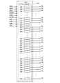
- FIG. 3 is a block diagram showing a configuration of a shift register in a gate driver in the first embodiment.
- FIG. 3 is a block diagram showing a configuration of a shift register in a gate driver in the first embodiment.
- FIG. 4 is a diagram illustrating input / output signals of a first unit circuit in the first embodiment.
- FIG. 3 is a circuit diagram showing a configuration of a first unit circuit in the first embodiment.
- FIG. 3 is a circuit diagram showing a configuration of a second unit circuit in the first embodiment.
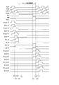
- 6 is a timing chart for explaining basic operations of the first unit circuit in the first embodiment. 6 is a timing chart for explaining a basic operation of a second unit circuit in the first embodiment. 4 is a timing chart for explaining an operation when a halfway stop of scanning is performed in the first embodiment.
- 5 is a timing chart showing a waveform of an output signal when scanning is stopped halfway in the first embodiment. 5 is a timing chart for explaining the driving of the shift register when it is desired to provide two touch processing periods in one frame period (one vertical scanning period) in the first embodiment.
- the 2nd Embodiment of this invention it is a block diagram which shows the structure of the shift register in a gate driver.
- FIG. 6 is a block diagram showing a configuration of a shift register in a gate driver in the second embodiment. It is a circuit diagram which shows the structure of the 1st unit circuit in the said 2nd Embodiment. It is a circuit diagram which shows the structure of the 2nd unit circuit in the said 2nd Embodiment. 10 is a timing chart for explaining an operation when a scan is stopped halfway in the second embodiment. It is FIG. 9 of Japanese Unexamined Patent Publication No. 2014-182203. It is FIG. 10 of Japanese Unexamined Patent Publication No. 2014-182203.
- the gate terminal (gate electrode) of the thin film transistor corresponds to the control terminal
- the drain terminal (drain electrode) corresponds to the first conduction terminal
- the source terminal (source electrode) corresponds to the second conduction terminal.
- a high level corresponds to an on level
- a low level corresponds to an off level.
- the higher of the drain and the source is called the drain, but in the description of this specification, one is defined as the drain and the other is defined as the source. May be higher.
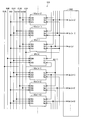
- FIG. 2 is a block diagram showing the overall configuration of the active matrix liquid crystal display device according to the first embodiment of the present invention.
- the liquid crystal display device includes a display control circuit 100, a source driver (video signal line driving circuit) 200, a gate driver (scanning signal line driving circuit) 300, a common electrode driving circuit 400, and a display unit 500.
- the gate driver 300 and the display unit 500 are formed on the same substrate (TFT substrate which is one of the two substrates constituting the liquid crystal panel). That is, the gate driver 300 in this embodiment is a monolithic gate driver.
- TFT substrate which is one of the two substrates constituting the liquid crystal panel.
- the gate driver 300 in this embodiment is a monolithic gate driver.
- the display unit 500 includes a plurality (j) of source bus lines (video signal lines) SL1 to SLj and a plurality (i) of gate bus lines (scanning signal lines) GL1 to GLi. .
- a pixel forming portion 5 for forming pixels is provided corresponding to each intersection of the source bus lines SL1 to SLj and the gate bus lines GL1 to GLj.
- the display unit 500 includes a plurality (i ⁇ j) of pixel forming units 5.
- the plurality of pixel forming portions 5 are arranged in a matrix and constitute an i row ⁇ j column pixel matrix (pixel array).
- the symbol GL is used when it is not necessary to specify a row.
- Each pixel forming portion 5 has a thin film transistor (TFT) which is a switching element having a gate terminal connected to a gate bus line GL passing through a corresponding intersection and a source terminal connected to a source bus line SL passing through the intersection.
- TFT thin film transistor
- the pixel electrode 51 connected to the drain terminal of the thin film transistor 50
- the common electrode 54 and the auxiliary capacitance electrode 55 provided in common to the plurality of pixel forming portions 5, and the pixel electrode 51 and the common electrode 54
- the liquid crystal capacitor 52 and the auxiliary capacitor 53 constitute a pixel capacitor 56. Note that only the components corresponding to one pixel forming portion 5 are shown in the display portion 500 in FIG.
- a configuration in which at least a part of the gate driver 300 is provided in the pixel array (in the display unit 500) may be employed.
- the occurrence of waveform rounding of the scanning signal applied to the gate bus lines GL1 to GLj is suppressed, and the gate bus lines GL1 to GLj can be driven at high speed.
- all the thin film transistors 50 in the pixel forming portion 5 are n-channel type.
- the thin film transistor 50 employs an oxide TFT (a thin film transistor using an oxide semiconductor for a channel layer). Further, in this embodiment, a channel etch type is adopted for the structure of the thin film transistor 50. However, an etch stop type can also be adopted. The same applies to the thin film transistors in the gate driver 300.
- the channel etch type and the etch stop type will be described.
- the etch stop layer is not formed on the channel region, and the lower surface of the end of the source electrode and the drain electrode on the channel side is an oxide semiconductor layer. It arrange
- a channel etch type TFT is formed, for example, by forming a conductive film for a source / drain electrode on an oxide semiconductor layer and performing source / drain separation. In the source / drain separation step, the surface portion of the channel region may be etched.
- the lower surfaces of the end portions on the channel side of the source electrode and the drain electrode are located on the etch stop layer, for example.
- a conductive film for a source / drain electrode is formed on the oxide semiconductor layer and the etch stop layer.
- the oxide semiconductor included in the oxide semiconductor layer may be an amorphous oxide semiconductor or a crystalline oxide semiconductor having a crystalline portion.
- Examples of the crystalline oxide semiconductor include a polycrystalline oxide semiconductor, a microcrystalline oxide semiconductor, and a crystalline oxide semiconductor in which the c-axis is oriented substantially perpendicular to the layer surface.
- the oxide semiconductor layer may have a stacked structure of two or more layers.
- the oxide semiconductor layer may include an amorphous oxide semiconductor layer and a crystalline oxide semiconductor layer.
- the oxide semiconductor layer may include a plurality of crystalline oxide semiconductor layers having different crystal structures.
- the oxide semiconductor layer may include a plurality of amorphous oxide semiconductor layers.
- the energy gap of the oxide semiconductor included in the upper layer is preferably larger than the energy gap of the oxide semiconductor included in the lower layer.
- the energy gap of the lower oxide semiconductor may be larger than the energy gap of the upper oxide semiconductor.
- Japanese Unexamined Patent Application Publication No. 2014-007399 discloses a material, a structure, a film formation method, a structure of an oxide semiconductor layer having a stacked structure, and the like of the amorphous oxide semiconductor and each crystalline oxide semiconductor described above. Are listed.
- the oxide semiconductor layer may contain at least one metal element of In (indium), Ga (gallium), and Zn (zinc), for example.
- the oxide semiconductor layer includes, for example, an In—Ga—Zn—O-based semiconductor (eg, indium gallium zinc oxide).
- the In—Ga—Zn—O-based semiconductor is a ternary oxide of In, Ga, and Zn.
- Such an oxide semiconductor layer can be formed using an oxide semiconductor film containing an In—Ga—Zn—O-based semiconductor.
- a channel-etch TFT having an active layer containing an oxide semiconductor (OS) such as an In—Ga—Zn—O-based semiconductor may be referred to as a “CE-OS-TFT”.
- the In—Ga—Zn—O-based semiconductor may be amorphous or crystalline.
- a crystalline In—Ga—Zn—O-based semiconductor with a c-axis oriented substantially perpendicular to the layer surface is preferably used.
- the crystal structure of a crystalline In—Ga—Zn—O-based semiconductor is, for example, Japanese Unexamined Patent Publication No. 2014-007399, Japanese Unexamined Patent Publication No. 2012-134475, Japanese Unexamined Patent Publication No. 2014-209727. And the like.
- a TFT having an In—Ga—Zn—O-based semiconductor layer has high mobility (mobility more than 20 times that of an a-Si TFT) and low leakage current (leakage less than 1/100 of that of an a-Si TFT). Therefore, it is suitably used as a driving TFT (for example, a thin film transistor in the gate driver 300) and a pixel TFT (the thin film transistor 50).
- the oxide semiconductor layer may include another oxide semiconductor instead of the In—Ga—Zn—O-based semiconductor.
- the oxide semiconductor layer may include, for example, an In—Sn—Zn—O-based semiconductor (eg, In 2 O 3 —SnO 2 —ZnO; InSnZnO).
- the In—Sn—Zn—O-based semiconductor is a ternary oxide of In (indium), Sn (tin), and Zn (zinc).
- the oxide semiconductor layer includes an In—Al—Zn—O based semiconductor, an In—Al—Sn—Zn—O based semiconductor, a Zn—O based semiconductor, an In—Zn—O based semiconductor, and a Zn—Ti—O based semiconductor.
- Cd—Ge—O based semiconductor Cd—Pb—O based semiconductor, CdO (cadmium oxide), Mg—Zn—O based semiconductor, In—Ga—Sn—O based semiconductor, In—Ga—O based semiconductor, A Zr—In—Zn—O based semiconductor, an Hf—In—Zn—O based semiconductor, or the like may be included.
- the display control circuit 100 receives an image signal DAT and a timing signal group TG such as a horizontal synchronization signal and a vertical synchronization signal sent from the outside, and operates the digital video signal DV and the operation of the source driver 200.
- a source control signal SCTL for controlling and a gate control signal GCTL for controlling the operation of the gate driver 300 are output.
- the source control signal SCTL includes a source start pulse signal, a source clock signal, and a latch strobe signal.
- the gate control signal GCTL will be described later.
- the source driver 200 receives the digital video signal DV and the source control signal SCTL output from the display control circuit 100, and applies driving video signals to the source bus lines SL1 to SLj. At this time, the source driver 200 sequentially holds the digital video signal DV indicating the voltage to be applied to each source bus line SL at the timing when the pulse of the source clock signal is generated. The held digital video signal DV is converted into an analog voltage at the timing when the pulse of the latch strobe signal is generated. The converted analog voltage is simultaneously applied to all the source bus lines SL as a driving video signal.
- the gate driver 300 Based on the gate control signal GCTL output from the display control circuit 100, the gate driver 300 sequentially applies active scanning signals one by one to the gate bus lines GL1 to GLi (selects one by one sequentially). ). That is, the gate driver 300 scans the gate bus line GL. At that time, scanning is stopped halfway at a predetermined timing. A detailed description of the gate driver 300 will be described later.
- the common electrode drive circuit 400 gives a predetermined potential Vcom to the common electrode 54c.
- the driving video signals are applied to the source bus lines SL1 to SLj, the scanning signals are applied to the gate bus lines GL1 to GLi, and the predetermined potential Vcom is applied to the common electrode 54.
- An image based on the image signal DAT sent from the outside is displayed on the display unit 500.
- the gate driver 300 includes a shift register 310 having a plurality of stages.
- the shift register 310 includes a first unit circuit UCa that is a unit circuit connected to the gate bus line GL and a second unit that is a unit circuit not connected to the gate bus line GL. Circuit UCb.
- the scan of the gate bus line GL is sequentially performed row by row from the first row to the i-th row.
- the second unit circuit UCb is provided in order to make it possible to stop such scanning halfway.
- the first unit circuit UCa corresponding to the 50th row gate bus line GL50 is used.
- a second unit circuit UCb is provided between the first unit circuit UCa and the first unit circuit UCa.
- the gate driver 300 includes two gate start pulse signals GSP1, GSP2, four gate clock signals CLK1, CLK1B, CLK2, and CLK2B, and three signals CLR, CLRL and RSM and a low-level power supply voltage VSS are applied. Note that the magnitude of the potential applied based on the low-level power supply voltage VSS is referred to as “VSS potential” for convenience.
- FIG. 4 and 5 are block diagrams showing the configuration of the shift register 310 in the gate driver 300 in the present embodiment. Here, it is assumed that scanning is stopped halfway after selection of the nth gate bus line GLn.
- FIG. 4 is a diagram for explaining the configuration of the first unit circuit UCa arranged outside the vicinity of the second unit circuit UCb
- FIG. 5 shows the second unit circuit UCb and the second unit circuit UCb. It is a figure for demonstrating the structure of 1st unit circuit UCa arrange
- FIG. 4 shows first unit circuits UCa (1) to UCa (4) corresponding to the gate bus lines GL1 to GL4 from the first row to the fourth row.
- FIG. 5 shows the first unit circuit UCa (n-2) corresponding to the gate bus lines GLn-2 to GLn from the second unit circuit UCb (n), (n-2) th row to the nth row.
- the first unit circuit UCa has an input terminal for receiving a first clock signal CKA and a second clock signal CKB, which are two-phase clock signals, and a low-level power source.
- An input terminal for receiving the voltage VSS, an input terminal for receiving the set signal Sa, an input terminal for receiving the reset signal Ra, and an output terminal for outputting the output signal (shift pulse) Qa are provided. ing.
- the signals given to the input terminals of the first unit circuits UCa will be described. Note that the low-level power supply voltage VSS is commonly applied to all the first unit circuits UCa (1) to UCa (i).
- the first clock signal CKA and the second clock signal CKB are given to the first unit circuit UCa as follows.
- the gate clock signal CLK1 is supplied as the first clock signal CKA
- the gate clock signal CLK1B is supplied as the second clock signal CKB.
- the gate clock signal CLK2 is supplied as the first clock signal CKA
- the gate clock signal CLK2B is supplied as the second clock signal CKB.
- the gate clock signal CLK1B is supplied as the first clock signal CKA
- the gate clock signal CLK1 is supplied as the second clock signal CKB.
- the gate clock signal CLK2B is supplied as the first clock signal CKA
- the gate clock signal CLK2 is supplied as the second clock signal CKB.
- the set signal Sa is given to the first unit circuit UCa as follows (see FIG. 6). Focusing on the first unit circuit UCa (k) corresponding to the gate bus line GLk in the k-th row (k is an integer between 1 and i), the first unit circuit UCa (k ⁇ 2) in the previous two stages The output signal Qa (k-2) from) is given as the set signal Sa. However, the gate start pulse signal GSP1 is given as the set signal Sa for the first unit circuit UCa (1), and the gate start pulse signal GSP2 is given as the set signal Sa for the first unit circuit UCa (2).
- the output signal Qb (n) from the second unit circuit UCb (n) is given as the set signal Sa.
- the first unit circuit UCa (2) may have a configuration in which the gate start pulse signal GSP1 is given as the set signal Sa instead of the gate start pulse signal GSP2.
- the reset signal Ra is given to the first unit circuit UCa as follows (see FIG. 6). Focusing on the first unit circuit UCa (k) corresponding to the k-th gate bus line GLk, the output signal Qa (k + 3) from the first unit circuit UCa (k + 3) after the third stage is used as the reset signal Ra. Given. However, the first unit circuit UCa (n-2), the first unit circuit UCa (n-1), the first unit circuit UCa (n), the first unit circuit UCa (i-2), the first For the unit circuit UCa (i ⁇ 1) and the first unit circuit UCa (i), the signal CLR is supplied as the reset signal Ra.
- the signal CLRL is given as the reset signal Rb
- the gate clock signal CLK1 is given as the control signal Z
- the output signal Qa (n) from the first unit circuit UCa (n) is given as the set signal Sb
- the signal RSM And a low-level power supply voltage VSS is applied.
- an output signal from the second unit circuit UCb may be given to the touch panel, and the output signal may be used for processing on the touch panel. As a result, the output signal from the second unit circuit UCb can be efficiently used.
- FIG. 7 is a circuit diagram showing a configuration of the first unit circuit UCa in the present embodiment.
- the first unit circuit UCa includes seven thin film transistors T1a to T7a and one capacitor C1a.
- the first unit circuit UCa has four input terminals 61 to 64 and one output terminal 69 in addition to the input terminal for the low-level power supply voltage VSS.
- An input terminal that receives the set signal Sa is denoted by reference numeral 61
- an input terminal that receives the reset signal Ra is denoted by reference numeral 62
- an input terminal that receives the first clock signal CKA is denoted by reference numeral 63
- the input terminal that receives the 2-clock signal CKB is denoted by reference numeral 64.
- An output terminal for outputting the output signal Qa is denoted by reference numeral 69.
- the source terminal of the thin film transistor T1a, the drain terminal of the thin film transistor T2a, the gate terminal of the thin film transistor T3a, the drain terminal of the thin film transistor T4a, and the gate terminal of the thin film transistor T6a are connected to each other.
- the internal node where these are connected to each other is denoted by reference numeral N1a.
- the gate terminal of the thin film transistor T4a, the source terminal of the thin film transistor T5a, and the drain terminal of the thin film transistor T6a are connected to each other.
- An internal node where these are connected to each other is denoted by reference numeral N2a.
- the gate terminal and the drain terminal are connected to the input terminal 61 (that is, diode connection), and the source terminal is connected to the internal node N1a.
- the gate terminal is connected to the input terminal 62
- the drain terminal is connected to the internal node N1a
- the source terminal is connected to the input terminal for the power supply voltage VSS.
- the gate terminal is connected to the internal node N1a
- the drain terminal is connected to the input terminal 63
- the source terminal is connected to the output terminal 69.
- the gate terminal is connected to the node N2a, the drain terminal is connected to the internal node N1a, and the source terminal is connected to the input terminal for the power supply voltage VSS.
- the gate terminal and the drain terminal are connected to the input terminal 64 (that is, diode connection), and the source terminal is connected to the node N2a.
- the gate terminal is connected to the internal node N1a, the drain terminal is connected to the node N2a, and the source terminal is connected to the input terminal for the power supply voltage VSS.
- the gate terminal is connected to the input terminal 64, the drain terminal is connected to the output terminal 69, and the source terminal is connected to the input terminal for the power supply voltage VSS.
- the capacitor C1a has one end connected to the internal node N1a and the other end connected to the output terminal 69.
- the thin film transistor T1a changes the potential of the internal node N1a toward the high level when the set signal Sa is at the high level.
- the thin film transistor T2a changes the potential of the internal node N1a toward the VSS potential when the reset signal Ra is at a high level.
- the thin film transistor T3a applies the potential of the first clock signal CKA to the output terminal 69 when the potential of the internal node N1a is at a high level.
- the thin film transistor T4a changes the potential of the internal node N1a toward the VSS potential when the potential of the internal node N2a is at a high level.
- the thin film transistor T5a changes the potential of the internal node N2a toward the high level when the second clock signal CKB is at the high level.
- the thin film transistor T6a changes the potential of the internal node N2a toward the VSS potential when the potential of the internal node N1a is at a high level.
- the thin film transistor T7a changes the potential of the output signal Qa (the potential of the output terminal 69) toward the VSS potential when the second clock signal CKB is at a high level.
- Capacitor C1a functions as a bootstrap capacitor for increasing the potential of internal node N1a as the potential of output terminal 69 increases.
- first output control node stabilizing unit 312a for maintaining the level is realized.
- the configuration of the first output control node stabilizing unit 312a shown in FIG. 7 is an example, and the present invention is not limited to this.
- the thin film transistor T7a realizes a circuit 314a (hereinafter referred to as “first output node stabilizing section”) 314a for maintaining the potential of the output signal Qa (the potential of the output terminal 69) at a low level throughout the non-selection period. Yes.
- first output node stabilizing section a circuit 314a (hereinafter referred to as “first output node stabilizing section”) 314a for maintaining the potential of the output signal Qa (the potential of the output terminal 69) at a low level throughout the non-selection period.
- the first output control node turn-on transistor is realized by the thin film transistor T1a
- the first output control node turn-off transistor is realized by the thin film transistor T2a
- the first output control transistor is realized by the thin film transistor T3a.
- the first capacitance is realized by the capacitor C1a.
- the output terminal 69 implements a first output node
- the internal node N1a implements a first output control node.
- FIG. 8 is a circuit diagram showing a configuration of the second unit circuit UCb in the present embodiment.
- the second unit circuit UCb includes seven thin film transistors T1b to T7b and one capacitor C1b.
- the second unit circuit UCb has four input terminals 71 to 74 and one output terminal 79 in addition to the input terminal for the low-level power supply voltage VSS.
- the input terminal that receives the set signal Sb is denoted by reference numeral 71
- the input terminal that receives the reset signal Rb is denoted by reference numeral 72
- the input terminal that receives the signal RSM is denoted by reference numeral 73
- the control signal Z is assigned.
- the receiving input terminal is denoted by reference numeral 74.
- reference numeral 79 is attached to an output terminal for outputting the output signal Qb.
- the source terminal of the thin film transistor T1b, the drain terminal of the thin film transistor T2b, the gate terminal of the thin film transistor T3b, the drain terminal of the thin film transistor T4b, and the gate terminal of the thin film transistor T6b are connected to each other.
- An internal node where these are connected to each other is denoted by reference numeral N1b.
- the gate terminal of the thin film transistor T4b, the source terminal of the thin film transistor T5b, and the drain terminal of the thin film transistor T6b are connected to each other.
- An internal node where these are connected to each other is denoted by reference numeral N2b.
- the gate terminal and the drain terminal are connected to the input terminal 71 (that is, diode connection), and the source terminal is connected to the internal node N1b.
- the gate terminal is connected to the input terminal 72
- the drain terminal is connected to the internal node N1b
- the source terminal is connected to the input terminal for the power supply voltage VSS.
- the gate terminal is connected to the internal node N1b
- the drain terminal is connected to the input terminal 73
- the source terminal is connected to the output terminal 79.
- the gate terminal is connected to the node N2b, the drain terminal is connected to the internal node N1b, and the source terminal is connected to the input terminal for the power supply voltage VSS.
- the gate terminal and the drain terminal are connected to the input terminal 74 (that is, diode connection), and the source terminal is connected to the node N2b.
- the gate terminal is connected to the internal node N1b, the drain terminal is connected to the node N2b, and the source terminal is connected to the input terminal for the power supply voltage VSS.
- the gate terminal is connected to the input terminal 74, the drain terminal is connected to the output terminal 79, and the source terminal is connected to the input terminal for the power supply voltage VSS.
- One end of the capacitor C1b is connected to the internal node N1b, and the other end is connected to the output terminal 79.
- the thin film transistor T1b changes the potential of the internal node N1b toward the high level when the set signal Sb is at the high level.
- the thin film transistor T2b changes the potential of the internal node N1b toward the VSS potential when the reset signal Ra is at a high level.
- the thin film transistor T3b applies the potential of the signal RSM to the output terminal 79 when the potential of the internal node N1b is at a high level.
- the thin film transistor T4b changes the potential of the internal node N1b toward the VSS potential when the potential of the internal node N2b is at a high level.
- the thin film transistor T5b changes the potential of the internal node N2b toward the high level when the control signal Z is at the high level.
- the thin film transistor T6b changes the potential of the internal node N2b toward the VSS potential when the potential of the internal node N1b is at a high level.
- the thin film transistor T7b changes the potential of the output signal Qb (the potential of the output terminal 79) toward the VSS potential when the control signal Z is at a high level.
- Capacitor C1b functions as a bootstrap capacitor for increasing the potential of internal node N1b as the potential of output terminal 79 increases.
- the thin film transistor T4b, the thin film transistor T5b, and the thin film transistor T6b is a circuit for maintaining the potential of the node N1b at a low level throughout a period other than a touch processing period described later (except for a period just before the touch processing period).
- a “second output control node stabilizing unit” 312b is realized.
- the configuration of the second output control node stabilizing unit 312b illustrated in FIG. 8 is an example, and the present invention is not limited to this.
- second output node stabilizing unit 314b a circuit for maintaining the potential of the output signal Qb (the potential of the output terminal 79) at a low level throughout the period other than the period before the end of the touch processing period by the thin film transistor T7b (hereinafter referred to as “second output node stabilizing unit”). 314b) is realized.
- the configuration of the second output node stabilizing unit 314b illustrated in FIG. 8 is an example, and the present invention is not limited to this.
- the second output control node turn-on transistor is realized by the thin film transistor T1b
- the second output control node turn-off transistor is realized by the thin film transistor T2b
- the second output control transistor is realized by the thin film transistor T3b.
- a second capacitance is realized by the capacitor C1b.
- the output terminal 79 implements a second output node
- the internal node N1b implements a second output control node.
- FIG. 9 is a timing chart for explaining the basic operation of the first unit circuit UCa.
- FIG. 10 is a timing chart for explaining the basic operation of the second unit circuit UCb.
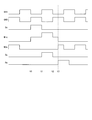
- FIG. 11 is a timing chart for explaining the operation when the scanning is stopped halfway.
- FIG. 12 is a timing chart showing waveforms of the output signals Qa and Qb when scanning is stopped halfway.
- FIG. 13 is a timing chart for explaining the driving of the shift register when it is desired to provide two touch processing periods in one frame period (one vertical scanning period).
- the first clock signal CKA changes from the low level to the high level.
- the thin film transistor T3a since the thin film transistor T3a is in an on state, the potential of the output terminal 69 increases as the potential of the input terminal 63 increases.
- the capacitor C1a is provided between the internal node N1a and the output terminal 69, the potential of the internal node N1a increases as the potential of the output terminal 69 increases (the internal node N1a is boosted). State).
- a large voltage is applied to the thin film transistor T3a, and the potential of the output signal Qa rises to the high level potential of the first clock signal CKA.
- the gate bus line GL connected to the output terminal 69 of the first unit circuit UCa is selected.
- the set signal Sa changes from the high level to the low level at time t1.
- the thin film transistor T1a is turned off. The turning off of the thin film transistor T1a does not affect the potential of the internal node N1a.
- the first clock signal CKA changes from the high level to the low level.
- the potential of the output terminal 69 decreases as the potential of the input terminal 63 decreases, and the potential of the internal node N1a also decreases via the capacitor C1a.
- the second clock signal CKB changes from the low level to the high level. Thereby, the thin film transistor T7a is turned on. From the above, the potential of the output terminal 69, that is, the potential of the output signal Qa becomes low level.
- the internal node N1a since the potential of the internal node N1a is at a high level, even if the thin film transistor T5a is turned on by the second clock signal CKB being at a high level, the internal node The potential of N2a is maintained at a low level. Therefore, the potential of the internal node N1a does not fall to the low level during the period from the time point t0 to the time point t3.
- the second clock signal CKB is at the low level, so that the thin film transistor T7a is maintained in the off state. For this reason, the potential of the output signal Qa does not fall to a low level during this period.
- the potential of the internal node N2a becomes high level when the second clock signal CKB is high level. That is, the thin film transistor T4a is turned on every predetermined period.
- the potential of the internal node N1a is pulled to the VSS potential every predetermined period.
- the potential of the output terminal 69 is pulled to the VSS potential every predetermined period.
- Second Unit Circuit ⁇ 1.4.2 Operation of Second Unit Circuit>
- the gate bus line GL is scanned during the period before time t10.
- the potential of the internal node N1b and the potential of the output signal Qb are low level, and the potential of the internal node N2b is high level.
- a pulse (shift pulse) of the set signal Sb is given to the input terminal 71. Since the thin film transistor T1b is diode-connected as shown in FIG. 8, the thin film transistor T1b is turned on by the pulse of the set signal Sb, and the capacitor C1b is charged. As a result, the potential of the internal node N1b changes from the low level to the high level, and the thin film transistor T3b is turned on. Incidentally, the signal RSM is maintained at the low level during the period from the time point t10 to the time point t11. Therefore, during this period, the output signal Qb is maintained at a low level.
- the set signal Sb changes from the high level to the low level.
- the thin film transistor T1b is turned off.
- the signal RSM is maintained at the low level. Therefore, during this period, the output signal Qb is maintained at a low level.
- the signal RSM changes from low level to high level.
- the thin film transistor T3b since the thin film transistor T3b is in the on state, the potential of the output terminal 79 increases as the potential of the input terminal 73 increases.
- the capacitor C1b since the capacitor C1b is provided between the internal node N1b and the output terminal 79, the potential of the internal node N1b increases as the potential of the output terminal 79 increases (the internal node N1b is boosted). State).
- a large voltage is applied to the thin film transistor T3b, and the potential of the output signal Qb rises to the high level potential of the signal RSM.
- the signal RSM changes from high level to low level.
- the potential of the output terminal 79 decreases as the potential of the input terminal 73 decreases, and the potential of the internal node N1b also decreases via the capacitor C1b.
- the reset signal Rb changes from the low level to the high level.
- the thin film transistor T2b is turned on.
- the potential of the internal node N1b becomes low level.
- the control signal Z changes from the low level to the high level.
- the thin film transistor T7b is turned on.
- the potential of the output signal Qb becomes low level.
- the output signal Qa (n-3) and the output signal Qa (n-2) are at the high level, and the internal nodes N1a (n-3) and N1a (n-2) ), The potentials of the internal node N1a (n ⁇ 1) and the internal node N1a (n) are at a high level.
- the gate clock signal CLK1 changes from high level to low level, and the gate clock signal CLK1B changes from low level to high level.
- the output signal Qa (n-3) becomes low level and the output signal Qa (n-1) becomes high level.
- the gate clock signal CLK2 changes from high level to low level
- the gate clock signal CLK2B changes from low level to high level.
- the output signal Qa (n-2) becomes low level
- the output signal Qa (n) becomes high level.
- the output signal Qa (n) is given to the first unit circuit UCa (n-3) as the reset signal Ra
- the potential of the internal node N1a (n-3) becomes low level.
- the output signal Qa (n) is given to the second unit circuit UCb (n) as the set signal Sb, the potential of the internal node N1b (n) becomes high level.
- the gate clock signal CLK1B changes from the high level to the low level. As a result, the output signal Qa (n ⁇ 1) becomes low level. At time t22, the gate clock signal CLK1 is maintained at a low level.
- the gate clock signal CLK2B changes from the high level to the low level.
- the output signal Qa (n) becomes low level.
- the signal CLR changes from the low level to the high level.
- the signal CLR is supplied as a reset signal Ra to the first unit circuit UCa (n-2), the first unit circuit UCa (n-1), and the first unit circuit UCa (n).
- the potentials of the internal node N1a (n-2), the internal node N1a (n-1), and the internal node N1a (n) become low level. In this way, at time t23, scanning of the gate bus line GL is stopped.
- the signal CLR changes from high level to low level.
- the change in the level of the signal CLR at time t24 does not affect the operation of the first unit circuit UCa.
- the signal RSM changes from low level to high level.
- the internal node N1b (n) is in the boost state, and the output signal Qb (n) is at the high level. Since the output signal Qb (n) is supplied as the set signal Sa to the first unit circuit UCa (n + 1) and the first unit circuit UCa (n + 2), the potentials of the internal node N1a (n + 1) and the internal node N1a (n + 2) becomes high level.
- the signal RSM changes from high level to low level
- the signal CLRL changes from low level to high level.
- the output signal Qb (n) becomes low level
- the potential of the internal node N1b (n) becomes low level.
- the gate clock signal CLK1 changes from the low level to the high level.
- the internal node N1a (n + 1) is in the boost state, and the output signal Qa (n + 1) is at the high level.
- the signal CLRL becomes low level at time t28.
- the gate clock signal CLK2 changes from the low level to the high level.
- the internal node N1a (n + 2) is in a boost state, and the output signal Qa (n + 2) is at a high level. In this way, scanning of the gate bus line GL is resumed.
- the signal CLR is set to the high level at the time when the touch processing period should be started,
- the clock operation of the gate clock signal may be stopped throughout the period to be the touch processing period.
- the signal RSM is set to a high level slightly before the time point at which the touch processing period should end
- the signal CLRL is set to a high level at the time point at which the touch processing period should end
- the gate clock signal The clock operation may be resumed.
- the shift operation stop step is realized by the operation at time t23
- the shift operation restart step is realized by the operations at time t25 and time t26.
- the first unit circuit UCa and the second unit circuit UCb have different input signals but the same circuit configuration.
- the first unit circuit UCa and the second unit circuit UCb only the first unit circuit UCa is connected to the gate bus line GL (see FIG. 1). Therefore, the first unit circuit UCa needs to drive a larger load than the second unit circuit UCb.
- the sizes of the thin film transistor T1a, the thin film transistor T2a, the thin film transistor T3a, the thin film transistor T1b, the thin film transistor T2b, and the thin film transistor T3b are respectively S (T1a), S (T2a), S (T3a), S (T1b), S (T2b), and This is represented by S (T3b).
- the shift register 310 is a second unit circuit having a configuration similar to that of the conventional unit circuit (first unit circuit UCa) as a unit circuit for enabling a halfway stop of scanning.
- Unit circuit UCb is provided.
- the signal RSM and the signal CLRL are necessary for the operation of the second unit circuit UCb. In this way, it is possible to stop scanning halfway only by providing two new signals as compared with the conventional case.
- threshold shift between a transistor in a unit circuit arranged at a position where scanning is stopped and a transistor in another unit circuit is performed. Display failure occurs due to the difference in the size of.
- the second unit circuit UCb since the internal node N1b of the second unit circuit UCb is maintained at a high level while scanning is stopped, a large threshold shift occurs in the thin film transistor Tb3.
- the second unit circuit UCb It is not connected to the bus line GL. For this reason, the large threshold shift generated in the thin film transistor Tb3 does not affect the display quality.
- a shift register capable of stopping scanning halfway without causing a display defect is realized.
- the first unit circuit UCa is provided with the first output control node stabilizing unit 312a for maintaining the potential of the node N1a at a low level throughout the non-selection period.
- the unit circuit UCb is provided with a second output control node stabilizing unit 312b for maintaining the potential of the node N1b at a low level throughout a period other than the touch processing period (except for a period just before the touch processing period). It has been. For this reason, even if noise is mixed in the node N1a and the node N1b, the occurrence of abnormal operation due to the noise is suppressed.
- the first unit circuit UCa has the first output node stabilizing unit 314a for maintaining the potential of the output signal Qa (the potential of the output terminal 69) at a low level throughout the non-selection period.
- the second unit circuit UCb includes a second output node for maintaining the potential of the output signal Qb (the potential of the output terminal 79) at a low level throughout a period other than the period before the end of the touch processing period.
- a stabilizing portion 314b is provided. For this reason, even if noise is mixed in the output terminal 69 or the output terminal 79, the occurrence of abnormal operation due to the noise is suppressed.
- Second Embodiment> A second embodiment of the present invention will be described. The overall configuration and operation outline are the same as those in the first embodiment, and a description thereof will be omitted (see FIG. 2). Also in this embodiment, it is assumed that the liquid crystal panel constituting the display unit 500 is integrated with the touch panel.
- the gate driver 300 is configured by a shift register 310 having a plurality of stages, and the shift register 310 is a first circuit that is a unit circuit connected to the gate bus line GL.
- Unit circuit UCa and a second unit circuit UCb which is a unit circuit not connected to the gate bus line GL (see FIG. 1).
- FIG. 14 and 15 are block diagrams showing the configuration of the shift register 310 in the gate driver 300 in the present embodiment.
- FIG. 14 is a diagram for explaining the configuration of the first unit circuit UCa arranged outside the vicinity of the second unit circuit UCb.
- FIG. 15 shows the second unit circuit UCb and the second unit circuit UCb. It is a figure for demonstrating the structure of 1st unit circuit UCa arrange
- the first unit circuit UCa is provided with an input terminal for receiving the signal CLR in addition to the input terminal provided in the first embodiment.
- the second unit circuit UCb is provided with an input terminal for receiving the signal CLRL in addition to the input terminal provided in the first embodiment.
- FIG. 16 is a circuit diagram showing a configuration of the first unit circuit UCa in the present embodiment.
- the first unit circuit UCa is provided with a thin film transistor T8a, a thin film transistor T9a, a thin film transistor T10a, and an input terminal 65 in addition to the components in the first embodiment.
- a signal CLR is given to the input terminal 65.
- the gate terminal is connected to the input terminal 65, the drain terminal is connected to the internal node N1a, and the source terminal is connected to the input terminal for the power supply voltage VSS.
- the gate terminal is connected to the input terminal 65, the drain terminal is connected to the output terminal 69, and the source terminal is connected to the input terminal for the power supply voltage VSS.
- the gate terminal is connected to the input terminal 65, the drain terminal is connected to the internal node N2a, and the source terminal is connected to the input terminal for the power supply voltage VSS.
- the thin film transistor T8a changes the potential of the internal node N1a toward the VSS potential when the signal CLR is at a high level.
- the thin film transistor T9a changes the potential of the output signal Qa (the potential of the output terminal 69) toward the VSS potential when the signal CLR is at a high level.
- the thin film transistor T10a changes the potential of the internal node N2a toward the VSS potential when the signal CLR is at a high level.
- the first output control node stabilizing unit 312a is realized by the thin film transistor T4a, the thin film transistor T5a, the thin film transistor T6a, and the thin film transistor T10a. Further, the first output control node off maintaining transistor is realized by the thin film transistor T8a, and the first output node off maintaining transistor is realized by the thin film transistor T9a.
- FIG. 17 is a circuit diagram showing a configuration of the second unit circuit UCb in the present embodiment.
- the second unit circuit UCb is provided with a thin film transistor T8b, a thin film transistor T9b, a thin film transistor T10b, and an input terminal 75 in addition to the components in the first embodiment.
- the input terminal 75 is supplied with a signal CLRL.
- the gate terminal is connected to the input terminal 75, the drain terminal is connected to the internal node N1b, and the source terminal is connected to the input terminal for the power supply voltage VSS.
- the gate terminal is connected to the input terminal 75, the drain terminal is connected to the output terminal 79, and the source terminal is connected to the input terminal for the power supply voltage VSS.
- the gate terminal is connected to the input terminal 75, the drain terminal is connected to the internal node N2b, and the source terminal is connected to the input terminal for the power supply voltage VSS.
- the thin film transistor T8b changes the potential of the internal node N1b toward the VSS potential when the signal CLRL is at a high level.
- the thin film transistor T9b changes the potential of the output signal Qb (the potential of the output terminal 79) toward the VSS potential when the signal CLRL is at a high level.
- the thin film transistor T10b changes the potential of the internal node N2b toward the VSS potential when the signal CLRL is at a high level.
- the second output control node stabilizing unit 312b is realized by the thin film transistor T4b, the thin film transistor T5b, the thin film transistor T6b, and the thin film transistor T10b. Further, the second output control node off maintaining transistor is realized by the thin film transistor T8b, and the second output node off maintaining transistor is realized by the thin film transistor T9b.
- the signal given to the input terminal 72 and the signal given to the input terminal 75 are the same. Accordingly, the thin film transistor T8b and the input terminal 75 may be removed from the configuration shown in FIG. 17, and the gate terminal of the thin film transistor T9b and the gate terminal of the thin film transistor T10b may be connected to the input terminal 72.
- the same operation as in the first embodiment is performed except that the signal CLRL changes from the high level to the low level. Note that the change in the level of the signal CLRL at the time point t21 does not affect the operation of the second unit circuit UCb (n).
- the same operation as in the first embodiment is performed.
- the gate clock signal CLK2B changes from the high level to the low level.
- the potential of the output signal Qa (n) becomes low level.
- the signal CLR changes from the low level to the high level.
- the signal CLR is supplied as a reset signal Ra to the first unit circuit UCa (n-2), the first unit circuit UCa (n-1), and the first unit circuit UCa (n).
- the potentials of the internal node N1a (n-2), the internal node N1a (n-1), and the internal node N1a (n) become low level.
- scanning of the gate bus line GL is stopped.
- the signal CLR is supplied to all the first unit circuits UCa in the shift register 310. For this reason, at the time point t23, the thin film transistors T8a, T9a, and T10a are turned on in all the first unit circuits UCa. Thereby, in all the first unit circuits UCa, the potential of the internal node N1a, the potential of the output terminal 69, and the potential of the internal node N2a are drawn to the VSS potential.
- the signal CLR is maintained at a high level.
- the signal RSM changes from the low level to the high level.
- the output signal Qb (n) is supplied as the set signal Sa to the first unit circuit UCa (n + 1) and the first unit circuit UCa (n + 2), the potentials of the internal node N1a (n + 1) and the internal node N1a (n + 2) Becomes high level.
- the signal CLR changes from the high level to the low level at this time point t25. In this way, in the present embodiment, the signal CLR is maintained at a high level for a longer period than in the first embodiment.
- the signal RSM changes from high level to low level.
- the potential of the output signal Qb (n) becomes low level.
- the gate clock signal CLK1 changes from the low level to the high level.
- the internal node N1a (n + 1) is in the boost state, and the output signal Qa (n + 1) is at the high level.
- the signal CLRL changes from the low level to the high level. Since the signal CLRL is supplied as the reset signal Rb to the second unit circuit UCb (n), the potential of the internal node N1b (n) becomes low level.
- the signal CLRL is given to the gate terminals of the thin film transistor T8b, the thin film transistor T9b, and the thin film transistor T10b.
- the potential of the internal node N1b, the potential of the output terminal 79, and the potential of the internal node N2b are drawn to the VSS potential.
- the same operation as in the first embodiment is performed.
- the signal CLRL is maintained at a high level.
- the signal CLRL is maintained at a high level for a longer period than in the first embodiment.
- the following effects can be obtained.
- the thin film transistors T8a, T9a, and T10a are turned on in all the first unit circuits UCa in the shift register 310. For this reason, it is possible to maintain the potentials of all internal nodes and output nodes in the first unit circuit UCa at the VSS potential while the scan is stopped (when the shift operation is stopped).
- an abnormal operation for example, an abnormal operation caused when the potential of the output signal Qa is increased and the thin film transistor 50 in the pixel forming unit 5 is turned on
- the influence of noise caused by coupling of parasitic capacitance or the like occurs. Is suppressed.
- the thin film transistors T8b, T9b, and T10b are turned on in all the second unit circuits UCb in the shift register 310. Therefore, the potentials of all internal nodes and output nodes in the second unit circuit UCb can be maintained at the VSS potential during the scan period. This makes it possible to prevent an erroneous shift pulse from being output from the second unit circuit UCb to the first unit circuit UCa at the next stage during the period during which scanning is performed. As described above, according to the present embodiment, a shift register that can stop scanning halfway without causing display failure or abnormal operation is realized.
- the liquid crystal display device has been described as an example, but the present invention is not limited to this.
- the present invention can also be applied to other display devices such as an organic EL (Electro Luminescence).
- the specific configuration of the unit circuits (the first unit circuit UCa and the second unit circuit UCb) constituting the shift register 310 is not limited to the configurations shown in the above embodiments.
- the present invention is not limited to this. The present invention can also be applied when a clock signal having a number other than four phases is used as a gate clock signal.
- the touch panel processing is performed while scanning is stopped.
- the present invention is not limited to this.
- the present invention can also be applied when the period during which scanning is stopped is used for processing other than touch panel processing.
Abstract
The purpose of the present invention is to provide a shift register with which a scan can be stopped partway through without creating a defective display or causing abnormal operation. A plurality of unit circuits, which respectively constitute part of a plurality of levels in a shift register (310), are configured from first unit circuits (UCa) that are connected to a gate bus line (GL) and are configured so as to output shift pulses to the connected gate bus line (GL) and to successive levels, and second unit circuits (UCb) that are not connected to the gate bus line (GL) and are configured so as to output shift pulses to successive levels.
Description
本発明は、シフトレジスタに関し、より詳しくは、タッチパネルを備えた表示装置等に設けられるシフトレジスタに関する。
The present invention relates to a shift register, and more particularly to a shift register provided in a display device or the like provided with a touch panel.
従来より、複数本のソースバスライン(映像信号線)および複数本のゲートバスライン(走査信号線)を含む表示部を備えたアクティブマトリクス型の液晶表示装置が知られている。このような液晶表示装置に関し、従来、ゲートバスラインを駆動するためのゲートドライバ(走査信号線駆動回路)は、液晶パネルを構成する基板の周辺部にIC(Integrated Circuit)チップとして搭載されることが多かった。しかしながら、近年、液晶パネルを構成する2枚のガラス基板のうちの一方の基板であるTFT基板上に直接的にゲートドライバを形成することが徐々に多くなされている。このようなゲートドライバは「モノリシックゲートドライバ」などと呼ばれている。
Conventionally, an active matrix type liquid crystal display device having a display unit including a plurality of source bus lines (video signal lines) and a plurality of gate bus lines (scanning signal lines) is known. With respect to such a liquid crystal display device, conventionally, a gate driver (scanning signal line drive circuit) for driving a gate bus line is mounted as an IC (Integrated Circuit) chip on the periphery of a substrate constituting the liquid crystal panel. There were many. However, in recent years, a gate driver is often formed directly on a TFT substrate which is one of two glass substrates constituting a liquid crystal panel. Such a gate driver is called a “monolithic gate driver”.
アクティブマトリクス型の液晶表示装置の表示部には、複数本のソースバスラインと、複数本のゲートバスラインと、それら複数本のソースバスラインと複数本のゲートバスラインとの交差点にそれぞれ対応して設けられた複数個の画素形成部とが形成されている。上記複数個の画素形成部はマトリクス状に配置されて画素アレイを構成している。各画素形成部は、対応する交差点を通過するゲートバスラインにゲート端子が接続されるとともに当該交差点を通過するソースバスラインにソース端子が接続されたスイッチング素子である薄膜トランジスタや、画素電圧値を保持するための画素容量などを含んでいる。アクティブマトリクス型の液晶表示装置には、また、上述したゲートドライバと、ソースバスラインを駆動するためのソースドライバ(映像信号線駆動回路)とが設けられている。
The display portion of the active matrix type liquid crystal display device corresponds to each of a plurality of source bus lines, a plurality of gate bus lines, and intersections of the plurality of source bus lines and the plurality of gate bus lines. And a plurality of pixel formation portions provided. The plurality of pixel forming portions are arranged in a matrix to form a pixel array. Each pixel formation unit holds a thin film transistor, which is a switching element in which a gate terminal is connected to a gate bus line passing through a corresponding intersection and a source terminal is connected to a source bus line passing through the intersection, and a pixel voltage value It includes a pixel capacity and the like. The active matrix liquid crystal display device is also provided with the gate driver described above and a source driver (video signal line driving circuit) for driving the source bus line.
画素電圧値を示す映像信号はソースバスラインによって伝達される。しかしながら、各ソースバスラインは複数行分の画素電圧値を示す映像信号を一時(同時)に伝達することができない。このため、マトリクス状に配置された上述の画素形成部内の画素容量への映像信号の書き込み(充電)は1行ずつ順次に行われる。そこで、複数本のゲートバスラインが所定期間ずつ順次に選択されるように、ゲートドライバは複数段からなるシフトレジスタによって構成されている。そして、シフトレジスタの各段から順次にアクティブな走査信号が出力されることによって、上述のように、画素容量への映像信号の書き込みが1行ずつ順次に行われる。
The video signal indicating the pixel voltage value is transmitted through the source bus line. However, each source bus line cannot transmit video signals indicating pixel voltage values for a plurality of rows at a time (simultaneously). For this reason, the writing (charging) of the video signal to the pixel capacitors in the above-described pixel formation portion arranged in a matrix is sequentially performed row by row. Therefore, the gate driver is constituted by a shift register having a plurality of stages so that a plurality of gate bus lines are sequentially selected for a predetermined period. Then, by sequentially outputting active scanning signals from each stage of the shift register, writing of video signals to the pixel capacitors is sequentially performed row by row as described above.
なお、本明細書においては、シフトレジスタの各段を構成する回路のことを「単位回路」という。また、1行目のゲートバスラインから最終行目のゲートバスラインまでを1本ずつ順次に選択することを単に「スキャン」といい、1行目から最終行目までの途中でスキャンを停止することを「スキャンの途中停止」という。
In this specification, a circuit constituting each stage of the shift register is referred to as a “unit circuit”. Further, selecting one by one sequentially from the first gate bus line to the last gate bus line is simply referred to as “scan”, and the scan is stopped halfway from the first row to the last row. This is called “intermediate scanning stop”.
ところで、近年、タッチパネルと液晶パネルとが一体化した構成の液晶表示装置が普及しつつある。このような液晶表示装置では、スキャンが行われていない時にタッチパネルの処理(例えば、タッチされた位置を検出する処理)を行う必要がある。しかしながら、液晶表示装置に設けられる従来のシフトレジスタは、全ての段が同じように構成されている。このため、1行目のゲートバスラインが選択された後、最終行目のゲートバスラインが選択されるまでは、スキャンを停止することができない。
Incidentally, in recent years, a liquid crystal display device having a configuration in which a touch panel and a liquid crystal panel are integrated is becoming widespread. In such a liquid crystal display device, it is necessary to perform touch panel processing (for example, processing for detecting a touched position) when scanning is not performed. However, the conventional shift register provided in the liquid crystal display device is configured in the same manner in all stages. For this reason, scanning cannot be stopped until the gate bus line of the last row is selected after the gate bus line of the first row is selected.
そこで、日本の特開2014-182203号公報には、スキャンの途中停止を行いたい位置に対応する単位回路(日本の特開2014-182203号公報では「転送回路」と記載)の構成を入力されたシフト信号(シフトパルス)の電位を長期間保持することのできる構成とすることによりスキャンの途中停止を可能にしたシフトレジスタについての発明が開示されている。
Therefore, Japanese Laid-Open Patent Publication No. 2014-182203 inputs the configuration of a unit circuit (described as “transfer circuit” in Japanese Laid-Open Patent Publication No. 2014-182203) corresponding to a position where scanning is to be stopped halfway. Further, there has been disclosed an invention relating to a shift register in which the potential of a shift signal (shift pulse) can be held for a long period of time so that scanning can be stopped halfway.
ところが、日本の特開2014-182203号公報に開示されたシフトレジスタによれば、シフト信号の電位を長期間保持することができない構成の単位回路(第2転送回路)(図19参照)のみならずシフト信号の電位を長期間保持することのできる構成の単位回路(第1転送回路)(図20参照)もゲートバスラインに接続されている。すなわち、第1転送回路からの出力信号も第2転送回路からの出力信号も走査信号としてゲートバスラインに与えられる。このような構成において、第1転送回路ではシフト信号が長期間保持されるので、トランジスタTr1のゲートにバイアスがかかる時間が、第2転送回路よりも第1転送回路の方が長くなる。このため、第1転送回路内のトランジスタTr1の閾値シフトが、第2転送回路内のトランジスタTr1の閾値シフトよりも大きくなる。これにより、第1転送回路に接続されたゲートバスラインと第2転送回路に接続されたゲートバスラインとでは走査信号の波形が異なることとなる。その結果、表示不良が生じる。
However, according to the shift register disclosed in Japanese Patent Application Laid-Open No. 2014-182203, the unit circuit (second transfer circuit) (see FIG. 19) having a configuration that cannot hold the potential of the shift signal for a long period of time can be used. A unit circuit (first transfer circuit) (see FIG. 20) having a configuration capable of holding the potential of the shift signal for a long period is also connected to the gate bus line. That is, both the output signal from the first transfer circuit and the output signal from the second transfer circuit are applied to the gate bus line as scanning signals. In such a configuration, since the shift signal is held in the first transfer circuit for a long period of time, the time required for biasing the gate of the transistor Tr1 is longer in the first transfer circuit than in the second transfer circuit. For this reason, the threshold shift of the transistor Tr1 in the first transfer circuit is larger than the threshold shift of the transistor Tr1 in the second transfer circuit. As a result, the waveform of the scanning signal differs between the gate bus line connected to the first transfer circuit and the gate bus line connected to the second transfer circuit. As a result, display failure occurs.
また、各単位回路(第1転送回路および第2転送回路)は次段の単位回路からの出力信号のみによって内部状態がリセットされる。このため、タッチパネルの処理が行われている期間中に単位回路の内部ノードが電気的に浮いた状態となり、そのような状態が異常動作を引き起こすことが懸念される。
Also, the internal state of each unit circuit (first transfer circuit and second transfer circuit) is reset only by the output signal from the next unit circuit. For this reason, there is a concern that the internal node of the unit circuit is in an electrically floating state during the period when the touch panel processing is performed, and that such a state causes an abnormal operation.
そこで本発明は、表示不良や異常動作を引き起こすことなくスキャンの途中停止を行うことができるシフトレジスタを実現することを目的とする。
Therefore, an object of the present invention is to realize a shift register that can stop scanning halfway without causing display failure or abnormal operation.
本発明の第1の局面は、複数の段からなり、複数のクロック信号に基づきシフト動作を行うことによって複数の走査信号線を駆動するシフトレジスタであって、
前記複数の段のそれぞれを構成する複数の単位回路は、
前記複数の走査信号線の1つに接続され、その接続された走査信号線および後続の段にシフトパルスを出力するように構成された第1の単位回路と、
前記複数の走査信号線のいずれにも接続されず、後続の段にシフトパルスを出力するように構成された第2の単位回路と
を含むことを特徴とする。 A first aspect of the present invention is a shift register that includes a plurality of stages and drives a plurality of scanning signal lines by performing a shift operation based on a plurality of clock signals.
The plurality of unit circuits constituting each of the plurality of stages are:
A first unit circuit connected to one of the plurality of scanning signal lines and configured to output a shift pulse to the connected scanning signal line and a subsequent stage;
And a second unit circuit configured to output a shift pulse to a subsequent stage without being connected to any of the plurality of scanning signal lines.
本発明の第2の局面は、本発明の第1の局面において、
前記第1の単位回路は、
対応する走査信号線,先行する段,および後続の段に接続された第1の出力ノードと、
制御端子,第1の導通端子,および第2の導通端子を有し、前記複数のクロック信号のうちの1つが第1の導通端子に与えられ、前記第1の出力ノードに第2の導通端子が接続された第1の出力制御トランジスタと、
前記第1の出力制御トランジスタの制御端子に接続された第1の出力制御ノードと、
先行する段から出力されるシフトパルスに基づいて前記第1の出力制御ノードのレベルをオンレベルに向けて変化させる第1の出力制御ノードターンオン部と、
後続の段から出力されるシフトパルスに基づいて前記第1の出力制御ノードのレベルをオフレベルに向けて変化させる第1の出力制御ノードターンオフ部と
を含み、
前記第2の単位回路は、
後続の段に接続された第2の出力ノードと、
制御端子,第1の導通端子,および第2の導通端子を有し、シフト動作の停止後、シフト動作を再開させる少し前のタイミングでオフレベルからオンレベルに変化する信号が第1の導通端子に与えられ、前記第2の出力ノードに第2の導通端子が接続された第2の出力制御トランジスタと、
前記第2の出力制御トランジスタの制御端子に接続された第2の出力制御ノードと、
先行する段から出力されるシフトパルスに基づいて前記第2の出力制御ノードのレベルをオンレベルに向けて変化させる第2の出力制御ノードターンオン部と、
シフト動作の停止後、シフト動作を再開させるタイミングでオフレベルからオンレベルに変化する信号に基づいて前記第2の出力制御ノードのレベルをオフレベルに向けて変化させる第2の出力制御ノードターンオフ部と
を含むことを特徴とする。 According to a second aspect of the present invention, in the first aspect of the present invention,
The first unit circuit includes:
A first output node connected to the corresponding scanning signal line, the preceding stage, and the succeeding stage;
A control terminal; a first conduction terminal; and a second conduction terminal, wherein one of the plurality of clock signals is provided to the first conduction terminal, and a second conduction terminal is provided to the first output node. A first output control transistor connected to
A first output control node connected to a control terminal of the first output control transistor;
A first output control node turn-on unit that changes a level of the first output control node toward an on level based on a shift pulse output from a preceding stage;
A first output control node turn-off unit that changes a level of the first output control node toward an off level based on a shift pulse output from a subsequent stage;
The second unit circuit includes:
A second output node connected to a subsequent stage;
The first conduction terminal has a control terminal, a first conduction terminal, and a second conduction terminal, and a signal that changes from the off level to the on level at a timing just before the shift operation is restarted after the shift operation is stopped. And a second output control transistor having a second conduction terminal connected to the second output node;
A second output control node connected to the control terminal of the second output control transistor;
A second output control node turn-on unit that changes a level of the second output control node toward an on level based on a shift pulse output from a preceding stage;
A second output control node turn-off unit that changes the level of the second output control node toward the off level based on a signal that changes from the off level to the on level at the timing when the shift operation is resumed after the shift operation is stopped. It is characterized by including.
本発明の第3の局面は、本発明の第2の局面において、
前記第1の単位回路は、前記第1の出力制御ノードのレベルがオフレベルで維持されるべき期間に前記第1の出力制御ノードのレベルの変動を防止するための第1の出力制御ノード安定部を更に含み、
前記第2の単位回路は、前記第2の出力制御ノードのレベルがオフレベルで維持されるべき期間に前記第2の出力制御ノードのレベルの変動を防止するための第2の出力制御ノード安定部を更に含むことを特徴とする。 According to a third aspect of the present invention, in the second aspect of the present invention,
The first unit circuit stabilizes a first output control node for preventing fluctuations in the level of the first output control node during a period in which the level of the first output control node is to be maintained at an off level. Further comprising
The second unit circuit stabilizes a second output control node for preventing fluctuations in the level of the second output control node during a period in which the level of the second output control node is to be maintained at an off level. It further includes a portion.
本発明の第4の局面は、本発明の第2の局面において、
前記第1の単位回路は、前記第1の出力ノードのレベルがオフレベルで維持されるべき期間に前記第1の出力ノードのレベルの変動を防止するための第1の出力ノード安定部を更に含み、
前記第2の単位回路は、前記第2の出力ノードのレベルがオフレベルで維持されるべき期間に前記第2の出力ノードのレベルの変動を防止するための第2の出力ノード安定部を更に含むことを特徴とする。 According to a fourth aspect of the present invention, in the second aspect of the present invention,
The first unit circuit further includes a first output node stabilizer for preventing a fluctuation in the level of the first output node during a period in which the level of the first output node is to be maintained at an off level. Including
The second unit circuit further includes a second output node stabilizing unit for preventing a fluctuation in the level of the second output node during a period in which the level of the second output node is to be maintained at an off level. It is characterized by including.
本発明の第5の局面は、本発明の第2の局面において、
前記第1の単位回路は、
前記第1の出力制御ノードのレベルがオフレベルで維持されるべき期間に前記第1の出力制御ノードのレベルの変動を防止するための第1の出力制御ノード安定部と、
前記第1の出力ノードのレベルがオフレベルで維持されるべき期間に前記第1の出力ノードのレベルの変動を防止するための第1の出力ノード安定部と
を更に含み、
前記第2の単位回路は、
前記第2の出力制御ノードのレベルがオフレベルで維持されるべき期間に前記第2の出力制御ノードのレベルの変動を防止するための第2の出力制御ノード安定部と、
前記第2の出力ノードのレベルがオフレベルで維持されるべき期間に前記第2の出力ノードのレベルの変動を防止するための第2の出力ノード安定部と
を更に含むことを特徴とする。 According to a fifth aspect of the present invention, in the second aspect of the present invention,
The first unit circuit includes:
A first output control node stabilizer for preventing fluctuations in the level of the first output control node during a period in which the level of the first output control node is to be maintained at an off level;
A first output node stabilizer for preventing fluctuations in the level of the first output node during a period in which the level of the first output node is to be maintained at an off level;
The second unit circuit includes:
A second output control node stabilizer for preventing fluctuations in the level of the second output control node during a period in which the level of the second output control node is to be maintained at an off level;
And a second output node stabilizing unit for preventing a fluctuation in the level of the second output node during a period in which the level of the second output node is to be maintained at an off level.
本発明の第6の局面は、本発明の第2の局面において、
前記第1の単位回路は、
制御端子,第1の導通端子,および第2の導通端子を有し、ほぼシフト動作が停止している期間を通じてオンレベルで維持される信号が第1の導通端子に与えられ、前記第1の出力制御ノードに第1の導通端子が接続され、オフレベルの電位が第2の導通端子に与えられる第1の出力制御ノードオフ維持トランジスタと、
制御端子,第1の導通端子,および第2の導通端子を有し、ほぼシフト動作が停止している期間を通じてオンレベルで維持される信号が第1の導通端子に与えられ、前記第1の出力ノードに第1の導通端子が接続され、オフレベルの電位が第2の導通端子に与えられる第1の出力ノードオフ維持トランジスタと
を更に含むことを特徴とする。 According to a sixth aspect of the present invention, in the second aspect of the present invention,
The first unit circuit includes:
A signal having a control terminal, a first conduction terminal, and a second conduction terminal, which is maintained at an on level throughout a period during which the shift operation is substantially stopped, is applied to the first conduction terminal, and the first conduction terminal A first output control node off maintaining transistor having a first conduction terminal connected to the output control node and an off-level potential applied to the second conduction terminal;
A signal having a control terminal, a first conduction terminal, and a second conduction terminal, which is maintained at an on level throughout a period during which the shift operation is substantially stopped, is applied to the first conduction terminal, and the first conduction terminal The output node further includes a first output terminal off sustaining transistor connected to the first conduction terminal and having an off-level potential applied to the second conduction terminal.
本発明の第7の局面は、本発明の第2の局面において、
前記第2の単位回路は、
制御端子,第1の導通端子,および第2の導通端子を有し、ほぼシフト動作が行われている期間を通じてオンレベルで維持される信号が第1の導通端子に与えられ、前記第2の出力制御ノードに第1の導通端子が接続され、オフレベルの電位が第2の導通端子に与えられる第2の出力制御ノードオフ維持トランジスタと、
制御端子,第1の導通端子,および第2の導通端子を有し、ほぼシフト動作が行われている期間を通じてオンレベルで維持される信号が第1の導通端子に与えられ、前記第2の出力ノードに第1の導通端子が接続され、オフレベルの電位が第2の導通端子に与えられる第2の出力ノードオフ維持トランジスタと
を更に含むことを特徴とする。 According to a seventh aspect of the present invention, in the second aspect of the present invention,
The second unit circuit includes:
A signal having a control terminal, a first conduction terminal, and a second conduction terminal, which is maintained at an on level throughout a period during which the shift operation is performed, is provided to the first conduction terminal, and the second conduction terminal A second output control node off maintaining transistor, wherein a first conduction terminal is connected to the output control node, and an off-level potential is applied to the second conduction terminal;
A signal having a control terminal, a first conduction terminal, and a second conduction terminal, which is maintained at an on level throughout a period during which the shift operation is performed, is provided to the first conduction terminal, and the second conduction terminal The output node further includes a second output node off sustaining transistor connected to the first conduction terminal and having an off-level potential applied to the second conduction terminal.
本発明の第8の局面は、本発明の第2の局面において、
前記第1の単位回路は、
制御端子,第1の導通端子,および第2の導通端子を有し、ほぼシフト動作が停止している期間を通じてオンレベルで維持される信号が第1の導通端子に与えられ、前記第1の出力制御ノードに第1の導通端子が接続され、オフレベルの電位が第2の導通端子に与えられる第1の出力制御ノードオフ維持トランジスタと、
制御端子,第1の導通端子,および第2の導通端子を有し、ほぼシフト動作が停止している期間を通じてオンレベルで維持される信号が第1の導通端子に与えられ、前記第1の出力ノードに第1の導通端子が接続され、オフレベルの電位が第2の導通端子に与えられる第1の出力ノードオフ維持トランジスタと
を更に含み、
前記第2の単位回路は、
制御端子,第1の導通端子,および第2の導通端子を有し、ほぼシフト動作が行われている期間を通じてオンレベルで維持される信号が第1の導通端子に与えられ、前記第2の出力制御ノードに第1の導通端子が接続され、オフレベルの電位が第2の導通端子に与えられる第2の出力制御ノードオフ維持トランジスタと、
制御端子,第1の導通端子,および第2の導通端子を有し、ほぼシフト動作が行われている期間を通じてオンレベルで維持される信号が第1の導通端子に与えられ、前記第2の出力ノードに第1の導通端子が接続され、オフレベルの電位が第2の導通端子に与えられる第2の出力ノードオフ維持トランジスタと
を更に含むことを特徴とする。 According to an eighth aspect of the present invention, in the second aspect of the present invention,
The first unit circuit includes:
A signal having a control terminal, a first conduction terminal, and a second conduction terminal, which is maintained at an on level throughout a period during which the shift operation is substantially stopped, is applied to the first conduction terminal, and the first conduction terminal A first output control node off maintaining transistor having a first conduction terminal connected to the output control node and an off-level potential applied to the second conduction terminal;
A signal having a control terminal, a first conduction terminal, and a second conduction terminal, which is maintained at an on level throughout a period during which the shift operation is substantially stopped, is applied to the first conduction terminal, and the first conduction terminal A first output node-off maintaining transistor, wherein the first conduction terminal is connected to the output node, and an off-level potential is applied to the second conduction terminal;
The second unit circuit includes:
A signal having a control terminal, a first conduction terminal, and a second conduction terminal, which is maintained at an on level throughout a period during which the shift operation is performed, is provided to the first conduction terminal, and the second conduction terminal A second output control node off maintaining transistor, wherein a first conduction terminal is connected to the output control node, and an off-level potential is applied to the second conduction terminal;
A signal having a control terminal, a first conduction terminal, and a second conduction terminal, which is maintained at an on level throughout a period during which the shift operation is performed, is provided to the first conduction terminal, and the second conduction terminal The output node further includes a second output node off sustaining transistor connected to the first conduction terminal and having an off-level potential applied to the second conduction terminal.
本発明の第9の局面は、本発明の第2の局面において、
前記第1の出力制御ノードターンオン部は、制御端子,第1の導通端子,および第2の導通端子を有し、先行する段から出力されるシフトパルスが制御端子および第1の導通端子に与えられ、前記第1の出力制御ノードに第2の導通端子が接続された第1の出力制御ノードターンオントランジスタを含み、
前記第1の出力制御ノードターンオフ部は、制御端子,第1の導通端子,および第2の導通端子を有し、後続の段から出力されるシフトパルスが制御端子に与えられ、前記第1の出力制御ノードに第1の導通端子が接続され、オフレベルの電位が第2の導通端子に与えられる第1の出力制御ノードターンオフトランジスタを含み、
前記第2の出力制御ノードターンオン部は、制御端子,第1の導通端子,および第2の導通端子を有し、先行する段から出力されるシフトパルスが制御端子および第1の導通端子に与えられ、前記第2の出力制御ノードに第2の導通端子が接続された第2の出力制御ノードターンオントランジスタを含み、
前記第2の出力制御ノードターンオフ部は、制御端子,第1の導通端子,および第2の導通端子を有し、シフト動作の停止後、シフト動作を再開させるタイミングでオフレベルからオンレベルに変化する信号が制御端子に与えられ、前記第2の出力制御ノードに第1の導通端子が接続され、オフレベルの電位が第2の導通端子に与えられる第2の出力制御ノードターンオフトランジスタを含むことを特徴とする。 According to a ninth aspect of the present invention, in the second aspect of the present invention,
The first output control node turn-on unit has a control terminal, a first conduction terminal, and a second conduction terminal, and a shift pulse output from a preceding stage is applied to the control terminal and the first conduction terminal. A first output control node turn-on transistor having a second conduction terminal connected to the first output control node,
The first output control node turn-off unit has a control terminal, a first conduction terminal, and a second conduction terminal, and a shift pulse output from a subsequent stage is applied to the control terminal, and the first output control node turn-off unit Including a first output control node turn-off transistor having a first conduction terminal connected to the output control node and an off-level potential applied to the second conduction terminal;
The second output control node turn-on unit has a control terminal, a first conduction terminal, and a second conduction terminal, and a shift pulse output from a preceding stage is applied to the control terminal and the first conduction terminal. A second output control node turn-on transistor having a second conduction terminal connected to the second output control node,
The second output control node turn-off unit has a control terminal, a first conduction terminal, and a second conduction terminal, and changes from an off level to an on level at a timing when the shift operation is resumed after the shift operation is stopped. Including a second output control node turn-off transistor in which a signal to be applied is supplied to a control terminal, a first conduction terminal is connected to the second output control node, and an off-level potential is applied to the second conduction terminal. It is characterized by.
本発明の第10の局面は、本発明の第9の局面において、
前記第1の出力制御ノードターンオントランジスタ,前記第1の出力制御ノードターンオントランジスタ,前記第1の出力制御トランジスタ,前記第2の出力制御ノードターンオントランジスタ,前記第2の出力制御ノードターンオントランジスタ,および前記第2の出力制御トランジスタのサイズをそれぞれS(T1a),S(T2a),S(T3a),S(T1b),S(T2b),およびS(T3b)で表したとき、次式(1)~(3)に示す関係のうちの少なくとも1つが成立していることを特徴とする。
S(T1a)>S(T1b) ・・・(1)
S(T2a)>S(T2b) ・・・(2)
S(T3a)>S(T3b) ・・・(3) According to a tenth aspect of the present invention, in a ninth aspect of the present invention,
The first output control node turn-on transistor, the first output control node turn-on transistor, the first output control transistor, the second output control node turn-on transistor, the second output control node turn-on transistor, and the When the size of the second output control transistor is expressed by S (T1a), S (T2a), S (T3a), S (T1b), S (T2b), and S (T3b), respectively, A feature is that at least one of the relationships shown in (3) is established.
S (T1a)> S (T1b) (1)
S (T2a)> S (T2b) (2)
S (T3a)> S (T3b) (3)
本発明の第11の局面は、本発明の第9の局面において、
前記第1の出力制御ノードターンオントランジスタ,前記第1の出力制御ノードターンオントランジスタ,前記第1の出力制御トランジスタ,前記第2の出力制御ノードターンオントランジスタ,前記第2の出力制御ノードターンオントランジスタ,および前記第2の出力制御トランジスタのサイズをそれぞれS(T1a),S(T2a),S(T3a),S(T1b),S(T2b),およびS(T3b)で表したとき、次式(1)~(3)に示す関係の全てが成立していることを特徴とする。
S(T1a)>S(T1b) ・・・(1)
S(T2a)>S(T2b) ・・・(2)
S(T3a)>S(T3b) ・・・(3) An eleventh aspect of the present invention is the ninth aspect of the present invention,
The first output control node turn-on transistor, the first output control node turn-on transistor, the first output control transistor, the second output control node turn-on transistor, the second output control node turn-on transistor, and the When the size of the second output control transistor is expressed by S (T1a), S (T2a), S (T3a), S (T1b), S (T2b), and S (T3b), respectively, All of the relationships shown in (3) are established.
S (T1a)> S (T1b) (1)
S (T2a)> S (T2b) (2)
S (T3a)> S (T3b) (3)
本発明の第12の局面は、本発明の第11の局面において、
前記第1の単位回路は、一端が前記第1の出力制御ノードに接続され、他端が前記第1の出力ノードに接続された第1の容量を更に含み、
前記第2の単位回路は、一端が前記第2の出力制御ノードに接続され、他端が前記第2の出力ノードに接続された第2の容量を更に含み、
前記第1の容量および前記第2の容量の静電容量をそれぞれC(C1a)およびC(C1b)で表したとき、次式(4)に示す関係が成立していることを特徴とする。
C(C1a)>C(C1b) ・・・(4) A twelfth aspect of the present invention is the eleventh aspect of the present invention,
The first unit circuit further includes a first capacitor having one end connected to the first output control node and the other end connected to the first output node;
The second unit circuit further includes a second capacitor having one end connected to the second output control node and the other end connected to the second output node.
When the capacitances of the first capacitor and the second capacitor are represented by C (C1a) and C (C1b), respectively, the relationship shown in the following equation (4) is established.
C (C1a)> C (C1b) (4)
本発明の第13の局面は、表示装置であって、
前記複数の走査信号線が配設された表示部と、
本発明の第1の局面に係るシフトレジスタと
を備えることを特徴とする。 A thirteenth aspect of the present invention is a display device,
A display unit provided with the plurality of scanning signal lines;
The shift register according to the first aspect of the present invention is provided.
前記複数の走査信号線が配設された表示部と、
本発明の第1の局面に係るシフトレジスタと
を備えることを特徴とする。 A thirteenth aspect of the present invention is a display device,
A display unit provided with the plurality of scanning signal lines;
The shift register according to the first aspect of the present invention is provided.
本発明の第14の局面は、本発明の第13の局面において、
前記表示部と一体化されたタッチパネルを備え、
前記タッチパネルの処理がシフト動作の停止中に行われることを特徴とする。 A fourteenth aspect of the present invention is the thirteenth aspect of the present invention,
A touch panel integrated with the display unit;
The touch panel processing is performed while the shift operation is stopped.
前記表示部と一体化されたタッチパネルを備え、
前記タッチパネルの処理がシフト動作の停止中に行われることを特徴とする。 A fourteenth aspect of the present invention is the thirteenth aspect of the present invention,
A touch panel integrated with the display unit;
The touch panel processing is performed while the shift operation is stopped.
本発明の第15の局面は、本発明の第14の局面において、
前記第2の単位回路に含まれる第2の出力ノードから出力される信号が前記タッチパネルに与えられることを特徴とする。 A fifteenth aspect of the present invention is the fourteenth aspect of the present invention,
A signal output from a second output node included in the second unit circuit is provided to the touch panel.
前記第2の単位回路に含まれる第2の出力ノードから出力される信号が前記タッチパネルに与えられることを特徴とする。 A fifteenth aspect of the present invention is the fourteenth aspect of the present invention,
A signal output from a second output node included in the second unit circuit is provided to the touch panel.
本発明の第16の局面は、本発明の第13の局面において、
前記複数の単位回路に含まれるトランジスタは、酸化物半導体層を含む薄膜トランジスタであることを特徴とする。 According to a sixteenth aspect of the present invention, in the thirteenth aspect of the present invention,
The transistors included in the plurality of unit circuits are thin film transistors including an oxide semiconductor layer.
前記複数の単位回路に含まれるトランジスタは、酸化物半導体層を含む薄膜トランジスタであることを特徴とする。 According to a sixteenth aspect of the present invention, in the thirteenth aspect of the present invention,
The transistors included in the plurality of unit circuits are thin film transistors including an oxide semiconductor layer.
本発明の第17の局面は、本発明の第16の局面において、
前記薄膜トランジスタは、チャネルエッチ型の薄膜トランジスタであることを特徴とする。 A seventeenth aspect of the present invention is the sixteenth aspect of the present invention,
The thin film transistor is a channel etch type thin film transistor.
前記薄膜トランジスタは、チャネルエッチ型の薄膜トランジスタであることを特徴とする。 A seventeenth aspect of the present invention is the sixteenth aspect of the present invention,
The thin film transistor is a channel etch type thin film transistor.
本発明の第18の局面は、本発明の第16の局面において、
前記酸化物半導体層は、酸化インジウムガリウム亜鉛を含むことを特徴とする。 An eighteenth aspect of the present invention is the sixteenth aspect of the present invention,
The oxide semiconductor layer includes indium gallium zinc oxide.
前記酸化物半導体層は、酸化インジウムガリウム亜鉛を含むことを特徴とする。 An eighteenth aspect of the present invention is the sixteenth aspect of the present invention,
The oxide semiconductor layer includes indium gallium zinc oxide.
本発明の第19の局面は、本発明の第16の局面において、
前記酸化物半導体層は、結晶質酸化物半導体を含むことを特徴とする。 A nineteenth aspect of the present invention is the sixteenth aspect of the present invention,
The oxide semiconductor layer includes a crystalline oxide semiconductor.
前記酸化物半導体層は、結晶質酸化物半導体を含むことを特徴とする。 A nineteenth aspect of the present invention is the sixteenth aspect of the present invention,
The oxide semiconductor layer includes a crystalline oxide semiconductor.
本発明の第20の局面は、本発明の第16の局面において、
前記酸化物半導体層は、積層構造を有することを特徴とする。 According to a twentieth aspect of the present invention, in a sixteenth aspect of the present invention,
The oxide semiconductor layer has a stacked structure.
前記酸化物半導体層は、積層構造を有することを特徴とする。 According to a twentieth aspect of the present invention, in a sixteenth aspect of the present invention,
The oxide semiconductor layer has a stacked structure.
本発明の第21の局面は、複数の段からなり複数のクロック信号に基づきシフト動作を行うことによって複数の走査信号線を駆動するシフトレジスタの駆動方法であって、
シフト動作を停止させるシフト動作停止ステップと、
シフト動作の停止後、シフト動作を再開させるシフト動作再開ステップと
を含み、
前記複数の段のそれぞれを構成する複数の単位回路は、
前記複数の走査信号線の1つに接続され、その接続された走査信号線および後続の段にシフトパルスを出力するように構成された第1の単位回路と、
前記複数の走査信号線のいずれにも接続されず、後続の段にシフトパルスを出力するように構成された第2の単位回路と
を含み、
前記シフト動作停止ステップでは、シフトパルスが前記第2の単位回路に与えられた状態で、前記複数のクロック信号のクロック動作が停止され、
前記シフト動作再開ステップでは、前記第2の単位回路から後続の段にシフトパルスが出力された後に前記複数のクロック信号のクロック動作が再開されることを特徴とする。 A twenty-first aspect of the present invention is a shift register driving method for driving a plurality of scanning signal lines by performing a shift operation based on a plurality of clock signals and comprising a plurality of stages,
A shift operation stop step for stopping the shift operation;
A shift operation restarting step for restarting the shift operation after the shift operation is stopped,
The plurality of unit circuits constituting each of the plurality of stages are:
A first unit circuit connected to one of the plurality of scanning signal lines and configured to output a shift pulse to the connected scanning signal line and a subsequent stage;
A second unit circuit connected to any of the plurality of scanning signal lines and configured to output a shift pulse to a subsequent stage,
In the shift operation stop step, the clock operation of the plurality of clock signals is stopped in a state where a shift pulse is applied to the second unit circuit.
In the shift operation restarting step, the clock operation of the plurality of clock signals is restarted after a shift pulse is output from the second unit circuit to the subsequent stage.
本発明の第1の局面によれば、シフトレジスタは第1の単位回路と第2の単位回路とによって構成されるところ、第2の単位回路は走査信号線には接続されていない。このため、第2の単位回路内のトランジスタで生じる大きな閾値シフトが表示品位に影響を及ぼすことはない。これにより、スキャン(1行目の走査信号線から最終行目の走査信号線までを1本ずつ順次に選択すること)の途中停止に伴う表示不良の発生が抑止される。以上のように、表示不良を引き起こすことなくスキャンの途中停止を行うことができるシフトレジスタが実現される。
According to the first aspect of the present invention, the shift register is composed of the first unit circuit and the second unit circuit, but the second unit circuit is not connected to the scanning signal line. For this reason, a large threshold shift that occurs in the transistors in the second unit circuit does not affect the display quality. As a result, the occurrence of a display defect due to a halfway stop of the scan (selecting one line at a time from the first scanning signal line to the last scanning signal line one by one) is suppressed. As described above, a shift register capable of stopping scanning halfway without causing display failure is realized.
本発明の第2の局面によれば、第2の単位回路の動作に必要な信号は、従来から使用されている信号の他に2つの信号(シフト動作を再開させる少し前のタイミングでオフレベルからオンレベルに変化する信号,シフト動作を再開させるタイミングでオフレベルからオンレベルに変化する信号)だけである。すなわち、従来と比較して新たな信号を2つ設けるだけでスキャンの途中停止が可能となる。
According to the second aspect of the present invention, the signals necessary for the operation of the second unit circuit include two signals (off-level at a timing just before resuming the shift operation) in addition to the signals conventionally used. Only the signal that changes from the off level to the on level at the timing of resuming the shift operation). That is, it is possible to stop scanning halfway only by providing two new signals as compared with the conventional case.
本発明の第3の局面によれば、第1の単位回路では、選択期間(接続先の走査信号線が選択状態とされる期間)以外の期間中、第1の出力制御ノードのレベルがオフレベルで維持され、第2の単位回路では、スキャンが行われている期間中、第2の出力制御ノードのレベルがオフレベルで維持される。これにより、第1の出力制御ノードあるいは第2の出力制御ノードにノイズが混入しても、当該ノイズに起因する異常動作の発生が抑制される。
According to the third aspect of the present invention, in the first unit circuit, the level of the first output control node is off during a period other than the selection period (a period during which the connected scanning signal line is selected). In the second unit circuit, the level of the second output control node is maintained at the off level during the period during which scanning is performed. Thereby, even if noise is mixed in the first output control node or the second output control node, the occurrence of abnormal operation due to the noise is suppressed.
本発明の第4の局面によれば、第1の単位回路では、選択期間(接続先の走査信号線が選択状態とされる期間)以外の期間中、第1の出力ノードのレベルがオフレベルで維持され、第2の単位回路では、スキャンが行われている期間中、第2の出力ノードのレベルがオフレベルで維持される。これにより、第1の出力ノードあるいは第2の出力ノードにノイズが混入しても、当該ノイズに起因する異常動作の発生が抑制される。
According to the fourth aspect of the present invention, in the first unit circuit, the level of the first output node is off during a period other than the selection period (a period in which the connected scanning signal line is selected). In the second unit circuit, the level of the second output node is maintained at the off level during the scanning period. Thereby, even if noise is mixed into the first output node or the second output node, the occurrence of abnormal operation due to the noise is suppressed.
本発明の第5の局面によれば、本発明の第3の局面および本発明の第4の局面の双方の効果を奏するシフトレジスタが実現される。
According to the fifth aspect of the present invention, a shift register that achieves the effects of both the third aspect of the present invention and the fourth aspect of the present invention is realized.
本発明の第6の局面によれば、スキャンの停止中、全ての第1の単位回路において、第1の出力制御ノードオフ維持トランジスタおよび第1の出力ノードオフ維持トランジスタがオン状態となる。このため、スキャンの停止中、第1の出力制御ノードおよび第1の出力ノードの双方の電位をオフレベルで維持することが可能となる。これにより、寄生容量のカップリング等に起因するノイズの影響による異常動作(例えば、第1の出力ノードの電位が上昇して画素TFTがオン状態となることによる異常動作)の発生が抑止される。
According to the sixth aspect of the present invention, the first output control node off sustain transistor and the first output node off sustain transistor are turned on in all the first unit circuits while scanning is stopped. For this reason, it is possible to maintain the potentials of both the first output control node and the first output node at the off level while scanning is stopped. As a result, the occurrence of an abnormal operation due to the influence of noise caused by parasitic capacitance coupling or the like (for example, an abnormal operation caused when the potential of the first output node rises and the pixel TFT is turned on) is suppressed. .
本発明の第7の局面によれば、スキャンが行われている期間中、全ての第2の単位回路において、第2の出力制御ノードオフ維持トランジスタおよび第2の出力ノードオフ維持トランジスタの双方がオン状態となる。このため、スキャンが行われている期間中、第2の出力制御ノードおよび第1の出力ノードの電位をオフレベルで維持することが可能となる。これにより、スキャンが行われている期間中に第2の単位回路から次の段の第1の単位回路に誤ったシフトパルスが出力されることを防止することが可能となる。
According to the seventh aspect of the present invention, both the second output control node off maintaining transistor and the second output node off maintaining transistor are in the on state in all the second unit circuits during the period during which scanning is performed. It becomes. For this reason, it is possible to maintain the potentials of the second output control node and the first output node at the off level during the scanning period. As a result, it is possible to prevent an erroneous shift pulse from being output from the second unit circuit to the first unit circuit at the next stage during the scanning period.
本発明の第8の局面によれば、本発明の第6の局面および本発明の第7の局面の双方の効果を奏することが可能となる。これにより、表示不良や異常動作を引き起こすことなくスキャンの途中停止を行うことができるシフトレジスタが実現される。
According to the eighth aspect of the present invention, the effects of both the sixth aspect of the present invention and the seventh aspect of the present invention can be achieved. This realizes a shift register that can stop scanning halfway without causing a display defect or abnormal operation.
本発明の第9の局面によれば、本発明の第2の局面と同様の効果が得られる。
According to the ninth aspect of the present invention, the same effect as in the second aspect of the present invention can be obtained.
本発明の第10の局面によれば、スキャンの途中停止を可能にするための回路の追加に伴うシフトレジスタの面積増大を抑制することができる。
According to the tenth aspect of the present invention, it is possible to suppress an increase in the area of the shift register due to the addition of a circuit for enabling a halfway stop of scanning.
本発明の第11の局面によれば、スキャンの途中停止を可能にするための回路の追加に伴うシフトレジスタの面積増大を効果的に抑制することができる。
According to the eleventh aspect of the present invention, it is possible to effectively suppress an increase in the area of the shift register due to the addition of a circuit for enabling a halfway stop of scanning.
本発明の第12の局面によれば、スキャンの途中停止を可能にするための回路の追加に伴うシフトレジスタの面積増大を極めて効果的に抑制することができる。
According to the twelfth aspect of the present invention, it is possible to extremely effectively suppress an increase in the area of the shift register due to the addition of a circuit for enabling halfway scanning.
本発明の第13の局面によれば、本発明の第1の局面と同様の効果が得られるシフトレジスタを備えた表示装置が実現される。
According to the thirteenth aspect of the present invention, a display device including a shift register capable of obtaining the same effect as in the first aspect of the present invention is realized.
本発明の第14の局面によれば、タッチパネルを備えた表示装置において、表示不良を引き起こすことなく、走査信号線のスキャンとタッチパネルの処理とを効率的に行うことが可能となる。
According to the fourteenth aspect of the present invention, in a display device having a touch panel, it is possible to efficiently perform scanning signal line scanning and touch panel processing without causing display defects.
本発明の第15の局面によれば、第2の単位回路から出力される信号の効率的な利用が可能となる。
According to the fifteenth aspect of the present invention, it is possible to efficiently use the signal output from the second unit circuit.
本発明の第16の局面によれば、本発明の第1の局面と同様の効果が得られるシフトレジスタを備えた表示装置の小型化や消費電力の低減を図ることができる。
According to the sixteenth aspect of the present invention, it is possible to reduce the size and power consumption of a display device including a shift register that can achieve the same effect as the first aspect of the present invention.
本発明の第17の局面によれば、本発明の第16の局面と同様の効果が得られる。
According to the seventeenth aspect of the present invention, the same effect as in the sixteenth aspect of the present invention can be obtained.
本発明の第18の局面によれば、本発明の第16の局面と同様の効果が得られる。
According to the eighteenth aspect of the present invention, the same effect as in the sixteenth aspect of the present invention can be obtained.
本発明の第19の局面によれば、本発明の第16の局面と同様の効果が得られる。
According to the nineteenth aspect of the present invention, the same effect as in the sixteenth aspect of the present invention can be obtained.
本発明の第20の局面によれば、本発明の第16の局面と同様の効果が得られる。
According to the twentieth aspect of the present invention, the same effect as in the sixteenth aspect of the present invention can be obtained.
本発明の第21の局面によれば、本発明の第1の局面と同様の効果をシフトレジスタの駆動方法において奏することができる。
According to the twenty-first aspect of the present invention, the same effect as that of the first aspect of the present invention can be achieved in the shift register driving method.
以下、添付図面を参照しつつ、本発明の実施形態について説明する。なお、以下の説明においては、薄膜トランジスタのゲート端子(ゲート電極)は制御端子に相当し、ドレイン端子(ドレイン電極)は第1の導通端子に相当し、ソース端子(ソース電極)は第2の導通端子に相当する。また、各信号等の電位に関し、ハイレベルはオンレベルに相当し、ローレベルはオフレベルに相当する。また、一般的には、ドレインとソースのうち電位の高い方がドレインと呼ばれているが、本明細書の説明では、一方をドレイン,他方をソースと定義するので、ドレイン電位よりもソース電位の方が高くなることもある。
Hereinafter, embodiments of the present invention will be described with reference to the accompanying drawings. In the following description, the gate terminal (gate electrode) of the thin film transistor corresponds to the control terminal, the drain terminal (drain electrode) corresponds to the first conduction terminal, and the source terminal (source electrode) corresponds to the second conduction terminal. Corresponds to the terminal. Further, regarding the potential of each signal or the like, a high level corresponds to an on level and a low level corresponds to an off level. In general, the higher of the drain and the source is called the drain, but in the description of this specification, one is defined as the drain and the other is defined as the source. May be higher.
<1.第1の実施形態>
<1.1 全体構成および動作概要>
図2は、本発明の第1の実施形態に係るアクティブマトリクス型の液晶表示装置の全体構成を示すブロック図である。図2に示すように、この液晶表示装置は、表示制御回路100とソースドライバ(映像信号線駆動回路)200とゲートドライバ(走査信号線駆動回路)300と共通電極駆動回路400と表示部500とを備えている。本実施形態においては、ゲートドライバ300と表示部500とは同一基板(液晶パネルを構成する2枚の基板のうちの一方の基板であるTFT基板)上に形成されている。すなわち、本実施形態におけるゲートドライバ300は、モノリシックゲートドライバである。なお、本実施形態においては、表示部500を構成する液晶パネルはタッチパネルと一体化しているものと仮定する。 <1. First Embodiment>
<1.1 Overall configuration and operation overview>
FIG. 2 is a block diagram showing the overall configuration of the active matrix liquid crystal display device according to the first embodiment of the present invention. As shown in FIG. 2, the liquid crystal display device includes adisplay control circuit 100, a source driver (video signal line driving circuit) 200, a gate driver (scanning signal line driving circuit) 300, a common electrode driving circuit 400, and a display unit 500. It has. In the present embodiment, the gate driver 300 and the display unit 500 are formed on the same substrate (TFT substrate which is one of the two substrates constituting the liquid crystal panel). That is, the gate driver 300 in this embodiment is a monolithic gate driver. In the present embodiment, it is assumed that the liquid crystal panel constituting the display unit 500 is integrated with the touch panel.
<1.1 全体構成および動作概要>
図2は、本発明の第1の実施形態に係るアクティブマトリクス型の液晶表示装置の全体構成を示すブロック図である。図2に示すように、この液晶表示装置は、表示制御回路100とソースドライバ(映像信号線駆動回路)200とゲートドライバ(走査信号線駆動回路)300と共通電極駆動回路400と表示部500とを備えている。本実施形態においては、ゲートドライバ300と表示部500とは同一基板(液晶パネルを構成する2枚の基板のうちの一方の基板であるTFT基板)上に形成されている。すなわち、本実施形態におけるゲートドライバ300は、モノリシックゲートドライバである。なお、本実施形態においては、表示部500を構成する液晶パネルはタッチパネルと一体化しているものと仮定する。 <1. First Embodiment>
<1.1 Overall configuration and operation overview>
FIG. 2 is a block diagram showing the overall configuration of the active matrix liquid crystal display device according to the first embodiment of the present invention. As shown in FIG. 2, the liquid crystal display device includes a
表示部500には、複数本(j本)のソースバスライン(映像信号線)SL1~SLjと複数本(i本)のゲートバスライン(走査信号線)GL1~GLiとが配設されている。ソースバスラインSL1~SLjとゲートバスラインGL1~GLjとの各交差点に対応して、画素を形成する画素形成部5が設けられている。すなわち、表示部500には、複数個(i×j個)の画素形成部5が含まれている。上記複数個の画素形成部5はマトリクス状に配置されてi行×j列の画素マトリクス(画素アレイ)を構成している。なお、ゲートバスラインに関し、行を特定する必要がないときには符号GLを用いる。同様に、ソースバスラインに関し、列を特定する必要がないときには符号SLを用いる。各画素形成部5には、対応する交差点を通過するゲートバスラインGLにゲート端子が接続されると共に当該交差点を通過するソースバスラインSLにソース端子が接続されたスイッチング素子である薄膜トランジスタ(TFT)50と、その薄膜トランジスタ50のドレイン端子に接続された画素電極51と、上記複数個の画素形成部5に共通的に設けられた共通電極54および補助容量電極55と、画素電極51と共通電極54とによって形成される液晶容量52と、画素電極51と補助容量電極55とによって形成される補助容量53とが含まれている。液晶容量52と補助容量53とによって画素容量56が構成されている。なお、図2における表示部500内には、1つの画素形成部5に対応する構成要素のみを示している。
The display unit 500 includes a plurality (j) of source bus lines (video signal lines) SL1 to SLj and a plurality (i) of gate bus lines (scanning signal lines) GL1 to GLi. . A pixel forming portion 5 for forming pixels is provided corresponding to each intersection of the source bus lines SL1 to SLj and the gate bus lines GL1 to GLj. In other words, the display unit 500 includes a plurality (i × j) of pixel forming units 5. The plurality of pixel forming portions 5 are arranged in a matrix and constitute an i row × j column pixel matrix (pixel array). For the gate bus line, the symbol GL is used when it is not necessary to specify a row. Similarly, regarding the source bus line, the code SL is used when it is not necessary to specify a column. Each pixel forming portion 5 has a thin film transistor (TFT) which is a switching element having a gate terminal connected to a gate bus line GL passing through a corresponding intersection and a source terminal connected to a source bus line SL passing through the intersection. 50, the pixel electrode 51 connected to the drain terminal of the thin film transistor 50, the common electrode 54 and the auxiliary capacitance electrode 55 provided in common to the plurality of pixel forming portions 5, and the pixel electrode 51 and the common electrode 54 And an auxiliary capacitor 53 formed by the pixel electrode 51 and the auxiliary capacitor electrode 55. The liquid crystal capacitor 52 and the auxiliary capacitor 53 constitute a pixel capacitor 56. Note that only the components corresponding to one pixel forming portion 5 are shown in the display portion 500 in FIG.
なお、ゲートドライバ300の少なくとも一部が画素アレイ内(表示部500内)に設けられた構成(例えば、国際公開2014/069529号パンフレットに開示された構成)を採用することもできる。これにより、ゲートバスラインGL1~GLjに与えられる走査信号の波形なまりの発生が抑制され、ゲートバスラインGL1~GLjの高速駆動が可能となる。
Note that a configuration in which at least a part of the gate driver 300 is provided in the pixel array (in the display unit 500) (for example, a configuration disclosed in International Publication No. 2014/0669529 pamphlet) may be employed. As a result, the occurrence of waveform rounding of the scanning signal applied to the gate bus lines GL1 to GLj is suppressed, and the gate bus lines GL1 to GLj can be driven at high speed.
本実施形態においては、画素形成部5内の薄膜トランジスタ50はすべてnチャネル型である。また、本実施形態においては、薄膜トランジスタ50には、酸化物TFT(酸化物半導体をチャネル層に用いた薄膜トランジスタ)が採用されている。さらに、本実施形態においては、薄膜トランジスタ50の構造にはチャネルエッチ型が採用されている。但し、エッチストップ型を採用することもできる。これらの点については、ゲートドライバ300内の薄膜トランジスタについても同様である。
In the present embodiment, all the thin film transistors 50 in the pixel forming portion 5 are n-channel type. In the present embodiment, the thin film transistor 50 employs an oxide TFT (a thin film transistor using an oxide semiconductor for a channel layer). Further, in this embodiment, a channel etch type is adopted for the structure of the thin film transistor 50. However, an etch stop type can also be adopted. The same applies to the thin film transistors in the gate driver 300.
ここで、チャネルエッチ型およびエッチストップ型について説明する。「チャネルエッチ型のTFT」では、例えば図3に示されるように、チャネル領域上にエッチストップ層が形成されておらず、ソース電極およびドレイン電極のチャネル側の端部下面は、酸化物半導体層の上面と接するように配置されている。チャネルエッチ型のTFTは、例えば酸化物半導体層上にソース・ドレイン電極用の導電膜を形成し、ソース・ドレイン分離を行うことによって形成される。ソース・ドレイン分離工程において、チャネル領域の表面部分がエッチングされる場合がある。
Here, the channel etch type and the etch stop type will be described. In the “channel etch type TFT”, for example, as shown in FIG. 3, the etch stop layer is not formed on the channel region, and the lower surface of the end of the source electrode and the drain electrode on the channel side is an oxide semiconductor layer. It arrange | positions so that the upper surface of may be touched. A channel etch type TFT is formed, for example, by forming a conductive film for a source / drain electrode on an oxide semiconductor layer and performing source / drain separation. In the source / drain separation step, the surface portion of the channel region may be etched.
一方、「エッチストップ型のTFT」(チャネル領域上にエッチストップ層が形成されたTFT)では、ソース電極およびドレイン電極のチャネル側の端部下面は、例えばエッチストップ層上に位置する。エッチストップ型のTFTは、例えば酸化物半導体層のうちチャネル領域となる部分を覆うエッチストップ層を形成した後、酸化物半導体層およびエッチストップ層上にソース・ドレイン電極用の導電膜を形成し、ソース・ドレイン分離を行うことによって形成される。
On the other hand, in the “etch stop type TFT” (TFT in which an etch stop layer is formed on the channel region), the lower surfaces of the end portions on the channel side of the source electrode and the drain electrode are located on the etch stop layer, for example. In an etch stop type TFT, for example, after forming an etch stop layer covering a portion to be a channel region of an oxide semiconductor layer, a conductive film for a source / drain electrode is formed on the oxide semiconductor layer and the etch stop layer. , By performing source / drain separation.
次に、酸化物半導体について説明する。酸化物半導体層に含まれる酸化物半導体は、アモルファス酸化物半導体であってもよいし、結晶質部分を有する結晶質酸化物半導体であってもよい。結晶質酸化物半導体としては、多結晶酸化物半導体、微結晶酸化物半導体、c軸が層面に概ね垂直に配向した結晶質酸化物半導体などが挙げられる。
Next, an oxide semiconductor will be described. The oxide semiconductor included in the oxide semiconductor layer may be an amorphous oxide semiconductor or a crystalline oxide semiconductor having a crystalline portion. Examples of the crystalline oxide semiconductor include a polycrystalline oxide semiconductor, a microcrystalline oxide semiconductor, and a crystalline oxide semiconductor in which the c-axis is oriented substantially perpendicular to the layer surface.
酸化物半導体層は、2層以上の積層構造を有していてもよい。酸化物半導体層が積層構造を有する場合には、酸化物半導体層は、非晶質酸化物半導体層と結晶質酸化物半導体層とを含んでいてもよい。あるいは、酸化物半導体層は、結晶構造の異なる複数の結晶質酸化物半導体層を含んでいてもよい。また、酸化物半導体層は、複数の非晶質酸化物半導体層を含んでいてもよい。酸化物半導体層が上層と下層とを含む2層構造を有する場合、上層に含まれる酸化物半導体のエネルギーギャップは、下層に含まれる酸化物半導体のエネルギーギャップよりも大きいことが好ましい。ただし、これらの層のエネルギーギャップの差が比較的小さい場合には、下層の酸化物半導体のエネルギーギャップが上層の酸化物半導体のエネルギーギャップよりも大きくてもよい。
The oxide semiconductor layer may have a stacked structure of two or more layers. In the case where the oxide semiconductor layer has a stacked structure, the oxide semiconductor layer may include an amorphous oxide semiconductor layer and a crystalline oxide semiconductor layer. Alternatively, the oxide semiconductor layer may include a plurality of crystalline oxide semiconductor layers having different crystal structures. The oxide semiconductor layer may include a plurality of amorphous oxide semiconductor layers. In the case where the oxide semiconductor layer has a two-layer structure including an upper layer and a lower layer, the energy gap of the oxide semiconductor included in the upper layer is preferably larger than the energy gap of the oxide semiconductor included in the lower layer. However, when the difference in energy gap between these layers is relatively small, the energy gap of the lower oxide semiconductor may be larger than the energy gap of the upper oxide semiconductor.
非晶質酸化物半導体および上記の各結晶質酸化物半導体の材料,構造,成膜方法や、積層構造を有する酸化物半導体層の構成などについては、例えば日本の特開2014-007399号公報に記載されている。
For example, Japanese Unexamined Patent Application Publication No. 2014-007399 discloses a material, a structure, a film formation method, a structure of an oxide semiconductor layer having a stacked structure, and the like of the amorphous oxide semiconductor and each crystalline oxide semiconductor described above. Are listed.
酸化物半導体層は、例えば、In(インジウム)、Ga(ガリウム)およびZn(亜鉛)のうち少なくとも1種の金属元素を含んでいてもよい。本実施形態では、酸化物半導体層は、例えば、In-Ga-Zn-O系の半導体(例えば酸化インジウムガリウム亜鉛)を含む。In-Ga-Zn-O系の半導体は、In、Ga、Znの三元系酸化物である。In、GaおよびZnの割合(組成比)は特に限定されない。例えば、In:Ga:Zn=2:2:1、In:Ga:Zn=1:1:1、In:Ga:Zn=1:1:2等の割合を採用することができる。このような酸化物半導体層は、In-Ga-Zn-O系の半導体を含む酸化物半導体膜から形成され得る。なお、In-Ga-Zn-O系の半導体等の酸化物半導体(Oxide Semiconductor:OS)を含む活性層を有するチャネルエッチ型のTFTを「CE-OS-TFT」と呼ぶことがある。
The oxide semiconductor layer may contain at least one metal element of In (indium), Ga (gallium), and Zn (zinc), for example. In this embodiment, the oxide semiconductor layer includes, for example, an In—Ga—Zn—O-based semiconductor (eg, indium gallium zinc oxide). The In—Ga—Zn—O-based semiconductor is a ternary oxide of In, Ga, and Zn. The ratio (composition ratio) of In, Ga, and Zn is not particularly limited. For example, ratios of In: Ga: Zn = 2: 2: 1, In: Ga: Zn = 1: 1: 1, In: Ga: Zn = 1: 1: 2, and the like can be employed. Such an oxide semiconductor layer can be formed using an oxide semiconductor film containing an In—Ga—Zn—O-based semiconductor. Note that a channel-etch TFT having an active layer containing an oxide semiconductor (OS) such as an In—Ga—Zn—O-based semiconductor may be referred to as a “CE-OS-TFT”.
In-Ga-Zn-O系の半導体は、アモルファスであってもよいし、結晶質であってもよい。結晶質In-Ga-Zn-O系の半導体としては、c軸が層面に概ね垂直に配向した結晶質In-Ga-Zn-O系の半導体を採用することが好ましい。
The In—Ga—Zn—O-based semiconductor may be amorphous or crystalline. As the crystalline In—Ga—Zn—O-based semiconductor, a crystalline In—Ga—Zn—O-based semiconductor with a c-axis oriented substantially perpendicular to the layer surface is preferably used.
なお、結晶質In-Ga-Zn-O系の半導体の結晶構造は、例えば、日本の特開2014-007399号公報、日本の特開2012-134475号公報、日本の特開2014-209727号公報などに開示されている。In-Ga-Zn-O系半導体層を有するTFTは、高い移動度(a-SiTFTに比べて20倍を超える移動度)および低いリーク電流(a-SiTFTに比べて100分の1未満のリーク電流)を有しているので、駆動TFT(例えば、上記ゲートドライバ300内の薄膜トランジスタ)および画素TFT(上記薄膜トランジスタ50)として好適に用いられる。
Note that the crystal structure of a crystalline In—Ga—Zn—O-based semiconductor is, for example, Japanese Unexamined Patent Publication No. 2014-007399, Japanese Unexamined Patent Publication No. 2012-134475, Japanese Unexamined Patent Publication No. 2014-209727. And the like. A TFT having an In—Ga—Zn—O-based semiconductor layer has high mobility (mobility more than 20 times that of an a-Si TFT) and low leakage current (leakage less than 1/100 of that of an a-Si TFT). Therefore, it is suitably used as a driving TFT (for example, a thin film transistor in the gate driver 300) and a pixel TFT (the thin film transistor 50).
酸化物半導体層は、In-Ga-Zn-O系半導体の代わりに、他の酸化物半導体を含んでいてもよい。酸化物半導体層は、例えばIn-Sn-Zn-O系半導体(例えばIn2O3-SnO2-ZnO;InSnZnO)を含んでいてもよい。In-Sn-Zn-O系半導体は、In(インジウム)、Sn(スズ)およびZn(亜鉛)の三元系酸化物である。あるいは、酸化物半導体層は、In-Al-Zn-O系半導体、In-Al-Sn-Zn-O系半導体、Zn-O系半導体、In-Zn-O系半導体、Zn-Ti-O系半導体、Cd-Ge-O系半導体、Cd-Pb-O系半導体、CdO(酸化カドミウム)、Mg-Zn-O系半導体、In-Ga-Sn-O系半導体、In-Ga-O系半導体、Zr-In-Zn-O系半導体、Hf-In-Zn-O系半導体などを含んでいてもよい。
The oxide semiconductor layer may include another oxide semiconductor instead of the In—Ga—Zn—O-based semiconductor. The oxide semiconductor layer may include, for example, an In—Sn—Zn—O-based semiconductor (eg, In 2 O 3 —SnO 2 —ZnO; InSnZnO). The In—Sn—Zn—O-based semiconductor is a ternary oxide of In (indium), Sn (tin), and Zn (zinc). Alternatively, the oxide semiconductor layer includes an In—Al—Zn—O based semiconductor, an In—Al—Sn—Zn—O based semiconductor, a Zn—O based semiconductor, an In—Zn—O based semiconductor, and a Zn—Ti—O based semiconductor. Semiconductor, Cd—Ge—O based semiconductor, Cd—Pb—O based semiconductor, CdO (cadmium oxide), Mg—Zn—O based semiconductor, In—Ga—Sn—O based semiconductor, In—Ga—O based semiconductor, A Zr—In—Zn—O based semiconductor, an Hf—In—Zn—O based semiconductor, or the like may be included.
図2に示す構成要素に関し、表示制御回路100は、外部から送られる画像信号DATおよび水平同期信号や垂直同期信号などのタイミング信号群TGを受け取り、デジタル映像信号DVと、ソースドライバ200の動作を制御するためのソース制御信号SCTLと、ゲートドライバ300の動作を制御するためのゲート制御信号GCTLとを出力する。ソース制御信号SCTLには、ソーススタートパルス信号,ソースクロック信号,およびラッチストローブ信号が含まれている。ゲート制御信号GCTLについては後述する。
With respect to the components shown in FIG. 2, the display control circuit 100 receives an image signal DAT and a timing signal group TG such as a horizontal synchronization signal and a vertical synchronization signal sent from the outside, and operates the digital video signal DV and the operation of the source driver 200. A source control signal SCTL for controlling and a gate control signal GCTL for controlling the operation of the gate driver 300 are output. The source control signal SCTL includes a source start pulse signal, a source clock signal, and a latch strobe signal. The gate control signal GCTL will be described later.
ソースドライバ200は、表示制御回路100から出力されるデジタル映像信号DVおよびソース制御信号SCTLを受け取り、各ソースバスラインSL1~SLjに駆動用映像信号を印加する。このとき、ソースドライバ200では、ソースクロック信号のパルスが発生するタイミングで、各ソースバスラインSLに印加すべき電圧を示すデジタル映像信号DVが順次に保持される。そして、ラッチストローブ信号のパルスが発生するタイミングで、上記保持されたデジタル映像信号DVがアナログ電圧に変換される。その変換されたアナログ電圧は、駆動用映像信号として全てのソースバスラインSLに一斉に印加される。ゲートドライバ300は、表示制御回路100から出力されるゲート制御信号GCTLに基づいて、ゲートバスラインGL1~GLiに対して1本ずつ順次にアクティブな走査信号を印加する(1本ずつ順次に選択する)。すなわち、ゲートドライバ300は、ゲートバスラインGLのスキャンを行う。その際、所定のタイミングでスキャンの途中停止が行われる。なお、ゲートドライバ300についての詳しい説明は後述する。共通電極駆動回路400は、共通電極54cに所定の電位Vcomを与える。
The source driver 200 receives the digital video signal DV and the source control signal SCTL output from the display control circuit 100, and applies driving video signals to the source bus lines SL1 to SLj. At this time, the source driver 200 sequentially holds the digital video signal DV indicating the voltage to be applied to each source bus line SL at the timing when the pulse of the source clock signal is generated. The held digital video signal DV is converted into an analog voltage at the timing when the pulse of the latch strobe signal is generated. The converted analog voltage is simultaneously applied to all the source bus lines SL as a driving video signal. Based on the gate control signal GCTL output from the display control circuit 100, the gate driver 300 sequentially applies active scanning signals one by one to the gate bus lines GL1 to GLi (selects one by one sequentially). ). That is, the gate driver 300 scans the gate bus line GL. At that time, scanning is stopped halfway at a predetermined timing. A detailed description of the gate driver 300 will be described later. The common electrode drive circuit 400 gives a predetermined potential Vcom to the common electrode 54c.
以上のようにして、各ソースバスラインSL1~SLjに駆動用映像信号が印加され、各ゲートバスラインGL1~GLiに走査信号が印加され、共通電極54に所定の電位Vcomが与えられることにより、外部から送られた画像信号DATに基づく画像が表示部500に表示される。
As described above, the driving video signals are applied to the source bus lines SL1 to SLj, the scanning signals are applied to the gate bus lines GL1 to GLi, and the predetermined potential Vcom is applied to the common electrode 54. An image based on the image signal DAT sent from the outside is displayed on the display unit 500.
<1.2 ゲートドライバの構成>
次に、図1,図4,および図5を参照しつつ、本実施形態におけるゲートドライバ300の構成について説明する。図1に示すように、ゲートドライバ300は複数段からなるシフトレジスタ310によって構成されている。本実施形態においては、シフトレジスタ310には、ゲートバスラインGLに接続された単位回路である第1の単位回路UCaと、ゲートバスラインGLには接続されていない単位回路である第2の単位回路UCbとが含まれている。ゲートバスラインGLのスキャンは、1行目からi行目まで1行ずつ順次に行われる。このようなスキャンを途中で停止することを可能とするために設けられているのが第2の単位回路UCbである。例えば、50行目のゲートバスラインGL50の選択後および100行目のゲートバスラインGL100の選択後にスキャンの途中停止を行う場合、50行目のゲートバスラインGL50に対応する第1の単位回路UCaと51行目のゲートバスラインGL51に対応する第1の単位回路UCaとの間および100行目のゲートバスラインGL100に対応する第1の単位回路UCaと101行目のゲートバスラインGL101に対応する第1の単位回路UCaとの間に第2の単位回路UCbが設けられる。 <1.2 Configuration of gate driver>
Next, the configuration of thegate driver 300 in this embodiment will be described with reference to FIGS. As shown in FIG. 1, the gate driver 300 includes a shift register 310 having a plurality of stages. In the present embodiment, the shift register 310 includes a first unit circuit UCa that is a unit circuit connected to the gate bus line GL and a second unit that is a unit circuit not connected to the gate bus line GL. Circuit UCb. The scan of the gate bus line GL is sequentially performed row by row from the first row to the i-th row. The second unit circuit UCb is provided in order to make it possible to stop such scanning halfway. For example, when scanning is stopped halfway after selecting the 50th row gate bus line GL50 and after selecting the 100th row gate bus line GL100, the first unit circuit UCa corresponding to the 50th row gate bus line GL50 is used. Corresponding to the first unit circuit UCa corresponding to the gate bus line GL51 in the 51st row and the first unit circuit UCa corresponding to the gate bus line GL100 in the 100th row and the gate bus line GL101 in the 101st row. A second unit circuit UCb is provided between the first unit circuit UCa and the first unit circuit UCa.
次に、図1,図4,および図5を参照しつつ、本実施形態におけるゲートドライバ300の構成について説明する。図1に示すように、ゲートドライバ300は複数段からなるシフトレジスタ310によって構成されている。本実施形態においては、シフトレジスタ310には、ゲートバスラインGLに接続された単位回路である第1の単位回路UCaと、ゲートバスラインGLには接続されていない単位回路である第2の単位回路UCbとが含まれている。ゲートバスラインGLのスキャンは、1行目からi行目まで1行ずつ順次に行われる。このようなスキャンを途中で停止することを可能とするために設けられているのが第2の単位回路UCbである。例えば、50行目のゲートバスラインGL50の選択後および100行目のゲートバスラインGL100の選択後にスキャンの途中停止を行う場合、50行目のゲートバスラインGL50に対応する第1の単位回路UCaと51行目のゲートバスラインGL51に対応する第1の単位回路UCaとの間および100行目のゲートバスラインGL100に対応する第1の単位回路UCaと101行目のゲートバスラインGL101に対応する第1の単位回路UCaとの間に第2の単位回路UCbが設けられる。 <1.2 Configuration of gate driver>
Next, the configuration of the
ゲートドライバ300には、図1に示すように、2つのゲートスタートパルス信号GSP1,GSP2と、4つのゲートクロック信号CLK1,CLK1B,CLK2,およびCLK2Bと、スキャンの途中停止に関わる3つの信号CLR,CLRL,およびRSMと、ローレベルの電源電圧VSSとが与えられる。なお、ローレベルの電源電圧VSSに基づいて与えられる電位の大きさのことを便宜上「VSS電位」という。
As shown in FIG. 1, the gate driver 300 includes two gate start pulse signals GSP1, GSP2, four gate clock signals CLK1, CLK1B, CLK2, and CLK2B, and three signals CLR, CLRL and RSM and a low-level power supply voltage VSS are applied. Note that the magnitude of the potential applied based on the low-level power supply voltage VSS is referred to as “VSS potential” for convenience.
図4および図5は、本実施形態におけるゲートドライバ300内のシフトレジスタ310の構成を示すブロック図である。ここでは、n行目のゲートバスラインGLnの選択後にスキャンの途中停止が行われるものと仮定する。なお、図4は、第2の単位回路UCb近傍以外に配置されている第1の単位回路UCaの構成を説明するための図であり、図5は、第2の単位回路UCbおよび当該第2の単位回路UCb近傍に配置されている第1の単位回路UCaの構成を説明するための図である。図4には、1行目から4行目までのゲートバスラインGL1~GL4に対応する第1の単位回路UCa(1)~UCa(4)を示している。図5には、第2の単位回路UCb(n),(n-2)行目からn行目までのゲートバスラインGLn-2~GLnに対応する第1の単位回路UCa(n-2)~UCa(n),および(n+1)行目から(n+3)行目までのゲートバスラインGL(n+1)~GL(n+3)に対応する第1の単位回路UCa(n+1)~UCa(n+3)を示している。
4 and 5 are block diagrams showing the configuration of the shift register 310 in the gate driver 300 in the present embodiment. Here, it is assumed that scanning is stopped halfway after selection of the nth gate bus line GLn. FIG. 4 is a diagram for explaining the configuration of the first unit circuit UCa arranged outside the vicinity of the second unit circuit UCb, and FIG. 5 shows the second unit circuit UCb and the second unit circuit UCb. It is a figure for demonstrating the structure of 1st unit circuit UCa arrange | positioned in the unit circuit UCb vicinity. FIG. 4 shows first unit circuits UCa (1) to UCa (4) corresponding to the gate bus lines GL1 to GL4 from the first row to the fourth row. FIG. 5 shows the first unit circuit UCa (n-2) corresponding to the gate bus lines GLn-2 to GLn from the second unit circuit UCb (n), (n-2) th row to the nth row. To UCa (n) and first unit circuits UCa (n + 1) to UCa (n + 3) corresponding to the gate bus lines GL (n + 1) to GL (n + 3) from the (n + 1) th row to the (n + 3) th row. Show.
図4および図5に示すように、第1の単位回路UCaには、2相のクロック信号である第1クロック信号CKAおよび第2クロック信号CKBをそれぞれ受け取るための入力端子と、ローレベルの電源電圧VSSを受け取るための入力端子と、セット信号Saを受け取るための入力端子と、リセット信号Raを受け取るための入力端子と、出力信号(シフトパルス)Qaを出力するための出力端子とが設けられている。
As shown in FIGS. 4 and 5, the first unit circuit UCa has an input terminal for receiving a first clock signal CKA and a second clock signal CKB, which are two-phase clock signals, and a low-level power source. An input terminal for receiving the voltage VSS, an input terminal for receiving the set signal Sa, an input terminal for receiving the reset signal Ra, and an output terminal for outputting the output signal (shift pulse) Qa are provided. ing.
まず、各第1の単位回路UCaの入力端子に与えられる信号について説明する。なお、ローレベルの電源電圧VSSについては、全ての第1の単位回路UCa(1)~UCa(i)に共通的に与えられる。
First, the signals given to the input terminals of the first unit circuits UCa will be described. Note that the low-level power supply voltage VSS is commonly applied to all the first unit circuits UCa (1) to UCa (i).
第1クロック信号CKAおよび第2クロック信号CKBについては、次のように第1の単位回路UCaに与えられる。第1の単位回路UCa(1)については、ゲートクロック信号CLK1が第1クロック信号CKAとして与えられ、ゲートクロック信号CLK1Bが第2クロック信号CKBとして与えられる。第1の単位回路UCa(2)については、ゲートクロック信号CLK2が第1クロック信号CKAとして与えられ、ゲートクロック信号CLK2Bが第2クロック信号CKBとして与えられる。第1の単位回路UCa(3)については、ゲートクロック信号CLK1Bが第1クロック信号CKAとして与えられ、ゲートクロック信号CLK1が第2クロック信号CKBとして与えられる。第1の単位回路UCa(4)については、ゲートクロック信号CLK2Bが第1クロック信号CKAとして与えられ、ゲートクロック信号CLK2が第2クロック信号CKBとして与えられる。以上のような構成が4段ずつ繰り返される。
The first clock signal CKA and the second clock signal CKB are given to the first unit circuit UCa as follows. For the first unit circuit UCa (1), the gate clock signal CLK1 is supplied as the first clock signal CKA, and the gate clock signal CLK1B is supplied as the second clock signal CKB. For the first unit circuit UCa (2), the gate clock signal CLK2 is supplied as the first clock signal CKA, and the gate clock signal CLK2B is supplied as the second clock signal CKB. For the first unit circuit UCa (3), the gate clock signal CLK1B is supplied as the first clock signal CKA, and the gate clock signal CLK1 is supplied as the second clock signal CKB. For the first unit circuit UCa (4), the gate clock signal CLK2B is supplied as the first clock signal CKA, and the gate clock signal CLK2 is supplied as the second clock signal CKB. The above configuration is repeated four times.
セット信号Saについては、次のように第1の単位回路UCaに与えられる(図6参照)。k行目(kは1以上i以下の整数である)のゲートバスラインGLkに対応する第1の単位回路UCa(k)に着目すると、2段前の第1の単位回路UCa(k-2)からの出力信号Qa(k-2)がセット信号Saとして与えられる。但し、第1の単位回路UCa(1)についてはゲートスタートパルス信号GSP1がセット信号Saとして与えられ、第1の単位回路UCa(2)についてはゲートスタートパルス信号GSP2がセット信号Saとして与えられる。また、第1の単位回路UCa(n+1)および第1の単位回路UCa(n+2)については、第2の単位回路UCb(n)からの出力信号Qb(n)がセット信号Saとして与えられる。なお、第1の単位回路UCa(2)については、ゲートスタートパルス信号GSP2に代えてゲートスタートパルス信号GSP1がセット信号Saとして与えられる構成であっても良い。
The set signal Sa is given to the first unit circuit UCa as follows (see FIG. 6). Focusing on the first unit circuit UCa (k) corresponding to the gate bus line GLk in the k-th row (k is an integer between 1 and i), the first unit circuit UCa (k−2) in the previous two stages The output signal Qa (k-2) from) is given as the set signal Sa. However, the gate start pulse signal GSP1 is given as the set signal Sa for the first unit circuit UCa (1), and the gate start pulse signal GSP2 is given as the set signal Sa for the first unit circuit UCa (2). For the first unit circuit UCa (n + 1) and the first unit circuit UCa (n + 2), the output signal Qb (n) from the second unit circuit UCb (n) is given as the set signal Sa. Note that the first unit circuit UCa (2) may have a configuration in which the gate start pulse signal GSP1 is given as the set signal Sa instead of the gate start pulse signal GSP2.
リセット信号Raについては、次のように第1の単位回路UCaに与えられる(図6参照)。k行目のゲートバスラインGLkに対応する第1の単位回路UCa(k)に着目すると、3段後の第1の単位回路UCa(k+3)からの出力信号Qa(k+3)がリセット信号Raとして与えられる。但し、第1の単位回路UCa(n-2),第1の単位回路UCa(n-1),第1の単位回路UCa(n),第1の単位回路UCa(i-2),第1の単位回路UCa(i-1),および第1の単位回路UCa(i)については、信号CLRがリセット信号Raとして与えられる。
The reset signal Ra is given to the first unit circuit UCa as follows (see FIG. 6). Focusing on the first unit circuit UCa (k) corresponding to the k-th gate bus line GLk, the output signal Qa (k + 3) from the first unit circuit UCa (k + 3) after the third stage is used as the reset signal Ra. Given. However, the first unit circuit UCa (n-2), the first unit circuit UCa (n-1), the first unit circuit UCa (n), the first unit circuit UCa (i-2), the first For the unit circuit UCa (i−1) and the first unit circuit UCa (i), the signal CLR is supplied as the reset signal Ra.
次に、第2の単位回路UCb(n)の入力端子に与えられる信号について説明する。信号CLRLがリセット信号Rbとして与えられ、ゲートクロック信号CLK1が制御信号Zとして与えられ、第1の単位回路UCa(n)からの出力信号Qa(n)がセット信号Sbとして与えられる他、信号RSMおよびローレベルの電源電圧VSSが与えられる。
Next, a signal given to the input terminal of the second unit circuit UCb (n) will be described. The signal CLRL is given as the reset signal Rb, the gate clock signal CLK1 is given as the control signal Z, the output signal Qa (n) from the first unit circuit UCa (n) is given as the set signal Sb, and the signal RSM And a low-level power supply voltage VSS is applied.
なお、第2の単位回路UCbからの出力信号がタッチパネルに与えられ当該出力信号がタッチパネルでの処理に利用されるようにしても良い。これにより、第2の単位回路UCbからの出力信号の効率的な利用が可能となる。
Note that an output signal from the second unit circuit UCb may be given to the touch panel, and the output signal may be used for processing on the touch panel. As a result, the output signal from the second unit circuit UCb can be efficiently used.
<1.3 単位回路の構成>
<1.3.1 第1の単位回路>
図7は、本実施形態における第1の単位回路UCaの構成を示す回路図である。この第1の単位回路UCaは、7個の薄膜トランジスタT1a~T7aと1個のキャパシタC1aとを備えている。また、この第1の単位回路UCaは、ローレベルの電源電圧VSS用の入力端子のほか、4個の入力端子61~64と1個の出力端子69とを有している。なお、セット信号Saを受け取る入力端子には符号61を付し、リセット信号Raを受け取る入力端子には符号62を付し、第1クロック信号CKAを受け取る入力端子には符号63を付し、第2クロック信号CKBを受け取る入力端子には符号64を付している。また、出力信号Qaを出力する出力端子には符号69を付している。以下、この第1の単位回路UCa内における構成要素間の接続関係について説明する。 <1.3 Unit circuit configuration>
<1.3.1 First Unit Circuit>
FIG. 7 is a circuit diagram showing a configuration of the first unit circuit UCa in the present embodiment. The first unit circuit UCa includes seven thin film transistors T1a to T7a and one capacitor C1a. The first unit circuit UCa has fourinput terminals 61 to 64 and one output terminal 69 in addition to the input terminal for the low-level power supply voltage VSS. An input terminal that receives the set signal Sa is denoted by reference numeral 61, an input terminal that receives the reset signal Ra is denoted by reference numeral 62, an input terminal that receives the first clock signal CKA is denoted by reference numeral 63, and The input terminal that receives the 2-clock signal CKB is denoted by reference numeral 64. An output terminal for outputting the output signal Qa is denoted by reference numeral 69. Hereinafter, the connection relationship between the components in the first unit circuit UCa will be described.
<1.3.1 第1の単位回路>
図7は、本実施形態における第1の単位回路UCaの構成を示す回路図である。この第1の単位回路UCaは、7個の薄膜トランジスタT1a~T7aと1個のキャパシタC1aとを備えている。また、この第1の単位回路UCaは、ローレベルの電源電圧VSS用の入力端子のほか、4個の入力端子61~64と1個の出力端子69とを有している。なお、セット信号Saを受け取る入力端子には符号61を付し、リセット信号Raを受け取る入力端子には符号62を付し、第1クロック信号CKAを受け取る入力端子には符号63を付し、第2クロック信号CKBを受け取る入力端子には符号64を付している。また、出力信号Qaを出力する出力端子には符号69を付している。以下、この第1の単位回路UCa内における構成要素間の接続関係について説明する。 <1.3 Unit circuit configuration>
<1.3.1 First Unit Circuit>
FIG. 7 is a circuit diagram showing a configuration of the first unit circuit UCa in the present embodiment. The first unit circuit UCa includes seven thin film transistors T1a to T7a and one capacitor C1a. The first unit circuit UCa has four
薄膜トランジスタT1aのソース端子,薄膜トランジスタT2aのドレイン端子,薄膜トランジスタT3aのゲート端子,薄膜トランジスタT4aのドレイン端子,および薄膜トランジスタT6aのゲート端子は互いに接続されている。なお、これらが互いに接続されている内部ノードには符号N1aを付す。薄膜トランジスタT4aのゲート端子,薄膜トランジスタT5aのソース端子,および薄膜トランジスタT6aのドレイン端子は互いに接続されている。なお、これらが互いに接続されている内部ノードには符号N2aを付す。
The source terminal of the thin film transistor T1a, the drain terminal of the thin film transistor T2a, the gate terminal of the thin film transistor T3a, the drain terminal of the thin film transistor T4a, and the gate terminal of the thin film transistor T6a are connected to each other. The internal node where these are connected to each other is denoted by reference numeral N1a. The gate terminal of the thin film transistor T4a, the source terminal of the thin film transistor T5a, and the drain terminal of the thin film transistor T6a are connected to each other. An internal node where these are connected to each other is denoted by reference numeral N2a.
薄膜トランジスタT1aについては、ゲート端子およびドレイン端子は入力端子61に接続され(すなわち、ダイオード接続となっている)、ソース端子は内部ノードN1aに接続されている。薄膜トランジスタT2aについては、ゲート端子は入力端子62に接続され、ドレイン端子は内部ノードN1aに接続され、ソース端子は電源電圧VSS用の入力端子に接続されている。薄膜トランジスタT3aについては、ゲート端子は内部ノードN1aに接続され、ドレイン端子は入力端子63に接続され、ソース端子は出力端子69に接続されている。薄膜トランジスタT4aについては、ゲート端子はノードN2aに接続され、ドレイン端子は内部ノードN1aに接続され、ソース端子は電源電圧VSS用の入力端子に接続されている。薄膜トランジスタT5aについては、ゲート端子およびドレイン端子は入力端子64に接続され(すなわち、ダイオード接続となっている)、ソース端子はノードN2aに接続されている。薄膜トランジスタT6aについては、ゲート端子は内部ノードN1aに接続され、ドレイン端子はノードN2aに接続され、ソース端子は電源電圧VSS用の入力端子に接続されている。薄膜トランジスタT7aについては、ゲート端子は入力端子64に接続され、ドレイン端子は出力端子69に接続され、ソース端子は電源電圧VSS用の入力端子に接続されている。キャパシタC1aについては、一端は内部ノードN1aに接続され、他端は出力端子69に接続されている。
Regarding the thin film transistor T1a, the gate terminal and the drain terminal are connected to the input terminal 61 (that is, diode connection), and the source terminal is connected to the internal node N1a. As for the thin film transistor T2a, the gate terminal is connected to the input terminal 62, the drain terminal is connected to the internal node N1a, and the source terminal is connected to the input terminal for the power supply voltage VSS. As for the thin film transistor T3a, the gate terminal is connected to the internal node N1a, the drain terminal is connected to the input terminal 63, and the source terminal is connected to the output terminal 69. As for the thin film transistor T4a, the gate terminal is connected to the node N2a, the drain terminal is connected to the internal node N1a, and the source terminal is connected to the input terminal for the power supply voltage VSS. As for the thin film transistor T5a, the gate terminal and the drain terminal are connected to the input terminal 64 (that is, diode connection), and the source terminal is connected to the node N2a. As for the thin film transistor T6a, the gate terminal is connected to the internal node N1a, the drain terminal is connected to the node N2a, and the source terminal is connected to the input terminal for the power supply voltage VSS. As for the thin film transistor T7a, the gate terminal is connected to the input terminal 64, the drain terminal is connected to the output terminal 69, and the source terminal is connected to the input terminal for the power supply voltage VSS. The capacitor C1a has one end connected to the internal node N1a and the other end connected to the output terminal 69.
次に、各構成要素のこの第1の単位回路UCaにおける機能について説明する。薄膜トランジスタT1aは、セット信号Saがハイレベルになっているときに、内部ノードN1aの電位をハイレベルに向けて変化させる。薄膜トランジスタT2aは、リセット信号Raがハイレベルになっているときに、内部ノードN1aの電位をVSS電位に向けて変化させる。薄膜トランジスタT3aは、内部ノードN1aの電位がハイレベルになっているときに、第1クロック信号CKAの電位を出力端子69に与える。薄膜トランジスタT4aは、内部ノードN2aの電位がハイレベルになっているときに、内部ノードN1aの電位をVSS電位に向けて変化させる。薄膜トランジスタT5aは、第2クロック信号CKBがハイレベルになっているときに、内部ノードN2aの電位をハイレベルに向けて変化させる。薄膜トランジスタT6aは、内部ノードN1aの電位がハイレベルになっているときに、内部ノードN2aの電位をVSS電位に向けて変化させる。薄膜トランジスタT7aは、第2クロック信号CKBがハイレベルになっているときに、出力信号Qaの電位(出力端子69の電位)をVSS電位に向けて変化させる。キャパシタC1aは、出力端子69の電位の上昇とともに内部ノードN1aの電位も上昇させるためのブートストラップ容量として機能する。
Next, the function of each component in the first unit circuit UCa will be described. The thin film transistor T1a changes the potential of the internal node N1a toward the high level when the set signal Sa is at the high level. The thin film transistor T2a changes the potential of the internal node N1a toward the VSS potential when the reset signal Ra is at a high level. The thin film transistor T3a applies the potential of the first clock signal CKA to the output terminal 69 when the potential of the internal node N1a is at a high level. The thin film transistor T4a changes the potential of the internal node N1a toward the VSS potential when the potential of the internal node N2a is at a high level. The thin film transistor T5a changes the potential of the internal node N2a toward the high level when the second clock signal CKB is at the high level. The thin film transistor T6a changes the potential of the internal node N2a toward the VSS potential when the potential of the internal node N1a is at a high level. The thin film transistor T7a changes the potential of the output signal Qa (the potential of the output terminal 69) toward the VSS potential when the second clock signal CKB is at a high level. Capacitor C1a functions as a bootstrap capacitor for increasing the potential of internal node N1a as the potential of output terminal 69 increases.
ところで、薄膜トランジスタT4a,薄膜トランジスタT5a,および薄膜トランジスタT6aによって、非選択期間(この第1の単位回路UCaに接続されているゲートバスラインが選択状態とされる期間以外の期間)を通じてノードN1aの電位をローレベルで維持するための回路(以下、「第1の出力制御ノード安定部」という)312aが実現されている。但し、図7に示した第1の出力制御ノード安定部312aの構成は一例であって、本発明はこれに限定されない。また、薄膜トランジスタT7aによって、非選択期間を通じて出力信号Qaの電位(出力端子69の電位)をローレベルで維持するための回路(以下、「第1の出力ノード安定部」という)314aが実現されている。但し、図7に示した第1の出力ノード安定部314aの構成は一例であって、本発明はこれに限定されない。
Meanwhile, the thin film transistor T4a, the thin film transistor T5a, and the thin film transistor T6a reduce the potential of the node N1a through a non-selection period (a period other than the period in which the gate bus line connected to the first unit circuit UCa is selected). A circuit (hereinafter, referred to as “first output control node stabilizing unit”) 312a for maintaining the level is realized. However, the configuration of the first output control node stabilizing unit 312a shown in FIG. 7 is an example, and the present invention is not limited to this. In addition, the thin film transistor T7a realizes a circuit 314a (hereinafter referred to as “first output node stabilizing section”) 314a for maintaining the potential of the output signal Qa (the potential of the output terminal 69) at a low level throughout the non-selection period. Yes. However, the configuration of the first output node stabilizing unit 314a shown in FIG. 7 is an example, and the present invention is not limited to this.
なお、本実施形態においては、薄膜トランジスタT1aによって第1の出力制御ノードターンオントランジスタが実現され、薄膜トランジスタT2aによって第1の出力制御ノードターンオフトランジスタが実現され、薄膜トランジスタT3aによって第1の出力制御トランジスタが実現され、キャパシタC1aによって第1容量が実現されている。また、出力端子69によって第1の出力ノードが実現され、内部ノードN1aによって第1の出力制御ノードが実現されている。
In the present embodiment, the first output control node turn-on transistor is realized by the thin film transistor T1a, the first output control node turn-off transistor is realized by the thin film transistor T2a, and the first output control transistor is realized by the thin film transistor T3a. The first capacitance is realized by the capacitor C1a. The output terminal 69 implements a first output node, and the internal node N1a implements a first output control node.
<1.3.2 第2の単位回路>
図8は、本実施形態における第2の単位回路UCbの構成を示す回路図である。この第2の単位回路UCbは、7個の薄膜トランジスタT1b~T7bと1個のキャパシタC1bとを備えている。また、この第2の単位回路UCbは、ローレベルの電源電圧VSS用の入力端子のほか、4個の入力端子71~74と1個の出力端子79とを有している。なお、セット信号Sbを受け取る入力端子には符号71を付し、リセット信号Rbを受け取る入力端子には符号72を付し、信号RSMを受け取る入力端子には符号73を付し、制御信号Zを受け取る入力端子には符号74を付している。また、出力信号Qbを出力する出力端子には符号79を付している。以下、この第2の単位回路UCb内における構成要素間の接続関係について説明する。 <1.3.2 Second Unit Circuit>
FIG. 8 is a circuit diagram showing a configuration of the second unit circuit UCb in the present embodiment. The second unit circuit UCb includes seven thin film transistors T1b to T7b and one capacitor C1b. The second unit circuit UCb has fourinput terminals 71 to 74 and one output terminal 79 in addition to the input terminal for the low-level power supply voltage VSS. The input terminal that receives the set signal Sb is denoted by reference numeral 71, the input terminal that receives the reset signal Rb is denoted by reference numeral 72, the input terminal that receives the signal RSM is denoted by reference numeral 73, and the control signal Z is assigned. The receiving input terminal is denoted by reference numeral 74. Further, reference numeral 79 is attached to an output terminal for outputting the output signal Qb. Hereinafter, the connection relationship between the components in the second unit circuit UCb will be described.
図8は、本実施形態における第2の単位回路UCbの構成を示す回路図である。この第2の単位回路UCbは、7個の薄膜トランジスタT1b~T7bと1個のキャパシタC1bとを備えている。また、この第2の単位回路UCbは、ローレベルの電源電圧VSS用の入力端子のほか、4個の入力端子71~74と1個の出力端子79とを有している。なお、セット信号Sbを受け取る入力端子には符号71を付し、リセット信号Rbを受け取る入力端子には符号72を付し、信号RSMを受け取る入力端子には符号73を付し、制御信号Zを受け取る入力端子には符号74を付している。また、出力信号Qbを出力する出力端子には符号79を付している。以下、この第2の単位回路UCb内における構成要素間の接続関係について説明する。 <1.3.2 Second Unit Circuit>
FIG. 8 is a circuit diagram showing a configuration of the second unit circuit UCb in the present embodiment. The second unit circuit UCb includes seven thin film transistors T1b to T7b and one capacitor C1b. The second unit circuit UCb has four
薄膜トランジスタT1bのソース端子,薄膜トランジスタT2bのドレイン端子,薄膜トランジスタT3bのゲート端子,薄膜トランジスタT4bのドレイン端子,および薄膜トランジスタT6bのゲート端子は互いに接続されている。なお、これらが互いに接続されている内部ノードには符号N1bを付す。薄膜トランジスタT4bのゲート端子,薄膜トランジスタT5bのソース端子,および薄膜トランジスタT6bのドレイン端子は互いに接続されている。なお、これらが互いに接続されている内部ノードには符号N2bを付す。
The source terminal of the thin film transistor T1b, the drain terminal of the thin film transistor T2b, the gate terminal of the thin film transistor T3b, the drain terminal of the thin film transistor T4b, and the gate terminal of the thin film transistor T6b are connected to each other. An internal node where these are connected to each other is denoted by reference numeral N1b. The gate terminal of the thin film transistor T4b, the source terminal of the thin film transistor T5b, and the drain terminal of the thin film transistor T6b are connected to each other. An internal node where these are connected to each other is denoted by reference numeral N2b.
薄膜トランジスタT1bについては、ゲート端子およびドレイン端子は入力端子71に接続され(すなわち、ダイオード接続となっている)、ソース端子は内部ノードN1bに接続されている。薄膜トランジスタT2bについては、ゲート端子は入力端子72に接続され、ドレイン端子は内部ノードN1bに接続され、ソース端子は電源電圧VSS用の入力端子に接続されている。薄膜トランジスタT3bについては、ゲート端子は内部ノードN1bに接続され、ドレイン端子は入力端子73に接続され、ソース端子は出力端子79に接続されている。薄膜トランジスタT4bについては、ゲート端子はノードN2bに接続され、ドレイン端子は内部ノードN1bに接続され、ソース端子は電源電圧VSS用の入力端子に接続されている。薄膜トランジスタT5bについては、ゲート端子およびドレイン端子は入力端子74に接続され(すなわち、ダイオード接続となっている)、ソース端子はノードN2bに接続されている。薄膜トランジスタT6bについては、ゲート端子は内部ノードN1bに接続され、ドレイン端子はノードN2bに接続され、ソース端子は電源電圧VSS用の入力端子に接続されている。薄膜トランジスタT7bについては、ゲート端子は入力端子74に接続され、ドレイン端子は出力端子79に接続され、ソース端子は電源電圧VSS用の入力端子に接続されている。キャパシタC1bについては、一端は内部ノードN1bに接続され、他端は出力端子79に接続されている。
Regarding the thin film transistor T1b, the gate terminal and the drain terminal are connected to the input terminal 71 (that is, diode connection), and the source terminal is connected to the internal node N1b. As for the thin film transistor T2b, the gate terminal is connected to the input terminal 72, the drain terminal is connected to the internal node N1b, and the source terminal is connected to the input terminal for the power supply voltage VSS. As for the thin film transistor T3b, the gate terminal is connected to the internal node N1b, the drain terminal is connected to the input terminal 73, and the source terminal is connected to the output terminal 79. As for the thin film transistor T4b, the gate terminal is connected to the node N2b, the drain terminal is connected to the internal node N1b, and the source terminal is connected to the input terminal for the power supply voltage VSS. As for the thin film transistor T5b, the gate terminal and the drain terminal are connected to the input terminal 74 (that is, diode connection), and the source terminal is connected to the node N2b. As for the thin film transistor T6b, the gate terminal is connected to the internal node N1b, the drain terminal is connected to the node N2b, and the source terminal is connected to the input terminal for the power supply voltage VSS. As for the thin film transistor T7b, the gate terminal is connected to the input terminal 74, the drain terminal is connected to the output terminal 79, and the source terminal is connected to the input terminal for the power supply voltage VSS. One end of the capacitor C1b is connected to the internal node N1b, and the other end is connected to the output terminal 79.
次に、各構成要素のこの第2の単位回路UCbにおける機能について説明する。薄膜トランジスタT1bは、セット信号Sbがハイレベルになっているときに、内部ノードN1bの電位をハイレベルに向けて変化させる。薄膜トランジスタT2bは、リセット信号Raがハイレベルになっているときに、内部ノードN1bの電位をVSS電位に向けて変化させる。薄膜トランジスタT3bは、内部ノードN1bの電位がハイレベルになっているときに、信号RSMの電位を出力端子79に与える。薄膜トランジスタT4bは、内部ノードN2bの電位がハイレベルになっているときに、内部ノードN1bの電位をVSS電位に向けて変化させる。薄膜トランジスタT5bは、制御信号Zがハイレベルになっているときに、内部ノードN2bの電位をハイレベルに向けて変化させる。薄膜トランジスタT6bは、内部ノードN1bの電位がハイレベルになっているときに、内部ノードN2bの電位をVSS電位に向けて変化させる。薄膜トランジスタT7bは、制御信号Zがハイレベルになっているときに、出力信号Qbの電位(出力端子79の電位)をVSS電位に向けて変化させる。キャパシタC1bは、出力端子79の電位の上昇とともに内部ノードN1bの電位も上昇させるためのブートストラップ容量として機能する。
Next, the function of each component in the second unit circuit UCb will be described. The thin film transistor T1b changes the potential of the internal node N1b toward the high level when the set signal Sb is at the high level. The thin film transistor T2b changes the potential of the internal node N1b toward the VSS potential when the reset signal Ra is at a high level. The thin film transistor T3b applies the potential of the signal RSM to the output terminal 79 when the potential of the internal node N1b is at a high level. The thin film transistor T4b changes the potential of the internal node N1b toward the VSS potential when the potential of the internal node N2b is at a high level. The thin film transistor T5b changes the potential of the internal node N2b toward the high level when the control signal Z is at the high level. The thin film transistor T6b changes the potential of the internal node N2b toward the VSS potential when the potential of the internal node N1b is at a high level. The thin film transistor T7b changes the potential of the output signal Qb (the potential of the output terminal 79) toward the VSS potential when the control signal Z is at a high level. Capacitor C1b functions as a bootstrap capacitor for increasing the potential of internal node N1b as the potential of output terminal 79 increases.
ところで、薄膜トランジスタT4b,薄膜トランジスタT5b,および薄膜トランジスタT6bによって、後述するタッチ処理期間以外の期間(但し、タッチ処理期間の少し前の期間を除く)を通じてノードN1bの電位をローレベルで維持するための回路(以下、「第2の出力制御ノード安定部」という)312bが実現されている。但し、図8に示した第2の出力制御ノード安定部312bの構成は一例であって、本発明はこれに限定されない。また、薄膜トランジスタT7bによって、タッチ処理期間の終了前の期間以外の期間を通じて出力信号Qbの電位(出力端子79の電位)をローレベルで維持するための回路(以下、「第2の出力ノード安定部」という)314bが実現されている。但し、図8に示した第2の出力ノード安定部314bの構成は一例であって、本発明はこれに限定されない。
By the way, the thin film transistor T4b, the thin film transistor T5b, and the thin film transistor T6b is a circuit for maintaining the potential of the node N1b at a low level throughout a period other than a touch processing period described later (except for a period just before the touch processing period). Hereinafter, a “second output control node stabilizing unit” 312b is realized. However, the configuration of the second output control node stabilizing unit 312b illustrated in FIG. 8 is an example, and the present invention is not limited to this. In addition, a circuit for maintaining the potential of the output signal Qb (the potential of the output terminal 79) at a low level throughout the period other than the period before the end of the touch processing period by the thin film transistor T7b (hereinafter referred to as “second output node stabilizing unit”). 314b) is realized. However, the configuration of the second output node stabilizing unit 314b illustrated in FIG. 8 is an example, and the present invention is not limited to this.
なお、本実施形態においては、薄膜トランジスタT1bによって第2の出力制御ノードターンオントランジスタが実現され、薄膜トランジスタT2bによって第2の出力制御ノードターンオフトランジスタが実現され、薄膜トランジスタT3bによって第2の出力制御トランジスタが実現され、キャパシタC1bによって第2容量が実現されている。また、出力端子79によって第2の出力ノードが実現され、内部ノードN1bによって第2の出力制御ノードが実現されている。
In the present embodiment, the second output control node turn-on transistor is realized by the thin film transistor T1b, the second output control node turn-off transistor is realized by the thin film transistor T2b, and the second output control transistor is realized by the thin film transistor T3b. A second capacitance is realized by the capacitor C1b. The output terminal 79 implements a second output node, and the internal node N1b implements a second output control node.
<1.4 駆動方法>
次に、図9~図13を参照しつつ、本実施形態における駆動方法について説明する。なお、スキャンを停止してタッチパネルの処理(例えば、タッチされた位置を検出する処理)を行う期間のことを「タッチ処理期間」という。図9は、第1の単位回路UCaの基本的な動作を説明するためのタイミングチャートである。図10は、第2の単位回路UCbの基本的な動作を説明するためのタイミングチャートである。図11は、スキャンの途中停止が行われる際の動作を説明するためのタイミングチャートである。図12は、スキャンの途中停止が行われる際の出力信号Qa,Qbの波形を示すタイミングチャートである。図13は、1フレーム期間(1垂直走査期間)中に2回のタッチ処理期間を設けたい場合のシフトレジスタの駆動について説明するためのタイミングチャートである。 <1.4 Driving method>
Next, a driving method in the present embodiment will be described with reference to FIGS. A period during which scanning is stopped and touch panel processing (for example, processing for detecting a touched position) is referred to as a “touch processing period”. FIG. 9 is a timing chart for explaining the basic operation of the first unit circuit UCa. FIG. 10 is a timing chart for explaining the basic operation of the second unit circuit UCb. FIG. 11 is a timing chart for explaining the operation when the scanning is stopped halfway. FIG. 12 is a timing chart showing waveforms of the output signals Qa and Qb when scanning is stopped halfway. FIG. 13 is a timing chart for explaining the driving of the shift register when it is desired to provide two touch processing periods in one frame period (one vertical scanning period).
<1.4.1 第1の単位回路の動作>
まず、図9を参照しつつ、第1の単位回路UCaの基本的な動作について説明する。時点t0以前の期間には、内部ノードN1aの電位および出力信号Qaの電位(出力端子69の電位)はローレベルとなっている。時点t0になると、入力端子61にセット信号Saのパルス(シフトパルス)が与えられる。薄膜トランジスタT1aは図7に示すようにダイオード接続となっているので、このセット信号Saのパルスによって薄膜トランジスタT1aはオン状態となり、キャパシタC1aが充電される。これにより、内部ノードN1aの電位はローレベルからハイレベルに変化し、薄膜トランジスタT3aはオン状態となる。ところで、時点t0~時点t1の期間中、第1クロック信号CKAはローレベルで維持されている。このため、この期間中、出力信号Qaはローレベルで維持される。 <1.4.1 Operation of First Unit Circuit>
First, the basic operation of the first unit circuit UCa will be described with reference to FIG. During a period before time t0, the potential of the internal node N1a and the potential of the output signal Qa (the potential of the output terminal 69) are at a low level. At time t0, a pulse (shift pulse) of the set signal Sa is given to theinput terminal 61. Since the thin film transistor T1a is diode-connected as shown in FIG. 7, the pulse of the set signal Sa turns on the thin film transistor T1a and charges the capacitor C1a. As a result, the potential of the internal node N1a changes from the low level to the high level, and the thin film transistor T3a is turned on. Incidentally, during the period from the time point t0 to the time point t1, the first clock signal CKA is maintained at the low level. Therefore, the output signal Qa is maintained at a low level during this period.
まず、図9を参照しつつ、第1の単位回路UCaの基本的な動作について説明する。時点t0以前の期間には、内部ノードN1aの電位および出力信号Qaの電位(出力端子69の電位)はローレベルとなっている。時点t0になると、入力端子61にセット信号Saのパルス(シフトパルス)が与えられる。薄膜トランジスタT1aは図7に示すようにダイオード接続となっているので、このセット信号Saのパルスによって薄膜トランジスタT1aはオン状態となり、キャパシタC1aが充電される。これにより、内部ノードN1aの電位はローレベルからハイレベルに変化し、薄膜トランジスタT3aはオン状態となる。ところで、時点t0~時点t1の期間中、第1クロック信号CKAはローレベルで維持されている。このため、この期間中、出力信号Qaはローレベルで維持される。 <1.4.1 Operation of First Unit Circuit>
First, the basic operation of the first unit circuit UCa will be described with reference to FIG. During a period before time t0, the potential of the internal node N1a and the potential of the output signal Qa (the potential of the output terminal 69) are at a low level. At time t0, a pulse (shift pulse) of the set signal Sa is given to the
時点t1になると、第1クロック信号CKAがローレベルからハイレベルに変化する。このとき、薄膜トランジスタT3aはオン状態となっているので、入力端子63の電位の上昇とともに出力端子69の電位は上昇する。ここで、図7に示すように内部ノードN1a-出力端子69間にはキャパシタC1aが設けられているので、出力端子69の電位の上昇とともに内部ノードN1aの電位も上昇する(内部ノードN1aがブースト状態となる)。その結果、薄膜トランジスタT3aには大きな電圧が印加され、出力信号Qaの電位は、第1クロック信号CKAのハイレベルの電位にまで上昇する。これにより、この第1の単位回路UCaの出力端子69に接続されているゲートバスラインGLが選択状態となる。
At time t1, the first clock signal CKA changes from the low level to the high level. At this time, since the thin film transistor T3a is in an on state, the potential of the output terminal 69 increases as the potential of the input terminal 63 increases. Here, as shown in FIG. 7, since the capacitor C1a is provided between the internal node N1a and the output terminal 69, the potential of the internal node N1a increases as the potential of the output terminal 69 increases (the internal node N1a is boosted). State). As a result, a large voltage is applied to the thin film transistor T3a, and the potential of the output signal Qa rises to the high level potential of the first clock signal CKA. As a result, the gate bus line GL connected to the output terminal 69 of the first unit circuit UCa is selected.
なお、時点t1には、セット信号Saがハイレベルからローレベルに変化する。これにより、薄膜トランジスタT1aがオフ状態となる。薄膜トランジスタT1aがこのようにオフ状態となることは内部ノードN1aの電位には影響を及ぼさない。
Note that the set signal Sa changes from the high level to the low level at time t1. As a result, the thin film transistor T1a is turned off. The turning off of the thin film transistor T1a does not affect the potential of the internal node N1a.
時点t2になると、第1クロック信号CKAがハイレベルからローレベルに変化する。これにより、入力端子63の電位の低下とともに出力端子69の電位は低下し、キャパシタC1aを介して内部ノードN1aの電位も低下する。但し、内部ノードN1aの電位は、ほぼ出力端子69の電位の低下分だけ低下するので、ローレベルまでは低下せずハイレベルで維持される。また、時点t2には、第2クロック信号CKBがローレベルからハイレベルに変化する。これにより、薄膜トランジスタT7aはオン状態となる。以上より、出力端子69の電位すなわち出力信号Qaの電位はローレベルとなる。
At time t2, the first clock signal CKA changes from the high level to the low level. As a result, the potential of the output terminal 69 decreases as the potential of the input terminal 63 decreases, and the potential of the internal node N1a also decreases via the capacitor C1a. However, since the potential of the internal node N1a is lowered by almost the amount of decrease of the potential of the output terminal 69, it is not lowered to the low level but is maintained at the high level. At time t2, the second clock signal CKB changes from the low level to the high level. Thereby, the thin film transistor T7a is turned on. From the above, the potential of the output terminal 69, that is, the potential of the output signal Qa becomes low level.
時点t3になると、入力端子62にリセット信号Raのパルスが与えられる。これにより、薄膜トランジスタT2aはオン状態となる。その結果、内部ノードN1aの電位はハイレベルからローレベルに変化する。
At time t3, a pulse of the reset signal Ra is given to the input terminal 62. Thereby, the thin film transistor T2a is turned on. As a result, the potential of the internal node N1a changes from the high level to the low level.
なお、時点t0~時点t3の期間には、内部ノードN1aの電位がハイレベルとなっているので、第2クロック信号CKBがハイレベルとなることによって薄膜トランジスタT5aがオン状態となっても、内部ノードN2aの電位はローレベルで維持される。従って、時点t0~時点t3の期間中に内部ノードN1aの電位がローレベルにまで低下することはない。また、時点t1~時点t2の期間中、第2クロック信号CKBはローレベルとなっているので、薄膜トランジスタT7aはオフ状態で維持される。このため、この期間中に出力信号Qaの電位がローレベルにまで低下することはない。
Note that, during the period from the time point t0 to the time point t3, since the potential of the internal node N1a is at a high level, even if the thin film transistor T5a is turned on by the second clock signal CKB being at a high level, the internal node The potential of N2a is maintained at a low level. Therefore, the potential of the internal node N1a does not fall to the low level during the period from the time point t0 to the time point t3. In addition, during the period from the time point t1 to the time point t2, the second clock signal CKB is at the low level, so that the thin film transistor T7a is maintained in the off state. For this reason, the potential of the output signal Qa does not fall to a low level during this period.
また、時点t0以前の期間および時点t3以降の期間には、第2クロック信号CKBがハイレベルになっている時に内部ノードN2aの電位がハイレベルとなる。すなわち、所定期間毎に薄膜トランジスタT4aがオン状態となる。これにより、第1クロック信号CKAのクロック動作に起因して内部ノードN1aにノイズが生じても、所定期間毎に内部ノードN1aの電位はVSS電位へと引き込まれる。同様に、時点t0以前の期間および時点t3以降の期間には、出力端子69にノイズが生じても、所定期間毎に出力端子69の電位はVSS電位へと引き込まれる。
In the period before time t0 and the period after time t3, the potential of the internal node N2a becomes high level when the second clock signal CKB is high level. That is, the thin film transistor T4a is turned on every predetermined period. Thus, even if noise occurs in the internal node N1a due to the clock operation of the first clock signal CKA, the potential of the internal node N1a is pulled to the VSS potential every predetermined period. Similarly, in the period before time t0 and the period after time t3, even if noise occurs in the output terminal 69, the potential of the output terminal 69 is pulled to the VSS potential every predetermined period.
<1.4.2 第2の単位回路の動作>
次に、図10を参照しつつ、第2の単位回路UCbの基本的な動作について説明する。なお、時点t10以前の期間にはゲートバスラインGLのスキャンが行われているものと仮定する。時点t10以前の期間には、内部ノードN1bの電位および出力信号Qbの電位(出力端子79の電位)はローレベルとなっており、内部ノードN2bの電位はハイレベルとなっている。 <1.4.2 Operation of Second Unit Circuit>
Next, the basic operation of the second unit circuit UCb will be described with reference to FIG. It is assumed that the gate bus line GL is scanned during the period before time t10. During a period before time t10, the potential of the internal node N1b and the potential of the output signal Qb (the potential of the output terminal 79) are low level, and the potential of the internal node N2b is high level.
時点t10になると、入力端子71にセット信号Sbのパルス(シフトパルス)が与えられる。薄膜トランジスタT1bは図8に示すようにダイオード接続となっているので、このセット信号Sbのパルスによって薄膜トランジスタT1bはオン状態となり、キャパシタC1bが充電される。これにより、内部ノードN1bの電位はローレベルからハイレベルに変化し、薄膜トランジスタT3bはオン状態となる。ところで、時点t10~時点t11の期間中、信号RSMはローレベルで維持されている。このため、この期間中、出力信号Qbはローレベルで維持される。
At time t10, a pulse (shift pulse) of the set signal Sb is given to the input terminal 71. Since the thin film transistor T1b is diode-connected as shown in FIG. 8, the thin film transistor T1b is turned on by the pulse of the set signal Sb, and the capacitor C1b is charged. As a result, the potential of the internal node N1b changes from the low level to the high level, and the thin film transistor T3b is turned on. Incidentally, the signal RSM is maintained at the low level during the period from the time point t10 to the time point t11. Therefore, during this period, the output signal Qb is maintained at a low level.
時点t11になると、セット信号Sbがハイレベルからローレベルに変化する。これにより、薄膜トランジスタT1bがオフ状態となる。このとき、内部ノードN1bの電位はキャパシタC1bによって維持されているので、薄膜トランジスタT1bがオフ状態となったことに起因して内部ノードN1bの電位が変動することはない。また、時点t11~時点t12の期間中、信号RSMはローレベルで維持されている。このため、この期間中、出力信号Qbはローレベルで維持される。
At time t11, the set signal Sb changes from the high level to the low level. As a result, the thin film transistor T1b is turned off. At this time, since the potential of the internal node N1b is maintained by the capacitor C1b, the potential of the internal node N1b does not change due to the thin film transistor T1b being turned off. Further, during the period from the time point t11 to the time point t12, the signal RSM is maintained at the low level. Therefore, during this period, the output signal Qb is maintained at a low level.
時点t12になると、信号RSMがローレベルからハイレベルに変化する。このとき、薄膜トランジスタT3bはオン状態となっているので、入力端子73の電位の上昇とともに出力端子79の電位は上昇する。ここで、図8に示すように内部ノードN1b-出力端子79間にはキャパシタC1bが設けられているので、出力端子79の電位の上昇とともに内部ノードN1bの電位も上昇する(内部ノードN1bがブースト状態となる)。その結果、薄膜トランジスタT3bには大きな電圧が印加され、出力信号Qbの電位は、信号RSMのハイレベルの電位にまで上昇する。
At time t12, the signal RSM changes from low level to high level. At this time, since the thin film transistor T3b is in the on state, the potential of the output terminal 79 increases as the potential of the input terminal 73 increases. Here, as shown in FIG. 8, since the capacitor C1b is provided between the internal node N1b and the output terminal 79, the potential of the internal node N1b increases as the potential of the output terminal 79 increases (the internal node N1b is boosted). State). As a result, a large voltage is applied to the thin film transistor T3b, and the potential of the output signal Qb rises to the high level potential of the signal RSM.
時点t13になると、信号RSMがハイレベルからローレベルに変化する。これにより、入力端子73の電位の低下とともに出力端子79の電位は低下し、キャパシタC1bを介して内部ノードN1bの電位も低下する。また、時点t13には、リセット信号Rbがローレベルからハイレベルに変化する。これにより、薄膜トランジスタT2bはオン状態となる。その結果、内部ノードN1bの電位はローレベルとなる。また、時点t13には、制御信号Zがローレベルからハイレベルに変化する。これにより、薄膜トランジスタT7bがオン状態となる。その結果、出力信号Qbの電位はローレベルとなる。
At time t13, the signal RSM changes from high level to low level. As a result, the potential of the output terminal 79 decreases as the potential of the input terminal 73 decreases, and the potential of the internal node N1b also decreases via the capacitor C1b. At time t13, the reset signal Rb changes from the low level to the high level. Thereby, the thin film transistor T2b is turned on. As a result, the potential of the internal node N1b becomes low level. At time t13, the control signal Z changes from the low level to the high level. As a result, the thin film transistor T7b is turned on. As a result, the potential of the output signal Qb becomes low level.
<1.4.3 スキャンの途中停止が行われる際の動作>
第1の単位回路UCaおよび第2の単位回路UCbの上述した動作を踏まえて、図5および図11を参照しつつ、スキャンの途中停止が行われる際の動作について説明する。なお、図11において、時点t23~時点t26の期間がタッチ処理期間であると仮定する。また、上述したように、n行目のゲートバスラインGLnの選択後にスキャンの途中停止が行われるものと仮定する。 <1.4.3 Operation when scanning is stopped halfway>
Based on the above-described operations of the first unit circuit UCa and the second unit circuit UCb, the operation when scanning is stopped halfway will be described with reference to FIGS. 5 and 11. In FIG. 11, it is assumed that the period from time t23 to time t26 is a touch processing period. Further, as described above, it is assumed that the scan is stopped halfway after the selection of the nth gate bus line GLn.
時点t20の直前の時点には、出力信号Qa(n-3)および出力信号Qa(n-2)がハイレベルとなっていて、内部ノードN1a(n-3),内部ノードN1a(n-2),内部ノードN1a(n-1),および内部ノードN1a(n)の電位がハイレベルとなっている。時点t20になると、ゲートクロック信号CLK1がハイレベルからローレベルに変化し、ゲートクロック信号CLK1Bがローレベルからハイレベルに変化する。これにより、出力信号Qa(n-3)がローレベルになるとともに、出力信号Qa(n-1)がハイレベルとなる。
At the time immediately before time t20, the output signal Qa (n-3) and the output signal Qa (n-2) are at the high level, and the internal nodes N1a (n-3) and N1a (n-2) ), The potentials of the internal node N1a (n−1) and the internal node N1a (n) are at a high level. At time t20, the gate clock signal CLK1 changes from high level to low level, and the gate clock signal CLK1B changes from low level to high level. As a result, the output signal Qa (n-3) becomes low level and the output signal Qa (n-1) becomes high level.
時点t21になると、ゲートクロック信号CLK2がハイレベルからローレベルに変化し、ゲートクロック信号CLK2Bがローレベルからハイレベルに変化する。これにより、出力信号Qa(n-2)がローレベルになるとともに、出力信号Qa(n)がハイレベルとなる。また、出力信号Qa(n)は第1の単位回路UCa(n-3)にリセット信号Raとして与えられるので、内部ノードN1a(n-3)の電位がローレベルとなる。さらに、出力信号Qa(n)は第2の単位回路UCb(n)にセット信号Sbとして与えられるので、内部ノードN1b(n)の電位がハイレベルとなる。
At time t21, the gate clock signal CLK2 changes from high level to low level, and the gate clock signal CLK2B changes from low level to high level. As a result, the output signal Qa (n-2) becomes low level and the output signal Qa (n) becomes high level. Further, since the output signal Qa (n) is given to the first unit circuit UCa (n-3) as the reset signal Ra, the potential of the internal node N1a (n-3) becomes low level. Further, since the output signal Qa (n) is given to the second unit circuit UCb (n) as the set signal Sb, the potential of the internal node N1b (n) becomes high level.
時点t22になると、ゲートクロック信号CLK1Bがハイレベルからローレベルに変化する。これにより、出力信号Qa(n-1)がローレベルとなる。なお、時点t22には、ゲートクロック信号CLK1はローレベルで維持される。
At time t22, the gate clock signal CLK1B changes from the high level to the low level. As a result, the output signal Qa (n−1) becomes low level. At time t22, the gate clock signal CLK1 is maintained at a low level.
時点t23になると、ゲートクロック信号CLK2Bがハイレベルからローレベルに変化する。これにより、出力信号Qa(n)がローレベルとなる。また、時点t23には、信号CLRがローレベルからハイレベルに変化する。信号CLRは、リセット信号Raとして第1の単位回路UCa(n-2),第1の単位回路UCa(n-1),および第1の単位回路UCa(n)に与えられる。これにより、内部ノードN1a(n-2),内部ノードN1a(n-1),および内部ノードN1a(n)の電位がローレベルとなる。このようにして、時点t23になると、ゲートバスラインGLのスキャンが停止される。
At time t23, the gate clock signal CLK2B changes from the high level to the low level. As a result, the output signal Qa (n) becomes low level. At time t23, the signal CLR changes from the low level to the high level. The signal CLR is supplied as a reset signal Ra to the first unit circuit UCa (n-2), the first unit circuit UCa (n-1), and the first unit circuit UCa (n). As a result, the potentials of the internal node N1a (n-2), the internal node N1a (n-1), and the internal node N1a (n) become low level. In this way, at time t23, scanning of the gate bus line GL is stopped.
時点t24になると、信号CLRがハイレベルからローレベルに変化する。この時点t24における信号CLRのレベルの変化は、第1の単位回路UCaの動作には影響を及ぼさない。
At time t24, the signal CLR changes from high level to low level. The change in the level of the signal CLR at time t24 does not affect the operation of the first unit circuit UCa.
その後、スキャンが再開されるべき時点の少し前の時点t25になると、信号RSMがローレベルからハイレベルに変化する。これにより、第2の単位回路UCb(n)において、内部ノードN1b(n)がブースト状態となり、出力信号Qb(n)がハイレベルとなる。出力信号Qb(n)はセット信号Saとして第1の単位回路UCa(n+1)および第1の単位回路UCa(n+2)に与えられるので、内部ノードN1a(n+1)および内部ノードN1a(n+2)の電位がハイレベルとなる。
Thereafter, at time t25, which is slightly before the time point at which scanning should be resumed, the signal RSM changes from low level to high level. As a result, in the second unit circuit UCb (n), the internal node N1b (n) is in the boost state, and the output signal Qb (n) is at the high level. Since the output signal Qb (n) is supplied as the set signal Sa to the first unit circuit UCa (n + 1) and the first unit circuit UCa (n + 2), the potentials of the internal node N1a (n + 1) and the internal node N1a (n + 2) Becomes high level.
時点t26になると、信号RSMがハイレベルからローレベルに変化し、信号CLRLがローレベルからハイレベルに変化する。これにより、出力信号Qb(n)がローレベルになるとともに内部ノードN1b(n)の電位がローレベルとなる。また、時点t26には、ゲートクロック信号CLK1がローレベルからハイレベルに変化する。これにより、内部ノードN1a(n+1)がブースト状態となり、出力信号Qa(n+1)がハイレベルとなる。なお、信号CLRLは時点t28にローレベルとなる。
At time t26, the signal RSM changes from high level to low level, and the signal CLRL changes from low level to high level. As a result, the output signal Qb (n) becomes low level and the potential of the internal node N1b (n) becomes low level. At time t26, the gate clock signal CLK1 changes from the low level to the high level. As a result, the internal node N1a (n + 1) is in the boost state, and the output signal Qa (n + 1) is at the high level. The signal CLRL becomes low level at time t28.
時点t27になると、ゲートクロック信号CLK2がローレベルからハイレベルに変化する。これにより、内部ノードN1a(n+2)がブースト状態となり、出力信号Qa(n+2)がハイレベルとなる。このようにして、ゲートバスラインGLのスキャンが再開される。
At time t27, the gate clock signal CLK2 changes from the low level to the high level. As a result, the internal node N1a (n + 2) is in a boost state, and the output signal Qa (n + 2) is at a high level. In this way, scanning of the gate bus line GL is resumed.
以上のようにして、図12に示すように、スキャンの途中停止を行って所望の長さのタッチ処理期間を確保することが可能となる。例えば1フレーム期間(1垂直走査期間)中に2回のタッチ処理期間を設けたい場合には、図13に示すように、タッチ処理期間を開始すべき時点に信号CLRをハイレベルにするとともに、タッチ処理期間とすべき期間を通じてゲートクロック信号のクロック動作を停止すれば良い。また、図13に示すように、タッチ処理期間を終了すべき時点の少し前に信号RSMをハイレベルにして、タッチ処理期間を終了すべき時点に信号CLRLをハイレベルにするとともにゲートクロック信号のクロック動作を再開すれば良い。
As described above, as shown in FIG. 12, it is possible to secure a touch processing period of a desired length by stopping the scanning halfway. For example, when it is desired to provide two touch processing periods in one frame period (one vertical scanning period), as shown in FIG. 13, the signal CLR is set to the high level at the time when the touch processing period should be started, The clock operation of the gate clock signal may be stopped throughout the period to be the touch processing period. Further, as shown in FIG. 13, the signal RSM is set to a high level slightly before the time point at which the touch processing period should end, the signal CLRL is set to a high level at the time point at which the touch processing period should end, and the gate clock signal The clock operation may be resumed.
なお、本実施形態においては、時点t23の動作によってシフト動作停止ステップが実現され、時点t25および時点t26の動作によってシフト動作再開ステップが実現されている。
In this embodiment, the shift operation stop step is realized by the operation at time t23, and the shift operation restart step is realized by the operations at time t25 and time t26.
<1.5 薄膜トランジスタのサイズ等について>
ここで、第1の単位回路UCaおよび第2の単位回路UCbに含まれる薄膜トランジスタの好ましいサイズについて説明する。図7および図8から把握されるように、第1の単位回路UCaと第2の単位回路UCbとは、入力信号は異なるが、回路構成は同じである。ここで、第1の単位回路UCaおよび第2の単位回路UCbのうち第1の単位回路UCaだけがゲートバスラインGLに接続されている(図1参照)。従って、第2の単位回路UCbよりも第1の単位回路UCaの方が大きな負荷を駆動する必要がある。 <1.5 Thin film transistor size>
Here, a preferable size of the thin film transistor included in the first unit circuit UCa and the second unit circuit UCb will be described. As can be understood from FIGS. 7 and 8, the first unit circuit UCa and the second unit circuit UCb have different input signals but the same circuit configuration. Here, of the first unit circuit UCa and the second unit circuit UCb, only the first unit circuit UCa is connected to the gate bus line GL (see FIG. 1). Therefore, the first unit circuit UCa needs to drive a larger load than the second unit circuit UCb.
そこで、薄膜トランジスタのサイズに関し、次式(1)~(3)に示す関係が成立していることが好ましい。なお、ここでのサイズとは「チャネル幅/チャネル長」を意味する。以下、薄膜トランジスタT1a,薄膜トランジスタT2a,薄膜トランジスタT3a,薄膜トランジスタT1b,薄膜トランジスタT2b,および薄膜トランジスタT3bのサイズをそれぞれS(T1a),S(T2a),S(T3a),S(T1b),S(T2b),およびS(T3b)で表す。
S(T1a)>S(T1b) ・・・(1)
S(T2a)>S(T2b) ・・・(2)
S(T3a)>S(T3b) ・・・(3)
以上の関係を満たすように第2の単位回路UCbを構成することによって、スキャンの途中停止を可能にするための回路の追加に伴うシフトレジスタの面積増大を抑制することができる。 Therefore, it is preferable that the relationships expressed by the following equations (1) to (3) are satisfied with respect to the size of the thin film transistor. The size here means “channel width / channel length”. Hereinafter, the sizes of the thin film transistor T1a, the thin film transistor T2a, the thin film transistor T3a, the thin film transistor T1b, the thin film transistor T2b, and the thin film transistor T3b are respectively S (T1a), S (T2a), S (T3a), S (T1b), S (T2b), and This is represented by S (T3b).
S (T1a)> S (T1b) (1)
S (T2a)> S (T2b) (2)
S (T3a)> S (T3b) (3)
By configuring the second unit circuit UCb so as to satisfy the above relationship, it is possible to suppress an increase in the area of the shift register due to the addition of a circuit for enabling a halfway stop of scanning.
さらに、キャパシタC1aおよびキャパシタC1bの静電容量をそれぞれC(C1a)およびC(C1b)で表したとき、次式(4)に示す関係が成立していることが好ましい。
C(C1a)>C(C1b) ・・・(4)
これにより、スキャンの途中停止を可能にするための回路の追加に伴うシフトレジスタの面積増大をより効果的に抑制することができる。 Furthermore, when the capacitances of the capacitor C1a and the capacitor C1b are represented by C (C1a) and C (C1b), respectively, it is preferable that the relationship represented by the following formula (4) is satisfied.
C (C1a)> C (C1b) (4)
Thereby, it is possible to more effectively suppress an increase in the area of the shift register due to the addition of a circuit for enabling a halfway stop of scanning.
なお、上式(1)~(4)に示す関係のうちのいずれか1つだけが成立している場合でも、シフトレジスタの面積増大を抑制する効果は得られる。
Even when only one of the relationships expressed by the above formulas (1) to (4) is established, the effect of suppressing the area increase of the shift register can be obtained.
<1.6 効果>
本実施形態によれば、シフトレジスタ310には、スキャンの途中停止を可能にするための単位回路として、従来の単位回路(第1の単位回路UCa)と同様の構成の単位回路である第2の単位回路UCbが設けられる。従来から使用されている信号の他にこの第2の単位回路UCbの動作に必要な信号は、信号RSMおよび信号CLRLだけである。このように、従来と比較して新たな信号を2つ設けるだけでスキャンの途中停止が可能となる。ところで、日本の特開2014-182203号公報に開示されたシフトレジスタでは、スキャンを停止する位置に配置されている単位回路内のトランジスタとそれ以外の単位回路内のトランジスタとの間での閾値シフトの大きさの違いに起因して表示不良が生じる。この点、本実施形態によれば、スキャン停止中に第2の単位回路UCbの内部ノードN1bがハイレベルで維持されるため薄膜トランジスタTb3に大きな閾値シフトが生じるが、第2の単位回路UCbはゲートバスラインGLには接続されていない。このため、薄膜トランジスタTb3で生じる大きな閾値シフトが表示品位に影響を及ぼすことはない。また、複数の第1の単位回路UCa間で、薄膜トランジスタTa3のゲートにバイアスがかかる時間に大きな差異はない。すなわち、複数の第1の単位回路UCa間で、薄膜トランジスタTa3に生じる閾値シフトの大きさに大きな差異は生じない。従って、スキャンの途中停止に伴う表示不良の発生が抑止される。以上のように、本実施形態によれば、表示不良を引き起こすことなくスキャンの途中停止を行うことができるシフトレジスタが実現される。 <1.6 Effect>
According to the present embodiment, theshift register 310 is a second unit circuit having a configuration similar to that of the conventional unit circuit (first unit circuit UCa) as a unit circuit for enabling a halfway stop of scanning. Unit circuit UCb is provided. In addition to the signals conventionally used, only the signal RSM and the signal CLRL are necessary for the operation of the second unit circuit UCb. In this way, it is possible to stop scanning halfway only by providing two new signals as compared with the conventional case. By the way, in the shift register disclosed in Japanese Unexamined Patent Publication No. 2014-182203, threshold shift between a transistor in a unit circuit arranged at a position where scanning is stopped and a transistor in another unit circuit is performed. Display failure occurs due to the difference in the size of. In this regard, according to the present embodiment, since the internal node N1b of the second unit circuit UCb is maintained at a high level while scanning is stopped, a large threshold shift occurs in the thin film transistor Tb3. However, the second unit circuit UCb It is not connected to the bus line GL. For this reason, the large threshold shift generated in the thin film transistor Tb3 does not affect the display quality. Further, there is no significant difference in the time that the gate of the thin film transistor Ta3 is biased between the plurality of first unit circuits UCa. That is, there is no significant difference in the magnitude of the threshold shift generated in the thin film transistor Ta3 between the plurality of first unit circuits UCa. Therefore, it is possible to suppress the occurrence of display defects due to the stoppage of scanning. As described above, according to the present embodiment, a shift register capable of stopping scanning halfway without causing a display defect is realized.
本実施形態によれば、シフトレジスタ310には、スキャンの途中停止を可能にするための単位回路として、従来の単位回路(第1の単位回路UCa)と同様の構成の単位回路である第2の単位回路UCbが設けられる。従来から使用されている信号の他にこの第2の単位回路UCbの動作に必要な信号は、信号RSMおよび信号CLRLだけである。このように、従来と比較して新たな信号を2つ設けるだけでスキャンの途中停止が可能となる。ところで、日本の特開2014-182203号公報に開示されたシフトレジスタでは、スキャンを停止する位置に配置されている単位回路内のトランジスタとそれ以外の単位回路内のトランジスタとの間での閾値シフトの大きさの違いに起因して表示不良が生じる。この点、本実施形態によれば、スキャン停止中に第2の単位回路UCbの内部ノードN1bがハイレベルで維持されるため薄膜トランジスタTb3に大きな閾値シフトが生じるが、第2の単位回路UCbはゲートバスラインGLには接続されていない。このため、薄膜トランジスタTb3で生じる大きな閾値シフトが表示品位に影響を及ぼすことはない。また、複数の第1の単位回路UCa間で、薄膜トランジスタTa3のゲートにバイアスがかかる時間に大きな差異はない。すなわち、複数の第1の単位回路UCa間で、薄膜トランジスタTa3に生じる閾値シフトの大きさに大きな差異は生じない。従って、スキャンの途中停止に伴う表示不良の発生が抑止される。以上のように、本実施形態によれば、表示不良を引き起こすことなくスキャンの途中停止を行うことができるシフトレジスタが実現される。 <1.6 Effect>
According to the present embodiment, the
また、本実施形態によれば、第1の単位回路UCaには、非選択期間を通じてノードN1aの電位をローレベルで維持するための第1の出力制御ノード安定部312aが設けられ、第2の単位回路UCbには、タッチ処理期間以外の期間(但し、タッチ処理期間の少し前の期間を除く)を通じてノードN1bの電位をローレベルで維持するための第2の出力制御ノード安定部312bが設けられている。このため、ノードN1aやノードN1bにノイズが混入しても、当該ノイズに起因する異常動作の発生が抑制される。
Further, according to the present embodiment, the first unit circuit UCa is provided with the first output control node stabilizing unit 312a for maintaining the potential of the node N1a at a low level throughout the non-selection period. The unit circuit UCb is provided with a second output control node stabilizing unit 312b for maintaining the potential of the node N1b at a low level throughout a period other than the touch processing period (except for a period just before the touch processing period). It has been. For this reason, even if noise is mixed in the node N1a and the node N1b, the occurrence of abnormal operation due to the noise is suppressed.
また、本実施形態によれば、第1の単位回路UCaには、非選択期間を通じて出力信号Qaの電位(出力端子69の電位)をローレベルで維持するための第1の出力ノード安定部314aが設けられ、第2の単位回路UCbには、タッチ処理期間の終了前の期間以外の期間を通じて出力信号Qbの電位(出力端子79の電位)をローレベルで維持するための第2の出力ノード安定部314bが設けられる。このため、出力端子69あるいは出力端子79にノイズが混入しても、当該ノイズに起因する異常動作の発生が抑制される。
In addition, according to the present embodiment, the first unit circuit UCa has the first output node stabilizing unit 314a for maintaining the potential of the output signal Qa (the potential of the output terminal 69) at a low level throughout the non-selection period. And the second unit circuit UCb includes a second output node for maintaining the potential of the output signal Qb (the potential of the output terminal 79) at a low level throughout a period other than the period before the end of the touch processing period. A stabilizing portion 314b is provided. For this reason, even if noise is mixed in the output terminal 69 or the output terminal 79, the occurrence of abnormal operation due to the noise is suppressed.
<2.第2の実施形態>
本発明の第2の実施形態について説明する。なお、全体構成および動作概要については上記第1の実施形態と同様であるので、説明を省略する(図2参照)。また、本実施形態においても、表示部500を構成する液晶パネルはタッチパネルと一体化しているものと仮定する。 <2. Second Embodiment>
A second embodiment of the present invention will be described. The overall configuration and operation outline are the same as those in the first embodiment, and a description thereof will be omitted (see FIG. 2). Also in this embodiment, it is assumed that the liquid crystal panel constituting thedisplay unit 500 is integrated with the touch panel.
本発明の第2の実施形態について説明する。なお、全体構成および動作概要については上記第1の実施形態と同様であるので、説明を省略する(図2参照)。また、本実施形態においても、表示部500を構成する液晶パネルはタッチパネルと一体化しているものと仮定する。 <2. Second Embodiment>
A second embodiment of the present invention will be described. The overall configuration and operation outline are the same as those in the first embodiment, and a description thereof will be omitted (see FIG. 2). Also in this embodiment, it is assumed that the liquid crystal panel constituting the
<2.1 ゲートドライバの構成>
本実施形態におけるゲートドライバ300の構成について説明する。本実施形態においても、上記第1の実施形態と同様、ゲートドライバ300は複数段からなるシフトレジスタ310によって構成され、シフトレジスタ310には、ゲートバスラインGLに接続された単位回路である第1の単位回路UCaと、ゲートバスラインGLには接続されていない単位回路である第2の単位回路UCbとが含まれている(図1参照)。 <2.1 Gate driver configuration>
The configuration of thegate driver 300 in this embodiment will be described. Also in the present embodiment, as in the first embodiment, the gate driver 300 is configured by a shift register 310 having a plurality of stages, and the shift register 310 is a first circuit that is a unit circuit connected to the gate bus line GL. Unit circuit UCa and a second unit circuit UCb which is a unit circuit not connected to the gate bus line GL (see FIG. 1).
本実施形態におけるゲートドライバ300の構成について説明する。本実施形態においても、上記第1の実施形態と同様、ゲートドライバ300は複数段からなるシフトレジスタ310によって構成され、シフトレジスタ310には、ゲートバスラインGLに接続された単位回路である第1の単位回路UCaと、ゲートバスラインGLには接続されていない単位回路である第2の単位回路UCbとが含まれている(図1参照)。 <2.1 Gate driver configuration>
The configuration of the
図14および図15は、本実施形態におけるゲートドライバ300内のシフトレジスタ310の構成を示すブロック図である。なお、図14は、第2の単位回路UCb近傍以外に配置されている第1の単位回路UCaの構成を説明するための図であり、図15は、第2の単位回路UCbおよび当該第2の単位回路UCb近傍に配置されている第1の単位回路UCaの構成を説明するための図である。
14 and 15 are block diagrams showing the configuration of the shift register 310 in the gate driver 300 in the present embodiment. FIG. 14 is a diagram for explaining the configuration of the first unit circuit UCa arranged outside the vicinity of the second unit circuit UCb. FIG. 15 shows the second unit circuit UCb and the second unit circuit UCb. It is a figure for demonstrating the structure of 1st unit circuit UCa arrange | positioned in the unit circuit UCb vicinity.
図14および図15に示すように、第1の単位回路UCaには、上記第1の実施形態で設けられている入力端子に加えて、信号CLRを受け取るための入力端子が設けられている。図15に示すように、第2の単位回路UCbには、上記第1の実施形態で設けられている入力端子に加えて、信号CLRLを受け取るための入力端子が設けられている。
As shown in FIG. 14 and FIG. 15, the first unit circuit UCa is provided with an input terminal for receiving the signal CLR in addition to the input terminal provided in the first embodiment. As shown in FIG. 15, the second unit circuit UCb is provided with an input terminal for receiving the signal CLRL in addition to the input terminal provided in the first embodiment.
<2.2 単位回路の構成>
<2.2.1 第1の単位回路>
図16は、本実施形態における第1の単位回路UCaの構成を示す回路図である。この第1の単位回路UCaは、上記第1の実施形態における構成要素に加えて、薄膜トランジスタT8a,薄膜トランジスタT9a,薄膜トランジスタT10a,および入力端子65が設けられている。なお、入力端子65には信号CLRが与えられる。 <2.2 Unit circuit configuration>
<2.2.1 First unit circuit>
FIG. 16 is a circuit diagram showing a configuration of the first unit circuit UCa in the present embodiment. The first unit circuit UCa is provided with a thin film transistor T8a, a thin film transistor T9a, a thin film transistor T10a, and aninput terminal 65 in addition to the components in the first embodiment. A signal CLR is given to the input terminal 65.
<2.2.1 第1の単位回路>
図16は、本実施形態における第1の単位回路UCaの構成を示す回路図である。この第1の単位回路UCaは、上記第1の実施形態における構成要素に加えて、薄膜トランジスタT8a,薄膜トランジスタT9a,薄膜トランジスタT10a,および入力端子65が設けられている。なお、入力端子65には信号CLRが与えられる。 <2.2 Unit circuit configuration>
<2.2.1 First unit circuit>
FIG. 16 is a circuit diagram showing a configuration of the first unit circuit UCa in the present embodiment. The first unit circuit UCa is provided with a thin film transistor T8a, a thin film transistor T9a, a thin film transistor T10a, and an
薄膜トランジスタT8aについては、ゲート端子は入力端子65に接続され、ドレイン端子は内部ノードN1aに接続され、ソース端子は電源電圧VSS用の入力端子に接続されている。薄膜トランジスタT9aについては、ゲート端子は入力端子65に接続され、ドレイン端子は出力端子69に接続され、ソース端子は電源電圧VSS用の入力端子に接続されている。薄膜トランジスタT10aについては、ゲート端子は入力端子65に接続され、ドレイン端子は内部ノードN2aに接続され、ソース端子は電源電圧VSS用の入力端子に接続されている。
Regarding the thin film transistor T8a, the gate terminal is connected to the input terminal 65, the drain terminal is connected to the internal node N1a, and the source terminal is connected to the input terminal for the power supply voltage VSS. As for the thin film transistor T9a, the gate terminal is connected to the input terminal 65, the drain terminal is connected to the output terminal 69, and the source terminal is connected to the input terminal for the power supply voltage VSS. As for the thin film transistor T10a, the gate terminal is connected to the input terminal 65, the drain terminal is connected to the internal node N2a, and the source terminal is connected to the input terminal for the power supply voltage VSS.
薄膜トランジスタT8aは、信号CLRがハイレベルになっているときに、内部ノードN1aの電位をVSS電位に向けて変化させる。薄膜トランジスタT9aは、信号CLRがハイレベルになっているときに、出力信号Qaの電位(出力端子69の電位)をVSS電位に向けて変化させる。薄膜トランジスタT10aは、信号CLRがハイレベルになっているときに、内部ノードN2aの電位をVSS電位に向けて変化させる。
The thin film transistor T8a changes the potential of the internal node N1a toward the VSS potential when the signal CLR is at a high level. The thin film transistor T9a changes the potential of the output signal Qa (the potential of the output terminal 69) toward the VSS potential when the signal CLR is at a high level. The thin film transistor T10a changes the potential of the internal node N2a toward the VSS potential when the signal CLR is at a high level.
なお、本実施形態においては、薄膜トランジスタT4a,薄膜トランジスタT5a,薄膜トランジスタT6a,および薄膜トランジスタT10aによって第1の出力制御ノード安定部312aが実現されている。また、薄膜トランジスタT8aによって第1の出力制御ノードオフ維持トランジスタが実現され、薄膜トランジスタT9aによって第1の出力ノードオフ維持トランジスタが実現されている。
In the present embodiment, the first output control node stabilizing unit 312a is realized by the thin film transistor T4a, the thin film transistor T5a, the thin film transistor T6a, and the thin film transistor T10a. Further, the first output control node off maintaining transistor is realized by the thin film transistor T8a, and the first output node off maintaining transistor is realized by the thin film transistor T9a.
<2.2.2 第2の単位回路>
図17は、本実施形態における第2の単位回路UCbの構成を示す回路図である。この第2の単位回路UCbは、上記第1の実施形態における構成要素に加えて、薄膜トランジスタT8b,薄膜トランジスタT9b,薄膜トランジスタT10b,および入力端子75が設けられている。なお、入力端子75には信号CLRLが与えられる。 <2.2.2 Second unit circuit>
FIG. 17 is a circuit diagram showing a configuration of the second unit circuit UCb in the present embodiment. The second unit circuit UCb is provided with a thin film transistor T8b, a thin film transistor T9b, a thin film transistor T10b, and aninput terminal 75 in addition to the components in the first embodiment. The input terminal 75 is supplied with a signal CLRL.
図17は、本実施形態における第2の単位回路UCbの構成を示す回路図である。この第2の単位回路UCbは、上記第1の実施形態における構成要素に加えて、薄膜トランジスタT8b,薄膜トランジスタT9b,薄膜トランジスタT10b,および入力端子75が設けられている。なお、入力端子75には信号CLRLが与えられる。 <2.2.2 Second unit circuit>
FIG. 17 is a circuit diagram showing a configuration of the second unit circuit UCb in the present embodiment. The second unit circuit UCb is provided with a thin film transistor T8b, a thin film transistor T9b, a thin film transistor T10b, and an
薄膜トランジスタT8bについては、ゲート端子は入力端子75に接続され、ドレイン端子は内部ノードN1bに接続され、ソース端子は電源電圧VSS用の入力端子に接続されている。薄膜トランジスタT9bについては、ゲート端子は入力端子75に接続され、ドレイン端子は出力端子79に接続され、ソース端子は電源電圧VSS用の入力端子に接続されている。薄膜トランジスタT10bについては、ゲート端子は入力端子75に接続され、ドレイン端子は内部ノードN2bに接続され、ソース端子は電源電圧VSS用の入力端子に接続されている。
Regarding the thin film transistor T8b, the gate terminal is connected to the input terminal 75, the drain terminal is connected to the internal node N1b, and the source terminal is connected to the input terminal for the power supply voltage VSS. As for the thin film transistor T9b, the gate terminal is connected to the input terminal 75, the drain terminal is connected to the output terminal 79, and the source terminal is connected to the input terminal for the power supply voltage VSS. As for the thin film transistor T10b, the gate terminal is connected to the input terminal 75, the drain terminal is connected to the internal node N2b, and the source terminal is connected to the input terminal for the power supply voltage VSS.
薄膜トランジスタT8bは、信号CLRLがハイレベルになっているときに、内部ノードN1bの電位をVSS電位に向けて変化させる。薄膜トランジスタT9bは、信号CLRLがハイレベルになっているときに、出力信号Qbの電位(出力端子79の電位)をVSS電位に向けて変化させる。薄膜トランジスタT10bは、信号CLRLがハイレベルになっているときに、内部ノードN2bの電位をVSS電位に向けて変化させる。
The thin film transistor T8b changes the potential of the internal node N1b toward the VSS potential when the signal CLRL is at a high level. The thin film transistor T9b changes the potential of the output signal Qb (the potential of the output terminal 79) toward the VSS potential when the signal CLRL is at a high level. The thin film transistor T10b changes the potential of the internal node N2b toward the VSS potential when the signal CLRL is at a high level.
なお、本実施形態においては、薄膜トランジスタT4b,薄膜トランジスタT5b,薄膜トランジスタT6b,および薄膜トランジスタT10bによって第2の出力制御ノード安定部312bが実現されている。また、薄膜トランジスタT8bによって第2の出力制御ノードオフ維持トランジスタが実現され、薄膜トランジスタT9bによって第2の出力ノードオフ維持トランジスタが実現されている。
In the present embodiment, the second output control node stabilizing unit 312b is realized by the thin film transistor T4b, the thin film transistor T5b, the thin film transistor T6b, and the thin film transistor T10b. Further, the second output control node off maintaining transistor is realized by the thin film transistor T8b, and the second output node off maintaining transistor is realized by the thin film transistor T9b.
また、図15および図17から把握されるように、入力端子72に与えられる信号と入力端子75に与えられる信号とは同じである。従って、図17に示す構成から薄膜トランジスタT8bおよび入力端子75を取り除き、薄膜トランジスタT9bのゲート端子および薄膜トランジスタT10bのゲート端子を入力端子72に接続しても良い。
Further, as understood from FIGS. 15 and 17, the signal given to the input terminal 72 and the signal given to the input terminal 75 are the same. Accordingly, the thin film transistor T8b and the input terminal 75 may be removed from the configuration shown in FIG. 17, and the gate terminal of the thin film transistor T9b and the gate terminal of the thin film transistor T10b may be connected to the input terminal 72.
<2.3 駆動方法>
次に、図18を参照しつつ、スキャンの途中停止が行われる際の動作について説明する。時点t20の直前の時点には、出力信号Qa(n-3)および出力信号Qa(n-2)がハイレベルとなっていて、内部ノードN1a(n-3),内部ノードN1a(n-2),内部ノードN1a(n-1),および内部ノードN1a(n)の電位がハイレベルとなっている。なお、上記第1の実施形態とは異なり、時点t20の直前の時点には、信号CLRLはハイレベルとなっている。時点t20には、上記第1の実施形態と同様の動作が行われる。 <2.3 Driving method>
Next, an operation when scanning is stopped halfway will be described with reference to FIG. At the time immediately before time t20, the output signal Qa (n-3) and the output signal Qa (n-2) are at the high level, and the internal nodes N1a (n-3) and N1a (n-2) ), The potentials of the internal node N1a (n−1) and the internal node N1a (n) are at a high level. Note that, unlike the first embodiment, the signal CLRL is at the high level immediately before the time point t20. At time t20, the same operation as in the first embodiment is performed.
時点t21には、信号CLRLがハイレベルからローレベルに変化する他は上記第1の実施形態と同様の動作が行われる。なお、この時点t21における信号CLRLのレベルの変化は、第2の単位回路UCb(n)の動作には影響を及ぼさない。時点t22には、上記第1の実施形態と同様の動作が行われる。
At time t21, the same operation as in the first embodiment is performed except that the signal CLRL changes from the high level to the low level. Note that the change in the level of the signal CLRL at the time point t21 does not affect the operation of the second unit circuit UCb (n). At time t22, the same operation as in the first embodiment is performed.
時点t23になると、ゲートクロック信号CLK2Bがハイレベルからローレベルに変化する。これにより、出力信号Qa(n)の電位がローレベルとなる。また、時点t23には、信号CLRがローレベルからハイレベルに変化する。信号CLRは、リセット信号Raとして第1の単位回路UCa(n-2),第1の単位回路UCa(n-1),および第1の単位回路UCa(n)に与えられる。これにより、内部ノードN1a(n-2),内部ノードN1a(n-1),および内部ノードN1a(n)の電位がローレベルとなる。以上のようにして、時点t23になると、ゲートバスラインGLのスキャンが停止される。
At time t23, the gate clock signal CLK2B changes from the high level to the low level. As a result, the potential of the output signal Qa (n) becomes low level. At time t23, the signal CLR changes from the low level to the high level. The signal CLR is supplied as a reset signal Ra to the first unit circuit UCa (n-2), the first unit circuit UCa (n-1), and the first unit circuit UCa (n). As a result, the potentials of the internal node N1a (n-2), the internal node N1a (n-1), and the internal node N1a (n) become low level. As described above, at time t23, scanning of the gate bus line GL is stopped.
ところで、本実施形態においては、信号CLRはシフトレジスタ310内の全ての第1の単位回路UCaに与えられる。このため、時点t23には、全ての第1の単位回路UCaにおいて、薄膜トランジスタT8a,薄膜トランジスタT9a,および薄膜トランジスタT10aがオン状態となる。これにより、全ての第1の単位回路UCaにおいて、内部ノードN1aの電位,出力端子69の電位,および内部ノードN2aの電位がVSS電位へと引き込まれる。
In the present embodiment, the signal CLR is supplied to all the first unit circuits UCa in the shift register 310. For this reason, at the time point t23, the thin film transistors T8a, T9a, and T10a are turned on in all the first unit circuits UCa. Thereby, in all the first unit circuits UCa, the potential of the internal node N1a, the potential of the output terminal 69, and the potential of the internal node N2a are drawn to the VSS potential.
時点t24には、上記第1の実施形態とは異なり、信号CLRはハイレベルのまま維持される。その後、スキャンが再開されるべき時点の少し前の時点t25になると、信号RSMがローレベルからハイレベルに変化する。これにより、上記第1の実施形態と同様、第2の単位回路UCb(n)において、内部ノードN1b(n)がブースト状態となり、出力信号Qb(n)がハイレベルとなる。出力信号Qb(n)はセット信号Saとして第1の単位回路UCa(n+1)および第1の単位回路UCa(n+2)に与えられるので、内部ノードN1a(n+1)および内部ノードN1a(n+2)の電位がハイレベルとなる。また、本実施形態においては、この時点t25に信号CLRがハイレベルからローレベルに変化する。このようにして、上記第1の実施形態よりも本実施形態の方が、信号CLRが長い期間ハイレベルで維持される。
At time t24, unlike the first embodiment, the signal CLR is maintained at a high level. Thereafter, at time t25, which is slightly before the time point at which scanning should be resumed, the signal RSM changes from the low level to the high level. As a result, as in the first embodiment, in the second unit circuit UCb (n), the internal node N1b (n) is in the boost state, and the output signal Qb (n) is at the high level. Since the output signal Qb (n) is supplied as the set signal Sa to the first unit circuit UCa (n + 1) and the first unit circuit UCa (n + 2), the potentials of the internal node N1a (n + 1) and the internal node N1a (n + 2) Becomes high level. In the present embodiment, the signal CLR changes from the high level to the low level at this time point t25. In this way, in the present embodiment, the signal CLR is maintained at a high level for a longer period than in the first embodiment.
時点t26になると、信号RSMがハイレベルからローレベルに変化する。これにより、出力信号Qb(n)の電位がローレベルになる。また、時点t26には、ゲートクロック信号CLK1がローレベルからハイレベルに変化する。これにより、内部ノードN1a(n+1)がブースト状態となり、出力信号Qa(n+1)がハイレベルとなる。さらに、時点t26には、信号CLRLがローレベルからハイレベルに変化する。信号CLRLはリセット信号Rbとして第2単位回路UCb(n)に与えられるので、内部ノードN1b(n)の電位がローレベルとなる。また、第2単位回路UCbにおいて、信号CLRLは、薄膜トランジスタT8b,薄膜トランジスタT9b,および薄膜トランジスタT10bのゲート端子に与えられる。これにより、第2の単位回路UCbにおいて、内部ノードN1bの電位,出力端子79の電位,および内部ノードN2bの電位がVSS電位へと引き込まれる。
At time t26, the signal RSM changes from high level to low level. As a result, the potential of the output signal Qb (n) becomes low level. At time t26, the gate clock signal CLK1 changes from the low level to the high level. As a result, the internal node N1a (n + 1) is in the boost state, and the output signal Qa (n + 1) is at the high level. Further, at time t26, the signal CLRL changes from the low level to the high level. Since the signal CLRL is supplied as the reset signal Rb to the second unit circuit UCb (n), the potential of the internal node N1b (n) becomes low level. In the second unit circuit UCb, the signal CLRL is given to the gate terminals of the thin film transistor T8b, the thin film transistor T9b, and the thin film transistor T10b. Thereby, in the second unit circuit UCb, the potential of the internal node N1b, the potential of the output terminal 79, and the potential of the internal node N2b are drawn to the VSS potential.
時点t27には、上記第1の実施形態と同様の動作が行われる。時点t28には、上記第1の実施形態とは異なり、信号CLRLはハイレベルのまま維持される。これにより、上記第1の実施形態よりも本実施形態の方が、信号CLRLが長い期間ハイレベルで維持される。
At time t27, the same operation as in the first embodiment is performed. At time t28, unlike the first embodiment, the signal CLRL is maintained at a high level. As a result, in the present embodiment, the signal CLRL is maintained at a high level for a longer period than in the first embodiment.
以上のようにして、本実施形態においても、スキャンの途中停止を行って所望の長さのタッチ処理期間を確保することが可能となる(図12参照)。
As described above, also in the present embodiment, it is possible to ensure a touch processing period of a desired length by stopping the scanning halfway (see FIG. 12).
<2.4 効果>
本実施形態によれば、上記第1の実施形態で得られる効果に加えて、次のような効果が得られる。スキャンの停止中、シフトレジスタ310内の全ての第1の単位回路UCaにおいて、薄膜トランジスタT8a,薄膜トランジスタT9a,および薄膜トランジスタT10aがオン状態となる。このため、スキャンの停止中(シフト動作の停止中)、第1の単位回路UCa内の全ての内部ノードおよび出力ノードの電位をVSS電位で維持することが可能となる。これにより、寄生容量のカップリング等に起因するノイズの影響による異常動作(例えば、出力信号Qaの電位が上昇して画素形成部5内の薄膜トランジスタ50がオン状態となることによる異常動作)の発生が抑止される。また、スキャンが行われている期間中、シフトレジスタ310内の全ての第2の単位回路UCbにおいて、薄膜トランジスタT8b,薄膜トランジスタT9b,および薄膜トランジスタT10bがオン状態となる。このため、スキャンが行われている期間中、第2の単位回路UCb内の全ての内部ノードおよび出力ノードの電位をVSS電位で維持することが可能となる。これにより、スキャンが行われている期間中に第2の単位回路UCbから次の段の第1の単位回路UCaに誤ったシフトパルスが出力されることを防止することが可能となる。以上のように、本実施形態によれば、表示不良や異常動作を引き起こすことなくスキャンの途中停止を行うことができるシフトレジスタが実現される。 <2.4 Effect>
According to the present embodiment, in addition to the effects obtained in the first embodiment, the following effects can be obtained. While scanning is stopped, the thin film transistors T8a, T9a, and T10a are turned on in all the first unit circuits UCa in theshift register 310. For this reason, it is possible to maintain the potentials of all internal nodes and output nodes in the first unit circuit UCa at the VSS potential while the scan is stopped (when the shift operation is stopped). As a result, an abnormal operation (for example, an abnormal operation caused when the potential of the output signal Qa is increased and the thin film transistor 50 in the pixel forming unit 5 is turned on) due to the influence of noise caused by coupling of parasitic capacitance or the like occurs. Is suppressed. Further, in the period during which scanning is performed, the thin film transistors T8b, T9b, and T10b are turned on in all the second unit circuits UCb in the shift register 310. Therefore, the potentials of all internal nodes and output nodes in the second unit circuit UCb can be maintained at the VSS potential during the scan period. This makes it possible to prevent an erroneous shift pulse from being output from the second unit circuit UCb to the first unit circuit UCa at the next stage during the period during which scanning is performed. As described above, according to the present embodiment, a shift register that can stop scanning halfway without causing display failure or abnormal operation is realized.
本実施形態によれば、上記第1の実施形態で得られる効果に加えて、次のような効果が得られる。スキャンの停止中、シフトレジスタ310内の全ての第1の単位回路UCaにおいて、薄膜トランジスタT8a,薄膜トランジスタT9a,および薄膜トランジスタT10aがオン状態となる。このため、スキャンの停止中(シフト動作の停止中)、第1の単位回路UCa内の全ての内部ノードおよび出力ノードの電位をVSS電位で維持することが可能となる。これにより、寄生容量のカップリング等に起因するノイズの影響による異常動作(例えば、出力信号Qaの電位が上昇して画素形成部5内の薄膜トランジスタ50がオン状態となることによる異常動作)の発生が抑止される。また、スキャンが行われている期間中、シフトレジスタ310内の全ての第2の単位回路UCbにおいて、薄膜トランジスタT8b,薄膜トランジスタT9b,および薄膜トランジスタT10bがオン状態となる。このため、スキャンが行われている期間中、第2の単位回路UCb内の全ての内部ノードおよび出力ノードの電位をVSS電位で維持することが可能となる。これにより、スキャンが行われている期間中に第2の単位回路UCbから次の段の第1の単位回路UCaに誤ったシフトパルスが出力されることを防止することが可能となる。以上のように、本実施形態によれば、表示不良や異常動作を引き起こすことなくスキャンの途中停止を行うことができるシフトレジスタが実現される。 <2.4 Effect>
According to the present embodiment, in addition to the effects obtained in the first embodiment, the following effects can be obtained. While scanning is stopped, the thin film transistors T8a, T9a, and T10a are turned on in all the first unit circuits UCa in the
<3.その他>
上記各実施形態においては液晶表示装置を例に挙げて説明したが、本発明はこれに限定されない。有機EL(Electro Luminescence)等の他の表示装置にも本発明を適用することができる。 <3. Other>
In the above embodiments, the liquid crystal display device has been described as an example, but the present invention is not limited to this. The present invention can also be applied to other display devices such as an organic EL (Electro Luminescence).
また、シフトレジスタ310を構成する単位回路(第1の単位回路UCaおよび第2の単位回路UCb)の具体的な構成については、上記各実施形態で示した構成には限定されない。また、上記各実施形態においては、ゲートクロック信号として4相のクロック信号を用いる例を示したが、本発明はこれに限定されない。4相以外の相数のクロック信号がゲートクロック信号として用いられる場合にも本発明を適用することができる。
Further, the specific configuration of the unit circuits (the first unit circuit UCa and the second unit circuit UCb) constituting the shift register 310 is not limited to the configurations shown in the above embodiments. In each of the above embodiments, an example in which a four-phase clock signal is used as the gate clock signal has been described. However, the present invention is not limited to this. The present invention can also be applied when a clock signal having a number other than four phases is used as a gate clock signal.
さらに、上記各実施形態ではスキャンの停止中にタッチパネルの処理が行われる例を挙げて説明したが、本発明はこれに限定されない。スキャンが停止されている期間をタッチパネルの処理以外の処理に用いる場合にも本発明を適用することができる。
Further, in each of the above-described embodiments, the touch panel processing is performed while scanning is stopped. However, the present invention is not limited to this. The present invention can also be applied when the period during which scanning is stopped is used for processing other than touch panel processing.
61~65…(第1の単位回路の)入力端子
69…(第1の単位回路の)出力端子
71~75…(第2の単位回路の)入力端子
79…(第2の単位回路の)出力端子
100…表示制御回路
200…ソースドライバ(映像信号線駆動回路)
300…ゲートドライバ(走査信号線駆動回路)
310…シフトレジスタ
400…共通電極駆動回路
500…表示部
C1a,C1b…キャパシタ(容量素子)
CLK1,CLK1B,CLK2,CLK2B…ゲートクロック信号
CKA…第1クロック信号
CKB…第2クロック信号
GL1~GLi…ゲートバスライン
Sa,Sb…セット信号
Ra,Rb…リセット信号
Qa,Qb…出力信号
T1a~T10a,T1b~T10b…薄膜トランジスタ
N1a,N1b,N2a,N2b…内部ノード
UCa…第1の単位回路
UCb…第2の単位回路
VSS…ローレベルの電源電圧 61 to 65 ... (first unit circuit)input terminal 69 ... (first unit circuit) output terminal 71 to 75 ... (second unit circuit) input terminal 79 ... (second unit circuit) Output terminal 100 ... display control circuit 200 ... source driver (video signal line drive circuit)
300 ... Gate driver (scanning signal line driving circuit)
310 ... Shift register 400 ... Commonelectrode drive circuit 500 ... Display unit C1a, C1b ... Capacitors
CLK1, CLK1B, CLK2, CLK2B ... gate clock signal CKA ... first clock signal CKB ... second clock signal GL1-GLi ... gate bus line Sa, Sb ... set signal Ra, Rb ... reset signal Qa, Qb ... output signal T1a- T10a, T1b to T10b ... Thin film transistor N1a, N1b, N2a, N2b ... Internal node UCa ... First unit circuit UCb ... Second unit circuit VSS ... Low level power supply voltage
69…(第1の単位回路の)出力端子
71~75…(第2の単位回路の)入力端子
79…(第2の単位回路の)出力端子
100…表示制御回路
200…ソースドライバ(映像信号線駆動回路)
300…ゲートドライバ(走査信号線駆動回路)
310…シフトレジスタ
400…共通電極駆動回路
500…表示部
C1a,C1b…キャパシタ(容量素子)
CLK1,CLK1B,CLK2,CLK2B…ゲートクロック信号
CKA…第1クロック信号
CKB…第2クロック信号
GL1~GLi…ゲートバスライン
Sa,Sb…セット信号
Ra,Rb…リセット信号
Qa,Qb…出力信号
T1a~T10a,T1b~T10b…薄膜トランジスタ
N1a,N1b,N2a,N2b…内部ノード
UCa…第1の単位回路
UCb…第2の単位回路
VSS…ローレベルの電源電圧 61 to 65 ... (first unit circuit)
300 ... Gate driver (scanning signal line driving circuit)
310 ... Shift register 400 ... Common
CLK1, CLK1B, CLK2, CLK2B ... gate clock signal CKA ... first clock signal CKB ... second clock signal GL1-GLi ... gate bus line Sa, Sb ... set signal Ra, Rb ... reset signal Qa, Qb ... output signal T1a- T10a, T1b to T10b ... Thin film transistor N1a, N1b, N2a, N2b ... Internal node UCa ... First unit circuit UCb ... Second unit circuit VSS ... Low level power supply voltage
Claims (21)
- 複数の段からなり、複数のクロック信号に基づきシフト動作を行うことによって複数の走査信号線を駆動するシフトレジスタであって、
前記複数の段のそれぞれを構成する複数の単位回路は、
前記複数の走査信号線の1つに接続され、その接続された走査信号線および後続の段にシフトパルスを出力するように構成された第1の単位回路と、
前記複数の走査信号線のいずれにも接続されず、後続の段にシフトパルスを出力するように構成された第2の単位回路と
を含むことを特徴とする、シフトレジスタ。 A shift register comprising a plurality of stages and driving a plurality of scanning signal lines by performing a shift operation based on a plurality of clock signals,
The plurality of unit circuits constituting each of the plurality of stages are:
A first unit circuit connected to one of the plurality of scanning signal lines and configured to output a shift pulse to the connected scanning signal line and a subsequent stage;
And a second unit circuit configured to output a shift pulse to a subsequent stage without being connected to any of the plurality of scanning signal lines. - 前記第1の単位回路は、
対応する走査信号線,先行する段,および後続の段に接続された第1の出力ノードと、
制御端子,第1の導通端子,および第2の導通端子を有し、前記複数のクロック信号のうちの1つが第1の導通端子に与えられ、前記第1の出力ノードに第2の導通端子が接続された第1の出力制御トランジスタと、
前記第1の出力制御トランジスタの制御端子に接続された第1の出力制御ノードと、
先行する段から出力されるシフトパルスに基づいて前記第1の出力制御ノードのレベルをオンレベルに向けて変化させる第1の出力制御ノードターンオン部と、
後続の段から出力されるシフトパルスに基づいて前記第1の出力制御ノードのレベルをオフレベルに向けて変化させる第1の出力制御ノードターンオフ部と
を含み、
前記第2の単位回路は、
後続の段に接続された第2の出力ノードと、
制御端子,第1の導通端子,および第2の導通端子を有し、シフト動作の停止後、シフト動作を再開させる少し前のタイミングでオフレベルからオンレベルに変化する信号が第1の導通端子に与えられ、前記第2の出力ノードに第2の導通端子が接続された第2の出力制御トランジスタと、
前記第2の出力制御トランジスタの制御端子に接続された第2の出力制御ノードと、
先行する段から出力されるシフトパルスに基づいて前記第2の出力制御ノードのレベルをオンレベルに向けて変化させる第2の出力制御ノードターンオン部と、
シフト動作の停止後、シフト動作を再開させるタイミングでオフレベルからオンレベルに変化する信号に基づいて前記第2の出力制御ノードのレベルをオフレベルに向けて変化させる第2の出力制御ノードターンオフ部と
を含むことを特徴とする、請求項1に記載のシフトレジスタ。 The first unit circuit includes:
A first output node connected to the corresponding scanning signal line, the preceding stage, and the succeeding stage;
A control terminal; a first conduction terminal; and a second conduction terminal, wherein one of the plurality of clock signals is provided to the first conduction terminal, and a second conduction terminal is provided to the first output node. A first output control transistor connected to
A first output control node connected to a control terminal of the first output control transistor;
A first output control node turn-on unit that changes a level of the first output control node toward an on level based on a shift pulse output from a preceding stage;
A first output control node turn-off unit that changes a level of the first output control node toward an off level based on a shift pulse output from a subsequent stage;
The second unit circuit includes:
A second output node connected to a subsequent stage;
The first conduction terminal has a control terminal, a first conduction terminal, and a second conduction terminal, and a signal that changes from the off level to the on level at a timing just before the shift operation is restarted after the shift operation is stopped. And a second output control transistor having a second conduction terminal connected to the second output node;
A second output control node connected to the control terminal of the second output control transistor;
A second output control node turn-on unit that changes a level of the second output control node toward an on level based on a shift pulse output from a preceding stage;
A second output control node turn-off unit that changes the level of the second output control node toward the off level based on a signal that changes from the off level to the on level at the timing when the shift operation is resumed after the shift operation is stopped. The shift register according to claim 1, further comprising: - 前記第1の単位回路は、前記第1の出力制御ノードのレベルがオフレベルで維持されるべき期間に前記第1の出力制御ノードのレベルの変動を防止するための第1の出力制御ノード安定部を更に含み、
前記第2の単位回路は、前記第2の出力制御ノードのレベルがオフレベルで維持されるべき期間に前記第2の出力制御ノードのレベルの変動を防止するための第2の出力制御ノード安定部を更に含むことを特徴とする、請求項2に記載のシフトレジスタ。 The first unit circuit stabilizes a first output control node for preventing fluctuations in the level of the first output control node during a period in which the level of the first output control node is to be maintained at an off level. Further comprising
The second unit circuit stabilizes a second output control node for preventing fluctuations in the level of the second output control node during a period in which the level of the second output control node is to be maintained at an off level. The shift register according to claim 2, further comprising a unit. - 前記第1の単位回路は、前記第1の出力ノードのレベルがオフレベルで維持されるべき期間に前記第1の出力ノードのレベルの変動を防止するための第1の出力ノード安定部を更に含み、
前記第2の単位回路は、前記第2の出力ノードのレベルがオフレベルで維持されるべき期間に前記第2の出力ノードのレベルの変動を防止するための第2の出力ノード安定部を更に含むことを特徴とする、請求項2に記載のシフトレジスタ。 The first unit circuit further includes a first output node stabilizer for preventing a fluctuation in the level of the first output node during a period in which the level of the first output node is to be maintained at an off level. Including
The second unit circuit further includes a second output node stabilizing unit for preventing a fluctuation in the level of the second output node during a period in which the level of the second output node is to be maintained at an off level. The shift register according to claim 2, comprising: a shift register. - 前記第1の単位回路は、
前記第1の出力制御ノードのレベルがオフレベルで維持されるべき期間に前記第1の出力制御ノードのレベルの変動を防止するための第1の出力制御ノード安定部と、
前記第1の出力ノードのレベルがオフレベルで維持されるべき期間に前記第1の出力ノードのレベルの変動を防止するための第1の出力ノード安定部と
を更に含み、
前記第2の単位回路は、
前記第2の出力制御ノードのレベルがオフレベルで維持されるべき期間に前記第2の出力制御ノードのレベルの変動を防止するための第2の出力制御ノード安定部と、
前記第2の出力ノードのレベルがオフレベルで維持されるべき期間に前記第2の出力ノードのレベルの変動を防止するための第2の出力ノード安定部と
を更に含むことを特徴とする、請求項2に記載のシフトレジスタ。 The first unit circuit includes:
A first output control node stabilizer for preventing fluctuations in the level of the first output control node during a period in which the level of the first output control node is to be maintained at an off level;
A first output node stabilizer for preventing fluctuations in the level of the first output node during a period in which the level of the first output node is to be maintained at an off level;
The second unit circuit includes:
A second output control node stabilizer for preventing fluctuations in the level of the second output control node during a period in which the level of the second output control node is to be maintained at an off level;
And a second output node stabilizer for preventing a fluctuation in the level of the second output node during a period in which the level of the second output node is to be maintained at an off level. The shift register according to claim 2. - 前記第1の単位回路は、
制御端子,第1の導通端子,および第2の導通端子を有し、ほぼシフト動作が停止している期間を通じてオンレベルで維持される信号が第1の導通端子に与えられ、前記第1の出力制御ノードに第1の導通端子が接続され、オフレベルの電位が第2の導通端子に与えられる第1の出力制御ノードオフ維持トランジスタと、
制御端子,第1の導通端子,および第2の導通端子を有し、ほぼシフト動作が停止している期間を通じてオンレベルで維持される信号が第1の導通端子に与えられ、前記第1の出力ノードに第1の導通端子が接続され、オフレベルの電位が第2の導通端子に与えられる第1の出力ノードオフ維持トランジスタと
を更に含むことを特徴とする、請求項2に記載のシフトレジスタ。 The first unit circuit includes:
A signal having a control terminal, a first conduction terminal, and a second conduction terminal, which is maintained at an on level throughout a period during which the shift operation is substantially stopped, is applied to the first conduction terminal, and the first conduction terminal A first output control node off maintaining transistor having a first conduction terminal connected to the output control node and an off-level potential applied to the second conduction terminal;
A signal having a control terminal, a first conduction terminal, and a second conduction terminal, which is maintained at an on level throughout a period during which the shift operation is substantially stopped, is applied to the first conduction terminal, and the first conduction terminal The shift register according to claim 2, further comprising: a first output node off maintaining transistor, wherein the first conduction terminal is connected to the output node, and an off-level potential is applied to the second conduction terminal. . - 前記第2の単位回路は、
制御端子,第1の導通端子,および第2の導通端子を有し、ほぼシフト動作が行われている期間を通じてオンレベルで維持される信号が第1の導通端子に与えられ、前記第2の出力制御ノードに第1の導通端子が接続され、オフレベルの電位が第2の導通端子に与えられる第2の出力制御ノードオフ維持トランジスタと、
制御端子,第1の導通端子,および第2の導通端子を有し、ほぼシフト動作が行われている期間を通じてオンレベルで維持される信号が第1の導通端子に与えられ、前記第2の出力ノードに第1の導通端子が接続され、オフレベルの電位が第2の導通端子に与えられる第2の出力ノードオフ維持トランジスタと
を更に含むことを特徴とする、請求項2に記載のシフトレジスタ。 The second unit circuit includes:
A signal having a control terminal, a first conduction terminal, and a second conduction terminal, which is maintained at an on level throughout a period during which the shift operation is performed, is provided to the first conduction terminal, and the second conduction terminal A second output control node off maintaining transistor, wherein a first conduction terminal is connected to the output control node, and an off-level potential is applied to the second conduction terminal;
A signal having a control terminal, a first conduction terminal, and a second conduction terminal, which is maintained at an on level throughout a period during which the shift operation is performed, is provided to the first conduction terminal, and the second conduction terminal The shift register according to claim 2, further comprising: a second output node off maintaining transistor having a first conduction terminal connected to the output node and an off-level potential applied to the second conduction terminal. . - 前記第1の単位回路は、
制御端子,第1の導通端子,および第2の導通端子を有し、ほぼシフト動作が停止している期間を通じてオンレベルで維持される信号が第1の導通端子に与えられ、前記第1の出力制御ノードに第1の導通端子が接続され、オフレベルの電位が第2の導通端子に与えられる第1の出力制御ノードオフ維持トランジスタと、
制御端子,第1の導通端子,および第2の導通端子を有し、ほぼシフト動作が停止している期間を通じてオンレベルで維持される信号が第1の導通端子に与えられ、前記第1の出力ノードに第1の導通端子が接続され、オフレベルの電位が第2の導通端子に与えられる第1の出力ノードオフ維持トランジスタと
を更に含み、
前記第2の単位回路は、
制御端子,第1の導通端子,および第2の導通端子を有し、ほぼシフト動作が行われている期間を通じてオンレベルで維持される信号が第1の導通端子に与えられ、前記第2の出力制御ノードに第1の導通端子が接続され、オフレベルの電位が第2の導通端子に与えられる第2の出力制御ノードオフ維持トランジスタと、
制御端子,第1の導通端子,および第2の導通端子を有し、ほぼシフト動作が行われている期間を通じてオンレベルで維持される信号が第1の導通端子に与えられ、前記第2の出力ノードに第1の導通端子が接続され、オフレベルの電位が第2の導通端子に与えられる第2の出力ノードオフ維持トランジスタと
を更に含むことを特徴とする、請求項2に記載のシフトレジスタ。 The first unit circuit includes:
A signal having a control terminal, a first conduction terminal, and a second conduction terminal, which is maintained at an on level throughout a period during which the shift operation is substantially stopped, is applied to the first conduction terminal, and the first conduction terminal A first output control node off maintaining transistor having a first conduction terminal connected to the output control node and an off-level potential applied to the second conduction terminal;
A signal having a control terminal, a first conduction terminal, and a second conduction terminal, which is maintained at an on level throughout a period during which the shift operation is substantially stopped, is applied to the first conduction terminal, and the first conduction terminal A first output node-off maintaining transistor, wherein the first conduction terminal is connected to the output node, and an off-level potential is applied to the second conduction terminal;
The second unit circuit includes:
A signal having a control terminal, a first conduction terminal, and a second conduction terminal, which is maintained at an on level throughout a period during which the shift operation is performed, is provided to the first conduction terminal, and the second conduction terminal A second output control node off maintaining transistor, wherein a first conduction terminal is connected to the output control node, and an off-level potential is applied to the second conduction terminal;
A signal having a control terminal, a first conduction terminal, and a second conduction terminal, which is maintained at an on level throughout a period during which the shift operation is performed, is provided to the first conduction terminal, and the second conduction terminal The shift register according to claim 2, further comprising: a second output node off maintaining transistor having a first conduction terminal connected to the output node and an off-level potential applied to the second conduction terminal. . - 前記第1の出力制御ノードターンオン部は、制御端子,第1の導通端子,および第2の導通端子を有し、先行する段から出力されるシフトパルスが制御端子および第1の導通端子に与えられ、前記第1の出力制御ノードに第2の導通端子が接続された第1の出力制御ノードターンオントランジスタを含み、
前記第1の出力制御ノードターンオフ部は、制御端子,第1の導通端子,および第2の導通端子を有し、後続の段から出力されるシフトパルスが制御端子に与えられ、前記第1の出力制御ノードに第1の導通端子が接続され、オフレベルの電位が第2の導通端子に与えられる第1の出力制御ノードターンオフトランジスタを含み、
前記第2の出力制御ノードターンオン部は、制御端子,第1の導通端子,および第2の導通端子を有し、先行する段から出力されるシフトパルスが制御端子および第1の導通端子に与えられ、前記第2の出力制御ノードに第2の導通端子が接続された第2の出力制御ノードターンオントランジスタを含み、
前記第2の出力制御ノードターンオフ部は、制御端子,第1の導通端子,および第2の導通端子を有し、シフト動作の停止後、シフト動作を再開させるタイミングでオフレベルからオンレベルに変化する信号が制御端子に与えられ、前記第2の出力制御ノードに第1の導通端子が接続され、オフレベルの電位が第2の導通端子に与えられる第2の出力制御ノードターンオフトランジスタを含むことを特徴とする、請求項2に記載のシフトレジスタ。 The first output control node turn-on unit has a control terminal, a first conduction terminal, and a second conduction terminal, and a shift pulse output from a preceding stage is applied to the control terminal and the first conduction terminal. A first output control node turn-on transistor having a second conduction terminal connected to the first output control node,
The first output control node turn-off unit has a control terminal, a first conduction terminal, and a second conduction terminal, and a shift pulse output from a subsequent stage is applied to the control terminal, and the first output control node turn-off unit Including a first output control node turn-off transistor having a first conduction terminal connected to the output control node and an off-level potential applied to the second conduction terminal;
The second output control node turn-on unit has a control terminal, a first conduction terminal, and a second conduction terminal, and a shift pulse output from a preceding stage is applied to the control terminal and the first conduction terminal. A second output control node turn-on transistor having a second conduction terminal connected to the second output control node,
The second output control node turn-off unit has a control terminal, a first conduction terminal, and a second conduction terminal, and changes from an off level to an on level at a timing when the shift operation is resumed after the shift operation is stopped. Including a second output control node turn-off transistor in which a signal to be applied is supplied to a control terminal, a first conduction terminal is connected to the second output control node, and an off-level potential is applied to the second conduction terminal. The shift register according to claim 2, wherein: - 前記第1の出力制御ノードターンオントランジスタ,前記第1の出力制御ノードターンオントランジスタ,前記第1の出力制御トランジスタ,前記第2の出力制御ノードターンオントランジスタ,前記第2の出力制御ノードターンオントランジスタ,および前記第2の出力制御トランジスタのサイズをそれぞれS(T1a),S(T2a),S(T3a),S(T1b),S(T2b),およびS(T3b)で表したとき、次式(1)~(3)に示す関係のうちの少なくとも1つが成立していることを特徴とする、請求項9に記載のシフトレジスタ。
S(T1a)>S(T1b) ・・・(1)
S(T2a)>S(T2b) ・・・(2)
S(T3a)>S(T3b) ・・・(3) The first output control node turn-on transistor, the first output control node turn-on transistor, the first output control transistor, the second output control node turn-on transistor, the second output control node turn-on transistor, and the When the size of the second output control transistor is expressed by S (T1a), S (T2a), S (T3a), S (T1b), S (T2b), and S (T3b), respectively, The shift register according to claim 9, wherein at least one of the relationships shown in (3) to (3) is established.
S (T1a)> S (T1b) (1)
S (T2a)> S (T2b) (2)
S (T3a)> S (T3b) (3) - 前記第1の出力制御ノードターンオントランジスタ,前記第1の出力制御ノードターンオントランジスタ,前記第1の出力制御トランジスタ,前記第2の出力制御ノードターンオントランジスタ,前記第2の出力制御ノードターンオントランジスタ,および前記第2の出力制御トランジスタのサイズをそれぞれS(T1a),S(T2a),S(T3a),S(T1b),S(T2b),およびS(T3b)で表したとき、次式(1)~(3)に示す関係の全てが成立していることを特徴とする、請求項9に記載のシフトレジスタ。
S(T1a)>S(T1b) ・・・(1)
S(T2a)>S(T2b) ・・・(2)
S(T3a)>S(T3b) ・・・(3) The first output control node turn-on transistor, the first output control node turn-on transistor, the first output control transistor, the second output control node turn-on transistor, the second output control node turn-on transistor, and the When the size of the second output control transistor is expressed by S (T1a), S (T2a), S (T3a), S (T1b), S (T2b), and S (T3b), respectively, The shift register according to claim 9, wherein all of the relationships shown in (3) to (3) are established.
S (T1a)> S (T1b) (1)
S (T2a)> S (T2b) (2)
S (T3a)> S (T3b) (3) - 前記第1の単位回路は、一端が前記第1の出力制御ノードに接続され、他端が前記第1の出力ノードに接続された第1の容量を更に含み、
前記第2の単位回路は、一端が前記第2の出力制御ノードに接続され、他端が前記第2の出力ノードに接続された第2の容量を更に含み、
前記第1の容量および前記第2の容量の静電容量をそれぞれC(C1a)およびC(C1b)で表したとき、次式(4)に示す関係が成立していることを特徴とする、請求項11に記載のシフトレジスタ。
C(C1a)>C(C1b) ・・・(4) The first unit circuit further includes a first capacitor having one end connected to the first output control node and the other end connected to the first output node;
The second unit circuit further includes a second capacitor having one end connected to the second output control node and the other end connected to the second output node.
When the electrostatic capacitances of the first capacitor and the second capacitor are represented by C (C1a) and C (C1b), respectively, the relationship represented by the following formula (4) is established: The shift register according to claim 11.
C (C1a)> C (C1b) (4) - 前記複数の走査信号線が配設された表示部と、
請求項1に記載のシフトレジスタと
を備えることを特徴とする、表示装置。 A display unit provided with the plurality of scanning signal lines;
A display device comprising the shift register according to claim 1. - 前記表示部と一体化されたタッチパネルを備え、
前記タッチパネルの処理がシフト動作の停止中に行われることを特徴とする、請求項13に記載の表示装置。 A touch panel integrated with the display unit;
The display device according to claim 13, wherein the touch panel process is performed while the shift operation is stopped. - 前記第2の単位回路に含まれる第2の出力ノードから出力される信号が前記タッチパネルに与えられることを特徴とする、請求項14に記載の表示装置。 15. The display device according to claim 14, wherein a signal output from a second output node included in the second unit circuit is provided to the touch panel.
- 前記複数の単位回路に含まれるトランジスタは、酸化物半導体層を含む薄膜トランジスタであることを特徴とする、請求項13に記載の表示装置。 14. The display device according to claim 13, wherein the transistors included in the plurality of unit circuits are thin film transistors including an oxide semiconductor layer.
- 前記薄膜トランジスタは、チャネルエッチ型の薄膜トランジスタであることを特徴とする、請求項16に記載の表示装置。 The display device according to claim 16, wherein the thin film transistor is a channel etch type thin film transistor.
- 前記酸化物半導体層は、酸化インジウムガリウム亜鉛を含むことを特徴とする、請求項16に記載の表示装置。 The display device according to claim 16, wherein the oxide semiconductor layer includes indium gallium zinc oxide.
- 前記酸化物半導体層は、結晶質酸化物半導体を含むことを特徴とする、請求項16に記載の表示装置。 The display device according to claim 16, wherein the oxide semiconductor layer includes a crystalline oxide semiconductor.
- 前記酸化物半導体層は、積層構造を有することを特徴とする、請求項16に記載の表示装置。 The display device according to claim 16, wherein the oxide semiconductor layer has a stacked structure.
- 複数の段からなり複数のクロック信号に基づきシフト動作を行うことによって複数の走査信号線を駆動するシフトレジスタの駆動方法であって、
シフト動作を停止させるシフト動作停止ステップと、
シフト動作の停止後、シフト動作を再開させるシフト動作再開ステップと
を含み、
前記複数の段のそれぞれを構成する複数の単位回路は、
前記複数の走査信号線の1つに接続され、その接続された走査信号線および後続の段にシフトパルスを出力するように構成された第1の単位回路と、
前記複数の走査信号線のいずれにも接続されず、後続の段にシフトパルスを出力するように構成された第2の単位回路と
を含み、
前記シフト動作停止ステップでは、シフトパルスが前記第2の単位回路に与えられた状態で、前記複数のクロック信号のクロック動作が停止され、
前記シフト動作再開ステップでは、前記第2の単位回路から後続の段にシフトパルスが出力された後に前記複数のクロック信号のクロック動作が再開されることを特徴とする、駆動方法。 A shift register driving method for driving a plurality of scanning signal lines by performing a shift operation based on a plurality of clock signals composed of a plurality of stages,
A shift operation stop step for stopping the shift operation;
A shift operation restarting step for restarting the shift operation after the shift operation is stopped,
The plurality of unit circuits constituting each of the plurality of stages are:
A first unit circuit connected to one of the plurality of scanning signal lines and configured to output a shift pulse to the connected scanning signal line and a subsequent stage;
A second unit circuit connected to any of the plurality of scanning signal lines and configured to output a shift pulse to a subsequent stage,
In the shift operation stop step, the clock operation of the plurality of clock signals is stopped in a state where a shift pulse is applied to the second unit circuit.
In the shift operation restarting step, the clock operation of the plurality of clock signals is restarted after a shift pulse is output from the second unit circuit to the subsequent stage.
Priority Applications (1)
| Application Number | Priority Date | Filing Date | Title |
|---|---|---|---|
| US15/741,917 US10296121B2 (en) | 2015-07-09 | 2016-06-29 | Shift register, display device provided with same, and shift register driving method |
Applications Claiming Priority (2)
| Application Number | Priority Date | Filing Date | Title |
|---|---|---|---|
| JP2015137656 | 2015-07-09 | ||
| JP2015-137656 | 2015-07-09 |
Publications (1)
| Publication Number | Publication Date |
|---|---|
| WO2017006815A1 true WO2017006815A1 (en) | 2017-01-12 |
Family
ID=57685636
Family Applications (1)
| Application Number | Title | Priority Date | Filing Date |
|---|---|---|---|
| PCT/JP2016/069202 WO2017006815A1 (en) | 2015-07-09 | 2016-06-29 | Shift register, display device provided with same, and shift register driving method |
Country Status (2)
| Country | Link |
|---|---|
| US (1) | US10296121B2 (en) |
| WO (1) | WO2017006815A1 (en) |
Cited By (6)
| Publication number | Priority date | Publication date | Assignee | Title |
|---|---|---|---|---|
| JP2020509396A (en) * | 2017-01-22 | 2020-03-26 | 京東方科技集團股▲ふん▼有限公司Boe Technology Group Co.,Ltd. | Shift register circuit, GOA circuit, display device, and driving method thereof |
| US10777156B2 (en) | 2017-09-01 | 2020-09-15 | Sharp Kabushiki Kaisha | Display driving device and display device having electric potential controlling circuitry |
| EP3669368A4 (en) * | 2017-08-17 | 2021-04-21 | BOE Technology Group Co., Ltd. | A shift-register unit, a gate-driving circuit and driving method, and a display apparatus |
| EP3736815A4 (en) * | 2018-01-02 | 2021-08-04 | Boe Technology Group Co., Ltd. | Shift register unit, gate drive circuit, display device and drive method |
| WO2022109920A1 (en) * | 2020-11-26 | 2022-06-02 | 京东方科技集团股份有限公司 | Driving method, gate driving unit and display touch device |
| US11749225B2 (en) | 2021-11-12 | 2023-09-05 | Sharp Display Technology Corporation | Scanning signal line drive circuit and display device provided with same |
Families Citing this family (5)
| Publication number | Priority date | Publication date | Assignee | Title |
|---|---|---|---|---|
| CN105405385B (en) * | 2015-12-31 | 2019-06-07 | 京东方科技集团股份有限公司 | GOA circuit, GOA circuit scanning method, display panel and display device |
| CN105513522B (en) * | 2016-01-28 | 2018-05-01 | 京东方科技集团股份有限公司 | Shift register and its driving method, drive circuit and display device |
| KR102403265B1 (en) * | 2017-12-21 | 2022-05-30 | 삼성전자주식회사 | Gate driving integrated circuit and operating method thereof |
| US11138947B2 (en) * | 2019-06-12 | 2021-10-05 | Sharp Kabushiki Kaisha | Scanning signal line drive circuit and display device provided with same |
| US11288993B2 (en) * | 2019-10-18 | 2022-03-29 | Hefei Boe Joint Technology Co., Ltd. | Shift register unit, driving method, gate driving circuit and display device |
Citations (3)
| Publication number | Priority date | Publication date | Assignee | Title |
|---|---|---|---|---|
| WO2010050262A1 (en) * | 2008-10-30 | 2010-05-06 | シャープ株式会社 | Shift register circuit, display device and shift register circuit driving method |
| JP2013190719A (en) * | 2012-03-15 | 2013-09-26 | Japan Display West Co Ltd | Display device, display method, and electronic device |
| US20150317018A1 (en) * | 2014-04-30 | 2015-11-05 | Himax Technologies Limited | Shift register adaptable to a gate driver |
Family Cites Families (3)
| Publication number | Priority date | Publication date | Assignee | Title |
|---|---|---|---|---|
| JP4899327B2 (en) * | 2005-03-15 | 2012-03-21 | カシオ計算機株式会社 | Shift register circuit, drive control method thereof, and drive control apparatus |
| KR20230145240A (en) * | 2010-02-18 | 2023-10-17 | 가부시키가이샤 한도오따이 에네루기 켄큐쇼 | Semiconductor device |
| JP2014182203A (en) | 2013-03-18 | 2014-09-29 | Japan Display Inc | Display device, and electronic equipment |
-
2016
- 2016-06-29 US US15/741,917 patent/US10296121B2/en active Active
- 2016-06-29 WO PCT/JP2016/069202 patent/WO2017006815A1/en active Application Filing
Patent Citations (3)
| Publication number | Priority date | Publication date | Assignee | Title |
|---|---|---|---|---|
| WO2010050262A1 (en) * | 2008-10-30 | 2010-05-06 | シャープ株式会社 | Shift register circuit, display device and shift register circuit driving method |
| JP2013190719A (en) * | 2012-03-15 | 2013-09-26 | Japan Display West Co Ltd | Display device, display method, and electronic device |
| US20150317018A1 (en) * | 2014-04-30 | 2015-11-05 | Himax Technologies Limited | Shift register adaptable to a gate driver |
Cited By (10)
| Publication number | Priority date | Publication date | Assignee | Title |
|---|---|---|---|---|
| JP2020509396A (en) * | 2017-01-22 | 2020-03-26 | 京東方科技集團股▲ふん▼有限公司Boe Technology Group Co.,Ltd. | Shift register circuit, GOA circuit, display device, and driving method thereof |
| EP3669368A4 (en) * | 2017-08-17 | 2021-04-21 | BOE Technology Group Co., Ltd. | A shift-register unit, a gate-driving circuit and driving method, and a display apparatus |
| US11295646B2 (en) | 2017-08-17 | 2022-04-05 | Boe Technology Group Co., Ltd. | Shift-register unit, a gate-driving circuit and driving method, and a display apparatus |
| US10777156B2 (en) | 2017-09-01 | 2020-09-15 | Sharp Kabushiki Kaisha | Display driving device and display device having electric potential controlling circuitry |
| EP3736815A4 (en) * | 2018-01-02 | 2021-08-04 | Boe Technology Group Co., Ltd. | Shift register unit, gate drive circuit, display device and drive method |
| WO2022109920A1 (en) * | 2020-11-26 | 2022-06-02 | 京东方科技集团股份有限公司 | Driving method, gate driving unit and display touch device |
| CN114793462A (en) * | 2020-11-26 | 2022-07-26 | 京东方科技集团股份有限公司 | Driving method, grid driving unit and display touch device |
| US11733806B2 (en) | 2020-11-26 | 2023-08-22 | Chongqing Boe Optoelectronics Technology Co., Ltd. | Driving method, gate drive unit and display touch device |
| CN114793462B (en) * | 2020-11-26 | 2024-01-30 | 京东方科技集团股份有限公司 | Driving method, grid driving unit and display touch device |
| US11749225B2 (en) | 2021-11-12 | 2023-09-05 | Sharp Display Technology Corporation | Scanning signal line drive circuit and display device provided with same |
Also Published As
| Publication number | Publication date |
|---|---|
| US20180196563A1 (en) | 2018-07-12 |
| US10296121B2 (en) | 2019-05-21 |
Similar Documents
| Publication | Publication Date | Title |
|---|---|---|
| WO2017006815A1 (en) | Shift register, display device provided with same, and shift register driving method | |
| JP5372268B2 (en) | Scanning signal line driving circuit, display device including the same, and scanning signal line driving method | |
| JP5165153B2 (en) | Scanning signal line driving circuit, display device including the same, and scanning signal line driving method | |
| US8982107B2 (en) | Scanning signal line drive circuit and display device provided with same | |
| JP5132818B2 (en) | Scanning signal line driving circuit and display device including the same | |
| JP5349693B2 (en) | Scanning signal line driving circuit and scanning signal line driving method | |
| TWI529682B (en) | A scanning signal line driving circuit, a display device including the same, and a driving method of a scanning signal line | |
| WO2014092011A1 (en) | Display device and method for driving same | |
| JP6033225B2 (en) | Display device and scanning signal line driving method | |
| WO2014208123A1 (en) | Unit shift register circuit, shift register circuit, method for controlling unit shift register circuit, and display device | |
| JP5972267B2 (en) | Liquid crystal display device and driving method of auxiliary capacitance line | |
| JP6246976B2 (en) | Shift register circuit and display device having the same | |
| US10923064B2 (en) | Scanning signal line drive circuit and display device equipped with same | |
| WO2016047544A1 (en) | Shift register, display device provided with same, and method for driving shift register | |
| JP6316423B2 (en) | Shift register and display device including the same | |
| JP6615986B2 (en) | Active substrate and imaging device | |
| JP2023096257A (en) | Shift register and scan signal line driving circuit and display including the same | |
| JP2024051334A (en) | Scanning signal line driving circuit and display device including same | |
| JP2023096258A (en) | Shift register and scan signal line driving circuit and display including the same |
Legal Events
| Date | Code | Title | Description |
|---|---|---|---|
| 121 | Ep: the epo has been informed by wipo that ep was designated in this application |
Ref document number: 16821284 Country of ref document: EP Kind code of ref document: A1 |
|
| NENP | Non-entry into the national phase |
Ref country code: DE |
|
| NENP | Non-entry into the national phase |
Ref country code: JP |
|
| 122 | Ep: pct application non-entry in european phase |
Ref document number: 16821284 Country of ref document: EP Kind code of ref document: A1 |