JP2023096258A - Shift register and scan signal line driving circuit and display including the same - Google Patents
Shift register and scan signal line driving circuit and display including the same Download PDFInfo
- Publication number
- JP2023096258A JP2023096258A JP2021211880A JP2021211880A JP2023096258A JP 2023096258 A JP2023096258 A JP 2023096258A JP 2021211880 A JP2021211880 A JP 2021211880A JP 2021211880 A JP2021211880 A JP 2021211880A JP 2023096258 A JP2023096258 A JP 2023096258A
- Authority
- JP
- Japan
- Prior art keywords
- output
- node
- control node
- potential
- control
- Prior art date
- Legal status (The legal status is an assumption and is not a legal conclusion. Google has not performed a legal analysis and makes no representation as to the accuracy of the status listed.)
- Pending
Links
- 239000010409 thin film Substances 0.000 claims abstract description 132
- 239000003990 capacitor Substances 0.000 claims abstract description 60
- 230000006641 stabilisation Effects 0.000 claims description 22
- 238000011105 stabilization Methods 0.000 claims description 22
- 239000004065 semiconductor Substances 0.000 claims description 7
- 238000002955 isolation Methods 0.000 claims description 6
- GYHNNYVSQQEPJS-UHFFFAOYSA-N Gallium Chemical compound [Ga] GYHNNYVSQQEPJS-UHFFFAOYSA-N 0.000 claims description 5
- 229910052733 gallium Inorganic materials 0.000 claims description 5
- 229910052738 indium Inorganic materials 0.000 claims description 5
- APFVFJFRJDLVQX-UHFFFAOYSA-N indium atom Chemical compound [In] APFVFJFRJDLVQX-UHFFFAOYSA-N 0.000 claims description 5
- QVGXLLKOCUKJST-UHFFFAOYSA-N atomic oxygen Chemical compound [O] QVGXLLKOCUKJST-UHFFFAOYSA-N 0.000 claims description 4
- 229910052760 oxygen Inorganic materials 0.000 claims description 4
- 239000001301 oxygen Substances 0.000 claims description 4
- HCHKCACWOHOZIP-UHFFFAOYSA-N Zinc Chemical compound [Zn] HCHKCACWOHOZIP-UHFFFAOYSA-N 0.000 claims description 3
- 229910052725 zinc Inorganic materials 0.000 claims description 3
- 239000011701 zinc Substances 0.000 claims description 3
- 238000000034 method Methods 0.000 claims 1
- 230000005856 abnormality Effects 0.000 abstract description 7
- 238000000926 separation method Methods 0.000 abstract 3
- 238000010586 diagram Methods 0.000 description 28
- 239000004973 liquid crystal related substance Substances 0.000 description 13
- 230000007423 decrease Effects 0.000 description 8
- 101100392125 Caenorhabditis elegans gck-1 gene Proteins 0.000 description 6
- 230000002159 abnormal effect Effects 0.000 description 5
- 230000000694 effects Effects 0.000 description 4
- 239000011159 matrix material Substances 0.000 description 4
- 230000000087 stabilizing effect Effects 0.000 description 4
- 239000000758 substrate Substances 0.000 description 4
- 101100392126 Caenorhabditis elegans gck-3 gene Proteins 0.000 description 3
- 230000006866 deterioration Effects 0.000 description 3
- XLOMVQKBTHCTTD-UHFFFAOYSA-N Zinc monoxide Chemical compound [Zn]=O XLOMVQKBTHCTTD-UHFFFAOYSA-N 0.000 description 2
- 230000015572 biosynthetic process Effects 0.000 description 2
- 230000007257 malfunction Effects 0.000 description 2
- 230000006378 damage Effects 0.000 description 1
- 230000003247 decreasing effect Effects 0.000 description 1
- 238000012986 modification Methods 0.000 description 1
- 230000004048 modification Effects 0.000 description 1
- JBQYATWDVHIOAR-UHFFFAOYSA-N tellanylidenegermanium Chemical compound [Te]=[Ge] JBQYATWDVHIOAR-UHFFFAOYSA-N 0.000 description 1
- 239000011787 zinc oxide Substances 0.000 description 1
Images


Classifications
-
- G—PHYSICS
- G11—INFORMATION STORAGE
- G11C—STATIC STORES
- G11C19/00—Digital stores in which the information is moved stepwise, e.g. shift registers
- G11C19/18—Digital stores in which the information is moved stepwise, e.g. shift registers using capacitors as main elements of the stages
- G11C19/182—Digital stores in which the information is moved stepwise, e.g. shift registers using capacitors as main elements of the stages in combination with semiconductor elements, e.g. bipolar transistors, diodes
- G11C19/184—Digital stores in which the information is moved stepwise, e.g. shift registers using capacitors as main elements of the stages in combination with semiconductor elements, e.g. bipolar transistors, diodes with field-effect transistors, e.g. MOS-FET
-
- G—PHYSICS
- G09—EDUCATION; CRYPTOGRAPHY; DISPLAY; ADVERTISING; SEALS
- G09G—ARRANGEMENTS OR CIRCUITS FOR CONTROL OF INDICATING DEVICES USING STATIC MEANS TO PRESENT VARIABLE INFORMATION
- G09G3/00—Control arrangements or circuits, of interest only in connection with visual indicators other than cathode-ray tubes
- G09G3/20—Control arrangements or circuits, of interest only in connection with visual indicators other than cathode-ray tubes for presentation of an assembly of a number of characters, e.g. a page, by composing the assembly by combination of individual elements arranged in a matrix no fixed position being assigned to or needed to be assigned to the individual characters or partial characters
- G09G3/34—Control arrangements or circuits, of interest only in connection with visual indicators other than cathode-ray tubes for presentation of an assembly of a number of characters, e.g. a page, by composing the assembly by combination of individual elements arranged in a matrix no fixed position being assigned to or needed to be assigned to the individual characters or partial characters by control of light from an independent source
- G09G3/36—Control arrangements or circuits, of interest only in connection with visual indicators other than cathode-ray tubes for presentation of an assembly of a number of characters, e.g. a page, by composing the assembly by combination of individual elements arranged in a matrix no fixed position being assigned to or needed to be assigned to the individual characters or partial characters by control of light from an independent source using liquid crystals
- G09G3/3611—Control of matrices with row and column drivers
- G09G3/3674—Details of drivers for scan electrodes
- G09G3/3677—Details of drivers for scan electrodes suitable for active matrices only
-
- G—PHYSICS
- G11—INFORMATION STORAGE
- G11C—STATIC STORES
- G11C19/00—Digital stores in which the information is moved stepwise, e.g. shift registers
- G11C19/18—Digital stores in which the information is moved stepwise, e.g. shift registers using capacitors as main elements of the stages
-
- G—PHYSICS
- G11—INFORMATION STORAGE
- G11C—STATIC STORES
- G11C19/00—Digital stores in which the information is moved stepwise, e.g. shift registers
- G11C19/28—Digital stores in which the information is moved stepwise, e.g. shift registers using semiconductor elements
-
- G—PHYSICS
- G09—EDUCATION; CRYPTOGRAPHY; DISPLAY; ADVERTISING; SEALS
- G09G—ARRANGEMENTS OR CIRCUITS FOR CONTROL OF INDICATING DEVICES USING STATIC MEANS TO PRESENT VARIABLE INFORMATION
- G09G2300/00—Aspects of the constitution of display devices
- G09G2300/04—Structural and physical details of display devices
- G09G2300/0404—Matrix technologies
- G09G2300/0408—Integration of the drivers onto the display substrate
-
- G—PHYSICS
- G09—EDUCATION; CRYPTOGRAPHY; DISPLAY; ADVERTISING; SEALS
- G09G—ARRANGEMENTS OR CIRCUITS FOR CONTROL OF INDICATING DEVICES USING STATIC MEANS TO PRESENT VARIABLE INFORMATION
- G09G2300/00—Aspects of the constitution of display devices
- G09G2300/04—Structural and physical details of display devices
- G09G2300/0404—Matrix technologies
- G09G2300/0417—Special arrangements specific to the use of low carrier mobility technology
-
- G—PHYSICS
- G09—EDUCATION; CRYPTOGRAPHY; DISPLAY; ADVERTISING; SEALS
- G09G—ARRANGEMENTS OR CIRCUITS FOR CONTROL OF INDICATING DEVICES USING STATIC MEANS TO PRESENT VARIABLE INFORMATION
- G09G2300/00—Aspects of the constitution of display devices
- G09G2300/08—Active matrix structure, i.e. with use of active elements, inclusive of non-linear two terminal elements, in the pixels together with light emitting or modulating elements
- G09G2300/0809—Several active elements per pixel in active matrix panels
- G09G2300/0842—Several active elements per pixel in active matrix panels forming a memory circuit, e.g. a dynamic memory with one capacitor
- G09G2300/0852—Several active elements per pixel in active matrix panels forming a memory circuit, e.g. a dynamic memory with one capacitor being a dynamic memory with more than one capacitor
-
- G—PHYSICS
- G09—EDUCATION; CRYPTOGRAPHY; DISPLAY; ADVERTISING; SEALS
- G09G—ARRANGEMENTS OR CIRCUITS FOR CONTROL OF INDICATING DEVICES USING STATIC MEANS TO PRESENT VARIABLE INFORMATION
- G09G2310/00—Command of the display device
- G09G2310/02—Addressing, scanning or driving the display screen or processing steps related thereto
- G09G2310/0264—Details of driving circuits
- G09G2310/0286—Details of a shift registers arranged for use in a driving circuit
Abstract
Description
以下の開示は、アクティブマトリクス型の表示装置の駆動回路に設けられるシフトレジスタに関し、特に、モノリシック化された走査信号線駆動回路内のシフトレジスタに関する。 The following disclosure relates to a shift register provided in a drive circuit of an active matrix display device, and more particularly to a shift register in a monolithic scanning signal line drive circuit.
従来より、複数本のソースバスライン(映像信号線)および複数本のゲートバスライン(走査信号線)を含む表示部を備えた液晶表示装置が知られている。そのような液晶表示装置において、ソースバスラインとゲートバスラインとの交差点には、画素を形成する画素形成部が設けられている。各画素形成部は、対応する交差点を通過するゲートバスラインにゲート端子が接続されるとともに当該交差点を通過するソースバスラインにソース端子が接続されたスイッチング素子である薄膜トランジスタ(TFT)や、画素電圧値を保持するための画素容量などを含んでいる。液晶表示装置には、また、ゲートバスラインを駆動するためのゲートドライバ(走査信号線駆動回路)とソースバスラインを駆動するためのソースドライバ(映像信号線駆動回路)とが設けられている。 2. Description of the Related Art Conventionally, a liquid crystal display device is known which has a display portion including a plurality of source bus lines (video signal lines) and a plurality of gate bus lines (scanning signal lines). In such a liquid crystal display device, pixel forming portions for forming pixels are provided at the intersections of the source bus lines and the gate bus lines. Each pixel forming portion includes a thin film transistor (TFT) which is a switching element having a gate terminal connected to a gate bus line passing through the corresponding intersection and a source terminal connected to a source bus line passing through the intersection, and a pixel voltage. It includes the pixel capacity etc. for holding the value. The liquid crystal display device is also provided with a gate driver (scanning signal line driving circuit) for driving the gate bus lines and a source driver (video signal line driving circuit) for driving the source bus lines.
画素電圧値を示す映像信号はソースバスラインによって伝達される。しかしながら、各ソースバスラインは複数行分の画素電圧値を示す映像信号を一時(同時)に伝達することができない。このため、表示部に設けられた複数個の画素形成部内の画素容量への映像信号の書き込み(充電)は1行ずつ順次に行われる。これを実現するために、複数本のゲートバスラインが所定期間ずつ順次に選択されるように、ゲートドライバは複数の段からなるシフトレジスタによって構成されている。そして、それら複数の段から順次にアクティブな走査信号が出力されることによって、上述のように、画素容量への映像信号の書き込みが1行ずつ順次に行われる。 A video signal indicating a pixel voltage value is transmitted by a source bus line. However, each source bus line cannot temporarily (simultaneously) transmit video signals indicating pixel voltage values for a plurality of rows. Therefore, the writing (charging) of the video signal to the pixel capacitors in the plurality of pixel forming portions provided in the display portion is sequentially performed row by row. In order to realize this, the gate driver is composed of a shift register consisting of a plurality of stages so that a plurality of gate bus lines are sequentially selected for each predetermined period. By sequentially outputting active scanning signals from the plurality of stages, the video signals are sequentially written into the pixel capacitors row by row as described above.
従来、ゲートドライバは液晶パネルを構成する基板の周辺部に集積回路(IC)チップとして搭載されることが多かったが、近年、基板上に直接的にゲートドライバを形成することが徐々に多くなされている。このようなゲートドライバは「モノリシックゲートドライバ」と呼ばれている。また、近年、インジウム(In),ガリウム(Ga),亜鉛(Zn),および酸素(O)を主成分とする酸化物半導体である酸化インジウムガリウム亜鉛によりチャネル層が形成されたTFT(以下「IGZO-TFT」という。)を使用した液晶表示装置の開発が進んでいる。 In the past, gate drivers were often mounted as integrated circuit (IC) chips on the periphery of a substrate that constitutes a liquid crystal panel. ing. Such gate drivers are called "monolithic gate drivers". In recent years, TFTs in which channel layers are formed of indium gallium zinc oxide, which is an oxide semiconductor containing indium (In), gallium (Ga), zinc (Zn), and oxygen (O) as main components (hereinafter referred to as IGZO). -TFT") are being developed.
なお、以下においては、シフトレジスタの各段を構成する回路のことを「単位回路」という。また、nチャネル型の薄膜トランジスタに関してはドレインとソースのうち電位の高い方がドレインと呼ばれているが、以下で説明する単位回路内の薄膜トランジスタの中には、動作中にドレインとソースとが入れ替わるものもある。そこで、以下、ドレインまたはソースとして機能する2つの端子のうちの一方を「第1導通端子」、他方を「第2導通端子」という。また、薄膜トランジスタのゲートとして機能する端子を「制御端子」という。但し、必要に応じて、ゲート、ドレイン、およびソースという用語も用いる。 In the following description, a circuit forming each stage of the shift register is referred to as a "unit circuit". In the case of an n-channel thin film transistor, the drain and the source, whichever has a higher potential, are called the drain. There are also things. Therefore, hereinafter, one of the two terminals functioning as the drain or the source will be referred to as the "first conduction terminal" and the other as the "second conduction terminal". A terminal functioning as a gate of a thin film transistor is called a “control terminal”. However, the terms gate, drain, and source are also used where appropriate.
図15は、モノリシックゲートドライバに含まれる従来の単位回路の一構成例を示す回路図である。この単位回路は、3個の薄膜トランジスタT91~T93と1個のキャパシタ(容量素子)C91とを備えている。また、この単位回路は、ローレベルの直流電源電圧VSS用の入力端子のほか、3個の入力端子91~93と、1個の出力端子99とを有している。入力端子91には先行する段を構成する単位回路からの出力信号がセット信号Sとして与えられ、入力端子92には後続の段を構成する単位回路からの出力信号がリセット信号Rとして与えられ、入力端子93にはシフトレジスタを動作させる複数のクロック信号の1つが入力クロック信号CLKinとして与えられる。出力端子99からは走査信号となる出力信号Qが出力される。なお、薄膜トランジスタT93の制御端子に接続されているノードを「制御ノード」といい、制御ノードには符号NAを付す。
FIG. 15 is a circuit diagram showing a configuration example of a conventional unit circuit included in a monolithic gate driver. This unit circuit includes three thin film transistors T91 to T93 and one capacitor (capacitive element) C91. This unit circuit also has three
図16を参照しつつ、図15に示す単位回路の理想的な動作を説明する。時刻t91よりも前の期間には、制御ノードNAの電位および出力信号Qの電位(出力端子99の電位)はローレベルである。 An ideal operation of the unit circuit shown in FIG. 15 will be described with reference to FIG. During a period before time t91, the potential of control node NA and the potential of output signal Q (potential of output terminal 99) are at low level.
時刻t91になると、セット信号Sがローレベル(オフレベル)からハイレベル(オンレベル)に変化する。薄膜トランジスタT91は図15に示すようにダイオード接続となっているので、セット信号Sがハイレベルに変化することによって薄膜トランジスタT91はオン状態となり、キャパシタC91が充電される。これにより、制御ノードNAの電位はローレベルからハイレベルに変化し、薄膜トランジスタT93がオン状態となる。ここで、時刻t91~時刻t92の期間中、入力クロック信号CLKinはローレベルで維持されている。このため、この期間中、出力信号Qはローレベルで維持される。 At time t91, the set signal S changes from low level (off level) to high level (on level). Since the thin film transistor T91 is diode-connected as shown in FIG. 15, the change of the set signal S to a high level turns on the thin film transistor T91 and charges the capacitor C91. As a result, the potential of the control node NA changes from low level to high level, and the thin film transistor T93 is turned on. Here, during the period from time t91 to time t92, the input clock signal CLKin is maintained at low level. Therefore, the output signal Q is maintained at a low level during this period.
時刻t92になると、入力クロック信号CLKinがローレベルからハイレベルに変化する。このとき、薄膜トランジスタT93はオン状態であるので、入力端子93の電位の上昇とともに出力端子99の電位が上昇する。ここで、図15に示すように制御ノードNA-出力端子99間にはキャパシタC91が設けられているので、出力端子99の電位の上昇とともに制御ノードNAの電位も上昇する(制御ノードNAがブースト状態となる)。その結果、薄膜トランジスタT93には大きな電圧が印加され、この出力端子99に接続されているゲートバスラインが選択状態となるのに充分なレベルにまで出力信号Qの電位が上昇する。
At time t92, the input clock signal CLKin changes from low level to high level. At this time, since the thin film transistor T93 is in the ON state, the potential of the
時刻t93になると、入力クロック信号CLKinがハイレベルからローレベルに変化する。これにより、入力端子93の電位の低下とともに出力端子99の電位が低下する。すなわち、出力信号Qの電位がローレベルとなる。また、キャパシタC91を介して制御ノードNAの電位も低下する。
At time t93, the input clock signal CLKin changes from high level to low level. As a result, the potential of the
時刻t94になると、リセット信号Rがローレベルからハイレベルに変化する。これにより、薄膜トランジスタT92がオン状態となる。その結果、制御ノードNAの電位がローレベルとなる。 At time t94, the reset signal R changes from low level to high level. As a result, the thin film transistor T92 is turned on. As a result, the potential of the control node NA becomes low level.
以上のような動作がシフトレジスタを構成する全ての単位回路で行われることによって、複数本のゲートバスラインが所定期間ずつ順次に選択状態となる。なお、国際公開第2011/055569号パンフレットには様々な構成の単位回路が開示されているが、いずれの単位回路についても基本的には上述したような動作が行われる。 By performing the above-described operation in all the unit circuits forming the shift register, a plurality of gate bus lines are sequentially selected for a predetermined period. Although the pamphlet of International Publication No. 2011/055569 discloses unit circuits with various configurations, basically the operation described above is performed in any unit circuit.
ところで、上述したIGZO-TFTを用いたモノリシックゲートドライバについては、薄膜トランジスタのゲート-ソース間電圧Vgsが0Vである時には当該薄膜トランジスタはオフ状態である(ドレイン-ソース間電流がほぼ0である)ということを前提にして回路が構成されている。しかしながら、近年のIGZO-TFTの高移動度化に起因して、単位回路内の薄膜トランジスタの特性がエンハンスト型の特性からデプレッション型の特性へと変化するケースが生じている。薄膜トランジスタがデプレッション型の特性を有することになると、ゲート-ソース間電圧Vgsが0Vである時に当該薄膜トランジスタのドレイン-ソース間に無視できない大きさの電流が流れる。これにより、動作異常が生じ得る。また、インセルタッチパネルを搭載した構成に対応しているモノリシックゲートドライバにおいては、閾値電圧がマイナス方向にシフトするような電圧ストレスが薄膜トランジスタにかかるので、装置の使用中に単位回路内の薄膜トランジスタの特性がエンハンスト型の特性からデプレッション型の特性へと変化して動作異常が生じることが懸念される。以下、図17を参照しつつ、図15に示す単位回路内の薄膜トランジスタの特性がエンハンスト型の特性からデプレッション型の特性へと変化したときに生じる動作異常について説明する。 By the way, in the monolithic gate driver using the IGZO-TFT described above, when the gate-source voltage Vgs of the thin film transistor is 0 V, the thin film transistor is in an off state (drain-source current is almost 0). The circuit is constructed on the assumption that However, due to the recent increase in mobility of IGZO-TFTs, there are cases where the characteristics of thin film transistors in unit circuits change from enhanced characteristics to depletion characteristics. If the thin film transistor has depletion type characteristics, a non-negligible amount of current flows between the drain and source of the thin film transistor when the gate-source voltage Vgs is 0V. This can lead to operational anomalies. In addition, in a monolithic gate driver compatible with a configuration equipped with an in-cell touch panel, a voltage stress that shifts the threshold voltage in the negative direction is applied to the thin film transistor, so the characteristics of the thin film transistor in the unit circuit change during use of the device. There is a concern that the characteristics of the enhancement type will change to the characteristics of the depletion type, resulting in abnormal operation. An operation abnormality that occurs when the characteristics of the thin film transistors in the unit circuit shown in FIG. 15 change from the enhancement-type characteristics to the depletion-type characteristics will be described below with reference to FIG.
上述したように、時刻t92になると、入力クロック信号CLKinがローレベルからハイレベルに変化することにより、出力端子99の電位(出力信号Qの電位)および制御ノードNAの電位が上昇する。ここで、薄膜トランジスタT91がデプレッション型の特性を有していると、当該薄膜トランジスタT91でリーク電流が生じる。同様に、薄膜トランジスタT92がデプレッション型の特性を有していると、当該薄膜トランジスタT92でリーク電流が生じる。このようなリーク電流が生じると、図17で符号901を付した部分に示すように時刻t92以降に制御ノードNAの電位が低下する。
As described above, at time t92, input clock signal CLKin changes from low level to high level, thereby increasing the potential of output terminal 99 (the potential of output signal Q) and the potential of control node NA. Here, if the thin film transistor T91 has depletion type characteristics, a leakage current is generated in the thin film transistor T91. Similarly, if the thin film transistor T92 has depletion type characteristics, a leakage current will occur in the thin film transistor T92. When such a leak current occurs, the potential of the control node NA drops after time t92, as indicated by
時刻t93になると、入力クロック信号CLKinがハイレベルからローレベルに変化する。このとき、薄膜トランジスタT91や薄膜トランジスタT92でのリーク電流に起因して時刻t92以降に制御ノードNAの電位が低下していると、薄膜トランジスタT93の放電能力が低下している。その結果、出力信号Qの電位は、図16に示した理想的な波形とは異なり、時刻t93以降に徐々に低下する(図17で符号902を付した部分を参照)。このように出力信号Qの波形が理想的な波形とは異なる波形となることにより、動作異常が生じる。 At time t93, the input clock signal CLKin changes from high level to low level. At this time, if the potential of the control node NA drops after time t92 due to leak currents in the thin film transistors T91 and T92, the discharge capability of the thin film transistor T93 drops. As a result, unlike the ideal waveform shown in FIG. 16, the potential of the output signal Q gradually decreases after time t93 (see the portion labeled 902 in FIG. 17). When the waveform of the output signal Q is thus different from the ideal waveform, abnormal operation occurs.
なお、米国特許出願公開第2020/0135132号には、モノリシックゲートドライバに含まれる単位回路に関し、概略的には図18に示すような、制御ノードNAを2つの制御ノード(第1制御ノードNA1および第2制御ノードNA2)に分離するように薄膜トランジスタT94が設けられた構成が開示されている。 Note that US Patent Application Publication No. 2020/0135132 relates to a unit circuit included in a monolithic gate driver. A configuration is disclosed in which a thin film transistor T94 is provided so as to isolate the second control node NA2).
図18に示した構成の単位回路によれば、薄膜トランジスタT94の制御端子にはハイレベルの直流電源電圧VDDが与えられている。それ故、図16や図17における時刻t92にブースト動作によって第1制御ノードNA1の電位が上昇すると、薄膜トランジスタT94はオフ状態となる。従って、時刻t92以降に第2制御ノードNA2の電位は上昇しない。これにより、薄膜トランジスタT91や薄膜トランジスタT92に関して、第1導通端子-第2導通端子間に高電圧が印加されることが抑制される。 According to the unit circuit configured as shown in FIG. 18, a high-level DC power supply voltage VDD is applied to the control terminal of the thin film transistor T94. Therefore, when the potential of the first control node NA1 rises due to the boost operation at time t92 in FIGS. 16 and 17, the thin film transistor T94 is turned off. Therefore, the potential of the second control node NA2 does not rise after time t92. This suppresses application of a high voltage between the first conduction terminal and the second conduction terminal of the thin film transistor T91 and the thin film transistor T92.
しかしながら、薄膜トランジスタT91あるいは薄膜トランジスタT92でリーク電流が生じた場合には、図16や図17における時刻t92~時刻t93の期間中に第2制御ノードNA2の電位が低下することによって薄膜トランジスタT94がオン状態となる。これにより、第1制御ノードNAの電位も低下するので、出力信号Qの波形が理想的な波形とは異なる波形となる。すなわち、動作異常が生じる。 However, when a leakage current occurs in the thin film transistor T91 or the thin film transistor T92, the thin film transistor T94 is turned on due to a decrease in the potential of the second control node NA2 during the period from time t92 to time t93 in FIGS. Become. As a result, the potential of the first control node NA also decreases, so that the waveform of the output signal Q becomes different from the ideal waveform. That is, an operational abnormality occurs.
そこで、以下の開示は、制御ノード(単位回路からの出力を制御するノード)に導通端子が接続されたトランジスタでのリーク電流に起因する動作異常の発生を抑制することのできるシフトレジスタを実現することを目的とする。 Therefore, the following disclosure realizes a shift register that can suppress the occurrence of abnormal operation caused by leakage current in a transistor whose conduction terminal is connected to a control node (a node that controls the output from a unit circuit). for the purpose.
(1)本発明のいくつかの実施形態によるシフトレジスタは、複数のクロック信号に基づいて動作する複数の段からなるシフトレジスタであって、
各段を構成する単位回路は、
第1出力ノードと、
第1制御ノードと、
第2制御ノードと、
前記第1制御ノードに接続された制御端子と、前記複数のクロック信号の1つである入力クロック信号が与えられる第1導通端子と、前記第1出力ノードに接続された第2導通端子とを有する第1の出力制御トランジスタと、
先行する段を構成する単位回路から出力される出力信号であるセット信号が与えられる制御端子と、前記セット信号またはオンレベルの電位が与えられる第1導通端子と、前記第2制御ノードに接続された第2導通端子とを有するセットトランジスタと、
後続の段を構成する単位回路から出力される出力信号であるリセット信号が与えられる制御端子と、前記第2制御ノードに接続された第1導通端子と、オフレベルの電位が与えられる第2導通端子とを有するリセットトランジスタと、
オンレベルの電位が与えられる制御端子と、前記第1制御ノードに接続された第1導通端子と、前記第2制御ノードに接続された第2導通端子とを有する分離トランジスタと、
一端が前記第1制御ノードに接続され、他端が前記第1出力ノードに接続された第1キャパシタと、
一端が前記第2制御ノードに接続された第2キャパシタと
を含む。
(1) A shift register according to some embodiments of the present invention is a shift register consisting of a plurality of stages that operate based on a plurality of clock signals,
The unit circuit that constitutes each stage is
a first output node;
a first control node;
a second control node;
a control terminal connected to the first control node; a first conduction terminal to which an input clock signal that is one of the plurality of clock signals is applied; and a second conduction terminal connected to the first output node. a first output control transistor having
A control terminal supplied with a set signal, which is an output signal output from a unit circuit constituting the preceding stage, a first conduction terminal supplied with the set signal or an on-level potential, and the second control node. a set transistor having a second conduction terminal;
A control terminal to which a reset signal, which is an output signal output from a unit circuit forming a succeeding stage, is applied, a first conduction terminal connected to the second control node, and a second conduction terminal to which an off-level potential is applied. a reset transistor having a terminal;
an isolation transistor having a control terminal to which an on-level potential is applied, a first conduction terminal connected to the first control node, and a second conduction terminal connected to the second control node;
a first capacitor having one end connected to the first control node and the other end connected to the first output node;
and a second capacitor having one end connected to the second control node.
(2)また、本発明のいくつかの実施形態によるシフトレジスタは、上記(1)の構成を含み、
前記第2キャパシタの他端は、前記第1出力ノードに接続されている。
(2) Further, a shift register according to some embodiments of the present invention includes the configuration of (1) above,
The other end of the second capacitor is connected to the first output node.
(3)また、本発明のいくつかの実施形態によるシフトレジスタは、上記(1)の構成を含み、
前記第2キャパシタの他端には、オフレベルの電位が与えられる。
(3) Further, a shift register according to some embodiments of the present invention includes the configuration of (1) above,
An off-level potential is applied to the other end of the second capacitor.
(4)また、本発明のいくつかの実施形態によるシフトレジスタは、上記(1)から(3)までのいずれかの構成を含み、
前記第1の出力制御トランジスタのチャネル幅は、前記分離トランジスタのチャネル幅の10倍以上である。
(4) Further, a shift register according to some embodiments of the present invention includes any of the configurations (1) to (3) above,
The channel width of the first output control transistor is ten times or more the channel width of the isolation transistor.
(5)また、本発明のいくつかの実施形態によるシフトレジスタは、上記(1)から(4)までのいずれかの構成を含み、
前記単位回路は、更に、安定化ノードと、前記安定化ノードに接続された制御端子と前記第2制御ノードに接続された第1導通端子とオフレベルの電位が与えられる第2導通端子とを有する安定化トランジスタとを含む、前記第2制御ノードの電位を制御するための安定化回路を含み、
前記第1制御ノードの電位がオフレベルで維持されるべき期間には、前記安定化ノードの電位はオンレベルで維持され、
前記第1制御ノードの電位がオンレベルで維持されるべき期間には、前記安定化ノードの電位はオフレベルで維持される。
(5) Further, a shift register according to some embodiments of the present invention includes any of the configurations (1) to (4) above,
The unit circuit further includes a stabilization node, a control terminal connected to the stabilization node, a first conduction terminal connected to the second control node, and a second conduction terminal supplied with an off-level potential. a stabilization circuit for controlling the potential of the second control node, comprising a stabilization transistor having
During a period in which the potential of the first control node should be maintained at the off level, the potential of the stabilization node is maintained at the on level,
During a period in which the potential of the first control node should be maintained at the ON level, the potential of the stabilization node is maintained at the OFF level.
(6)また、本発明のいくつかの実施形態によるシフトレジスタは、上記(1)から(5)までのいずれかの構成を含み、
前記単位回路は、
第2出力ノードと、
前記第1制御ノードに接続された制御端子と、前記入力クロック信号が与えられる第1導通端子と、前記第2出力ノードに接続された第2導通端子とを有する第2の出力制御トランジスタと
を更に含み、
前記第2出力ノードから出力される出力信号は、先行する段を構成する単位回路に前記リセット信号として与えられるとともに後続の段を構成する単位回路に前記セット信号として与えられる。
(6) Further, a shift register according to some embodiments of the present invention includes any of the configurations (1) to (5) above,
The unit circuit is
a second output node;
a second output control transistor having a control terminal connected to the first control node, a first conduction terminal to which the input clock signal is applied, and a second conduction terminal connected to the second output node; further includes
The output signal output from the second output node is applied as the reset signal to the unit circuit forming the preceding stage and is applied as the set signal to the unit circuit forming the succeeding stage.
(7)また、本発明のいくつかの実施形態によるシフトレジスタは、上記(1)から(6)までのいずれかの構成を含み、
前記セットトランジスタおよび前記リセットトランジスタは、酸化物半導体によりチャネル層が形成された薄膜トランジスタである。
(7) Further, a shift register according to some embodiments of the present invention includes any of the configurations (1) to (6) above,
The set transistor and the reset transistor are thin film transistors having a channel layer formed of an oxide semiconductor.
(8)また、本発明のいくつかの実施形態によるシフトレジスタは、上記(7)の構成を含み、
前記酸化物半導体は、インジウム、ガリウム、亜鉛、および酸素を含む。
(8) Further, a shift register according to some embodiments of the present invention includes the configuration of (7) above,
The oxide semiconductor contains indium, gallium, zinc, and oxygen.
(9)また、本発明のいくつかの実施形態による走査信号線駆動回路は、画像を表示する表示部に配設された複数の走査信号線を駆動する走査信号線駆動回路であって、
上記(1)から(8)までのいずれかの構成を有するシフトレジスタを備え、
前記複数の走査信号線と1対1で対応するように、前記複数の段を構成する複数の単位回路が設けられ、
各単位回路に含まれる前記第1出力ノードは、対応する走査信号線に接続されている。
(9) Further, a scanning signal line driving circuit according to some embodiments of the present invention is a scanning signal line driving circuit for driving a plurality of scanning signal lines arranged in a display section for displaying an image,
A shift register having any one of the above configurations (1) to (8),
a plurality of unit circuits constituting the plurality of stages are provided so as to correspond to the plurality of scanning signal lines on a one-to-one basis;
The first output node included in each unit circuit is connected to the corresponding scanning signal line.
(10)また、本発明のいくつかの実施形態による表示装置は、前記表示部と上記(9)の構成を有する走査信号線駆動回路とを備える表示装置である。 (10) Further, a display device according to some embodiments of the present invention is a display device comprising the display section and a scanning signal line driving circuit having the configuration of (9) above.
本発明のいくつかの実施形態によるシフトレジスタによれば、各段を構成する単位回路に、制御ノード(単位回路からの出力を制御するノード)を出力側の第1制御ノードと入力側の第2制御ノードとに分離する分離トランジスタと、一端が第2制御ノードに接続された第2キャパシタとが設けられる。このように一端が第2制御ノードに接続された第2キャパシタが単位回路に設けられているので、セットトランジスタあるいはリセットトランジスタでリーク電流が生じても、第2制御ノードの電位は緩やかに低下する。それ故、セットトランジスタあるいはリセットトランジスタでリーク電流が生じても、第1制御ノードの電位も緩やかに低下し、第1の出力制御トランジスタの放電能力の低下が抑制される。すなわち、動作異常の発生が抑制される。以上のように、制御ノードに導通端子が接続されたトランジスタでのリーク電流に起因する動作異常の発生を抑制することのできるシフトレジスタが実現される。 According to the shift registers according to some embodiments of the present invention, the unit circuits constituting each stage are provided with a control node (a node that controls the output from the unit circuit) as a first control node on the output side and a first control node on the input side. An isolation transistor for isolating the two control nodes and a second capacitor having one end connected to the second control node are provided. Since the second capacitor having one end connected to the second control node is provided in the unit circuit in this way, even if a leak current occurs in the set transistor or the reset transistor, the potential of the second control node gradually decreases. . Therefore, even if a leak current occurs in the set transistor or the reset transistor, the potential of the first control node also drops gradually, suppressing the deterioration of the discharge capability of the first output control transistor. That is, the occurrence of malfunction is suppressed. As described above, it is possible to realize a shift register capable of suppressing the occurrence of an abnormal operation caused by a leakage current in a transistor having a conduction terminal connected to a control node.
以下、添付図面を参照しつつ、実施形態について説明する。 Hereinafter, embodiments will be described with reference to the accompanying drawings.
<1.全体構成および動作概要>
図2は、全ての実施形態における液晶表示装置の全体構成を示すブロック図である。図2に示すように、この液晶表示装置は、電源100とDC/DCコンバータ110と表示制御回路200とソースドライバ(映像信号線駆動回路)300とゲートドライバ(走査信号線駆動回路)400と共通電極駆動回路500と表示部600とを備えている。ゲートドライバ400と表示部600とは同一基板(液晶パネルを構成する2枚の基板のうちの一方の基板であるTFT基板)上に形成されている。すなわち、ゲートドライバ400は、モノリシックゲートドライバである。
<1. Overall configuration and operation overview>
FIG. 2 is a block diagram showing the overall configuration of a liquid crystal display device in all embodiments. As shown in FIG. 2, this liquid crystal display device includes a
表示部600には、複数本(j本)のソースバスライン(映像信号線)SL1~SLjと、複数本(i本)のゲートバスライン(走査信号線)GL1~GLiと、それら複数本のソースバスラインSL1~SLjと複数本のゲートバスラインGL1~GLiとの交差点にそれぞれ対応して設けられた複数個(i×j個)の画素形成部とが形成されている。上記複数個の画素形成部はマトリクス状に配置されて画素アレイを構成している。各画素形成部は、対応する交差点を通過するゲートバスラインにゲート端子が接続されると共に当該交差点を通過するソースバスラインにソース端子が接続されたスイッチング素子である薄膜トランジスタ(TFT)60と、その薄膜トランジスタ60のドレイン端子に接続された画素電極と、上記複数個の画素形成部に共通的に設けられた対向電極である共通電極Ecと、上記複数個の画素形成部に共通的に設けられ画素電極と共通電極Ecとの間に挟持された液晶層とからなる。そして、画素電極と共通電極Ecとにより形成される液晶容量により、画素容量Cpが構成される。なお、一般的には、画素容量Cpに確実に電荷を保持すべく、液晶容量に並列に補助容量が設けられる。
The
薄膜トランジスタ60としては、酸化物半導体によって形成されたチャネル層を有する薄膜トランジスタ(酸化物TFT)が採用されている。酸化物TFTとしては、例えば、IGZO-TFT(インジウム、ガリウム、亜鉛、および酸素を含む酸化物半導体によって形成されたチャネル層を有する薄膜トランジスタ)が採用されている。これらの点については、ゲートドライバ400内の薄膜トランジスタについても同様である。
A thin film transistor (oxide TFT) having a channel layer formed of an oxide semiconductor is employed as the
電源100は、DC/DCコンバータ110と表示制御回路200と共通電極駆動回路500とに所定の電源電圧を供給する。DC/DCコンバータ110は、その電源電圧からソースドライバ300およびゲートドライバ400を動作させるための直流電圧(ハイレベルの直流電源電圧VDDおよびローレベルの直流電源電圧VSS)を生成し、それをソースドライバ300およびゲートドライバ400に供給する。共通電極駆動回路500は、共通電極Ecに共通電極駆動電圧Vcomを与える。
The
表示制御回路200は、外部から送られる画像信号DATおよび水平同期信号や垂直同期信号などのタイミング信号群TGを受け取り、デジタル映像信号DVと、ソースドライバ300の動作を制御するためのソース制御信号SCTLと、ゲートドライバ400の動作を制御するためのゲート制御信号GCTLとを出力する。ソース制御信号SCTLには、ソーススタートパルス信号SSP,ソースクロック信号SCK,およびラッチストローブ信号LSが含まれている。ゲート制御信号GCTLには、ゲートスタートパルス信号GSP,ゲートエンドパルス信号GEP,およびゲートクロック信号GCKが含まれている。
The
ソースドライバ300は、表示制御回路200から送られるデジタル映像信号DVとソース制御信号SCTLとに基づいて、ソースバスラインSL1~SLjに駆動用映像信号S(1)~S(j)を印加する。このとき、ソースドライバ300では、ソースクロック信号SCKのパルスが発生するタイミングで、各ソースバスラインSLに印加すべき電圧を示すデジタル映像信号DVが順次に保持される。そして、ラッチストローブ信号LSのパルスが発生するタイミングで、上記保持されたデジタル映像信号DVがアナログ電圧に変換される。その変換されたアナログ電圧は、駆動用映像信号S(1)~S(j)として全てのソースバスラインSL1~SLjに一斉に印加される。
The
ゲートドライバ400は、表示制御回路200から送られるゲート制御信号GCTLに基づいて、アクティブな走査信号G(1)~G(i)の各ゲートバスラインGL1~GLiへの印加を1垂直走査期間を周期として繰り返す。このゲートドライバ400についての詳しい説明は後述する。
Based on the gate control signal GCTL sent from the
以上のようにして、ソースバスラインSL1~SLjに駆動用映像信号S(1)~S(j)が印加され、ゲートバスラインGL1~GLiに走査信号G(1)~G(i)が印加されることにより、外部から送られた画像信号DATに基づく画像が表示部600に表示される。
As described above, the driving video signals S(1) to S(j) are applied to the source bus lines SL1 to SLj, and the scanning signals G(1) to G(i) are applied to the gate bus lines GL1 to GLi. As a result, an image based on the image signal DAT sent from the outside is displayed on the
<2.ゲートドライバの概略構成>
図3は、全ての実施形態におけるゲートドライバ400の構成について説明するためのブロック図である。図3に示すように、ゲートドライバ400は複数段からなるシフトレジスタ410によって構成されている。表示部600にはi行×j列の画素マトリクスが形成されているところ、それら画素マトリクスの各行と1対1で対応するようにシフトレジスタ410の各段が設けられている。すなわち、シフトレジスタ410にはi個の単位回路4(1)~4(i)が含まれている。なお、1段目よりも前やi段目よりも後にダミー段としての単位回路が設けられる場合もあるが、これについては、本開示の主題には関係しないので、説明を省略する。以下、ゲートドライバ400の構成および動作について詳しく説明する。
<2. Schematic Configuration of Gate Driver>
FIG. 3 is a block diagram for explaining the configuration of the
図4は、ゲートドライバ400内のシフトレジスタ410の構成を示すブロック図である。上述したように、このシフトレジスタ410はi個の単位回路4(1)~4(i)で構成されている。但し、図4には、(n-2)段目から(n+3)段目までの単位回路4(n-2)~4(n+3)を示している。以下においては、i個の単位回路4(1)~4(i)を互いに区別する必要がない場合には単位回路に符号4を付す。
FIG. 4 is a block diagram showing the configuration of the
シフトレジスタ410には、ゲート制御信号GCTLとして、ゲートスタートパルス信号GSP(図4では不図示)と、ゲートエンドパルス信号GEP(図4では不図示)と、ゲートクロック信号GCKとが与えられる。ゲートクロック信号GCKは、詳しくは、4相のクロック信号GCK1~GCK4である。それら4相のクロック信号GCK1~GCK4のうち各単位回路4に入力されるクロック信号(以下、「入力クロック信号」という。)には符号CLKinを付している。また、シフトレジスタ410には、直流電源電圧VSSおよび直流電源電圧VDDも与えられる。
The
シフトレジスタ410の各段(各単位回路4)の入力端子に与えられる信号は次のようになっている(図4参照)。ゲートクロック信号に関しては、(n-2)段目の単位回路4(n-2)にはクロック信号GCK3が与えられ、(n-1)段目の単位回路4(n-1)にはクロック信号GCK4が与えられ、n段目の単位回路4(n)にはクロック信号GCK1が与えられ、(n+1)段目の単位回路4(n+1)にはクロック信号GCK2が与えられる。このような構成が、シフトレジスタ410の全ての段を通して4段ずつ繰り返される。なお、クロック信号GCK1とクロック信号GCK3とは位相が180度ずれていて、クロック信号GCK2とクロック信号GCK4とは位相が180度ずれていて、クロック信号GCK1の位相はクロック信号GCK2の位相よりも90度進んでいる。図4から把握されるように、n段目の単位回路4(n)には、2段前の単位回路4(n-2)から出力される出力信号Q(n-2)がセット信号Sとして与えられ、3段後の単位回路4(n+3)から出力される出力信号Q(n+3)がリセット信号Rとして与えられる。n段目以外の単位回路4についても同様である。直流電源電圧VSSおよび直流電源電圧VDDについては、全ての単位回路4(1)~4(i)に共通的に与えられる。
Signals applied to the input terminals of each stage (each unit circuit 4) of the
シフトレジスタ410の各段(各単位回路4)の出力端子からは出力信号Qが出力される(図4参照)。n段目の単位回路4(n)から出力される出力信号Qは、走査信号G(n)としてゲートバスラインGLnに与えられるほか、リセット信号Rとして3段前の単位回路4(n-3)に与えられるとともに、セット信号Sとして2段後の単位回路4(n+2)に与えられる。n段目以外の単位回路4から出力される出力信号Qについても同様である。
An output signal Q is output from the output terminal of each stage (each unit circuit 4) of the shift register 410 (see FIG. 4). The output signal Q output from the unit circuit 4(n) of the n-th stage is applied to the gate bus line GLn as the scanning signal G(n), and is also applied as the reset signal R to the unit circuit 4(n-3) of the third stage before. ) and is also given as a set signal S to the unit circuit 4(n+2) two stages later. The same applies to the output signal Q output from the
図5は、ゲートドライバ400の動作について説明するための信号波形図である。上述した構成において、シフトレジスタ410にゲートスタートパルス信号GSPのパルスが与えられると、4相のクロック信号GCK1~GCK4のクロック動作に基づいて、各単位回路4から出力される出力信号Qに含まれるシフトパルスの転送が行われる。すなわち、1段目の単位回路4(1)からi段目の単位回路4(i)において、出力信号Qが順次にハイレベルとなる。これにより、図5に示すように、所定期間ずつ順次にハイレベル(アクティブ)となる走査信号G(1)~G(i)が表示部600内のゲートバスラインGL1~GLiに与えられる。すなわち、i本のゲートバスラインGL1~GLiが順次に選択状態となる。その後、シフトレジスタ410にゲートエンドパルス信号GEPのパルスが与えられる
FIG. 5 is a signal waveform diagram for explaining the operation of the
なお、ここでは各単位回路4から出力される出力信号Qがリセット信号Rとして3段前の単位回路4に与えられるとともにセット信号Sとして2段後の単位回路4に与えられる例を挙げているが、これには限定されない。また、ここではゲートクロック信号GCKとして4相のクロック信号GCK1~GCK4が用いられる例を挙げているが、ゲートクロック信号GCKを構成するクロック信号の相数は4には限定されない。
Here, an example is given in which the output signal Q output from each
<3.単位回路>
以下、単位回路の構成および動作について実施形態毎に説明する。
<3. Unit circuit>
The configuration and operation of the unit circuit will be described below for each embodiment.
<3.1 第1の実施形態>
<3.1.1 回路構成>
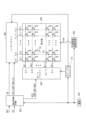
図1は、本実施形態における単位回路4の構成(シフトレジスタ410の一段分の構成)を示す回路図である。図1に示すように、この単位回路4は、4個の薄膜トランジスタT1~T4と2個のキャパシタ(容量素子)C1,C2とを備えている。薄膜トランジスタT1~T4は、nチャネル型のIGZO-TFTである。また、この単位回路4は、ローレベルの直流電源電圧VSS用の入力端子およびハイレベルの直流電源電圧VDD用の入力端子のほか、3個の入力端子41~43と、1個の出力端子49とを有している。ここで、セット信号Sを受け取る入力端子には符号41を付し、リセット信号Rを受け取る入力端子には符号42を付し、入力クロック信号CLKinを受け取る入力端子には符号43を付している。また、出力信号Qを出力するための出力端子に符号49を付している。
<3.1 First Embodiment>
<3.1.1 Circuit configuration>
FIG. 1 is a circuit diagram showing the configuration of the unit circuit 4 (the configuration of one stage of the shift register 410) in this embodiment. As shown in FIG. 1, the
薄膜トランジスタT3の制御端子、薄膜トランジスタT4の第1導通端子、およびキャパシタC1の一端は、第1制御ノードNA1を介して互いに接続されている。薄膜トランジスタT1の第2導通端子、薄膜トランジスタT2の第1導通端子、薄膜トランジスタT4の第2導通端子、およびキャパシタC2の一端は、第2制御ノードNA2を介して互いに接続されている。 A control terminal of the thin film transistor T3, a first conduction terminal of the thin film transistor T4, and one end of the capacitor C1 are connected to each other via a first control node NA1. A second conduction terminal of the thin film transistor T1, a first conduction terminal of the thin film transistor T2, a second conduction terminal of the thin film transistor T4, and one end of the capacitor C2 are connected to each other via a second control node NA2.
薄膜トランジスタT1については、制御端子および第1導通端子は入力端子41に接続され(すなわち、ダイオード接続となっている)、第2導通端子は第2制御ノードNA2に接続されている。なお、薄膜トランジスタT1の第1導通端子は、ハイレベルの直流電源電圧VDD用の入力端子に接続されていても良い。薄膜トランジスタT2については、制御端子は入力端子42に接続され、第1導通端子は第2制御ノードNA2に接続され、第2導通端子はローレベルの直流電源電圧VSS用の入力端子に接続されている。薄膜トランジスタT3については、制御端子は第1制御ノードNA1に接続され、第1導通端子は入力端子43に接続され、第2導通端子は出力端子49に接続されている。薄膜トランジスタT4については、制御端子はハイレベルの直流電源電圧VDD用の入力端子に接続され、第1導通端子は第1制御ノードNA1に接続され、第2導通端子は第2制御ノードNA2に接続されている。
As for the thin film transistor T1, the control terminal and the first conduction terminal are connected to the input terminal 41 (that is, are diode-connected), and the second conduction terminal is connected to the second control node NA2. The first conductive terminal of the thin film transistor T1 may be connected to the input terminal for the high level DC power supply voltage VDD. As for the thin film transistor T2, the control terminal is connected to the
キャパシタC1については、一端は第1制御ノードNA1に接続され、他端は出力端子49に接続されている。キャパシタC2については、一端は第2制御ノードNA2に接続され、他端は出力端子49に接続されている。
The capacitor C1 has one end connected to the first control node NA1 and the other end connected to the
上記のような構成において、薄膜トランジスタT3のチャネル幅は、薄膜トランジスタT4のチャネル幅の10倍以上となっている。従って、薄膜トランジスタT3の駆動能力は薄膜トランジスタT4の駆動能力に比べて充分に高くなっている。 In the above configuration, the channel width of the thin film transistor T3 is ten times or more the channel width of the thin film transistor T4. Therefore, the driving capability of the thin film transistor T3 is sufficiently higher than that of the thin film transistor T4.
なお、本実施形態においては、薄膜トランジスタT1によってセットトランジスタが実現され、薄膜トランジスタT2によってリセットトランジスタが実現され、薄膜トランジスタT3によって第1の出力制御トランジスタが実現され、薄膜トランジスタT4によって分離トランジスタが実現され、キャパシタC1によって第1キャパシタが実現され、キャパシタC2によって第2キャパシタが実現され、出力端子49によって第1出力ノードが実現されている。
In this embodiment, the thin film transistor T1 implements a set transistor, the thin film transistor T2 implements a reset transistor, the thin film transistor T3 implements a first output control transistor, the thin film transistor T4 implements an isolation transistor, and the capacitor C1. A first capacitor is realized by the capacitor C2, a second capacitor is realized by the capacitor C2, and the
<3.1.2 動作>
図6を参照しつつ、本実施形態における単位回路4の動作について説明する。時刻t11よりも前の期間には、第1制御ノードNA1の電位、第2制御ノードNA2の電位、および出力信号Qの電位(出力端子49の電位)はローレベル(オフレベル)である。なお、時刻t11よりも前の期間には、薄膜トランジスタT4はオン状態で維持されている。
<3.1.2 Operation>
The operation of the
時刻t11になると、セット信号Sがローレベルからハイレベル(オンレベル)に変化する。薄膜トランジスタT1は図1に示すようにダイオード接続となっているので、セット信号Sがハイレベルに変化することによって薄膜トランジスタT1はオン状態となり、キャパシタC2が充電される。これにより、第2制御ノードNA2の電位はローレベルからハイレベルに変化する。このとき薄膜トランジスタT4はオン状態であるので、キャパシタC1が充電され、第1制御ノードNA1の電位もローレベルからハイレベルに変化する。これにより、薄膜トランジスタT3がオン状態となる。ここで、時刻t11~時刻t12の期間中、入力クロック信号CLKinはローレベルで維持されている。このため、この期間中、出力信号Qはローレベルで維持される。 At time t11, the set signal S changes from low level to high level (on level). Since the thin film transistor T1 is diode-connected as shown in FIG. 1, the change of the set signal S to a high level turns on the thin film transistor T1 and charges the capacitor C2. As a result, the potential of the second control node NA2 changes from low level to high level. At this time, since the thin film transistor T4 is in the ON state, the capacitor C1 is charged and the potential of the first control node NA1 also changes from low level to high level. As a result, the thin film transistor T3 is turned on. Here, the input clock signal CLKin is maintained at low level during the period from time t11 to time t12. Therefore, the output signal Q is maintained at a low level during this period.
時刻t12になると、セット信号Sがハイレベルからローレベルに変化する。これにより、薄膜トランジスタT1はオフ状態となる。また、時刻t12には、入力クロック信号CLKinがローレベルからハイレベルに変化する。このとき、薄膜トランジスタT3はオン状態であるので、入力端子43の電位の上昇とともに出力端子49の電位が上昇する。ここで、図1に示すように第1制御ノードNA1-出力端子49間にはキャパシタC1が設けられているので、出力端子49の電位の上昇とともに第1制御ノードNA1の電位も上昇する(第1制御ノードNA1がブースト状態となる)。その結果、薄膜トランジスタT3には大きな電圧が印加され、この出力端子49に接続されているゲートバスラインGLが選択状態となるのに充分なレベルにまで出力信号Qの電位が上昇する。また、図1に示すように第2制御ノードNA2-出力端子49間にはキャパシタC2が設けられているので、出力端子49の電位の上昇とともに第2制御ノードNA2の電位も上昇する(第2制御ノードNA2がブースト状態となる)。ところで、薄膜トランジスタT4については、第1制御ノードNA1の電位および第2制御ノードNA2の電位が上昇することによって制御端子-第1導通端子間の電圧および制御端子-第2導通端子間の電圧が閾値電圧以下になるとオフ状態となる。これにより、第1制御ノードNA1と第2制御ノードNA2とは電気的に切り離された状態となる。
At time t12, the set signal S changes from high level to low level. As a result, the thin film transistor T1 is turned off. Also, at time t12, the input clock signal CLKin changes from low level to high level. At this time, since the thin film transistor T3 is on, the potential of the
時刻t13になると、入力クロック信号CLKinがハイレベルからローレベルに変化する。これにより、入力端子43の電位の低下とともに出力端子49の電位が低下する。すなわち、出力信号Qの電位がローレベルとなる。また、キャパシタC1を介して第1制御ノードNA1の電位が低下し、キャパシタC2を介して第2制御ノードNA2の電位が低下する。
At time t13, the input clock signal CLKin changes from high level to low level. As a result, the potential of the
時刻t14になると、リセット信号Rがローレベルからハイレベルに変化する。これにより、薄膜トランジスタT2がオン状態となり、第2制御ノードNA2の電位がローレベルとなる。また、薄膜トランジスタT4の制御端子-第2導通端子間の電圧が閾値電圧よりも大きくなり、薄膜トランジスタT4がオン状態となる。これにより、第1制御ノードNA1の電位もローレベルとなる。 At time t14, the reset signal R changes from low level to high level. As a result, the thin film transistor T2 is turned on, and the potential of the second control node NA2 becomes low level. Also, the voltage between the control terminal and the second conduction terminal of the thin film transistor T4 becomes higher than the threshold voltage, and the thin film transistor T4 is turned on. As a result, the potential of the first control node NA1 also becomes low level.
<3.1.3 効果>
出力信号Qの電位(出力端子49の電位)をハイレベルからローレベルへと変化させる動作に関し、薄膜トランジスタT3の放電能力は、入力クロック信号CLKinがハイレベルからローレベルに変化する時点(図6の時刻t13)の直前における第1制御ノードNA1の電位に依存する。第1制御ノードNA1の電位が充分に高ければ、入力クロック信号CLKinのハイレベルからローレベルへの変化に応じて出力信号Qの電位は速やかにハイレベルからローレベルへと変化する。
<3.1.3 Effects>
Regarding the operation of changing the potential of the output signal Q (the potential of the output terminal 49) from high level to low level, the discharge capability of the thin film transistor T3 is determined at the time when the input clock signal CLKin changes from high level to low level (see FIG. 6). It depends on the potential of the first control node NA1 immediately before time t13). If the potential of the first control node NA1 is sufficiently high, the potential of the output signal Q rapidly changes from high level to low level in accordance with the change of the input clock signal CLKin from high level to low level.
図15に示した従来の構成においては、薄膜トランジスタT91あるいは薄膜トランジスタT92でリーク電流が生じると、図17に示したように、入力クロック信号CLKinがハイレベルからローレベルに変化する時点(時刻t93)の直前には制御ノードNAの電位が所望の電位から顕著に低下している。それ故、薄膜トランジスタT3の放電能力の低下により出力信号Qの電位(出力端子49の電位)は緩やかに低下する。これにより、動作異常が発生する。 In the conventional configuration shown in FIG. 15, when a leakage current occurs in the thin film transistor T91 or the thin film transistor T92, as shown in FIG. Immediately before, the potential of the control node NA is remarkably lowered from the desired potential. Therefore, the potential of the output signal Q (the potential of the output terminal 49) gradually decreases due to the decrease in the discharge capability of the thin film transistor T3. This causes an operational anomaly.
これに対して、本実施形態によれば、図18に示した従来の構成と同様に単位回路4には制御ノード(単位回路4からの出力を制御するノード)を出力側の第1制御ノードNA1と入力側の第2制御ノードNA2とに分離する薄膜トランジスタT4が設けられているが、単位回路4には更に一端が第2制御ノードNA2に接続され他端が出力端子49に接続されたキャパシタC2が設けられている。このようにキャパシタC2が設けられているので、出力信号Qの電位(出力端子49の電位)の上昇に伴って第2制御ノードNA2の電位が上昇する。ここで、薄膜トランジスタT1の特性がエンハンスト型の特性からデプレッション型の特性へと変化することによる当該薄膜トランジスタT1でのリーク電流あるいは薄膜トランジスタT2の特性がエンハンスト型の特性からデプレッション型の特性へと変化することによる当該薄膜トランジスタT2でのリーク電流が生じて図6における時刻t12~時刻t13の期間中に第2制御ノードNA2の電位が低下しても、第2制御ノードNA2の電位が「VDD-Vth」(Vthは薄膜トランジスタT4の閾値電圧である)よりも高い限り薄膜トランジスタT4はオフ状態で維持される。また、上述のようにキャパシタC2が設けられているので、リーク電流が生じても、キャパシタC2が設けられていない構成に比べて第2制御ノードNA2の電位は緩やかに低下する。以上より、図7で符号70を付した部分に示すように、入力クロック信号CLKinがハイレベルからローレベルに変化する時点(時刻t13)の直前には第1制御ノードNA1の電位は充分に高いレベルで維持されている。それ故、図7で符号71を付した部分に示すように、入力クロック信号CLKinのハイレベルからローレベルへの変化に応じて出力信号Qの電位は速やかに低下する。また、薄膜トランジスタT4がオフ状態からオン状態へと変化しても、上述したように薄膜トランジスタT3のチャネル幅が薄膜トランジスタT4のチャネル幅の10倍以上となっていて薄膜トランジスタT3の駆動能力が薄膜トランジスタT4の駆動能力に比べて充分に高くなっているので、第2制御ノードNA2の電位の低下に応じて第1制御ノードNA1の電位が顕著に低下する前に出力信号Qの電位は充分に低下する。なお、出力信号Qの電位が充分に低下した後には第1制御ノードNA1の電位が低下しても問題は生じない。
In contrast, according to the present embodiment, in the
以上のように、本実施形態によれば、制御ノードに導通端子(第1導通端子または第2導通端子)(ドレインまたはソース)が接続された薄膜トランジスタT1,T2でのリーク電流に起因する動作異常の発生を抑制することのできるシフトレジスタ410が実現される。
As described above, according to the present embodiment, the operation abnormality caused by the leakage current in the thin film transistors T1 and T2 having the conduction terminal (first conduction terminal or second conduction terminal) (drain or source) connected to the control node
<3.2 第2の実施形態>
<3.2.1 回路構成>
図8は、本実施形態における単位回路4の構成(シフトレジスタ410の一段分の構成)を示す回路図である。第1の実施形態と同様、この単位回路4は、4個の薄膜トランジスタT1~T4と2個のキャパシタ(容量素子)C1,C2とを備えている。第1の実施形態においてはキャパシタC2の他端は出力端子49に接続されていたが、本実施形態においてはキャパシタC2の他端はローレベルの直流電源電圧VSS用の入力端子に接続されている。それ以外の点については、第1の実施形態と同様である。
<3.2 Second Embodiment>
<3.2.1 Circuit configuration>
FIG. 8 is a circuit diagram showing the configuration of the unit circuit 4 (the configuration for one stage of the shift register 410) in this embodiment. As in the first embodiment, this
<3.2.2 動作>
図9を参照しつつ、本実施形態における単位回路4の動作について説明する。時刻t21よりも前の期間には、第1制御ノードNA1の電位、第2制御ノードNA2の電位、および出力信号Qの電位(出力端子49の電位)はローレベルである。なお、時刻t11よりも前の期間には、薄膜トランジスタT4はオン状態で維持されている。
<3.2.2 Operation>
The operation of the
時刻t21になると、セット信号Sがローレベルからハイレベルに変化する。薄膜トランジスタT1は図8に示すようにダイオード接続となっているので、セット信号Sがハイレベルに変化することによって薄膜トランジスタT1はオン状態となり、キャパシタC2が充電される。これにより、第2制御ノードNA2の電位はローレベルからハイレベルに変化する。このとき薄膜トランジスタT4はオン状態であるので、キャパシタC1が充電され、第1制御ノードNA1の電位もローレベルからハイレベルに変化する。これにより、薄膜トランジスタT3がオン状態となる。ここで、時刻t21~時刻t22の期間中、入力クロック信号CLKinはローレベルで維持されている。このため、この期間中、出力信号Qはローレベルで維持される。 At time t21, the set signal S changes from low level to high level. Since the thin film transistor T1 is diode-connected as shown in FIG. 8, the change of the set signal S to a high level turns on the thin film transistor T1 and charges the capacitor C2. As a result, the potential of the second control node NA2 changes from low level to high level. At this time, since the thin film transistor T4 is in the ON state, the capacitor C1 is charged and the potential of the first control node NA1 also changes from low level to high level. As a result, the thin film transistor T3 is turned on. Here, during the period from time t21 to time t22, the input clock signal CLKin is maintained at low level. Therefore, the output signal Q is maintained at a low level during this period.
時刻t22になると、セット信号Sがハイレベルからローレベルに変化する。これにより、薄膜トランジスタT1はオフ状態となる。また、時刻t22には、入力クロック信号CLKinがローレベルからハイレベルに変化する。このとき、薄膜トランジスタT3はオン状態であるので、入力端子43の電位の上昇とともに出力端子49の電位が上昇する。ここで、図8に示すように第1制御ノードNA1-出力端子49間にはキャパシタC1が設けられているので、出力端子49の電位の上昇とともに第1制御ノードNA1の電位も上昇する(第1制御ノードNA1がブースト状態となる)。その結果、薄膜トランジスタT3には大きな電圧が印加され、この出力端子49に接続されているゲートバスラインGLが選択状態となるのに充分なレベルにまで出力信号Qの電位が上昇する。ところで、薄膜トランジスタT4の制御端子にはハイレベルの直流電源電圧VDDが与えられているので、時刻t21-時刻t22の期間に第1制御ノードNA1の電位および第2制御ノードNA2の電位が上昇することによって、時刻t22には薄膜トランジスタT4はオフ状態となっている(但し、薄膜トランジスタT4の閾値電圧によっては時刻t22以降に薄膜トランジスタT4がオフ状態となるケースもある)。従って、時刻t22以降に第1制御ノードNA1の電位が上昇しても第2制御ノードNA2の電位は上昇しない。
At time t22, the set signal S changes from high level to low level. As a result, the thin film transistor T1 is turned off. Also, at time t22, the input clock signal CLKin changes from low level to high level. At this time, since the thin film transistor T3 is on, the potential of the
時刻t23になると、入力クロック信号CLKinがハイレベルからローレベルに変化する。これにより、入力端子43の電位の低下とともに出力端子49の電位が低下する。すなわち、出力信号Qの電位がローレベルとなる。また、キャパシタC1を介して第1制御ノードNA1の電位が低下する。
At time t23, the input clock signal CLKin changes from high level to low level. As a result, the potential of the
時刻t24になると、リセット信号Rがローレベルからハイレベルに変化する。これにより、薄膜トランジスタT2がオン状態となり、第2制御ノードNA2の電位がローレベルとなる。また、薄膜トランジスタT4の制御端子-第2導通端子間の電圧が閾値電圧よりも大きくなり、薄膜トランジスタT4がオン状態となる。これにより、第1制御ノードNA1の電位もローレベルとなる。 At time t24, the reset signal R changes from low level to high level. As a result, the thin film transistor T2 is turned on, and the potential of the second control node NA2 becomes low level. Also, the voltage between the control terminal and the second conduction terminal of the thin film transistor T4 becomes higher than the threshold voltage, and the thin film transistor T4 is turned on. As a result, the potential of the first control node NA1 also becomes low level.
<3.2.3 効果>
本実施形態によれば、薄膜トランジスタT1あるいは薄膜トランジスタT2でのリーク電流に起因して図9の時刻t22~時刻t23の期間中に第2制御ノードNA2の電位が低下すると、当該期間中に第1制御ノードNA1の電位も低下する。しかしながら、単位回路4には一端が第2制御ノードNA2に接続されたキャパシタC2が設けられているので、リーク電流が生じても、キャパシタC2が設けられていない構成に比べて第2制御ノードNA2の電位は緩やかに低下する。例えば、キャパシタC2が設けられていない構成においては図10で実線で示す波形のように第2制御ノードNA2の電位が低下するのに対して、キャパシタC2が設けられている構成(本実施形態の構成)においては図10で太点線で示す波形のように第2制御ノードNA2の電位が低下する。従って、本実施形態においては、リーク電流が生じたときに第1制御ノードNA1の電位は緩やかに低下し、薄膜トランジスタT3の放電能力の低下が抑制される。以上のように、本実施形態によれば、キャパシタC2が設けられていない構成に比べて、制御ノード(単位回路4からの出力を制御するノード)に導通端子(第1導通端子または第2導通端子)(ドレインまたはソース)が接続された薄膜トランジスタT1,T2でのリーク電流に起因する動作異常の発生が抑制される。
<3.2.3 Effects>
According to this embodiment, when the potential of the second control node NA2 drops during the period from time t22 to time t23 in FIG. The potential of node NA1 also drops. However, since the
また、本実施形態によれば、図9の時刻t22に第1制御ノードNA1がブースト状態となっても第2制御ノードNA2の電位は時刻t22の直前の電位で維持される。それ故、薄膜トランジスタT1,T2の第1導通端子-第2導通端子間(ドレイン-ソース間)に高電圧が印加されることが抑制される。これにより、薄膜トランジスタT1,T2の劣化や破壊に起因する動作異常の発生が抑制される。 Further, according to the present embodiment, even if the first control node NA1 enters the boost state at time t22 in FIG. 9, the potential of the second control node NA2 is maintained at the potential immediately before time t22. Therefore, application of a high voltage between the first conduction terminal and the second conduction terminal (between the drain and the source) of the thin film transistors T1 and T2 is suppressed. This suppresses the occurrence of abnormal operation due to deterioration or destruction of the thin film transistors T1 and T2.
<4.実際的な回路への適用例>
第1の実施形態および第2の実施形態として示した単位回路4は、基本的な構成を有する単位回路である。しかしながら実際の表示装置には様々な構成の単位回路が採用されており、本明細書での開示内容はそのような様々な構成の単位回路に適用することができる。そこで、実際的な回路への適用例として2つの例(第1の例および第2の例)を以下に説明する。
<4. Example of application to a practical circuit>
The
<4.1 第1の例>
ゲートドライバ400内のシフトレジスタ410を構成する単位回路4には、動作の安定化のための回路(以下、「安定化回路」という。)が設けられていることが多い。安定化回路の構成としては様々な構成が考えられているが、ここでは安定化回路を含む単位回路の一構成例を第1の例として説明する。
<4.1 First example>
The
図11は、第1の例における単位回路4の構成(シフトレジスタ410の一段分の構成)を示す回路図である。図11に示すように、この単位回路4は、8個の薄膜トランジスタT1~T8と2個のキャパシタ(容量素子)C1,C2とを備えている。また、この単位回路は、ローレベルの直流電源電圧VSS用の入力端子およびハイレベルの直流電源電圧VDD用の入力端子のほか、3個の入力端子41~43と、1個の出力端子49とを有している。薄膜トランジスタT5の制御端子、薄膜トランジスタT6の第2導通端子、薄膜トランジスタT7の第1導通端子、および薄膜トランジスタT8の第1導通端子は、安定化ノードNBを介して互いに接続されている。
FIG. 11 is a circuit diagram showing the configuration of the unit circuit 4 (the configuration for one stage of the shift register 410) in the first example. As shown in FIG. 11, this
薄膜トランジスタT1~T4およびキャパシタC1,C2の構成については第1の実施形態と同様である。但し、第2の実施形態(図8参照)と同様にキャパシタC2の他端がローレベルの直流電源電圧VSS用の入力端子に接続されていても良い。薄膜トランジスタT5については、制御端子は安定化ノードNBに接続され、第1導通端子は第2制御ノードNA2に接続され、第2導通端子はローレベルの直流電源電圧VSS用の入力端子に接続されている。薄膜トランジスタT6については、制御端子および第1導通端子はハイレベルの直流電源電圧VDD用の入力端子に接続され(すなわち、ダイオード接続となっている)、第2導通端子は安定化ノードNBに接続されている。薄膜トランジスタT7については、制御端子は第1制御ノードNA1に接続され、第1導通端子は安定化ノードNBに接続され、第2導通端子はローレベルの直流電源電圧VSS用の入力端子に接続されている。薄膜トランジスタT8については、制御端子は入力端子41に接続され、第1導通端子は安定化ノードNBに接続され、第2導通端子はローレベルの直流電源電圧VSS用の入力端子に接続されている。なお、薄膜トランジスタT5~T8と安定化ノードNBとによって安定化回路46が実現されている。また、薄膜トランジスタT5によって、安定化トランジスタが実現されている。
The configurations of thin film transistors T1 to T4 and capacitors C1 and C2 are the same as in the first embodiment. However, as in the second embodiment (see FIG. 8), the other end of the capacitor C2 may be connected to the input terminal for the low-level DC power supply voltage VSS. As for the thin film transistor T5, the control terminal is connected to the stabilization node NB, the first conduction terminal is connected to the second control node NA2, and the second conduction terminal is connected to the input terminal for the low level DC power supply voltage VSS. there is As for the thin film transistor T6, the control terminal and the first conduction terminal are connected to the input terminal for the high level DC power supply voltage VDD (that is, are diode-connected), and the second conduction terminal is connected to the stabilization node NB. ing. As for the thin film transistor T7, the control terminal is connected to the first control node NA1, the first conduction terminal is connected to the stabilization node NB, and the second conduction terminal is connected to the input terminal for the low level DC power supply voltage VSS. there is As for the thin film transistor T8, the control terminal is connected to the
以上のような構成によれば、図12に示すように、第1制御ノードNA1の電位がローレベルで維持されるべき期間には安定化ノードNBの電位はハイレベルで維持され、第1制御ノードNA1の電位がハイレベルで維持されるべき期間には安定化ノードNBの電位はローレベルで維持される。これにより、図12における時刻t31よりも前の期間および時刻t34よりも後の期間には、薄膜トランジスタT5がオン状態で維持されことによって第2制御ノードNA2の電位が確実にローレベルで維持される。このようにして、単位回路4の動作異常の発生が抑制される。
According to the above configuration, as shown in FIG. 12, the potential of the stabilization node NB is maintained at a high level while the potential of the first control node NA1 is to be maintained at a low level. The potential of the stabilization node NB is maintained at low level during the period when the potential of node NA1 should be maintained at high level. As a result, during the period before time t31 and the period after time t34 in FIG. 12, the thin film transistor T5 is maintained in the ON state, thereby reliably maintaining the potential of the second control node NA2 at the low level. . In this manner, occurrence of malfunction of the
<4.2 第2の例>
第1の実施形態および第2の実施形態においては、各単位回路4から出力される出力信号Qは、対応するゲートバスラインGLに走査信号Gとして与えられるほか、リセット信号Rとして3段前の単位回路4に与えられるとともにセット信号Sとして2段後の単位回路4に与えられる。このような構成によれば、ゲートバスラインGLの負荷容量が顕著に大きい場合にリセット信号Rやセット信号Sに波形の鈍りが生じることによって単位回路4の動作に異常が生じることが懸念される。そこで、そのような異常の発生が抑制されるよう走査信号Gとなる出力信号とセット信号Sおよびリセット信号Rとなる出力信号とが異なる出力端子から出力されるようにした構成を第2の例として説明する。
<4.2 Second example>
In the first and second embodiments, the output signal Q output from each
図13は、第2の例における単位回路4からの出力信号について説明するための図である。図13に示すように、単位回路4からは出力信号として第1出力信号Q1と第2出力信号Q2とが出力される。n段目の単位回路4(n)出力される第1出力信号Q1は、走査信号G(n)としてゲートバスラインGLnに与えられる。n段目以外の単位回路4から出力される第1出力信号Q1についても同様である。n段目の単位回路4(n)出力される第2出力信号Q2は、リセット信号Rとして3段前の単位回路4(n-3)に与えられるとともにセット信号Sとして2段後の単位回路4(n+2)に与えられる。n段目以外の単位回路4から出力される第2出力信号Q2についても同様である。
FIG. 13 is a diagram for explaining output signals from the
図14は、第2の例における単位回路4の構成(シフトレジスタ410の一段分の構成)を示す回路図である。図14に示すように、この単位回路4は、5個の薄膜トランジスタT1~T4,T9と2個のキャパシタ(容量素子)C1,C2とを備えている。また、この単位回路は、ローレベルの直流電源電圧VSS用の入力端子およびハイレベルの直流電源電圧VDD用の入力端子のほか、3個の入力端子41~43と、2個の出力端子491,492とを有している。出力端子491からは第1出力信号Q1が出力される。出力端子492からは第2出力信号Q2が出力される。
FIG. 14 is a circuit diagram showing the configuration of the unit circuit 4 (the configuration for one stage of the shift register 410) in the second example. As shown in FIG. 14, the
薄膜トランジスタT3については、制御端子は第1制御ノードNA1に接続され、第1導通端子は入力端子43に接続され、第2導通端子は出力端子491に接続されている。薄膜トランジスタT9については、制御端子は第1制御ノードNA1に接続され、第1導通端子は入力端子43に接続され、第2導通端子は出力端子492に接続されている。キャパシタC1については、一端は第1制御ノードNA1に接続され、他端は出力端子491に接続されている。キャパシタC2については、一端は第2制御ノードNA2に接続され、他端は出力端子491に接続されている。それ以外の点については、第1の実施形態と同様である。なお、第2の実施形態(図8参照)と同様にキャパシタC2の他端がローレベルの直流電源電圧VSS用の入力端子に接続されていても良い。
As for the thin film transistor T3, the control terminal is connected to the first control node NA1, the first conduction terminal is connected to the
この第2の例においては、薄膜トランジスタT9によって第2の出力制御トランジスタが実現され、出力端子491によって第1出力ノードが実現され、出力端子492によって第2出力ノードが実現されている。
In this second example, the thin film transistor T9 implements the second output control transistor, the
以上のような第2の例によれば、ゲートバスラインGLの負荷容量が顕著に大きい場合であっても、各単位回路4においてセット信号Sに基づく動作およびリセット信号Rに基づく動作が速やかに行われ、回路動作の安定性が向上する。
According to the second example as described above, even when the load capacitance of the gate bus line GL is remarkably large, the operation based on the set signal S and the operation based on the reset signal R are performed quickly in each
<5.その他>
以上において本発明を詳細に説明したが、以上の説明は全ての面で例示的なものであって制限的なものではない。多数の他の変更や変形が本発明の範囲を逸脱することなく案出可能であると了解される。例えば、上記の説明では液晶表示装置を例に挙げたが、複数のゲートバスライン(走査信号線)を順次に駆動する表示装置であれば液晶表示装置以外の表示装置(例えば、有機EL表示装置)にも上記開示内容を適用することができる。
<5. Others>
Although the present invention has been described in detail above, the above description is illustrative in all respects and is not restrictive. It will be appreciated that numerous other modifications and variations can be devised without departing from the scope of the invention. For example, in the above description, a liquid crystal display device was taken as an example, but a display device other than a liquid crystal display device (for example, an organic EL display device) can be used as long as it is a display device that sequentially drives a plurality of gate bus lines (scanning signal lines). ) can also be applied to the above disclosure.
4…単位回路
400…ゲートドライバ
410…シフトレジスタ
600…表示部
T1~T9…薄膜トランジスタ(TFT)
C1,C2…キャパシタ
NA1…第1制御ノード
NA2…第2制御ノード
GL、GL1~GLi…ゲートバスライン(走査信号線)
G、G(1)~G(i)…走査信号
CLKin…入力クロック信号
GCK…ゲートクロック信号
S…セット信号
R…リセット信号
4
C1, C2...Capacitor NA1...First control node NA2...Second control node GL, GL1 to GLi...Gate bus lines (scanning signal lines)
G, G(1) to G(i)...scanning signal CLKin...input clock signal GCK...gate clock signal S...set signal R...reset signal
Claims (10)
各段を構成する単位回路は、
第1出力ノードと、
第1制御ノードと、
第2制御ノードと、
前記第1制御ノードに接続された制御端子と、前記複数のクロック信号の1つである入力クロック信号が与えられる第1導通端子と、前記第1出力ノードに接続された第2導通端子とを有する第1の出力制御トランジスタと、
先行する段を構成する単位回路から出力される出力信号であるセット信号が与えられる制御端子と、前記セット信号またはオンレベルの電位が与えられる第1導通端子と、前記第2制御ノードに接続された第2導通端子とを有するセットトランジスタと、
後続の段を構成する単位回路から出力される出力信号であるリセット信号が与えられる制御端子と、前記第2制御ノードに接続された第1導通端子と、オフレベルの電位が与えられる第2導通端子とを有するリセットトランジスタと、
オンレベルの電位が与えられる制御端子と、前記第1制御ノードに接続された第1導通端子と、前記第2制御ノードに接続された第2導通端子とを有する分離トランジスタと、
一端が前記第1制御ノードに接続され、他端が前記第1出力ノードに接続された第1キャパシタと、
一端が前記第2制御ノードに接続された第2キャパシタと
を含むことを特徴とする、シフトレジスタ。 A shift register consisting of a plurality of stages that operates based on a plurality of clock signals,
The unit circuit that constitutes each stage is
a first output node;
a first control node;
a second control node;
a control terminal connected to the first control node; a first conduction terminal to which an input clock signal that is one of the plurality of clock signals is applied; and a second conduction terminal connected to the first output node. a first output control transistor having
A control terminal supplied with a set signal, which is an output signal output from a unit circuit constituting the preceding stage, a first conduction terminal supplied with the set signal or an on-level potential, and the second control node. a set transistor having a second conduction terminal;
A control terminal to which a reset signal, which is an output signal output from a unit circuit forming a succeeding stage, is applied, a first conduction terminal connected to the second control node, and a second conduction terminal to which an off-level potential is applied. a reset transistor having a terminal;
an isolation transistor having a control terminal to which an on-level potential is applied, a first conduction terminal connected to the first control node, and a second conduction terminal connected to the second control node;
a first capacitor having one end connected to the first control node and the other end connected to the first output node;
and a second capacitor having one end connected to the second control node.
前記第1制御ノードの電位がオフレベルで維持されるべき期間には、前記安定化ノードの電位はオンレベルで維持され、
前記第1制御ノードの電位がオンレベルで維持されるべき期間には、前記安定化ノードの電位はオフレベルで維持されることを特徴とする、請求項1から4までのいずれか1項に記載のシフトレジスタ。 The unit circuit further includes a stabilization node, a control terminal connected to the stabilization node, a first conduction terminal connected to the second control node, and a second conduction terminal supplied with an off-level potential. a stabilization circuit for controlling the potential of the second control node, comprising a stabilization transistor having
During a period in which the potential of the first control node should be maintained at the off level, the potential of the stabilization node is maintained at the on level,
5. The method according to any one of claims 1 to 4, characterized in that the potential of the stabilization node is maintained at the off level during a period in which the potential of the first control node is to be maintained at the on level. A shift register as described.
第2出力ノードと、
前記第1制御ノードに接続された制御端子と、前記入力クロック信号が与えられる第1導通端子と、前記第2出力ノードに接続された第2導通端子とを有する第2の出力制御トランジスタと
を更に含み、
前記第2出力ノードから出力される出力信号は、先行する段を構成する単位回路に前記リセット信号として与えられるとともに後続の段を構成する単位回路に前記セット信号として与えられることを特徴とする、請求項1から5までのいずれか1項に記載のシフトレジスタ。 The unit circuit is
a second output node;
a second output control transistor having a control terminal connected to the first control node, a first conduction terminal to which the input clock signal is applied, and a second conduction terminal connected to the second output node; further includes
The output signal output from the second output node is provided as the reset signal to the unit circuit forming the preceding stage and is provided as the set signal to the unit circuit forming the succeeding stage, Shift register according to any one of claims 1 to 5.
請求項1から8までのいずれか1項に記載のシフトレジスタを備え、
前記複数の走査信号線と1対1で対応するように、前記複数の段を構成する複数の単位回路が設けられ、
各単位回路に含まれる前記第1出力ノードは、対応する走査信号線に接続されていることを特徴とする、走査信号線駆動回路。 A scanning signal line driving circuit for driving a plurality of scanning signal lines arranged in a display section for displaying an image,
A shift register according to any one of claims 1 to 8,
a plurality of unit circuits constituting the plurality of stages are provided so as to correspond to the plurality of scanning signal lines on a one-to-one basis;
A scanning signal line driving circuit, wherein the first output node included in each unit circuit is connected to a corresponding scanning signal line.
Priority Applications (2)
| Application Number | Priority Date | Filing Date | Title |
|---|---|---|---|
| JP2021211880A JP2023096258A (en) | 2021-12-27 | 2021-12-27 | Shift register and scan signal line driving circuit and display including the same |
| US18/075,307 US11955097B2 (en) | 2021-12-27 | 2022-12-05 | Shift register, scanning signal line driving circuit including same, and display device including same |
Applications Claiming Priority (1)
| Application Number | Priority Date | Filing Date | Title |
|---|---|---|---|
| JP2021211880A JP2023096258A (en) | 2021-12-27 | 2021-12-27 | Shift register and scan signal line driving circuit and display including the same |
Publications (1)
| Publication Number | Publication Date |
|---|---|
| JP2023096258A true JP2023096258A (en) | 2023-07-07 |
Family
ID=86897038
Family Applications (1)
| Application Number | Title | Priority Date | Filing Date |
|---|---|---|---|
| JP2021211880A Pending JP2023096258A (en) | 2021-12-27 | 2021-12-27 | Shift register and scan signal line driving circuit and display including the same |
Country Status (2)
| Country | Link |
|---|---|
| US (1) | US11955097B2 (en) |
| JP (1) | JP2023096258A (en) |
Family Cites Families (15)
| Publication number | Priority date | Publication date | Assignee | Title |
|---|---|---|---|---|
| WO2011055569A1 (en) | 2009-11-04 | 2011-05-12 | シャープ株式会社 | Shift register and the scan signal line driving circuit provided there with, and display device |
| KR101097347B1 (en) * | 2010-03-11 | 2011-12-21 | 삼성모바일디스플레이주식회사 | A gate driving circuit and a display apparatus using the same |
| WO2011114562A1 (en) * | 2010-03-15 | 2011-09-22 | シャープ株式会社 | Scan signal line drive circuit and display device provided therewith |
| JP5396543B2 (en) * | 2010-09-02 | 2014-01-22 | シャープ株式会社 | Signal processing circuit, driver circuit, display device |
| JPWO2012029874A1 (en) * | 2010-09-02 | 2013-10-31 | シャープ株式会社 | Signal processing circuit, inverter circuit, buffer circuit, driver circuit, level shifter, display device |
| CN106098002B (en) * | 2016-08-05 | 2018-10-19 | 武汉华星光电技术有限公司 | Scan drive circuit and flat display apparatus with the circuit |
| CN107146570A (en) * | 2017-07-17 | 2017-09-08 | 京东方科技集团股份有限公司 | Shift register cell, scan drive circuit, array base palte and display device |
| KR102367271B1 (en) * | 2017-07-28 | 2022-02-23 | 엘지디스플레이 주식회사 | Gate driving circuit and display device using the same |
| CN110176217B (en) * | 2018-07-16 | 2020-06-23 | 京东方科技集团股份有限公司 | Shifting register unit and driving method thereof, grid driving circuit and display device |
| US10964244B2 (en) * | 2018-09-04 | 2021-03-30 | Sharp Kabushiki Kaisha | Display device |
| US10825414B2 (en) | 2018-10-26 | 2020-11-03 | Sharp Kabushiki Kaisha | Scanning signal line drive circuit, display device provided with same, and drive method for scanning signal line |
| KR20220042031A (en) * | 2020-09-25 | 2022-04-04 | 삼성디스플레이 주식회사 | Gate driving circuit and display apparatus including the same |
| US11450257B2 (en) * | 2020-11-27 | 2022-09-20 | Lg Display Co., Ltd. | Gate driving circuit and electroluminescence display apparatus including the same |
| US11854458B2 (en) * | 2021-04-27 | 2023-12-26 | Chengdu Boe Optoelectronics Technology Co., Ltd. | Driving circuit connecting first control voltage terminal and second voltage control terminal, driving method, shift register and display device |
| KR20230103629A (en) * | 2021-12-31 | 2023-07-07 | 엘지디스플레이 주식회사 | Gate driving circuit and display device including the same |
-
2021
- 2021-12-27 JP JP2021211880A patent/JP2023096258A/en active Pending
-
2022
- 2022-12-05 US US18/075,307 patent/US11955097B2/en active Active
Also Published As
| Publication number | Publication date |
|---|---|
| US11955097B2 (en) | 2024-04-09 |
| US20230206875A1 (en) | 2023-06-29 |
Similar Documents
| Publication | Publication Date | Title |
|---|---|---|
| JP5535374B2 (en) | Scanning signal line driving circuit and display device including the same | |
| EP2357642B1 (en) | Scanning signal line driving circuit and shift register | |
| JP5165153B2 (en) | Scanning signal line driving circuit, display device including the same, and scanning signal line driving method | |
| TWI529682B (en) | A scanning signal line driving circuit, a display device including the same, and a driving method of a scanning signal line | |
| JP5372268B2 (en) | Scanning signal line driving circuit, display device including the same, and scanning signal line driving method | |
| US10706803B2 (en) | Shift register circuit | |
| JP6033225B2 (en) | Display device and scanning signal line driving method | |
| US8605028B2 (en) | Scanning signal line drive circuit, shift register and display device | |
| WO2014092011A1 (en) | Display device and method for driving same | |
| WO2011129126A1 (en) | Scan signal line drive circuit and display device provided therewith | |
| JP5972267B2 (en) | Liquid crystal display device and driving method of auxiliary capacitance line | |
| JP6246976B2 (en) | Shift register circuit and display device having the same | |
| US11138947B2 (en) | Scanning signal line drive circuit and display device provided with same | |
| WO2018193912A1 (en) | Scanning signal line driving circuit and display device equipped with same | |
| CN110120202B (en) | Display device | |
| JP6316423B2 (en) | Shift register and display device including the same | |
| US10854163B2 (en) | Display device suppressing display failure caused by residual charge | |
| US10796659B2 (en) | Display device and method for driving the same | |
| CN109887469B (en) | Shift register and display device having the same | |
| JP2023096258A (en) | Shift register and scan signal line driving circuit and display including the same | |
| JP2023096257A (en) | Shift register and scan signal line driving circuit and display including the same |