WO2016203984A1 - 撮像装置および制御方法 - Google Patents
撮像装置および制御方法 Download PDFInfo
- Publication number
- WO2016203984A1 WO2016203984A1 PCT/JP2016/066543 JP2016066543W WO2016203984A1 WO 2016203984 A1 WO2016203984 A1 WO 2016203984A1 JP 2016066543 W JP2016066543 W JP 2016066543W WO 2016203984 A1 WO2016203984 A1 WO 2016203984A1
- Authority
- WO
- WIPO (PCT)
- Prior art keywords
- pixel
- imaging device
- light
- current value
- detection unit
- Prior art date
- Legal status (The legal status is an assumption and is not a legal conclusion. Google has not performed a legal analysis and makes no representation as to the accuracy of the status listed.)
- Ceased
Links
Images



Classifications
-
- H—ELECTRICITY
- H04—ELECTRIC COMMUNICATION TECHNIQUE
- H04N—PICTORIAL COMMUNICATION, e.g. TELEVISION
- H04N23/00—Cameras or camera modules comprising electronic image sensors; Control thereof
- H04N23/70—Circuitry for compensating brightness variation in the scene
- H04N23/72—Combination of two or more compensation controls
-
- H—ELECTRICITY
- H04—ELECTRIC COMMUNICATION TECHNIQUE
- H04N—PICTORIAL COMMUNICATION, e.g. TELEVISION
- H04N23/00—Cameras or camera modules comprising electronic image sensors; Control thereof
- H04N23/10—Cameras or camera modules comprising electronic image sensors; Control thereof for generating image signals from different wavelengths
- H04N23/11—Cameras or camera modules comprising electronic image sensors; Control thereof for generating image signals from different wavelengths for generating image signals from visible and infrared light wavelengths
-
- H—ELECTRICITY
- H04—ELECTRIC COMMUNICATION TECHNIQUE
- H04N—PICTORIAL COMMUNICATION, e.g. TELEVISION
- H04N23/00—Cameras or camera modules comprising electronic image sensors; Control thereof
- H04N23/10—Cameras or camera modules comprising electronic image sensors; Control thereof for generating image signals from different wavelengths
- H04N23/12—Cameras or camera modules comprising electronic image sensors; Control thereof for generating image signals from different wavelengths with one sensor only
-
- H—ELECTRICITY
- H04—ELECTRIC COMMUNICATION TECHNIQUE
- H04N—PICTORIAL COMMUNICATION, e.g. TELEVISION
- H04N23/00—Cameras or camera modules comprising electronic image sensors; Control thereof
- H04N23/60—Control of cameras or camera modules
- H04N23/65—Control of camera operation in relation to power supply
-
- H—ELECTRICITY
- H04—ELECTRIC COMMUNICATION TECHNIQUE
- H04N—PICTORIAL COMMUNICATION, e.g. TELEVISION
- H04N23/00—Cameras or camera modules comprising electronic image sensors; Control thereof
- H04N23/60—Control of cameras or camera modules
- H04N23/66—Remote control of cameras or camera parts, e.g. by remote control devices
- H04N23/661—Transmitting camera control signals through networks, e.g. control via the Internet
-
- H—ELECTRICITY
- H04—ELECTRIC COMMUNICATION TECHNIQUE
- H04N—PICTORIAL COMMUNICATION, e.g. TELEVISION
- H04N23/00—Cameras or camera modules comprising electronic image sensors; Control thereof
- H04N23/70—Circuitry for compensating brightness variation in the scene
- H04N23/71—Circuitry for evaluating the brightness variation
-
- H—ELECTRICITY
- H04—ELECTRIC COMMUNICATION TECHNIQUE
- H04N—PICTORIAL COMMUNICATION, e.g. TELEVISION
- H04N25/00—Circuitry of solid-state image sensors [SSIS]; Control thereof
- H04N25/70—SSIS architectures; Circuits associated therewith
Definitions
- the present disclosure relates to an imaging apparatus and a control method, and more particularly, to an imaging apparatus and a control method capable of realizing low power consumption.
- Patent Document 1 proposes a time synchronization information calculation method. In this proposal, synchronization is performed by converting an actually captured image. Is going.
- Patent Document 1 it is necessary to perform a shooting operation for synchronization, and it is difficult to realize low power consumption. Further, the image used for synchronization is difficult to use for the original photographing purpose, and is wasted.
- the present disclosure has been made in view of such a situation, and can realize low power consumption.
- An imaging device receives light from a light source, detects a change in the current value of the pixel by using photoelectric conversion, detects a change in the current value of the pixel, and outputs a detection result. And a detection unit that performs a corresponding operation instruction.
- the pixel is a pixel specialized in detecting the brightness of the shooting environment, and is a pixel that uses photoelectric conversion to convert the amount of received light into a current value without power consumption.
- the detection unit can detect at least one of light intensity, light reception time, blinking pattern, and wavelength as a change in the current value of the pixel.
- the detection unit can detect an instruction trigger composed of a combination of changes in the current value of the pixel.
- the detection unit can be composed of a combination of changes in the current value of the pixel, and can detect different indication triggers for each color.
- the detection unit is composed of a combination of changes in the current value of the pixel, and can detect indication triggers of different frequencies at the same time.
- the detection unit can issue a system activation instruction to each unit other than itself.
- the detection unit can instruct transmission of image data to another device.
- the detection unit can issue an imaging instruction to a solid-state imaging device including the pixels.
- the detection unit can instruct data transfer including a combination of changes in the current value of the pixel.
- an imaging device receives light from a light source, detects a change in a current value of a pixel that converts a received light amount into a current value using photoelectric conversion, and outputs a detection result.
- the corresponding operation instruction is given.
- light from a light source is received, and a change in the current value of a pixel that converts the amount of received light into a current value is detected using photoelectric conversion. Then, an operation instruction according to the detection result is performed.
- FIG. 2 It is a block diagram which shows the schematic structural example of the solid-state imaging device to which this technique is applied. It is a block diagram showing an example of an imaging system to which the present technology is applied. 3 is a flowchart for describing processing of the imaging system in FIG. 2. It is a block diagram showing an example of an imaging device to which this art is applied. It is a block diagram which shows the example of the imaging system containing the imaging device of FIG. 6 is a flowchart for describing processing of the imaging system in FIG. 5. It is a figure which shows the example of light source light emission. It is a figure which shows the example of an instruction
- FIG. 1 illustrates a schematic configuration example of an example of a complementary metal oxide semiconductor (CMOS) solid-state imaging device applied to each embodiment of the present technology.
- CMOS complementary metal oxide semiconductor
- a solid-state imaging device (element chip) 1 includes a pixel region (a pixel region in which pixels 2 including a plurality of photoelectric conversion elements are regularly arranged two-dimensionally on a semiconductor substrate 11 (for example, a silicon substrate). A so-called imaging region) 3 and a peripheral circuit section.
- the pixel 2 includes a photoelectric conversion element (for example, a photodiode) and a plurality of pixel transistors (so-called MOS transistors).
- the plurality of pixel transistors can be constituted by three transistors, for example, a transfer transistor, a reset transistor, and an amplifying transistor, and can further be constituted by four transistors by adding a selection transistor. Since the equivalent circuit of each pixel 2 (unit pixel) is the same as a general one, detailed description thereof is omitted here.
- the pixel 2 can have a shared pixel structure.
- the pixel sharing structure includes a plurality of photodiodes, a plurality of transfer transistors, one shared floating diffusion, and one other pixel transistor that is shared.
- the peripheral circuit section includes a vertical drive circuit 4, a column signal processing circuit 5, a horizontal drive circuit 6, an output circuit 7, and a control circuit 8.
- the control circuit 8 receives data for instructing an input clock, an operation mode, and the like, and outputs data such as internal information of the solid-state imaging device 1. Specifically, the control circuit 8 is based on the vertical synchronization signal, the horizontal synchronization signal, and the master clock, and the clock signal or the reference signal for the operations of the vertical drive circuit 4, the column signal processing circuit 5, and the horizontal drive circuit 6 Generate a control signal. The control circuit 8 inputs these signals to the vertical drive circuit 4, the column signal processing circuit 5, and the horizontal drive circuit 6.
- the vertical drive circuit 4 is composed of, for example, a shift register, selects a pixel drive wiring, supplies a pulse for driving the pixel 2 to the selected pixel drive wiring, and drives the pixels 2 in units of rows. Specifically, the vertical drive circuit 4 selectively scans each pixel 2 in the pixel region 3 sequentially in the vertical direction in units of rows, and generates the signal according to the amount of light received by the photoelectric conversion element of each pixel 2 through the vertical signal line 9. A pixel signal based on the signal charge is supplied to the column signal processing circuit 5.
- the column signal processing circuit 5 is disposed, for example, for each column of the pixels 2 and performs signal processing such as noise removal on the signal output from the pixels 2 for one row for each pixel column. Specifically, the column signal processing circuit 5 performs signal processing such as CDS (Correlated Double Sampling) for removing fixed pattern noise specific to the pixel 2, signal amplification, A / D (Analog / Digital) conversion, and the like. .
- a horizontal selection switch (not shown) is provided connected to the horizontal signal line 10.
- the horizontal drive circuit 6 is constituted by, for example, a shift register, and sequentially outputs horizontal scanning pulses to select each of the column signal processing circuits 5 in order, and the pixel signal is output from each of the column signal processing circuits 5 to the horizontal signal line. 10 to output.
- the output circuit 7 performs signal processing on the signals sequentially supplied from each of the column signal processing circuits 5 through the horizontal signal line 10 and outputs the signals.
- the output circuit 7 may perform only buffering, or may perform black level adjustment, column variation correction, various digital signal processing, and the like.
- the input / output terminal 12 is provided for exchanging signals with the outside.
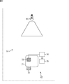
- FIG. 2 is a block diagram illustrating an example of an imaging system to which the present technology is applied.
- the 2 is configured to include, for example, a light source 61 and an imaging device 62.
- the imaging system 51 includes another imaging device 62 and other devices (not shown).
- the light source 61 is a light source having a wavelength that can be received by an OPD (optical detector) 73, which is a pixel that performs exposure detection, and the light emission is controlled by a PC (Personal Computer), which will be described later.
- OPD optical detector
- PC Personal Computer
- the imaging device 62 is configured to include a solid-state imaging device 71, a memory 72, an OPD pixel 73, a detector 74, and a control object 75.
- the imaging device 62 is normally in a stopped state (super low power consumption state) except for the detector 74.
- the solid-state imaging device 71 is basically the same as the solid-state imaging device 1 except that at least one of the pixels 2 is replaced with the OPD pixel 73.
- the arrangement of the OPD pixels 73 is not particularly limited as long as it is within the pixel region 3.
- the memory 72 is a fixed memory recorded at the time of production, and has an ID unique to the imaging device 62 built therein.
- the OPD pixel 73 is a pixel specialized in detecting the brightness of the shooting environment, and converts the amount of received light into a current value without photoelectric consumption using photoelectric conversion.
- the OPD pixel 73 is provided in advance for confirming and adjusting the photographing condition (exposure time).
- the OPD pixel 73 can have a wide dynamic range. If the OPD pixel 73 is not embedded, another pixel 2 can be used. In this case, the solid-state imaging device 71 needs to be activated.
- the detector 74 detects a change in the current value of the OPD pixel 73 (light intensity, light reception time, blinking pattern, etc.) because the current overflows in the OPD pixel 73, and if it detects it, the operation according to the detection result An instruction is given to the control object 75 and the solid-state imaging device 71.
- the control object 75 is an object for which the detection unit 74 gives (controls) an operation instruction based on the detection result from the detector 74.
- the target is, for example, another device (not shown) included in the imaging system 51 or each part of the imaging device 62. Note that when an operation instruction is given to another device, a function such as wireless communication is provided.
- the solid-state imaging device 71 may include the memory 72, the OPD pixel 73, the detector 74, and the control object 75.
- step S11 the light source 61 emits light.
- step S12 the OPD pixel 73 receives light from the light source 61 and converts the amount of received light into a current value.
- step S13 the detector 74 detects a change in the current value of the OPD pixel 73 (light intensity, light reception time, blinking pattern, etc.) because the current overflows in the OPD pixel 73.
- step S ⁇ b> 14 when detected, the detector 74 gives an instruction according to the detection result to other units as the control object 75 and each unit of the imaging device 62.
- the solid-state imaging device 71 upon receiving the issued instruction, the solid-state imaging device 71 returns from the stopped state and starts to operate according to the received instruction. Further, for example, when the control object 75 receives an instruction, the control object 75 returns from the stopped state and starts to operate according to the received instruction.
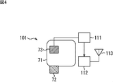
- FIG. 4 is a block diagram illustrating another configuration example of the imaging apparatus.
- the imaging apparatus 101 in FIG. 4 is different only in that the detector 74 is replaced with the trigger detector 111, the control object 75 is removed, and the wireless transmitter 113 with the antenna 114 is added.
- the configuration is basically the same as that of the imaging device 62 of FIG.
- the trigger detector 111 presets a current value change pattern as a trigger (hereinafter also referred to as an instruction trigger), and detects a trigger caused by a change in the current value of the OPD pixel 73.
- a shooting trigger and an image data transmission trigger, or a shooting and image data transmission trigger are set as triggers.
- a plurality of types of triggers may be set corresponding to the operation.
- the trigger 1 is set for shooting
- the trigger 2 is set for image data transmission.
- the trigger detector 111 outputs the detected trigger as a predetermined instruction to each corresponding unit, thereby causing the instruction to be performed.
- the trigger detector 111 causes the solid-state imaging device 71 to perform imaging when the trigger 1 is detected.
- the trigger detector 111 causes the wireless transmitter 112 to transmit image data captured by the solid-state imaging device 71.
- the wireless transmitter 112 When the wireless transmitter 112 receives an instruction from the trigger detector 111, the wireless transmitter 112 is activated and transmits image data from the solid-state imaging device 71 according to the instruction from the trigger detector 111 via the transmission antenna 114.
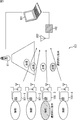
- FIG. 5 is a diagram illustrating a configuration example of an imaging system 151 to which the present technology is applied.
- the imaging system 151 is configured to include the light source 61, the imaging devices 101-1 to 101-4 in FIG. 4, and the PC 161.
- the imaging system 151 wireless communication is performed, but the imaging devices 101-1 to 101-4 all perform wireless communication in the same frequency band.
- each of the imaging devices 101-1 to 101-4 can be configured to detect (recognize) an individual trigger, and a large number of imaging devices 101-1 to 101-101 from a single light source 61. By selectively sending instructions to -4, wireless communication can be performed smoothly.
- the light source 61 can issue an instruction for one of many by combining temporal changes in intensity, changes in wavelength (color), and the like.
- a shooting trigger and a transmission trigger are set, and the light from the light source 61 is received and the trigger is detected from the change in the received current value.
- the imaging devices 101-1 to 101-4 detect a trigger, they perform processing corresponding to the trigger.
- the PC 161 has a wireless receiver 162 with an antenna 163.
- the PC 161 controls the light source 61 to set, for example, which imaging device 101 captures an image and which image device 101 transmits image data.
- Image data transmitted from the imaging devices 101-1 to 101-4 is received by the wireless receiver 162 via the antenna 163 and supplied to the PC 161.
- the imaging system 151 of FIG. 5 an example in which the light source 61 selectively instructs the imaging device 101-3 to capture images and the imaging device 101-4 selectively transmits image data. It is shown.
- step S111 the PC 161 controls the light source 61 to cause the light source 61 to emit light.
- Each OPD pixel 73 of the imaging devices 101-1 to 101-4 receives light and converts it into a current value in step S131.
- Each trigger detector 111 detects a trigger due to a change in each OPD pixel 73 in step S132.
- Each trigger detector 111 determines whether or not a trigger is detected in step S133. If it is determined in step S133 that a trigger has been detected, the process proceeds to step S134. For example, assume that the trigger detector 111 of the imaging apparatus 101-3 detects an imaging trigger, and the trigger detector 111 of the imaging apparatus 101-4 detects an image data transmission trigger.
- step S134 the trigger detector 111 determines whether or not the detected trigger is an imaging trigger. If it is determined in step S134 that the detected trigger is an imaging trigger, the process proceeds to step S135.
- step S135 the trigger detector 111 activates the solid-state imaging device 71 to capture an image.
- the solid-state imaging device 71 is activated and images. Image data obtained by imaging is temporarily stored in an image memory (not shown).
- step S134 If it is determined in step S134 that the detected trigger is not an imaging trigger, the process proceeds to step S136.
- the trigger detector 111 activates the wireless transmitter 112 to transmit image data.
- the wireless transmitter 112 is activated and transmits image data temporarily stored in an image memory (not shown).
- step S112 the wireless receiver 162 of the PC 161 receives the image data from the wireless transmitter 112 via the antenna 163.
- step S113 the PC 161 records the received image data in a storage unit (not shown).
- step S136 After step S136 or when it is determined in step S133 that no trigger has been detected, the process proceeds to step S137.
- step S137 the activated solid-state imaging device 71 and the wireless transmitter 112 (each unit other than the trigger detector 111) in the imaging device 101 stop operating and return to the state of ultra-low power consumption.
- the trigger detector 111 can detect the instruction trigger by temporally changing the light of the same color and frequency from the light source 61. Further, by setting a plurality of patterns that change with time of the light, the trigger detector 111 can detect a plurality of instruction triggers.
- the trigger detector 111 can detect different instruction triggers for each color by changing light of different colors and frequencies from the light source 61 with time.
- a trigger capable of separating light of different frequencies by emitting light of different frequencies (for example, visible light and infrared light (IR light)) from the light source 61 at the same time.
- different triggers can be detected at the same time.
- Example of instruction trigger> 8A to 8D are diagrams showing examples of instruction triggers.
- the trigger detector 111 can issue a system activation instruction to the main circuit 181 of the imaging device 62 by an instruction trigger as a result of detecting a change in the current value from the light of the light source 61. it can.
- the main circuit 181 is a part other than the trigger detector 111 in the imaging device 62.
- the trigger detector 111 detects the change in the current value from the light from the light source 61 and triggers the wireless transmitter 112 can be instructed to start transmission to a radio receiver 162 having an antenna 163.
- the trigger detector 111 is detected by an instruction trigger as a result of detecting a change in the current value from the light of the light source 61.
- Data consisting of a combination of changes in the current value can be sent to the data memory 182 of the wireless transmitter 112.
- the trigger detector 111 detects the change in the current value from the light from the light source 61 and triggers the solid-state imaging device. 71 can be made to perform photographing.
- the OPD pixel is an illuminance sensor built in the image sensor, an additional mechanism is unnecessary and cost performance is good.
- the power consumption is lower than in normal photographing.
- triggering with IR light it is possible to perform brightness measurement and trigger detection at the same time. Furthermore, when triggering is performed with IR light, it is possible to accept two types of triggers such as an instruction from a light source or a brightness change by an illuminometer.
- FIG. 9 is a diagram illustrating a usage example in which the above-described solid-state imaging device is used.
- the solid-state imaging device (image sensor) described above can be used in various cases for sensing light such as visible light, infrared light, ultraviolet light, and X-ray as follows.
- Devices for taking images for viewing such as digital cameras and mobile devices with camera functions
- Devices used for traffic such as in-vehicle sensors that capture the back, surroundings, and interiors of vehicles, surveillance cameras that monitor traveling vehicles and roads, and ranging sensors that measure distances between vehicles, etc.
- Equipment used for home appliances such as TVs, refrigerators, air conditioners, etc. to take pictures and operate the equipment according to the gestures ⁇ Endoscopes, equipment that performs blood vessel photography by receiving infrared light, etc.
- Equipment used for medical and health care ⁇ Security equipment such as security surveillance cameras and personal authentication cameras ⁇ Skin measuring instrument for photographing skin and scalp photography Such as a microscope to do beauty Equipment used for sports-Equipment used for sports such as action cameras and wearable cameras for sports applications-Used for agriculture such as cameras for monitoring the condition of fields and crops apparatus
- the present technology is not limited to application to a solid-state imaging device, but can also be applied to an imaging device.
- the imaging apparatus refers to a camera system such as a digital still camera or a digital video camera, or an electronic apparatus having an imaging function such as a mobile phone.
- a module-like form mounted on an electronic device that is, a camera module is used as an imaging device.
- the electronic apparatus 300 shown in FIG. 10 includes an imaging device (element chip) 301, an optical lens 302, a shutter device 303, a drive circuit 304, and a signal processing circuit 305.
- the solid-state imaging device 301 the solid-state imaging device 71 according to the first embodiment of the present technology described above is provided, and further includes a memory 72, an OPD pixel 73, a detector 74, and a control object 75 (not shown). . Thereby, the power consumption of the solid-state imaging device 301 of the electronic device 300 can be reduced.
- the optical lens 302 forms image light (incident light) from the subject on the imaging surface of the solid-state imaging device 301. As a result, signal charges are accumulated in the solid-state imaging device 301 for a certain period.
- the shutter device 303 controls the light irradiation period and the light shielding period for the solid-state imaging device 301.
- the drive circuit 304 supplies a drive signal for controlling the signal transfer operation of the solid-state imaging device 301 and the shutter operation of the shutter device 303.
- the solid-state imaging device 301 performs signal transfer by a drive signal (timing signal) supplied from the drive circuit 304.
- the signal processing circuit 305 performs various signal processing on the signal output from the solid-state imaging device 301.
- the video signal subjected to the signal processing is stored in a storage medium such as a memory or output to a monitor.
- the shutter device 303, the drive circuit 304, and the signal processing circuit 305 are in a stopped state, and are activated by an instruction from the detection circuit 74 as described above with reference to FIG.
- the configuration described as one device (or processing unit) may be divided and configured as a plurality of devices (or processing units).
- the configurations described above as a plurality of devices (or processing units) may be combined into a single device (or processing unit).
- a configuration other than that described above may be added to the configuration of each device (or each processing unit).
- a part of the configuration of a certain device (or processing unit) may be included in the configuration of another device (or other processing unit). . That is, the present technology is not limited to the above-described embodiment, and various modifications can be made without departing from the gist of the present technology.
- this technique can also take the following structures.
- a pixel that receives light from a light source and uses photoelectric conversion to convert the amount of received light into a current value;
- An imaging device comprising: a detection unit that detects a change in a current value of the pixel and performs an operation instruction according to a detection result.
- the pixel is a pixel specialized for detecting the brightness of the shooting environment, and is a pixel that converts a received light amount into a current value without using power by using photoelectric conversion.
- the detection unit detects at least one of light intensity, light reception time, blinking pattern, and wavelength as a change in the current value of the pixel. Imaging according to (1) or (2) apparatus.
- the detection unit detects an instruction trigger including a combination of changes in the current value of the pixel by temporally changing light of the same color and frequency from the light source.
- Imaging device By changing light of different colors and frequencies from the light source with time, the detection unit is configured by a combination of changes in the current value of the pixel, and detects different instruction triggers for each color. ).
- the detection unit By causing light of different frequencies from the light source to emit light at the same time, the detection unit includes a combination of changes in the current value of the pixel and detects instruction triggers of different frequencies at the same time.
- the imaging device according to 3).
- the imaging device is A control method that receives light from a light source, detects a change in the current value of a pixel that converts the amount of received light into a current value using photoelectric conversion, and issues an operation instruction according to the detection result.
- 1 solid-state imaging device 2 pixels, 3 pixel area, 11 semiconductor substrate, 51 imaging system, 61 light source, 62 imaging device, 71 solid-state imaging device, 72 memory, 73 OPD pixel, 74 detector, 75 control target, 101, 101 -1 to 101-4 Imaging device, 111 trigger detector, 112 wireless transmitter, 113 antenna, 151 imaging system, 161 PC, 162 wireless receiver, 163 antenna, 300 electronic device, 301 solid-state imaging device, 302 optical lens, 303 shutter device, 304 drive circuit, 305 signal processing circuit
Landscapes
- Engineering & Computer Science (AREA)
- Multimedia (AREA)
- Signal Processing (AREA)
- Transforming Light Signals Into Electric Signals (AREA)
- Studio Devices (AREA)
- Color Television Image Signal Generators (AREA)
Abstract
本開示は、低消費電力を実現することができるようにする撮像装置および制御方法に関する。 光源は、露光検出を行う画素であるOPD画素が受けられる波長の光源であり、その発光は、PCなどで制御される。OPD画素は、撮影環境の明るさを検出することに特化した画素であり、光電変換を利用して、電力消費なしに受光量を電流値に変換する。検出器は、OPD画素の電流値の変化(光の強度、受光時間、点滅パターンなど)を検出し、検出した場合、検出結果を、制御部に供給することで、図示せぬ他の装置、または、固体撮像装置に対して動作指示を行う。本開示は、例えば、OPD画素を備える固体撮像装置に適用することができる。
Description
本開示は、撮像装置および制御方法に関し、特に、低消費電力を実現することができるようにした撮像装置および制御方法に関する。
複数のカメラで撮影のために時刻を同期させる方法として、特許文献1においては、時刻同期情報算出方法が提案されており、この提案では、実際に撮像される画像に変換を与えることにより同期を行っている。
しかしながら、特許文献1に記載の提案では、同期のために撮影動作を行う必要があり、低消費電力を実現することが困難である。また、同期に使用した画像は、本来の撮影目的に使用することが難しく、無駄になってしまっていた。
本開示は、このような状況に鑑みてなされたものであり、低消費電力を実現することができるものである。
本技術の一側面の撮像装置は、光源からの光を受光し、光電変換を利用して、受光量を電流値に変換する画素と、前記画素の電流値の変化を検出し、検出結果に応じた動作指示を行う検出部とを備える。
前記画素は、撮影環境の明るさを検出することに特化した画素であり、光電変換を利用して、電力消費なしに受光量を電流値に変換する画素である。
前記検出部は、前記画素の電流値の変化として、光の強度、受光時間、点滅パターン、および波長の少なくともいずれか1つを検出することができる。
前記光源からの同一の色、周波数の光を時間的に変化させることで、前記検出部は、前記画素の電流値の変化の組み合わせからなる指示トリガを検出することができる。
前記光源からの異なる色、周波数の光を時間的に変化させることで、前記検出部は、前記画素の電流値の変化の組み合わせからなり、色別に異なる指示トリガを検出することができる。
前記光源からの異なる周波数の光を同一時間に発光させることで、前記検出部は、前記画素の電流値の変化の組み合わせからなり、同一時刻に異なる周波数の指示トリガを検出することができる。
前記検出部は、自分以外の各部に対するシステム起動指示を行うことができる。
前記検出部は、他の装置への画像データの送信指示を行うことができる。
前記検出部は、前記画素を含んで構成される固体撮像装置への撮像指示を行うことができる。
前記検出部は、前記画素の電流値の変化の組み合わせからなるデータの転送指示を行うことができる。
本発明の一側面の制御方法は、撮像装置が、光源からの光を受光し、光電変換を利用して、受光量を電流値に変換する画素の電流値の変化を検出し、検出結果に応じた動作指示を行う。
本技術の一側面においては、光源からの光が受光され、光電変換を利用して、受光量を電流値に変換する画素の電流値の変化が検出される。そして、その検出結果に応じた動作指示が行われる。
本技術によれば、低消費電力を実現することができる。
なお、本明細書に記載された効果は、あくまで例示であり、本技術の効果は、本明細書に記載された効果に限定されるものではなく、付加的な効果があってもよい。
以下、本開示を実施するための形態(以下実施の形態とする)について説明する。なお、説明は以下の順序で行う。
1.第1の実施の形態(撮像システムの例)
2.第2の実施の形態(変形例)
3.第3の実施の形態(イメージセンサの使用例)
4.第4の実施の形態(電子機器の例)
1.第1の実施の形態(撮像システムの例)
2.第2の実施の形態(変形例)
3.第3の実施の形態(イメージセンサの使用例)
4.第4の実施の形態(電子機器の例)
<第1の実施の形態(撮像システムの例)>
<固体撮像装置の概略構成例>
図1は、本技術の各実施の形態に適用されるCMOS(Complementary Metal Oxide Semiconductor)固体撮像装置の一例の概略構成例を示している。
<固体撮像装置の概略構成例>
図1は、本技術の各実施の形態に適用されるCMOS(Complementary Metal Oxide Semiconductor)固体撮像装置の一例の概略構成例を示している。
図1に示されるように、固体撮像装置(素子チップ)1は、半導体基板11(例えばシリコン基板)に複数の光電変換素子を含む画素2が規則的に2次元的に配列された画素領域(いわゆる撮像領域)3と、周辺回路部とを有して構成される。
画素2は、光電変換素子(例えばフォトダイオード)と、複数の画素トランジスタ(いわゆるMOSトランジスタ)を有してなる。複数の画素トランジスタは、例えば、転送トランジスタ、リセットトランジスタ、および増幅トランジスタの3つのトランジスタで構成することができ、さらに選択トランジスタを追加して4つのトランジスタで構成することもできる。各画素2(単位画素)の等価回路は一般的なものと同様であるので、ここでは詳細な説明は省略する。
また、画素2は、共有画素構造とすることもできる。画素共有構造は、複数のフォトダイオード、複数の転送トランジスタ、共有される1つのフローティングディフュージョン、および、共有される1つずつの他の画素トランジスタから構成される。
周辺回路部は、垂直駆動回路4、カラム信号処理回路5、水平駆動回路6、出力回路7、および制御回路8から構成される。
制御回路8は、入力クロックや、動作モード等を指令するデータを受け取り、また、固体撮像装置1の内部情報等のデータを出力する。具体的には、制御回路8は、垂直同期信号、水平同期信号、およびマスタクロックに基づいて、垂直駆動回路4、カラム信号処理回路5、および水平駆動回路6の動作の基準となるクロック信号や制御信号を生成する。そして、制御回路8は、これらの信号を垂直駆動回路4、カラム信号処理回路5、および水平駆動回路6に入力する。
垂直駆動回路4は、例えばシフトレジスタによって構成され、画素駆動配線を選択し、選択された画素駆動配線に画素2を駆動するためのパルスを供給し、行単位で画素2を駆動する。具体的には、垂直駆動回路4は、画素領域3の各画素2を行単位で順次垂直方向に選択走査し、垂直信号線9を通して各画素2の光電変換素子において受光量に応じて生成した信号電荷に基づいた画素信号をカラム信号処理回路5に供給する。
カラム信号処理回路5は、画素2の例えば列毎に配置されており、1行分の画素2から出力される信号を画素列毎にノイズ除去等の信号処理を行う。具体的には、カラム信号処理回路5は、画素2固有の固定パターンノイズを除去するためのCDS(Correlated Double Sampling)や、信号増幅、A/D(Analog/Digital)変換等の信号処理を行う。カラム信号処理回路5の出力段には、水平選択スイッチ(図示せず)が水平信号線10との間に接続されて設けられる。
水平駆動回路6は、例えばシフトレジスタによって構成され、水平走査パルスを順次出力することによって、カラム信号処理回路5の各々を順番に選択し、カラム信号処理回路5の各々から画素信号を水平信号線10に出力させる。
出力回路7は、カラム信号処理回路5の各々から水平信号線10を通して順次に供給される信号に対し、信号処理を行って出力する。出力回路7は、例えば、バッファリングだけを行う場合もあるし、黒レベル調整、列ばらつき補正、各種デジタル信号処理等を行う場合もある。
入出力端子12は、外部と信号のやりとりをするために設けられる。
<撮像システムの構成例>
図2は、本技術を適用した撮像システムの例を示すブロック図である。
図2は、本技術を適用した撮像システムの例を示すブロック図である。
図2に示される撮像システム51は、例えば、光源61および撮像装置62を含むように構成されている。なお、撮像システム51には、図示せぬ他の撮像装置62や他の装置も含まれている。
光源61は、露光検出を行う画素であるOPD(optical detector)画素73が受けられる波長の光源であり、その発光は、後述するPC(Personal Computer)などで制御される。
撮像装置62は、固体撮像装置71、メモリ72、OPD画素73、検出器74、および制御対象75を含むように構成されている。撮像装置62は、通常、検出器74を除いて、停止状態(超低消費電力状態)である。
固体撮像装置71は、画素2のうちの少なくとも1以上のいくつかをOPD画素73に入れ替えただけであり、その他は、固体撮像装置1と基本的に同様の構成とされる。OPD画素73の配置は、画素領域3内であれば、特に限定されない。
メモリ72は、生産時に記録される固定メモリであり、撮像装置62固有のIDを内蔵している。
OPD画素73は、撮影環境の明るさを検出することに特化した画素であり、光電変換を利用して、電力消費なしに受光量を電流値に変換する。OPD画素73は、撮影の条件(露光時間)を確認し調整するために予め備えられている。OPD画素73は、ダイナミックレンジを広くとることができる。なお、OPD画素73が埋め込まれていない場合、他の画素2を使うことも可能であるが、この場合、固体撮像装置71の起動が必要となる。
検出器74は、OPD画素73に電流があふれてくるので、OPD画素73の電流値の変化(光の強度、受光時間、点滅パターンなど)を検出し、検出した場合、検出結果に応じた動作指示を、制御対象75や固体撮像装置71に行う。
制御対象75は、検出器74からの検出結果に基づいて検出部74が動作指示を行う(制御する)対象である。その対象とは、例えば、撮像システム51に含まれる図示せぬ他の装置、または、撮像装置62の各部である。なお、他の装置に動作指示を行う場合、無線通信などの機能が具備される。
なお、固体撮像装置71内に、メモリ72、OPD画素73、検出器74、および制御対象75を含むように構成してもよい。
<撮像システムの処理例>
次に、図3のフローチャートを参照して、撮像システム51の処理について説明する。撮像装置62は、検出器74を除き、停止状態となっている。
次に、図3のフローチャートを参照して、撮像システム51の処理について説明する。撮像装置62は、検出器74を除き、停止状態となっている。
ステップS11において、光源61が発光する。ステップS12において、OPD画素73は、光源61からの光を受光し、受光量を電流値に変換する。
ステップS13において、検出器74は、OPD画素73に電流があふれてくるので、OPD画素73の電流値の変化(光の強度、受光時間、点滅パターンなど)を検出する。
ステップS14において、検出器74は、検出した場合、検出結果に応じた指示を、制御対象75である他の装置や撮像装置62の各部に行う。
例えば、固体撮像装置71への指示発行の場合、発行された指示を受けることで、固体撮像装置71は、停止状態から復帰し、受けとった指示に応じて動作開始する。また、例えば、制御対象75が指示を受け取った場合、制御対象75は、停止状態から復帰し、受けとった指示に応じて動作開始する。
<撮像装置の構成例>
図4は、撮像装置の他の構成例を示すブロック図である。
図4は、撮像装置の他の構成例を示すブロック図である。
図4の撮像装置101は、検出器74がトリガ検出器111に入れ替わった点と、制御対象75が除かれた点と、アンテナ114付きの無線送信器113が追加された点とが異なるだけであり、それ以外は、図2の撮像装置62と基本的に同様に構成されるため、その説明は省略される。
トリガ検出器111は、電流値の変化のパターンをトリガ(以下、指示トリガとも称する)として予め設定しており、OPD画素73の電流値の変化によるトリガを検出する。例えば、トリガ検出器111には、トリガとして、撮影のトリガと、画像データ送信のトリガ、あるいは、撮影および画像データ送信のトリガが設定されている。また、複数種類のトリガが動作に対応させて設定されていてもよい。例えば、トリガ1には撮影が対応されており、トリガ2には画像データ送信が対応されて設定されている。
トリガ検出器111は、検出したトリガを、所定の指示として、対応する各部に出力することで、その指示を行わせる。例えば、トリガ検出器111は、トリガ1が検出された場合、固体撮像装置71に撮影を行わせる。例えば、トリガ検出器111は、トリガ2が検出された場合、固体撮像装置71により撮影された画像データを、無線送信機112に送信させる。
無線送信機112は、トリガ検出器111からの指示を受けると、起動し、トリガ検出器111からの指示に応じた固体撮像装置71からの画像データを、送信アンテナ114を介して、送信する。
<撮像システムの構成例>
図5は、本技術を適用した撮像システム151の構成例を示す図である。
図5は、本技術を適用した撮像システム151の構成例を示す図である。
撮像システム151は、光源61、図4の撮像装置101-1乃至101-4、およびPC161を含むように構成されている。
撮像システム151においては、無線通信が行われるが、撮像装置101-1乃至101-4は、すべて同じ周波数帯で無線通信を行う。
そこで、撮像システム151においては、各撮像装置101-1乃至101-4を、それぞれが個別のトリガを検出(認識)できるように構成し、1つの光源61から多数の撮像装置101-1乃至101-4へ選択的に指示を送ることで、無線通信をスムーズに行うことができる。
光源61は、時間的な強度変化や波長(色)の変化などを組み合わせることで、多数の中から1つについて指示を出すことができる。
撮像装置101-1乃至101-4においては、それぞれ、撮影のトリガと送信のトリガが設定されており、光源61からの光を受け取り、受け取った電流値の変化からトリガを検出する。撮像装置101-1乃至101-4は、トリガを検出した場合、トリガに対応する処理を行う。
PC161は、アンテナ163付きの無線受信器162を有している。PC161は、光源61の制御を行い、例えば、どの撮像装置101により画像を撮影させ、どの撮像装置101からの画像データを送信するかなどを設定する。撮像装置101-1乃至101-4から送信されてくる画像データは、アンテナ163を介して、無線受信器162が受信し、PC161に供給される。
なお、図5の撮像システム151においては、光源61により、撮像装置101-3の撮影が選択的に指示されており、撮像装置101-4の画像データの送信が選択的に指示されている例が示されている。
<撮像システムの処理例>
図6のフローチャートを参照して、図5の撮像システムの処理について説明する。
図6のフローチャートを参照して、図5の撮像システムの処理について説明する。
PC161は、ステップS111において、光源61を制御し、光源61を発光させる。
撮像装置101-1乃至101-4の各OPD画素73は、それぞれ、ステップS131において、受光し、電流値に変換する。各トリガ検出器111は、ステップS132において、各OPD画素73の変化によるトリガを検出する。
各トリガ検出器111は、ステップS133において、トリガを検出したか否かを判定する。ステップS133において、トリガを検出したと判定された場合、処理は、ステップS134に進む。例えば、撮像装置101-3のトリガ検出器111において、撮像のトリガが検出されたとし、撮像装置101-4のトリガ検出器111において、画像データ送信のトリガが検出されたとする。
ステップS134において、トリガ検出器111は、検出されたトリガが、撮像のトリガであるか否かを判定する。ステップS134において、検出されたトリガが撮像のトリガであると判定された場合、処理は、ステップS135に進む。
ステップS135において、トリガ検出器111は、固体撮像装置71を起動させ、撮像させる。これに対応して、固体撮像装置71は起動して、撮像する。撮像による画像データは、図示せぬ画像メモリに一時保存される。
ステップS134において、検出されたトリガが撮像のトリガではないと判定された場合、処理は、ステップS136に進む。ステップS136において、トリガ検出器111は、無線送信器112を起動させ、画像データを送信させる。これに対応して、無線送信器112は、起動し、図示せぬ画像メモリに一時保存されている画像データを送信する。
ステップS112において、PC161の無線受信器162は、アンテナ163を介して、無線送信器112からの画像データを受信する。
ステップS113において、PC161は、図示せぬ記憶部に、受信された画像データを録する。
ステップS136の後、または、ステップS133においてトリガを検出していないと判定された場合、処理は、ステップS137に進む。
ステップS137において、撮像装置101のうち、起動した固体撮像装置71また無線送信器112(トリガ検出器111以外の各部)は、動作を停止し、超低消費電力の状態に戻る。
以上のようにすることで、動作をしている時以外は、超低消費電力の状態として、消費電力を低くすることができる。
<第2の実施の形態(変形例)>
<光源発光の例>
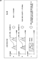
図7のA乃至図7のCは、光源発光の例を示す図である。
<光源発光の例>
図7のA乃至図7のCは、光源発光の例を示す図である。
図7のAに示されるように、光源61からの同一の色、周波数の光を時間的に変化させることで、トリガ検出器111においては、指示トリガを検出することができる。また、その光の時間的に変化させる複数のパターンを設定することで、トリガ検出器111においては、複数の指示トリガを検出することができる。
図7のBに示されるように、光源61からの異なる色、周波数の光を時間的に変化させることで、トリガ検出器111においては、色別に異なる指示トリガを検出することができる。
図7のCに示されるように、光源61からの異なる周波数の光(例えば、可視光と赤外光(IR光))を同一時間に発光させることで、異なる周波数の光を分離可能なトリガ検出器111においては、同一時刻に異なるトリガを検出することができる。
例えば、可視光での撮影と、赤外光でのトリガ検出を同時に行うことができる。また、OPD画素による露光調整用検波と赤外光からのトリガ検出を同時に行うことができる。
<指示トリガの例>
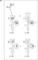
図8のA乃至図8のDは、指示トリガの例を示す図である。
図8のA乃至図8のDは、指示トリガの例を示す図である。
図8のAに示されるように、トリガ検出器111は、光源61の光からの電流値の変化を検出した結果の指示トリガにより、撮像装置62のメイン回路181に対するシステム起動指示を行うことができる。メイン回路181とは、撮像装置62における、トリガ検出器111以外の各部のことである。
図8のBに示されるように、トリガ検出器111は、無線送信器112がすでに起動している場合、光源61の光からの電流値の変化を検出した結果の指示トリガにより、無線送信器112に対して、アンテナ163を備える無線受信器162への送信開始指示を行うことができる。
図8のCに示されるように、トリガ検出器111は、無線送信器112がすでに起動している場合、光源61の光からの電流値の変化を検出した結果の指示トリガにより、その検出された電流値の変化の組み合わせでなるデータを、無線送信器112のデータメモリ182に送ることができる。
図8のDに示されるように、トリガ検出器111は、固体撮像装置71がすでに起動している場合、光源61の光からの電流値の変化を検出した結果の指示トリガにより、固体撮像装置71に撮影を行わせることができる。
以上のように、本技術によれば、OPD画素がイメージセンサに内蔵される照度センサであるので、追加の機構が不要であり、コストパフォーマンスがよい。また、センサ内蔵照度計と検出機構のみを動作させているので、通常の撮影に比べて低消費電力となる。
また、トリガをIR光で行う場合、撮影のための明るさ測定とトリガ検出を同時に行うことが可能である。さらに、トリガをIR光で行う場合、光源からの指示or照度計による明るさ変化など2種類のトリガを受け付けることが可能である。
<第3の実施の形態(イメージセンサの使用例)>
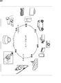
図9は、上述の固体撮像装置を使用する使用例を示す図である。
図9は、上述の固体撮像装置を使用する使用例を示す図である。
上述した固体撮像装置(イメージセンサ)は、例えば、以下のように、可視光や、赤外光、紫外光、X線等の光をセンシングする様々なケースに使用することができる。
・ディジタルカメラや、カメラ機能付きの携帯機器等の、鑑賞の用に供される画像を撮影する装置
・自動停止等の安全運転や、運転者の状態の認識等のために、自動車の前方や後方、周囲、車内等を撮影する車載用センサ、走行車両や道路を監視する監視カメラ、車両間等の測距を行う測距センサ等の、交通の用に供される装置
・ユーザのジェスチャを撮影して、そのジェスチャに従った機器操作を行うために、TVや、冷蔵庫、エアーコンディショナ等の家電に供される装置
・内視鏡や、赤外光の受光による血管撮影を行う装置等の、医療やヘルスケアの用に供される装置
・防犯用途の監視カメラや、人物認証用途のカメラ等の、セキュリティの用に供される装置
・肌を撮影する肌測定器や、頭皮を撮影するマイクロスコープ等の、美容の用に供される装置
・スポーツ用途等向けのアクションカメラやウェアラブルカメラ等の、スポーツの用に供される装置
・畑や作物の状態を監視するためのカメラ等の、農業の用に供される装置
・自動停止等の安全運転や、運転者の状態の認識等のために、自動車の前方や後方、周囲、車内等を撮影する車載用センサ、走行車両や道路を監視する監視カメラ、車両間等の測距を行う測距センサ等の、交通の用に供される装置
・ユーザのジェスチャを撮影して、そのジェスチャに従った機器操作を行うために、TVや、冷蔵庫、エアーコンディショナ等の家電に供される装置
・内視鏡や、赤外光の受光による血管撮影を行う装置等の、医療やヘルスケアの用に供される装置
・防犯用途の監視カメラや、人物認証用途のカメラ等の、セキュリティの用に供される装置
・肌を撮影する肌測定器や、頭皮を撮影するマイクロスコープ等の、美容の用に供される装置
・スポーツ用途等向けのアクションカメラやウェアラブルカメラ等の、スポーツの用に供される装置
・畑や作物の状態を監視するためのカメラ等の、農業の用に供される装置
<第4の実施の形態(電子機器の例)>
<電子機器の構成例>
<電子機器の構成例>
さらに、本技術は、固体撮像装置への適用に限られるものではなく、撮像装置にも適用可能である。ここで、撮像装置とは、デジタルスチルカメラやデジタルビデオカメラ等のカメラシステムや、携帯電話機等の撮像機能を有する電子機器のことをいう。なお、電子機器に搭載されるモジュール状の形態、すなわちカメラモジュールを撮像装置とする場合もある。
ここで、図10を参照して、本技術の第4の実施の形態の電子機器の構成例について説明する。
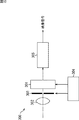
図10に示される電子機器300は、撮像装置(素子チップ)301、光学レンズ302、シャッタ装置303、駆動回路304、および信号処理回路305を備えている。固体撮像装置301としては、上述した本技術の第1の実施の形態の固体撮像装置71が設けられ、さらに、図示せぬメモリ72、OPD画素73、検出器74、および制御対象75が含まれる。これにより、電子機器300の固体撮像装置301の低電力化を行うことができる。
光学レンズ302は、被写体からの像光(入射光)を固体撮像装置301の撮像面上に結像させる。これにより、固体撮像装置301内に一定期間信号電荷が蓄積される。シャッタ装置303は、固体撮像装置301に対する光照射期間および遮光期間を制御する。
駆動回路304は、固体撮像装置301の信号転送動作およびシャッタ装置303のシャッタ動作を制御する駆動信号を供給する。駆動回路304から供給される駆動信号(タイミング信号)により、固体撮像装置301は信号転送を行う。信号処理回路305は、固体撮像装置301から出力された信号に対して各種の信号処理を行う。信号処理が行われた映像信号は、メモリなどの記憶媒体に記憶されたり、モニタに出力される。シャッタ装置303、駆動回路304、信号処理回路305は、停止状態であり、図3を参照して上述したように、検出回路74からの指示により起動する。
なお、本開示における実施の形態は、上述した実施の形態に限定されるものではなく、本開示の要旨を逸脱しない範囲において種々の変更が可能である。
また、以上において、1つの装置(または処理部)として説明した構成を分割し、複数の装置(または処理部)として構成するようにしてもよい。逆に、以上において複数の装置(または処理部)として説明した構成をまとめて1つの装置(または処理部)として構成されるようにしてもよい。また、各装置(または各処理部)の構成に上述した以外の構成を付加するようにしてももちろんよい。さらに、システム全体としての構成や動作が実質的に同じであれば、ある装置(または処理部)の構成の一部を他の装置(または他の処理部)の構成に含めるようにしてもよい。つまり、本技術は、上述した実施の形態に限定されるものではなく、本技術の要旨を逸脱しない範囲において種々の変更が可能である。
以上、添付図面を参照しながら本開示の好適な実施形態について詳細に説明したが、開示はかかる例に限定されない。本開示の属する技術の分野における通常の知識を有するのであれば、請求の範囲に記載された技術的思想の範疇内において、各種の変更例また修正例に想到し得ることは明らかであり、これらについても、当然に本開示の技術的範囲に属するものと了解される。
なお、本技術は以下のような構成も取ることができる。
(1) 光源からの光を受光し、光電変換を利用して、受光量を電流値に変換する画素と、
前記画素の電流値の変化を検出し、検出結果に応じた動作指示を行う検出部と
を備える撮像装置。
(2) 前記画素は、撮影環境の明るさを検出することに特化した画素であり、光電変換を利用して、電力消費なしに受光量を電流値に変換する画素である
前記(1)に記載の撮像装置。
(3) 前記検出部は、前記画素の電流値の変化として、光の強度、受光時間、点滅パターン、および波長の少なくともいずれか1つを検出する
前記(1)または(2)に記載の撮像装置。
(4) 前記光源からの同一の色、周波数の光を時間的に変化させることで、前記検出部は、前記画素の電流値の変化の組み合わせからなる指示トリガを検出する
前記(3)に記載の撮像装置。
(5) 前記光源からの異なる色、周波数の光を時間的に変化させることで、前記検出部は、前記画素の電流値の変化の組み合わせからなり、色別に異なる指示トリガを検出する
前記(3)に記載の撮像装置。
(6) 前記光源からの異なる周波数の光を同一時間に発光させることで、前記検出部は、前記画素の電流値の変化の組み合わせからなり、同一時刻に異なる周波数の指示トリガを検出する
前記(3)に記載の撮像装置。
(7) 前記検出部は、自分以外の各部に対するシステム起動指示を行う
前記(1)乃至(6)のいずれかに記載の撮像装置。
(8) 前記検出部は、他の装置への画像データの送信指示を行う
前記(1)乃至(6)のいずれかに記載の撮像装置。
(9) 前記検出部は、前記画素を含んで構成される固体撮像装置への撮像指示を行う
前記(1)乃至(6)のいずれかに記載の撮像装置。
(10) 前記検出部は、前記画素の電流値の変化の組み合わせからなるデータの転送指示を行う
前記(1)乃至(6)のいずれかに記載の撮像装置。
(11) 撮像装置が、
光源からの光を受光し、光電変換を利用して、受光量を電流値に変換する画素の電流値の変化を検出し、検出結果に応じた動作指示を行う
制御方法。
(1) 光源からの光を受光し、光電変換を利用して、受光量を電流値に変換する画素と、
前記画素の電流値の変化を検出し、検出結果に応じた動作指示を行う検出部と
を備える撮像装置。
(2) 前記画素は、撮影環境の明るさを検出することに特化した画素であり、光電変換を利用して、電力消費なしに受光量を電流値に変換する画素である
前記(1)に記載の撮像装置。
(3) 前記検出部は、前記画素の電流値の変化として、光の強度、受光時間、点滅パターン、および波長の少なくともいずれか1つを検出する
前記(1)または(2)に記載の撮像装置。
(4) 前記光源からの同一の色、周波数の光を時間的に変化させることで、前記検出部は、前記画素の電流値の変化の組み合わせからなる指示トリガを検出する
前記(3)に記載の撮像装置。
(5) 前記光源からの異なる色、周波数の光を時間的に変化させることで、前記検出部は、前記画素の電流値の変化の組み合わせからなり、色別に異なる指示トリガを検出する
前記(3)に記載の撮像装置。
(6) 前記光源からの異なる周波数の光を同一時間に発光させることで、前記検出部は、前記画素の電流値の変化の組み合わせからなり、同一時刻に異なる周波数の指示トリガを検出する
前記(3)に記載の撮像装置。
(7) 前記検出部は、自分以外の各部に対するシステム起動指示を行う
前記(1)乃至(6)のいずれかに記載の撮像装置。
(8) 前記検出部は、他の装置への画像データの送信指示を行う
前記(1)乃至(6)のいずれかに記載の撮像装置。
(9) 前記検出部は、前記画素を含んで構成される固体撮像装置への撮像指示を行う
前記(1)乃至(6)のいずれかに記載の撮像装置。
(10) 前記検出部は、前記画素の電流値の変化の組み合わせからなるデータの転送指示を行う
前記(1)乃至(6)のいずれかに記載の撮像装置。
(11) 撮像装置が、
光源からの光を受光し、光電変換を利用して、受光量を電流値に変換する画素の電流値の変化を検出し、検出結果に応じた動作指示を行う
制御方法。
1 固体撮像装置, 2 画素, 3 画素領域, 11 半導体基板, 51 撮像システム, 61 光源, 62 撮像装置, 71 固体撮像装置, 72 メモリ, 73 OPD画素, 74 検出器, 75 制御対象, 101,101-1乃至101-4 撮像装置, 111 トリガ検出器, 112 無線送信器, 113 アンテナ, 151 撮像システム, 161 PC, 162 無線受信器, 163 アンテナ, 300 電子機器, 301 固体撮像装置, 302 光学レンズ, 303 シャッタ装置, 304 駆動回路, 305 信号処理回路
Claims (11)
- 光源からの光を受光し、光電変換を利用して、受光量を電流値に変換する画素と、
前記画素の電流値の変化を検出し、検出結果に応じた動作指示を行う検出部と
を備える撮像装置。 - 前記画素は、撮影環境の明るさを検出することに特化した画素であり、光電変換を利用して、電力消費なしに受光量を電流値に変換する画素である
請求項1の記載の撮像装置。 - 前記検出部は、前記画素の電流値の変化として、光の強度、受光時間、点滅パターン、および波長の少なくともいずれか1つを検出する
請求項2の記載の撮像装置。 - 前記光源からの同一の色、周波数の光を時間的に変化させることで、前記検出部は、前記画素の電流値の変化の組み合わせからなる指示トリガを検出する
請求項3の記載の撮像装置。 - 前記光源からの異なる色、周波数の光を時間的に変化させることで、前記検出部は、前記画素の電流値の変化の組み合わせからなり、色別に異なる指示トリガを検出する
請求項3の記載の撮像装置。 - 前記光源からの異なる周波数の光を同一時間に発光させることで、前記検出部は、前記画素の電流値の変化の組み合わせからなり、同一時刻に異なる周波数の指示トリガを検出する
請求項3の記載の撮像装置。 - 前記検出部は、自分以外の各部に対するシステム起動指示を行う
請求項2の記載の撮像装置。 - 前記検出部は、他の装置への画像データの送信指示を行う
請求項2の記載の撮像装置。 - 前記検出部は、前記画素を含んで構成される固体撮像装置への撮像指示を行う
請求項2の記載の撮像装置。 - 前記検出部は、前記画素の電流値の変化の組み合わせからなるデータの転送指示を行う
請求項2の記載の撮像装置。 - 撮像装置が、
光源からの光を受光し、光電変換を利用して、受光量を電流値に変換する画素の電流値の変化を検出し、検出結果に応じた動作指示を行う
制御方法。
Priority Applications (2)
| Application Number | Priority Date | Filing Date | Title |
|---|---|---|---|
| CN201680034207.8A CN107710745B (zh) | 2015-06-19 | 2016-06-03 | 成像装置和控制方法 |
| US15/735,254 US10602071B2 (en) | 2015-06-19 | 2016-06-03 | Imaging device and control method |
Applications Claiming Priority (2)
| Application Number | Priority Date | Filing Date | Title |
|---|---|---|---|
| JP2015-124105 | 2015-06-19 | ||
| JP2015124105A JP2017011452A (ja) | 2015-06-19 | 2015-06-19 | 撮像装置および制御方法 |
Publications (1)
| Publication Number | Publication Date |
|---|---|
| WO2016203984A1 true WO2016203984A1 (ja) | 2016-12-22 |
Family
ID=57545665
Family Applications (1)
| Application Number | Title | Priority Date | Filing Date |
|---|---|---|---|
| PCT/JP2016/066543 Ceased WO2016203984A1 (ja) | 2015-06-19 | 2016-06-03 | 撮像装置および制御方法 |
Country Status (4)
| Country | Link |
|---|---|
| US (1) | US10602071B2 (ja) |
| JP (1) | JP2017011452A (ja) |
| CN (1) | CN107710745B (ja) |
| WO (1) | WO2016203984A1 (ja) |
Families Citing this family (1)
| Publication number | Priority date | Publication date | Assignee | Title |
|---|---|---|---|---|
| CN113821074B (zh) | 2021-09-06 | 2023-09-08 | 北京车和家信息技术有限公司 | 一种时间同步方法、装置、电子设备和存储介质 |
Citations (6)
| Publication number | Priority date | Publication date | Assignee | Title |
|---|---|---|---|---|
| JP2005191960A (ja) * | 2003-12-25 | 2005-07-14 | Casio Comput Co Ltd | 撮像装置、同期撮影支援装置、および、プログラム |
| JP2006186723A (ja) * | 2004-12-28 | 2006-07-13 | Casio Comput Co Ltd | 撮像装置、撮像方法、プログラム、及びプロジェクタシステム |
| WO2009091038A1 (ja) * | 2008-01-18 | 2009-07-23 | Nikon Corporation | 撮影用照明装置及びカメラ |
| WO2013179516A1 (ja) * | 2012-05-30 | 2013-12-05 | 富士フイルム株式会社 | 放射線画像撮影装置、放射線画像撮影システム、放射線画像撮影装置の制御プログラム、及び放射線画像撮影装置の制御方法 |
| JP2015023306A (ja) * | 2013-07-16 | 2015-02-02 | 株式会社東芝 | カメラ装置、室内撮像システム、室内情報取得装置 |
| WO2015064149A1 (ja) * | 2013-10-30 | 2015-05-07 | キヤノン株式会社 | 放射線撮影装置及び情報処理装置 |
Family Cites Families (13)
| Publication number | Priority date | Publication date | Assignee | Title |
|---|---|---|---|---|
| US9149175B2 (en) * | 2001-07-26 | 2015-10-06 | Given Imaging Ltd. | Apparatus and method for light control in an in-vivo imaging device |
| US9955551B2 (en) * | 2002-07-12 | 2018-04-24 | Yechezkal Evan Spero | Detector controlled illuminating system |
| KR100620966B1 (ko) * | 2004-12-15 | 2006-09-19 | 삼성전자주식회사 | 화면 적응적인 파워 제어 장치 및 그 방법 |
| JP5253000B2 (ja) * | 2008-06-03 | 2013-07-31 | オリンパス株式会社 | 撮像装置 |
| TWI445397B (zh) * | 2010-12-29 | 2014-07-11 | Altek Corp | 電子裝置、影像擷取裝置及其自動擷取影像之方法 |
| JPWO2013094115A1 (ja) | 2011-12-19 | 2015-04-27 | 日本電気株式会社 | 時刻同期情報算出装置、時刻同期情報算出方法および時刻同期情報算出プログラム |
| US10735216B2 (en) * | 2012-09-21 | 2020-08-04 | Google Llc | Handling security services visitor at a smart-home |
| US9208676B2 (en) * | 2013-03-14 | 2015-12-08 | Google Inc. | Devices, methods, and associated information processing for security in a smart-sensored home |
| JP5903634B2 (ja) * | 2012-11-16 | 2016-04-13 | パナソニックIpマネジメント株式会社 | 照明制御装置および照明システム |
| CN105723809B (zh) * | 2013-09-13 | 2018-11-20 | 库珀技术公司 | 用于基于智能传感器进行自动调试的系统、方法和装置 |
| JP6405243B2 (ja) * | 2014-03-26 | 2018-10-17 | キヤノン株式会社 | 焦点検出装置及びその制御方法 |
| CN204272238U (zh) * | 2014-12-12 | 2015-04-15 | 珠海艾派克微电子有限公司 | 一种成像装置 |
| CN104614856A (zh) * | 2015-02-16 | 2015-05-13 | 杭州清渠科技有限公司 | 一种基于复眼透镜光学结构的成像装置及其成像方法 |
-
2015
- 2015-06-19 JP JP2015124105A patent/JP2017011452A/ja active Pending
-
2016
- 2016-06-03 WO PCT/JP2016/066543 patent/WO2016203984A1/ja not_active Ceased
- 2016-06-03 US US15/735,254 patent/US10602071B2/en active Active
- 2016-06-03 CN CN201680034207.8A patent/CN107710745B/zh active Active
Patent Citations (6)
| Publication number | Priority date | Publication date | Assignee | Title |
|---|---|---|---|---|
| JP2005191960A (ja) * | 2003-12-25 | 2005-07-14 | Casio Comput Co Ltd | 撮像装置、同期撮影支援装置、および、プログラム |
| JP2006186723A (ja) * | 2004-12-28 | 2006-07-13 | Casio Comput Co Ltd | 撮像装置、撮像方法、プログラム、及びプロジェクタシステム |
| WO2009091038A1 (ja) * | 2008-01-18 | 2009-07-23 | Nikon Corporation | 撮影用照明装置及びカメラ |
| WO2013179516A1 (ja) * | 2012-05-30 | 2013-12-05 | 富士フイルム株式会社 | 放射線画像撮影装置、放射線画像撮影システム、放射線画像撮影装置の制御プログラム、及び放射線画像撮影装置の制御方法 |
| JP2015023306A (ja) * | 2013-07-16 | 2015-02-02 | 株式会社東芝 | カメラ装置、室内撮像システム、室内情報取得装置 |
| WO2015064149A1 (ja) * | 2013-10-30 | 2015-05-07 | キヤノン株式会社 | 放射線撮影装置及び情報処理装置 |
Also Published As
| Publication number | Publication date |
|---|---|
| US10602071B2 (en) | 2020-03-24 |
| JP2017011452A (ja) | 2017-01-12 |
| CN107710745B (zh) | 2021-03-16 |
| US20180183985A1 (en) | 2018-06-28 |
| CN107710745A (zh) | 2018-02-16 |
Similar Documents
| Publication | Publication Date | Title |
|---|---|---|
| US11856302B2 (en) | Systems and methods for digital imaging using computational pixel imagers with multiple in-pixel counters | |
| US9001220B2 (en) | Image sensor chip, method of obtaining image data based on a color sensor pixel and a motion sensor pixel in an image sensor chip, and system including the same | |
| US10291867B2 (en) | Solid-state imaging element and driving method and electronic equipment | |
| US10277848B2 (en) | Solid-state imaging device, method of driving the same, and electronic apparatus | |
| US7119842B2 (en) | Image capturing device including a spectrally-selectively transmissive diaphragm | |
| US20090147077A1 (en) | Light-source control system, shutter control system, endoscope processor, and endoscope system | |
| CN111343396A (zh) | 具有可控转换增益的图像传感器 | |
| WO2017126326A1 (ja) | 固体撮像装置およびその駆動方法、並びに電子機器 | |
| CN111193846B (zh) | 摄像设备 | |
| WO2016147885A1 (ja) | 固体撮像装置、固体撮像装置の駆動方法、及び、電子機器 | |
| WO2017183480A1 (ja) | 撮像装置および電子機器 | |
| US20180220092A1 (en) | Solid-state imaging device and electronic apparatus | |
| TWI751116B (zh) | 攝像元件、攝像方法及電子機器 | |
| US11463645B2 (en) | Solid-state imaging element and electronic device including a shared structure for pixels for sharing an AD converter | |
| JP2019140528A (ja) | 撮像装置、及び電子機器 | |
| JPWO2016121522A1 (ja) | 固体撮像装置および電子機器 | |
| US9648222B2 (en) | Image capturing apparatus that controls supply of amperage when reading out pixel signals and method for controlling the same | |
| US20070046809A1 (en) | Image pickup device, multi-eye image pickup device and control program for multi-eye image pickup device | |
| JP2021044623A (ja) | 撮像装置及びその制御方法 | |
| CN107710745B (zh) | 成像装置和控制方法 | |
| WO2024008305A1 (en) | An image sensor system, a camera module, an electronic device and a method for operating a camera module for detecting events using infrared | |
| WO2016147903A1 (ja) | 固体撮像装置および駆動方法、並びに電子機器 | |
| JP6954268B2 (ja) | 固体撮像装置、信号処理方法、および電子機器 | |
| US20200186739A1 (en) | Imaging device with switch circuit | |
| WO2016208416A1 (ja) | 固体撮像装置および電子機器 |
Legal Events
| Date | Code | Title | Description |
|---|---|---|---|
| 121 | Ep: the epo has been informed by wipo that ep was designated in this application |
Ref document number: 16811459 Country of ref document: EP Kind code of ref document: A1 |
|
| WWE | Wipo information: entry into national phase |
Ref document number: 15735254 Country of ref document: US |
|
| NENP | Non-entry into the national phase |
Ref country code: DE |
|
| 122 | Ep: pct application non-entry in european phase |
Ref document number: 16811459 Country of ref document: EP Kind code of ref document: A1 |