WO2016203971A1 - Data transfer device and data transfer method - Google Patents
Data transfer device and data transfer method Download PDFInfo
- Publication number
- WO2016203971A1 WO2016203971A1 PCT/JP2016/066394 JP2016066394W WO2016203971A1 WO 2016203971 A1 WO2016203971 A1 WO 2016203971A1 JP 2016066394 W JP2016066394 W JP 2016066394W WO 2016203971 A1 WO2016203971 A1 WO 2016203971A1
- Authority
- WO
- WIPO (PCT)
- Prior art keywords
- data
- unit
- transfer
- read
- buffer unit
- Prior art date
Links
Images


Classifications
-
- G—PHYSICS
- G06—COMPUTING; CALCULATING OR COUNTING
- G06F—ELECTRIC DIGITAL DATA PROCESSING
- G06F13/00—Interconnection of, or transfer of information or other signals between, memories, input/output devices or central processing units
- G06F13/14—Handling requests for interconnection or transfer
- G06F13/16—Handling requests for interconnection or transfer for access to memory bus
- G06F13/1668—Details of memory controller
- G06F13/1673—Details of memory controller using buffers
-
- G—PHYSICS
- G06—COMPUTING; CALCULATING OR COUNTING
- G06F—ELECTRIC DIGITAL DATA PROCESSING
- G06F13/00—Interconnection of, or transfer of information or other signals between, memories, input/output devices or central processing units
- G06F13/14—Handling requests for interconnection or transfer
- G06F13/36—Handling requests for interconnection or transfer for access to common bus or bus system
- G06F13/362—Handling requests for interconnection or transfer for access to common bus or bus system with centralised access control
-
- G—PHYSICS
- G06—COMPUTING; CALCULATING OR COUNTING
- G06F—ELECTRIC DIGITAL DATA PROCESSING
- G06F13/00—Interconnection of, or transfer of information or other signals between, memories, input/output devices or central processing units
- G06F13/38—Information transfer, e.g. on bus
-
- G—PHYSICS
- G06—COMPUTING; CALCULATING OR COUNTING
- G06F—ELECTRIC DIGITAL DATA PROCESSING
- G06F13/00—Interconnection of, or transfer of information or other signals between, memories, input/output devices or central processing units
- G06F13/38—Information transfer, e.g. on bus
- G06F13/40—Bus structure
- G06F13/4004—Coupling between buses
- G06F13/4027—Coupling between buses using bus bridges
- G06F13/4031—Coupling between buses using bus bridges with arbitration
Definitions
- the present invention relates to a data transfer device and a data transfer method.
- Priority is claimed on Japanese Patent Application No. 2015-120449, filed Jun. 15, 2015, the content of which is incorporated herein by reference.
- an imaging system such as a digital camera includes a plurality of LSIs (Large Scale Integration) to which various functional blocks are allocated.
- the plurality of LSIs are connected to a common bus for DMA (Direct Memory Access).
- DMA Direct Memory Access
- a plurality of functional blocks respectively assigned to a plurality of LSIs share one DRAM (Dynamic Random Access Memory) via a common bus.
- This type of imaging system comprises a bus arbiter.
- the bus arbiter controls access to the DRAM by each functional block by adjusting and receiving a DMA transfer request of each functional block accessing the DRAM. Specifically, the bus arbiter reduces bus utilization efficiency by, for example, reducing the bandwidth loss of the common bus that occurs when switching banks, and the bandwidth loss of the common bus that occurs when switching between reads and writes. Arbitration is performed to preferentially receive DMA transfer requests of functional blocks carrying high-priority processing while improving the performance to the maximum.
- the functional block needs to quickly output the stagnant DMA transfer request in order to suppress the delay of its own processing.
- the functional block that has output the DMA transfer request can not output the next DMA transfer request unless a predetermined time has elapsed after the DMA transfer request is accepted by the arbiter. . Therefore, even if congestion or the like of the common bus is eliminated and a margin is created in the bandwidth of the common bus, it becomes difficult to rapidly output the stagnant DMA transfer request.
- the present invention has been made in view of the above circumstances, and it is an object of the present invention to provide a data transfer apparatus and data transfer method capable of rapidly performing stagnant data transfer while effectively using the bandwidth of the common bus. I assume.
- the data transfer apparatus comprises: a buffer unit (12) for temporarily storing transfer data transferred to the common bus (180); and the buffer unit using input data as the transfer data.
- a write control unit (11) for writing and outputting a notification signal indicating that the input data has been written to the buffer unit; a read control unit (13) for reading the transfer data from the buffer unit;
- An interface unit (14) for transferring the transfer data read from the buffer unit to the common bus according to a predetermined bus protocol, and the read control unit transfers the data from the buffer unit based on the notification signal
- a band smoothing unit (15) for smoothing the band of the common bus by controlling the timing of reading data; Obtain.
- the band smoothing unit delays the notification signal output from the write control unit, whereby the read control unit operates as the buffer unit.
- a control signal for controlling the timing of reading the transfer data may be generated and output to the read control unit.
- the band smoothing unit sequentially writes pixel data constituting the input data to the buffer unit by the light control unit.
- the notification signals may be sequentially output as the control signal to the read control unit at predetermined time intervals by delaying the notification signals sequentially output from the write control unit.
- the band smoothing unit includes a FIFO memory (1501) for holding the notification signal sequentially output from the write control unit.
- a first counter (1502) for counting the number of notification signals not read among the notification signals held in the FIFO memory in response to the notification signals sequentially output from the write control unit;
- a second counter (1503) which counts up at a predetermined cycle until reaching a count value giving the predetermined time interval, and is initialized at the timing of reading the FIFO memory, and the count of the second counter
- the notification signal that the value has reached a predetermined value and the count value of the first counter is not read from the FIFO memory is the FIF If a value indicating the presence in memory, the read judgment unit to lead a notification signal that has not been read from said FIFO memory is output as the control signal (1504) may be provided.
- the data transfer method writes the input data to the buffer unit as the transfer data to be transferred to the common bus, and outputs a notification signal indicating that the input data has been written to the buffer unit.
- stagnant data transfer can be performed promptly while effectively using the bandwidth of the common bus.
- FIG. 8 is a diagram for describing an operation of the data transfer apparatus according to the first embodiment of the present invention, and a diagram for describing an example of image data to be transferred.
- FIG. 8 is a diagram for describing an operation of the data transfer apparatus according to the first embodiment of the present invention, and a diagram for describing an example of image data to be transferred.
- FIG. 8 is a diagram for describing an operation of the data transfer apparatus according to the first embodiment of the present invention, and a diagram for describing an example of image data to be transferred.
- FIG. 8 is a diagram for describing an operation of the data transfer apparatus according to the first embodiment of the present invention, and a diagram for describing an example of image data to be transferred.
- FIG. 7 is a diagram for explaining the operation of the data transfer apparatus according to the first embodiment of the present invention, and a timing chart for explaining the operation when the time until the DMA transfer request is accepted is short.
- FIG. 8 is a diagram for explaining the operation of the data transfer apparatus according to the first embodiment of the present invention, and a diagram for explaining the relationship between input data and output data when the time until the DMA transfer request is accepted is short. It is.
- FIG. 8 is a diagram for explaining the operation of the data transfer apparatus according to the first embodiment of the present invention, and a timing chart for explaining the operation when the time until the DMA transfer request is accepted is long.
- FIG. 8 is a diagram for explaining the operation of the data transfer device according to the first embodiment of the present invention, and for explaining the relationship between input data and output data when the time until the DMA transfer request is accepted is long. It is.
- FIG. 17 is a diagram for explaining the operation of a band smoothing unit included in the data transfer apparatus according to the third embodiment of the present invention, and a diagram for explaining the relationship between the remaining capacity of the buffer unit and the time interval between transfer data is there.
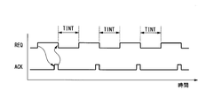
- FIG. 14 is a diagram for explaining an operation example of the data transfer device according to the related art for supplementing the effect of the data transfer device according to the embodiment of the present invention, and the operation when the time until the DMA transfer request is accepted is short It is a timing chart for explaining.
- FIG. 14 is a diagram for explaining an operation example of a data transfer device according to the related art for supplementing the effect of the data transfer device according to the embodiment of the present invention, and the operation when the time until the DMA transfer request is accepted is long It is a timing chart for explaining.
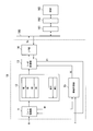
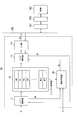
- FIG. 1 is a block diagram showing a configuration example of an imaging system 100 to which a data transfer apparatus according to a first embodiment of the present invention is applied.
- the imaging system 100 is, for example, a digital camera.
- the imaging system 100 includes an image sensor 110, functional blocks 120 to 150, a bus arbiter 161, a DRAM interface unit 162, a DRAM 163, a central processing unit (CPU) 170, and a common bus 180.
- CPU central processing unit
- FIG. 1 an optical system or the like for forming an optical image of a subject on an imaging surface of the image sensor 110 is omitted.
- the image sensor 110 photoelectrically converts a light image of a subject to generate pixel data (pixel signal).
- the image sensor 110 is, for example, a charge coupled device (CCD) image sensor or a complementary metal oxide semiconductor (CMOS) image sensor.
- CMOS complementary metal oxide semiconductor
- the image sensor 110 outputs, for example, image data of an RGB color system.
- the functional block 120 functions as a bus interface for outputting the image data obtained by the image sensor 110 to the common bus 180.
- the functional block 120 includes a preprocessing unit 121, image extraction units 122 and 123, an evaluation value generation unit 124, and data transfer units 125 to 127.
- the preprocessing unit 121 subjects the image data obtained by the image sensor 110 to preprocessing such as flaw correction and shading correction, for example.
- the image extracting units 122 and 123 extract image data such as a display image and a recording image from the image data by cutting out a part of the image data obtained by the image sensor 110.
- the evaluation value generation unit 124 generates an evaluation value used for control of exposure, white balance, focus and the like.
- the data transfer unit 125 transfers the image data extracted by the image extraction unit 122 to the common bus 180.
- the data transfer unit 126 transfers the image data extracted by the image extraction unit 123 to the common bus 180.
- the data transfer unit 127 transfers the evaluation value generated by the evaluation value generation unit 124 to the common bus 180.
- the function block 130 displays an image.
- the functional block 130 includes a data transfer unit 131, a display processing unit 132, and a display device 133.
- the data transfer unit 131 transfers image data of an image (hereinafter referred to as a display image) displayed on the display device 133 from the common bus 180 to the display processing unit 132.
- the display processing unit 132 acquires image data of a display image from the DRAM 163, and performs display processing such as OSD (On Screen Display) superposition processing on the image data.
- the display device 133 visualizes the image data processed by the display processing unit 132.
- the display device 133 is, for example, a TFT (Thin Film Transistor) liquid crystal device or an organic EL (ElectroLuminescence) display device.
- the function block 140 stores image data.
- the functional block 140 includes data transfer units 141 and 142, a card interface unit 143, and a recording medium 144.
- the data transfer unit 141 transfers the image data supplied from the card interface unit 143 to the common bus 180.
- the data transfer unit 142 transfers the image data supplied from the common bus 180 to the card interface unit 143.
- the card interface unit 143 reads image data from the DRAM 163 and writes the image data to the recording medium 144, and reads image data from the recording medium 144 and writes the image data to the DRAM 163.
- the recording medium 144 is, for example, a memory card removable from the card interface unit 143 such as an SD (Secure Digital) card or a CF (Compact Flash).
- the functional block 150 subjects the image data (preprocessed image data) stored in the DRAM 163 to predetermined image processing such as noise removal processing, YC conversion processing, resizing processing, JPEG compression processing, etc. Generate an image.
- the functional block 150 includes data transfer units 151 and 152, and an image processing unit 153.
- the data transfer unit 151 transfers the image data supplied from the image processing unit 153 to the common bus 180.
- the data transfer unit 152 transfers the image data supplied from the common bus 180 to the image processing unit 153.
- the image processing unit 153 performs the predetermined image processing.
- the image data subjected to the predetermined image processing by the image processing unit 153 is transferred to and stored in the DRAM 163.
- the bus arbiter 161 adjusts and receives DMA transfer requests output from the functional blocks 120 to 150 connected to the common bus 180.
- the bus arbiter 161 determines a functional block to which a bus right for permitting access to the DRAM 163 is given.
- the DRAM interface unit 162 performs writing of image data to the DRAM 163 and reading of image data from the DRAM 163.
- the DRAM 163 is a semiconductor memory shared by the functional blocks 120 to 150.
- the DRAM 163 is, for example, a synchronous DRAM.
- the central processing unit 170 controls the overall operation of the imaging system 100.
- the central processing unit 170 is also one of the functional blocks sharing the DRAM 163 in the same manner as the functional blocks 120 to 150 described above.
- the data transfer apparatus is a data transfer for outputting image data to the common bus 180 among the data transfer units 125 to 127, 131, 141, 142, 151, and 152 provided in the imaging system 100 described above. It corresponds to each of the units 125 to 127, 141, and 151.
- the following description focuses on the data transfer unit 125 included in the functional block 120, and the data transfer unit 125 is referred to as a “data transfer device 10”.
- the data transfer apparatus according to the first embodiment can be applied to all data transfer units provided in the imaging system 100 shown in FIG. 1 or can be applied to only some of the data transfer units.
- FIG. 2 is a block diagram showing a configuration example of the data transfer apparatus 10 according to the first embodiment of the present invention.
- the data transfer apparatus 10 includes a write control unit 11, a buffer unit 12, a read control unit 13, an interface unit (I / F unit) 14, and a band smoothing unit 15.
- the band smoothing unit 15 and the write control unit 11 may be integrated, or the band smoothing unit 15 and the read control unit 13 may be integrated. Further, the read control unit 13 and the interface unit 14 may be integrated.
- the light control unit 11 sequentially writes input image data Di, which is a data string of pixel data acquired by the image sensor 110, to the buffer unit 12 as transfer data.
- the write control unit 11 indicates that the input image data Di has been written to the buffer unit 12 each time writing of pixel data (for example, pixel data for 32 pixels) of a predetermined number of pixels constituting the input image data Di is completed.
- a write completion notification signal SW is output.
- the write completion notification signal SW includes address information indicating any of the storage areas M0 to M15 in which the input image data Di is written.
- the write control unit 11 outputs the write completion notification signal SW each time the writing of pixel data for 32 pixels constituting the input image data Di is completed, but the present invention is not limited to this example.
- the write control unit 11 receives a read completion notification signal SR from the read control unit 13 described later, the storage area in which transfer data is read out of the storage areas M0 to M15 based on the read completion notification signal SR. (Ie, a free storage area) is specified.
- the write control unit 11 writes the input image data Di in the free storage area.
- the buffer unit 12 temporarily stores transfer data transferred to the common bus 180.
- the buffer unit 12 is configured of, for example, a static random access memory (SRAM).
- the buffer unit 12 sequentially stores pixel data constituting the input image data Di in units of 64 bytes from the storage area M0 to the storage area M15. Specifically, the buffer unit 12 stores the first 32 pixels of 64 bytes of pixel data forming the input image data Di in the first storage area M0, and the next 32 pixels of 64 bytes of pixel data It stores in the storage area M1. In the same manner, the buffer unit 12 sequentially stores subsequent pixel data constituting the input image data Di in units of 64 bytes in the storage regions M2 to M15. When the input image data Di is stored in the last storage area M15, the buffer unit 12 again directs each new subsequent pixel data forming the input image data Di from the top storage area M0 to the storage area M15.
- each pixel data of the input image data Di sequentially output from the image sensor 110 is cyclically written by the write control unit 11 from the storage area M0 of the buffer unit 12 to the storage area M15.
- writing pixel data to the buffer unit 12 means writing the input image data Di to the storage areas M0 to M15 in units of 64 bytes for 32 pixels.
- the write clock signal for writing input image data Di to the buffer unit 12 and the read clock signal for reading transfer data from the buffer unit 12 are clock signals different from each other.
- the buffer unit 12 for example, an SRAM (for example, dual port SRAM) of a type capable of separately inputting a write clock signal and a read clock signal can be used.
- the read control unit 13 reads transfer data from the buffer unit 12 in response to a read control signal SC described later output from the band smoothing unit 15.
- the read control signal SC is a signal obtained by delaying the write completion notification signal SW. Therefore, the read control signal SC, like the write completion notification signal SW, together with the information indicating that the input image data Di has been written to the buffer unit 12, the address information indicating the storage area in which the input image data Di is written It contains.
- the read control signal SC is received from the band smoothing unit 15, the read control unit 13 receives 64-byte units for 32 pixels from the storage areas M0 to M15 of the buffer unit 12 indicated by the address information included in the read control signal SC. Read pixel data as transfer data.
- reading transfer data from the buffer unit 12 means reading pixel data from the storage areas M0 to M15 as transfer data in units of 64 bytes for 32 pixels.
- the read completion notification signal SR includes address information indicating the storage area of the buffer unit 12 in which the read transfer data has been stored (that is, information indicating an empty storage area).
- the interface unit 14 transfers transfer data read from the buffer unit 12 by the read control unit 13 to the common bus 180 according to a predetermined bus protocol. Specifically, in order to transfer transfer data to the common bus 180, the interface unit 14 transmits a DMA transfer request REQ, receives a DMA transfer acceptance ACK, and transmits an address ADD on the DRAM indicating a transfer destination of transfer data. , Transmission of transfer data (pixel data) body, etc.
- the band smoothing unit 15 smoothes the band of the common bus 180.
- the band smoothing unit 15 controls the bandwidth of the common bus 180 by controlling the timing at which the read control unit 13 reads transfer data from the buffer unit 12 based on the write completion notification signal SW input from the write control unit 11. Smooth out.
- the band smoothing unit 15 generates a read control signal SC for controlling the timing of reading transfer data from the buffer unit 12 by delaying the write completion notification signal SW input from the write control unit 11, and performs read control. Output to section 13.
- the read control signal SC generated by delaying the write completion notification signal SW is the write completion notification signal SW after smoothing.
- the band smoothing unit 15 sequentially outputs the light data output from the light control unit 11 as the pixel data constituting the input image data Di is sequentially written to the buffer unit 12 by the light control unit 11.
- the write completion notification signal is sequentially output to the read control unit 13 as the control signal at predetermined time intervals.
- the setting signal E for setting the predetermined time interval is input to the band smoothing unit 15 from the central processing unit 170 (FIG. 1).
- the setting signal E may be input to the band smoothing unit 15 directly from the outside. Details of the band smoothing unit 15 will be described later.
- FIG. 3 is a block diagram showing a configuration example of the band smoothing unit 15 provided in the data transfer apparatus 10 according to the first embodiment of the present invention.
- the band smoothing unit 15 includes a FIFO (First-In First-OUT) memory 1501, a counter (first counter) 1502, a counter (second counter) 1503, and a read determination unit 1504.
- FIFO First-In First-OUT
- first counter first counter
- second counter second counter
- the FIFO memory 1501 temporarily holds the write completion notification signal SW sequentially output from the write control unit 11.
- the FIFO memory 1501 is composed of, for example, a plurality of subordinately connected registers.
- the FIFO memory 1501 delays the write completion notification signal SW by temporarily holding the write completion notification signal SW, and performs read control of the write completion notification signal SW in accordance with a FIFO read instruction input from a read determination unit 1504 described later. It outputs as a signal SC.
- the counter (first counter) 1502 responds to the write completion notification signal SW sequentially output from the write control unit 11, and among the write completion notification signals SW already held in the FIFO memory 1501, the FIFO memory 1501. The number of write completion notification signals SW not read out is counted.
- the counter 1502 counts up each time the write completion notification signal SW is input from the write control unit 11 to the FIFO memory 1501.
- the counter 1502 counts down each time the write completion notification signal SW is read from the FIFO memory 1501.
- the count value of the counter 1502 represents a difference (a natural number including zero) between the number of write completion notification signals SW input to the FIFO memory 1501 and the number of write completion notification signals SW output from the FIFO memory 1501. Therefore, it can be known from the count value of the counter 1502 whether the write completion notification signal SW is not read from the FIFO memory 1501. If the count value of the counter 1502 is a value of 1 or more, a write completion notification signal SW not read from the FIFO memory 1501 exists in the FIFO memory 1501. If the count value of the counter 1502 is 0, all write completion notification signals SW input to the FIFO memory 1501 are read, and no write completion notification signals SW not read from the FIFO memory 1501 exist in the FIFO memory 1501. .
- the counter (second counter) 1503 counts up in a predetermined cycle until the count value reaches the maximum value of the count value set in the counter 1503 by the setting signal E.
- the counter 1503 outputs a signal indicating that the count value has reached the maximum value to the read determination unit 1504, and then the counter 1503 , And are initialized at the timing of reading of the FIFO memory 1501. That is, the count value of the counter 1503 is initialized each time the write completion notification signal SW is read from the FIFO memory 1501.
- the read determination unit 1504 outputs a FIFO read instruction
- the counter 1503 is initialized in response to the FIFO read instruction. After being initialized, the counter 1503 repeatedly counts up until the count value reaches the maximum value or is re-initialized.
- the time interval Ts of the read control signal SC sequentially output from the band smoothing unit 15 is determined.
- the time interval Ts (FIG. 6) of the read control signal SC is increased.
- the time interval of the read control signal SC becomes smaller.
- the smoothing of the common bus 180 tends to be suppressed.
- the maximum value of the count value set in the counter 1503 by the setting signal E can be arbitrarily set according to the required data transfer rate, the degree of smoothing of the band of the common bus 180, and the like.
- the read determination unit 1504 controls the reading of the FIFO memory 1501 based on the count values of the counters 1502 and 1503. That is, the read determination unit 1504 determines that the write completion notification signal SW in which the count value of the counter 1503 reaches a predetermined value determined based on the above maximum value and the count value of the counter 1502 is not read from the FIFO memory 1501 is FIFO. If the value indicates that the memory 1501 is present, a FIFO read instruction for instructing reading of the write completion notification signal SW is output to the FIFO memory 1501.
- the read determination unit 1504 outputs the FIFO read instruction to the FIFO memory 1501 to read and output the write completion notification signal SW not read from the FIFO memory 1501 from the FIFO memory 1501 as the read control signal SC.
- the read control signal SC is sequentially sent from the FIFO memory 1501 of the band smoothing unit 15 to the read control unit 13 with a predetermined time interval Ts (FIG. 6) determined by the maximum value of the count value set in the counter 1503. Output.
- Ts predetermined time interval
- the read control signal SC is input to the read control unit 13 at time intervals Ts, whereby the band of the common bus 180 is smoothed as described later.
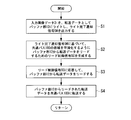
- FIG. 4 is a flow chart showing an example of the operation flow of the data transfer apparatus 10 according to the first embodiment of the present invention.
- 5A to 5D are diagrams for explaining the operation of the data transfer apparatus 10 according to the first embodiment of the present invention, and are diagrams for explaining examples of image data to be transferred.
- 6A and 6B are diagrams for explaining the operation of the data transfer apparatus 10 according to the first embodiment of the present invention.
- FIG. 6A is a timing chart for explaining the operation in the case where the time until the DMA transfer request is accepted is short.
- FIG. 6B is a diagram for explaining the relationship between input image data Di and output transfer data Do when the time until the DMA transfer request is accepted is short.
- 7A and 7B are diagrams for explaining the operation of the data transfer apparatus 10 according to the first embodiment of the present invention.
- FIG. 7A is a timing chart for explaining the operation in the case where the time until the DMA transfer request is accepted is long.
- FIG. 7B is a diagram for explaining the relationship between input image data Di and output transfer data Do when the time until the DMA transfer request is accepted is long.
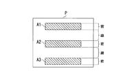
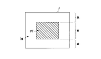
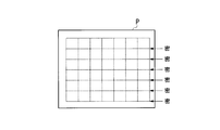
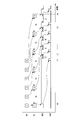
- FIG. 5A to 5D an example of the photographing screen P based on the input image data Di including an area in which pixel data to be transferred by the data transfer apparatus 10 is densely included and an area in which pixel data is sparsely included. It is shown.
- the imaging screen P shown in FIG. 5A includes an image area A1 to A3 in which an image (pixel data to be transferred) is captured and an image area (in which the image is hardly captured) (other than the image areas A1 to A3). Region).
- the input image data Di obtained from the image sensor 110 densely includes pixel data for displaying the image areas A1 to A3. In other words, pixel data is densely included in the image areas A1 to A3 (dense areas).
- the input image data Di contains almost no pixel data for displaying an area other than the image areas A1 to A3.
- the area other than the image areas A1 to A3 hardly includes pixel data (a sparse area).
- the input image data Di sequentially output from the image sensor 110 along the scanning line of the photographing screen P illustrated in FIG. 5A, the area (fine area) in which pixel data is densely included and the pixel data There are alternating areas (sparse areas) that hardly contain.
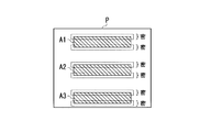
- the shooting screen P shown in FIG. 5B includes image areas A1 to A3 in which loading of an image (pixel data to be transferred) is performed, and an image in which loading of an image is hardly performed. And an area (an area other than the image areas A1 to A3).
- the pixel data to be actually transferred is only a part of pixel data on the upper side of each of the image areas A1 to A3 indicated by the dotted line and a part of pixel data on the lower side. .
- the pixel data of the area indicated by the dotted line is densely included in the input image data Di (dense area).
- Pixel data of the other areas are hardly included in the input image data Di (sparse area). Also in this case, the input image data Di sequentially output from the image sensor 110 along the scanning line of the photographing screen P almost includes an area (fine area) in which pixel data is densely included and pixel data. There are alternate areas (sparse areas) and no areas.
- the shooting screen P shown in FIG. 5C includes a wide-angle image PW and a telephoto image PT.
- pixel data of the shooting screen P including the wide-angle image PW and the telephoto image PT is transferred.
- the area of the telephoto image PT corresponds to an area in which an image (pixel data to be transferred) is captured. That is, the pixel data of the region of the telephoto image PT is densely included in the input image data Di (dense region).
- the other area (area of the wide-angle image PW) corresponds to an area where image capture is hardly performed.
- the pixel data of the other area is hardly included in the input image data Di (sparse area).
- the input image data Di sequentially output from the image sensor 110 along the scanning line of the photographing screen P almost includes an area (fine area) in which pixel data is densely included and pixel data. There are alternate areas (sparse areas) and no areas. The same applies to input image data acquired from the image sensor 110 by so-called digital zooming.
- the photographing screen P illustrated in FIG. 5D includes a plurality of evaluation areas for acquiring evaluation values such as exposure and white balance.
- the plurality of evaluation areas are indicated by dotted lines.
- the evaluation value is included in input image data Di corresponding to the last scanning line of each evaluation area. Therefore, the evaluation value is densely included in the input image data Di corresponding to the last scanning line of each evaluation area. That is, pixel data for evaluation is densely included in the area corresponding to the last scanning line of each evaluation area (dense area).
- the other areas contain pixel data for evaluation sparsely (sparse areas).
- the input image data Di includes a plurality of consecutive groups of six pieces of pixel data as one group.
- the present invention is not limited to this example, and the arrangement of pixel data included in the input image data Di is arbitrary.
- the write control unit of the data transfer apparatus 10 which is the data transfer unit 125 from the image extraction unit 122 in units of 64 bytes in which the pixel data constituting the input image data Di output from the image sensor 110 corresponds to pixel data for 32 pixels 11 are sequentially input.
- the write control unit 11 writes the input image data Di to the buffer unit 12 in units of 64 bytes for 32 pixels as transfer data to be transferred to the common bus 180 (step S1).
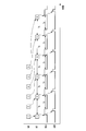
- step S1 each time the write control unit 11 writes 64-byte pixel data for 32 pixels included in the input image data Di to the buffer unit 12, the write control unit 11 writes the input image data Di to the buffer unit 12 as shown in FIG. 6A.
- a write completion notification signal SW indicating that it has been issued is output (step S1).
- the numbers in the rectangle schematically indicating the write completion notification signal SW correspond to six pixel data densely included in the input image data Di.
- the notation “1” is output from the light control unit 11 when the first (first) pixel data of the six pixel data densely included in the input image data Di is written to the buffer unit 12 Signal SW (1).
- the notation of such a signal is the same for the read control signal SC. That is, in FIG. 6A, the marks “1” to “6” of the write completion notification signal SW indicate the write completion notification signals SW (1) to SW (6).
- the marks “1” to “6” of the read control signal SC indicate read control signals SC (1) to SC (6).
- the band smoothing unit 15 generates the read control signal SC for reading transfer data from the buffer unit 12 so as to smooth the band of the common bus 180 based on the write completion notification signal SW (step S2). ).
- the band smoothing unit 15 sequentially inputs the write completion notification signal SW sequentially output from the write control unit 11 to the FIFO memory 1501 shown in FIG.
- the band smoothing unit 15 outputs the write completion notification signal SW held in the FIFO memory 1501 as the read control signal SC at a predetermined time interval Ts and in the input order.
- the write completion notification signals SW (1) to SW (6) output from the write control unit 11 to the band smoothing unit 15 and the read control signals SC (1) to SC output from the band smoothing unit 15 SC (6) is shown schematically.
- the time interval Ts of the read control signals SC (1) to SC (6) is determined based on the maximum value of the count value set in the counter 1503 shown in FIG. 3 described above.
- the transmission interval of the DMA transfer request REQ when transferring the input image data Di in which pixel data are densely present may be extended.
- the maximum value of the count value set in the counter 1503 shown in FIG. 3 is set such that the time interval Ts of the read control signal SC is larger than the time interval of the write completion notification signal SW.
- the time interval of the write completion notification signal SW corresponds to the time interval of the pixel data included in the input image data Di.
- the time interval Tr of the DMA transfer request REQ increases, so the data transfer rate tends to decrease.
- the time interval Ts of the read control signal SC is too large, it may occur that the process involving the subsequent data transfer is interrupted. For this reason, the maximum value of the count value set in the counter 1503 is set in a range where the required data transfer rate can be obtained.
- the read control unit 13 reads transfer data from the buffer unit 12 in response to the read control signal SC input from the band smoothing unit 15 (step S3).
- the read control unit 13 acknowledges the DMA transfer acceptance ACK for the DMA transfer request REQ of the previous transfer data. Is read by the interface unit 14, the transfer data of this time is read from the buffer unit 12.
- the interface unit 14 When the transfer data is read from the buffer unit 12 by the read control unit 13, the interface unit 14 outputs a DMA transfer request REQ to the common bus 180, and the transfer data read from the buffer unit 12 is shared according to a predetermined bus protocol. It transfers to the bus 180 (step S4). Specifically, as shown in FIG. 6A, six interface units 14 are provided corresponding to read control signals SC (1) to SC (6) input from band smoothing unit 15 at fixed time intervals Ts. The DMA transfer request REQ is sequentially output.
- the interface unit 14 performs the next DMA transfer request REQ. Before output, a DMA transfer acceptance ACK indicating that the present DMA transfer request REQ has been accepted by the bus arbiter 161 is received. Then, the interface unit 14 transfers the transfer data read from the buffer unit 12 by the read control unit 13 to the common bus 180 (step S4).
- the input image data Di closely including the six pixel data shown as the first group in FIG. 6B is set in the counter 1503.
- the output transfer data Do is output from the interface unit 14 to the common bus 180 at a time interval corresponding to the time interval Ts determined based on the maximum value of the count value.
- the data transfer of the pixel data of the first group is completed before the input image data Di including the pixel data of the second group following the first group closely.
- the bandwidth of the common bus 180 is smoothed to provide a time interval Tr for the DMA transfer request REQ. Therefore, when transferring input image data Di in which pixel data are densely present, the bus arbiter 161 can appropriately adjust and receive the DMA transfer request REQ of each functional block. This makes it possible to reduce the burden on the bus arbiter 161.
- the frequency of occupation of the common bus 180 by functional blocks transferring pixel data acquired from the image sensor 110 to the DRAM 163 is reduced by smoothing the band of the common bus 180.
- the frequency of DMA transfer requests REQ of other functional blocks being accepted by the bus arbiter 161 increases. Therefore, in the arbitration by the bus arbiter 161, even if the priority of the functional block for transferring the pixel data of the image sensor 110 to the DRAM 163 is set high, the influence on the processing of the other functional blocks can be suppressed. It is possible to prevent retention of processing of other functional blocks.
- the write control unit 11 notifies the write completion each time the input image data Di including the pixel data acquired from the image sensor 110 is written to the buffer unit 12.
- the signal SW is sequentially output (step S1).
- the band smoothing unit 15 sequentially outputs the read control signal SC at a predetermined time interval Ts (step S2).
- the read control unit 13 reads transfer data from the buffer unit 12 in response to the read control signal SC output from the band smoothing unit 15 (step S3).
- the interface unit 14 outputs the DMA transfer request REQ of the transfer data read by the read control unit 13 in response to the read control signal SC, and transfers the transfer data (step S4).
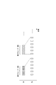
- the bus arbiter 161 it takes a long time until the first DMA transfer request REQ output from the interface unit 14 in response to the first read control signal SC (1) is received by the bus arbiter 161 due to, for example, congestion of the common bus 180.
- the bus arbiter 161 it takes a long time for the bus arbiter 161 to receive the first DMA transfer request REQ output from the interface unit 14 at time t0 at time t1.
- the DMA transfer acceptance ACK for the first DMA transfer request REQ is received by the interface unit 14 at time t1 after the third read control signal SC (3) is output.
- the read control unit 13 When the DMA transfer acceptance ACK is received by the interface unit 14 at time t1, the read control unit 13 responds to the second read control signal SC (2) in step S3 described above to transfer the next transfer from the buffer unit 12 Read the data Then, in step S4 described above, in response to the second read control signal SC (2), the interface unit 14 outputs the DMA transfer request REQ of the transfer data read by the read control unit 13 and the transfer data To the common bus 180.
- transfer data read from the buffer unit 12 by the read control unit 13 is temporarily retained in response to the second and subsequent read control signals SC (2) to SC (6).
- the transfer of the stagnant transfer data is promptly performed at short time intervals, and the transfer data is transferred. You can catch up with the transfer delay.
- the second read control signal SC (2) and the third read control signal SC (3) are output from the band smoothing unit 15. It has already been output to the read control unit 13. For this reason, when the DMA transfer acceptance ACK of the first transfer data read from the buffer unit 12 is received in response to the first read control signal SC (1), the read control unit 13 immediately performs the above-mentioned step S3. Then, in response to the second read control signal SC (2) from the buffer unit 12, the next transfer data is read. Then, in step S4 described above, the interface unit 14 outputs the DMA transfer request REQ of the transfer data read in response to the second read control signal SC (2) to the common bus 180, and also transfers the transfer data. Transfer to the common bus 180.
- DMA transfer request REQ can be received promptly after time t 1
- DMA transfer request REQ is not limited to the maximum value of the count value of counter 1503, and the minimum time interval is not limited. Output from the interface unit 14. For this reason, the second and subsequent transfer data that has stagnated can be transferred quickly, and delay in transfer of transfer data can be recovered.
- the delay of the data transfer of the pixel data of the first group is wound before the input image data Di closely containing the pixel data of the second group of the first group is input. . Therefore, it is possible to prevent the influence of processing due to the delay in transfer of the first transfer data of the first group. Therefore, according to the first embodiment, the stagnant data transfer can be performed promptly while effectively using the band of the common bus 180.
- FIG. 8 is a block diagram showing a configuration example of the band smoothing unit 25 provided in the data transfer apparatus according to the second embodiment of the present invention.
- the band smoothing unit 25 according to the second embodiment further includes a selector 1505 in the configuration of the band smoothing unit 15 according to the first embodiment shown in FIG. 3 described above. Others are the same as in the first embodiment.
- the selector 1505 receives, for example, two types of setting signals E1 and E2 from the central processing unit 170 shown in FIG. Further, the setting signal E3 is input from the image extraction unit 122.
- the setting signal E1 is a signal similar to the setting signal E in the first embodiment described above, and is a signal for setting the maximum value of the count value of the counter 1503.
- the setting signal E2 is a signal for setting the maximum value of the count value of the counter 1503 similarly to the setting signal E1.
- the maximum value of the count value set by the setting signal E2 is smaller than the maximum value of the count value set by the setting signal E1. Therefore, when the maximum value of the count value of the counter 1503 is set by the setting signal E2, the time of the DMA transfer request REQ is higher than when the maximum value of the count value of the counter 1503 is set by the setting signal E1. The interval Ts becomes short.
- the setting signal E3 is a signal including final transfer information indicating that the transfer data read from the buffer unit 12 by the read control unit 13 is the final transfer data.
- the selector 1505 selects the setting signal E2 and outputs the selected signal E2 to the counter 1503 and the read determination unit 1504. In other cases, the selector 1505 selects the setting signal E1 and outputs it to the counter 1503 and the read determination unit 1504.
- the image extracting unit 122 determines whether the input image data Di is the final transfer data in a frame. Determine if Then, when the input image data Di is not the final transfer data, the image extracting unit 122 outputs a setting signal E3 including final transfer information indicating that the input image data Di is not the final transfer data to the selector 1505 of the band smoothing unit 25. . In this case, the setting signal E1 is selected by the selector 1505 and output to the counter 1503 and the read determination unit 1504.
- the image extracting unit 122 determines that the input image data Di is the final transfer data.
- a setting signal E3 including final transfer information indicating that there is a signal is output to the selector 1505.
- the setting signal E2 is selected by the selector 1505 of the band smoothing unit 25 and output to the counter 1503 and the read determination unit 1504.
- the band smoothing unit 25 operates as in the first embodiment described above in normal data transfer other than final data transfer, and band smoothing of the common bus 180 is performed. Ru.
- the final data transfer a small value is set as the maximum value of the count value of the counter 1503 by the setting signal E2, so the time interval Ts of the read control signal SC becomes short, and the time interval Tr of the DMA transfer request REQ It becomes short.
- the band of the common bus can be smoothed while suppressing data interference between frames.
- FIG. 9 is a block diagram showing an example of the configuration of a data transfer apparatus 30 according to the third embodiment of the present invention.
- the data transfer apparatus 30 includes a band smoothing unit 35 in place of the band smoothing unit 15 in the configuration of the data transfer apparatus 10 shown in FIG. 2 according to the above-described first embodiment.
- the configuration of the other data transfer apparatus 30 is the same as that of the data transfer apparatus 10 of the first embodiment.
- FIG. 10 is a block diagram showing a configuration example of the band smoothing unit 35 provided in the data transfer apparatus 30 according to the third embodiment of the present invention.
- the band smoothing unit 35 further includes a buffer margin determination unit 1506 in the configuration of the band smoothing unit 25 shown in FIG. 8 according to the above-described second embodiment.
- the other configuration of the band smoothing unit 35 is the same as the configuration of the band smoothing unit 25 of the second embodiment.
- the buffer margin determination unit 1506 determines the remaining capacity (buffer margin) of the buffer unit 12.
- the band smoothing unit 35 adjusts the time interval between the transfer data transferred to the common bus 180 (time intervals Ts1 and Ts2 set by the setting signals E1 and E2) according to the determination result of the buffer margin determination unit 1506. Do. Specifically, the band smoothing unit 35 reduces the time interval Ts between transfer data as the remaining capacity of the buffer unit 12 decreases.
- the band smoothing unit 35 sets the time interval of the read control signal SC according to the setting signals E1 and E2 as in the second embodiment, and also performs the read control according to the remaining capacity of the buffer unit 12. Adjust the time interval of the signal SC. The adjustment of the time interval of the read control signal SC by the setting signals E1 and E2 may be omitted. In this case, the band smoothing of the common bus 180 is not performed.
- the band smoothing unit 35 determines the number of write completion notification signals SW (ie, the number of data written to the buffer unit 12) and the number of read control signals SC (ie, the number of data read from the buffer unit 12).
- the remaining capacity of the buffer unit 12 is obtained from the difference, and the remaining capacity of the buffer unit 12 is grasped from this remaining capacity.
- the small remaining capacity of the buffer unit 12 means that the possibility of being unable to write to the buffer unit 12 is increased, and the possibility that the function of the buffer unit 12 is impaired is increased.
- the buffer margin determination unit 1506 outputs a signal M indicating the remaining capacity (buffer margin) of the buffer unit 12 to the counter 1503.
- the signal M indicates that the remaining capacity of the buffer unit 12 has a margin, that the remaining capacity is small, or that there is almost no remaining capacity.
- the counter 1503 adjusts the maximum value of the count value set according to the setting signals E1 and E2 based on the signal M input from the buffer margin determination unit 1506.
- the band smoothing unit 35 sets a predetermined first coefficient "1" to a time interval Ts1 determined based on the setting signal E1.
- the time interval Ts11 obtained by multiplication is set as the time interval Ts of the read control signal SC.
- the time interval Ts of the transfer data Do transferred to the common bus 180 is set to a value equal to the time interval Ts1.
- band smoothing unit 35 multiplies time interval Ts1 determined based on setting signal E1 by a predetermined second coefficient "0.5".
- the time interval Ts12 is set as the time interval Ts of the read control signal SC.
- the band smoothing unit 35 sets a predetermined third coefficient “0.2” to the time interval Ts1 determined based on the setting signal E1.
- the multiplied time interval Ts13 is set as the time interval Ts of the read control signal SC.
- the respective numerical values of the first coefficient, the second coefficient, and the third coefficient are merely an example, and the numerical values of the respective coefficients may be arbitrarily selected as long as the remaining capacity of the buffer unit 12 can be adjusted. It can be set.
- the band smoothing unit 35 decreases the time interval Ts1 of the read control signal SC set by the setting signal E1 as the remaining capacity of the buffer unit 12 indicated by the signal M decreases, and the time between transfer data The interval Ts1 is decreased.
- the read speed from the buffer unit 12 is relatively increased more than the write speed to the buffer unit 12, and the remaining capacity of the buffer unit 12 is thereby increased.
- the data write operation to the buffer unit 12 can be stabilized. Function can be maintained stably.
- FIGS. 12A and 12B are diagrams for explaining an operation example of the data transfer device according to the related art for supplementing the effect of the data transfer device according to the embodiment of the present invention.
- FIG. 12A is a timing chart for explaining the operation in the case where the time until the DMA transfer request is accepted is short.
- FIG. 12B is a timing chart for explaining the operation in the case where the time until the DMA transfer request is accepted is long.
- the time interval TINT of the DMA transfer request REQ is fixed at a constant. Therefore, as illustrated in FIG. 12B, when it takes a long time from the output of the first DMA transfer request REQ to the common bus at time t10 to the reception of the DMA transfer acceptance ACK at time t11, the first After a predetermined time interval TINT from the DMA transfer request REQ, the next DMA transfer request REQ is output at time t12. In other words, even if the first DMA transfer request REQ is accepted, the next DMA transfer request REQ is not output unless a time corresponding to the fixed time interval TINT has elapsed. For this reason, it is not possible to quickly transfer the transfer data that has stagnated until the first DMA transfer request REQ is accepted.
- the time interval Tr of the DMA transfer request REQ is band smooth
- the DMA transfer request REQ is output at a minimum time interval without being limited to the time interval Ts of the read control signal SC output from the unit 15. Therefore, it is possible to promptly output the DMA transfer request REQ after the DMA transfer request REQ which took a long time to be accepted by the bus arbiter 161. Therefore, even if it takes a long time to receive the DMA transfer request REQ, the transfer data staying in that period can be transferred quickly, and a decrease in data transfer speed can be suppressed.
- the DMA transfer request REQ in the situation where the DMA transfer request REQ can be received promptly, in order to smooth the bandwidth of the common bus 180, the DMA transfer request REQ is The time interval Tr is set in accordance with the time interval Ts of the read control signal SC output from the band smoothing unit 15. Thus, even if the time interval Tr of the DMA transfer request REQ is set, the pixel data of each group does not interfere with each other as illustrated in FIG. 7A, so the data transfer rate is not impaired.
- the bandwidth of the common bus can be smoothed while suppressing data interference between frames.
- the buffer function of the buffer unit 12 can be stabilized. .
- the DMA transfer request REQ can be output according to the amount of transfer data held in the buffer unit 12, whereby the bandwidth of the common bus 180 can be flexibly smoothed according to the amount of transfer data. . Further, even if the DMA transfer request can not be received for a long time, it is possible to suppress retention of processing as a buffer of transfer data. In addition, the bandwidth can be controlled before outputting the DMA transfer request REQ, and the bandwidth control of the common bus 180 becomes easy. Further, since it is not necessary to provide a complicated circuit for controlling the time interval Tr of the DMA transfer request REQ, the scale of the circuit can be suppressed.
- the bandwidth of the common bus 180 can be smoothed. Therefore, while processing of a high priority functional block in arbitration by the bus arbiter 161 is performed, processing of a low priority functional block can be secured.
- the DMA transfer request REQ It takes a long time to be accepted, so it is possible to recover the delay of the stagnant data transfer.
- the band of the common bus 180 can be smoothed by spreading the DMA transfer request REQ on the time axis.
- the time interval Tr of the DMA transfer request REQ can be flexibly adjusted by the simple configuration. Further, even if the arbitration rule by the bus arbiter 161 is changed, the band of the common bus 180 can be flexibly smoothed by adjusting the maximum value of the count value of the counter 1503 by the setting signal E.
- the present invention can be widely applied to data transfer devices and data transfer methods, and can efficiently perform stagnant data transfer while effectively using the bandwidth of the common bus.
Landscapes
- Engineering & Computer Science (AREA)
- Theoretical Computer Science (AREA)
- General Engineering & Computer Science (AREA)
- Physics & Mathematics (AREA)
- General Physics & Mathematics (AREA)
- Computer Hardware Design (AREA)
- Bus Control (AREA)
- Information Transfer Systems (AREA)
- Image Processing (AREA)
Abstract
A data transfer device equipped with: a buffer unit for temporarily storing transfer data transferred from a common bus; a write control unit for writing input data to the buffer unit as the transfer data and outputting a notification signal indicating that the input data has been written to the buffer unit; a read control unit for reading the transfer data from the buffer unit; an interface unit for transferring the transfer data that was read from the buffer unit by the read control unit to the common bus in accordance with a prescribed bus protocol; and a band smoothing unit for smoothing the band of the common bus by controlling the timing at which the read control unit reads the transfer data from the buffer unit on the basis of the notification signal.
Description
本発明は、データ転送装置およびデータ転送方法に関する。
本願は、2015年6月15日に、日本に出願された特願2015-120449号に基づき優先権を主張し、その内容をここに援用する。 The present invention relates to a data transfer device and a data transfer method.
Priority is claimed on Japanese Patent Application No. 2015-120449, filed Jun. 15, 2015, the content of which is incorporated herein by reference.
本願は、2015年6月15日に、日本に出願された特願2015-120449号に基づき優先権を主張し、その内容をここに援用する。 The present invention relates to a data transfer device and a data transfer method.
Priority is claimed on Japanese Patent Application No. 2015-120449, filed Jun. 15, 2015, the content of which is incorporated herein by reference.
従来、デジタルカメラ等の撮像システムは、各種の機能ブロックが割り当てられた複数のLSI(Large Scale Integration)を備えている。複数のLSIは、DMA(Direct Memory Access)用の共通バスに接続されている。複数のLSIにそれぞれ割り当てられた複数の機能ブロックが共通バスを介して1つのDRAM(Dynamic Random Access Memory)を共有している。この種の撮像システムは、バスアービタを備える。
Conventionally, an imaging system such as a digital camera includes a plurality of LSIs (Large Scale Integration) to which various functional blocks are allocated. The plurality of LSIs are connected to a common bus for DMA (Direct Memory Access). A plurality of functional blocks respectively assigned to a plurality of LSIs share one DRAM (Dynamic Random Access Memory) via a common bus. This type of imaging system comprises a bus arbiter.
バスアービタは、DRAMにアクセスする各機能ブロックのDMA転送要求を調整して受け付けることにより、各機能ブロックによるDRAMへのアクセスを制御する。具体的には、バスアービタは、例えばバンクの切り替えの際に発生する共通バスの帯域ロスや、リードとライトの切り替えの際に発生する共通バスの帯域ロスを低減させることにより、バスの利用効率を最大限に向上させつつ、優先度の高い処理を担う機能ブロックのDMA転送要求を優先的に受け付けるようなアービトレーションを行う。
The bus arbiter controls access to the DRAM by each functional block by adjusting and receiving a DMA transfer request of each functional block accessing the DRAM. Specifically, the bus arbiter reduces bus utilization efficiency by, for example, reducing the bandwidth loss of the common bus that occurs when switching banks, and the bandwidth loss of the common bus that occurs when switching between reads and writes. Arbitration is performed to preferentially receive DMA transfer requests of functional blocks carrying high-priority processing while improving the performance to the maximum.
一般に、バスアービタによるアービトレーションによれば、優先度の高い機能ブロックがDMA転送要求を連続的に出力した場合、他の機能ブロックにバス権が渡らず、他の機能ブロックの処理が滞留する場合が起こり得る。この問題の解決を図った従来技術として、特許文献1に開示された技術がある。特許文献1の技術では、優先度の高い機能ブロックが一定の時間間隔を空けてDMA転送要求を出力することにより、たとえ優先度の高い機能ブロックのDMA転送要求が連続したとしても、バスアービタが優先度の低い他の機能ブロックのDMA転送要求を受け付けることを可能にしている。
Generally, according to the arbitration by the bus arbiter, when a high priority function block outputs a DMA transfer request continuously, the bus right may not be passed to other function blocks, and processing of other function blocks may occur. obtain. As a prior art aiming at the solution of this problem, there is a technique disclosed in Patent Document 1. In the technique of Patent Document 1, the bus arbiter gives priority even if DMA transfer requests of functional blocks with high priority are continued by outputting DMA transfer requests with high-priority functional blocks at fixed time intervals. It is possible to receive DMA transfer requests of other function blocks that are less frequent.
ところで、例えば共通バスの輻輳等により、機能ブロックのDMA転送要求がバスアービタに受け付けられるのに長時間を要した場合、その後に出力すべき当該機能ブロック自身のDMA転送要求が滞留する。この場合、当該機能ブロックは、自身の処理の遅滞を抑制するために、滞留したDMA転送要求を速やかに出力する必要がある。
By the way, for example, when it takes a long time for a DMA transfer request of a functional block to be accepted by the bus arbiter due to congestion of a common bus, etc., the DMA transfer request of the functional block itself to be output thereafter remains. In this case, the functional block needs to quickly output the stagnant DMA transfer request in order to suppress the delay of its own processing.
しかしながら、特許文献1の技術によれば、DMA転送要求がアービタに受け付けられてから一定時間経過後でなければ、当該DMA転送要求を出力した機能ブロックは次のDMA転送要求を出力することができない。このため、共通バスの輻輳等が解消し、共通バスの帯域に余裕が生まれても、滞留したDMA転送要求を速やかに出力することが困難になる。
However, according to the technique of Patent Document 1, the functional block that has output the DMA transfer request can not output the next DMA transfer request unless a predetermined time has elapsed after the DMA transfer request is accepted by the arbiter. . Therefore, even if congestion or the like of the common bus is eliminated and a margin is created in the bandwidth of the common bus, it becomes difficult to rapidly output the stagnant DMA transfer request.
本発明は、上記事情に鑑みてなされたものであり、共通バスの帯域を有効に利用しつつ、滞留したデータ転送を速やかに行うことができるデータ転送装置およびデータ転送方法を提供することを課題とする。
The present invention has been made in view of the above circumstances, and it is an object of the present invention to provide a data transfer apparatus and data transfer method capable of rapidly performing stagnant data transfer while effectively using the bandwidth of the common bus. I assume.
本発明の第1態様によれば、データ転送装置は、共通バス(180)に転送される転送データを一時的に格納するバッファ部(12)と、入力データを前記転送データとして前記バッファ部にライトし、前記入力データを前記バッファ部にライトした旨を示す通知信号を出力するライト制御部(11)と、前記バッファ部から前記転送データをリードするリード制御部(13)と、前記リード制御部により前記バッファ部からリードされた前記転送データを、所定のバスプロトコルに従って前記共通バスに転送するインターフェイス部(14)と、前記通知信号に基づいて、前記リード制御部が前記バッファ部から前記転送データをリードするタイミングを制御することにより、前記共通バスの帯域を平滑化する帯域平滑部(15)と、を備える。
According to the first aspect of the present invention, the data transfer apparatus comprises: a buffer unit (12) for temporarily storing transfer data transferred to the common bus (180); and the buffer unit using input data as the transfer data. A write control unit (11) for writing and outputting a notification signal indicating that the input data has been written to the buffer unit; a read control unit (13) for reading the transfer data from the buffer unit; An interface unit (14) for transferring the transfer data read from the buffer unit to the common bus according to a predetermined bus protocol, and the read control unit transfers the data from the buffer unit based on the notification signal A band smoothing unit (15) for smoothing the band of the common bus by controlling the timing of reading data; Obtain.
本発明の第2態様によれば、第1態様のデータ転送装置において、前記帯域平滑部は、前記ライト制御部から出力された前記通知信号を遅延させることにより、前記リード制御部が前記バッファ部から前記転送データをリードするタイミングを制御するための制御信号を生成して前記リード制御部に出力してもよい。
According to a second aspect of the present invention, in the data transfer apparatus according to the first aspect, the band smoothing unit delays the notification signal output from the write control unit, whereby the read control unit operates as the buffer unit. A control signal for controlling the timing of reading the transfer data may be generated and output to the read control unit.
本発明の第3態様によれば、第2態様のデータ転送装置において、前記帯域平滑部は、前記入力データを構成する画素データが前記ライト制御部により前記バッファ部に順次的にライトされるに従って前記ライト制御部から順次的に出力される前記通知信号を遅延させることにより、所定の時間間隔を空けて、前記通知信号を前記制御信号として前記リード制御部へ順次的に出力してもよい。
According to a third aspect of the present invention, in the data transfer apparatus according to the second aspect, the band smoothing unit sequentially writes pixel data constituting the input data to the buffer unit by the light control unit. The notification signals may be sequentially output as the control signal to the read control unit at predetermined time intervals by delaying the notification signals sequentially output from the write control unit.
本発明の第4態様によれば、第3態様のデータ転送装置において、前記帯域平滑部は、前記ライト制御部から順次的に出力される前記通知信号を保持するためのFIFOメモリ(1501)と、前記ライト制御部から順次的に出力される前記通知信号に応答して、前記FIFOメモリに保持された通知信号のうち、リードされていない通知信号の数をカウントする第1のカウンタ(1502)と、前記所定の時間間隔を与えるカウント値に到達するまで所定周期でカウントアップし、前記FIFOメモリのリードのタイミングで初期化される第2のカウンタ(1503)と、前記第2のカウンタのカウント値が所定値に到達し、且つ、前記第1のカウンタのカウント値が、前記FIFOメモリからリードされていない通知信号が前記FIFOメモリに存在することを示す値である場合、リードされていない通知信号を前記FIFOメモリからリードして前記制御信号として出力させるリード判定部(1504)と、を備えてもよい。
According to a fourth aspect of the present invention, in the data transfer device according to the third aspect, the band smoothing unit includes a FIFO memory (1501) for holding the notification signal sequentially output from the write control unit. A first counter (1502) for counting the number of notification signals not read among the notification signals held in the FIFO memory in response to the notification signals sequentially output from the write control unit; And a second counter (1503) which counts up at a predetermined cycle until reaching a count value giving the predetermined time interval, and is initialized at the timing of reading the FIFO memory, and the count of the second counter The notification signal that the value has reached a predetermined value and the count value of the first counter is not read from the FIFO memory is the FIF If a value indicating the presence in memory, the read judgment unit to lead a notification signal that has not been read from said FIFO memory is output as the control signal (1504) may be provided.
本発明の第5態様によれば、データ転送方法は、共通バスに転送される転送データとして入力データをバッファ部にライトし、前記入力データを前記バッファ部にライトした旨を示す通知信号を出力する第1ステップと、前記通知信号に基づいて、前記共通バスの帯域を平滑化するように前記バッファ部から前記転送データをリードするための制御信号を生成する第2ステップと、前記制御信号に応答して前記バッファ部から前記転送データをリードする第3ステップと、前記バッファ部からリードされた前記転送データを、所定のバスプロトコルに従って前記共通バスに転送する第4ステップと、を含む。
According to the fifth aspect of the present invention, the data transfer method writes the input data to the buffer unit as the transfer data to be transferred to the common bus, and outputs a notification signal indicating that the input data has been written to the buffer unit. A second step of generating a control signal for reading the transfer data from the buffer unit so as to smooth the band of the common bus based on the notification signal; And a fourth step of responsively reading the transfer data from the buffer unit, and transferring the transfer data read from the buffer unit to the common bus in accordance with a predetermined bus protocol.
本発明の各態様によれば、共通バスの帯域を有効に利用しつつ、滞留したデータ転送を速やかに行うことができる。
According to each aspect of the present invention, stagnant data transfer can be performed promptly while effectively using the bandwidth of the common bus.
以下、図面を参照しながら、本発明の実施形態を説明する。
(第1実施形態)
先ず、本発明の第1実施形態を説明する。
図1は、本発明の第1実施形態に係るデータ転送装置が適用された撮像システム100の構成例を示すブロック図である。
撮像システム100は、例えばデジタルカメラである。撮像システム100は、イメージセンサ110、機能ブロック120~150、バスアービタ161、DRAMインターフェイス部162、DRAM163、中央演算処理装置(CPU;Central Processing Unit)170、共通バス180を備えている。なお、図1では、イメージセンサ110の撮像面に被写体の光像を結像させるための光学系等は省略されている。 Hereinafter, embodiments of the present invention will be described with reference to the drawings.
First Embodiment
First, a first embodiment of the present invention will be described.
FIG. 1 is a block diagram showing a configuration example of animaging system 100 to which a data transfer apparatus according to a first embodiment of the present invention is applied.
Theimaging system 100 is, for example, a digital camera. The imaging system 100 includes an image sensor 110, functional blocks 120 to 150, a bus arbiter 161, a DRAM interface unit 162, a DRAM 163, a central processing unit (CPU) 170, and a common bus 180. In FIG. 1, an optical system or the like for forming an optical image of a subject on an imaging surface of the image sensor 110 is omitted.
(第1実施形態)
先ず、本発明の第1実施形態を説明する。
図1は、本発明の第1実施形態に係るデータ転送装置が適用された撮像システム100の構成例を示すブロック図である。
撮像システム100は、例えばデジタルカメラである。撮像システム100は、イメージセンサ110、機能ブロック120~150、バスアービタ161、DRAMインターフェイス部162、DRAM163、中央演算処理装置(CPU;Central Processing Unit)170、共通バス180を備えている。なお、図1では、イメージセンサ110の撮像面に被写体の光像を結像させるための光学系等は省略されている。 Hereinafter, embodiments of the present invention will be described with reference to the drawings.
First Embodiment
First, a first embodiment of the present invention will be described.
FIG. 1 is a block diagram showing a configuration example of an
The
イメージセンサ110は、被写体の光像を光電変換して画素データ(画素信号)を生成する。イメージセンサ110は、例えばCCD(Charge Coupled Device)イメージセンサまたはCMOS(Complementary Metal Oxide Semiconductor)イメージセンサである。イメージセンサ110は、例えばRGB表色系の画像データを出力する。
The image sensor 110 photoelectrically converts a light image of a subject to generate pixel data (pixel signal). The image sensor 110 is, for example, a charge coupled device (CCD) image sensor or a complementary metal oxide semiconductor (CMOS) image sensor. The image sensor 110 outputs, for example, image data of an RGB color system.
機能ブロック120は、イメージセンサ110により得られた画像データを共通バス180に出力するためのバスインターフェイスとして機能する。機能ブロック120は、前処理部121、画像抽出部122,123、評価値生成部124、データ転送部125~127を備えている。前処理部121は、イメージセンサ110により得られた画像データに対し、例えばキズ補正やシェーディング補正等の前処理を施す。
The functional block 120 functions as a bus interface for outputting the image data obtained by the image sensor 110 to the common bus 180. The functional block 120 includes a preprocessing unit 121, image extraction units 122 and 123, an evaluation value generation unit 124, and data transfer units 125 to 127. The preprocessing unit 121 subjects the image data obtained by the image sensor 110 to preprocessing such as flaw correction and shading correction, for example.
画像抽出部122,123は、イメージセンサ110により得られた画像データの一部を切り出すことにより、上記画像データから表示画像や記録画像等の画像データを抽出する。評価値生成部124は、露出、ホワイトバランス、フォーカス等の制御に用いられる評価値を生成する。データ転送部125は、画像抽出部122により抽出された画像データを共通バス180に転送する。データ転送部126は、画像抽出部123により抽出された画像データを共通バス180に転送する。データ転送部127は、評価値生成部124により生成された評価値を共通バス180に転送する。
The image extracting units 122 and 123 extract image data such as a display image and a recording image from the image data by cutting out a part of the image data obtained by the image sensor 110. The evaluation value generation unit 124 generates an evaluation value used for control of exposure, white balance, focus and the like. The data transfer unit 125 transfers the image data extracted by the image extraction unit 122 to the common bus 180. The data transfer unit 126 transfers the image data extracted by the image extraction unit 123 to the common bus 180. The data transfer unit 127 transfers the evaluation value generated by the evaluation value generation unit 124 to the common bus 180.
機能ブロック130は、画像を表示する。機能ブロック130は、データ転送部131、表示処理部132、表示デバイス133を備えている。データ転送部131は、表示デバイス133に表示される画像(以下、表示画像と称す。)の画像データを共通バス180から表示処理部132に転送する。表示処理部132は、DRAM163から表示画像の画像データを取得し、この画像データにOSD(On Screen Display)重畳処理等の表示処理を施す。表示デバイス133は、表示処理部132により処理された画像データを可視化する。表示デバイス133は、例えばTFT(Thin Film Transistor)液晶デバイスや有機EL(ElectroLuminescence)表示デバイスである。
The function block 130 displays an image. The functional block 130 includes a data transfer unit 131, a display processing unit 132, and a display device 133. The data transfer unit 131 transfers image data of an image (hereinafter referred to as a display image) displayed on the display device 133 from the common bus 180 to the display processing unit 132. The display processing unit 132 acquires image data of a display image from the DRAM 163, and performs display processing such as OSD (On Screen Display) superposition processing on the image data. The display device 133 visualizes the image data processed by the display processing unit 132. The display device 133 is, for example, a TFT (Thin Film Transistor) liquid crystal device or an organic EL (ElectroLuminescence) display device.
機能ブロック140は、画像データを記憶する。機能ブロック140は、データ転送部141,142、カードインターフェイス部143、記録媒体144を備えている。データ転送部141は、カードインターフェイス部143から供給される画像データを共通バス180に転送する。データ転送部142は、共通バス180から供給される画像データをカードインターフェイス部143に転送する。カードインターフェイス部143は、DRAM163から画像データをリードして記録媒体144にライトし、記録媒体144から画像データをリードしてDRAM163にライトする。記録媒体144は、例えばSD(Secure Digital)カードやCF(Compact Flash)等、カードインターフェイス部143に着脱可能なメモリカードである。
The function block 140 stores image data. The functional block 140 includes data transfer units 141 and 142, a card interface unit 143, and a recording medium 144. The data transfer unit 141 transfers the image data supplied from the card interface unit 143 to the common bus 180. The data transfer unit 142 transfers the image data supplied from the common bus 180 to the card interface unit 143. The card interface unit 143 reads image data from the DRAM 163 and writes the image data to the recording medium 144, and reads image data from the recording medium 144 and writes the image data to the DRAM 163. The recording medium 144 is, for example, a memory card removable from the card interface unit 143 such as an SD (Secure Digital) card or a CF (Compact Flash).
機能ブロック150は、DRAM163に格納された画像データ(前処理された画像データ)に対し、ノイズ除去処理、YC変換処理、リサイズ処理、JPEG圧縮処理等の所定の画像処理を施して表示画像や記録画像を生成する。機能ブロック150は、データ転送部151,152、画像処理部153を備えている。データ転送部151は、画像処理部153から供給された画像データを共通バス180に転送する。データ転送部152は、共通バス180から供給された画像データを画像処理部153に転送する。画像処理部153は、上記所定の画像処理を実施する。画像処理部153により上記所定の画像処理が施された画像データは、DRAM163に転送されて格納される。
The functional block 150 subjects the image data (preprocessed image data) stored in the DRAM 163 to predetermined image processing such as noise removal processing, YC conversion processing, resizing processing, JPEG compression processing, etc. Generate an image. The functional block 150 includes data transfer units 151 and 152, and an image processing unit 153. The data transfer unit 151 transfers the image data supplied from the image processing unit 153 to the common bus 180. The data transfer unit 152 transfers the image data supplied from the common bus 180 to the image processing unit 153. The image processing unit 153 performs the predetermined image processing. The image data subjected to the predetermined image processing by the image processing unit 153 is transferred to and stored in the DRAM 163.
バスアービタ161は、共通バス180に接続された機能ブロック120~150から出力されるDMA転送要求を調整して受け付ける。バスアービタ161は、DRAM163に対するアクセスを許可するためのバス権が付与される機能ブロックを決定する。DRAMインターフェイス部162は、DRAM163への画像データのライトとDRAM163からの画像データのリードとを実施する。DRAM163は、機能ブロック120~150により共有された半導体メモリである。DRAM163は、例えばシンクロナスDRAMである。
The bus arbiter 161 adjusts and receives DMA transfer requests output from the functional blocks 120 to 150 connected to the common bus 180. The bus arbiter 161 determines a functional block to which a bus right for permitting access to the DRAM 163 is given. The DRAM interface unit 162 performs writing of image data to the DRAM 163 and reading of image data from the DRAM 163. The DRAM 163 is a semiconductor memory shared by the functional blocks 120 to 150. The DRAM 163 is, for example, a synchronous DRAM.
中央演算処理装置170は、撮像システム100の全体動作を制御する。なお、中央演算処理装置170も、上述の機能ブロック120~150と同様に、DRAM163を共有する機能ブロックの一つである。
The central processing unit 170 controls the overall operation of the imaging system 100. The central processing unit 170 is also one of the functional blocks sharing the DRAM 163 in the same manner as the functional blocks 120 to 150 described above.
第1実施形態に係るデータ転送装置は、上述した撮像システム100に備えられたデータ転送部125~127,131,141,142,151,152のうち、共通バス180に画像データを出力するデータ転送部125~127,141,151のそれぞれに相当する。以下では、機能ブロック120に備えられたデータ転送部125に着目して説明することとし、データ転送部125を「データ転送装置10」と称す。
なお、第1実施形態に係るデータ転送装置は、図1に示す撮像システム100に備えられた全てのデータ転送部に適用することもでき、一部のデータ転送部にのみ適用することもできる。 The data transfer apparatus according to the first embodiment is a data transfer for outputting image data to thecommon bus 180 among the data transfer units 125 to 127, 131, 141, 142, 151, and 152 provided in the imaging system 100 described above. It corresponds to each of the units 125 to 127, 141, and 151. The following description focuses on the data transfer unit 125 included in the functional block 120, and the data transfer unit 125 is referred to as a “data transfer device 10”.
The data transfer apparatus according to the first embodiment can be applied to all data transfer units provided in theimaging system 100 shown in FIG. 1 or can be applied to only some of the data transfer units.
なお、第1実施形態に係るデータ転送装置は、図1に示す撮像システム100に備えられた全てのデータ転送部に適用することもでき、一部のデータ転送部にのみ適用することもできる。 The data transfer apparatus according to the first embodiment is a data transfer for outputting image data to the
The data transfer apparatus according to the first embodiment can be applied to all data transfer units provided in the
図2は、本発明の第1実施形態に係るデータ転送装置10の構成例を示すブロック図である。
データ転送装置10は、ライト制御部11、バッファ部12、リード制御部13、インターフェイス部(I/F部)14、帯域平滑部15を備えている。
なお、帯域平滑部15とライト制御部11とを一体化してもよく、帯域平滑部15とリード制御部13とを一体化してもよい。また、リード制御部13とインターフェイス部14とを一体化してもよい。 FIG. 2 is a block diagram showing a configuration example of thedata transfer apparatus 10 according to the first embodiment of the present invention.
The data transferapparatus 10 includes a write control unit 11, a buffer unit 12, a read control unit 13, an interface unit (I / F unit) 14, and a band smoothing unit 15.
Theband smoothing unit 15 and the write control unit 11 may be integrated, or the band smoothing unit 15 and the read control unit 13 may be integrated. Further, the read control unit 13 and the interface unit 14 may be integrated.
データ転送装置10は、ライト制御部11、バッファ部12、リード制御部13、インターフェイス部(I/F部)14、帯域平滑部15を備えている。
なお、帯域平滑部15とライト制御部11とを一体化してもよく、帯域平滑部15とリード制御部13とを一体化してもよい。また、リード制御部13とインターフェイス部14とを一体化してもよい。 FIG. 2 is a block diagram showing a configuration example of the
The data transfer
The
ライト制御部11は、イメージセンサ110によって取得された画素データのデータ列からなる入力画像データDiを転送データとしてバッファ部12に順次的にライトする。ライト制御部11は、入力画像データDiを構成する所定数の画素分の画素データ(例えば32画素分の画素データ)のライトが完了する都度、入力画像データDiをバッファ部12にライトした旨を示すライト完了通知信号SWを出力する。ライト完了通知信号SWには、入力画像データDiがライトされた記憶領域M0~M15の何れかを示すアドレス情報が含まれている。第1実施形態では、ライト制御部11は、入力画像データDiを構成する32画素分の画素データのライトが完了する都度、ライト完了通知信号SWを出力するが、この例に限定されない。
The light control unit 11 sequentially writes input image data Di, which is a data string of pixel data acquired by the image sensor 110, to the buffer unit 12 as transfer data. The write control unit 11 indicates that the input image data Di has been written to the buffer unit 12 each time writing of pixel data (for example, pixel data for 32 pixels) of a predetermined number of pixels constituting the input image data Di is completed. A write completion notification signal SW is output. The write completion notification signal SW includes address information indicating any of the storage areas M0 to M15 in which the input image data Di is written. In the first embodiment, the write control unit 11 outputs the write completion notification signal SW each time the writing of pixel data for 32 pixels constituting the input image data Di is completed, but the present invention is not limited to this example.
また、ライト制御部11は、後述するリード制御部13からリード完了通知信号SRを受信すると、そのリード完了通知信号SRに基づいて、記憶領域M0~M15のうち、転送データがリードされた記憶領域(即ち、空いた記憶領域)を特定する。ライト制御部11は、空いた記憶領域に入力画像データDiをライトする。
In addition, when the write control unit 11 receives a read completion notification signal SR from the read control unit 13 described later, the storage area in which transfer data is read out of the storage areas M0 to M15 based on the read completion notification signal SR. (Ie, a free storage area) is specified. The write control unit 11 writes the input image data Di in the free storage area.
バッファ部12は、共通バス180に転送される転送データを一時的に格納する。バッファ部12は、例えばSRAM(Static Random Access Memory)から構成される。第1実施形態では、バッファ部12は、記憶領域M0~M15の合計16個の記憶領域を含む。各記憶領域には、入力画像データDiを構成する上記所定数の画素分の画素データが転送データとして格納される。第1実施形態では、記憶領域M0~M15のそれぞれには、32画素分の画素データが格納される。1画素分の画素データを2バイトとすれば、記憶領域M0~M15のそれぞれには、64(=2×32)バイトの画素データが格納される。従って、記憶領域M0~M15のそれぞれは、少なくとも64バイトの記憶容量を有している。
The buffer unit 12 temporarily stores transfer data transferred to the common bus 180. The buffer unit 12 is configured of, for example, a static random access memory (SRAM). In the first embodiment, the buffer unit 12 includes a total of 16 storage areas of the storage areas M0 to M15. In each storage area, pixel data of the predetermined number of pixels constituting the input image data Di is stored as transfer data. In the first embodiment, pixel data of 32 pixels is stored in each of the storage areas M0 to M15. Assuming that pixel data for one pixel is 2 bytes, 64 (= 2 × 32) bytes of pixel data are stored in each of the storage areas M0 to M15. Therefore, each of the storage areas M0 to M15 has a storage capacity of at least 64 bytes.
バッファ部12は、記憶領域M0から記憶領域M15に向けて、入力画像データDiを構成する画素データを64バイト単位で順次的に格納する。具体的には、バッファ部12は、入力画像データDiを構成する最初の32画素分の64バイトの画素データを先頭の記憶領域M0に格納し、次の32画素分の64バイトの画素データを記憶領域M1に格納する。以下同様にして、バッファ部12は、入力画像データDiを構成する後続の画素データを64バイト単位で記憶領域M2~M15に順次格納する。最後の記憶領域M15に入力画像データDiが格納されると、バッファ部12は、再び先頭の記憶領域M0から記憶領域M15に向けて、入力画像データDiを構成する新たな後続の各画素データを64バイト単位で各記憶領域に順次的に格納する。即ち、バッファ部12の記憶領域M0から記憶領域M15には、イメージセンサ110から順次出力される入力画像データDiの各画素データがライト制御部11によって巡回的にライトされる。以下では、バッファ部12に画素データをライトすることは、記憶領域M0~M15に入力画像データDiを32画素分の64バイト単位でライトすることを意味する。
The buffer unit 12 sequentially stores pixel data constituting the input image data Di in units of 64 bytes from the storage area M0 to the storage area M15. Specifically, the buffer unit 12 stores the first 32 pixels of 64 bytes of pixel data forming the input image data Di in the first storage area M0, and the next 32 pixels of 64 bytes of pixel data It stores in the storage area M1. In the same manner, the buffer unit 12 sequentially stores subsequent pixel data constituting the input image data Di in units of 64 bytes in the storage regions M2 to M15. When the input image data Di is stored in the last storage area M15, the buffer unit 12 again directs each new subsequent pixel data forming the input image data Di from the top storage area M0 to the storage area M15. Store in each storage area sequentially in 64-byte units. That is, each pixel data of the input image data Di sequentially output from the image sensor 110 is cyclically written by the write control unit 11 from the storage area M0 of the buffer unit 12 to the storage area M15. In the following, writing pixel data to the buffer unit 12 means writing the input image data Di to the storage areas M0 to M15 in units of 64 bytes for 32 pixels.
なお、撮像システム100の構成上、バッファ部12に入力画像データDiをライトするためのライトクロック信号と、バッファ部12から転送データをリードするためのリードクロック信号とが、相互に異なるクロック信号である場合、バッファ部12として、例えば、ライトクロック信号とリードクロック信号とを個別に入力可能なタイプのSRAM(例えば、デュアルポートSRAM)を用いることができる。
Note that due to the configuration of the imaging system 100, the write clock signal for writing input image data Di to the buffer unit 12 and the read clock signal for reading transfer data from the buffer unit 12 are clock signals different from each other. In some cases, as the buffer unit 12, for example, an SRAM (for example, dual port SRAM) of a type capable of separately inputting a write clock signal and a read clock signal can be used.
リード制御部13は、帯域平滑部15から出力される後述のリード制御信号SCに応答して、バッファ部12から転送データをリードする。リード制御信号SCは、ライト完了通知信号SWを遅延させた信号である。従って、リード制御信号SCは、ライト完了通知信号SWと同様に、バッファ部12に入力画像データDiがライトされた旨を示す情報と共に、入力画像データDiがライトされた記憶領域を示すアドレス情報を含んでいる。リード制御部13は、帯域平滑部15からリード制御信号SCを受信すると、このリード制御信号SCに含まれるアドレス情報によって示されるバッファ部12の記憶領域M0~M15から32画素分の64バイト単位で画素データを転送データとしてリードする。以下では、バッファ部12から転送データをリードすることは、記憶領域M0~M15から画素データを転送データとして32画素分の64バイト単位でリードすることを意味する。
The read control unit 13 reads transfer data from the buffer unit 12 in response to a read control signal SC described later output from the band smoothing unit 15. The read control signal SC is a signal obtained by delaying the write completion notification signal SW. Therefore, the read control signal SC, like the write completion notification signal SW, together with the information indicating that the input image data Di has been written to the buffer unit 12, the address information indicating the storage area in which the input image data Di is written It contains. When the read control signal SC is received from the band smoothing unit 15, the read control unit 13 receives 64-byte units for 32 pixels from the storage areas M0 to M15 of the buffer unit 12 indicated by the address information included in the read control signal SC. Read pixel data as transfer data. In the following, reading transfer data from the buffer unit 12 means reading pixel data from the storage areas M0 to M15 as transfer data in units of 64 bytes for 32 pixels.
リード制御部13は、バッファ部12から32画素分の64バイトの転送データのリードを完了する都度、その転送データをリードした旨を示すリード完了通知信号SRをライト制御部11に出力する。リード完了通知信号SRには、リードされた転送データが格納されていたバッファ部12の記憶領域を示すアドレス情報(即ち、空いた記憶領域を示す情報)が含まれている。
Every time reading of transfer data of 64 bytes for 32 pixels is completed from the buffer unit 12, the read control unit 13 outputs a read completion notification signal SR indicating that the transfer data has been read to the write control unit 11. The read completion notification signal SR includes address information indicating the storage area of the buffer unit 12 in which the read transfer data has been stored (that is, information indicating an empty storage area).
インターフェイス部14は、リード制御部13によりバッファ部12からリードされた転送データを、所定のバスプロトコルに従って共通バス180に転送する。具体的には、インターフェイス部14は、転送データを共通バス180に転送するために、DMA転送要求REQの送信、DMA転送受付ACKの受信、転送データの転送先を示すDRAM上のアドレスADDの送信、転送データ(画素データ)本体の送信等を行う。
The interface unit 14 transfers transfer data read from the buffer unit 12 by the read control unit 13 to the common bus 180 according to a predetermined bus protocol. Specifically, in order to transfer transfer data to the common bus 180, the interface unit 14 transmits a DMA transfer request REQ, receives a DMA transfer acceptance ACK, and transmits an address ADD on the DRAM indicating a transfer destination of transfer data. , Transmission of transfer data (pixel data) body, etc.
帯域平滑部15は、共通バス180の帯域を平滑化する。帯域平滑部15は、ライト制御部11から入力されるライト完了通知信号SWに基づいて、リード制御部13がバッファ部12から転送データをリードするタイミングを制御することにより、共通バス180の帯域を平滑化する。帯域平滑部15は、ライト制御部11から入力されたライト完了通知信号SWを遅延させることにより、バッファ部12から転送データをリードするタイミングを制御するためのリード制御信号SCを生成してリード制御部13に出力する。ライト完了通知信号SWを遅延させることは、ライト完了通知信号SWを平滑化することを意味する。従って、ライト完了通知信号SWを遅延させることにより生成されるリード制御信号SCは、平滑化後のライト完了通知信号SWである。
The band smoothing unit 15 smoothes the band of the common bus 180. The band smoothing unit 15 controls the bandwidth of the common bus 180 by controlling the timing at which the read control unit 13 reads transfer data from the buffer unit 12 based on the write completion notification signal SW input from the write control unit 11. Smooth out. The band smoothing unit 15 generates a read control signal SC for controlling the timing of reading transfer data from the buffer unit 12 by delaying the write completion notification signal SW input from the write control unit 11, and performs read control. Output to section 13. To delay the write completion notification signal SW means to smooth the write completion notification signal SW. Therefore, the read control signal SC generated by delaying the write completion notification signal SW is the write completion notification signal SW after smoothing.
具体的には、帯域平滑部15は、入力画像データDiを構成する画素データがライト制御部11によりバッファ部12に順次的にライトされるに従ってライト制御部11から順次的に出力されるライト完了通知信号SWを遅延させることにより、所定の時間間隔を空けて、前記ライト完了通知信号を前記制御信号としてリード制御部13へ順次的に出力する。帯域平滑部15には、上記所定の時間間隔を設定するための設定信号Eが中央演算処理装置170(図1)から入力される。ただし、設定信号Eは、外部から直接的に帯域平滑部15に入力されてもよい。帯域平滑部15の詳細については後述する。
Specifically, the band smoothing unit 15 sequentially outputs the light data output from the light control unit 11 as the pixel data constituting the input image data Di is sequentially written to the buffer unit 12 by the light control unit 11. By delaying the notification signal SW, the write completion notification signal is sequentially output to the read control unit 13 as the control signal at predetermined time intervals. The setting signal E for setting the predetermined time interval is input to the band smoothing unit 15 from the central processing unit 170 (FIG. 1). However, the setting signal E may be input to the band smoothing unit 15 directly from the outside. Details of the band smoothing unit 15 will be described later.
図3は、本発明の第1実施形態に係るデータ転送装置10が備える帯域平滑部15の構成例を示すブロック図である。
帯域平滑部15は、FIFO(First-In First-OUT)メモリ1501、カウンタ(第1のカウンタ)1502,カウンタ(第2のカウンタ)1503、リード判定部1504を備えている。 FIG. 3 is a block diagram showing a configuration example of theband smoothing unit 15 provided in the data transfer apparatus 10 according to the first embodiment of the present invention.
Theband smoothing unit 15 includes a FIFO (First-In First-OUT) memory 1501, a counter (first counter) 1502, a counter (second counter) 1503, and a read determination unit 1504.
帯域平滑部15は、FIFO(First-In First-OUT)メモリ1501、カウンタ(第1のカウンタ)1502,カウンタ(第2のカウンタ)1503、リード判定部1504を備えている。 FIG. 3 is a block diagram showing a configuration example of the
The
FIFOメモリ1501は、ライト制御部11から順次的に出力されるライト完了通知信号SWを一時的に保持する。FIFOメモリ1501は、例えば、従属接続された複数のレジスタから構成される。FIFOメモリ1501は、ライト完了通知信号SWを一時的に保持することにより、ライト完了通知信号SWを遅延させ、後述するリード判定部1504から入力されるFIFOリード命令に従ってライト完了通知信号SWをリード制御信号SCとして出力する。
The FIFO memory 1501 temporarily holds the write completion notification signal SW sequentially output from the write control unit 11. The FIFO memory 1501 is composed of, for example, a plurality of subordinately connected registers. The FIFO memory 1501 delays the write completion notification signal SW by temporarily holding the write completion notification signal SW, and performs read control of the write completion notification signal SW in accordance with a FIFO read instruction input from a read determination unit 1504 described later. It outputs as a signal SC.
カウンタ(第1のカウンタ)1502は、ライト制御部11から順次的に出力されるライト完了通知信号SWに応答して、FIFOメモリ1501に既に保持されたライト完了通知信号SWのうち、FIFOメモリ1501からリードされていないライト完了通知信号SWの数をカウントする。カウンタ1502は、ライト制御部11からFIFOメモリ1501にライト完了通知信号SWが入力される都度、カウントアップする。また、カウンタ1502は、FIFOメモリ1501からライト完了通知信号SWがリードされる都度、カウントダウンする。
The counter (first counter) 1502 responds to the write completion notification signal SW sequentially output from the write control unit 11, and among the write completion notification signals SW already held in the FIFO memory 1501, the FIFO memory 1501. The number of write completion notification signals SW not read out is counted. The counter 1502 counts up each time the write completion notification signal SW is input from the write control unit 11 to the FIFO memory 1501. The counter 1502 counts down each time the write completion notification signal SW is read from the FIFO memory 1501.
カウンタ1502のカウント値は、FIFOメモリ1501に入力されたライト完了通知信号SWの数とFIFOメモリ1501から出力されたライト完了通知信号SWの数との差分(ゼロを含む自然数)を表す。従って、カウンタ1502のカウント値から、FIFOメモリ1501からリードされていないライト完了通知信号SWの有無を知ることができる。カウンタ1502のカウント値が1以上の値であれば、FIFOメモリ1501からリードされていないライト完了通知信号SWがFIFOメモリ1501に存在する。また、カウンタ1502のカウント値が0であれば、FIFOメモリ1501に入力されたライト完了通知信号SWは全てリードされ、FIFOメモリ1501からリードされていないライト完了通知信号SWはFIFOメモリ1501に存在しない。
The count value of the counter 1502 represents a difference (a natural number including zero) between the number of write completion notification signals SW input to the FIFO memory 1501 and the number of write completion notification signals SW output from the FIFO memory 1501. Therefore, it can be known from the count value of the counter 1502 whether the write completion notification signal SW is not read from the FIFO memory 1501. If the count value of the counter 1502 is a value of 1 or more, a write completion notification signal SW not read from the FIFO memory 1501 exists in the FIFO memory 1501. If the count value of the counter 1502 is 0, all write completion notification signals SW input to the FIFO memory 1501 are read, and no write completion notification signals SW not read from the FIFO memory 1501 exist in the FIFO memory 1501. .
カウンタ(第2のカウンタ)1503は、設定信号Eによってカウンタ1503に設定されるカウント値の最大値にカウント値が到達するまで所定周期でカウントアップする。カウンタ1503のカウント値が、設定信号Eによって設定される最大値に到達すると、カウンタ1503は、カウント値が最大値に到達した旨を示す信号をリード判定部1504に出力し、その後、カウンタ1503は、FIFOメモリ1501のリードのタイミングで初期化される。即ち、カウンタ1503のカウント値は、FIFOメモリ1501からライト完了通知信号SWがリードされる度に初期化される。具体的には、カウンタ1503は、リード判定部1504がFIFOリード命令を出力すると、そのFIFOリード命令に応答して初期化される。カウンタ1503は、初期化された後、カウント値が最大値に到達するか、または、再度、初期化されるまで、繰り返しカウントアップする。
The counter (second counter) 1503 counts up in a predetermined cycle until the count value reaches the maximum value of the count value set in the counter 1503 by the setting signal E. When the count value of the counter 1503 reaches the maximum value set by the setting signal E, the counter 1503 outputs a signal indicating that the count value has reached the maximum value to the read determination unit 1504, and then the counter 1503 , And are initialized at the timing of reading of the FIFO memory 1501. That is, the count value of the counter 1503 is initialized each time the write completion notification signal SW is read from the FIFO memory 1501. Specifically, when the read determination unit 1504 outputs a FIFO read instruction, the counter 1503 is initialized in response to the FIFO read instruction. After being initialized, the counter 1503 repeatedly counts up until the count value reaches the maximum value or is re-initialized.
設定信号Eによってカウンタ1503に設定されるカウント値の最大値に基づいて、帯域平滑部15から順次的に出力されるリード制御信号SCの時間間隔Tsが決まる。カウンタ1503に設定される上記最大値を増加させる程、リード制御信号SCの時間間隔Ts(図6)が大きくなる。この場合、共通バス180の帯域の平滑化が顕著になる一方、データの転送速度が低下する傾向を示す。逆に、上記最大値を減少させる程、リード制御信号SCの時間間隔が小さくなる。この場合、データの転送速度が上昇する一方、共通バス180の平滑化が抑制される傾向を示す。設定信号Eによってカウンタ1503に設定されるカウント値の最大値は、必要とされるデータ転送速度や共通バス180の帯域の平滑化の程度等に応じて任意に設定され得る。
Based on the maximum value of the count value set in the counter 1503 by the setting signal E, the time interval Ts of the read control signal SC sequentially output from the band smoothing unit 15 is determined. As the maximum value set in the counter 1503 is increased, the time interval Ts (FIG. 6) of the read control signal SC is increased. In this case, while the smoothing of the band of the common bus 180 becomes remarkable, the data transfer speed tends to decrease. Conversely, as the maximum value is decreased, the time interval of the read control signal SC becomes smaller. In this case, while the data transfer rate increases, the smoothing of the common bus 180 tends to be suppressed. The maximum value of the count value set in the counter 1503 by the setting signal E can be arbitrarily set according to the required data transfer rate, the degree of smoothing of the band of the common bus 180, and the like.
リード判定部1504は、カウンタ1502,1503のカウント値に基づいてFIFOメモリ1501のリードを制御する。即ち、リード判定部1504は、カウンタ1503のカウント値が上記最大値に基づいて決まる所定値に到達し、且つ、カウンタ1502のカウント値がFIFOメモリ1501からリードされていないライト完了通知信号SWがFIFOメモリ1501に存在することを示す値である場合、ライト完了通知信号SWのリードを指示するためのFIFOリード命令をFIFOメモリ1501に出力する。
The read determination unit 1504 controls the reading of the FIFO memory 1501 based on the count values of the counters 1502 and 1503. That is, the read determination unit 1504 determines that the write completion notification signal SW in which the count value of the counter 1503 reaches a predetermined value determined based on the above maximum value and the count value of the counter 1502 is not read from the FIFO memory 1501 is FIFO. If the value indicates that the memory 1501 is present, a FIFO read instruction for instructing reading of the write completion notification signal SW is output to the FIFO memory 1501.
リード判定部1504は、上記FIFOリード命令をFIFOメモリ1501に出力することにより、FIFOメモリ1501からリードされていないライト完了通知信号SWをFIFOメモリ1501からリード制御信号SCとしてリードして出力させる。このとき、リード制御信号SCは、カウンタ1503に設定されるカウント値の最大値によって定まる所定の時間間隔Ts(図6)を空けて、帯域平滑部15のFIFOメモリ1501からリード制御部13へ順次的に出力される。このように、リード制御信号SCが時間間隔Tsを空けてリード制御部13に入力されることにより、後述するように、共通バス180の帯域が平滑化される。
The read determination unit 1504 outputs the FIFO read instruction to the FIFO memory 1501 to read and output the write completion notification signal SW not read from the FIFO memory 1501 from the FIFO memory 1501 as the read control signal SC. At this time, the read control signal SC is sequentially sent from the FIFO memory 1501 of the band smoothing unit 15 to the read control unit 13 with a predetermined time interval Ts (FIG. 6) determined by the maximum value of the count value set in the counter 1503. Output. As described above, the read control signal SC is input to the read control unit 13 at time intervals Ts, whereby the band of the common bus 180 is smoothed as described later.
次に、図4に示すフローに沿って、図5Aから図7Bを参照しながら、第1実施形態に係るデータ転送装置10の動作(データ転送方法)を説明する。
図4は、本発明の第1実施形態に係るデータ転送装置10の動作フローの一例を示すフローチャートである。図5A~図5Dは、本発明の第1実施形態に係るデータ転送装置10の動作を説明するための図であり、転送対象の画像データの例を説明するための図である。図6Aおよび図6Bは、本発明の第1実施形態に係るデータ転送装置10の動作を説明するための図である。図6Aは、DMA転送要求が受け付けられるまでの時間が短い場合の動作を説明するためのタイミングチャートである。図6Bは、DMA転送要求が受け付けられるまでの時間が短い場合の入力画像データDiと出力転送データDoとの関係を説明するための図である。図7Aおよび図7Bは、本発明の第1実施形態に係るデータ転送装置10の動作を説明するための図である。図7Aは、DMA転送要求が受け付けられるまでの時間が長い場合の動作を説明するためのタイミングチャートである。図7Bは、DMA転送要求が受け付けられるまでの時間が長い場合の入力画像データDiと出力転送データDoとの関係を説明するための図である。 Next, the operation (data transfer method) of thedata transfer apparatus 10 according to the first embodiment will be described according to the flow shown in FIG. 4 and with reference to FIGS. 5A to 7B.
FIG. 4 is a flow chart showing an example of the operation flow of thedata transfer apparatus 10 according to the first embodiment of the present invention. 5A to 5D are diagrams for explaining the operation of the data transfer apparatus 10 according to the first embodiment of the present invention, and are diagrams for explaining examples of image data to be transferred. 6A and 6B are diagrams for explaining the operation of the data transfer apparatus 10 according to the first embodiment of the present invention. FIG. 6A is a timing chart for explaining the operation in the case where the time until the DMA transfer request is accepted is short. FIG. 6B is a diagram for explaining the relationship between input image data Di and output transfer data Do when the time until the DMA transfer request is accepted is short. 7A and 7B are diagrams for explaining the operation of the data transfer apparatus 10 according to the first embodiment of the present invention. FIG. 7A is a timing chart for explaining the operation in the case where the time until the DMA transfer request is accepted is long. FIG. 7B is a diagram for explaining the relationship between input image data Di and output transfer data Do when the time until the DMA transfer request is accepted is long.
図4は、本発明の第1実施形態に係るデータ転送装置10の動作フローの一例を示すフローチャートである。図5A~図5Dは、本発明の第1実施形態に係るデータ転送装置10の動作を説明するための図であり、転送対象の画像データの例を説明するための図である。図6Aおよび図6Bは、本発明の第1実施形態に係るデータ転送装置10の動作を説明するための図である。図6Aは、DMA転送要求が受け付けられるまでの時間が短い場合の動作を説明するためのタイミングチャートである。図6Bは、DMA転送要求が受け付けられるまでの時間が短い場合の入力画像データDiと出力転送データDoとの関係を説明するための図である。図7Aおよび図7Bは、本発明の第1実施形態に係るデータ転送装置10の動作を説明するための図である。図7Aは、DMA転送要求が受け付けられるまでの時間が長い場合の動作を説明するためのタイミングチャートである。図7Bは、DMA転送要求が受け付けられるまでの時間が長い場合の入力画像データDiと出力転送データDoとの関係を説明するための図である。 Next, the operation (data transfer method) of the
FIG. 4 is a flow chart showing an example of the operation flow of the
ここでは、第1実施形態による効果に関する理解を容易化するため、入力画像データDiには、画素データが密に含まれる領域と、画素データが疎に含まれる領域が存在するものとする。一般に、画素データが密に含まれる入力画像データDiを或る機能ブロックから共通バス180に転送する場合、当該機能ブロックはDMA転送要求を連続的に出力する。このため、DMA転送要求が出力される期間、他の機能ブロックのDMA転送要求がバスアービタに受け付けられなくなる状況が発生し得る。このような状況を回避するため、第1実施形態では、共通バス180の帯域を平滑化する。しかし、共通バス180の帯域を平滑化すると、DMA転送要求が制限され、データ転送速度が低下する場合が起こり得る。そこで、本実施形態では、共通バス180の帯域を平滑化しつつ、データ転送速度の低下を抑制することを可能とする効果を得る。
Here, in order to facilitate understanding of the effect according to the first embodiment, it is assumed that an area in which pixel data is densely included and an area in which pixel data is sparsely included exist in the input image data Di. Generally, when input image data Di including pixel data densely is transferred from a functional block to the common bus 180, the functional block continuously outputs a DMA transfer request. For this reason, while the DMA transfer request is output, a situation may occur where DMA transfer requests of other functional blocks can not be accepted by the bus arbiter. In order to avoid such a situation, in the first embodiment, the bandwidth of the common bus 180 is smoothed. However, smoothing the bandwidth of the common bus 180 may limit DMA transfer requests and reduce the data transfer rate. Therefore, in the present embodiment, it is possible to smooth the bandwidth of the common bus 180 and to suppress the decrease in the data transfer rate.
図5A~図5Dには、データ転送装置10によるデータ転送の対象となる画素データが密に含まれる領域と画素データが疎に含まれる領域とが存在する入力画像データDiによる撮影画面Pの例が示されている。図5Aに示された撮影画面Pは、画像(転送対象となる画素データ)の取り込みが行われる画像領域A1~A3と、画像の取り込みが殆ど行われない画像領域(画像領域A1~A3以外の領域)とを含んでいる。イメージセンサ110から取得される入力画像データDiには、画像領域A1~A3を表示するための画素データが密に含まれている。換言すれば、画像領域A1~A3には、画素データが密に含まれている(密の領域)。これに対し、入力画像データDiには、画像領域A1~A3以外の領域を表示するための画素データは殆ど含まれていない。換言すれば、画像領域A1~A3以外の領域には、画素データが殆ど含まれていない(疎の領域)。このため、図5Aに例示する撮影画面Pの走査線に沿ってイメージセンサ110から順次的に出力される入力画像データDiには、画素データが密に含まれる領域(密の領域)と画素データが殆ど含まれない領域(疎の領域)とが交互に存在する。
5A to 5D, an example of the photographing screen P based on the input image data Di including an area in which pixel data to be transferred by the data transfer apparatus 10 is densely included and an area in which pixel data is sparsely included. It is shown. The imaging screen P shown in FIG. 5A includes an image area A1 to A3 in which an image (pixel data to be transferred) is captured and an image area (in which the image is hardly captured) (other than the image areas A1 to A3). Region). The input image data Di obtained from the image sensor 110 densely includes pixel data for displaying the image areas A1 to A3. In other words, pixel data is densely included in the image areas A1 to A3 (dense areas). On the other hand, the input image data Di contains almost no pixel data for displaying an area other than the image areas A1 to A3. In other words, the area other than the image areas A1 to A3 hardly includes pixel data (a sparse area). For this reason, in the input image data Di sequentially output from the image sensor 110 along the scanning line of the photographing screen P illustrated in FIG. 5A, the area (fine area) in which pixel data is densely included and the pixel data There are alternating areas (sparse areas) that hardly contain.
図5Bに示された撮影画面Pは、図5Aに示す例と同様に、画像(転送対象となる画素データ)の取り込みが行われる画像領域A1~A3と、画像の取り込みが殆ど行われない画像領域(画像領域A1~A3以外の領域)とを含んでいる。ただし、図5Bの例では、実際に転送対象となる画素データは、点線で示される各画像領域A1~A3の上辺側の一部の画素データと、下辺側の一部の画素データのみである。この場合、点線で示される領域の画素データが入力画像データDiに密に含まれている(密の領域)。その他の領域の画素データは入力画像データDiに殆ど含まれていない(疎の領域)。この場合も、撮影画面Pの走査線に沿ってイメージセンサ110から順次的に出力される入力画像データDiには、画素データが密に含まれる領域(密の領域)と画素データが殆ど含まれない領域(疎の領域)とが交互に存在する。
Similar to the example shown in FIG. 5A, the shooting screen P shown in FIG. 5B includes image areas A1 to A3 in which loading of an image (pixel data to be transferred) is performed, and an image in which loading of an image is hardly performed. And an area (an area other than the image areas A1 to A3). However, in the example of FIG. 5B, the pixel data to be actually transferred is only a part of pixel data on the upper side of each of the image areas A1 to A3 indicated by the dotted line and a part of pixel data on the lower side. . In this case, the pixel data of the area indicated by the dotted line is densely included in the input image data Di (dense area). Pixel data of the other areas are hardly included in the input image data Di (sparse area). Also in this case, the input image data Di sequentially output from the image sensor 110 along the scanning line of the photographing screen P almost includes an area (fine area) in which pixel data is densely included and pixel data. There are alternate areas (sparse areas) and no areas.
図5Cに示された撮影画面Pは、広角画像PWと望遠画像PTとを含む。マルチレコーディングでは、広角画像PWと望遠画像PTとを含む撮影画面Pの画素データが転送される。マルチレコーディングでは、望遠画像PTの領域が、画像(転送対象となる画素データ)の取り込みが行われる領域に相当する。すなわち、望遠画像PTの領域の画素データは入力画像データDiに密に含まれる(密の領域)。その他の領域(広角画像PWの領域)は、画像の取り込みが殆ど行われない領域に相当する。すなわち、その他の領域(広角画像PWの領域)の画素データは、入力画像データDiに殆ど含まれていない(疎の領域)。この場合も、撮影画面Pの走査線に沿ってイメージセンサ110から順次的に出力される入力画像データDiには、画素データが密に含まれる領域(密の領域)と画素データが殆ど含まれない領域(疎の領域)とが交互に存在する。所謂デジタルズーミングによりイメージセンサ110から取得される入力画像データも同様である。
The shooting screen P shown in FIG. 5C includes a wide-angle image PW and a telephoto image PT. In multi-recording, pixel data of the shooting screen P including the wide-angle image PW and the telephoto image PT is transferred. In the multi-recording, the area of the telephoto image PT corresponds to an area in which an image (pixel data to be transferred) is captured. That is, the pixel data of the region of the telephoto image PT is densely included in the input image data Di (dense region). The other area (area of the wide-angle image PW) corresponds to an area where image capture is hardly performed. That is, the pixel data of the other area (area of the wide-angle image PW) is hardly included in the input image data Di (sparse area). Also in this case, the input image data Di sequentially output from the image sensor 110 along the scanning line of the photographing screen P almost includes an area (fine area) in which pixel data is densely included and pixel data. There are alternate areas (sparse areas) and no areas. The same applies to input image data acquired from the image sensor 110 by so-called digital zooming.
図5Dに示された撮影画面Pは、露出やホワイトバランス等の評価値を取得するための複数の評価領域を含んでいる。図5Dでは、複数の評価領域は、点線によって示されている。上記評価値は、各評価領域の最後の走査線に対応した入力画像データDiに含まれている。このため、各評価領域の最後の走査線に対応した入力画像データDiには、上記評価値が密に含まれている。即ち、各評価領域の最後の走査線に対応した領域には、評価のための画素データが密に含まれる(密の領域)。その他の領域には、評価のための画素データが疎に含まれる(疎の領域)。従って、この場合も、撮影画面Pの走査線に沿ってイメージセンサ110から順次的に出力される入力画像データDiには、評価値に関し、画素データが密に含まれる領域(密の領域)と画素データが殆ど含まれない領域(疎の領域)とが存在する。
The photographing screen P illustrated in FIG. 5D includes a plurality of evaluation areas for acquiring evaluation values such as exposure and white balance. In FIG. 5D, the plurality of evaluation areas are indicated by dotted lines. The evaluation value is included in input image data Di corresponding to the last scanning line of each evaluation area. Therefore, the evaluation value is densely included in the input image data Di corresponding to the last scanning line of each evaluation area. That is, pixel data for evaluation is densely included in the area corresponding to the last scanning line of each evaluation area (dense area). The other areas contain pixel data for evaluation sparsely (sparse areas). Therefore, also in this case, in the input image data Di sequentially output from the image sensor 110 along the scanning line of the photographing screen P, an area (dense area) in which pixel data is densely contained with respect to the evaluation value There is a region (sparse region) in which pixel data is hardly included.
次に、上述した図5A~図5Dに例示する撮影画面Pを形成する入力画像データDiがイメージセンサ110からデータ転送装置10に入力されたときの動作について、(1)データ転送装置10から出力されるDMA転送要求REQがバスアービタ161に速やかに受け付けられる場合と、(2)DMA転送要求REQが受け付けられるまでに長時間を要する場合とに分けて説明する。
Next, regarding the operation when input image data Di forming the photographing screen P illustrated in FIGS. 5A to 5D described above is input from the image sensor 110 to the data transfer device 10, (1) output from the data transfer device 10 The case where the DMA transfer request REQ to be performed is promptly received by the bus arbiter 161 and the case where it takes a long time to receive the DMA transfer request REQ will be described separately.
なお、理解の容易化のため、入力画像データDiの画素データが密に含まれる領域には、6個の画素データが連続して存在するものとする。また、入力画像データDiには、連続した6個の画素データを1つのグループとして、複数のグループが含まれているものとする。ただし、この例に限定されず、入力画像データDiに含まれる画素データの配列は任意である。
In order to facilitate understanding, it is assumed that six pixel data are continuously present in the area where the pixel data of the input image data Di is densely included. Further, it is assumed that the input image data Di includes a plurality of consecutive groups of six pieces of pixel data as one group. However, the present invention is not limited to this example, and the arrangement of pixel data included in the input image data Di is arbitrary.
(1)DMA転送受付ACKが速やかに受信される場合
図6Aおよび図6Bを参照して、DMA転送受付ACKが速やかに受信される場合の動作を説明する。イメージセンサ110から出力された入力画像データDiを構成する画素データが、32画素分の画素データに相当する64バイト単位で画像抽出部122からデータ転送部125であるデータ転送装置10のライト制御部11へ順次入力される。ライト制御部11は、入力画像データDiを、共通バス180に転送される転送データとして32画素分の64バイト単位でバッファ部12にライトする(ステップS1)。また、ライト制御部11は、入力画像データDiに含まれる32画素分の64バイトの画素データをバッファ部12にライトする都度、図6Aに示すように、入力画像データDiをバッファ部12にライトした旨を示すライト完了通知信号SWを出力する(ステップS1)。 (1) When DMA Transfer Acceptance ACK is Received Promptly With reference to FIGS. 6A and 6B, an operation in the case where the DMA transfer acceptance ACK is received promptly will be described. The write control unit of thedata transfer apparatus 10 which is the data transfer unit 125 from the image extraction unit 122 in units of 64 bytes in which the pixel data constituting the input image data Di output from the image sensor 110 corresponds to pixel data for 32 pixels 11 are sequentially input. The write control unit 11 writes the input image data Di to the buffer unit 12 in units of 64 bytes for 32 pixels as transfer data to be transferred to the common bus 180 (step S1). Further, each time the write control unit 11 writes 64-byte pixel data for 32 pixels included in the input image data Di to the buffer unit 12, the write control unit 11 writes the input image data Di to the buffer unit 12 as shown in FIG. 6A. A write completion notification signal SW indicating that it has been issued is output (step S1).
図6Aおよび図6Bを参照して、DMA転送受付ACKが速やかに受信される場合の動作を説明する。イメージセンサ110から出力された入力画像データDiを構成する画素データが、32画素分の画素データに相当する64バイト単位で画像抽出部122からデータ転送部125であるデータ転送装置10のライト制御部11へ順次入力される。ライト制御部11は、入力画像データDiを、共通バス180に転送される転送データとして32画素分の64バイト単位でバッファ部12にライトする(ステップS1)。また、ライト制御部11は、入力画像データDiに含まれる32画素分の64バイトの画素データをバッファ部12にライトする都度、図6Aに示すように、入力画像データDiをバッファ部12にライトした旨を示すライト完了通知信号SWを出力する(ステップS1)。 (1) When DMA Transfer Acceptance ACK is Received Promptly With reference to FIGS. 6A and 6B, an operation in the case where the DMA transfer acceptance ACK is received promptly will be described. The write control unit of the
図6Aでは、ライト完了通知信号SWを模式的に示す四角形の中の数字は、入力画像データDiに密に含まれる6個の画素データに対応している。例えば「1」という表記は、入力画像データDiに密に含まれる6個の画素データのうち、先頭の(1番目の)画素データがバッファ部12にライトされた場合にライト制御部11から出力される信号SW(1)を表している。このような信号の表記はリード制御信号SCについても同様である。すなわち、図6Aにおいて、ライト完了通知信号SWの「1」~「6」という標記は、ライト完了通知信号SW(1)~SW(6)を示す。リード制御信号SCの「1」~「6」という標記は、リード制御信号SC(1)~SC(6)を示す。
In FIG. 6A, the numbers in the rectangle schematically indicating the write completion notification signal SW correspond to six pixel data densely included in the input image data Di. For example, the notation “1” is output from the light control unit 11 when the first (first) pixel data of the six pixel data densely included in the input image data Di is written to the buffer unit 12 Signal SW (1). The notation of such a signal is the same for the read control signal SC. That is, in FIG. 6A, the marks “1” to “6” of the write completion notification signal SW indicate the write completion notification signals SW (1) to SW (6). The marks “1” to “6” of the read control signal SC indicate read control signals SC (1) to SC (6).
続いて、帯域平滑部15は、ライト完了通知信号SWに基づいて、共通バス180の帯域を平滑化するようにバッファ部12から転送データをリードするためのリード制御信号SCを生成する(ステップS2)。前述したように、帯域平滑部15は、ライト制御部11から順次出力されるライト完了通知信号SWを、図3に示すFIFOメモリ1501へ順次入力する。そして、帯域平滑部15は、FIFOメモリ1501に保持されたライト完了通知信号SWをリード制御信号SCとして一定の時間間隔Tsを空けて入力順に出力する。
Subsequently, the band smoothing unit 15 generates the read control signal SC for reading transfer data from the buffer unit 12 so as to smooth the band of the common bus 180 based on the write completion notification signal SW (step S2). ). As described above, the band smoothing unit 15 sequentially inputs the write completion notification signal SW sequentially output from the write control unit 11 to the FIFO memory 1501 shown in FIG. Then, the band smoothing unit 15 outputs the write completion notification signal SW held in the FIFO memory 1501 as the read control signal SC at a predetermined time interval Ts and in the input order.
図6Aの例では、ライト制御部11から帯域平滑部15に出力されるライト完了通知信号SW(1)~SW(6)と、帯域平滑部15から出力されるリード制御信号SC(1)~SC(6)とが模式的に示されている。リード制御信号SC(1)~SC(6)の時間間隔Tsは、前述した図3に示すカウンタ1503に設定されるカウント値の最大値に基づいて決まる。
In the example of FIG. 6A, the write completion notification signals SW (1) to SW (6) output from the write control unit 11 to the band smoothing unit 15 and the read control signals SC (1) to SC output from the band smoothing unit 15 SC (6) is shown schematically. The time interval Ts of the read control signals SC (1) to SC (6) is determined based on the maximum value of the count value set in the counter 1503 shown in FIG. 3 described above.
入力画像データDiに画素データの疎密が存在する場合、共通バス180の帯域を平滑化するためには(即ち、共通バス180に出力されるDMA転送要求REQの送信間隔を均一化するためには)、画素データが密に存在する入力画像データDiを転送する際のDMA転送要求REQの送信間隔を長くすればよい。この観点から、図3に示すカウンタ1503に設定されるカウント値の最大値は、リード制御信号SCの時間間隔Tsがライト完了通知信号SWの時間間隔よりも大きくなるように設定される。ライト完了通知信号SWの時間間隔は、入力画像データDiに含まれる画素データの時間間隔に対応する。
When the density of the pixel data exists in the input image data Di, to smooth the band of the common bus 180 (that is, to equalize the transmission interval of the DMA transfer request REQ output to the common bus 180). And the transmission interval of the DMA transfer request REQ when transferring the input image data Di in which pixel data are densely present may be extended. From this viewpoint, the maximum value of the count value set in the counter 1503 shown in FIG. 3 is set such that the time interval Ts of the read control signal SC is larger than the time interval of the write completion notification signal SW. The time interval of the write completion notification signal SW corresponds to the time interval of the pixel data included in the input image data Di.
ここで、リード制御信号SCの時間間隔Tsが大きくなる程、DMA転送要求REQの時間間隔Trも大きくなるので、データ転送速度が低下する傾向にある。また、リード制御信号SCの時間間隔Tsが大き過ぎると、その後のデータ転送を伴う処理を阻害する場合も起こり得る。このため、カウンタ1503に設定されるカウント値の最大値は、必要なデータ転送速度が得られる範囲で設定される。
Here, as the time interval Ts of the read control signal SC increases, the time interval Tr of the DMA transfer request REQ also increases, so the data transfer rate tends to decrease. In addition, when the time interval Ts of the read control signal SC is too large, it may occur that the process involving the subsequent data transfer is interrupted. For this reason, the maximum value of the count value set in the counter 1503 is set in a range where the required data transfer rate can be obtained.
続いて、リード制御部13は、帯域平滑部15から入力されるリード制御信号SCに応答して、バッファ部12から転送データをリードする(ステップS3)。ここで、リード制御部13は、前回のリード制御信号SCに応答してバッファ部12から既にリードした前回の転送データが存在する場合、その前回の転送データのDMA転送要求REQに対するDMA転送受付ACKがインターフェイス部14で受信されていることを条件に、バッファ部12から今回の転送データをリードする。
Subsequently, the read control unit 13 reads transfer data from the buffer unit 12 in response to the read control signal SC input from the band smoothing unit 15 (step S3). Here, when there is the previous transfer data read from the buffer unit 12 in response to the previous read control signal SC, the read control unit 13 acknowledges the DMA transfer acceptance ACK for the DMA transfer request REQ of the previous transfer data. Is read by the interface unit 14, the transfer data of this time is read from the buffer unit 12.
インターフェイス部14は、リード制御部13によりバッファ部12から転送データがリードされると、DMA転送要求REQを共通バス180に出力し、バッファ部12からリードされた転送データを所定のバスプロトコルに従って共通バス180に転送する(ステップS4)。具体的には、図6Aに示すように、インターフェイス部14は、一定の時間間隔Tsで帯域平滑部15から入力されるリード制御信号SC(1)~SC(6)に対応して、6個のDMA転送要求REQを順次出力する。
When the transfer data is read from the buffer unit 12 by the read control unit 13, the interface unit 14 outputs a DMA transfer request REQ to the common bus 180, and the transfer data read from the buffer unit 12 is shared according to a predetermined bus protocol. It transfers to the bus 180 (step S4). Specifically, as shown in FIG. 6A, six interface units 14 are provided corresponding to read control signals SC (1) to SC (6) input from band smoothing unit 15 at fixed time intervals Ts. The DMA transfer request REQ is sequentially output.
ここでは、インターフェイス部14から出力されたDMA転送要求REQがバスアービタ161で速やかに受け付けられる場合を想定しているので、図6Aに例示するように、インターフェイス部14は、次回のDMA転送要求REQを出力する前に、今回のDMA転送要求REQがバスアービタ161に受け付けられた旨を示すDMA転送受付ACKを受信する。そして、インターフェイス部14は、リード制御部13によりバッファ部12からリードされた転送データを共通バス180に転送する(ステップS4)。
Here, it is assumed that the DMA transfer request REQ output from the interface unit 14 is promptly received by the bus arbiter 161. Therefore, as exemplified in FIG. 6A, the interface unit 14 performs the next DMA transfer request REQ. Before output, a DMA transfer acceptance ACK indicating that the present DMA transfer request REQ has been accepted by the bus arbiter 161 is received. Then, the interface unit 14 transfers the transfer data read from the buffer unit 12 by the read control unit 13 to the common bus 180 (step S4).
このようにDMA転送要求REQがバスアービタ161に速やかに受け付けられる状況下では、図6Bにおいて第1グループとして示されている6個の画素データを密に含む入力画像データDiは、カウンタ1503に設定されたカウント値の最大値に基づいて決まる時間間隔Tsに応じた時間間隔で出力転送データDoとしてインターフェイス部14から共通バス180に出力される。図6Bに示す例では、第1グループの後ろに続く第2グループの画素データを密に含む入力画像データDiが入力される前に、第1グループの画素データのデータ転送が完了している。
As described above, under the situation where the DMA transfer request REQ can be promptly received by the bus arbiter 161, the input image data Di closely including the six pixel data shown as the first group in FIG. 6B is set in the counter 1503. The output transfer data Do is output from the interface unit 14 to the common bus 180 at a time interval corresponding to the time interval Ts determined based on the maximum value of the count value. In the example shown in FIG. 6B, the data transfer of the pixel data of the first group is completed before the input image data Di including the pixel data of the second group following the first group closely.
従って、DMA転送要求REQが速やかに受け付けられる状況下では、共通バス180の帯域を平滑化することにより、DMA転送要求REQの時間間隔Trに余裕が生まれる。このため、画素データが密に存在する入力画像データDiを転送する際、バスアービタ161が各機能ブロックのDMA転送要求REQを適切に調整して受け付けることができる。これにより、バスアービタ161の負担を軽減することが可能になる。
Therefore, under the situation where the DMA transfer request REQ can be received promptly, the bandwidth of the common bus 180 is smoothed to provide a time interval Tr for the DMA transfer request REQ. Therefore, when transferring input image data Di in which pixel data are densely present, the bus arbiter 161 can appropriately adjust and receive the DMA transfer request REQ of each functional block. This makes it possible to reduce the burden on the bus arbiter 161.
また、画素データが密に存在する入力画像データDiを転送する際のDMA転送要求REQの時間間隔Trを長くしても、各グループの画素データのデータ転送は、相互に干渉することなく行われる。このため、共通バス180の帯域を平滑化しても、データ転送速度を低下させることなく、バスアービタ161によるアービトレーションに従って、イメージセンサ110の画素データをDRAM163に転送することが可能になる。
In addition, even if the time interval Tr of the DMA transfer request REQ when transferring the input image data Di in which pixel data are densely present, data transfer of pixel data of each group is performed without mutual interference. . Therefore, even if the band of the common bus 180 is smoothed, it is possible to transfer the pixel data of the image sensor 110 to the DRAM 163 according to the arbitration by the bus arbiter 161 without reducing the data transfer rate.
また、図6Aおよび図6Bの例では、共通バス180の帯域を平滑化することにより、イメージセンサ110から取得された画素データをDRAM163に転送する機能ブロックによって共通バス180が占有される頻度が低下し、他の機能ブロックのDMA転送要求REQがバスアービタ161で受け付けられる頻度が高まる。このため、バスアービタ161によるアービトレーションにおいて、イメージセンサ110の画素データをDRAM163に転送するための機能ブロックの優先度を高く設定しても、他の機能ブロックの処理に与える影響を抑制することができ、他の機能ブロックの処理の滞留を防止することが可能になる。
6A and 6B, the frequency of occupation of the common bus 180 by functional blocks transferring pixel data acquired from the image sensor 110 to the DRAM 163 is reduced by smoothing the band of the common bus 180. Also, the frequency of DMA transfer requests REQ of other functional blocks being accepted by the bus arbiter 161 increases. Therefore, in the arbitration by the bus arbiter 161, even if the priority of the functional block for transferring the pixel data of the image sensor 110 to the DRAM 163 is set high, the influence on the processing of the other functional blocks can be suppressed. It is possible to prevent retention of processing of other functional blocks.
(2)DMA転送要求REQが受け付けられるまでに長時間を要する場合
次に、図7Aおよび図7Bを参照して、DMA転送要求に対するDMA転送受付ACKが受信されるまでに長時間を要する場合の動作を説明する。
なお、ライト完了通知信号SWおよびリード制御信号SCの表記については、図6Aおよび図6Bの例に示す場合と同様である。 (2) When it takes a long time to receive a DMA transfer request REQ Next, referring to FIGS. 7A and 7B, it takes a long time to receive a DMA transfer acceptance ACK for the DMA transfer request. The operation will be described.
The writing completion notification signal SW and the read control signal SC are similar to those shown in the examples of FIGS. 6A and 6B.
上述したDMA転送受付ACKが速やかに受信される場合と同様に、ライト制御部11は、イメージセンサ110から取得された画素データを含む入力画像データDiをバッファ部12にライトする都度、ライト完了通知信号SWを順次出力する(ステップS1)。帯域平滑部15からは、ライト制御部11から出力されるライト完了通知信号SWに応答して、リード制御信号SCを一定の時間間隔Tsを空けて順次出力する(ステップS2)。リード制御部13は、帯域平滑部15から出力されるリード制御信号SCに応答して、バッファ部12から転送データをリードする(ステップS3)。インターフェイス部14は、リード制御信号SCに応答してリード制御部13によりリードされた転送データのDMA転送要求REQを出力し、その転送データを転送する(ステップS4)。
As in the case where the DMA transfer acceptance ACK described above is received promptly, the write control unit 11 notifies the write completion each time the input image data Di including the pixel data acquired from the image sensor 110 is written to the buffer unit 12. The signal SW is sequentially output (step S1). In response to the write completion notification signal SW output from the write control unit 11, the band smoothing unit 15 sequentially outputs the read control signal SC at a predetermined time interval Ts (step S2). The read control unit 13 reads transfer data from the buffer unit 12 in response to the read control signal SC output from the band smoothing unit 15 (step S3). The interface unit 14 outputs the DMA transfer request REQ of the transfer data read by the read control unit 13 in response to the read control signal SC, and transfers the transfer data (step S4).
ここで、最初のリード制御信号SC(1)に応答してインターフェイス部14から出力された最初のDMA転送要求REQが、例えば共通バス180の輻輳等により、バスアービタ161に受け付けられるまでに長時間を要した場合を考える。図7Aの例では、時刻t0でインターフェイス部14から出力された最初のDMA転送要求REQがバスアービタ161に時刻t1で受け付けられるまでに長時間を要している。その結果、最初のDMA転送要求REQに対するDMA転送受付ACKは、3番目のリード制御信号SC(3)が出力された後の時刻t1でインターフェイス部14に受信されている。
Here, it takes a long time until the first DMA transfer request REQ output from the interface unit 14 in response to the first read control signal SC (1) is received by the bus arbiter 161 due to, for example, congestion of the common bus 180. Consider the case you need. In the example of FIG. 7A, it takes a long time for the bus arbiter 161 to receive the first DMA transfer request REQ output from the interface unit 14 at time t0 at time t1. As a result, the DMA transfer acceptance ACK for the first DMA transfer request REQ is received by the interface unit 14 at time t1 after the third read control signal SC (3) is output.
時刻t1でDMA転送受付ACKがインターフェイス部14に受信されると、上述のステップS3において、リード制御部13は、2番目のリード制御信号SC(2)に応答してバッファ部12から次の転送データをリードする。そして、上述のステップS4において、インターフェイス部14は、2番目のリード制御信号SC(2)に応答してリード制御部13によりリードされた転送データのDMA転送要求REQを出力すると共に、その転送データを共通バス180に転送する。
When the DMA transfer acceptance ACK is received by the interface unit 14 at time t1, the read control unit 13 responds to the second read control signal SC (2) in step S3 described above to transfer the next transfer from the buffer unit 12 Read the data Then, in step S4 described above, in response to the second read control signal SC (2), the interface unit 14 outputs the DMA transfer request REQ of the transfer data read by the read control unit 13 and the transfer data To the common bus 180.
この場合、2番目以降のリード制御信号SC(2)~SC(6)に応答してリード制御部13によってバッファ部12からリードされる転送データが一時的に滞留する。図7Bの例では、最初のリード制御信号SC(1)に応答してバッファ部12からリードされた転送データのDMA転送要求REQがバスアービタ161に受け付けられるまでに長時間を要したため、その間、2番目以降のリード制御信号SC(2)~SC(6)に応答して転送されるべき転送データDo(2)~Do(3)の転送が滞留している。
In this case, transfer data read from the buffer unit 12 by the read control unit 13 is temporarily retained in response to the second and subsequent read control signals SC (2) to SC (6). In the example of FIG. 7B, it takes a long time to receive the DMA transfer request REQ of the transfer data read from the buffer unit 12 in response to the first read control signal SC (1) by the bus arbiter 161. Transfers of transfer data Do (2) to Do (3) to be transferred in response to read control signals SC (2) to SC (6) after the 1st hold.
しかしながら、第1実施形態によれば、次に説明するように、DMA転送要求REQが速やかに受け付けられる状況が回復すれば、滞留した転送データの転送が短い時間間隔で速やかに行われ、転送データの転送の遅れを挽回することができる。
However, according to the first embodiment, as described below, if the situation in which the DMA transfer request REQ is received promptly recovers, the transfer of the stagnant transfer data is promptly performed at short time intervals, and the transfer data is transferred. You can catch up with the transfer delay.
具体的に説明する。図7Aの例では、時刻t1で、最初のリード制御信号SC(1)に加えて、2番目のリード制御信号SC(2)および3番目のリード制御信号SC(3)が帯域平滑部15からリード制御部13に既に出力されている。このため、リード制御部13は、最初のリード制御信号SC(1)に応答してバッファ部12からリードした最初の転送データのDMA転送受付ACKが受信されると、上述のステップS3において、即座に、バッファ部12から2番目のリード制御信号SC(2)に応答して次の転送データをリードする。そして、上述のステップS4において、インターフェイス部14は、2番目のリード制御信号SC(2)に応答してリードされた転送データのDMA転送要求REQを共通バス180に出力すると共に、その転送データを共通バス180に転送する。
This will be described specifically. In the example of FIG. 7A, at time t1, in addition to the first read control signal SC (1), the second read control signal SC (2) and the third read control signal SC (3) are output from the band smoothing unit 15. It has already been output to the read control unit 13. For this reason, when the DMA transfer acceptance ACK of the first transfer data read from the buffer unit 12 is received in response to the first read control signal SC (1), the read control unit 13 immediately performs the above-mentioned step S3. Then, in response to the second read control signal SC (2) from the buffer unit 12, the next transfer data is read. Then, in step S4 described above, the interface unit 14 outputs the DMA transfer request REQ of the transfer data read in response to the second read control signal SC (2) to the common bus 180, and also transfers the transfer data. Transfer to the common bus 180.
ここで、時刻t1の後、DMA転送要求REQが速やかに受け付けられる状況が維持される限り、DMA転送要求REQは、カウンタ1503のカウント値の最大値に制限されることなく、最小限の時間間隔でインターフェイス部14から出力される。このため、滞留した2番目以降の転送データが速やかに転送され、転送データの転送の遅れを挽回することができる。
Here, as long as DMA transfer request REQ can be received promptly after time t 1, DMA transfer request REQ is not limited to the maximum value of the count value of counter 1503, and the minimum time interval is not limited. Output from the interface unit 14. For this reason, the second and subsequent transfer data that has stagnated can be transferred quickly, and delay in transfer of transfer data can be recovered.
図7Bに示す例では、第1グループの次の第2グループの画素データを密に含む入力画像データDiが入力される前に、第1グループの画素データのデータ転送の遅れが挽回されている。従って、第1グループの最初の転送データの転送が遅れたことによる処理の影響を防止することができる。
従って、第1実施形態によれば、共通バス180の帯域を有効に利用しつつ、滞留したデータ転送を速やかに行うことができる。 In the example shown in FIG. 7B, the delay of the data transfer of the pixel data of the first group is wound before the input image data Di closely containing the pixel data of the second group of the first group is input. . Therefore, it is possible to prevent the influence of processing due to the delay in transfer of the first transfer data of the first group.
Therefore, according to the first embodiment, the stagnant data transfer can be performed promptly while effectively using the band of thecommon bus 180.
従って、第1実施形態によれば、共通バス180の帯域を有効に利用しつつ、滞留したデータ転送を速やかに行うことができる。 In the example shown in FIG. 7B, the delay of the data transfer of the pixel data of the first group is wound before the input image data Di closely containing the pixel data of the second group of the first group is input. . Therefore, it is possible to prevent the influence of processing due to the delay in transfer of the first transfer data of the first group.
Therefore, according to the first embodiment, the stagnant data transfer can be performed promptly while effectively using the band of the
(第2実施形態)
次に、本発明の第2実施形態を説明する。
図8は、本発明の第2実施形態に係るデータ転送装置が備える帯域平滑部25の構成例を示すブロック図である。
第2実施形態に係る帯域平滑部25は、上述の図3に示す第1実施形態に係る帯域平滑部15の構成において、セレクタ1505を更に備えている。その他は第1実施形態と同様である。 Second Embodiment
Next, a second embodiment of the present invention will be described.
FIG. 8 is a block diagram showing a configuration example of theband smoothing unit 25 provided in the data transfer apparatus according to the second embodiment of the present invention.
Theband smoothing unit 25 according to the second embodiment further includes a selector 1505 in the configuration of the band smoothing unit 15 according to the first embodiment shown in FIG. 3 described above. Others are the same as in the first embodiment.
次に、本発明の第2実施形態を説明する。
図8は、本発明の第2実施形態に係るデータ転送装置が備える帯域平滑部25の構成例を示すブロック図である。
第2実施形態に係る帯域平滑部25は、上述の図3に示す第1実施形態に係る帯域平滑部15の構成において、セレクタ1505を更に備えている。その他は第1実施形態と同様である。 Second Embodiment
Next, a second embodiment of the present invention will be described.
FIG. 8 is a block diagram showing a configuration example of the
The
セレクタ1505には、例えば図1に示す中央演算処理装置170から2種類の設定信号E1,E2が入力される。また、画像抽出部122から設定信号E3が入力される。ここで、設定信号E1は、上述の第1実施形態の設定信号Eと同様の信号であり、カウンタ1503のカウント値の最大値を設定するための信号である。設定信号E2は、設定信号E1と同様にカウンタ1503のカウント値の最大値を設定するための信号である。
The selector 1505 receives, for example, two types of setting signals E1 and E2 from the central processing unit 170 shown in FIG. Further, the setting signal E3 is input from the image extraction unit 122. Here, the setting signal E1 is a signal similar to the setting signal E in the first embodiment described above, and is a signal for setting the maximum value of the count value of the counter 1503. The setting signal E2 is a signal for setting the maximum value of the count value of the counter 1503 similarly to the setting signal E1.
ただし、設定信号E2によって設定されるカウント値の最大値は、設定信号E1によって設定されるカウント値の最大値よりも小さい。従って、設定信号E2によってカウンタ1503のカウント値の最大値が設定された場合には、設定信号E1によってカウンタ1503のカウント値の最大値が設定された場合に比較して、DMA転送要求REQの時間間隔Tsが短くなる。
However, the maximum value of the count value set by the setting signal E2 is smaller than the maximum value of the count value set by the setting signal E1. Therefore, when the maximum value of the count value of the counter 1503 is set by the setting signal E2, the time of the DMA transfer request REQ is higher than when the maximum value of the count value of the counter 1503 is set by the setting signal E1. The interval Ts becomes short.
設定信号E3は、リード制御部13によってバッファ部12からリードされる転送データが最終転送データであることを示す最終転送情報を含む信号である。セレクタ1505は、設定信号E3に含まれる最終転送情報が最終転送データを示す場合、設定信号E2を選択してカウンタ1503およびリード判定部1504に出力する。その他の場合、セレクタ1505は、設定信号E1を選択してカウンタ1503およびリード判定部1504に出力する。
The setting signal E3 is a signal including final transfer information indicating that the transfer data read from the buffer unit 12 by the read control unit 13 is the final transfer data. When the final transfer information included in the setting signal E3 indicates final transfer data, the selector 1505 selects the setting signal E2 and outputs the selected signal E2 to the counter 1503 and the read determination unit 1504. In other cases, the selector 1505 selects the setting signal E1 and outputs it to the counter 1503 and the read determination unit 1504.
画像抽出部122は、入力画像データDi(前処理部121によって前処理が施された入力画像データ)から画像データを抽出する際に、入力画像データDiがフレーム内の最終転送データであるか否かを判定する。そして、画像抽出部122は、入力画像データDiが最終転送データでない場合、入力画像データDiが最終転送データでない旨を示す最終転送情報を含む設定信号E3を帯域平滑部25のセレクタ1505に出力する。この場合、セレクタ1505により設定信号E1が選択されてカウンタ1503およびリード判定部1504に出力される。
When extracting image data from input image data Di (input image data subjected to preprocessing by the preprocessing unit 121), the image extracting unit 122 determines whether the input image data Di is the final transfer data in a frame. Determine if Then, when the input image data Di is not the final transfer data, the image extracting unit 122 outputs a setting signal E3 including final transfer information indicating that the input image data Di is not the final transfer data to the selector 1505 of the band smoothing unit 25. . In this case, the setting signal E1 is selected by the selector 1505 and output to the counter 1503 and the read determination unit 1504.
これに対し、画像抽出部122は、入力画像データDi(前処理部121によって前処理が施された入力画像データ)がフレーム内の最終転送データである場合、入力画像データDiが最終転送データである旨を示す最終転送情報を含む設定信号E3をセレクタ1505に出力する。この場合、帯域平滑部25のセレクタ1505により設定信号E2が選択されてカウンタ1503およびリード判定部1504に出力される。
On the other hand, when the input image data Di (input image data subjected to pre-processing by the pre-processing unit 121) is the final transfer data in the frame, the image extracting unit 122 determines that the input image data Di is the final transfer data. A setting signal E3 including final transfer information indicating that there is a signal is output to the selector 1505. In this case, the setting signal E2 is selected by the selector 1505 of the band smoothing unit 25 and output to the counter 1503 and the read determination unit 1504.
上述のセレクタ1505を備えたことにより、最終のデータ転送以外の通常のデータ転送では、上述の第1実施形態と同様に帯域平滑部25が動作し、共通バス180の帯域の平滑化が実施される。また、最終のデータ転送では、設定信号E2によりカウンタ1503のカウント値の最大値として小さい値が設定されるので、リード制御信号SCの時間間隔Tsが短くなり、DMA転送要求REQの時間間隔Trも短くなる。この場合、共通バス180の帯域の平滑化は抑制されるが、その後のデータ転送との干渉を防止することが可能になる。従って、第2実施形態によれば、フレーム間のデータ干渉を抑制しつつ、共通バスの帯域を平滑化することができる。
Since the selector 1505 described above is provided, the band smoothing unit 25 operates as in the first embodiment described above in normal data transfer other than final data transfer, and band smoothing of the common bus 180 is performed. Ru. In the final data transfer, a small value is set as the maximum value of the count value of the counter 1503 by the setting signal E2, so the time interval Ts of the read control signal SC becomes short, and the time interval Tr of the DMA transfer request REQ It becomes short. In this case, although smoothing of the band of common bus 180 is suppressed, it is possible to prevent interference with subsequent data transfer. Therefore, according to the second embodiment, the band of the common bus can be smoothed while suppressing data interference between frames.
(第3実施形態)
次に、本発明の第3実施形態を説明する。
図9は、本発明の第3実施形態に係るデータ転送装置30の構成例を示すブロック図である。データ転送装置30は、上述した第1実施形態に係る図2に示すデータ転送装置10の構成において、帯域平滑部15に代えて、帯域平滑部35を備えている。その他のデータ転送装置30の構成は、第1実施形態のデータ転送装置10の構成と同様である。 Third Embodiment
Next, a third embodiment of the present invention will be described.
FIG. 9 is a block diagram showing an example of the configuration of adata transfer apparatus 30 according to the third embodiment of the present invention. The data transfer apparatus 30 includes a band smoothing unit 35 in place of the band smoothing unit 15 in the configuration of the data transfer apparatus 10 shown in FIG. 2 according to the above-described first embodiment. The configuration of the other data transfer apparatus 30 is the same as that of the data transfer apparatus 10 of the first embodiment.
次に、本発明の第3実施形態を説明する。
図9は、本発明の第3実施形態に係るデータ転送装置30の構成例を示すブロック図である。データ転送装置30は、上述した第1実施形態に係る図2に示すデータ転送装置10の構成において、帯域平滑部15に代えて、帯域平滑部35を備えている。その他のデータ転送装置30の構成は、第1実施形態のデータ転送装置10の構成と同様である。 Third Embodiment
Next, a third embodiment of the present invention will be described.
FIG. 9 is a block diagram showing an example of the configuration of a
図10は、本発明の第3実施形態に係るデータ転送装置30が備える帯域平滑部35の構成例を示すブロック図である。帯域平滑部35は、上述した第2実施形態に係る図8に示す帯域平滑部25の構成において、バッファ余裕度判定部1506を更に備えている。その他の帯域平滑部35の構成は、第2実施形態の帯域平滑部25の構成と同様である。
FIG. 10 is a block diagram showing a configuration example of the band smoothing unit 35 provided in the data transfer apparatus 30 according to the third embodiment of the present invention. The band smoothing unit 35 further includes a buffer margin determination unit 1506 in the configuration of the band smoothing unit 25 shown in FIG. 8 according to the above-described second embodiment. The other configuration of the band smoothing unit 35 is the same as the configuration of the band smoothing unit 25 of the second embodiment.
バッファ余裕度判定部1506は、バッファ部12の残容量(バッファ余裕度)を判定する。帯域平滑部35は、バッファ余裕度判定部1506の判定結果に応じて、共通バス180に転送される転送データ間の時間間隔(設定信号E1,E2により設定された時間間隔Ts1,Ts2)を調整する。具体的には、帯域平滑部35は、バッファ部12の残容量が少ない程、転送データ間の時間間隔Tsを減少させる。第3実施形態では、帯域平滑部35は、第2実施形態と同様に設定信号E1,E2に応じてリード制御信号SCの時間間隔を設定すると共に、バッファ部12の残容量に応じてリード制御信号SCの時間間隔を調整する。
なお、設定信号E1,E2によるリード制御信号SCの時間間隔の調整を省略してもよく、この場合、共通バス180の帯域の平滑化は行われない。 The buffermargin determination unit 1506 determines the remaining capacity (buffer margin) of the buffer unit 12. The band smoothing unit 35 adjusts the time interval between the transfer data transferred to the common bus 180 (time intervals Ts1 and Ts2 set by the setting signals E1 and E2) according to the determination result of the buffer margin determination unit 1506. Do. Specifically, the band smoothing unit 35 reduces the time interval Ts between transfer data as the remaining capacity of the buffer unit 12 decreases. In the third embodiment, the band smoothing unit 35 sets the time interval of the read control signal SC according to the setting signals E1 and E2 as in the second embodiment, and also performs the read control according to the remaining capacity of the buffer unit 12. Adjust the time interval of the signal SC.
The adjustment of the time interval of the read control signal SC by the setting signals E1 and E2 may be omitted. In this case, the band smoothing of thecommon bus 180 is not performed.
なお、設定信号E1,E2によるリード制御信号SCの時間間隔の調整を省略してもよく、この場合、共通バス180の帯域の平滑化は行われない。 The buffer
The adjustment of the time interval of the read control signal SC by the setting signals E1 and E2 may be omitted. In this case, the band smoothing of the
帯域平滑部35は、ライト完了通知信号SWの数(即ち、バッファ部12にライトされたデータの数)とリード制御信号SCの数(即ち、バッファ部12からリードされたデータの数)との差分から、バッファ部12の残容量を取得し、この残容量からバッファ部12の残容量を把握する。バッファ部12の残容量が少ないことは、バッファ部12にライトできなくなる可能性が高まり、バッファ部12の機能が損なわれる可能性が高まることを意味する。バッファ余裕度判定部1506は、バッファ部12の残容量(バッファ余裕度)を示す信号Mをカウンタ1503に出力する。第3実施形態では、信号Mは、バッファ部12の残容量に余裕があること、残容量が少ないこと、残容量が殆どないことの何れかを示す。
The band smoothing unit 35 determines the number of write completion notification signals SW (ie, the number of data written to the buffer unit 12) and the number of read control signals SC (ie, the number of data read from the buffer unit 12). The remaining capacity of the buffer unit 12 is obtained from the difference, and the remaining capacity of the buffer unit 12 is grasped from this remaining capacity. The small remaining capacity of the buffer unit 12 means that the possibility of being unable to write to the buffer unit 12 is increased, and the possibility that the function of the buffer unit 12 is impaired is increased. The buffer margin determination unit 1506 outputs a signal M indicating the remaining capacity (buffer margin) of the buffer unit 12 to the counter 1503. In the third embodiment, the signal M indicates that the remaining capacity of the buffer unit 12 has a margin, that the remaining capacity is small, or that there is almost no remaining capacity.
図11は、本発明の第3実施形態に係るデータ転送装置30が備える帯域平滑部35の動作を説明するための図であり、バッファ部12の残容量と転送データ間の時間間隔Ts11(=Ts1),Ts12,Ts13の関係を説明するための図である。
カウンタ1503は、バッファ余裕度判定部1506から入力される信号Mに基づいて、設定信号E1,E2に応じて設定されたカウント値の最大値を調整する。図11の例では、帯域平滑部35は、バッファ部12の残容量に余裕があることを信号Mが示す場合、設定信号E1に基づいて決まる時間間隔Ts1に所定の第1係数「1」を乗じて得られる時間間隔Ts11をリード制御信号SCの時間間隔Tsとして設定する。この場合、共通バス180に転送される転送データDoの時間間隔Tsが時間間隔Ts1と等しい値に設定される。 FIG. 11 is a diagram for explaining the operation of theband smoothing unit 35 included in the data transfer apparatus 30 according to the third embodiment of the present invention, and the time interval between the remaining capacity of the buffer unit 12 and the transfer data Ts11 (= It is a figure for demonstrating the relationship of Ts1), Ts12, Ts13.
Thecounter 1503 adjusts the maximum value of the count value set according to the setting signals E1 and E2 based on the signal M input from the buffer margin determination unit 1506. In the example of FIG. 11, when the signal M indicates that the remaining capacity of the buffer unit 12 has a margin, the band smoothing unit 35 sets a predetermined first coefficient "1" to a time interval Ts1 determined based on the setting signal E1. The time interval Ts11 obtained by multiplication is set as the time interval Ts of the read control signal SC. In this case, the time interval Ts of the transfer data Do transferred to the common bus 180 is set to a value equal to the time interval Ts1.
カウンタ1503は、バッファ余裕度判定部1506から入力される信号Mに基づいて、設定信号E1,E2に応じて設定されたカウント値の最大値を調整する。図11の例では、帯域平滑部35は、バッファ部12の残容量に余裕があることを信号Mが示す場合、設定信号E1に基づいて決まる時間間隔Ts1に所定の第1係数「1」を乗じて得られる時間間隔Ts11をリード制御信号SCの時間間隔Tsとして設定する。この場合、共通バス180に転送される転送データDoの時間間隔Tsが時間間隔Ts1と等しい値に設定される。 FIG. 11 is a diagram for explaining the operation of the
The
また、帯域平滑部35は、時刻t31でバッファ部12の残容量が少ないことを信号Mが示す場合、設定信号E1に基づいて決まる時間間隔Ts1に所定の第2係数「0.5」を乗じた時間間隔Ts12をリード制御信号SCの時間間隔Tsとして設定する。この場合、共通バス180に転送される転送データDoの時間間隔Tsが時間間隔Ts1の2分の1の値(=Ts1×0.5)に設定される。
In addition, when signal M indicates that the remaining capacity of buffer unit 12 is small at time t31, band smoothing unit 35 multiplies time interval Ts1 determined based on setting signal E1 by a predetermined second coefficient "0.5". The time interval Ts12 is set as the time interval Ts of the read control signal SC. In this case, the time interval Ts of the transfer data Do transferred to the common bus 180 is set to a half value (= Ts1 × 0.5) of the time interval Ts1.
更に、帯域平滑部35は、時刻t32でバッファ部12の残容量が殆どないことを信号Mが示す場合、設定信号E1に基づいて決まる時間間隔Ts1に所定の第3係数「0.2」を乗じた時間間隔Ts13をリード制御信号SCの時間間隔Tsとして設定する。これにより、共通バス180に転送される転送データDoの時間間隔が時間間隔Ts1の5分の1の値(=Ts1×0.2)に設定される。
なお、上述の例において、第1係数、第2係数、第3係数の各数値は一例に過ぎず、バッファ部12の残容量を調整することができることを限度に、各係数の数値を任意に設定することができる。 Furthermore, when the signal M indicates that there is almost no remaining capacity of thebuffer unit 12 at time t32, the band smoothing unit 35 sets a predetermined third coefficient “0.2” to the time interval Ts1 determined based on the setting signal E1. The multiplied time interval Ts13 is set as the time interval Ts of the read control signal SC. Thereby, the time interval of the transfer data Do transferred to the common bus 180 is set to a value of 1⁄5 of the time interval Ts1 (= Ts1 × 0.2).
In the above example, the respective numerical values of the first coefficient, the second coefficient, and the third coefficient are merely an example, and the numerical values of the respective coefficients may be arbitrarily selected as long as the remaining capacity of thebuffer unit 12 can be adjusted. It can be set.
なお、上述の例において、第1係数、第2係数、第3係数の各数値は一例に過ぎず、バッファ部12の残容量を調整することができることを限度に、各係数の数値を任意に設定することができる。 Furthermore, when the signal M indicates that there is almost no remaining capacity of the
In the above example, the respective numerical values of the first coefficient, the second coefficient, and the third coefficient are merely an example, and the numerical values of the respective coefficients may be arbitrarily selected as long as the remaining capacity of the
上述のように、帯域平滑部35は、信号Mによって示されるバッファ部12の残容量が少ない程、設定信号E1によって設定されたリード制御信号SCの時間間隔Ts1を減少させ、転送データ間の時間間隔Ts1を減少させる。設定信号E2によって設定される転送データ間の時間間隔Ts2についても同様である。この結果、バッファ部12へのライト速度よりもバッファ部12からのリード速度が相対的に増加し、これにより、バッファ部12の残容量が増えるようになる。
As described above, the band smoothing unit 35 decreases the time interval Ts1 of the read control signal SC set by the setting signal E1 as the remaining capacity of the buffer unit 12 indicated by the signal M decreases, and the time between transfer data The interval Ts1 is decreased. The same applies to the time interval Ts2 between transfer data set by the setting signal E2. As a result, the read speed from the buffer unit 12 is relatively increased more than the write speed to the buffer unit 12, and the remaining capacity of the buffer unit 12 is thereby increased.
第3実施形態によれば、バッファ部12の残容量に応じて転送データ間の時間間隔Tsを制御するので、バッファ部12に対するデータのライト動作を安定化させることができ、バッファ部12のバッファ機能を安定的に維持することができる。
According to the third embodiment, since the time interval Ts between transfer data is controlled according to the remaining capacity of the buffer unit 12, the data write operation to the buffer unit 12 can be stabilized. Function can be maintained stably.
次に、上述した第1実施形態から第3実施形態に係る効果を、特許文献1に係る技術と比較して検証する。
図12Aおよび図12Bは、本発明の実施形態に係るデータ転送装置の効果を補足するための従来技術に係るデータ転送装置の動作例を説明するための図である。図12Aは、DMA転送要求が受け付けられるまでの時間が短い場合の動作を説明するためのタイミングチャートである。図12Bは、DMA転送要求が受け付けられるまでの時間が長い場合の動作を説明するためのタイミングチャートである。 Next, the effects according to the first to third embodiments described above are verified in comparison with the technology according toPatent Document 1.
12A and 12B are diagrams for explaining an operation example of the data transfer device according to the related art for supplementing the effect of the data transfer device according to the embodiment of the present invention. FIG. 12A is a timing chart for explaining the operation in the case where the time until the DMA transfer request is accepted is short. FIG. 12B is a timing chart for explaining the operation in the case where the time until the DMA transfer request is accepted is long.
図12Aおよび図12Bは、本発明の実施形態に係るデータ転送装置の効果を補足するための従来技術に係るデータ転送装置の動作例を説明するための図である。図12Aは、DMA転送要求が受け付けられるまでの時間が短い場合の動作を説明するためのタイミングチャートである。図12Bは、DMA転送要求が受け付けられるまでの時間が長い場合の動作を説明するためのタイミングチャートである。 Next, the effects according to the first to third embodiments described above are verified in comparison with the technology according to
12A and 12B are diagrams for explaining an operation example of the data transfer device according to the related art for supplementing the effect of the data transfer device according to the embodiment of the present invention. FIG. 12A is a timing chart for explaining the operation in the case where the time until the DMA transfer request is accepted is short. FIG. 12B is a timing chart for explaining the operation in the case where the time until the DMA transfer request is accepted is long.
特許文献1の技術によれば、図12Aに例示するように、DMA転送要求REQの時間間隔TINTは一定に固定される。このため、図12Bに例示するように、時刻t10で最初のDMA転送要求REQが共通バスに出力されてから時刻t11でDMA転送受付ACKが受信されるまでに長時間を要した場合、最初のDMA転送要求REQから一定の時間間隔TINTを空けて、時刻t12で次のDMA転送要求REQが出力される。換言すれば、最初のDMA転送要求REQが受け付けられても、一定の時間間隔TINTに相当する時間が経過しなければ、次のDMA転送要求REQは出力されない。このため、最初のDMA転送要求REQが受け付けられるまでに滞留した転送データを速やかに転送することができない。
According to the technique of Patent Document 1, as illustrated in FIG. 12A, the time interval TINT of the DMA transfer request REQ is fixed at a constant. Therefore, as illustrated in FIG. 12B, when it takes a long time from the output of the first DMA transfer request REQ to the common bus at time t10 to the reception of the DMA transfer acceptance ACK at time t11, the first After a predetermined time interval TINT from the DMA transfer request REQ, the next DMA transfer request REQ is output at time t12. In other words, even if the first DMA transfer request REQ is accepted, the next DMA transfer request REQ is not output unless a time corresponding to the fixed time interval TINT has elapsed. For this reason, it is not possible to quickly transfer the transfer data that has stagnated until the first DMA transfer request REQ is accepted.
これに対し、前述した本発明の第1実施形態から第3実施形態によれば、DMA転送要求REQが受け付けられるまで長時間を要する状況下では、DMA転送要求REQの時間間隔Trは、帯域平滑部15から出力されるリード制御信号SCの時間間隔Tsに制限されず、最小の時間間隔でDMA転送要求REQが出力される。このため、バスアービタ161に受け付けられるまでに長時間を要したDMA転送要求REQの後のDMA転送要求REQを速やかに出力することができる。従って、DMA転送要求REQが受け付けられるまでに長時間を要したとしても、その間に滞留した転送データを速やかに転送することができ、データ転送速度の低下を抑制することができる。
On the other hand, according to the first to third embodiments of the present invention described above, in a situation where it takes a long time until the DMA transfer request REQ is accepted, the time interval Tr of the DMA transfer request REQ is band smooth The DMA transfer request REQ is output at a minimum time interval without being limited to the time interval Ts of the read control signal SC output from the unit 15. Therefore, it is possible to promptly output the DMA transfer request REQ after the DMA transfer request REQ which took a long time to be accepted by the bus arbiter 161. Therefore, even if it takes a long time to receive the DMA transfer request REQ, the transfer data staying in that period can be transferred quickly, and a decrease in data transfer speed can be suppressed.
また、前述した本発明の第1実施形態から第3実施形態によれば、DMA転送要求REQが速やかに受け付けられる状況下では、共通バス180の帯域を平滑化するために、DMA転送要求REQの時間間隔Trは、帯域平滑部15から出力されるリード制御信号SCの時間間隔Tsに応じて設定される。このようにDMA転送要求REQの時間間隔Trが設定されたとしても、図7Aに例示したように、各グループの画素データは相互に干渉しないので、データ転送速度は損なわれない。
Further, according to the first to third embodiments of the present invention described above, in the situation where the DMA transfer request REQ can be received promptly, in order to smooth the bandwidth of the common bus 180, the DMA transfer request REQ is The time interval Tr is set in accordance with the time interval Ts of the read control signal SC output from the band smoothing unit 15. Thus, even if the time interval Tr of the DMA transfer request REQ is set, the pixel data of each group does not interfere with each other as illustrated in FIG. 7A, so the data transfer rate is not impaired.
従って、上述した実施形態によれば、共通バス180を平滑化することにより、優先度の低い機能ブロックのDMA転送要求REQの受け付けを可能とすると共に、優先度の高い機能ブロックのDMA転送要求REQが長時間にわたって受け付けられない状況が発生しても、データ転送の遅れを挽回することができる。従って、優先度の高い機能ブロックの処理を優先的に実施すると共に、優先度の低い機能ブロックの処理の滞留を有効に防止することができる。
Therefore, according to the above-described embodiment, by smoothing the common bus 180, it is possible to accept the DMA transfer request REQ of the low priority functional block, and the DMA transfer request REQ of the high priority functional block. However, even if a situation occurs that can not be accepted for a long time, it is possible to recover the delay of data transfer. Therefore, it is possible to preferentially execute the processing of the high-priority functional block and effectively prevent the retention of the processing of the low-priority functional block.
次に、本発明の実施形態の主要な効果をまとめる。
本発明の第1実施形態から第3実施形態によれば、共通バス180の帯域を有効に利用しつつ、滞留したデータ転送を速やかに行うことができる。また、本発明の第2実施形態によれば、フレーム間のデータ干渉を抑制しつつ、共通バスの帯域を平滑化することができる。更に、本発明の第3実施形態によれば、バッファ部12の残容量に応じて転送データ間の時間間隔Tsを調整するようにしたので、バッファ部12のバッファ機能を安定化させることができる。 The main effects of the embodiments of the present invention will now be summarized.
According to the first to third embodiments of the present invention, stagnant data transfer can be performed promptly while effectively using the bandwidth of thecommon bus 180. Also, according to the second embodiment of the present invention, the bandwidth of the common bus can be smoothed while suppressing data interference between frames. Furthermore, according to the third embodiment of the present invention, since the time interval Ts between transfer data is adjusted according to the remaining capacity of the buffer unit 12, the buffer function of the buffer unit 12 can be stabilized. .
本発明の第1実施形態から第3実施形態によれば、共通バス180の帯域を有効に利用しつつ、滞留したデータ転送を速やかに行うことができる。また、本発明の第2実施形態によれば、フレーム間のデータ干渉を抑制しつつ、共通バスの帯域を平滑化することができる。更に、本発明の第3実施形態によれば、バッファ部12の残容量に応じて転送データ間の時間間隔Tsを調整するようにしたので、バッファ部12のバッファ機能を安定化させることができる。 The main effects of the embodiments of the present invention will now be summarized.
According to the first to third embodiments of the present invention, stagnant data transfer can be performed promptly while effectively using the bandwidth of the
また、バッファ部12に保持されている転送データ量に応じてDMA転送要求REQを出力することができ、これにより、転送データ量に応じて共通バス180の帯域を柔軟に平滑化することができる。
また、DMA転送要求が長時間にわたって受け付けられない場合であっても、転送データのバッファとしての処理の滞留を抑制することができる。
また、DMA転送要求REQを出力する前に帯域を制御することができ、共通バス180の帯域の制御が容易になる。
また、DMA転送要求REQの時間間隔Trを制御するための複雑な回路を備える必要がないので、回路の規模を抑制することができる。 Further, the DMA transfer request REQ can be output according to the amount of transfer data held in thebuffer unit 12, whereby the bandwidth of the common bus 180 can be flexibly smoothed according to the amount of transfer data. .
Further, even if the DMA transfer request can not be received for a long time, it is possible to suppress retention of processing as a buffer of transfer data.
In addition, the bandwidth can be controlled before outputting the DMA transfer request REQ, and the bandwidth control of thecommon bus 180 becomes easy.
Further, since it is not necessary to provide a complicated circuit for controlling the time interval Tr of the DMA transfer request REQ, the scale of the circuit can be suppressed.
また、DMA転送要求が長時間にわたって受け付けられない場合であっても、転送データのバッファとしての処理の滞留を抑制することができる。
また、DMA転送要求REQを出力する前に帯域を制御することができ、共通バス180の帯域の制御が容易になる。
また、DMA転送要求REQの時間間隔Trを制御するための複雑な回路を備える必要がないので、回路の規模を抑制することができる。 Further, the DMA transfer request REQ can be output according to the amount of transfer data held in the
Further, even if the DMA transfer request can not be received for a long time, it is possible to suppress retention of processing as a buffer of transfer data.
In addition, the bandwidth can be controlled before outputting the DMA transfer request REQ, and the bandwidth control of the
Further, since it is not necessary to provide a complicated circuit for controlling the time interval Tr of the DMA transfer request REQ, the scale of the circuit can be suppressed.
また、DMA転送要求REQがバスアービタ161に速やかに受け付けられる状況下では、共通バス180の帯域を平滑化することができる。従って、バスアービタ161によるアービトレーションにおける優先度の高い機能ブロックの処理を実施しつつ、優先度の低い機能ブロックの処理を確保することができる。
Also, under the situation where the DMA transfer request REQ can be promptly received by the bus arbiter 161, the bandwidth of the common bus 180 can be smoothed. Therefore, while processing of a high priority functional block in arbitration by the bus arbiter 161 is performed, processing of a low priority functional block can be secured.
また、DMA転送要求REQがバスアービタ161に受け付けられるまでに長時間を要する状況が発生しても、その後、DMA転送要求REQがバスアービタ161に速やかに受け付けられる状況が回復すれば、DMA転送要求REQが受け付けられるまでに長時間を要したことにより滞留したデータ転送の遅れを挽回することができる。
また、画素データの疎密を有する入力画像データDiが入力された場合、DMA転送要求REQを時間軸上で拡散させることにより、共通バス180の帯域を平滑化することができる。 Also, even if a situation that takes a long time before the DMA transfer request REQ is accepted by thebus arbiter 161 occurs, if the situation where the DMA transfer request REQ is promptly accepted by the bus arbiter 161 recovers thereafter, the DMA transfer request REQ It takes a long time to be accepted, so it is possible to recover the delay of the stagnant data transfer.
Further, when input image data Di having density of pixel data is input, the band of thecommon bus 180 can be smoothed by spreading the DMA transfer request REQ on the time axis.
また、画素データの疎密を有する入力画像データDiが入力された場合、DMA転送要求REQを時間軸上で拡散させることにより、共通バス180の帯域を平滑化することができる。 Also, even if a situation that takes a long time before the DMA transfer request REQ is accepted by the
Further, when input image data Di having density of pixel data is input, the band of the
また、DMA転送によるデータレートが高い状態に合わせて各機能ブロックの優先度をバスアービタに設定した場合、優先度の機能ブロックのDMA転送要求が連続しても、優先度の低い他の機能ブロックのDMA転送要求をバスアービタで受け付けることが可能になる。このため、優先度の高い機能ブロックにバス権が占有されることがなくなり、優先度の低い機能ブロックがバス権を確保することが可能になる。従って、優先度の低い機能ブロックの処理の滞留を防止することができる。
In addition, when the priority of each functional block is set to the bus arbiter in accordance with the high data rate due to DMA transfer, even if DMA transfer requests of the functional block with the priority continue, other functional blocks with lower priority The DMA transfer request can be accepted by the bus arbiter. As a result, the high priority functional block does not occupy the bus right, and the low priority functional block can secure the bus right. Therefore, stagnation of processing of a low priority functional block can be prevented.
また、簡易な構成により、DMA転送要求REQの時間間隔Trを柔軟に調整することができる。
また、バスアービタ161によるアービトレーションのルールが変更されても、設定信号Eによりカウンタ1503のカウント値の最大値を調整することにより、共通バス180の帯域を柔軟に平滑化することができる。 Further, the time interval Tr of the DMA transfer request REQ can be flexibly adjusted by the simple configuration.
Further, even if the arbitration rule by thebus arbiter 161 is changed, the band of the common bus 180 can be flexibly smoothed by adjusting the maximum value of the count value of the counter 1503 by the setting signal E.
また、バスアービタ161によるアービトレーションのルールが変更されても、設定信号Eによりカウンタ1503のカウント値の最大値を調整することにより、共通バス180の帯域を柔軟に平滑化することができる。 Further, the time interval Tr of the DMA transfer request REQ can be flexibly adjusted by the simple configuration.
Further, even if the arbitration rule by the
以上、本発明の好ましい実施形態を説明したが、本発明はこれら実施形態およびその変形例に限定されることはない。本発明の趣旨を逸脱しない範囲で、構成の付加、省略、置換、およびその他の変更が可能である。また、本発明は前述した説明によって限定されることはなく、添付のクレームの範囲によってのみ限定される。
Although the preferred embodiments of the present invention have been described above, the present invention is not limited to these embodiments and their modifications. Additions, omissions, substitutions, and other modifications of the configuration are possible without departing from the spirit of the present invention. Also, the present invention is not limited by the above description, and is limited only by the scope of the attached claims.
本発明は、データ転送装置およびデータ転送方法に広く適用でき、共通バスの帯域を有効に利用しつつ、滞留したデータ転送を速やかに行うことを可能とする。
INDUSTRIAL APPLICABILITY The present invention can be widely applied to data transfer devices and data transfer methods, and can efficiently perform stagnant data transfer while effectively using the bandwidth of the common bus.
10、30 データ転送装置
11 ライト制御部
12 バッファ部
13 リード制御部
14 インターフェイス部(I/F部)
15、25、35 帯域平滑部
100 撮像システム
110 イメージセンサ
120、130、140、150 機能ブロック
121 前処理部
122、123 画像抽出部
124 評価値生成部
125~127 データ転送部
131 データ転送部
132 表示処理部
133 表示デバイス
141、142 データ転送部
143 カードインターフェイス部
144 記録媒体
151、152 データ転送部
153 画像処理部
161 バスアービタ
162 DRAMインターフェイス部
163 DRAM
170 中央演算処理装置
180 共通バス
1501 FIFOメモリ
1502 カウンタ(第1のカウンタ)
1503 カウンタ(第2のカウンタ)
1504 リード判定部
1505 セレクタ
1506 バッファ余裕度判定部
A1、A2、A3 画像領域
ACK DMA転送受付
Di 入力画像データ
Do 出力転送データ
E、E1、E2、E3 設定信号
M 信号
M0~M15 記憶領域
P 撮影画面
PT 望遠画像
PW 広角画像
REQ DMA転送要求
SC リード制御信号
SR リード完了通知信号
SW ライト完了通知信号
TINT DMA転送要求REQの時間間隔
Tr DMA転送要求REQの時間間隔
Ts リード制御信号SCの時間間隔
Ts11、Ts12、Ts13 転送データ間の時間間隔 10, 30data transfer device 11 write control unit 12 buffer unit 13 read control unit 14 interface unit (I / F unit)
15, 25, 35Band Smoothing Unit 100 Imaging System 110 Image Sensor 120, 130, 140, 150 Functional Block 121 Preprocessor 122, 123 Image Extractor 124 Evaluation Value Generator 125-127 Data Transfer Unit 131 Data Transfer Unit 132 Display Processing unit 133 Display device 141, 142 Data transfer unit 143 Card interface unit 144 Recording medium 151, 152 Data transfer unit 153 Image processing unit 161 Bus arbiter 162 DRAM interface unit 163 DRAM
170central processing unit 180 common bus 1501 FIFO memory 1502 counter (first counter)
1503 counter (second counter)
1504Read judgment unit 1505 Selector 1506 Buffer margin judgment unit A1, A2, A3 Image area ACK DMA transfer accepted Di input image data Do Output transfer data E, E1, E2, E3 Setting signal M Signal M0 to M15 Storage area P Capture screen PT telephoto image PW wide-angle image REQ DMA transfer request SC read control signal SR read completion notification signal SW write completion notification signal TINT DMA transfer request REQ time interval Tr DMA transfer request REQ time interval Ts read control signal SC time interval Ts11, Time interval between Ts12 and Ts13 transfer data
11 ライト制御部
12 バッファ部
13 リード制御部
14 インターフェイス部(I/F部)
15、25、35 帯域平滑部
100 撮像システム
110 イメージセンサ
120、130、140、150 機能ブロック
121 前処理部
122、123 画像抽出部
124 評価値生成部
125~127 データ転送部
131 データ転送部
132 表示処理部
133 表示デバイス
141、142 データ転送部
143 カードインターフェイス部
144 記録媒体
151、152 データ転送部
153 画像処理部
161 バスアービタ
162 DRAMインターフェイス部
163 DRAM
170 中央演算処理装置
180 共通バス
1501 FIFOメモリ
1502 カウンタ(第1のカウンタ)
1503 カウンタ(第2のカウンタ)
1504 リード判定部
1505 セレクタ
1506 バッファ余裕度判定部
A1、A2、A3 画像領域
ACK DMA転送受付
Di 入力画像データ
Do 出力転送データ
E、E1、E2、E3 設定信号
M 信号
M0~M15 記憶領域
P 撮影画面
PT 望遠画像
PW 広角画像
REQ DMA転送要求
SC リード制御信号
SR リード完了通知信号
SW ライト完了通知信号
TINT DMA転送要求REQの時間間隔
Tr DMA転送要求REQの時間間隔
Ts リード制御信号SCの時間間隔
Ts11、Ts12、Ts13 転送データ間の時間間隔 10, 30
15, 25, 35
170
1503 counter (second counter)
1504
Claims (5)
- 共通バスに転送される転送データを一時的に格納するバッファ部と、
入力データを前記転送データとして前記バッファ部にライトし、前記入力データを前記バッファ部にライトした旨を示す通知信号を出力するライト制御部と、
前記バッファ部から前記転送データをリードするリード制御部と、
前記リード制御部により前記バッファ部からリードされた前記転送データを、所定のバスプロトコルに従って前記共通バスに転送するインターフェイス部と、
前記通知信号に基づいて、前記リード制御部が前記バッファ部から前記転送データをリードするタイミングを制御することにより、前記共通バスの帯域を平滑化する帯域平滑部と、
を備えたデータ転送装置。 A buffer unit for temporarily storing transfer data transferred to the common bus;
A write control unit that writes input data as the transfer data to the buffer unit and outputs a notification signal indicating that the input data has been written to the buffer unit;
A read control unit that reads the transfer data from the buffer unit;
An interface unit that transfers the transfer data read from the buffer unit by the read control unit to the common bus according to a predetermined bus protocol;
A band smoothing unit for smoothing the band of the common bus by controlling timing at which the read control unit reads the transfer data from the buffer unit based on the notification signal;
Data transfer device with - 前記帯域平滑部は、
前記ライト制御部から出力された前記通知信号を遅延させることにより、前記リード制御部が前記バッファ部から前記転送データをリードするタイミングを制御するための制御信号を生成して前記リード制御部に出力することを特徴とする請求項1に記載のデータ転送装置。 The band smoothing unit
The read control unit generates a control signal for controlling the timing of reading the transfer data from the buffer unit by delaying the notification signal output from the write control unit, and outputs the control signal to the read control unit. The data transfer apparatus according to claim 1, wherein: - 前記帯域平滑部は、
前記入力データを構成する画素データが前記ライト制御部により前記バッファ部に順次的にライトされるに従って前記ライト制御部から順次的に出力される前記通知信号を遅延させることにより、所定の時間間隔を空けて、前記通知信号を前記制御信号として前記リード制御部へ順次的に出力することを特徴とする請求項2に記載のデータ転送装置。 The band smoothing unit
A predetermined time interval can be set by delaying the notification signal sequentially output from the light control unit as pixel data forming the input data is sequentially written to the buffer unit by the light control unit. 3. The data transfer apparatus according to claim 2, wherein the notification signal is sequentially output to the read control unit as the control signal after being idled. - 前記帯域平滑部は、
前記ライト制御部から順次的に出力される前記通知信号を保持するためのFIFOメモリと、
前記ライト制御部から順次的に出力される前記通知信号に応答して、前記FIFOメモリに保持された通知信号のうち、リードされていない通知信号の数をカウントする第1のカウンタと、
前記所定の時間間隔を与えるカウント値に到達するまで所定周期でカウントアップし、前記FIFOメモリのリードのタイミングで初期化される第2のカウンタと、
前記第2のカウンタのカウント値が所定値に到達し、且つ、前記第1のカウンタのカウント値が、リードされていない通知信号が前記FIFOメモリに存在することを示す値である場合、リードされていない通知信号を前記FIFOメモリからリードして前記制御信号として出力させるリード判定部と、
を備えたことを特徴とする請求項3に記載のデータ転送装置。 The band smoothing unit
FIFO memory for holding the notification signal sequentially output from the write control unit;
A first counter that counts the number of unread notification signals among notification signals held in the FIFO memory in response to the notification signals sequentially output from the write control unit;
A second counter which counts up in a predetermined cycle until reaching a count value giving the predetermined time interval, and is initialized at the timing of reading the FIFO memory;
When the count value of the second counter reaches a predetermined value and the count value of the first counter is a value indicating that a notification signal not read is present in the FIFO memory, read A read determination unit that reads a notification signal not received from the FIFO memory and outputs the read signal as the control signal;
The data transfer apparatus according to claim 3, further comprising: - 入力データを共通バスに転送される転送データとしてバッファ部にライトし、前記入力データを前記バッファ部にライトした旨を示す通知信号を出力する第1ステップと、
前記通知信号に基づいて、前記共通バスの帯域を平滑化するように前記バッファ部から前記転送データをリードするための制御信号を生成する第2ステップと、
前記制御信号に応答して前記バッファ部から前記転送データをリードする第3ステップと、
前記バッファ部からリードされた前記転送データを、所定のバスプロトコルに従って前記共通バスに転送する第4ステップと、
を含むデータ転送方法。 A first step of writing input data to a buffer unit as transfer data to be transferred to a common bus, and outputting a notification signal indicating that the input data has been written to the buffer unit;
A second step of generating a control signal for reading the transfer data from the buffer unit so as to smooth the band of the common bus based on the notification signal;
A third step of reading the transfer data from the buffer unit in response to the control signal;
A fourth step of transferring the transfer data read from the buffer unit to the common bus according to a predetermined bus protocol;
Data transfer method including:
Priority Applications (3)
| Application Number | Priority Date | Filing Date | Title |
|---|---|---|---|
| CN201680033931.9A CN107710177B (en) | 2015-06-15 | 2016-06-02 | Data transfer apparatus and data transfer method |
| DE112016002168.2T DE112016002168T5 (en) | 2015-06-15 | 2016-06-02 | Data transfer device and data transfer method |
| US15/813,853 US10346323B2 (en) | 2015-06-15 | 2017-11-15 | Data transfer device and data transfer method for smoothing data to a common bus |
Applications Claiming Priority (2)
| Application Number | Priority Date | Filing Date | Title |
|---|---|---|---|
| JP2015-120449 | 2015-06-15 | ||
| JP2015120449A JP6539509B2 (en) | 2015-06-15 | 2015-06-15 | Data transfer apparatus and data transfer method |
Related Child Applications (1)
| Application Number | Title | Priority Date | Filing Date |
|---|---|---|---|
| US15/813,853 Continuation US10346323B2 (en) | 2015-06-15 | 2017-11-15 | Data transfer device and data transfer method for smoothing data to a common bus |
Publications (1)
| Publication Number | Publication Date |
|---|---|
| WO2016203971A1 true WO2016203971A1 (en) | 2016-12-22 |
Family
ID=57544921
Family Applications (1)
| Application Number | Title | Priority Date | Filing Date |
|---|---|---|---|
| PCT/JP2016/066394 WO2016203971A1 (en) | 2015-06-15 | 2016-06-02 | Data transfer device and data transfer method |
Country Status (5)
| Country | Link |
|---|---|
| US (1) | US10346323B2 (en) |
| JP (1) | JP6539509B2 (en) |
| CN (1) | CN107710177B (en) |
| DE (1) | DE112016002168T5 (en) |
| WO (1) | WO2016203971A1 (en) |
Families Citing this family (4)
| Publication number | Priority date | Publication date | Assignee | Title |
|---|---|---|---|---|
| JP7072404B2 (en) * | 2018-03-01 | 2022-05-20 | キヤノン株式会社 | Image processing device and its control method, program, storage medium |
| US11573891B2 (en) * | 2019-11-25 | 2023-02-07 | SK Hynix Inc. | Memory controller for scheduling commands based on response for receiving write command, storage device including the memory controller, and operating method of the memory controller and the storage device |
| KR102456176B1 (en) | 2020-05-21 | 2022-10-19 | 에스케이하이닉스 주식회사 | Memory controller and operating method thereof |
| US20230020163A1 (en) * | 2021-07-14 | 2023-01-19 | Protopia AI, Inc. | Remotely-managed, data-side data transformation |
Citations (3)
| Publication number | Priority date | Publication date | Assignee | Title |
|---|---|---|---|---|
| JP2002135663A (en) * | 2000-10-26 | 2002-05-10 | Nec Eng Ltd | Transmitter |
| JP2010141687A (en) * | 2008-12-12 | 2010-06-24 | Sony Corp | Information processing apparatus, buffer control method, and computer program |
| JP2010199880A (en) * | 2009-02-24 | 2010-09-09 | Olympus Imaging Corp | Imaging apparatus |
Family Cites Families (10)
| Publication number | Priority date | Publication date | Assignee | Title |
|---|---|---|---|---|
| KR970003337B1 (en) * | 1994-07-07 | 1997-03-17 | 현대전자산업 주식회사 | A semiconductor memory device including an apparatus for reducing load of data bus line |
| JP2006039672A (en) | 2004-07-22 | 2006-02-09 | Olympus Corp | Bus request control circuit |
| JP5057360B2 (en) * | 2006-08-08 | 2012-10-24 | ルネサスエレクトロニクス株式会社 | Semiconductor device, data processing device, and access method to storage device |
| CN101833424B (en) * | 2010-03-26 | 2013-07-10 | 中国科学院光电技术研究所 | High-speed storage and transmission device based on FPGA |
| CN101867573A (en) * | 2010-05-12 | 2010-10-20 | 华为技术有限公司 | Data sending method, device and communication system |
| JP5834182B2 (en) * | 2010-07-27 | 2015-12-16 | パナソニックIpマネジメント株式会社 | Data transfer control device and data transfer control method |
| JP5744650B2 (en) * | 2011-07-06 | 2015-07-08 | オリンパス株式会社 | BUS MONITOR DEVICE, BUS MONITOR METHOD, AND PROGRAM |
| JP5829106B2 (en) * | 2011-11-16 | 2015-12-09 | オリンパス株式会社 | Signal transfer circuit |
| JP2015053643A (en) * | 2013-09-09 | 2015-03-19 | オリンパス株式会社 | Imaging apparatus |
| JP6403430B2 (en) * | 2014-05-23 | 2018-10-10 | キヤノン株式会社 | Image processing apparatus and image processing method |
-
2015
- 2015-06-15 JP JP2015120449A patent/JP6539509B2/en active Active
-
2016
- 2016-06-02 DE DE112016002168.2T patent/DE112016002168T5/en not_active Withdrawn
- 2016-06-02 CN CN201680033931.9A patent/CN107710177B/en active Active
- 2016-06-02 WO PCT/JP2016/066394 patent/WO2016203971A1/en active Application Filing
-
2017
- 2017-11-15 US US15/813,853 patent/US10346323B2/en active Active
Patent Citations (3)
| Publication number | Priority date | Publication date | Assignee | Title |
|---|---|---|---|---|
| JP2002135663A (en) * | 2000-10-26 | 2002-05-10 | Nec Eng Ltd | Transmitter |
| JP2010141687A (en) * | 2008-12-12 | 2010-06-24 | Sony Corp | Information processing apparatus, buffer control method, and computer program |
| JP2010199880A (en) * | 2009-02-24 | 2010-09-09 | Olympus Imaging Corp | Imaging apparatus |
Also Published As
| Publication number | Publication date |
|---|---|
| CN107710177A (en) | 2018-02-16 |
| US20180074979A1 (en) | 2018-03-15 |
| US10346323B2 (en) | 2019-07-09 |
| CN107710177B (en) | 2020-08-04 |
| JP6539509B2 (en) | 2019-07-03 |
| JP2017004430A (en) | 2017-01-05 |
| DE112016002168T5 (en) | 2018-02-15 |
Similar Documents
| Publication | Publication Date | Title |
|---|---|---|
| WO2016203971A1 (en) | Data transfer device and data transfer method | |
| US20190324646A1 (en) | Memory access device, image-processing device, and imaging device | |
| US9645957B2 (en) | Data processing device and data transfer control device | |
| US20190079881A1 (en) | Memory access control device, image processing device, and imaging device | |
| JP4895355B2 (en) | Memory control device | |
| US9026697B2 (en) | Data processing apparatus | |
| US10719458B2 (en) | Data transfer device, image processing device, and imaging device | |
| JP6564625B2 (en) | Data transfer apparatus and data transfer method | |
| US10277811B2 (en) | Display control device and imaging device | |
| US9672174B2 (en) | Data-processing apparatus and data transfer control device | |
| WO2019043822A1 (en) | Memory access device, image processing device, and imaging device | |
| US20200192830A1 (en) | Memory access device, image processing device and imaging device | |
| US20120144150A1 (en) | Data processing apparatus | |
| JP5224492B2 (en) | Image data transfer control device, image data transfer method, and camera having the image data transfer device | |
| JP2012209798A (en) | Image processing system and imaging apparatus | |
| WO2020008522A1 (en) | Bus arbitration device, bus arbitration system, and imaging device | |
| JP6205980B2 (en) | Image transfer apparatus and image transfer method | |
| JP2014127757A (en) | Imaging apparatus |
Legal Events
| Date | Code | Title | Description |
|---|---|---|---|
| 121 | Ep: the epo has been informed by wipo that ep was designated in this application |
Ref document number: 16811446 Country of ref document: EP Kind code of ref document: A1 |
|
| WWE | Wipo information: entry into national phase |
Ref document number: 112016002168 Country of ref document: DE |
|
| 122 | Ep: pct application non-entry in european phase |
Ref document number: 16811446 Country of ref document: EP Kind code of ref document: A1 |