WO2016203828A1 - Imaging unit and endoscope - Google Patents
Imaging unit and endoscope Download PDFInfo
- Publication number
- WO2016203828A1 WO2016203828A1 PCT/JP2016/061735 JP2016061735W WO2016203828A1 WO 2016203828 A1 WO2016203828 A1 WO 2016203828A1 JP 2016061735 W JP2016061735 W JP 2016061735W WO 2016203828 A1 WO2016203828 A1 WO 2016203828A1
- Authority
- WO
- WIPO (PCT)
- Prior art keywords
- imaging unit
- silicon substrates
- unit according
- imaging
- signal cable
- Prior art date
Links
- 238000003384 imaging method Methods 0.000 title claims abstract description 101
- 239000000758 substrate Substances 0.000 claims abstract description 85
- 229910052710 silicon Inorganic materials 0.000 claims abstract description 56
- 239000010703 silicon Substances 0.000 claims abstract description 56
- XUIMIQQOPSSXEZ-UHFFFAOYSA-N Silicon Chemical compound [Si] XUIMIQQOPSSXEZ-UHFFFAOYSA-N 0.000 claims abstract description 55
- 238000003780 insertion Methods 0.000 claims description 20
- 230000037431 insertion Effects 0.000 claims description 20
- 239000003990 capacitor Substances 0.000 claims description 9
- 238000006243 chemical reaction Methods 0.000 claims description 9
- 239000000872 buffer Substances 0.000 claims description 6
- 230000000149 penetrating effect Effects 0.000 claims description 3
- 238000012986 modification Methods 0.000 description 41
- 230000004048 modification Effects 0.000 description 41
- 239000004065 semiconductor Substances 0.000 description 21
- 238000005452 bending Methods 0.000 description 12
- 238000010586 diagram Methods 0.000 description 7
- 238000005286 illumination Methods 0.000 description 7
- 238000010030 laminating Methods 0.000 description 5
- 239000011521 glass Substances 0.000 description 4
- 238000005253 cladding Methods 0.000 description 3
- 238000012545 processing Methods 0.000 description 3
- 239000000853 adhesive Substances 0.000 description 2
- 230000001070 adhesive effect Effects 0.000 description 2
- 238000005401 electroluminescence Methods 0.000 description 2
- 238000001727 in vivo Methods 0.000 description 2
- 239000011159 matrix material Substances 0.000 description 2
- 229920005989 resin Polymers 0.000 description 2
- 239000011347 resin Substances 0.000 description 2
- 229910000679 solder Inorganic materials 0.000 description 2
- 239000004840 adhesive resin Substances 0.000 description 1
- 229920006223 adhesive resin Polymers 0.000 description 1
- 230000004888 barrier function Effects 0.000 description 1
- 230000005540 biological transmission Effects 0.000 description 1
- 230000000295 complement effect Effects 0.000 description 1
- 238000013461 design Methods 0.000 description 1
- 230000000694 effects Effects 0.000 description 1
- 238000007689 inspection Methods 0.000 description 1
- 239000004973 liquid crystal related substance Substances 0.000 description 1
- 239000000463 material Substances 0.000 description 1
- 229910044991 metal oxide Inorganic materials 0.000 description 1
- 150000004706 metal oxides Chemical class 0.000 description 1
- 238000000034 method Methods 0.000 description 1
- 230000003287 optical effect Effects 0.000 description 1
- 230000002093 peripheral effect Effects 0.000 description 1
- 238000007747 plating Methods 0.000 description 1
- 230000001902 propagating effect Effects 0.000 description 1
- 239000000523 sample Substances 0.000 description 1
- 238000007789 sealing Methods 0.000 description 1
- 150000003376 silicon Chemical class 0.000 description 1
- 229910052724 xenon Inorganic materials 0.000 description 1
- FHNFHKCVQCLJFQ-UHFFFAOYSA-N xenon atom Chemical compound [Xe] FHNFHKCVQCLJFQ-UHFFFAOYSA-N 0.000 description 1
Images


Classifications
-
- G—PHYSICS
- G03—PHOTOGRAPHY; CINEMATOGRAPHY; ANALOGOUS TECHNIQUES USING WAVES OTHER THAN OPTICAL WAVES; ELECTROGRAPHY; HOLOGRAPHY
- G03B—APPARATUS OR ARRANGEMENTS FOR TAKING PHOTOGRAPHS OR FOR PROJECTING OR VIEWING THEM; APPARATUS OR ARRANGEMENTS EMPLOYING ANALOGOUS TECHNIQUES USING WAVES OTHER THAN OPTICAL WAVES; ACCESSORIES THEREFOR
- G03B17/00—Details of cameras or camera bodies; Accessories therefor
- G03B17/02—Bodies
-
- A—HUMAN NECESSITIES
- A61—MEDICAL OR VETERINARY SCIENCE; HYGIENE
- A61B—DIAGNOSIS; SURGERY; IDENTIFICATION
- A61B1/00—Instruments for performing medical examinations of the interior of cavities or tubes of the body by visual or photographical inspection, e.g. endoscopes; Illuminating arrangements therefor
- A61B1/04—Instruments for performing medical examinations of the interior of cavities or tubes of the body by visual or photographical inspection, e.g. endoscopes; Illuminating arrangements therefor combined with photographic or television appliances
- A61B1/05—Instruments for performing medical examinations of the interior of cavities or tubes of the body by visual or photographical inspection, e.g. endoscopes; Illuminating arrangements therefor combined with photographic or television appliances characterised by the image sensor, e.g. camera, being in the distal end portion
- A61B1/051—Details of CCD assembly
-
- G—PHYSICS
- G02—OPTICS
- G02B—OPTICAL ELEMENTS, SYSTEMS OR APPARATUS
- G02B23/00—Telescopes, e.g. binoculars; Periscopes; Instruments for viewing the inside of hollow bodies; Viewfinders; Optical aiming or sighting devices
- G02B23/24—Instruments or systems for viewing the inside of hollow bodies, e.g. fibrescopes
- G02B23/2407—Optical details
- G02B23/2423—Optical details of the distal end
-
- G—PHYSICS
- G02—OPTICS
- G02B—OPTICAL ELEMENTS, SYSTEMS OR APPARATUS
- G02B23/00—Telescopes, e.g. binoculars; Periscopes; Instruments for viewing the inside of hollow bodies; Viewfinders; Optical aiming or sighting devices
- G02B23/24—Instruments or systems for viewing the inside of hollow bodies, e.g. fibrescopes
- G02B23/2476—Non-optical details, e.g. housings, mountings, supports
- G02B23/2484—Arrangements in relation to a camera or imaging device
-
- G—PHYSICS
- G02—OPTICS
- G02B—OPTICAL ELEMENTS, SYSTEMS OR APPARATUS
- G02B23/00—Telescopes, e.g. binoculars; Periscopes; Instruments for viewing the inside of hollow bodies; Viewfinders; Optical aiming or sighting devices
- G02B23/24—Instruments or systems for viewing the inside of hollow bodies, e.g. fibrescopes
- G02B23/26—Instruments or systems for viewing the inside of hollow bodies, e.g. fibrescopes using light guides
-
- H—ELECTRICITY
- H01—ELECTRIC ELEMENTS
- H01L—SEMICONDUCTOR DEVICES NOT COVERED BY CLASS H10
- H01L27/00—Devices consisting of a plurality of semiconductor or other solid-state components formed in or on a common substrate
- H01L27/14—Devices consisting of a plurality of semiconductor or other solid-state components formed in or on a common substrate including semiconductor components sensitive to infrared radiation, light, electromagnetic radiation of shorter wavelength or corpuscular radiation and specially adapted either for the conversion of the energy of such radiation into electrical energy or for the control of electrical energy by such radiation
- H01L27/144—Devices controlled by radiation
- H01L27/146—Imager structures
- H01L27/14601—Structural or functional details thereof
- H01L27/14634—Assemblies, i.e. Hybrid structures
-
- H—ELECTRICITY
- H04—ELECTRIC COMMUNICATION TECHNIQUE
- H04N—PICTORIAL COMMUNICATION, e.g. TELEVISION
- H04N23/00—Cameras or camera modules comprising electronic image sensors; Control thereof
- H04N23/50—Constructional details
- H04N23/555—Constructional details for picking-up images in sites, inaccessible due to their dimensions or hazardous conditions, e.g. endoscopes or borescopes
-
- H—ELECTRICITY
- H04—ELECTRIC COMMUNICATION TECHNIQUE
- H04N—PICTORIAL COMMUNICATION, e.g. TELEVISION
- H04N25/00—Circuitry of solid-state image sensors [SSIS]; Control thereof
- H04N25/70—SSIS architectures; Circuits associated therewith
- H04N25/79—Arrangements of circuitry being divided between different or multiple substrates, chips or circuit boards, e.g. stacked image sensors
-
- H—ELECTRICITY
- H04—ELECTRIC COMMUNICATION TECHNIQUE
- H04N—PICTORIAL COMMUNICATION, e.g. TELEVISION
- H04N5/00—Details of television systems
- H04N5/30—Transforming light or analogous information into electric information
-
- A—HUMAN NECESSITIES
- A61—MEDICAL OR VETERINARY SCIENCE; HYGIENE
- A61B—DIAGNOSIS; SURGERY; IDENTIFICATION
- A61B1/00—Instruments for performing medical examinations of the interior of cavities or tubes of the body by visual or photographical inspection, e.g. endoscopes; Illuminating arrangements therefor
- A61B1/00112—Connection or coupling means
- A61B1/00114—Electrical cables in or with an endoscope
-
- A—HUMAN NECESSITIES
- A61—MEDICAL OR VETERINARY SCIENCE; HYGIENE
- A61B—DIAGNOSIS; SURGERY; IDENTIFICATION
- A61B1/00—Instruments for performing medical examinations of the interior of cavities or tubes of the body by visual or photographical inspection, e.g. endoscopes; Illuminating arrangements therefor
- A61B1/00163—Optical arrangements
- A61B1/00188—Optical arrangements with focusing or zooming features
-
- G—PHYSICS
- G02—OPTICS
- G02B—OPTICAL ELEMENTS, SYSTEMS OR APPARATUS
- G02B23/00—Telescopes, e.g. binoculars; Periscopes; Instruments for viewing the inside of hollow bodies; Viewfinders; Optical aiming or sighting devices
- G02B23/24—Instruments or systems for viewing the inside of hollow bodies, e.g. fibrescopes
- G02B23/2407—Optical details
- G02B23/2461—Illumination
- G02B23/2469—Illumination using optical fibres
Definitions
- the present invention relates to an imaging unit that is inserted into a subject and images the inside of the subject to generate image data in the body, and an endoscope that includes the imaging unit at a distal end portion.
- an endoscope acquires an in-vivo image in a subject by inserting a flexible insertion portion having an elongated shape with an imaging device provided at the tip into the subject such as a patient.
- An imaging unit used in such an endoscope includes a semiconductor chip on which an imaging element is formed, and a capacitor, a resistor, and an IC that are arranged adjacent to the back side of the semiconductor chip and constitute a driving circuit for the imaging element. And a circuit board on which electronic components such as chips are mounted (see Patent Documents 1 and 2).
- Patent Documents 1 and 2 described above the electronic unit such as a capacitor, a resistor, and an IC chip are provided in the extending direction of the signal cable from the back surface of the semiconductor chip. For this reason, in order to further reduce the burden on the patient, further downsizing has been demanded.
- the present invention has been made in view of the above, and an object thereof is to provide an imaging unit and an endoscope that can realize further downsizing.
- an imaging unit includes an imaging element that generates light by receiving light and performing photoelectric conversion, and the light receiving surface of the imaging element.
- a relay member provided on the back side opposite to the image sensor, having a silicon substrate on which a planar electronic device is formed, and relaying the image sensor and a signal cable for transmitting the image signal; It is characterized by that.
- the imaging unit according to the present invention is characterized in that, in the above invention, the relay member is formed by laminating a plurality of the silicon substrates.
- the imaging unit according to the present invention is characterized in that, in the above invention, the plurality of silicon substrates are stacked in a direction orthogonal to the extending direction of the signal cable.
- the relay member further includes a flexible printed circuit board extending in parallel with an extending direction of the signal cable, and the plurality of silicon substrates include the flexible printed circuit. It is characterized by being laminated on a substrate.
- the imaging unit according to the present invention is characterized in that, in the above invention, the plurality of silicon substrates are stacked in a direction parallel to an extending direction of the signal cable.
- the area of each of the plurality of silicon substrates is not more than a projected area when the imaging element is projected in the extending direction of the signal cable. To do.
- the imaging unit according to the present invention is characterized in that, in the above invention, the plurality of silicon substrates are connected by a through via penetrating at least an adjacent silicon substrate.
- each of the plurality of silicon substrates has the electronic device formed on both sides.
- the electronic device is at least one of a buffer, a capacitor, an inductor, and a resistor.
- An endoscope according to the present invention includes the imaging unit according to the invention described above, and an insertion portion having a cylindrical tip formed by a hard member and insertable into a subject.
- the unit includes the imaging unit in an internal space of the tip.
- FIG. 1 is a diagram schematically showing an overall configuration of an endoscope system according to Embodiment 1 of the present invention.
- FIG. 2 is a partial cross-sectional view of the distal end portion of the endoscope according to the first embodiment of the present invention.
- FIG. 3 is a cross-sectional view of the imaging unit according to Embodiment 1 of the present invention.
- FIG. 4 is a cross-sectional view of the imaging unit according to Embodiment 2 of the present invention.
- FIG. 5 is a cross-sectional view of a relay member according to Modification 1 of the embodiment of the present invention.
- FIG. 6 is a cross-sectional view of a relay member according to Modification 2 of the embodiment of the present invention.
- FIG. 1 is a diagram schematically showing an overall configuration of an endoscope system according to Embodiment 1 of the present invention.
- FIG. 2 is a partial cross-sectional view of the distal end portion of the endoscope according to the first embodiment of the present invention.
- FIG. 7 is a schematic diagram of a cross section of an imaging unit according to Modification 3 of the embodiment of the present invention.
- FIG. 8 is a schematic cross-sectional view of another imaging unit according to Modification 3 of the embodiment of the present invention.
- FIG. 9 is a schematic diagram of a cross section of an imaging unit according to Modification 4 of the embodiment of the present invention.
- FIG. 10 is a schematic diagram of a cross section of another imaging unit according to Modification 4 of the embodiment of the present invention.
- an endoscope provided with an imaging device will be described as a mode for carrying out the present invention (hereinafter referred to as “embodiment”). Further, the present invention is not limited by this embodiment. Further, the drawings referred to in the following description only schematically show the shape, size, and positional relationship so that the contents of the present invention can be understood. That is, the present invention is not limited only to the shape, size, and positional relationship illustrated in each drawing. Furthermore, the drawings include portions having different dimensions and ratios.
- FIG. 1 is a diagram schematically showing an overall configuration of an endoscope system according to Embodiment 1 of the present invention.
- An endoscope system 1 shown in FIG. 1 includes an endoscope 2, a universal cord 3 (transmission cable), a connector unit 5, a processor 6 (control device), a display device 7, and a light source device 8. Prepare.
- the endoscope 2 captures an in-vivo image of the subject by inserting the insertion unit 30 into the subject, and outputs an image signal (image data) to the processor 6.
- the bundle of electric cables inside the universal cord 3 extends to the insertion portion 30 of the endoscope 2 and is connected to an imaging device provided at the distal end portion 3A of the insertion portion 30.
- An operation unit 4 provided with various buttons and knobs for operating the endoscope function is connected to the proximal end side of the insertion unit 30 of the endoscope 2.
- the operation unit 4 has a treatment instrument insertion port 4a for inserting a treatment instrument such as a biological forceps, an electric knife, and an inspection probe into the body cavity of the subject.
- the connector unit 5 is provided at the base end of the universal cord 3 and is connected to the processor 6 and the light source device 8.
- the connector unit 5 performs predetermined signal processing on the image signal output from the imaging device of the distal end portion 3 ⁇ / b> A connected to the universal cord 3, and performs A / D conversion on the image signal to send the digital image signal to the processor 6. Output.
- the processor 6 performs predetermined image processing on the image signal output from the connector unit 5 and outputs the image signal to the display device 7.
- the processor 6 controls the entire endoscope system 1.
- the processor 6 is configured using a CPU (Central Processing Unit) or the like.
- the display device 7 displays an image corresponding to the image signal output from the processor 6.
- the display device 7 is configured using a display panel such as liquid crystal or organic EL (Electro Luminescence).
- the light source device 8 irradiates illumination light from the distal end of the insertion portion 30 of the endoscope 2 toward the subject via the connector portion 5 and the universal cord 3.
- the light source device 8 is configured using a xenon lamp, an LED (Light Emitting Diode) lamp, or the like.
- the insertion portion 30 includes a distal end portion 3A provided with an imaging device, a bending portion 3B that is connected to the proximal end side of the distal end portion 3A and is bendable in a plurality of directions, and a proximal end side of the bending portion 3B.
- Flexible tube portion 3C An image signal captured by the imaging device provided at the distal end portion 3A is connected to the connector portion 5 via the operation portion 4 by, for example, a universal cord 3 having a length of several meters.
- the bending portion 3B is bent by the operation of the bending operation knob 4b provided in the operation portion 4, and can be bent in, for example, four directions, up, down, left, and right, as the bending wire inserted into the insertion portion 30 is pulled or loosened. .
- the endoscope 2 is provided with a light guide (not shown) for propagating illumination light from the light source device 8, and an illumination lens (not shown) is provided at the exit end of the illumination light by the light guide. Yes.
- This illumination lens is provided at the distal end portion 3 ⁇ / b> A of the insertion portion 30.
- FIG. 2 is a partial cross-sectional view of the distal end portion 3A of the endoscope 2, which is a surface orthogonal to the substrate surface of the imaging device provided at the distal end portion 3A of the endoscope 2, and shows light from the imaging device. It is a partial cross section at the time of cut
- the bending portion 3 ⁇ / b> B can be bent in four directions, up, down, left, and right as the bending wire 82 inserted into the bending tube 81 provided inside the cladding tube 42 described later is pulled and loosened.
- An imaging device 35 is provided inside the distal end portion 3A extending to the distal end side of the curved portion 3B.
- the imaging device 35 includes a lens unit 43 and an imaging unit 40 disposed on the base end side of the lens unit 43.
- the imaging device 35 is bonded to the inside of the tip end body 41 by an adhesive 41a.
- the tip portion main body 41 is formed in a cylindrical shape by a hard member or the like for forming an internal space k1 that accommodates the imaging device 35.
- the proximal end side outer peripheral portion 41 b of the distal end portion main body 41 is covered with a flexible cladding tube 42.
- the member on the base end side with respect to the distal end portion main body 41 is formed of a flexible member so that the bending portion 3B can be bent.
- positioned become a hard part of the insertion part 30.
- the lens unit 43 includes a plurality of objective lenses 43a-1 to 43a-4 and a lens holder 43b that holds the plurality of objective lenses 43a-1 to 43a-4.
- the lens unit 43 is fixed to the tip portion main body 41 by inserting and fixing the tip of the lens holder 43 b inside the tip portion main body 41.
- the plurality of objective lenses 43a-1 to 43a-4 form a subject image.
- the imaging unit 40 includes an imaging element 44 having a light receiving unit that generates an electric signal (image signal) by receiving light such as a CCD (Charge Coupled Device) or CMOS (Complementary Metal Oxide Semiconductor) and performing photoelectric conversion.
- a flexible printed circuit board 45 (hereinafter referred to as “FPC board 45”) extending in the direction of the optical axis from the back side of the light receiving surface of the image sensor 44, and a planar electronic device are formed on the surface of the FPC board 45.
- a relay member 46 (interposer) that relays between the image sensor 44 and each signal cable 48 of the electric cable bundle 47, and a glass that adheres to the image sensor 44 while covering the light receiving surface of the image sensor 44. And a slide 49.
- the detailed configuration of the imaging unit 40 will be described later.
- the base end of the signal cable 48 extends in the base end direction of the insertion portion 30.
- the electric cable bundle 47 is disposed on the distal end portion body 41 so as to be able to be inserted into the insertion portion 30 and extends to the connector portion 5 via the operation portion 4 and the universal cord 3 shown in FIG.
- the subject image formed by the objective lenses 43a-1 to 43a-4 of the lens unit 43 is received and photoelectrically converted by the image pickup device 44 provided at the imaging positions of the objective lenses 43a-1 to 43a-4. Thus, it is converted into an image signal.
- the image signal generated by the image sensor 44 is output to the processor 6 via the FPC board 45, the relay member 46, the signal cable 48 connected to the relay member 46, and the connector unit 5.
- the outer ends of the imaging device 35 and the electric cable bundle 47 are covered with a heat shrinkable tube 50 in order to improve resistance.
- the inside of the heat shrinkable tube 50 is filled with a gap between components by the sealing resin 51.
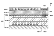
- FIG. 3 is a cross-sectional view of the imaging unit 40.
- the imaging unit 40 shown in FIG. 3 includes the glass slide 49, the imaging element 44, the FPC board 45, and the relay member 46 described above.
- the image sensor 44 is formed by a light receiving unit 441 that generates an image signal by receiving a subject image formed by the objective lenses 43a-1 to 43a-4 of the lens unit 43 and performing photoelectric conversion, and a light receiving unit 441.
- Semiconductor substrate 442, a through-via 443 (TSV: Through-Silicon Via) that propagates an image signal generated by the light receiving unit 441, and a bump that connects the through-via 443 and the FPC board 45 are provided on the semiconductor substrate 442. 444.
- the FPC board 45 includes a first board 451 connected to the back surface of the image sensor 44 via bumps 444, and a base end direction (extending direction of the signal cable 48) perpendicular to the first board 451 from one end of the first board 451. ) And a second substrate 452 that extends and bends so as to be continuous.
- the signal cable 48 is connected to the back surface 4521 of the second substrate 452.
- the relay member 46 is provided on the back side opposite to the image sensor 44 with respect to the light receiving portion 441 of the image sensor 44, and a plurality of silicon substrates 461 to 463 (stacked on the surface 4522 of the second substrate 452 of the FPC substrate 45). A semiconductor layer).
- Each of the plurality of silicon substrates 461 to 463 includes a plurality of electronic devices 4611, 4621, and 4631 formed in a planar shape.
- the plurality of electronic devices 4611, 4621, and 4631 are stacked in a direction (vertical direction) orthogonal to the extending direction of the signal cable 48 (see arrow A).
- Each of the electronic devices 4611, 4621, and 4631 is connected by at least an adjacent silicon substrate, specifically, a through via 464 that penetrates each layer.
- the plurality of electronic devices 4611, 4621, and 4631 are any of buffers, capacitors, inductors, and resistors that amplify the image signal generated by the imaging device 44 and output the amplified signal to the signal cable 48.
- a signal cable 48 is connected to the upper surface of the silicon substrate 463.
- the relay member 46 is provided on the back side with respect to the light receiving portion 441 of the image sensor 44, and the plurality of electronic devices 4611, 4621, and 4631 formed in a planar shape are provided. Since it is formed of the formed silicon substrates 461 to 463 and relays the image pickup element 44 and the signal cable 48, the image pickup unit 40 can be further reduced in size.
- the relay member 46 stacks the plurality of silicon substrates 461 to 463, whereby the image pickup unit 40 can be further reduced in size.
- a plurality of silicon substrates 461 to 463 are stacked in a direction parallel to the extending direction of the signal cable 48, and the signal cable 48 is connected to the relay member 46. Further downsizing of the imaging unit 40 can be realized.
- a plurality of silicon substrates 461 to 463 are stacked on the FPC substrate 45, and the signal cable 48 is connected to the back surface of the FPC substrate 45. Can be designed.
- the plurality of silicon substrates 461 to 463 are provided in the internal space of the distal end portion main body 41 of the insertion portion 30 in the endoscope 2, the distal end of the endoscope 2. Miniaturization of the part 3A can be realized.
- FIG. 4 is a cross-sectional view of the imaging unit according to Embodiment 2 of the present invention.
- An imaging unit 40a shown in FIG. 4 includes a glass slide 49, an imaging element 44, an FPC board 45a, a relay member 46a, and a passive element 100.
- the relay member 46a includes a plurality of silicon substrates 461a to 463a stacked on the back side opposite to the image sensor 44 with respect to the light receiving portion 441 of the image sensor 44.
- Each of the plurality of silicon substrates 461a to 463a has a plurality of electronic devices 4611, 4621, and 4631 formed in a planar shape.
- the area of each of the plurality of silicon substrates 461a to 463a is equal to or less than the projected area when the image sensor 44 is projected in the extending direction of the signal cable 48, and is stacked on the back side of the image sensor 44.
- the plurality of silicon substrates 461a to 463a are stacked in a direction parallel to the extending direction of the signal cable 48 (see arrow A).
- Each of the plurality of silicon substrates 461a to 463a is connected by a through via 464a penetrating each layer.
- the FPC board 45a includes a first board 451a connected to the back surface of the relay member 46a via a bump (not shown), and a base end direction (of the signal cable 48) perpendicular to the first board 451a from one end of the first board 451a.
- a second substrate 452a that extends and bends continuously in the extending direction.
- a signal cable 48 is connected to both surfaces 4521a and 4522a of the second substrate 452a of the FPC substrate 45a.
- the passive element 100 is connected to the back surface 4511a side of the first substrate 451a of the FPC substrate 45a.
- the passive element 100 is at least one of a chip capacitor, an inductor, and a resistor.
- the image pickup unit 40a is further provided. Miniaturization can be realized.
- the area of each of the plurality of silicon substrates 461a to 463a is stacked on the back side of the image sensor 44 below the projected area of the image sensor 44. Further downsizing can be realized.
- Modification 1 of the embodiment of the present invention differs in a structure from the relay member 46 which concerns on Embodiment 1 mentioned above.
- the relay member according to the first modification of the present embodiment forms planar electronic devices on both surfaces of each of a plurality of stacked silicon substrates. Below, the structure of the relay member which concerns on the modification 1 of this Embodiment is demonstrated.
- FIG. 5 is a cross-sectional view of a relay member according to Modification 1 of the embodiment of the present invention.
- the relay member 46b shown in FIG. 5 is formed by laminating a plurality of silicon substrates 461b, 462b, and 463b.
- Planar type electronic devices 4611b, 4612b, 4621b, 4622b, 4631b, and 4632b are formed on both surfaces of the plurality of silicon substrates 461b, 462b, and 463b, respectively. Further, each of the plurality of silicon substrates 461b, 462b, 463b is electrically connected by the through via 464b and the bumps 465a, 465b.
- the bump 465b is disposed at a position different from the vertical direction of the through via 464b, and may be connected to the silicon substrates 461b, 462b, 463b, or may be disposed at the same position as the vertical direction of the through via 464b, and the silicon substrates 461b, 462b. , 463b may be connected.
- a resin layer (not shown) may be formed in each gap between the plurality of silicon substrates 461b, 462b, and 463b to reinforce the connection strength between the silicon substrates.
- the electronic devices 4611b, 4612b, 4621b, 4622b, 4631b, and 4632b are any of a buffer, a capacitor, an inductor, and a resistor that amplify the image signal generated by the image sensor 44 and output the amplified signal to the signal cable 48.
- planar electronic devices 4611b, 4612b, 4621b, 4622b, 4631b, and 4632b are further formed on both surfaces of the silicon substrates 461b, 462b, and 463b. Miniaturization can be achieved.
- planar electronic devices 4611b, 4612b, 4621b, 4622b, 4631b, and 4632b are formed on both surfaces of the silicon substrates 461b, 462b, and 463b.
- a plurality of planar electronic devices may be formed in parallel on one surface of 462b.
- the second modification of the present embodiment is different only in the configuration of the relay member according to the first and second embodiments.
- the relay member according to the second modification of the present embodiment is formed by further laminating a multilayer wiring layer on a laminated silicon substrate. Below, the structure of the relay member which concerns on the modification 2 of this Embodiment is demonstrated.
- FIG. 6 is a cross-sectional view of a relay member according to Modification 2 of the embodiment of the present invention.
- the relay member 46c shown in FIG. 6 is formed by laminating a plurality of silicon substrates 461c, 462c, and 463c. Further, a multilayer wiring layer 465c is formed on the outermost layer of the silicon substrate 463c. Planar-type electronic devices 4611c, 4612c, 4621c, 4622c, 4631c, and 4632c are formed on both surfaces of each of the plurality of silicon substrates 461c, 462c, and 463c.
- each of the plurality of silicon substrates 461c, 462c, 463c and the multilayer wiring layer 465c is electrically connected by a through via 464c.
- the planar electronic devices 4611c, 4612c, 4621c, 4622c, 4631c, and 4632c are connected without using bumps by directly joining the through vias 464c.
- the electronic devices 4611c, 4612c, 4621c, 4622c, 4631c, and 4632c are any of a buffer, a capacitor, an inductor, and a resistor that amplify the image signal generated by the imaging device 44 and output the amplified signal to the signal cable 48.
- a material capable of connecting an electronic component or a signal cable by solder for example, an electrode in which an Au plating layer is formed on a Cu layer via a Ni barrier layer is formed.
- solder for example, an electrode in which an Au plating layer is formed on a Cu layer via a Ni barrier layer is formed.
- another electronic component, a passive element, and the signal cable 48 can be connected with solder.
- a multilayer FPC substrate may be stacked as the multilayer wiring layer 465c, or may be formed on the silicon substrate 463c by a known build-up method.
- high-density wiring can be performed by forming the multilayer wiring layer 465c on the outermost layer of the silicon substrate 463c.
- the multilayer wiring layer 465c on the outermost layer of the silicon substrate 463c, other electronic components, passive elements and the signal cable 48 are soldered. Can be connected.
- planar electronic devices 4611c, 4612c, 4621c, 4622c, 4631c, and 4632c are provided on both surfaces of each of the plurality of silicon substrates 461c, 462c, and 463c. By forming, further miniaturization can be achieved.
- the third modification of the present embodiment is different in configuration from the imaging unit 40 according to the first embodiment described above.
- the imaging unit according to Modification 3 of the present embodiment is configured using a front side illumination type imaging device (imager chip), and a relay unit is stacked on the back surface of the imaging device. To do.
- the configuration of the imaging unit according to Modification 3 of the present embodiment will be described.
- FIG. 7 is a schematic diagram of a cross section of an imaging unit according to Modification 3 of the embodiment of the present invention.
- the image pickup unit 40d shown in FIG. 7 receives the light and performs photoelectric conversion to generate an image signal (electric signal) 44d, a relay member 46d that relays the image pickup element 44d and the signal cable 48, Is provided.
- the image pickup element 44d is a semiconductor substrate 441d on which a light receiving portion (pixel portion) in which a plurality of pixels (photodiodes) that output electric signals by receiving light and performing photoelectric conversion are arranged in a two-dimensional matrix is formed.
- the relay member 46d includes a semiconductor substrate 461d (silicon substrate) on which a circuit or the like is formed, an electronic device layer 462d formed by laminating a dielectric or the like on the semiconductor substrate 461d, and an outermost layer of the electronic device layer 462d. And a connection portion 463d that connects to the image sensor 44d.
- the electronic device layer 462d is either a buffer that amplifies and outputs an image signal output from the image sensor 44d, or a bypass capacitor that passes an AC component such as noise to the ground.
- the electronic device layer 462d includes an electrode 465d.
- the electrode 465d is electrically connected to the through via 443d through the through via 464d and the bump 444d.
- the back side of the semiconductor substrate 441d of the image sensor 44d and the back side of the semiconductor substrate 461d of the relay member 46d may be connected and stacked.
- the semiconductor substrate 461d is electrically connected to the semiconductor substrate 441d via the bumps 444d and the through vias 443d.
- the fourth modification of the present embodiment is different in configuration from the imaging unit 40 according to the first embodiment described above.
- the imaging unit according to Modification 4 of the present embodiment is configured using a back side illumination type imaging device (imager chip), and a relay unit is stacked on the back surface of the imaging device. To do.
- the configuration of the imaging unit according to Modification 4 of the present embodiment will be described.
- FIG. 9 is a schematic diagram of a cross section of an imaging unit according to Modification 4 of the embodiment of the present invention.
- An imaging unit 40f illustrated in FIG. 9 includes an imaging element 44f that generates an image signal (electric signal) by receiving light and performing photoelectric conversion, and the relay member 46d of the third modification of the above-described embodiment. Prepare.
- the image pickup element 44f receives a light and performs photoelectric conversion to output a semiconductor signal 441d on which a light receiving portion (pixel portion) in which a plurality of pixels (photodiodes) that output electric signals are arranged in a two-dimensional matrix is formed.
- a wiring layer 442d stacked on the semiconductor substrate 441d, and a through via 443d.
- the imaging element 44f is electrically connected to the relay member 46d through the through via 443d and the bump 444d.
- the relay member 46d is stacked on the back surface of the image pickup device 44d, so that the image pickup unit 40f can be further downsized.
- the front side of the light receiving part 442d of the image sensor 44f and the back side of the semiconductor substrate 461d of the relay member 46d may be connected and stacked.
- the front side of the light receiving portion 442d (wiring layer) of the imaging element 44f and the back side of the semiconductor substrate 461d of the relay member 46d are electrically connected via bumps 444d. The Thereby, further miniaturization can be achieved.
- the present invention can include various embodiments not described herein, and various design changes can be made within the scope of the technical idea specified by the claims. It is.
Abstract
Provided are an imaging unit and an endoscope that can be made more compact. An imaging unit 40 comprises an imaging element 44 that generates an image signal by photoelectrically converting received light and an interposer 46, which provides a relay between the imaging unit 44 and a signal cable 48 that transmits the image signal, and which is provided on the back surface side of the imaging element 44, said back surface side being the opposite side from the light-receiving surface of the imaging element 44. The interposer 46 comprises silicon substrates 461, 462, 463 on which planar electronic devices 4611, 4621, 4631 have been formed.
Description
本発明は、被検体に挿入され、被検体内の体内を撮像して該体内の画像データを生成する撮像ユニット、該撮像ユニットを先端部に備えた内視鏡に関する。
The present invention relates to an imaging unit that is inserted into a subject and images the inside of the subject to generate image data in the body, and an endoscope that includes the imaging unit at a distal end portion.
従来、内視鏡は、先端に撮像装置が設けられた細長形状をなす可撓性の挿入部を患者等の被検体内に挿入することによって、被検体内の体内画像を取得する。このような内視鏡において使用される撮像ユニットは、撮像素子が形成された半導体チップと、この半導体チップの背面側に隣接して配置され、撮像素子の駆動回路を構成するコンデンサ、抵抗およびICチップ等の電子部品が実装された回路基板と、を備える(特許文献1,2を参照)。
Conventionally, an endoscope acquires an in-vivo image in a subject by inserting a flexible insertion portion having an elongated shape with an imaging device provided at the tip into the subject such as a patient. An imaging unit used in such an endoscope includes a semiconductor chip on which an imaging element is formed, and a capacitor, a resistor, and an IC that are arranged adjacent to the back side of the semiconductor chip and constitute a driving circuit for the imaging element. And a circuit board on which electronic components such as chips are mounted (see Patent Documents 1 and 2).
しかしながら、上述した特許文献1,2では、コンデンサ、抵抗およびICチップ等の電子部品が半導体チップの背面から信号ケーブルの延出方向に設けられているため、撮像ユニットが縦長になってしまう。このため、患者の負担をさらに軽減するため、より一層の小型化が求められていた。
However, in Patent Documents 1 and 2 described above, the electronic unit such as a capacitor, a resistor, and an IC chip are provided in the extending direction of the signal cable from the back surface of the semiconductor chip. For this reason, in order to further reduce the burden on the patient, further downsizing has been demanded.
本発明は、上記に鑑みてなされたものであって、さらなる小型化を実現することができる撮像ユニットおよび内視鏡を提供することを目的とする。
The present invention has been made in view of the above, and an object thereof is to provide an imaging unit and an endoscope that can realize further downsizing.
上述した課題を解決し、目的を達成するために、本発明に係る撮像ユニットは、光を受光して光電変換を行うことによって画像信号を生成する撮像素子と、前記撮像素子の受光面に対する前記撮像素子の反対側である背面側に設けられ、プレーナ型の電子デバイスが形成されたシリコン基板を有し、前記撮像素子と前記画像信号を伝送する信号ケーブルとを中継する中継部材と、を備えたことを特徴とする。
In order to solve the above-described problems and achieve the object, an imaging unit according to the present invention includes an imaging element that generates light by receiving light and performing photoelectric conversion, and the light receiving surface of the imaging element. A relay member provided on the back side opposite to the image sensor, having a silicon substrate on which a planar electronic device is formed, and relaying the image sensor and a signal cable for transmitting the image signal; It is characterized by that.
また、本発明に係る撮像ユニットは、上記発明において、前記中継部材は、複数の前記シリコン基板が積層されていることを特徴とする。
Further, the imaging unit according to the present invention is characterized in that, in the above invention, the relay member is formed by laminating a plurality of the silicon substrates.
また、本発明に係る撮像ユニットは、上記発明において、複数の前記シリコン基板は、前記信号ケーブルの延出方向と直交する方向に積層されていることを特徴とする。
The imaging unit according to the present invention is characterized in that, in the above invention, the plurality of silicon substrates are stacked in a direction orthogonal to the extending direction of the signal cable.
また、本発明に係る撮像ユニットは、上記発明において、前記中継部材は、前記信号ケーブルの延出方向と平行に延出するフレキシブルプリント基板をさらに有し、複数の前記シリコン基板は、前記フレキシブルプリント基板に積層されることを特徴とする。
In the imaging unit according to the present invention, in the above invention, the relay member further includes a flexible printed circuit board extending in parallel with an extending direction of the signal cable, and the plurality of silicon substrates include the flexible printed circuit. It is characterized by being laminated on a substrate.
また、本発明に係る撮像ユニットは、上記発明において、複数の前記シリコン基板は、前記信号ケーブルの延出方向と平行な方向に積層されることを特徴とする。
The imaging unit according to the present invention is characterized in that, in the above invention, the plurality of silicon substrates are stacked in a direction parallel to an extending direction of the signal cable.
また、本発明に係る撮像ユニットは、上記発明において、複数の前記シリコン基板の各々の面積は、前記撮像素子を前記信号ケーブルの延出方向へ投影したときの投影面積以下であることを特徴とする。
In the imaging unit according to the present invention, the area of each of the plurality of silicon substrates is not more than a projected area when the imaging element is projected in the extending direction of the signal cable. To do.
また、本発明に係る撮像ユニットは、上記発明において、複数の前記シリコン基板は、少なくとも隣接するシリコン基板を貫通する貫通ビアによって接続されていることを特徴とする。
The imaging unit according to the present invention is characterized in that, in the above invention, the plurality of silicon substrates are connected by a through via penetrating at least an adjacent silicon substrate.
また、本発明に係る撮像ユニットは、上記発明において、複数の前記シリコン基板の各々は、両面に前記電子デバイスが形成されていることを特徴とする。
Further, the imaging unit according to the present invention is characterized in that, in the above invention, each of the plurality of silicon substrates has the electronic device formed on both sides.
また、本発明に係る撮像ユニットは、上記発明において、前記電子デバイスは、バッファ、コンデンサ、インダクタおよび抵抗の少なくとも一つであることを特徴とする。
In the imaging unit according to the present invention as set forth in the invention described above, the electronic device is at least one of a buffer, a capacitor, an inductor, and a resistor.
また、本発明に係る内視鏡は、上記発明の撮像ユニットと、硬質部材によって形成された筒状をなす先端部を有し、被検体内に挿入可能な挿入部と、を備え、前記挿入部は、前記先端部の内部空間に前記撮像ユニットを有することを特徴とする。
An endoscope according to the present invention includes the imaging unit according to the invention described above, and an insertion portion having a cylindrical tip formed by a hard member and insertable into a subject. The unit includes the imaging unit in an internal space of the tip.
本発明によれば、さらなる小型化を実現することができるという効果を奏する。
According to the present invention, there is an effect that further downsizing can be realized.
以下、本発明を実施するための形態(以下、「実施の形態」という)として、撮像装置を備えた内視鏡について説明する。また、この実施の形態により本発明が限定されるものではない。さらに、以下の説明において参照する各図は、本発明の内容を理解でき得る程度に形状、大きさ、および位置関係を概略的に示してあるに過ぎない。すなわち、本発明は、各図で例示された形状、大きさおよび位置関係のみに限定されるものではない。さらにまた、図面の相互間においても、互いの寸法や比率が異なる部分が含まれている。
Hereinafter, an endoscope provided with an imaging device will be described as a mode for carrying out the present invention (hereinafter referred to as “embodiment”). Further, the present invention is not limited by this embodiment. Further, the drawings referred to in the following description only schematically show the shape, size, and positional relationship so that the contents of the present invention can be understood. That is, the present invention is not limited only to the shape, size, and positional relationship illustrated in each drawing. Furthermore, the drawings include portions having different dimensions and ratios.
(実施の形態1)
〔内視鏡システムの構成〕
図1は、本発明の実施の形態1に係る内視鏡システムの全体構成を模式的に示す図である。図1に示す内視鏡システム1は、内視鏡2と、ユニバーサルコード3(伝送ケーブル)と、コネクタ部5と、プロセッサ6(制御装置)と、表示装置7と、光源装置8と、を備える。 (Embodiment 1)
[Configuration of endoscope system]
FIG. 1 is a diagram schematically showing an overall configuration of an endoscope system according toEmbodiment 1 of the present invention. An endoscope system 1 shown in FIG. 1 includes an endoscope 2, a universal cord 3 (transmission cable), a connector unit 5, a processor 6 (control device), a display device 7, and a light source device 8. Prepare.
〔内視鏡システムの構成〕
図1は、本発明の実施の形態1に係る内視鏡システムの全体構成を模式的に示す図である。図1に示す内視鏡システム1は、内視鏡2と、ユニバーサルコード3(伝送ケーブル)と、コネクタ部5と、プロセッサ6(制御装置)と、表示装置7と、光源装置8と、を備える。 (Embodiment 1)
[Configuration of endoscope system]
FIG. 1 is a diagram schematically showing an overall configuration of an endoscope system according to
内視鏡2は、挿入部30を被検体内に挿入することによって、被検体の体内画像を撮像して画像信号(画像データ)をプロセッサ6へ出力する。ユニバーサルコード3の内部の電気ケーブルの束は、内視鏡2の挿入部30まで延伸され、挿入部30の先端部3Aに設けられた撮像装置に接続する。内視鏡2の挿入部30の基端側には、内視鏡機能を操作する各種ボタン類やノブ類が設けられた操作部4が接続される。操作部4は、被検体の体腔内に生体鉗子、電気メスおよび検査プローブ等の処置具を挿入する処置具挿入口4aを有する。
The endoscope 2 captures an in-vivo image of the subject by inserting the insertion unit 30 into the subject, and outputs an image signal (image data) to the processor 6. The bundle of electric cables inside the universal cord 3 extends to the insertion portion 30 of the endoscope 2 and is connected to an imaging device provided at the distal end portion 3A of the insertion portion 30. An operation unit 4 provided with various buttons and knobs for operating the endoscope function is connected to the proximal end side of the insertion unit 30 of the endoscope 2. The operation unit 4 has a treatment instrument insertion port 4a for inserting a treatment instrument such as a biological forceps, an electric knife, and an inspection probe into the body cavity of the subject.
コネクタ部5は、ユニバーサルコード3の基端に設けられ、プロセッサ6および光源装置8に接続される。コネクタ部5は、ユニバーサルコード3と接続する先端部3Aの撮像装置が出力する画像信号に所定の信号処理を施すとともに、この画像信号にA/D変換を行ってデジタルの画像信号をプロセッサ6へ出力する。
The connector unit 5 is provided at the base end of the universal cord 3 and is connected to the processor 6 and the light source device 8. The connector unit 5 performs predetermined signal processing on the image signal output from the imaging device of the distal end portion 3 </ b> A connected to the universal cord 3, and performs A / D conversion on the image signal to send the digital image signal to the processor 6. Output.
プロセッサ6は、コネクタ部5から出力された画像信号に所定の画像処理を施すとともに、この画像信号を表示装置7へ出力する。また、プロセッサ6は、内視鏡システム1全体を制御する。プロセッサ6は、CPU(Central Processing Unit)等を用いて構成される。
The processor 6 performs predetermined image processing on the image signal output from the connector unit 5 and outputs the image signal to the display device 7. The processor 6 controls the entire endoscope system 1. The processor 6 is configured using a CPU (Central Processing Unit) or the like.
表示装置7は、プロセッサ6から出力された画像信号に対応する画像を表示する。表示装置7は、液晶または有機EL(Electro Luminescence)等の表示パネル等を用いて構成される。
The display device 7 displays an image corresponding to the image signal output from the processor 6. The display device 7 is configured using a display panel such as liquid crystal or organic EL (Electro Luminescence).
光源装置8は、コネクタ部5およびユニバーサルコード3を経由して内視鏡2の挿入部30の先端から被写体に向けて照明光を照射する。光源装置8は、キセノンランプやLED(Light Emitting Diode)ランプ等を用いて構成される。
The light source device 8 irradiates illumination light from the distal end of the insertion portion 30 of the endoscope 2 toward the subject via the connector portion 5 and the universal cord 3. The light source device 8 is configured using a xenon lamp, an LED (Light Emitting Diode) lamp, or the like.
挿入部30は、撮像装置が設けられた先端部3Aと、先端部3Aの基端側に連設された複数方向に湾曲自在な湾曲部3Bと、この湾曲部3Bの基端側に連設された可撓管部3Cと、を有する。先端部3Aに設けられた撮像装置が撮像した画像信号は、例えば数mの長さを有するユニバーサルコード3により、操作部4を介してコネクタ部5に接続される。湾曲部3Bは、操作部4に設けられた湾曲操作用ノブ4bの操作によって湾曲し、挿入部30内部に挿通された湾曲ワイヤの牽引弛緩にともない、例えば上下左右の4方向に湾曲自在である。
The insertion portion 30 includes a distal end portion 3A provided with an imaging device, a bending portion 3B that is connected to the proximal end side of the distal end portion 3A and is bendable in a plurality of directions, and a proximal end side of the bending portion 3B. Flexible tube portion 3C. An image signal captured by the imaging device provided at the distal end portion 3A is connected to the connector portion 5 via the operation portion 4 by, for example, a universal cord 3 having a length of several meters. The bending portion 3B is bent by the operation of the bending operation knob 4b provided in the operation portion 4, and can be bent in, for example, four directions, up, down, left, and right, as the bending wire inserted into the insertion portion 30 is pulled or loosened. .
また、内視鏡2は、光源装置8からの照明光を伝搬するためのライトガイド(不図示)が設けられ、このライトガイドによる照明光の出射端に照明レンズ(不図示)が設けられている。この照明レンズは、挿入部30の先端部3Aに設けられている。
Further, the endoscope 2 is provided with a light guide (not shown) for propagating illumination light from the light source device 8, and an illumination lens (not shown) is provided at the exit end of the illumination light by the light guide. Yes. This illumination lens is provided at the distal end portion 3 </ b> A of the insertion portion 30.
〔内視鏡の先端部の構成〕
次に、内視鏡2の先端部3Aの構成について詳細に説明する。図2は、内視鏡2の先端部3Aの部分断面図であり、内視鏡2の先端部3Aに設けられた撮像装置の基板面に対して直交する面であって、撮像装置の光軸方向と平行な面で切断した場合の部分断面である。また、図2においては、内視鏡2の挿入部30の先端部3Aと湾曲部3Bの一部を図示する。 [Configuration of the tip of the endoscope]
Next, the configuration of thedistal end portion 3A of the endoscope 2 will be described in detail. FIG. 2 is a partial cross-sectional view of the distal end portion 3A of the endoscope 2, which is a surface orthogonal to the substrate surface of the imaging device provided at the distal end portion 3A of the endoscope 2, and shows light from the imaging device. It is a partial cross section at the time of cut | disconnecting in a surface parallel to an axial direction. Further, FIG. 2 illustrates a part of the distal end portion 3A and the bending portion 3B of the insertion portion 30 of the endoscope 2.
次に、内視鏡2の先端部3Aの構成について詳細に説明する。図2は、内視鏡2の先端部3Aの部分断面図であり、内視鏡2の先端部3Aに設けられた撮像装置の基板面に対して直交する面であって、撮像装置の光軸方向と平行な面で切断した場合の部分断面である。また、図2においては、内視鏡2の挿入部30の先端部3Aと湾曲部3Bの一部を図示する。 [Configuration of the tip of the endoscope]
Next, the configuration of the
図2に示すように、湾曲部3Bは、後述する被覆管42の内側に設けられた湾曲管81内部に挿通された湾曲ワイヤ82の牽引弛緩にともない、上下左右の4方向に湾曲自在である。この湾曲部3Bの先端側に延設された先端部3Aの内部に、撮像装置35が設けられている。
As shown in FIG. 2, the bending portion 3 </ b> B can be bent in four directions, up, down, left, and right as the bending wire 82 inserted into the bending tube 81 provided inside the cladding tube 42 described later is pulled and loosened. . An imaging device 35 is provided inside the distal end portion 3A extending to the distal end side of the curved portion 3B.
撮像装置35は、レンズユニット43と、レンズユニット43の基端側に配置された撮像ユニット40と、を有する。撮像装置35は、接着剤41aによって先端部本体41の内側に接着される。先端部本体41は、撮像装置35を収容する内部空間k1を形成するための硬質部材等によって筒状に形成される。先端部本体41の基端側外周部41bは、柔軟な被覆管42によって被覆される。先端部本体41よりも基端側の部材は、湾曲部3Bが湾曲可能なように柔軟な部材によって形成される。先端部本体41が配置される先端部3Aが挿入部30の硬質部分となる。
The imaging device 35 includes a lens unit 43 and an imaging unit 40 disposed on the base end side of the lens unit 43. The imaging device 35 is bonded to the inside of the tip end body 41 by an adhesive 41a. The tip portion main body 41 is formed in a cylindrical shape by a hard member or the like for forming an internal space k1 that accommodates the imaging device 35. The proximal end side outer peripheral portion 41 b of the distal end portion main body 41 is covered with a flexible cladding tube 42. The member on the base end side with respect to the distal end portion main body 41 is formed of a flexible member so that the bending portion 3B can be bent. 3 A of front-end | tip parts in which the front-end | tip part main body 41 is arrange | positioned become a hard part of the insertion part 30. FIG.
レンズユニット43は、複数の対物レンズ43a-1~43a-4と、複数の対物レンズ43a-1~43a-4を保持するレンズホルダ43bと、を有する。レンズユニット43は、レンズホルダ43bの先端が先端部本体41の内部に挿嵌固定されることによって、先端部本体41に固定される。複数の対物レンズ43a-1~43a-4は、被写体像を結像する。
The lens unit 43 includes a plurality of objective lenses 43a-1 to 43a-4 and a lens holder 43b that holds the plurality of objective lenses 43a-1 to 43a-4. The lens unit 43 is fixed to the tip portion main body 41 by inserting and fixing the tip of the lens holder 43 b inside the tip portion main body 41. The plurality of objective lenses 43a-1 to 43a-4 form a subject image.
撮像ユニット40は、CCD(Charge Coupled Device)またはCMOS(Complementary Metal Oxide Semiconductor)等の光を受光して光電変換を行うことによって電気信号(画像信号)を生成する受光部を有する撮像素子44と、撮像素子44の受光面の裏側から光軸方向に延出するフレキシブルプリント基板45(以下、「FPC基板45」という)と、FPC基板45の表面に積層されるとともに、プレーナ型の電子デバイスが形成されたシリコン基板からなり、撮像素子44と電気ケーブル束47の各信号ケーブル48とを中継する中継部材46(インタポーザ)と、撮像素子44の受光面を覆った状態で撮像素子44に接着するガラススリッド49と、を備える。なお、撮像ユニット40の詳細な構成は、後述する。
The imaging unit 40 includes an imaging element 44 having a light receiving unit that generates an electric signal (image signal) by receiving light such as a CCD (Charge Coupled Device) or CMOS (Complementary Metal Oxide Semiconductor) and performing photoelectric conversion. A flexible printed circuit board 45 (hereinafter referred to as “FPC board 45”) extending in the direction of the optical axis from the back side of the light receiving surface of the image sensor 44, and a planar electronic device are formed on the surface of the FPC board 45. A relay member 46 (interposer) that relays between the image sensor 44 and each signal cable 48 of the electric cable bundle 47, and a glass that adheres to the image sensor 44 while covering the light receiving surface of the image sensor 44. And a slide 49. The detailed configuration of the imaging unit 40 will be described later.
信号ケーブル48は、基端が挿入部30の基端方向に延伸する。電気ケーブル束47は、挿入部30に挿通可能に先端部本体41に配置され、図1に示す操作部4およびユニバーサルコード3を介してコネクタ部5まで延設されている。
The base end of the signal cable 48 extends in the base end direction of the insertion portion 30. The electric cable bundle 47 is disposed on the distal end portion body 41 so as to be able to be inserted into the insertion portion 30 and extends to the connector portion 5 via the operation portion 4 and the universal cord 3 shown in FIG.
レンズユニット43の対物レンズ43a-1~43a-4によって結像された被写体像は、対物レンズ43a-1~43a-4の結像位置に配設された撮像素子44によって受光されて光電変換されることによって、画像信号に変換される。撮像素子44によって生成された画像信号は、FPC基板45、中継部材46および中継部材46に接続する信号ケーブル48およびコネクタ部5を経由して、プロセッサ6に出力される。
The subject image formed by the objective lenses 43a-1 to 43a-4 of the lens unit 43 is received and photoelectrically converted by the image pickup device 44 provided at the imaging positions of the objective lenses 43a-1 to 43a-4. Thus, it is converted into an image signal. The image signal generated by the image sensor 44 is output to the processor 6 via the FPC board 45, the relay member 46, the signal cable 48 connected to the relay member 46, and the connector unit 5.
撮像装置35および電気ケーブル束47の先端部は、耐性向上のために、熱収縮チューブ50によって外周が被覆される。熱収縮チューブ50の内部は、封止樹脂51によって部品間の隙間が充填されている。
The outer ends of the imaging device 35 and the electric cable bundle 47 are covered with a heat shrinkable tube 50 in order to improve resistance. The inside of the heat shrinkable tube 50 is filled with a gap between components by the sealing resin 51.
〔撮像ユニットの詳細な構成〕
次に、撮像ユニット40について詳細に説明する。図3は、撮像ユニット40の断面図である。図3に示す撮像ユニット40は、上述したガラススリッド49と、撮像素子44と、FPC基板45と、中継部材46と、を備える。 [Detailed configuration of imaging unit]
Next, theimaging unit 40 will be described in detail. FIG. 3 is a cross-sectional view of the imaging unit 40. The imaging unit 40 shown in FIG. 3 includes the glass slide 49, the imaging element 44, the FPC board 45, and the relay member 46 described above.
次に、撮像ユニット40について詳細に説明する。図3は、撮像ユニット40の断面図である。図3に示す撮像ユニット40は、上述したガラススリッド49と、撮像素子44と、FPC基板45と、中継部材46と、を備える。 [Detailed configuration of imaging unit]
Next, the
撮像素子44は、レンズユニット43の対物レンズ43a-1~43a-4によって結像された被写体像を受光して光電変換を行うことによって画像信号を生成する受光部441と、受光部441が形成された半導体基板442と、半導体基板442に設けられ、受光部441が生成した画像信号を伝搬する貫通ビア443(TSV:Through-Silicon Via)と、貫通ビア443とFPC基板45とを接続するバンプ444と、を有する。
The image sensor 44 is formed by a light receiving unit 441 that generates an image signal by receiving a subject image formed by the objective lenses 43a-1 to 43a-4 of the lens unit 43 and performing photoelectric conversion, and a light receiving unit 441. Semiconductor substrate 442, a through-via 443 (TSV: Through-Silicon Via) that propagates an image signal generated by the light receiving unit 441, and a bump that connects the through-via 443 and the FPC board 45 are provided on the semiconductor substrate 442. 444.
FPC基板45は、撮像素子44の裏面にバンプ444を介して接続される第1基板451と、第1基板451の一端から第1基板451と直交する基端方向(信号ケーブル48の延出方向)に連続して連なるように延在して折り曲げられた第2基板452と、を有する。また、第2基板452の背面4521には、信号ケーブル48が接続される。
The FPC board 45 includes a first board 451 connected to the back surface of the image sensor 44 via bumps 444, and a base end direction (extending direction of the signal cable 48) perpendicular to the first board 451 from one end of the first board 451. ) And a second substrate 452 that extends and bends so as to be continuous. The signal cable 48 is connected to the back surface 4521 of the second substrate 452.
中継部材46は、撮像素子44の受光部441に対する撮像素子44の反対側である背面側に設けられ、FPC基板45の第2基板452の表面4522に積層された複数のシリコン基板461~463(半導体層)を有する。複数のシリコン基板461~463の各々は、プレーナ型で形成された複数の電子デバイス4611,4621,4631を有する。複数の電子デバイス4611,4621,4631は、信号ケーブル48の延出方向(矢印Aを参照)と直交する方向(垂直方向)に積層される。電子デバイス4611,4621,4631の各々は、少なくとも隣接するシリコン基板、具体的には各層を貫通する貫通ビア464によって接続される。複数の電子デバイス4611,4621,4631は、撮像素子44が生成した画像信号を増幅して信号ケーブル48へ出力するバッファ、コンデンサ、インダクタおよび抵抗のいずれかである。また、シリコン基板463の上面には、信号ケーブル48が接続される。
The relay member 46 is provided on the back side opposite to the image sensor 44 with respect to the light receiving portion 441 of the image sensor 44, and a plurality of silicon substrates 461 to 463 (stacked on the surface 4522 of the second substrate 452 of the FPC substrate 45). A semiconductor layer). Each of the plurality of silicon substrates 461 to 463 includes a plurality of electronic devices 4611, 4621, and 4631 formed in a planar shape. The plurality of electronic devices 4611, 4621, and 4631 are stacked in a direction (vertical direction) orthogonal to the extending direction of the signal cable 48 (see arrow A). Each of the electronic devices 4611, 4621, and 4631 is connected by at least an adjacent silicon substrate, specifically, a through via 464 that penetrates each layer. The plurality of electronic devices 4611, 4621, and 4631 are any of buffers, capacitors, inductors, and resistors that amplify the image signal generated by the imaging device 44 and output the amplified signal to the signal cable 48. A signal cable 48 is connected to the upper surface of the silicon substrate 463.
以上説明した本発明の実施の形態1によれば、中継部材46が撮像素子44の受光部441に対して背面側に設けられ、プレーナ型で形成された複数の電子デバイス4611,4621,4631が形成されたシリコン基板461~463からなり、撮像素子44と信号ケーブル48とを中継するので、撮像ユニット40のさらなる小型化を実現することができる。
According to the first embodiment of the present invention described above, the relay member 46 is provided on the back side with respect to the light receiving portion 441 of the image sensor 44, and the plurality of electronic devices 4611, 4621, and 4631 formed in a planar shape are provided. Since it is formed of the formed silicon substrates 461 to 463 and relays the image pickup element 44 and the signal cable 48, the image pickup unit 40 can be further reduced in size.
また、本発明の実施の形態1によれば、中継部材46が複数のシリコン基板461~463を積層することによって、撮像ユニット40のさらなる小型化を実現することができる。
Further, according to the first embodiment of the present invention, the relay member 46 stacks the plurality of silicon substrates 461 to 463, whereby the image pickup unit 40 can be further reduced in size.
さらに、本発明の実施の形態1によれば、複数のシリコン基板461~463が信号ケーブル48の延出方向と平行な方向に積層され、この信号ケーブル48が中継部材46に接続されるので、撮像ユニット40のさらなる小型化を実現することができる。
Furthermore, according to the first embodiment of the present invention, a plurality of silicon substrates 461 to 463 are stacked in a direction parallel to the extending direction of the signal cable 48, and the signal cable 48 is connected to the relay member 46. Further downsizing of the imaging unit 40 can be realized.
さらにまた、本発明の実施の形態1によれば、複数のシリコン基板461~463がFPC基板45に積層し、FPC基板45の裏面に信号ケーブル48を接続しているので、自由度を持たせた設計を行うことができる。
Furthermore, according to the first embodiment of the present invention, a plurality of silicon substrates 461 to 463 are stacked on the FPC substrate 45, and the signal cable 48 is connected to the back surface of the FPC substrate 45. Can be designed.
また、本発明の実施の形態1によれば、複数のシリコン基板461~463が内視鏡2における挿入部30の先端部本体41の内部空間に設けられているので、内視鏡2の先端部3Aの小型化を実現することができる。
Further, according to the first embodiment of the present invention, since the plurality of silicon substrates 461 to 463 are provided in the internal space of the distal end portion main body 41 of the insertion portion 30 in the endoscope 2, the distal end of the endoscope 2. Miniaturization of the part 3A can be realized.
(実施の形態2)
次に、本発明の実施の形態2について説明する。本実施の形態2は、上述した実施の形態1に係る撮像ユニット40のみが異なる。以下においては、本実施の形態2に係る撮像ユニットについて説明する。なお、上述した実施の形態1に係る内視鏡システム1と同一の構成には同一の符号を付して説明を省略する。 (Embodiment 2)
Next, a second embodiment of the present invention will be described. The second embodiment is different only in theimaging unit 40 according to the first embodiment described above. Hereinafter, the imaging unit according to the second embodiment will be described. In addition, the same code | symbol is attached | subjected to the structure same as the endoscope system 1 which concerns on Embodiment 1 mentioned above, and description is abbreviate | omitted.
次に、本発明の実施の形態2について説明する。本実施の形態2は、上述した実施の形態1に係る撮像ユニット40のみが異なる。以下においては、本実施の形態2に係る撮像ユニットについて説明する。なお、上述した実施の形態1に係る内視鏡システム1と同一の構成には同一の符号を付して説明を省略する。 (Embodiment 2)
Next, a second embodiment of the present invention will be described. The second embodiment is different only in the
〔撮像ユニットの詳細な構成〕
図4は、本発明の実施の形態2に係る撮像ユニットの断面図である。図4に示す撮像ユニット40aは、ガラススリッド49と、撮像素子44と、FPC基板45aと、中継部材46aと、受動素子100と、を備える。 [Detailed configuration of imaging unit]
FIG. 4 is a cross-sectional view of the imaging unit according toEmbodiment 2 of the present invention. An imaging unit 40a shown in FIG. 4 includes a glass slide 49, an imaging element 44, an FPC board 45a, a relay member 46a, and a passive element 100.
図4は、本発明の実施の形態2に係る撮像ユニットの断面図である。図4に示す撮像ユニット40aは、ガラススリッド49と、撮像素子44と、FPC基板45aと、中継部材46aと、受動素子100と、を備える。 [Detailed configuration of imaging unit]
FIG. 4 is a cross-sectional view of the imaging unit according to
中継部材46aは、撮像素子44の受光部441に対する撮像素子44の反対側である背面側に積層された複数のシリコン基板461a~463aを有する。複数のシリコン基板461a~463aの各々は、プレーナ型で形成された複数の電子デバイス4611,4621,4631を有する。複数のシリコン基板461a~463aの各々の面積は、撮像素子44を信号ケーブル48の延出方向へ投影したときの投影面積以下で撮像素子44の背面側に積層される。複数のシリコン基板461a~463aは、信号ケーブル48の延出方向(矢印Aを参照)と平行な方向に積層される。複数のシリコン基板461a~463aの各々は、各層を貫通する貫通ビア464aによって接続される。
The relay member 46a includes a plurality of silicon substrates 461a to 463a stacked on the back side opposite to the image sensor 44 with respect to the light receiving portion 441 of the image sensor 44. Each of the plurality of silicon substrates 461a to 463a has a plurality of electronic devices 4611, 4621, and 4631 formed in a planar shape. The area of each of the plurality of silicon substrates 461a to 463a is equal to or less than the projected area when the image sensor 44 is projected in the extending direction of the signal cable 48, and is stacked on the back side of the image sensor 44. The plurality of silicon substrates 461a to 463a are stacked in a direction parallel to the extending direction of the signal cable 48 (see arrow A). Each of the plurality of silicon substrates 461a to 463a is connected by a through via 464a penetrating each layer.
FPC基板45aは、中継部材46aの裏面にバンプ(不図示)を介して接続される第1基板451aと、第1基板451aの一端から第1基板451aと直交する基端方向(信号ケーブル48の延出方向)に連続して連なるように延在して折り曲げられた第2基板452aと、を有する。また、FPC基板45aの第2基板452aの両面4521a,4522aには、信号ケーブル48がそれぞれ接続される。
The FPC board 45a includes a first board 451a connected to the back surface of the relay member 46a via a bump (not shown), and a base end direction (of the signal cable 48) perpendicular to the first board 451a from one end of the first board 451a. A second substrate 452a that extends and bends continuously in the extending direction. A signal cable 48 is connected to both surfaces 4521a and 4522a of the second substrate 452a of the FPC substrate 45a.
受動素子100は、FPC基板45aの第1基板451aの背面4511a側に接続される。受動素子100は、チップコンデンサ、インダクタおよび抵抗の少なくとも1つである。
The passive element 100 is connected to the back surface 4511a side of the first substrate 451a of the FPC substrate 45a. The passive element 100 is at least one of a chip capacitor, an inductor, and a resistor.
以上説明した本発明の実施の形態2によれば、複数のシリコン基板461a~463aが信号ケーブル48の延出方向(矢印Aを参照)と平行な方向に積層されるので、撮像ユニット40aのさらなる小型化を実現することができる。
According to the second embodiment of the present invention described above, since the plurality of silicon substrates 461a to 463a are stacked in a direction parallel to the extending direction of the signal cable 48 (see arrow A), the image pickup unit 40a is further provided. Miniaturization can be realized.
さらに、本発明の実施の形態2によれば、複数のシリコン基板461a~463aの各々の面積は、撮像素子44の投影面積以下で撮像素子44の背面側に積層されるので、撮像ユニット40aのさらなる小型化を実現することができる。
Furthermore, according to the second embodiment of the present invention, the area of each of the plurality of silicon substrates 461a to 463a is stacked on the back side of the image sensor 44 below the projected area of the image sensor 44. Further downsizing can be realized.
(変形例1)
次に、本発明の実施の形態の変形例1について説明する。本実施の形態の変形例1は、上述した実施の形態1に係る中継部材46と構成が異なる。具体的には、本実施の形態の変形例1に係る中継部材は、積層された複数のシリコン基板の各々の両面にプレーナ型の電子デバイスを形成する。以下においては、本実施の形態の変形例1に係る中継部材の構成を説明する。 (Modification 1)
Next,Modification 1 of the embodiment of the present invention will be described. The modification 1 of this Embodiment differs in a structure from the relay member 46 which concerns on Embodiment 1 mentioned above. Specifically, the relay member according to the first modification of the present embodiment forms planar electronic devices on both surfaces of each of a plurality of stacked silicon substrates. Below, the structure of the relay member which concerns on the modification 1 of this Embodiment is demonstrated.
次に、本発明の実施の形態の変形例1について説明する。本実施の形態の変形例1は、上述した実施の形態1に係る中継部材46と構成が異なる。具体的には、本実施の形態の変形例1に係る中継部材は、積層された複数のシリコン基板の各々の両面にプレーナ型の電子デバイスを形成する。以下においては、本実施の形態の変形例1に係る中継部材の構成を説明する。 (Modification 1)
Next,
図5は、本発明の実施の形態の変形例1に係る中継部材の断面図である。図5に示す中継部材46bは、複数のシリコン基板461b,462b,463bが積層されて形成される。複数のシリコン基板461b,462b,463bの両面には、プレーナ型の電子デバイス4611b,4612b,4621b,4622b,4631b,4632bの各々が形成されている。さらに、複数のシリコン基板461b,462b,463bの各々は、貫通ビア464bとバンプ465a,465bによって電気的に接続されている。バンプ465bは、貫通ビア464bの垂直方向と異なる位置に配置され、シリコン基板461b,462b,463bを接続しても良いし、貫通ビア464bの垂直方向と同じ位置に配置され、シリコン基板461b,462b,463bを接続しても良い。複数のシリコン基板461b,462b,463bの各々の隙間に樹脂層(不図示)を形成して各シリコン基板間の接続強度を補強してもよい。さらに、電子デバイス4611b,4612b,4621b,4622b,4631b,4632bは、撮像素子44が生成した画像信号を増幅して信号ケーブル48へ出力するバッファ、コンデンサ、インダクタおよび抵抗のいずれかである。
FIG. 5 is a cross-sectional view of a relay member according to Modification 1 of the embodiment of the present invention. The relay member 46b shown in FIG. 5 is formed by laminating a plurality of silicon substrates 461b, 462b, and 463b. Planar type electronic devices 4611b, 4612b, 4621b, 4622b, 4631b, and 4632b are formed on both surfaces of the plurality of silicon substrates 461b, 462b, and 463b, respectively. Further, each of the plurality of silicon substrates 461b, 462b, 463b is electrically connected by the through via 464b and the bumps 465a, 465b. The bump 465b is disposed at a position different from the vertical direction of the through via 464b, and may be connected to the silicon substrates 461b, 462b, 463b, or may be disposed at the same position as the vertical direction of the through via 464b, and the silicon substrates 461b, 462b. , 463b may be connected. A resin layer (not shown) may be formed in each gap between the plurality of silicon substrates 461b, 462b, and 463b to reinforce the connection strength between the silicon substrates. Furthermore, the electronic devices 4611b, 4612b, 4621b, 4622b, 4631b, and 4632b are any of a buffer, a capacitor, an inductor, and a resistor that amplify the image signal generated by the image sensor 44 and output the amplified signal to the signal cable 48.
以上説明した本発明の実施の形態の変形例1によれば、シリコン基板461b,462b,463bの両面にプレーナ型の電子デバイス4611b,4612b,4621b,4622b,4631b,4632bを形成することによって、さらなる小型化を図ることができる。
According to the first modification of the embodiment of the present invention described above, the planar electronic devices 4611b, 4612b, 4621b, 4622b, 4631b, and 4632b are further formed on both surfaces of the silicon substrates 461b, 462b, and 463b. Miniaturization can be achieved.
なお、本発明の実施の形態の変形例1では、シリコン基板461b,462b,463bの両面にプレーナ型の電子デバイス4611b,4612b,4621b,4622b,4631b,4632bを形成していたが、例えばシリコン基板462bの一面に複数のプレーナ型の電子デバイスを並列させて形成してもよい。
In the first modification of the embodiment of the present invention, the planar electronic devices 4611b, 4612b, 4621b, 4622b, 4631b, and 4632b are formed on both surfaces of the silicon substrates 461b, 462b, and 463b. A plurality of planar electronic devices may be formed in parallel on one surface of 462b.
(変形例2)
次に、本発明の実施の形態の変形例2について説明する。本実施の形態の変形例2は、上述した実施の形態1,2に係る中継部材の構成のみが異なる。具体的には、本実施の形態の変形例2に係る中継部材は、積層されたシリコン基板に、多層配線層をさらに積層して形成する。以下においては、本実施の形態の変形例2に係る中継部材の構成を説明する。 (Modification 2)
Next, a second modification of the embodiment of the present invention will be described. The second modification of the present embodiment is different only in the configuration of the relay member according to the first and second embodiments. Specifically, the relay member according to the second modification of the present embodiment is formed by further laminating a multilayer wiring layer on a laminated silicon substrate. Below, the structure of the relay member which concerns on themodification 2 of this Embodiment is demonstrated.
次に、本発明の実施の形態の変形例2について説明する。本実施の形態の変形例2は、上述した実施の形態1,2に係る中継部材の構成のみが異なる。具体的には、本実施の形態の変形例2に係る中継部材は、積層されたシリコン基板に、多層配線層をさらに積層して形成する。以下においては、本実施の形態の変形例2に係る中継部材の構成を説明する。 (Modification 2)
Next, a second modification of the embodiment of the present invention will be described. The second modification of the present embodiment is different only in the configuration of the relay member according to the first and second embodiments. Specifically, the relay member according to the second modification of the present embodiment is formed by further laminating a multilayer wiring layer on a laminated silicon substrate. Below, the structure of the relay member which concerns on the
図6は、本発明の実施の形態の変形例2に係る中継部材の断面図である。図6に示す中継部材46cは、複数のシリコン基板461c,462c,463cが積層されて形成される。さらに、シリコン基板463cの最表層には、多層配線層465cが積層されて形成される。複数のシリコン基板461c,462c,463cの各々の両面には、プレーナ型の電子デバイス4611c,4612c,4621c,4622c,4631c,4632cが形成されている。さらに、複数のシリコン基板461c,462c,463cおよび多層配線層465cの各々は、貫通ビア464cによって電気的に接続されている。本変形例では、プレーナ型の電子デバイス4611c,4612c,4621c,4622c,4631c,4632cは、それぞれ貫通ビア464cを直接接合することによってバンプを用いずに接続されている。電子デバイス4611c,4612c,4621c,4622c,4631c,4632cは、撮像素子44が生成した画像信号を増幅して信号ケーブル48へ出力するバッファ、コンデンサ、インダクタおよび抵抗のいずれかである。
FIG. 6 is a cross-sectional view of a relay member according to Modification 2 of the embodiment of the present invention. The relay member 46c shown in FIG. 6 is formed by laminating a plurality of silicon substrates 461c, 462c, and 463c. Further, a multilayer wiring layer 465c is formed on the outermost layer of the silicon substrate 463c. Planar-type electronic devices 4611c, 4612c, 4621c, 4622c, 4631c, and 4632c are formed on both surfaces of each of the plurality of silicon substrates 461c, 462c, and 463c. Further, each of the plurality of silicon substrates 461c, 462c, 463c and the multilayer wiring layer 465c is electrically connected by a through via 464c. In this modification, the planar electronic devices 4611c, 4612c, 4621c, 4622c, 4631c, and 4632c are connected without using bumps by directly joining the through vias 464c. The electronic devices 4611c, 4612c, 4621c, 4622c, 4631c, and 4632c are any of a buffer, a capacitor, an inductor, and a resistor that amplify the image signal generated by the imaging device 44 and output the amplified signal to the signal cable 48.
多層配線層465cの最表面には、はんだにより電子部品または信号ケーブルを接続可能な材料、例えばCu層上にNiバリア層を介してAuめっき層を形成した電極が形成される。これにより、他の電子部品、受動素子および信号ケーブル48をはんだによって接続することができる。なお、多層配線層465cとして、多層のFPC基板を積層してもよいし、周知のビルドアップ工法によりシリコン基板463c上に形成してもよい。
On the outermost surface of the multilayer wiring layer 465c, a material capable of connecting an electronic component or a signal cable by solder, for example, an electrode in which an Au plating layer is formed on a Cu layer via a Ni barrier layer is formed. Thereby, another electronic component, a passive element, and the signal cable 48 can be connected with solder. Note that a multilayer FPC substrate may be stacked as the multilayer wiring layer 465c, or may be formed on the silicon substrate 463c by a known build-up method.
以上説明した本発明の実施の形態の変形例2によれば、シリコン基板463cの最表層に多層配線層465cを積層して形成することによって、高密度配線を行うことができる。
According to the second modification of the embodiment of the present invention described above, high-density wiring can be performed by forming the multilayer wiring layer 465c on the outermost layer of the silicon substrate 463c.
さらに、本発明の実施の形態の変形例2によれば、シリコン基板463cの最表層に多層配線層465cを積層して形成することによって、他の電子部品、受動素子および信号ケーブル48をはんだによって接続することができる。
Furthermore, according to the second modification of the embodiment of the present invention, by forming the multilayer wiring layer 465c on the outermost layer of the silicon substrate 463c, other electronic components, passive elements and the signal cable 48 are soldered. Can be connected.
さらにまた、本発明の実施の形態の変形例2によれば、複数のシリコン基板461c,462c,463cの各々の両面には、プレーナ型の電子デバイス4611c,4612c,4621c,4622c,4631c,4632cを形成することによって、さらなる小型化を図ることができる。
Furthermore, according to the second modification of the embodiment of the present invention, planar electronic devices 4611c, 4612c, 4621c, 4622c, 4631c, and 4632c are provided on both surfaces of each of the plurality of silicon substrates 461c, 462c, and 463c. By forming, further miniaturization can be achieved.
(変形例3)
次に、本発明の実施の形態の変形例3について説明する。本実施の形態の変形例3は、上述した実施の形態1に係る撮像ユニット40と構成が異なる。具体的には、本実施の形態の変形例3に係る撮像ユニットは、前面照射型(Front Side Illumination)の撮像素子(イメージャチップ)を用いて構成され、この撮像素子の背面に中継部を積層する。以下においては、本実施の形態の変形例3に係る撮像ユニットの構成について説明する。 (Modification 3)
Next, a third modification of the embodiment of the present invention will be described. The third modification of the present embodiment is different in configuration from theimaging unit 40 according to the first embodiment described above. Specifically, the imaging unit according to Modification 3 of the present embodiment is configured using a front side illumination type imaging device (imager chip), and a relay unit is stacked on the back surface of the imaging device. To do. Hereinafter, the configuration of the imaging unit according to Modification 3 of the present embodiment will be described.
次に、本発明の実施の形態の変形例3について説明する。本実施の形態の変形例3は、上述した実施の形態1に係る撮像ユニット40と構成が異なる。具体的には、本実施の形態の変形例3に係る撮像ユニットは、前面照射型(Front Side Illumination)の撮像素子(イメージャチップ)を用いて構成され、この撮像素子の背面に中継部を積層する。以下においては、本実施の形態の変形例3に係る撮像ユニットの構成について説明する。 (Modification 3)
Next, a third modification of the embodiment of the present invention will be described. The third modification of the present embodiment is different in configuration from the
図7は、本発明の実施の形態の変形例3に係る撮像ユニットの断面の模式図である。図7に示す撮像ユニット40dは、光を受光して光電変換を行うことによって画像信号(電気信号)を生成する撮像素子44dと、撮像素子44dと信号ケーブル48とを中継する中継部材46dと、を備える。
FIG. 7 is a schematic diagram of a cross section of an imaging unit according to Modification 3 of the embodiment of the present invention. The image pickup unit 40d shown in FIG. 7 receives the light and performs photoelectric conversion to generate an image signal (electric signal) 44d, a relay member 46d that relays the image pickup element 44d and the signal cable 48, Is provided.
撮像素子44dは、光を受光して光電変換を行うことによって電気信号を出力する複数の画素(フォトダイオード)が2次元マトリックス状に配列された受光部(画素部)が形成された半導体基板441dと、半導体基板441d上に積層された配線層442dと、貫通ビア464dと、を有する。
The image pickup element 44d is a semiconductor substrate 441d on which a light receiving portion (pixel portion) in which a plurality of pixels (photodiodes) that output electric signals by receiving light and performing photoelectric conversion are arranged in a two-dimensional matrix is formed. A wiring layer 442d stacked on the semiconductor substrate 441d, and a through via 464d.
中継部材46dは、回路等が形成された半導体基板461d(シリコン基板)と、この半導体基板461dに誘電体等が積層されることによって形成された電子デバイス層462dと、電子デバイス層462dの最表層に設けられ、撮像素子44dと接続する接続部463dと、を有する。電子デバイス層462dは、撮像素子44dから出力された画像信号を増幅して出力するバッファ、ノイズ等の交流成分をグランドに流すバイパスコンデンサのいずれかである。電子デバイス層462dは、電極465dを有する。電極465dは、貫通ビア464dおよびバンプ444dを介して貫通ビア443dに電気的に接続される。
The relay member 46d includes a semiconductor substrate 461d (silicon substrate) on which a circuit or the like is formed, an electronic device layer 462d formed by laminating a dielectric or the like on the semiconductor substrate 461d, and an outermost layer of the electronic device layer 462d. And a connection portion 463d that connects to the image sensor 44d. The electronic device layer 462d is either a buffer that amplifies and outputs an image signal output from the image sensor 44d, or a bypass capacitor that passes an AC component such as noise to the ground. The electronic device layer 462d includes an electrode 465d. The electrode 465d is electrically connected to the through via 443d through the through via 464d and the bump 444d.
以上説明した本発明の実施の形態の変形例3によれば、撮像素子44dの背面側に中継部材46dを設けることによって、さらなる小型化を図ることができる。
According to the third modification of the embodiment of the present invention described above, further reduction in size can be achieved by providing the relay member 46d on the back side of the image sensor 44d.
また、本発明の実施の形態の変形例3では、撮像素子44dの半導体基板441dの背面側と中継部材46dの半導体基板461dの背面側とを接続させて積層させてもよい。図8に示すように、撮像ユニット40eは、半導体基板461dがバンプ444dおよび貫通ビア443dを介して半導体基板441dに電気的に接続される。これにより、撮像素子44dの背面側に中継部材46dを設けることによって、さらなる小型化を図ることができる。
In the third modification of the embodiment of the present invention, the back side of the semiconductor substrate 441d of the image sensor 44d and the back side of the semiconductor substrate 461d of the relay member 46d may be connected and stacked. As shown in FIG. 8, in the imaging unit 40e, the semiconductor substrate 461d is electrically connected to the semiconductor substrate 441d via the bumps 444d and the through vias 443d. Thereby, further miniaturization can be achieved by providing the relay member 46d on the back side of the image sensor 44d.
(変形例4)
次に、本発明の実施の形態の変形例4について説明する。本実施の形態の変形例4は、上述した実施の形態1に係る撮像ユニット40と構成が異なる。具体的には、本実施の形態の変形例4に係る撮像ユニットは、裏面照射型(Back Side Illumination)の撮像素子(イメージャチップ)を用いて構成され、この撮像素子の背面に中継部を積層する。以下においては、本実施の形態の変形例4に係る撮像ユニットの構成について説明する。 (Modification 4)
Next, a fourth modification of the embodiment of the present invention will be described. The fourth modification of the present embodiment is different in configuration from theimaging unit 40 according to the first embodiment described above. Specifically, the imaging unit according to Modification 4 of the present embodiment is configured using a back side illumination type imaging device (imager chip), and a relay unit is stacked on the back surface of the imaging device. To do. Hereinafter, the configuration of the imaging unit according to Modification 4 of the present embodiment will be described.
次に、本発明の実施の形態の変形例4について説明する。本実施の形態の変形例4は、上述した実施の形態1に係る撮像ユニット40と構成が異なる。具体的には、本実施の形態の変形例4に係る撮像ユニットは、裏面照射型(Back Side Illumination)の撮像素子(イメージャチップ)を用いて構成され、この撮像素子の背面に中継部を積層する。以下においては、本実施の形態の変形例4に係る撮像ユニットの構成について説明する。 (Modification 4)
Next, a fourth modification of the embodiment of the present invention will be described. The fourth modification of the present embodiment is different in configuration from the
図9は、本発明の実施の形態の変形例4に係る撮像ユニットの断面の模式図である。図9に示す撮像ユニット40fは、光を受光して光電変換を行うことによって画像信号(電気信号)を生成する撮像素子44fと、上述した実施の形態の変形例3の中継部材46dと、を備える。
FIG. 9 is a schematic diagram of a cross section of an imaging unit according to Modification 4 of the embodiment of the present invention. An imaging unit 40f illustrated in FIG. 9 includes an imaging element 44f that generates an image signal (electric signal) by receiving light and performing photoelectric conversion, and the relay member 46d of the third modification of the above-described embodiment. Prepare.
撮像素子44fは、光を受光して光電変換を行うことによって電気信号を出力する複数の画素(フォトダイオード)が2次元マトリックス状に配列された受光部(画素部)が形成された半導体基板441dと、半導体基板441d上に積層された配線層442dと、貫通ビア443dと、を有する。撮像素子44fは、貫通ビア443dおよびバンプ444dを介して中継部材46dに電気的に接続される。
The image pickup element 44f receives a light and performs photoelectric conversion to output a semiconductor signal 441d on which a light receiving portion (pixel portion) in which a plurality of pixels (photodiodes) that output electric signals are arranged in a two-dimensional matrix is formed. A wiring layer 442d stacked on the semiconductor substrate 441d, and a through via 443d. The imaging element 44f is electrically connected to the relay member 46d through the through via 443d and the bump 444d.
以上説明した本発明の実施の形態の変形例4によれば、撮像素子44dの背面に中継部材46dを積層するので、さらなる撮像ユニット40fの小型化を図ることができる。
According to the modification 4 of the embodiment of the present invention described above, the relay member 46d is stacked on the back surface of the image pickup device 44d, so that the image pickup unit 40f can be further downsized.
また、本発明の実施の形態の変形例4では、撮像素子44fの受光部442dの前面側と、中継部材46dの半導体基板461dの背面側とを接続して積層してもよい。図10に示すように、撮像ユニット40gは、撮像素子44fの受光部442d(配線層)の前面側と、中継部材46dの半導体基板461dの背面側とをバンプ444dを介して電気的に接続される。これにより、さらなる小型化を図ることができる。
Further, in Modification 4 of the embodiment of the present invention, the front side of the light receiving part 442d of the image sensor 44f and the back side of the semiconductor substrate 461d of the relay member 46d may be connected and stacked. As shown in FIG. 10, in the imaging unit 40g, the front side of the light receiving portion 442d (wiring layer) of the imaging element 44f and the back side of the semiconductor substrate 461d of the relay member 46d are electrically connected via bumps 444d. The Thereby, further miniaturization can be achieved.
このように、本発明は、ここでは記載していない様々な実施の形態を含みうるものであり、請求の範囲によって特定される技術的思想の範囲内で種々の設計変更等を行うことが可能である。
As described above, the present invention can include various embodiments not described herein, and various design changes can be made within the scope of the technical idea specified by the claims. It is.
1 内視鏡システム
2 内視鏡
3 ユニバーサルコード
3A 先端部
3B 湾曲部
3C 可撓管部
4 操作部
4a 処置具挿入口
4b 湾曲操作用ノブ
5 コネクタ部
6 プロセッサ
7 表示装置
8 光源装置
30 挿入部
35 撮像装置
40,40a,40d,40e 撮像ユニット
41 先端部本体
41a 接着剤
42 被覆管
43 レンズユニット
43b レンズホルダ
44,44d,44f 撮像素子
45,45a フレキシブルプリント基板
46,46a,46b,46c,46d 中継部材
47 電気ケーブル束
48 信号ケーブル
49 ガラススリッド
50 熱収縮チューブ
51 接着樹脂
82 湾曲ワイヤ
100 受動素子
441,442d 受光部
442,441d 半導体基板
443,464,464a、464b,464c,464d 貫通ビア
444,444d バンプ
461~463,461a~463a シリコン基板
461d 半導体基板
465c 多層配線層
465d 電極
4611,4621,4631,4611b,4611c,4621b 電子デバイス DESCRIPTION OFSYMBOLS 1 Endoscope system 2 Endoscope 3 Universal code 3A Tip part 3B Bending part 3C Flexible tube part 4 Operation part 4a Treatment tool insertion port 4b Knob for bending operation 5 Connector part 6 Processor 7 Display apparatus 8 Light source apparatus 30 Insertion part 35 imaging device 40, 40a, 40d, 40e imaging unit 41 tip body 41a adhesive 42 cladding tube 43 lens unit 43b lens holder 44, 44d, 44f imaging element 45, 45a flexible printed circuit board 46, 46a, 46b, 46c, 46d Relay member 47 Electric cable bundle 48 Signal cable 49 Glass slide 50 Heat shrinkable tube 51 Adhesive resin 82 Curved wire 100 Passive element 441, 442d Light receiving part 442, 441d Semiconductor substrate 443, 464, 464a, 464b, 464c, 464d A 444, 444d Bump 461-463, 461a-463a Silicon substrate 461d Semiconductor substrate 465c Multi-layer wiring layer 465d Electrode 4611, 4621, 4631, 4611b, 4611c, 4621b Electronic device
2 内視鏡
3 ユニバーサルコード
3A 先端部
3B 湾曲部
3C 可撓管部
4 操作部
4a 処置具挿入口
4b 湾曲操作用ノブ
5 コネクタ部
6 プロセッサ
7 表示装置
8 光源装置
30 挿入部
35 撮像装置
40,40a,40d,40e 撮像ユニット
41 先端部本体
41a 接着剤
42 被覆管
43 レンズユニット
43b レンズホルダ
44,44d,44f 撮像素子
45,45a フレキシブルプリント基板
46,46a,46b,46c,46d 中継部材
47 電気ケーブル束
48 信号ケーブル
49 ガラススリッド
50 熱収縮チューブ
51 接着樹脂
82 湾曲ワイヤ
100 受動素子
441,442d 受光部
442,441d 半導体基板
443,464,464a、464b,464c,464d 貫通ビア
444,444d バンプ
461~463,461a~463a シリコン基板
461d 半導体基板
465c 多層配線層
465d 電極
4611,4621,4631,4611b,4611c,4621b 電子デバイス DESCRIPTION OF
Claims (10)
- 光を受光して光電変換を行うことによって画像信号を生成する撮像素子と、
前記撮像素子の受光面に対する前記撮像素子の反対側である背面側に設けられ、プレーナ型の電子デバイスが形成されたシリコン基板を有し、前記撮像素子と前記画像信号を伝送する信号ケーブルとを中継する中継部材と、
を備えたことを特徴とする撮像ユニット。 An image sensor that generates an image signal by receiving light and performing photoelectric conversion;
A silicon substrate on which a planar type electronic device is formed, provided on a back side opposite to the imaging element with respect to a light receiving surface of the imaging element, and the imaging element and a signal cable for transmitting the image signal; A relay member to relay;
An imaging unit comprising: - 前記中継部材は、複数の前記シリコン基板が積層されていることを特徴とする請求項1に記載の撮像ユニット。 The imaging unit according to claim 1, wherein the relay member includes a plurality of stacked silicon substrates.
- 複数の前記シリコン基板は、前記信号ケーブルの延出方向と直交する方向に積層されていることを特徴とする請求項2に記載の撮像ユニット。 3. The imaging unit according to claim 2, wherein the plurality of silicon substrates are stacked in a direction orthogonal to an extending direction of the signal cable.
- 前記中継部材は、前記信号ケーブルの延出方向と平行に延出するフレキシブルプリント基板をさらに有し、
複数の前記シリコン基板は、前記フレキシブルプリント基板に積層されることを特徴とする請求項2に記載の撮像ユニット。 The relay member further includes a flexible printed circuit board extending in parallel with the extending direction of the signal cable,
The imaging unit according to claim 2, wherein the plurality of silicon substrates are stacked on the flexible printed circuit board. - 複数の前記シリコン基板は、前記信号ケーブルの延出方向と平行な方向に積層されることを特徴とする請求項2に記載の撮像ユニット。 3. The imaging unit according to claim 2, wherein the plurality of silicon substrates are stacked in a direction parallel to an extending direction of the signal cable.
- 複数の前記シリコン基板の各々の面積は、前記撮像素子を前記信号ケーブルの延出方向へ投影したときの投影面積以下であることを特徴とする請求項5に記載の撮像ユニット。 6. The imaging unit according to claim 5, wherein an area of each of the plurality of silicon substrates is equal to or less than a projected area when the imaging element is projected in an extending direction of the signal cable.
- 複数の前記シリコン基板は、少なくとも隣接するシリコン基板を貫通する貫通ビアによって接続されていることを特徴とする請求項2に記載の撮像ユニット。 3. The imaging unit according to claim 2, wherein the plurality of silicon substrates are connected by through vias penetrating at least adjacent silicon substrates.
- 複数の前記シリコン基板の各々は、両面に前記電子デバイスが形成されていることを特徴とする請求項2に記載の撮像ユニット。 The imaging unit according to claim 2, wherein each of the plurality of silicon substrates has the electronic device formed on both sides thereof.
- 前記電子デバイスは、バッファ、コンデンサ、インダクタおよび抵抗の少なくとも一つであることを特徴とする請求項1に記載の撮像ユニット。 The imaging unit according to claim 1, wherein the electronic device is at least one of a buffer, a capacitor, an inductor, and a resistor.
- 請求項1に記載の撮像ユニットと、
硬質部材によって形成された筒状をなす先端部を有し、被検体内に挿入可能な挿入部と、
を備え、
前記挿入部は、前記先端部の内部空間に前記撮像ユニットを有することを特徴とする内視鏡。 An imaging unit according to claim 1;
An insertion portion that has a cylindrical tip formed by a hard member and can be inserted into a subject;
With
The endoscope, wherein the insertion portion includes the imaging unit in an internal space of the distal end portion.
Priority Applications (4)
| Application Number | Priority Date | Filing Date | Title |
|---|---|---|---|
| CN201680025675.9A CN107534746A (en) | 2015-06-19 | 2016-04-11 | Image unit and endoscope |
| EP16811303.3A EP3313063A4 (en) | 2015-06-19 | 2016-04-11 | Imaging unit and endoscope |
| JP2017518177A JP6165392B2 (en) | 2015-06-19 | 2016-04-11 | Imaging unit and endoscope |
| US15/794,039 US20180049627A1 (en) | 2015-06-19 | 2017-10-26 | Imaging unit and endoscope |
Applications Claiming Priority (2)
| Application Number | Priority Date | Filing Date | Title |
|---|---|---|---|
| JP2015124066 | 2015-06-19 | ||
| JP2015-124066 | 2015-06-19 |
Related Child Applications (1)
| Application Number | Title | Priority Date | Filing Date |
|---|---|---|---|
| US15/794,039 Continuation US20180049627A1 (en) | 2015-06-19 | 2017-10-26 | Imaging unit and endoscope |
Publications (1)
| Publication Number | Publication Date |
|---|---|
| WO2016203828A1 true WO2016203828A1 (en) | 2016-12-22 |
Family
ID=57545170
Family Applications (1)
| Application Number | Title | Priority Date | Filing Date |
|---|---|---|---|
| PCT/JP2016/061735 WO2016203828A1 (en) | 2015-06-19 | 2016-04-11 | Imaging unit and endoscope |
Country Status (5)
| Country | Link |
|---|---|
| US (1) | US20180049627A1 (en) |
| EP (1) | EP3313063A4 (en) |
| JP (1) | JP6165392B2 (en) |
| CN (1) | CN107534746A (en) |
| WO (1) | WO2016203828A1 (en) |
Cited By (3)
| Publication number | Priority date | Publication date | Assignee | Title |
|---|---|---|---|---|
| WO2018198189A1 (en) * | 2017-04-25 | 2018-11-01 | オリンパス株式会社 | Endoscope and image capturing module |
| WO2019026264A1 (en) * | 2017-08-03 | 2019-02-07 | オリンパス株式会社 | Image pickup unit and endoscope |
| WO2021149177A1 (en) * | 2020-01-22 | 2021-07-29 | オリンパス株式会社 | Imaging device, endoscope, and method for manufacturing imaging device |
Families Citing this family (1)
| Publication number | Priority date | Publication date | Assignee | Title |
|---|---|---|---|---|
| JP6596551B1 (en) * | 2018-09-06 | 2019-10-23 | 株式会社フジクラ | Electronic component unit |
Citations (4)
| Publication number | Priority date | Publication date | Assignee | Title |
|---|---|---|---|---|
| JPH06285018A (en) * | 1993-03-30 | 1994-10-11 | Olympus Optical Co Ltd | Electronic endoscope |
| JP2007228296A (en) * | 2006-02-23 | 2007-09-06 | Olympus Medical Systems Corp | Imaging apparatus |
| WO2014171482A1 (en) * | 2013-04-18 | 2014-10-23 | オリンパス株式会社 | Image capturing device and electronic endoscope |
| WO2015015849A1 (en) * | 2013-07-29 | 2015-02-05 | オリンパスメディカルシステムズ株式会社 | Imaging module, imaging unit, and endoscope device |
Family Cites Families (12)
| Publication number | Priority date | Publication date | Assignee | Title |
|---|---|---|---|---|
| JPS6365840A (en) * | 1986-04-04 | 1988-03-24 | オリンパス光学工業株式会社 | Endoscope |
| JP2000199863A (en) * | 1999-01-07 | 2000-07-18 | Sony Corp | Solid-state image pickup device |
| JP2003010111A (en) * | 2001-06-27 | 2003-01-14 | Olympus Optical Co Ltd | Imaging device |
| JP4441305B2 (en) * | 2004-03-29 | 2010-03-31 | Hoya株式会社 | The tip of the electronic endoscope |
| JP4575372B2 (en) * | 2004-06-10 | 2010-11-04 | オリンパス株式会社 | Capacitive ultrasonic probe device |
| JP5286820B2 (en) * | 2008-02-22 | 2013-09-11 | ソニー株式会社 | Manufacturing method of solid-state imaging device |
| JP4625145B2 (en) * | 2008-11-04 | 2011-02-02 | オリンパスメディカルシステムズ株式会社 | Acoustic vibrator and image generation apparatus |
| JP5303404B2 (en) * | 2009-08-31 | 2013-10-02 | オリンパスメディカルシステムズ株式会社 | Imaging apparatus and electronic endoscope |
| JP5302138B2 (en) * | 2009-08-31 | 2013-10-02 | オリンパスメディカルシステムズ株式会社 | Imaging apparatus and electronic endoscope |
| CN102484677B (en) * | 2009-09-11 | 2014-08-13 | 奥林巴斯医疗株式会社 | Image pickup device and method for manufacturing image pickup device |
| US8698887B2 (en) * | 2010-04-07 | 2014-04-15 | Olympus Corporation | Image pickup apparatus, endoscope and manufacturing method for image pickup apparatus |
| US9341791B2 (en) * | 2011-04-07 | 2016-05-17 | Sony Corporation | Optical module, manufacturing method of optical module and optical communication device |
-
2016
- 2016-04-11 EP EP16811303.3A patent/EP3313063A4/en not_active Withdrawn
- 2016-04-11 CN CN201680025675.9A patent/CN107534746A/en active Pending
- 2016-04-11 WO PCT/JP2016/061735 patent/WO2016203828A1/en active Application Filing
- 2016-04-11 JP JP2017518177A patent/JP6165392B2/en active Active
-
2017
- 2017-10-26 US US15/794,039 patent/US20180049627A1/en not_active Abandoned
Patent Citations (4)
| Publication number | Priority date | Publication date | Assignee | Title |
|---|---|---|---|---|
| JPH06285018A (en) * | 1993-03-30 | 1994-10-11 | Olympus Optical Co Ltd | Electronic endoscope |
| JP2007228296A (en) * | 2006-02-23 | 2007-09-06 | Olympus Medical Systems Corp | Imaging apparatus |
| WO2014171482A1 (en) * | 2013-04-18 | 2014-10-23 | オリンパス株式会社 | Image capturing device and electronic endoscope |
| WO2015015849A1 (en) * | 2013-07-29 | 2015-02-05 | オリンパスメディカルシステムズ株式会社 | Imaging module, imaging unit, and endoscope device |
Non-Patent Citations (1)
| Title |
|---|
| See also references of EP3313063A4 * |
Cited By (6)
| Publication number | Priority date | Publication date | Assignee | Title |
|---|---|---|---|---|
| WO2018198189A1 (en) * | 2017-04-25 | 2018-11-01 | オリンパス株式会社 | Endoscope and image capturing module |
| US11647901B2 (en) | 2017-04-25 | 2023-05-16 | Olympus Corporation | Endoscope and image pickup apparatus |
| WO2019026264A1 (en) * | 2017-08-03 | 2019-02-07 | オリンパス株式会社 | Image pickup unit and endoscope |
| US10925464B2 (en) | 2017-08-03 | 2021-02-23 | Olympus Corporation | Imaging unit and endoscope |
| WO2021149177A1 (en) * | 2020-01-22 | 2021-07-29 | オリンパス株式会社 | Imaging device, endoscope, and method for manufacturing imaging device |
| US11955498B2 (en) | 2020-01-22 | 2024-04-09 | Olympus Corporation | Image pickup apparatus, endoscope, and method of manufacturing image pickup apparatus |
Also Published As
| Publication number | Publication date |
|---|---|
| EP3313063A1 (en) | 2018-04-25 |
| EP3313063A4 (en) | 2019-02-06 |
| US20180049627A1 (en) | 2018-02-22 |
| CN107534746A (en) | 2018-01-02 |
| JPWO2016203828A1 (en) | 2017-09-14 |
| JP6165392B2 (en) | 2017-07-19 |
Similar Documents
| Publication | Publication Date | Title |
|---|---|---|
| US9762329B2 (en) | Optical transmission module and imaging device | |
| JP6165392B2 (en) | Imaging unit and endoscope | |
| JP5964003B1 (en) | Imaging unit, imaging module, and endoscope system | |
| US10281710B2 (en) | Imaging module and endoscope apparatus each having a flexible substrate divided into different regions where a chip having a transmission buffer and a drive signal cable are connected to the different regions | |
| US20170035279A1 (en) | Image pickup unit and electronic endoscope including the image pickup unit | |
| EP3190946B1 (en) | Low profile circuit board connectors for imaging systems | |
| US20160206186A1 (en) | Imaging module and endoscope apparatus | |
| WO2014171482A1 (en) | Image capturing device and electronic endoscope | |
| JP6861851B2 (en) | Squint endoscope | |
| US20180325364A1 (en) | Image pickup apparatus and endoscope | |
| US20190038117A1 (en) | Electronic circuit unit, imaging unit, imaging module, and endoscope | |
| JP2009181976A (en) | Solid-state imaging device and imaging apparatus | |
| WO2019193911A1 (en) | Imaging unit and endoscope | |
| KR20190018745A (en) | Compact Binocular Image Acquisition Device | |
| US20220365334A1 (en) | Endoscope and imaging module | |
| US20180310813A1 (en) | Imageing unit and endoscope | |
| WO2015015849A1 (en) | Imaging module, imaging unit, and endoscope device | |
| JP6209288B2 (en) | Miniaturization of imaging device | |
| WO2018079328A1 (en) | Image capture unit and endoscope system | |
| US20210096354A1 (en) | Image pickup apparatus, endoscope apparatus, and method of electrical connection to image pickup module in image pickup apparatus | |
| US11284779B2 (en) | Endoscope | |
| JP2022142206A (en) | Imaging module | |
| WO2017203983A1 (en) | Electronic circuit unit, imaging unit, and endoscope | |
| JP2015080633A (en) | Electric unit and endoscope apparatus using electric unit |
Legal Events
| Date | Code | Title | Description |
|---|---|---|---|
| 121 | Ep: the epo has been informed by wipo that ep was designated in this application |
Ref document number: 16811303 Country of ref document: EP Kind code of ref document: A1 |
|
| ENP | Entry into the national phase |
Ref document number: 2017518177 Country of ref document: JP Kind code of ref document: A |
|
| NENP | Non-entry into the national phase |
Ref country code: DE |
|
| WWE | Wipo information: entry into national phase |
Ref document number: 2016811303 Country of ref document: EP |