WO2016195244A1 - 금속 황화물 나노입자 및 이의 제조방법 - Google Patents
금속 황화물 나노입자 및 이의 제조방법 Download PDFInfo
- Publication number
- WO2016195244A1 WO2016195244A1 PCT/KR2016/004313 KR2016004313W WO2016195244A1 WO 2016195244 A1 WO2016195244 A1 WO 2016195244A1 KR 2016004313 W KR2016004313 W KR 2016004313W WO 2016195244 A1 WO2016195244 A1 WO 2016195244A1
- Authority
- WO
- WIPO (PCT)
- Prior art keywords
- acid
- sulfide nanoparticles
- metal
- metal sulfide
- nanoparticles
- Prior art date
- Legal status (The legal status is an assumption and is not a legal conclusion. Google has not performed a legal analysis and makes no representation as to the accuracy of the status listed.)
- Ceased
Links
Images


Classifications
-
- C—CHEMISTRY; METALLURGY
- C01—INORGANIC CHEMISTRY
- C01B—NON-METALLIC ELEMENTS; COMPOUNDS THEREOF; METALLOIDS OR COMPOUNDS THEREOF NOT COVERED BY SUBCLASS C01C
- C01B17/00—Sulfur; Compounds thereof
- C01B17/20—Methods for preparing sulfides or polysulfides, in general
-
- C—CHEMISTRY; METALLURGY
- C01—INORGANIC CHEMISTRY
- C01G—COMPOUNDS CONTAINING METALS NOT COVERED BY SUBCLASSES C01D OR C01F
- C01G1/00—Methods of preparing compounds of metals not covered by subclasses C01B, C01C, C01D, or C01F, in general
- C01G1/12—Sulfides
-
- C—CHEMISTRY; METALLURGY
- C01—INORGANIC CHEMISTRY
- C01G—COMPOUNDS CONTAINING METALS NOT COVERED BY SUBCLASSES C01D OR C01F
- C01G11/00—Compounds of cadmium
- C01G11/02—Sulfides
-
- C—CHEMISTRY; METALLURGY
- C01—INORGANIC CHEMISTRY
- C01G—COMPOUNDS CONTAINING METALS NOT COVERED BY SUBCLASSES C01D OR C01F
- C01G21/00—Compounds of lead
- C01G21/21—Sulfides
-
- C—CHEMISTRY; METALLURGY
- C01—INORGANIC CHEMISTRY
- C01G—COMPOUNDS CONTAINING METALS NOT COVERED BY SUBCLASSES C01D OR C01F
- C01G3/00—Compounds of copper
- C01G3/12—Sulfides
-
- C—CHEMISTRY; METALLURGY
- C01—INORGANIC CHEMISTRY
- C01G—COMPOUNDS CONTAINING METALS NOT COVERED BY SUBCLASSES C01D OR C01F
- C01G31/00—Compounds of vanadium
-
- C—CHEMISTRY; METALLURGY
- C01—INORGANIC CHEMISTRY
- C01G—COMPOUNDS CONTAINING METALS NOT COVERED BY SUBCLASSES C01D OR C01F
- C01G9/00—Compounds of zinc
- C01G9/08—Sulfides
Definitions
- the present invention relates to a metal sulfide nanoparticles and a method for manufacturing the metal sulfide nanoparticles are controlled in size and shape.
- metal sulfides with semiconductor properties are expected to be applied to optical, electronic, medical materials, solar cells, bio-imaging, sensors, etc., and various types of metal sulfide nanoparticles are expected to show excellent properties in these fields.
- a manufacturing method that is controlled to a uniform size and shape and can be easily mass-produced is required.
- metal sulfides are obtained as by-products produced during smelting or refining, or as chemical methods for obtaining sulfides by reacting oxides or hydrates and then purifying them.
- pollutants that must be treated separately such as waste liquid and waste gas during the manufacturing process, and there are many difficulties in the purification process to increase the purity, and the manufacturing process is long and complicated, and thus the manufacturing period is long. As a result, it is manufactured very economically.
- the metal sulfide nanoparticles were synthesized by mixing the metal precursor and the sulfur precursor together and heated at a high temperature, but the processes of handling the sulfur precursor are usually handled in an inert gas environment, and also includes a sulfur precursor containing sulfur. There are cases where they are accompanied by a bad odor, which is not easy to handle.
- Gold nanoparticles absorb NIR and show a photothermal effect, which is useful for killing cancer cells or treating pathogens.
- NIR NIR
- photothermal effect which is useful for killing cancer cells or treating pathogens.
- due to the high price of gold its versatility decreases, and thus, it is necessary to synthesize nanoparticles that can produce a low price photothermal effect.
- Copper sulfide is regarded as a material having a low band gap and exhibiting excellent photothermal effects, and has a problem of having a uniform size and shape or difficult to control the size and shape. In addition, it is difficult to control the stoichiometry of copper and sulfur.
- Another object of the present invention to provide a method for producing the metal sulfide nanoparticles.
- Metal sulfide nanoparticles of the present invention for achieving the above object can be formed by thermal decomposition of metal thiocyanic acid at 100 to 400 °C under an organic solvent.
- the metal sulfide nanoparticles may be stacked in a layer form of 1 to 100 layers.
- the concentration of metal thiocyanic acid in the solution in which the metal thiocyanic acid and the organic solvent are mixed may be 1 to 500 mM.
- the metal of the metal thiocyanic acid may be at least one selected from the group consisting of copper, lead, cobalt, nickel, zinc, titanium, cadmium, molybdenum, palladium, rhodium, zirconium, vanadium, hafnium, and aluminum.
- the organic solvent is toluene, dichlorobenzene, dodecane, octadecene, squalene, oleylamine, octadecylamine, trioctylamine, oleic acid, stearic acid, palmitic acid, elideic acid, bacenic acid, linolenic acid, arachidonic acid, It may be one or two or more selected from the group consisting of erucic acid and behenic acid.
- the average particle diameter of the metal sulfide nanoparticles may be 20 to 500 nm, and the thickness may be 2 to 30 nm.
- the distance between the stacked metal sulfide nanoparticles may be 0.5 to 3.0 nm.
- the method for producing a metal sulfide nanoparticles of the present invention for achieving the above another object comprises the steps of stirring a mixed liquid of a metal thio cyanic acid and an organic solvent under vacuum; And heat-treating the stirred mixed solution at 100 to 400 ° C. under a gas atmosphere.
- the mixed solution may be stirred under a vacuum of 80 to 150 °C.
- the concentration of metal thiocyanic acid in the mixed solution may be 1 to 500 mM.
- the gas may be air, argon (Ar), helium (He) or nitrogen (N 2 ) gas.
- the metal sulfide nanoparticles of the present invention can adjust the size and shape of the metal sulfide nanoparticles according to the concentration of the precursor and the heat treatment temperature, as well as to produce a uniform size and shape.
- the metal sulfide nanoparticles of the present invention can be obtained in large quantities, mass production is possible, and has excellent optical properties.
- metal sulfide nanoparticles of the present invention can be used as a powerful photothermal therapeutic agent that inactivates cell lysis and pathogens such as bacteria.
- CuSCN copper thiocyanic acid
- Figure 2a is a TEM photograph taken at low magnification of the copper sulfide nanoparticles prepared according to Example 1 of the present invention.
- 2B is a TEM photograph of the top surface of copper sulfide nanoparticles prepared according to Example 1 of the present invention.
- Figure 2c is a TEM photograph taken the side of the copper sulfide nanoparticles prepared according to Example 1 of the present invention.
- 2D-F are HRTEM images of copper sulfide nanoparticles prepared according to Example 1 of the present invention, and corresponding images of the FFT pattern and the zone axis (100).
- 2G is an XRD pattern of copper sulfide nanoparticles prepared according to Example 1 of the present invention.
- Figure 2h is a STEM image of the copper sulfide nanoparticles prepared according to Example 1 of the present invention and the energy dispersive X-ray spectroscopic analysis of the copper sulfide nanoparticles of Example 1 made of a nickel grid.
- Example 3 is a TEM photograph of copper sulfide nanoparticles prepared and stacked according to Example 1 of the present invention.
- Example 4 is a crystal structure of copper sulfide nanoparticles prepared according to Example 1 of the present invention measured by JEMS (TEM diffraction and image simulation software) simulation.
- Example 5 is an energy dispersive X-ray spectrum of the copper sulfide nanoparticles of Example 1 of the present invention made of Ni grid.
- Example 6 is the thickness of the nanoparticles prepared according to Example 1 of the present invention, the height of the combination of the black bar and the blue bar is the width of the nanoparticles.
- the change in diameter / thickness ratio with the heat treatment temperature is indicated by a red dot.
- Example 7 is a graph showing a change in the average particle diameter of the nanoparticles of Example 1 of the present invention with reaction time at 240 °C.
- Example 8A is an absorption graph of copper sulfide nanoparticles prepared according to Example 1 of the present invention.
- FIG. 8B shows ( ⁇ h ⁇ ) 1/2 vs. evaluation of indirect bandgap of copper sulfide nanoparticles prepared according to Example 1 of the present invention.
- FIG. Plot of h, ( ⁇ h ⁇ ) 2 vs. for evaluation of direct bandgap. is a plot of h.
- Example 9 is a phase signal graph measured according to the concentration of copper sulfide nanoparticles prepared according to Example 1 of the present invention.
- Example 10 is a TEM photograph of lead sulfide nanoparticles prepared according to Example 2 of the present invention.
- Example 11 is an X-ray rotation pattern of lead sulfide nanoparticles prepared according to Example 2 of the present invention.
- Example 12 is an X-ray rotation pattern of cobalt sulfide nanoparticles prepared according to Example 3 of the present invention.
- Example 13 is a PT OCR sensor to which a cuvette containing copper sulfide nanoparticles prepared according to Example 1 of the present invention is applied.
- FIG. 14 is a diagram illustrating a principle of PT effect detection using PT OCR.
- the present invention relates to metal sulfide nanoparticles and a method of manufacturing the same that can control the size and shape of the metal sulfide nanoparticles.
- the metal sulfide nanoparticles of the present invention are formed by stacking plate-like nanoplates in 1 to 100 layers, and are obtained by a one-pot reaction using metal thiocyanic acid and an organic solvent.
- Method for producing a metal sulfide nanoparticles of the present invention comprises the steps of stirring a mixed liquid of a metal thio cyanic acid and an organic solvent in a vacuum; And heat treating the stirred liquid mixture at 200 to 400 ° C. under a gas atmosphere.
- a mixed solution of a metal thiocyanic acid as a precursor and an organic solvent as a solvent is stirred for 5 to 20 minutes under a vacuum of 80 to 150 ° C, preferably 100 to 120 ° C.
- the size and shape of the metal sulfide nanoparticles may not be controlled when pyrolyzing at a high temperature, and thus non-uniform nanoparticles may be formed. Therefore, it is preferable to stir in a vacuum environment.
- the size means the particle diameter and thickness of the nanoparticles.
- the vacuum temperature is less than the lower limit, it is not possible to obtain metal sulfide nanoparticles of uniform size and shape, and when the upper limit is exceeded, a large amount of by-products may be generated and the yield may be reduced.
- the metal thiocyanic acid may include at least one selected from the group consisting of copper, lead, cobalt, nickel, zinc, titanium, cadmium, molybdenum, palladium, rhodium, zirconium, vanadium, hafnium, and aluminum. Not limited to this, all metals used industrially can be used.
- the metal thiocyanic acid is represented by M x (SCN) y , and metal sulfide nanoparticles represented by M x S y during pyrolysis are prepared. In this case, x and y are each a real number of 1 to 10.
- the organic solvent is not particularly limited in kind to organic solvents such as organic amines and organic acids; Preferably toluene, dichlorobenzene, dodecane, octadecene, squalene, oleylamine, octadecylamine, trioctylamine, oleic acid, stearic acid, palmitic acid, elideic acid, bacenic acid, linolenic acid, arachidonic acid, e.
- organic solvents such as organic amines and organic acids
- toluene dichlorobenzene, dodecane, octadecene, squalene, oleylamine, octadecylamine, trioctylamine, oleic acid, stearic acid, palmitic acid, elideic acid, bacenic acid, linolenic acid, arachidonic acid, e.
- the stirred mixture is heat-treated at 180 to 400 ° C., preferably at 200 to 260 ° C., for 10 to 40 minutes under a gas atmosphere to pyrolyze the metal thiocyanic acid, thereby obtaining metal sulfide nanoparticles.
- the concentration of metal thiocyanic acid in the mixture is 1 to 500 mM, preferably 1 to 500 mM, more preferably 1 to 50 mM. If the concentration of the metal thiocyanic acid is less than the lower limit, the metal sulfide nanoparticles may not be manufactured, and if the concentration of the metal thiocyanate is higher than the upper limit, the thickness may not be controlled and uniform because the plate-shaped nanoplate may be prevented from being assembled. .
- the heat treatment temperature when the heat treatment temperature is less than the lower limit, it may take a long time to form the metal sulfide nanoparticles, and when the heat treatment temperature is higher than the upper limit, the size of the metal sulfide nanoparticles becomes small.
- the concentration and heat treatment temperature of the metal thiocyanic acid must satisfy the respective ranges at the same time to control the size and shape of the nanoparticles, as well as to obtain a large amount of nanoparticles having a uniform size and shape. If any one of the concentration of osionic acid and the pyrolysis temperature does not satisfy the above range, the above effect cannot be expected.
- the gas maintains uniformity of shape and size of the nanoparticles at high temperature heat treatment and facilitates the size control by assembling the plate-shaped nanoplates, and air, argon (Ar), helium (He) or nitrogen (N 2 ). It is preferable to use a gas, and more preferably, to use argon (Ar) gas.
- the present invention also provides metal sulfide nanoparticles.
- the metal sulfide nanoparticles are formed by thermal decomposition of metal thiocyanic acid at 180 to 400 ° C. under an organic solvent, and may be formed in a plate shape and assembled into 1 to 100 layers.
- An average particle diameter of the metal sulfide nanoparticles is 20 to 500 nm and a thickness of 2 to 30 nm, depending on the concentration of metal thiocyanic acid and the heat treatment temperature, and the particle size of the nanoparticles and the nanoplate.
- the thickness of the nanoparticles can be controlled by adjusting the number of stacked layers.
- the distance between the stacked metal sulfide nanoparticles (eg, the distance between nanoplates) is 0.5 to 3.0 nm, preferably 1.1 to 1.3 nm.
- CuSCN copper (I) thiocyanic acid
- a precursor in the form of fine powder into the reaction vessel with oleylamine to 10 mM, and then stir for 10 minutes under vacuum at 100 ° C. Ar) Fill with gas.
- the reaction vessel was inserted into an oil bath preheated to 240 ° C., heat treated for about 30 minutes, cooled to room temperature, washed with toluene and methanol, and centrifuged to prepare dark brown copper sulfide nanoparticles.
- the lead sulfide nanoparticles were prepared in the same manner as in Example 1, using lead (I) thiocyanic acid (PbSCN) compounds instead of copper (I) thiocyanic acid (CuSCN) compounds.
- PbSCN lead (I) thiocyanic acid
- CuSCN copper (I) thiocyanic acid
- Cobalt sulfide nanoparticles were prepared in the same manner as in Example 1, using a cobalt (II) thiocyanic acid (Co (SCN) 2 ) compound instead of a copper (I) thiocyanic acid (CuSCN) compound.
- Test Example 1 TEM image of copper sulfide nanoparticles according to the concentration of copper thiocyanic acid (CuSCN) compound
- Copper sulfide nanoparticles were prepared at a concentration of 1, 10, 20, 30, 40 and 50 mM of copper (I) thiocyanic acid (CuSCN) compound, and the copper sulfide nanoparticles were made of Cu 1.94 S structure. .
- 1 is a TEM photograph of copper sulfide nanoparticles having different average particle diameters prepared according to concentrations of copper (I) thiocyanic acid (CuSCN) compounds.
- the average particle diameter of the copper sulfide nanoparticles was confirmed to increase as the concentration of the copper (I) thiocyanic acid (CuSCN) compound increases.
- concentration of the copper (I) thiocyanic acid (CuSCN) compound is 1, 10, 20, 30, 40 and 50 mM, respectively, 72.2 ⁇ 2.8 nm, 86.1 ⁇ 2.9 nm, 99.4 ⁇ 3.8 nm
- Copper sulfide nanoparticles were prepared with an average particle diameter of 106.7 ⁇ 3.3 nm, 116.6 ⁇ 7.2 nm and 126.6 ⁇ 4.7 nm, and it was confirmed that uniform hexagon copper sulfide nanoparticles were formed in all concentration ranges.
- 2A is a TEM photograph taken at low magnification of copper sulfide nanoparticles prepared according to Example 1;
- 2B is a TEM photograph of the top surface of copper sulfide nanoparticles prepared according to Example 1;
- Figure 2c is a TEM photograph taken the side of the copper sulfide nanoparticles prepared according to Example 1;
- 2D-F are HRTEM images of copper sulfide nanoparticles prepared according to Example 1 and corresponding images of FFT pattern and zone axis 100;
- 2G is an XRD pattern of copper sulfide nanoparticles prepared according to Example 1;
- 2H is a STEM image of the copper sulfide nanoparticles prepared according to Example 1 and an energy dispersive X-ray spectroscopic image of the copper sulfide nanoparticles of Example 1 prepared with a nickel grid.
- the element mapping data is 66.34% Cu and 33.65% S.
- 3 is a TEM photograph of the side surface of copper sulfide nanoparticles prepared and stacked according to Example 1; 4 is a crystal structure by JEMS (TEM diffraction and image simulation software) simulation.
- JEMS TEM diffraction and image simulation software
- FIG. 4 the atomic crystal structure, the FFT pattern, and the zone axis [-1, 0, 0] are shown in the unit cell, and a red sphere is represented by a sulfur atom and a blue sphere is represented by a copper atom.
- Example 5 is an energy dispersive X-ray spectrum of the copper sulfide nanoparticles of Example 1 made of Ni grid.
- the copper sulfide nanoparticles prepared according to Example 1 was formed very uniformly with an average particle diameter of 86.1 ⁇ 2.9 nm, thickness 10.7 ⁇ 1.3 nm (Fig. 2a-c).
- the average particle diameter is expressed as the distance between the diagonal points of the nanoparticles (single nanoplate). Since the standard deviation value ⁇ is less than 5%, this indicates uniformity of the particle diameter.
- the copper sulfide nanoparticles prepared according to Example 1 may be formed by assembling each nanoplate in face-to-face stacking or edge sharing, and the distance between each nanoplate is about 1.28 nm (FIG. 3).
- the crystal structure of the copper sulfide nanoparticles prepared according to Example 1 is very complicated as shown in the FFT image (FIG. 2F).
- the FFT pattern was analyzed by combining computer simulations performed by TEM diffraction and JEMS software (FIG. 4).
- Copper sulfide nanoparticles prepared according to Example 1 were made of Cu 1.94 S, and the ratio of 1.94 was confirmed by computer simulation of XRD pattern and TEM diffraction pattern image simulation.
- HAADF-STEM high angular annular dark-field scanning TEM
- EDX energy dispersive X-ray
- the elemental mapping data showed Cu and S atom distributions in hexagonal nanoplates, and the ratio of 66.34% Cu and 33.65% S atoms was found to be very similar to the Cu / S ratio on Cu 1.94 S (FIG. 5).
- Example 1 of Cu 1.94 S Structure The nanoparticles are very stable and the Cu 2 S structure is not stable because it is easily deformed into the Cu 1.94 S structure when exposed to air.
- the stability of Cu x S including single yarn, hexagon, cubic and tetragonal systems is compared by ⁇ H f .
- the black bar height of FIG. 6 is the thickness of the nanoparticles prepared according to Example 1, and the height of the combination of the black bar and the blue bar is the particle size of the nanoparticles.
- the change in the particle diameter / thickness ratio with the heat treatment temperature is indicated by a red dot, which is read according to the scale shown on the right.
- Example 7 is a graph showing the change in the average particle size of the nanoparticles of Example 1 according to the reaction time a) 5 minutes, b) 10 minutes, c) 20 minutes, d) 30 minutes at 240 °C.
- the average particle diameter of the nanoparticles of Example 1 may be adjusted by changing the precursor concentration and the heat treatment temperature.
- the growth of the nanoparticles was very slow after the reaction time of 20 minutes (Fig. 7), it was confirmed that the nanoparticle shape is not damaged even when heated for 1 hour at the reaction temperature 240 °C.
- Example 1 The average particle diameter of nanoparticles is increased with increased precursor concentration and decreased with high reaction temperature. The nucleus was promoted at high temperatures, resulting in a decrease in the average particle size of the nanoparticles as a whole.
- Example 1 The particle size / thickness ratio of nanoparticles is reduced by increased heat treatment temperature, which indicates the presence of the nanoparticles in the longitudinal direction along the width direction at low reaction temperatures.
- the size (average particle diameter and thickness) and shape of the nanoparticles can be controlled according to the precursor concentration and the heat treatment temperature.
- Example 8A is an absorption graph of copper sulfide nanoparticles prepared according to Example 1, and an inset is a photoluminescence absorption graph. PL spectra were taken at 350 nm excitation.
- FIG. 8B also shows ( ⁇ h ⁇ ) 1/2 vs. for evaluation of indirect bandgap of copper sulfide nanoparticles prepared according to Example 1.
- FIG. Plot of h, ( ⁇ h ⁇ ) 2 vs. for evaluation of direct bandgap. is a plot of h.
- the light absorption spectrum of the copper sulfide nanoparticles prepared according to Example 1 shows a wide range of absorbances from UV to IR, and the wide absorption of the nanoparticles of Example 1 was determined as a solar cell absorbent. Suitable.
- the photoluminescence spectra of the Example 1 nanoparticles show emission peaks at 405, 427 and 450 nm resulting from a direct bandgap conversion similar to previously reported.
- the reported copper sulfide nanoparticles show two absorption peaks due to the direct bandgap in the UV region and the indirect bandgap in the NIR region.
- Equation 1 the relationship between the optical band gap E g and the corresponding absorption coefficient? In the vicinity of the absorption edge is shown.
- C is a constant
- h ⁇ is the light energy
- k value is 0.5 for the direct band and 2 for the indirect band.
- the optical bandgap can be estimated by estimating the fitting line of the plot, that is, the Tauc plot.
- the direct and indirect light bandgaps of the prepared Example 1 nanoparticles were calculated to be 1.22 eV and 2.19 eV, respectively.
- Example 9 is a PT signal of copper sulfide nanoparticles prepared according to Example 1, and is a phase signal graph measured according to copper sulfide nanoparticle concentration.
- the intensity of the PT excitation light source is 6 W / cm 2 (inset). Standard error is shown based on the measurement of the error bars.
- Example 1 Nanoparticle solutions have a very pronounced phase measured under PT excitation, whereas solutions without nanoparticles show a small phase change due to the extreme absorption of toluene at ⁇ 1064 nm.
- PT response is measured at different nanoparticle concentrations, indicating that the measured PT response changes linearly with the concentration of Example 1 nanoparticle solution.
- Test Example 5 Possibility as a Photothermal Therapy
- the nanoparticles that receive light decompose the virus while converting light into heat to release genetic information inside the virus.
- Table 1 shows the experimental conditions, and in Table 2, cell lysis activation, hemagglutinin titer, and infectivity according to each sample were measured. As a control, only light heat was irradiated without using nanoparticles.
- samples 1 to 9 are all infectious, unlike the control group, and in particular, samples 1, 2, 3, 5, 6, 7, 9 are positive for cell lysing and hemagglutinin concentration is high. We confirmed that it was lower than other groups.
- Test Example 6 TEM image and X-ray rotation pattern analysis of lead sulfide nanoparticles and cobalt sulfide nanoparticles
- FIG. 10 is a photograph taken by TEM of lead sulfide nanoparticles prepared according to Example 2; 11 is an X-ray rotation pattern of lead sulfide nanoparticles prepared according to Example 2.
- FIG. 10 is a photograph taken by TEM of lead sulfide nanoparticles prepared according to Example 2; 11 is an X-ray rotation pattern of lead sulfide nanoparticles prepared according to Example 2.
- FIG. 12 is an X-ray rotation pattern of cobalt sulfide nanoparticles prepared according to Example 3.
- FIG. 12 is an X-ray rotation pattern of cobalt sulfide nanoparticles prepared according to Example 3.
- CoS cobalt sulfide
- Pyrolysis of a single precursor metal thiocyanic acid is carried out in an organic solvent to obtain a large amount of metal sulfide nanoparticles in a very uniform size and shape.
- the size (particle diameter and thickness) of the metal sulfide nanoparticles may be controlled by a change in the heat treatment temperature and the precursor concentration.
- metal sulfide nanoparticles can be applied to photothermal therapy to inactivate cell lysis and pathogens such as bacteria.
- TEM Transmission electron microscopy
- HRTEM high resolution TEM
- Elemental mapping and energy dispersive X-ray spectra were obtained with Chemi-STEM technology and JEOL ARM200F Cs STEM and FEI Titan Cubed 60-300.
- X-ray diffraction (XRD) patterns were collected with a Rigaku Ultima III diffraction system using graphite-monochromated Cu-K ⁇ reflectance at 40 kV and 40 mA.
- FIG. 13 is a PT OCR sensor employing a probe light source for a 840 nm super-emitting laser diode and applying a cuvette containing nanoparticles.
- phase signal has no noticeable change without excitation light.
- PT laser illumination induces a temperature change inside the PT light illumination volume leading to a change in the SDOCR phase signal.
- Background noise such as temperature change and mechanical vibration can be excluded by introducing a change in PT light intensity.
- the phase between the interference in the reflections from the top and bottom of the inner chamber was measured, and by irradiation of 1064 nm light heat (PT) excitation light, the nanoparticles absorb PT light energy that generates heat.
- PT light heat
- the thermal change leads to different optical retardation changes between the upper and lower surfaces of the chamber.
- PT OCR photothermal light interference reflection
- the interference of the reference and measured light is based on the low coherence spectrum interferometer being measured and transformed from the sample path-length resolved complex-value information.
- 840 nm probe light from the superluminescent laser diode irradiates the chamber filled with nanoparticles of aqueous Example 1.
- the 3-dB bandwidth spectrum of the light source is then ⁇ 50 nm.
- Equation 2 The reflection at the surface of the chamber was directed to a spectrometer (USB 4000, Ocean Optics, Inc., Canada), and the spectrum associated with interference can be written as Equation 2 below;
- k is the wavenumber
- S (k) is the power spectral density of the light source
- R r and R s ( z n ) are the optical path-length differences between the two surfaces, respectively, along the reference path and the nth measurement plane along the beam path. Is the reflectance of.
- the upper surface of the inner chamber was used as a reference, generating the inverse Fourier transformation of the interference spectrum and the 2 k output path-length resolved complex-value information, F (z) .
- the phase of the interference signal at z n , ⁇ ( z n ), path length can be evaluated.
- the nanoparticles of Example 1 When irradiated with PT laser, the nanoparticles of Example 1 absorb 1064 nm light energy and lead to temperature rise due to PT effect.
- the temperature change inside the chamber can be monitored by observing the phase change of the interference signal (FIG. 14).
- the measured phase change ⁇ ⁇ is related to the refractive index change ⁇ n (Equation 4):
- k 0 and ⁇ 0 are the center frequency and wavelength of the SD-OCR light;
- L is the physical distance through which light passes, ie the height of the inner chamber.
- the measurement of the phase change by the PT effect can be performed by continuous or intensity controlled irradiation of the PT laser. In practice, however, external disturbances such as temperature trends and vibrations can affect stable phase measurements.
- an intensity-modulation scheme was employed to enable high sensitivity measurement of phase changes such as improved signal-to-noise (SNR) (FIG. 14).
- SNR signal-to-noise
- the measurement is minimized and can be performed accurately as an effect of the noise component in other frequency ranges.
- Intensity-change was achieved using an optical chopper in the PT beam path (optical chopper system with chopper wheels; MC1F2, Thorlabs, USA).
- the acquired phase signal was pre-converted and its magnitude was investigated centering on the change frequency representing the PT OCR signal.
- the metal sulfide nanoparticles of the present invention can be used as a potent photothermal agent that inactivates cell lysis and pathogens such as bacteria.
Landscapes
- Chemical & Material Sciences (AREA)
- Organic Chemistry (AREA)
- Inorganic Chemistry (AREA)
- Life Sciences & Earth Sciences (AREA)
- Environmental & Geological Engineering (AREA)
- General Life Sciences & Earth Sciences (AREA)
- Geology (AREA)
- Powder Metallurgy (AREA)
- Manufacture Of Metal Powder And Suspensions Thereof (AREA)
- Luminescent Compositions (AREA)
Abstract
본 발명은 금속 황화물 나노입자 및 이의 제조방법에 관한 것으로 금속 황화물 나노입자가 금속 싸이오사이안산을 유기용매 하에서 100 내지 400 ℃로 열분해하여 형성됨으로써, 금속 황화물 나노입자의 크기 및 모양을 조절할 수 있을 뿐만 아니라 균일한 크기 및 모양으로 다량 수득할 수 있다.
Description
본 발명은 금속 황화물 나노입자의 크기 및 모양이 조절되는 금속 황화물 나노입자 및 이의 제조방법에 관한 것이다.
최근 반도체, 촉매 등 산업 전반에서 나노기술에 대한 관심이 높아짐에 따라 관련 연구가 활발히 진행되고 있다.
특히, 반도체 성질을 지니는 금속 황화물은 광학, 전자, 의료용 소재, 태양전지, 바이오 이미징, 센서 등으로 응용이 기대되고 있으며, 다양한 종류의 금속 황화물 나노입자가 이러한 분야에서 월등히 좋은 물성을 보여주는 소재로 기대를 모으고 있다. 상기 금속 황화물 나노입자가 산업 전반에 걸쳐 의미있는 소재로 사용되기 위해서는 균일한 크기와 형태로 제어되며, 쉽게 대량 제조할 수 있는 제조방법이 필요하다.
대부분의 천연 광물들은 산화물이나 황화물로 존재하기 때문에, 금속 황화물은 이러한 광물들을 제련 또는 정제시 생성되는 부산물로서 얻거나, 산화물 또는 수화물을 반응시켜 황화물을 얻은 다음 이를 정제하는 화학적 방법으로서 얻고 있다. 이와 같은 종래의 제조법들은 제조 과정 중에 폐액 및 폐가스 등의 별도로 처리하지 않으면 안되는 공해 물질이 필연적으로 발생하게 되고, 순도를 높이기 위한 정제 과정에 많은 어려움이 있으며, 제조 공정이 길고 복잡하여 제조기간도 길어지므로 경제적으로도 매우 고가로 제조되고 있다.
또한, 종래의 금속 황화물의 제조기술로, 금속 전구체와 황 전구체를 함께 섞어서 고온에서 가열하여 금속 황화물 나노입자를 합성하였으나 황 전구체를 다루는 과정들이 보통 비활성 기체 환경에서 다루게 되고 또한 황을 포함하는 황 전구체들이 심한 악취를 동반하는 경우가 있어 다루기 쉽지 않은 문제가 있다.
한편, 금 나노입자는 NIR을 흡수하여 광열(photothermal) 효과를 보이는데, 이는 암세포를 죽이거나 병원균을 처리하는데 유용하다. 그러나 금의 높은 가격으로 말미암아 범용성이 떨어지므로 낮은 가격대의 광열 효과를 낼 수 있는 나노입자의 합성이 필요하다.
구리 황화물은 낮은 밴드갭을 가지며 우수한 광열 효과를 보이는 물질로 여겨지는데, 균일한 크기와 모양으로 가지거나 크기와 모양을 제어하기 어려운 문제가 있다. 또한, 구리와 황의 화학량을 조절하기 어렵다.
따라서, 금속 황화물 나노입자의 크기 및 모양을 제어할 수 있으며, 균일한 크기 및 모양으로 제조할 수 있는 금속 황화물 나노입자의 제조방법이 요구되고 있다.
본 발명의 목적은 크기 및 모양이 조절되는 금속 황화물 나노입자를 제공하는데 있다.
또한, 본 발명의 다른 목적은 상기 금속 황화물 나노입자를 제조하는 방법을 제공하는데 있다.
상기한 목적을 달성하기 위한 본 발명의 금속 황화물 나노입자는 금속 싸이오사이안산을 유기용매 하에서 100 내지 400 ℃로 열분해하여 형성될 수 있다.
상기 금속 황화물 나노입자는 판상형으로서 1 내지 100 층으로 적층될 수 있다.
상기 금속 싸이오사이안산과 유기용매가 혼합된 용액 내 금속 싸이오사이안산의 농도는 1 내지 500 mM일 수 있다.
상기 금속 싸이오사이안산의 금속은 구리, 납, 코발트, 니켈, 아연, 티타늄, 카드뮴, 몰리브덴, 팔라듐, 로듐, 지르코늄, 바나듐, 하프늄 및 알루미늄으로 이루어진 군에서 선택된 1종 이상일 수 있다.
상기 유기용매는 톨루엔, 디클로로벤젠, 도데칸, 옥타데씬, 스쿠알렌, 올레일아민, 옥타데실아민, 트리옥틸아민, 올레산, 스테아르산, 팔미트산, 엘라이드산, 박센산, 리놀렌산, 아라키돈산, 에루스산 및 베헨산 등으로 이루어진 군에서 선택된 1종 또는 2종 이상일 수 있다.
상기 금속 황화물 나노입자의 평균입경은 20 내지 500 nm이며, 두께는 2 내지 30 nm일 수 있다.
상기 적층된 금속 황화물 나노입자 사이의 거리는 0.5 내지 3.0 nm일 수 있다.
또한, 상기한 다른 목적을 달성하기 위한 본 발명의 금속 황화물 나노입자의 제조방법은 금속 싸이오사이안산 및 유기용매가 혼합된 혼합액을 진공하에서 교반하는 단계; 및 상기 교반된 혼합액을 기체 분위기 하에서 100 내지 400 ℃로 열처리 하는 단계를 포함할 수 있다.
상기 혼합액은 80 내지 150 ℃의 진공하에서 교반될 수 있다.
상기 혼합액 내 금속 싸이오사이안산의 농도는 1 내지 500 mM일 수 있다.
상기 기체는 공기, 아르곤(Ar), 헬륨(He) 또는 질소(N2)기체일 수 있다.
본 발명의 금속 황화물 나노입자는 전구체의 농도 및 열처리 온도에 따라 금속 황화물 나노입자의 크기 및 모양을 조절할 수 있을 뿐만 아니라 균일한 크기 및 모양으로 제조할 수 있다.
또한, 본 발명의 금속 황화물 나노입자는 다량 수득할 수 있으므로 대량 생산이 가능하며, 우수한 광학 특성을 갖는다.
또한, 본 발명의 금속 황화물 나노입자는 세포 리시스(lysis) 및 박테리아와 같은 병원균을 비활성화시키는 강력한 광열 치료제로 이용될 수 있다.
도 1은 본 발명의 일 실시예에 따른 구리(I)싸이오사이안산(CuSCN) 화합물의 농도에 따라 제조된 평균입경이 다른 구리 황화물 나노입자를 TEM으로 촬영한 사진이다.
도 2a는 본 발명의 실시예 1에 따라 제조된 구리 황화물 나노입자를 낮은 배율에서 촬영한 TEM 사진이다.
도 2b는 본 발명의 실시예 1에 따라 제조된 구리 황화물 나노입자의 상면을 촬영한 TEM 사진이다.
도 2c는 본 발명의 실시예 1에 따라 제조된 구리 황화물 나노입자의 측면을 촬영한 TEM 사진이다.
도 2d-f는 본 발명의 실시예 1에 따라 제조된 구리 황화물 나노입자의 HRTEM 이미지 및 FFT pattern과 존 축(zone axis, 100)의 대응 이미지이다.
도 2g는 본 발명의 실시예 1에 따라 제조된 구리 황화물 나노입자의 XRD 패턴이다.
도 2h는 본 발명의 실시예 1에 따라 제조된 구리 황화물 나노입자의 STEM 이미지 및 니켈 그리드로 제조된 실시예 1의 구리 황화물 나노입자의 에너지 분산형 X-선 분광 분석 이미지이다.
도 3은 본 발명의 실시예 1에 따라 제조되어 적층된 구리 황화물 나노입자를 촬영한 TEM 사진이다.
도 4는 본 발명의 실시예 1에 따라 제조된 구리 황화물 나노입자를 JEMS (TEM 회절 및 이미지 시뮬레이션 소프트웨어) 시뮬레이션으로 측정한 결정 구조이다.
도 5는 Ni 그리드로 제조된 본 발명의 실시예 1의 구리 황화물 나노입자의 에너지 분산 X-선 스펙트럼이다.
도 6의 검정 막대 높이는 본 발명의 실시예 1에 따라 제조된 나노입자의 두께이며, 검정 막대와 파랑 막대가 결합된 높이는 상기 나노입자의 폭이다. 열처리 온도에 따른 직경/두께 비율 변화는 빨강 점으로 표시된다.
도 7은 240 ℃에서 반응 시간에 따른 본 발명의 실시예 1의 나노입자 평균입경의 변화를 나타낸 그래프이다.
도 8a는 본 발명의 실시예 1에 따라 제조된 구리 황화물 나노입자의 흡수 그래프이다.
도 8b는 본 발명의 실시예 1에 따라 제조된 구리 황화물 나노입자의 간접 밴드갭의 평가에 대한 (αhυ)1/2vs. h의 플롯, 직접 밴드갭의 평가에 대한 (αhυ)2vs. h의 플롯이다.
도 9는 본 발명의 실시예 1에 따라 제조된 구리 황화물 나노입자의 농도에 따라 측정된 위상 신호그래프이다.
도 10은 본 발명의 실시예 2에 따라 제조된 납 황화물 나노입자를 TEM으로 촬영한 사진이다.
도 11은 본 발명의 실시예 2에 따라 제조된 납 황화물 나노입자를 X-선 회전 패턴이다.
도 12는 본 발명의 실시예 3에 따라 제조된 코발트 황화물 나노입자를 X-선 회전 패턴이다.
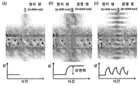
도 13은 본 발명의 실시예 1에 따라 제조된 구리 황화물 나노입자를 함유하는 큐벳을 적용한 PT OCR 센서이다.
도 14는 PT OCR를 이용한 PT 효과 검출의 원리를 나타낸 도면이다.
본 발명은 금속 황화물 나노입자의 크기 및 모양을 조절할 수 있는 금속 황화물 나노입자 및 이의 제조방법에 관한 것이다.
본 발명의 금속 황화물 나노입자는 판상형의 나노플레이트가 1 내지 100층으로 적층되어 형성되는 것으로서, 금속 싸이오사이안산 및 유기용매를 이용한 원-포트 방법(one-pot reaction)에 의해 수득된다.
이하, 본 발명을 상세하게 설명한다.
본 발명의 금속 황화물 나노입자를 제조하는 방법은 금속 싸이오사이안산 및 유기용매가 혼합된 혼합액을 진공하에서 교반하는 단계; 및 상기 교반된 혼합액을 기체 분위기 하에서 200 내지 400 ℃로 열처리 하는 단계;를 포함한다.
먼저, 전구체로 금속 싸이오사이안산 및 용매로 유기용매가 혼합된 혼합액을 80 내지 150 ℃, 바람직하게는 100 내지 120 ℃의 진공하에서 5 내지 20분 동안 교반한다.
상기 혼합액을 진공상태가 아닌 공기, 아르곤, 질소 또는 헬륨과 같은 기체하에서 교반하는 경우에는 이후 고온에서 열분해 시 금속 황화물 나노입자의 크기 및 모양을 조절할 수 없을 뿐만 아니라 균일하지 못한 나노입자를 형성할 수 있으므로 진공생태에서 교반하는 것이 바람직하다. 상기 크기는 나노입자의 입경 및 두께를 의미한다.
또한, 진공상태의 온도가 상기 하한치 미만인 경우에는 균일한 크기 및 모양의 금속 황화물 나노입자를 얻을 수 없으며, 상기 상한치 초과인 경우에는 부산물이 많이 생성되어 수율이 저하될 수 있다.
또한, 교반 시간이 상기 범위를 벗어난 경우에는 열분해 시 부산물이 다량 생성될 수 있다.
상기 금속 싸이오사이안산의 금속으로는 구리, 납, 코발트, 니켈, 아연, 티타늄, 카드뮴, 몰리브덴, 팔라듐, 로듐, 지르코늄, 바나듐, 하프늄 및 알루미늄으로 이루어진 군에서 선택된 1종 이상을 들 수 있으나, 이에 한정하는 것은 아니고 산업적으로 이용되는 모든 금속을 사용할 수 있다. 상기 금속 싸이오사이안산은 Mx(SCN)y로 표시되며, 열분해 시 MxSy로 표시되는 금속 황화물 나노입자가 제조된다. 이때, 상기 x 및 y는 각각 1 내지 10의 실수이다.
상기 유기용매로는 유기아민, 유기산 등의 유기용매의 종류가 특별히 한정되는 것은 아니지만; 바람직하게는 톨루엔, 디클로로벤젠, 도데칸, 옥타데씬, 스쿠알렌, 올레일아민, 옥타데실아민, 트리옥틸아민, 올레산, 스테아르산, 팔미트산, 엘라이드산, 박센산, 리놀렌산, 아라키돈산, 에루스산 및 베헨산 등으로 이루어진 군에서 선택된 1종 또는 2종 이상을 들 수 있으며; 더욱 바람직하게는 크기 및 모양의 용이한 제어 및 높은 균일성 면에서 올레일아민인 것이 바람직하다.
다음으로, 상기 교반된 혼합액을 기체 분위기 하에서 180 내지 400 ℃, 바람직하게는 200 내지 260 ℃로 10 내지 40분 동안 열처리하여 금속 싸이오사이안산을 열분해함으로써 금속 황화물 나노입자를 수득한다.
상기 혼합액 내 금속 싸이오사이안산의 농도는 1 내지 500 mM, 바람직하게는 1 내지 500 mM, 더욱 바람직하게는 1 내지 50 mM이다. 금속 싸이오사이안산의 농도가 상기 하한치 미만인 경우에는 금속 황화물 나노입자를 제조할 수 없으며, 상기 상한치 초과인 경우에는 판상형의 나노플레이트가 조립되는 것을 방해하여 두께를 제어할 수 없고 균일하지 못할 수 있다.
또한, 상기 열처리 온도가 상기 하한치 미만인 경우에는 금속 황화물 나노입자를 형성하는 시간이 오래 소요될 수 있으며, 상기 상한치 초과인 경우에는 금속 황화물 나노입자의 크기가 작아진다.
상기 금속 싸이오사이안산의 농도 및 열처리 온도는 상기 각 범위를 동시에 만족해야 나노입자의 크기 및 모양을 조절할 수 있을 뿐만 아니라 균일한 크기 및 모양의 나노입자를 다량으로 수득할 수 있는데, 상기 금속 싸이오사이안산의 농도 및 열분해 온도 중 하나라도 상기 범위를 만족하지 못한다면 상기 효과를 기대할 수 없다.
또한, 열처리 시간이 상기 하한치 미만인 경우에는 균일한 크기 및 모양의 금속 황화물 나노입자를 얻을 수 없으며, 상기 상한치 초과인 경우에는 부산물이 많이 생성되어 수율이 저하될 수 있다.
상기 기체는 고온의 열처리에서 나노입자의 모양 및 크기의 균일성을 유지하며 판상형 나노플레이트의 조립에 의한 크기 조절을 용이하게 하기 위하여 공기, 아르곤(Ar), 헬륨(He) 또는 질소(N2)기체를 사용하는 것이 바람직하며, 더욱 바람직하게는 아르곤(Ar) 기체를 이용하는 것이다.
또한, 본 발명은 금속 황화물 나노입자를 제공한다.
상기 금속 황화물 나노입자는 금속 싸이오사이안산을 유기용매 하에서 180 내지 400 ℃로 열분해하여 형성되는 것으로서, 판상형으로 형성되어 1 내지 100층으로 조립될 수 있다.
상기 금속 황화물 나노입자, 예컨대 판상형의 나노플레이트 하나의 평균입경은 20 내지 500 nm이며 두께는 2 내지 30 nm로서, 금속 싸이오사이안산의 농도 및 열처리 온도에 따라 나노입자의 입경크기 및 상기 나노플레이트의 적층 수를 조절하여 나노입자의 두께를 조절할 수 있다.
상기 적층된 금속 황화물 나노입자 사이의 거리(예컨대, 나노플레이트 간의 거리)는 0.5 내지 3.0 nm, 바람직하게는 1.1 내지 1.3 nm이다.
이하, 본 발명의 이해를 돕기 위하여 바람직한 실시예를 제시하나, 하기 실시예는 본 발명을 예시하는 것일 뿐 본 발명의 범주 및 기술사상 범위 내에서 다양한 변경 및 수정이 가능함은 당업자에게 있어서 명백한 것이며, 이러한 변형 및 수정이 첨부된 특허청구범위에 속하는 것도 당연한 것이다.
실시예 1. 구리 황화물 나노입자의 제조
고운 가루 형태의 전구체인 구리(I)싸이오사이안산(CuSCN) 화합물의 농도가 10 mM이 되도록 올레일아민(Oleylamine)과 함께 반응 용기에 넣은 후 100 ℃의 진공하에서 10분간 교반한 다음 아르곤(Ar) 가스로 채운다. 240 ℃로 예열되어 있는 오일욕에 상기 반응용기를 삽입하여 약 30분 동안 열처리한 후 상온으로 냉각하고 톨루엔 및 메탄올로 세척한 다음 원심분리하여 어두운 갈색의 구리 황화물 나노입자를 제조하였다.
실시예 2. 납 황화물 나노입자의 제조
상기 실시예 1과 동일하게 실시하되, 구리(I)싸이오사이안산(CuSCN) 화합물 대신 납(I)싸이오사이안산(PbSCN) 화합물을 사용하여 납 황화물 나노입자를 제조하였다.
실시예 3. 코발트 황화물 나노입자의 제조
상기 실시예 1과 동일하게 실시하되, 구리(I)싸이오사이안산(CuSCN) 화합물 대신 코발트(II)싸이오사이안산(Co(SCN)2) 화합물을 사용하여 코발트 황화물 나노입자를 제조하였다.
<시험예>
시험예 1. 구리 싸이오사이안산(CuSCN) 화합물의 농도에 따른 구리 황화물 나노입자의 TEM 이미지
구리(I)싸이오사이안산(CuSCN) 화합물의 농도를 1, 10, 20, 30, 40 및 50 mM로 하여 구리 황화물 나노입자를 제조하였으며, 상기 구리 황화물 나노입자는 Cu1.94S구조로 제조되었다.
도 1은 구리(I)싸이오사이안산(CuSCN) 화합물의 농도에 따라 제조된 평균입경이 다른 구리 황화물 나노입자를 TEM으로 촬영한 사진이다.
도 1에 도시된 바와 같이, 구리 황화물 나노입자의 평균입경은 구리(I)싸이오사이안산(CuSCN) 화합물의 농도가 증가할수록 증가하는 것을 확인하였다. 구체적으로, 구리(I)싸이오사이안산(CuSCN) 화합물의 농도가 1, 10, 20, 30, 40 및 50 mM인 경우에, 각각 72.2±2.8 nm, 86.1±2.9 nm, 99.4±3.8 nm, 106.7±3.3 nm, 116.6±7.2 nm 및 126.6±4.7 nm의 평균입경으로 구리 황화물 나노입자가 제조되었으며, 모든 농도 구간에서 균일한 육각 구리 황화물 나노입자를 형성하는 것을 확인하였다.
도 2a는 실시예 1에 따라 제조된 구리 황화물 나노입자를 낮은 배율에서 촬영한 TEM 사진이며; 도 2b는 실시예 1에 따라 제조된 구리 황화물 나노입자의 상면을 촬영한 TEM 사진이고; 도 2c는 실시예 1에 따라 제조된 구리 황화물 나노입자의 측면을 촬영한 TEM 사진이며; 도 2d-f는 실시예 1에 따라 제조된 구리 황화물 나노입자의 HRTEM 이미지 및 FFT pattern과 존 축(zone axis, 100)의 대응 이미지이고; 도 2g는 실시예 1에 따라 제조된 구리 황화물 나노입자의 XRD 패턴이며; 도 2h는 실시예 1에 따라 제조된 구리 황화물 나노입자의 STEM 이미지 및 니켈 그리드로 제조된 실시예 1의 구리 황화물 나노입자의 에너지 분산형 X-선 분광 분석 이미지이다. 이때, 원소 매핑 데이터는 66.34 % Cu 및 33.65 % S이다.
또한, 도 3은 실시예 1에 따라 제조되어 적층된 구리 황화물 나노입자의 측면을 촬영한 TEM 사진이며; 도 4는 JEMS(TEM 회절 및 이미지 시뮬레이션 소프트웨어) 시뮬레이션에 의한 결정 구조이다. 도 4에서 단위 셀에서 원자 결정 구조 및 FFT 패턴과 존 축[-1, 0, 0]이 보이며, 빨간 구형은 황 원자, 파랑 구형은 구리 원자로 표시하였다.
또한, 도 5는 Ni 그리드로 제조된 실시예 1의 구리 황화물 나노입자의 에너지 분산 X-선 스펙트럼이다.
도 2 내지 5에 도시된 바와 같이, 실시예 1에 따라 제조된 구리 황화물 나노입자는 평균입경 86.1 ± 2.9 nm, 두께 10.7 ± 1.3 nm로 매우 균일하게 형성된 것을 확인하였다(도 2a-c). 상기 평균입경은 나노입자(단일 나노플레이트)의 대각선 지점 간의 거리로 나타낸다. 표준 편차 값(σ)은 5% 미만이므로 이는 입경의 균일성을 나타낸다.
상기 실시예 1에 따라 제조된 구리 황화물 나노입자는 각각의 나노플레이트가 대면 적층 또는 엣지 공유로 조립되어 형성될 수 있으며, 상기 각 나노플레이트 사이의 거리는 약 1.28 nm이다(도 3).
또한, 실시예 1에 따라 제조된 구리 황화물 나노입자의 결정구조는 FFT 이미지에 나타낸 바와 같이 매우 복잡하다(도 2f). 상기 구조는 이전에 보고된 단사정계 시스템, 공간 그룹 P2
1
/n, a=26.897 Å, b=15.745 Å, c=13.565 Å, 및 β=90.13°과 일치한다.
구조적 복합성을 해결하기 위하여, FFT패턴은 TEM 회절 및 JEMS 소프트웨어로 수행한 컴퓨터 시뮬레이션을 조합하여 분석하였다(도 4).
실시예 1에 따라 제조된 구리 황화물 나노입자는 Cu1.94S로 제조되었으며, 상기 1.94의 비율은 XRD 패턴 및 TEM 회절 패턴 화상 시뮬레이션의 컴퓨터 시뮬레이션에 의해 확인되었다.
또한, 실시예 1에 따라 제조된 구리 황화물 나노입자의 높은 각도 환상 다크-필드 주사 TEM(HAADF-STEM) 이미지 및 에너지 분산 X-선(EDX) 스펙트럼은 단일 나노플레이트로 측정되었다(도 2h).
뿐만 아니라, 원소 맵핑 데이터는 육각 나노플레이트에서 Cu 및 S 원자 분포를 나타내며, 66.34% Cu 및 33.65% S 원자의 비는 Cu1.94S 상의 Cu/S 비와 매우 유사한 것을 확인하였다(도 5).
Cu1.94S 구조의 실시예 1 나노입자는 매우 안정하며, Cu2S 구조는 공기에 노출될 때 Cu1.94S 구조로 쉽게 변형되므로 안정하지 못하다. 단사, 육각형, 입방 및 사방정계를 포함하는 CuxS의 안정성은 △H
f 에 의해 비교된다.
디줄레아이트(djurleite) Cu1.94S는 △H
f = -0.40 eV로 단사정계 시스템이고, 낮은 휘동석(chalcocite) Cu2S 역시 △H
f = -0.41 eV로 단사정계 시스템이다. 이는 Cu1.94S가 구리가 풍부한 조건 및 Cu2S를 쉽게 형성할 수 있는 구리 공석에서 Cu2S보다 안정적임을 의미한다.
시험예 2. 구리 황화물 나노입자의 크기 및 모양 조절
도 6의 검정 막대 높이는 실시예 1에 따라 제조된 나노입자의 두께이며, 검정 막대와 파랑 막대가 결합된 높이는 상기 나노입자의 입경이다. 열처리 온도에 따른 입경/두께 비율 변화는 빨강 점으로 표시되며, 이는 우측에 도시된 스케일에 따라 읽는다.
도 7은 240 ℃에서 반응 시간 a) 5 분, b) 10 분, c) 20 분, d) 30 분에 따른 실시예 1의 나노입자 평균입경의 변화를 나타낸 그래프이다.
도 6 및 7에 도시된 바와 같이, 실시예 1 나노입자의 평균입경은 전구체 농도 및 열처리 온도 변화에 의해 조절될 수 있다. 상기 나노입자의 성장은 20분의 반응시간(도 7) 후 매우 느려지고, 나노입자 모양은 반응온도 240 ℃에서 1 시간동안 가열 시에도 손상되지 않는 것을 확인하였다.
실시예 1 나노입자의 평균입경은 증가된 전구체 농도로 증가되고 높은 반응온도로 감소된다. 핵이 높은 온도에서 촉진되고, 전체적으로 나노입자의 평균입경의 크기 감소를 초래하였다.
실시예 1 나노입자의 입경/두께 비율은 증가된 열처리 온도에 의해 감소되는데, 이는 낮은 반응온도에서 폭 방향을 따라 나노입자의 길이 방향의 존재를 나타낸다.
따라서, 전구체 농도 및 열처리 온도에 따라 나노입자의 크기(평균입경 및 두께) 및 모양을 제어할 수 있다.
시험예 3. 밴드갭 측정
도 8a는 실시예 1에 따라 제조된 구리 황화물 나노입자의 흡수 그래프이고, 삽입도는 광 발광 흡수 그래프이다. PL 스펙트럼은 350 nm 여기에서 촬영하였다.
또한, 도 8b는 실시예 1에 따라 제조된 구리 황화물 나노입자의 간접 밴드갭의 평가에 대한 (αhυ)1/2vs. h의 플롯, 직접 밴드갭의 평가에 대한 (αhυ)2vs. h의 플롯이다.
도 8에 도시된 바와 같이, 실시예 1에 따라 제조된 구리 황화물 나노입자의 광 흡수 스펙트럼은 UV에서 IR까지의 넓은 범위의 흡광도를 보여주며, 실시예 1 나노입자의 광범위한 흡수는 태양전지 흡수제로 적합하다.
도 8a의 삽입도에 도시된 바와 같이, 실시예 1 나노입자의 광 발광 스펙트럼은 이전에 보고된 것과 유사한 직접 밴드갭 전환에서 유래된 405, 427 및 450 nm에서 발광피크를 보인다. 보고된 황화구리 나노입자는 UV 영역에서 직접 밴드갭 및 NIR 영역에서 간접 밴드갭 때문에 두 개의 흡수피크를 보인다.
하기 [수학식 1]과 같이, 광 밴드갭 E
g 및 흡수단 부근의 대응 흡수 계수 α의 관계를 나타낸다.
수학식 1 
상기 C는 상수이고, hυ는 광 에너지이며, k 값은 직접 밴드에 대한 0.5 및 간접 밴드에 대한 2이다.
그러므로 광 밴드갭은 플롯, 즉 Tauc 플롯의 피팅라인을 추정에 의해 산정할 수 있다.
또한, 도 8b에 도시된 바와 같이, 제조된 실시예 1 나노입자의 직접 및 간접 광 밴드갭은 각각 1.22 eV 및 2.19 eV로 산정되었다.
시험예 4. 광열 효과 분석
도 9는 실시예 1에 따라 제조된 구리 황화물 나노입자의 PT응답으로서, 구리 황화물 나노입자 농도에 따라 측정된 위상 신호그래프이다. PT 여기 광원 소스의 세기는 6 W/cm2이다(삽입도). 에러 막대의 측정에 기초하여 표준오차를 나타낸다.
도 9에 도시된 바와 같이, 6 W/cm2 PT 광 조사로 60초 동안 측정된 위상 신호로서, PT 여기 광원은 1 Hz 변화로 변화된다. 실시예 1 나노입자 용액은 PT 여기 하에서 매우 두드러진 위상이 측정된 반면, 나노입자가 없는 용액은 ~1064 nm에서 톨루엔의 극한 흡수 때문에 작은 위상 변화가 나타난다.
또한, 상이한 나노입자 농도에서 PT 응답이 측정되는데, 이는 측정된 PT 반응이 실시예 1 나노입자 용액의 농도에 따라 선형 변화됨을 알 수 있다.
이러한 결과는 세포 리시스(lysis) 및 박테리아와 같은 병원균을 비활성화시키는 강력한 광열 치료제로 나노입자의 가능성을 시사한다.
시험예 5. 광열 치료제로서의 가능성
용기에 실시예 1에 따라 제조된 구리 황화물 나노입자와 H3N2 바이러스를 함께 투입한 후 광열(photothermal, PT, 여기 광원 소스의 세기는 6 W/cm2임)을 조사한 후 세포 리시스(lysis) 활성을 측정하였다.
구체적으로, 구리 황화물 나노입자와 H3N2 바이러스를 함께 투입한 후 광열을 조사하면 빛을 받은 나노입자가 빛을 열로 변환시키면서 바이러스를 분해시켜 상기 바이러스 내부의 유전정보를 방출한다.
하기 [표 1]에는 실험조건을 나타내었고, 하기 [표 2]에는 각 샘플에 따른 세포 리시스(lysis) 활성화, 혈구응집소 농도(hemagglutinin titer) 및 전염성을 측정하였다. 대조군으로는 나노입자를 사용하지 않고 광열만 조사하였다.
표 1
| 구분 | 구리 황화물의 농도(mg/ml) | 광열 조사 시간(초) |
| 샘플 1 | 0.015 | 30 |
| 샘플 2 | 0.01 | 30 |
| 샘플 3 | 0.005 | 30 |
| 샘플 4 | 0.002 | 30 |
| 샘플 5 | 0.015 | 180 |
| 샘플 6 | 0.01 | 180 |
| 샘플 7 | 0.005 | 180 |
| 샘플 8 | 0.002 | 180 |
| 샘플 9 | 0.015 | 1200 |
표 2
| 구분 | 세포 리시스 | 혈구응집소 농도 | 전염성 |
| 대조군 | 음성 | - | 높음 |
| 샘플 1 | 양성 | <2 | 낮음 |
| 샘플 2 | 양성 | <2 | 낮음 |
| 샘플 3 | 양성 | 2 | 낮음 |
| 샘플 4 | 음성 | 128 | 낮음 |
| 샘플 5 | 양성 | <2 | 낮음 |
| 샘플 6 | 양성 | <2 | 낮음 |
| 샘플 7 | 양성 | 4 | 낮음 |
| 샘플 8 | 음성 | 128 | 낮음 |
| 샘플 9 | 양성 | <2 | 낮음 |
위 표 2에 나타낸 바와 같이, 샘플 1 내지 9는 대조군과 달리, 전염성이 모두 낮으며, 특히 샘플 1, 2, 3, 5, 6, 7, 9는 세포 리시스에 대하여 양성이며 혈구응집소 농도가 다른 군에 비하여 낮은 것을 확인하였습니다.
이러한 결과는 샘플 1, 2, 3, 5, 6, 7, 9가 세포 리시스(lysis)와 같은 병원균을 비활성화시키는 강력한 광열 치료제로 나노입자의 가능성을 시사한다.
시험예 6. 납 황화물 나노입자 및 코발트 황화물 나노입자에 대한 TEM 이미지 및 X-선 회전 패턴 분석
도 10은 실시예 2에 따라 제조된 납 황화물 나노입자를 TEM으로 촬영한 사진이며; 도 11은 실시예 2에 따라 제조된 납 황화물 나노입자를 X-선 회전 패턴이다.
도 12는 실시예 3에 따라 제조된 코발트 황화물 나노입자를 X-선 회전 패턴이다.
도 10 및 11에 도시된 바와 같이, 실시예 2의 납 황화물 나노입자가 단일 또는 적층되어 형성되는 것을 확인하였다. 또한, X-선 회절 패턴으로 납 황화물(PbS)이 생성되었음을 확인하였다.
또한, 도 12에 도시된 바와 같이, X-선 회절 패턴으로 코발트 황화물(CoS)이 생성되었음을 확인하였다.
유기용매 하에서 단일 전구체 금속 싸이오사이안산의 열분해가 수행되어 매우 균일한 크기 및 모양으로 금속 황화물 나노입자가 다량 수득된다. 상기 금속 황화물 나노입자의 크기(입경 및 두께)는 열처리 온도 및 전구체 농도의 변화에 의해 제어될 수 있다.
또한, 금속 황화물 나노입자는 세포 리시스(lysis) 및 박테리아와 같은 병원균을 비활성화시키도록 광열 치료에 적용할 수 있다.
-장치-
투과 전자 현미경(TEM) 및 고해상도 TEM(HRTEM)은 각각 200 kV에서 작동되는 TECNAI G2 20 STwin 및 300 kV에서 작동되는 TECNAI G2 F30에서 수행되었다.
원소 매핑 및 에너지 분산형 X-선 스펙트럼(EDX)은 Chemi-STEM 기술 및 JEOL ARM200F Cs STEM과 FEI Titan Cubed 60-300으로 얻었다.
또한, X-선 회절(XRD) 패턴은 40 kV 및 40 mA에서 흑연-모노크롬산화된 Cu-Kα 반사선을 이용한 Rigaku Ultima III 회절 시스템으로 수집되었다.
-광학 위상변화 조사-
도 13은 840 nm 초발광 레이저 다이오드를 프로브 광원을 채용하고, 실시예 1 나노입자를 함유하는 큐벳을 적용한 PT OCR 센서이다.
도 14는 PT OCR를 이용한 PT 효과 검출의 원리를 나타낸 도면이다. (a) 위상 신호는 여기 광 없는 주목할 변화가 없다. (b) PT 레이저 조명은 SDOCR 위상 신호의 변화로 이어지는 PT 광 조명 용적 내부의 온도 변화를 유도한다. (c) 온도 변화 및 기계적 진동 등의 배경 노이즈는 PT 광 강도 변화를 도입함으로써 배제할 수 있다.
최근에는, 근적외선 영역에서 종양치사 효과에 유용할 수 있는 황화구리의 광열효과가 보고되었다. 미래 테라그노스틱(theragnostic) 적용을 위해 생분해 광열 에이전트를 개발하는 것이 중요하며, 광열에 적용하기 위해 사용되는 금 나노입자는 생분해되지 않는 문제가 있다.
본 발명의 금속 황화물 나노입자의 광열 반응을 이해하기 위하여, 수성 나노입자 용액으로 채운 석영 큐벳에서 반사된 840 nm 프로브 광의 광학 위상 변화(△Φ)를 조사하였다(도 13, 14).
내부 쳄버의 상부 및 하부로부터 반사에서 간섭 사이의 위상을 측정하였으며, 1064 nm 광열(PT) 여기광의 조사에 의해 나노입자는 열을 발생하는 PT 광 에너지를 흡수한다.
상기 열 변화는 챔버의 상부 및 하부 표면 사이의 상이한 광학 위상차 변화를 이끈다.
하기에서는 광열 빛 간섭 반사(PT OCR)의 작동에 대하여 설명한다.
기준 및 측정 광의 간섭이 측정되는 낮은 응집 스펙트럼의 간섭계에 기초하고, 표본의 경로-길이 해결된 복합-값 정보에서 변환된다.
PT OCR 설정(도 13)에서, 초발광 레이저 다이오드로부터 840 nm 프로브 광은 수성 실시예 1의 나노입자로 채워진 챔버를 조사한다. 이때 광원의 3-dB 대역폭 스펙트럼은 ~50 nm이다.
챔버의 표면에서 반사는 분광계(USB 4000, Ocean Optics, Inc., Canada)로 지시되었으며, 간섭과 관련된 스펙트럼은 다음 [수학식 2]와 같이 쓸 수 있다;
수학식 2 
여기서, k 는 파수이고, S(k)는 광원의 전력 스펙트럼 밀도이며, R
r 및 R
s (z
n )은 두 표면 사이의 광학 경로-길이 차이로 각각 빔 경로를 따라 기준면 및 n번째 측정면의 반사율이다.
내부 챔버의 상부면을 기준으로 사용하였으며, 간섭 스펙트럼의 역 푸리에 변형과 2k 산출 경로-길이 분해된 복합-값 정보, F(z)을 생성한다.
상기 내부 챔버의 상부 및 하부면으로부터의 반사 사이의 간섭에 관련된 간섭 신호를 찾으며, 시간 함수로서 그 위상을 감시한다([수학식 3]).
z n , Φ(z n ),경로길이에서 간섭 신호의 위상은 평가될 수 있다.
수학식 3 
1064 nm PT 레이저 조사에 앞서, 어떠한 상 변화도 측정되지 않았다(도 15).
PT 레이저 조사할 때, 실시예 1의 나노입자는 1064 nm 광 에너지를 흡수하며 PT 효과 때문에 온도 상승을 이끈다.
온도의 함수로서 굴절율(n) 때문에, 챔버 내부의 온도 변화는 간섭 신호의 위상 변화를 관찰함으로써 모니터링될 수 있다(도 14).
상기 측정된 상 변화(△Φ)는 굴절율 변화(△n)와 관련이 있다([수학식 4]):
수학식 4 
여기서, k
0 및 λ0은 SD-OCR 광의 중심 파수 및 파장이고; L은 광이 통과된 물리적 거리, 즉 내부 챔버의 높이이다.
PT 효과에 의한 위상 변화의 측정은 PT 레이저의 연속 또는 강도 조절 조사로 수행될 수 있다. 그러나, 실제로 이러한 온도 경향 및 진동과 같은 외부 교란은 안정적인 위상 측정에 영향을 미칠 수 있다.
그러므로, 향상된 신호 대 노이즈(SNR)와 같은 위상 변화의 고감도 측정이 가능하게 강도-변조 방식을 채용하였다(도 14).
PT 빔의 변화 주파수 부근의 신호 측정에 의해, 측정은 최소화되고 다른 주파수 범위에서 노이즈 성분의 효과로서 정확하게 수행될 수 있다.
강도- 변화는 PT 빔 경로에서 광 초퍼를 사용하여 달성하였다(초퍼 휠로 광학 초퍼 시스템; MC1F2, Thorlabs, USA).
취득된 위상 신호는 프리에 변환되고, PT OCR 신호를 나타내는 변화 주파수를 중심으로 그 크기가 조사되었다.
본 발명의 금속 황화물 나노입자는 세포 리시스(lysis) 및 박테리아와 같은 병원균을 비활성화시키는 강력한 광열 치료제로 이용될 수 있다.
Claims (14)
- 금속 싸이오사이안산을 유기용매 하에서 열분해하여 형성되는 것을 특징으로 하는 금속 황화물 나노입자.
- 제1항에 있어서, 상기 금속 황화물 나노입자는 판상형으로서 1 내지 100 층으로 적층되는 것을 특징으로 하는 금속 황화물 나노입자.
- 제1항에 있어서, 상기 금속 싸이오사이안산과 유기용매가 혼합된 용액 내 금속 싸이오사이안산의 농도는 1 내지 500 mM인 것을 특징으로 하는 금속 황화물 나노입자.
- 제1항에 있어서, 상기 열분해 온도는 100 내지 400 ℃인 것을 특징으로 하는 금속 황화물 나노입자.
- 제1항에 있어서, 상기 금속 싸이오사이안산의 금속은 구리, 납, 코발트, 니켈, 아연, 티타늄, 카드뮴, 몰리브덴, 팔라듐, 로듐, 지르코늄, 바나듐, 하프늄 및 알루미늄으로 이루어진 군에서 선택된 1종 이상인 것을 특징으로 하는 금속 황화물 나노입자.
- 제1항에 있어서, 상기 유기용매는 톨루엔, 디클로로벤젠, 도데케인, 옥타데씬, 올레일아민, 옥타데실아민, 트리옥틸아민, 올레산, 스테아르산, 팔미트산, 엘라이드산, 박센산, 리놀렌산, 아라키돈산, 에루스산 및 베헨산으로 이루어진 군에서 선택된 1종 또는 2종 이상인 것을 특징으로 하는 금속 황화물 나노입자.
- 제1항에 있어서, 상기 금속 황화물 나노입자의 평균입경은 20 내지 500 nm이며, 두께는 2 내지 30 nm인 것을 특징으로 하는 금속 황화물 나노입자.
- 제2항에 있어서, 상기 적층된 금속 황화물 나노입자 사이의 거리는 0.5 내지 3.0 nm인 것을 특징으로 하는 금속 황화물 나노입자.
- 금속 싸이오사이안산 및 유기용매가 혼합된 혼합액을 진공하에서 교반하는 단계; 및상기 교반된 혼합액을 기체 분위기 하에서 100 내지 400 ℃로 열처리 하는 단계;를 포함하는 것을 특징으로 하는 금속 황화물 나노입자의 제조방법.
- 제9항에 있어서, 상기 혼합액은 80 내지 150 ℃의 진공하에서 교반되는 것을 특징으로 하는 금속 황화물 나노입자의 제조방법.
- 제9항에 있어서, 상기 혼합액 내 금속 싸이오사이안산의 농도는 1 내지 500 mM인 것을 특징으로 하는 금속 황화물 나노입자의 제조방법.
- 제9항에 있어서, 상기 기체는 공기, 아르곤(Ar), 헬륨(He) 또는 질소(N2)기체인 것을 특징으로 하는 금속 황화물 나노입자의 제조방법.
- 제9항에 있어서, 상기 금속 싸이오사이안산의 금속은 구리, 납, 코발트, 니켈, 아연, 티타늄, 카드뮴, 몰리브덴, 팔라듐, 로듐, 지르코늄, 바나듐, 하프늄 및 알루미늄으로 이루어진 군에서 선택된 1종 이상인 것을 특징으로 하는 금속 황화물 나노입자의 제조방법.
- 제9항에 있어서, 상기 유기용매는 톨루엔, 디클로로벤젠, 도데케인, 옥타데씬, 올레일아민, 옥타데실아민, 트리옥틸아민, 올레산, 스테아르산, 팔미트산, 엘라이드산, 박센산, 리놀렌산, 아라키돈산, 에루스산 및 베헨산으로 이루어진 군에서 선택된 1종 또는 2종 이상인 것을 특징으로 하는 금속 황화물 나노입자의 제조방법.
Applications Claiming Priority (2)
| Application Number | Priority Date | Filing Date | Title |
|---|---|---|---|
| KR10-2015-0062695 | 2015-05-04 | ||
| KR1020150062695A KR101786897B1 (ko) | 2015-05-04 | 2015-05-04 | 금속 황화물 나노입자 및 이의 제조방법 |
Publications (1)
| Publication Number | Publication Date |
|---|---|
| WO2016195244A1 true WO2016195244A1 (ko) | 2016-12-08 |
Family
ID=57441603
Family Applications (1)
| Application Number | Title | Priority Date | Filing Date |
|---|---|---|---|
| PCT/KR2016/004313 Ceased WO2016195244A1 (ko) | 2015-05-04 | 2016-05-02 | 금속 황화물 나노입자 및 이의 제조방법 |
Country Status (2)
| Country | Link |
|---|---|
| KR (1) | KR101786897B1 (ko) |
| WO (1) | WO2016195244A1 (ko) |
Cited By (2)
| Publication number | Priority date | Publication date | Assignee | Title |
|---|---|---|---|---|
| CN119118185A (zh) * | 2024-11-13 | 2024-12-13 | 国科大杭州高等研究院 | 一种等离子共振吸收连续可调的Cu2-xS纳米颗粒制备方法 |
| CN119332283A (zh) * | 2024-09-02 | 2025-01-21 | 宁夏大学 | 一种Cu2S-CdS异质结纳米片的制备方法 |
Families Citing this family (4)
| Publication number | Priority date | Publication date | Assignee | Title |
|---|---|---|---|---|
| KR102443380B1 (ko) | 2020-11-24 | 2022-09-19 | 한국과학기술연구원 | 전기화학적 질소환원을 위한 다중공 금속황화물 나노입자의 제조방법 및 이에 따라 제조된 다중공 금속황화물 나노입자 |
| US20240263324A1 (en) * | 2021-05-31 | 2024-08-08 | Korea University Research And Business Foundation | Iridium/ruthenium-based anode catalyst for water electrolysis, method for preparing same, and water electrolysis device using same |
| KR102420119B1 (ko) * | 2021-11-19 | 2022-07-13 | 대한기술연구원 주식회사 | 고습윤 환경에 노출된 수처리 콘크리트 구조물의 타일 시공방법 |
| KR102889327B1 (ko) | 2022-11-29 | 2025-11-24 | 나노씨엠에스(주) | 황화구리 나노 입자의 제조방법 및 이에 의하여 제조된 황화구리 나노 입자를 포함하는 근적외선 흡수제 |
Family Cites Families (3)
| Publication number | Priority date | Publication date | Assignee | Title |
|---|---|---|---|---|
| US4447335A (en) | 1981-03-31 | 1984-05-08 | Argus Chemical Corporation | Process for the preparation of thin films of cadmium sulfide and precursor solutions of cadmium ammonia thiocyanate complex useful therein |
| KR100296981B1 (ko) | 1998-09-30 | 2001-10-27 | 오길록 | 금속황화물박막제조방법및전계발광소자제조방법 |
| KR100407194B1 (ko) | 2001-02-14 | 2003-11-28 | 가야에이엠에이 주식회사 | 금속 황화물의 제조방법 |
-
2015
- 2015-05-04 KR KR1020150062695A patent/KR101786897B1/ko active Active
-
2016
- 2016-05-02 WO PCT/KR2016/004313 patent/WO2016195244A1/ko not_active Ceased
Non-Patent Citations (7)
| Title |
|---|
| CHOI, SANG - HYUN ET AL.: "Simple and Generalized Synthesis of Semiconducting Metal Sulfide Nanocrystals", ADVANCED FUNCTIONAL MATERIALS, vol. 19, no. 10, 2009, pages 1645 - 1649, XP055332392 * |
| HA, DON - HYUNG ET AL.: "Solid-solid Phase Transformations Induced through Cation Exchange and Strain in 2D Heterostructured Copper Sulfide Nanocrystals", NANO LETTERS, vol. 14, no. 12, 2014, pages 7090 - 7099, XP055332384 * |
| KOH, WEON - KYU ET AL.: "Thiocyanate-capped PbS Nanocubes: Ambipolar Transport enables Quantum Dot based Circuits on a Flexible Substrate", NANO LETTERS, vol. 11, no. 11, 2011, pages 4764 - 4767, XP055332390 * |
| LI, WENHUA ET AL.: "Morphology Evolution of Cu2-xS Nanoparticles: from Spheres to Dodecahedrons", CHEMICAL COMUNICATIONS, vol. 47, no. 37, 2011, pages 10332 - 10334 * |
| REGULACIO, MICHELLE D. ET AL.: "One-pot Synthesis of Cul.94S-CdS and Cul .94S-ZnxCd1-xS Nanodisk Heterostructures", JOURNAL OF THE AMERICAN CHEMICAL SOCIETY, vol. 133, no. 7, 2011, pages 2052 - 2055, XP055332383 * |
| YOON, DONG HWAN ET AL.: "Synthesis of Copper Sulfide Hexagonal Nanoplate and their Photothermal Effect", THE 115TH GENERAL MEETING OF THE KOREAN CHEMICAL SOCIETY, 15 April 2015 (2015-04-15) * |
| YOON, DONGHWAN ET AL.: "Scalable Synthesis of Djurleite Copper Sulphide (Cul.94S) Hexagonal Nanoplates from a Single Precursor Copper Hiocyanate and their Photothermal Properties", CRYSTENGCOMM, vol. 17, no. 25, 14 May 2015 (2015-05-14), pages 4627 - 4631 * |
Cited By (2)
| Publication number | Priority date | Publication date | Assignee | Title |
|---|---|---|---|---|
| CN119332283A (zh) * | 2024-09-02 | 2025-01-21 | 宁夏大学 | 一种Cu2S-CdS异质结纳米片的制备方法 |
| CN119118185A (zh) * | 2024-11-13 | 2024-12-13 | 国科大杭州高等研究院 | 一种等离子共振吸收连续可调的Cu2-xS纳米颗粒制备方法 |
Also Published As
| Publication number | Publication date |
|---|---|
| KR20160130649A (ko) | 2016-11-14 |
| KR101786897B1 (ko) | 2017-10-18 |
Similar Documents
| Publication | Publication Date | Title |
|---|---|---|
| WO2016195244A1 (ko) | 금속 황화물 나노입자 및 이의 제조방법 | |
| Rayerfrancis et al. | Effect of pH on the morphology of ZnO nanostructures and its influence on structural and optical properties | |
| Subashini et al. | Acetone sensing behaviour of optical fiber clad-modified with γ-CuBr nanocrystals | |
| Xu et al. | Facile synthesis and phase transition of V 2 O 3 nanobelts | |
| Karuppasamy et al. | Crystal growth and physico-chemical characterization of semi-organic [C4H12N2] ZnCl4· H2O single crystal for laser applications | |
| Wang et al. | UV photodetector properties of CsPbCl3 grown by Vertical Bridgman method | |
| Bayansal et al. | Mechanical and structural properties of Li-doped CuO thin films deposited by the successive ionic layer adsorption and reaction method | |
| WO2018143611A1 (ko) | 대면적 금속 칼코겐 박막의 제조방법 및 이에 의해 제조된 금속 칼코겐 박막을 포함하는 전자소자의 제조방법 | |
| Aguilar et al. | Non-destructive optical second harmonic generation imaging of 3D printed aluminum nitride ceramics | |
| Santhaveesuk et al. | Ethanol sensing properties of Zn2TiO4 particles | |
| Singh et al. | Ethanol sensing using MoS2/TiO2 composite prepared via hydrothermal method | |
| WO2016043396A1 (ko) | 질소 도핑된 그래핀의 제조방법 및 이로부터 제조된 질소 도핑된 그래핀 | |
| Parida et al. | Structural, thermal, and optical characterization of ZrC-ZnO composites for UV/blue light emission | |
| Gotoh et al. | Photothermal bending spectroscopy and photothermal deflection spectroscopy of C60 thin films | |
| Wang et al. | Bismuth Chalcohalide Bi13S18Br2 for Fast and Sensitive Near‐Infrared Photodetection | |
| Karthieka et al. | Low-dose X-ray sensing nature of nanostructured Zn (Cu) O thick films | |
| Zhang et al. | Structural features, low-temperature luminescence properties of Li-doped SnO2 nanobelts and their transitional temperature | |
| Wang et al. | Large-scale synthesis of β-AgI nanocrystals | |
| Liu et al. | CVD approach to a single gallium oxide nanowire for solar-blind UV detector | |
| Dhas et al. | Spectral, optical, thermal and mechanical studies on l-Histidine oxalate crystals | |
| Kedarnath et al. | Synthesis and characterization of metal selenide (ZnSe, CdSe, HgSe) nanoparticles | |
| Kakherskyi et al. | Influence of Low-Temperature Annealing on the Structure and Chemical Composition of Cu2ZnSnS4 Films Deposed on Flexible Polyimide Substrates | |
| Lazoryk et al. | Peculiarities of photoluminescence in gas ambient of doped ZnO nanopowders | |
| Vishwakarma et al. | Enhanced Short-Wave Infrared Detection Using Colloidal-Synthesized AgFeS2 Nanocrystals | |
| Swati et al. | Size-selective and facile synthesis of zno/zns core–shell nanostructure and its characterization |
Legal Events
| Date | Code | Title | Description |
|---|---|---|---|
| 121 | Ep: the epo has been informed by wipo that ep was designated in this application |
Ref document number: 16803599 Country of ref document: EP Kind code of ref document: A1 |
|
| NENP | Non-entry into the national phase |
Ref country code: DE |
|
| 122 | Ep: pct application non-entry in european phase |
Ref document number: 16803599 Country of ref document: EP Kind code of ref document: A1 |