WO2016190375A1 - ホウ素添加酸化亜鉛薄膜からなる低摩擦コーティングおよびマイクロマシン - Google Patents
ホウ素添加酸化亜鉛薄膜からなる低摩擦コーティングおよびマイクロマシン Download PDFInfo
- Publication number
- WO2016190375A1 WO2016190375A1 PCT/JP2016/065521 JP2016065521W WO2016190375A1 WO 2016190375 A1 WO2016190375 A1 WO 2016190375A1 JP 2016065521 W JP2016065521 W JP 2016065521W WO 2016190375 A1 WO2016190375 A1 WO 2016190375A1
- Authority
- WO
- WIPO (PCT)
- Prior art keywords
- zinc oxide
- thin film
- oxide thin
- friction
- pfm
- Prior art date
- Legal status (The legal status is an assumption and is not a legal conclusion. Google has not performed a legal analysis and makes no representation as to the accuracy of the status listed.)
- Ceased
Links
Images




Classifications
-
- B—PERFORMING OPERATIONS; TRANSPORTING
- B81—MICROSTRUCTURAL TECHNOLOGY
- B81B—MICROSTRUCTURAL DEVICES OR SYSTEMS, e.g. MICROMECHANICAL DEVICES
- B81B3/00—Devices comprising flexible or deformable elements, e.g. comprising elastic tongues or membranes
- B81B3/0002—Arrangements for avoiding sticking of the flexible or moving parts
- B81B3/0005—Anti-stiction coatings
-
- B—PERFORMING OPERATIONS; TRANSPORTING
- B81—MICROSTRUCTURAL TECHNOLOGY
- B81B—MICROSTRUCTURAL DEVICES OR SYSTEMS, e.g. MICROMECHANICAL DEVICES
- B81B3/00—Devices comprising flexible or deformable elements, e.g. comprising elastic tongues or membranes
- B81B3/0064—Constitution or structural means for improving or controlling the physical properties of a device
- B81B3/0067—Mechanical properties
- B81B3/0078—Constitution or structural means for improving mechanical properties not provided for in B81B3/007 - B81B3/0075
-
- B—PERFORMING OPERATIONS; TRANSPORTING
- B81—MICROSTRUCTURAL TECHNOLOGY
- B81B—MICROSTRUCTURAL DEVICES OR SYSTEMS, e.g. MICROMECHANICAL DEVICES
- B81B7/00—Microstructural systems ; Auxiliary parts of microstructural devices or systems
- B81B7/02—Microstructural systems ; Auxiliary parts of microstructural devices or systems containing distinct electrical or optical devices of particular relevance for their function, e.g. microelectro-mechanical systems [MEMS]
-
- C—CHEMISTRY; METALLURGY
- C10—PETROLEUM, GAS OR COKE INDUSTRIES; TECHNICAL GASES CONTAINING CARBON MONOXIDE; FUELS; LUBRICANTS; PEAT
- C10M—LUBRICATING COMPOSITIONS; USE OF CHEMICAL SUBSTANCES EITHER ALONE OR AS LUBRICATING INGREDIENTS IN A LUBRICATING COMPOSITION
- C10M103/00—Lubricating compositions characterised by the base-material being an inorganic material
- C10M103/06—Metal compounds
-
- C—CHEMISTRY; METALLURGY
- C23—COATING METALLIC MATERIAL; COATING MATERIAL WITH METALLIC MATERIAL; CHEMICAL SURFACE TREATMENT; DIFFUSION TREATMENT OF METALLIC MATERIAL; COATING BY VACUUM EVAPORATION, BY SPUTTERING, BY ION IMPLANTATION OR BY CHEMICAL VAPOUR DEPOSITION, IN GENERAL; INHIBITING CORROSION OF METALLIC MATERIAL OR INCRUSTATION IN GENERAL
- C23C—COATING METALLIC MATERIAL; COATING MATERIAL WITH METALLIC MATERIAL; SURFACE TREATMENT OF METALLIC MATERIAL BY DIFFUSION INTO THE SURFACE, BY CHEMICAL CONVERSION OR SUBSTITUTION; COATING BY VACUUM EVAPORATION, BY SPUTTERING, BY ION IMPLANTATION OR BY CHEMICAL VAPOUR DEPOSITION, IN GENERAL
- C23C14/00—Coating by vacuum evaporation, by sputtering or by ion implantation of the coating forming material
- C23C14/06—Coating by vacuum evaporation, by sputtering or by ion implantation of the coating forming material characterised by the coating material
- C23C14/08—Oxides
-
- C—CHEMISTRY; METALLURGY
- C23—COATING METALLIC MATERIAL; COATING MATERIAL WITH METALLIC MATERIAL; CHEMICAL SURFACE TREATMENT; DIFFUSION TREATMENT OF METALLIC MATERIAL; COATING BY VACUUM EVAPORATION, BY SPUTTERING, BY ION IMPLANTATION OR BY CHEMICAL VAPOUR DEPOSITION, IN GENERAL; INHIBITING CORROSION OF METALLIC MATERIAL OR INCRUSTATION IN GENERAL
- C23C—COATING METALLIC MATERIAL; COATING MATERIAL WITH METALLIC MATERIAL; SURFACE TREATMENT OF METALLIC MATERIAL BY DIFFUSION INTO THE SURFACE, BY CHEMICAL CONVERSION OR SUBSTITUTION; COATING BY VACUUM EVAPORATION, BY SPUTTERING, BY ION IMPLANTATION OR BY CHEMICAL VAPOUR DEPOSITION, IN GENERAL
- C23C14/00—Coating by vacuum evaporation, by sputtering or by ion implantation of the coating forming material
- C23C14/06—Coating by vacuum evaporation, by sputtering or by ion implantation of the coating forming material characterised by the coating material
- C23C14/08—Oxides
- C23C14/086—Oxides of zinc, germanium, cadmium, indium, tin, thallium or bismuth
-
- C—CHEMISTRY; METALLURGY
- C23—COATING METALLIC MATERIAL; COATING MATERIAL WITH METALLIC MATERIAL; CHEMICAL SURFACE TREATMENT; DIFFUSION TREATMENT OF METALLIC MATERIAL; COATING BY VACUUM EVAPORATION, BY SPUTTERING, BY ION IMPLANTATION OR BY CHEMICAL VAPOUR DEPOSITION, IN GENERAL; INHIBITING CORROSION OF METALLIC MATERIAL OR INCRUSTATION IN GENERAL
- C23C—COATING METALLIC MATERIAL; COATING MATERIAL WITH METALLIC MATERIAL; SURFACE TREATMENT OF METALLIC MATERIAL BY DIFFUSION INTO THE SURFACE, BY CHEMICAL CONVERSION OR SUBSTITUTION; COATING BY VACUUM EVAPORATION, BY SPUTTERING, BY ION IMPLANTATION OR BY CHEMICAL VAPOUR DEPOSITION, IN GENERAL
- C23C14/00—Coating by vacuum evaporation, by sputtering or by ion implantation of the coating forming material
- C23C14/22—Coating by vacuum evaporation, by sputtering or by ion implantation of the coating forming material characterised by the process of coating
- C23C14/34—Sputtering
- C23C14/35—Sputtering by application of a magnetic field, e.g. magnetron sputtering
-
- B—PERFORMING OPERATIONS; TRANSPORTING
- B81—MICROSTRUCTURAL TECHNOLOGY
- B81B—MICROSTRUCTURAL DEVICES OR SYSTEMS, e.g. MICROMECHANICAL DEVICES
- B81B2201/00—Specific applications of microelectromechanical systems
- B81B2201/03—Microengines and actuators
- B81B2201/035—Microgears
-
- B—PERFORMING OPERATIONS; TRANSPORTING
- B81—MICROSTRUCTURAL TECHNOLOGY
- B81C—PROCESSES OR APPARATUS SPECIALLY ADAPTED FOR THE MANUFACTURE OR TREATMENT OF MICROSTRUCTURAL DEVICES OR SYSTEMS
- B81C2201/00—Manufacture or treatment of microstructural devices or systems
- B81C2201/01—Manufacture or treatment of microstructural devices or systems in or on a substrate
- B81C2201/0101—Shaping material; Structuring the bulk substrate or layers on the substrate; Film patterning
- B81C2201/0118—Processes for the planarization of structures
- B81C2201/0119—Processes for the planarization of structures involving only addition of materials, i.e. additive planarization
-
- B—PERFORMING OPERATIONS; TRANSPORTING
- B81—MICROSTRUCTURAL TECHNOLOGY
- B81C—PROCESSES OR APPARATUS SPECIALLY ADAPTED FOR THE MANUFACTURE OR TREATMENT OF MICROSTRUCTURAL DEVICES OR SYSTEMS
- B81C2201/00—Manufacture or treatment of microstructural devices or systems
- B81C2201/01—Manufacture or treatment of microstructural devices or systems in or on a substrate
- B81C2201/0174—Manufacture or treatment of microstructural devices or systems in or on a substrate for making multi-layered devices, film deposition or growing
- B81C2201/0181—Physical Vapour Deposition [PVD], i.e. evaporation, sputtering, ion plating or plasma assisted deposition, ion cluster beam technology
-
- C—CHEMISTRY; METALLURGY
- C10—PETROLEUM, GAS OR COKE INDUSTRIES; TECHNICAL GASES CONTAINING CARBON MONOXIDE; FUELS; LUBRICANTS; PEAT
- C10M—LUBRICATING COMPOSITIONS; USE OF CHEMICAL SUBSTANCES EITHER ALONE OR AS LUBRICATING INGREDIENTS IN A LUBRICATING COMPOSITION
- C10M2201/00—Inorganic compounds or elements as ingredients in lubricant compositions
- C10M2201/06—Metal compounds
- C10M2201/062—Oxides; Hydroxides; Carbonates or bicarbonates
- C10M2201/0623—Oxides; Hydroxides; Carbonates or bicarbonates used as base material
Definitions
- the present invention relates to a low-friction coating comprising a boron (B) -doped zinc oxide thin film, and in particular, the addition of B that is substantially uniformly polarized in both the direction perpendicular to the film surface and the direction parallel to the film surface to reduce friction in the nanometer order. It relates to a low friction coating made of a zinc oxide thin film. The present invention also relates to a micromachine using such a low friction coating.
- micromachines also called MEMS (micro-electro-mechanical-system)
- friction between mechanical members in micromachines is the mechanical performance of micromachines.
- the size of the contact area between the mechanical members in the micromachine may be on the order of nanometers, but the appearance differs between the friction that appears in such a nanometer order and the macro friction measured in the millimeter order.
- MEMS micro-electro-mechanical-system
- M.Goto, A.Kasahara, Y.Konishi, T.Oishi, M.Tosa and K.Yoshihara Frictional Property of Zinc Oxide Coating Films Observed by Lateral Force Microscopy, Jpn. J. Appl. Phys 42 (2003) 4834- 4836.
- M.Goto, A.Kasahara and M.Tosa Low frictional property of copper oxide thin films optimised using a combinatorial sputter coating system, Appl. Surf. Sci. 252 [7] (2006) 2482-2487.
- M.Goto, A.Kasahara and M.Tosa Reduction in Frictional Force of ZnO Coatings in a Vacuum, Jpn. J.
- the present invention aims to further reduce the friction of the zinc oxide thin film by clarifying the aspect of the piezoelectric characteristics of the zinc oxide thin film for reducing friction, which has not been clarified in the prior art. Let it be an issue.
- a low friction coating consisting of a boron-doped zinc oxide thin film that is within 150 pm (picometers) and has a lateral piezopolarization threshold of 100 pm.
- a micromachine in which the low friction coating is applied to at least one of a movable member and another member that contacts the movable member.
- the size of the region where the movable member and the other member are in contact may be 1 nm to 200 ⁇ m.
- boron (B) is added to the zinc oxide thin film so that the vertical and horizontal piezo polarizations appearing at 90% or more of the measurement points are less than a certain value.
- the frictional force of the nanometer order of the added zinc oxide thin film can be made very small. As a result, friction inside the device including a fine working member such as a micromachine can be reduced, which is very useful for realizing this type of device.
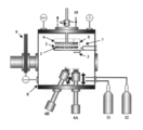
- Example of this invention it is a figure which shows notionally the structure of the combinatorial sputter coating system used in order to produce a B non-addition zinc oxide thin film and a B addition zinc oxide thin film.
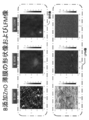
- the shape image and LFM (lateral force microscope) of B non-added zinc oxide thin film and B added zinc oxide thin film produced by changing the high frequency power to the B target in three ways of 0 W, 80 W and 120 W
- FIG. 2 shows the shape image of the same B non-addition zinc oxide thin film and B addition zinc oxide thin film as FIG. 2, and a vertical direction and a horizontal direction PFM (piezo-response force microscope) image.
- FIG. 1 shows notionally the structure of the combinatorial sputter coating system used in order to produce a B non-addition zinc oxide thin film and a B addition zinc oxide thin film.
- the shape image and LFM lateral force microscope
- FIG. 3 is a view showing longitudinal and lateral PFM images and LFM images of the same B-undoped zinc oxide thin film and B-doped zinc oxide thin film as in FIG. 2.
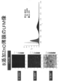
- FIG. 3 is an LFM image of the same B-undoped zinc oxide thin film and B-doped zinc oxide thin film as in FIG. 2 and a frequency distribution diagram of LFM measurement values for each of the B-undoped zinc oxide thin film and the B-doped zinc oxide thin film.
- FIG. 3 is a frequency distribution diagram of lateral PFM images and lateral PFM measurement values of the same B-undoped zinc oxide thin film and B-doped zinc oxide thin film as in FIG. 2.
- FIG. 3 is a frequency distribution diagram of longitudinal PFM images and lateral PFM measurement values of the same B-undoped zinc oxide thin film and B-doped zinc oxide thin film as in FIG. 2.
- the polarization of domains (crystal grains) constituting the zinc oxide thin film shows various aspects depending on the film forming conditions.
- the zinc oxide thin film is polarized in both the direction horizontal to the film surface and the direction perpendicular to the film surface, and the polarization magnitude in each direction is less than a certain value at 90% or more of the measurement points.
- the low-friction coating of the present invention exhibits vertical and horizontal piezo polarizations perpendicular to the film surface, and 90% of the measurement points when measured using a piezo response force microscope.
- it is characterized in that it is composed of a boron-added zinc oxide thin film whose longitudinal piezoelectric polarization is within 150 pm and whose lateral piezoelectric polarization is within 100 pm.
- the measurement points are preferably 60,000 or more.
- the composition ratio (mass ratio) of boron (B) is preferably 5 to 30%. If the boron content is within the above range, it can contribute to a significant reduction in frictional force.
- the “low friction coating” refers to a coating composed of a B-added zinc oxide thin film in which the frictional force is reduced by 40% or more by adding B to a zinc oxide thin film not containing B.
- the B-added zinc oxide thin film includes both cases where the zinc oxide thin film contains boron (B) atoms themselves and when boron (B) is contained as an oxide.
- the B-doped zinc oxide coating exhibits piezo polarization in both the vertical direction (direction perpendicular to the coating film surface) and the lateral direction (direction parallel to the film surface), and in each direction at 90% or more of the measurement points. It has been found that the friction of nanometer order is remarkably reduced when the magnitude of the piezo polarization is below a certain value.
- boron (B) is doped after adjusting the film forming conditions to obtain a B-added zinc oxide thin film.
- the film forming method it is preferable to use reactive sputtering.
- B Boron (B), which is an insulating material, segregates at the boundary of the domain of the B-added zinc oxide thin film produced in this manner, whereby the crystal grains constituting the zinc oxide thin film are electrically insulated from each other.
- the electric charge that appears on the surface by piezo polarization is locally strengthened, and a strong electric repulsion continues.
- the addition of B also improves the uniformity of polarization in the vertical direction and the horizontal direction for each crystal grain. In this way, polarization that is electrically isolated at the nano level is uniformly distributed on the surface of the film, so that minute contact points on the order of nanometers move on the surface and are adjacent to one crystal grain.
- the transverse polarization may be smaller than the longitudinal polarization, but if the longitudinal piezo polarization does not appear, the effect of reducing friction is hardly seen.
- the longitudinal and lateral piezopolarization measurements of the B-undoped zinc oxide thin film and the B-doped zinc oxide thin film were measured on the film surface with a probe having a very small tip, such as a scanning microscope (SPM).
- a piezo-response force microscope (PFM) was used to measure the deformation (length of extension and contraction) appearing at the point where the voltage was applied by applying a reverse piezo effect.
- PFM piezo-response force microscope
- the measurement of friction of nanometer order has the same configuration as a contact mode atomic force microscope (AFM), and a horizontal force microscope (lateral force microscope, which observes the twist generated when the probe is slid) This was also performed using a friction force microscope (hereinafter referred to as LFM).
- LFM friction force microscope
- friction is evaluated by applying a load of about several nN to several hundred nN using a probe having a probe diameter of about 20 to 40 nm.
- the sliding distance of the probe can be variously set up to about 50 nm to 150 ⁇ m depending on the application. In the following examples, the sliding distance was 2 ⁇ m. If the sliding distance of the probe at the time of LFM measurement is set to about 2 ⁇ m, it is sufficient for measurement of friction on the order of nanometers (that is, friction in a region having a size of less than 1 ⁇ m).
- the substrate after ultrasonic cleaning is fixed to the sample holder substrate of the combinatorial sputter coating system originally developed by the present inventors, and evacuated until the ultimate pressure (base pressure) becomes 5.0 ⁇ 10 ⁇ 5 Pa or less.
- base pressure base pressure
- coating was started, and a zinc oxide thin film or a zinc oxide thin film to which B was added was produced on a substrate by a reactive sputtering process in which zinc was sputter-evaporated in an oxygen atmosphere.
- the target-sample distance was 55 mm.
- Fig. 1 shows a conceptual diagram of the structure of the combinatorial sputter coating system used.
- a holder 2 that holds the substrate 1
- a shutter 3 that holds the substrate 1
- a magnetron sputtering source 4 (4 ⁇ / b> A, 4 ⁇ / b> B)
- a heater unit 5 that heats the substrate 1
- a cooling unit 6 that cools the substrate 1
- a quartz crystal microbalance 7 for monitoring the thickness of the sputtered thin film on 1 is disposed in the vacuum chamber 8.
- a control gate valve 9 is disposed in a passage to a vacuum pump (TMP + RP) that evacuates the inside of the vacuum chamber 8.
- TMP + RP vacuum pump
- FIG. Zn two sets of magnetron sputtering sources 4 are shown in FIG. Zn and B are attached to the magnetron sputter sources 4A and 4B, respectively.
- B 80 W and B: 120 W in the preparation of the B-doped zinc oxide thin film described later, B is used in addition to Zn as a target, and these two types of targets are attached to each magnetron sputtering source and sputtered simultaneously. went.
- Non-Patent Documents 2, 4, and 5 can be referred to if necessary. .
- the load coefficient friction and wear test apparatus (Shinto Kagaku Co., Ltd.) was used for measuring the friction coefficient ( ⁇ ).
- the measurement conditions were normal temperature / atmosphere environment, counterpart indenter material SUS304 and sapphire, indenter material size 3 mm ⁇ , applied load 0.12 N, indenter sliding distance 10 mm, and number of sliding times 200.
- the evaluation results of the piezo characteristics shown in FIGS. 3, 4, 6 and 7 were measured using an apparatus (model number: MFP-3D) manufactured by Oxford Asylum Research.
- the cantilever used with the apparatus is OMCL-RC800PB-1, and the probe used is a SiN cantilever with an Au coating (spring constant is 0.82 N / m, resonance frequency is 66 Hz).
- two sets of magnetron sputter sources are provided so that sputtering can be performed simultaneously from two types of targets.
- Zn is used as a target.
- a zinc oxide thin film having a thickness of 2 ⁇ m was formed on a stainless steel SUS440C substrate by reactive sputtering.
- a mixed gas of argon (Ar) and oxygen (O 2 ) is used as the sputtering gas, and the O 2 partial pressure ratio is 40%, 50%, 60%, 70%, 80%, 90%, and 100%.
- Seven types of zinc oxide thin films were prepared by changing the thickness. The crystal grain size on these films was measured and found to be 40-60 nm.
- the high frequency power is fixed to 100 W on the side where the Zn target is attached, while the high frequency power is 80 W and 120 W on the side where the B target is attached.
- the B addition amount was changed.
- the case where the high frequency power on the B target side is 0 W is also described. This is because a sample for comparison called a zinc oxide thin film to which B is not added is prepared. Indicates that the source has been stopped.
- the crystal grain size in the B-added zinc oxide thin film was 20 to 50 nm.
- the composition ratio (mass ratio) of B in the B-added zinc oxide thin film was 13.8% to 22.8%.
- FIG. 2 shows three samples prepared in this manner, namely B: 0W (B-undoped zinc oxide thin film) and B: 80W and B: 120W (the high frequency power of the B target side magnetron sputter source is 80W and 120W, respectively.
- the shape image that is, an image obtained by measuring the surface irregularities by AFM
- the LFM image are shown.
- the sliding distance for LFM measurement was 2 ⁇ m.
- B: 0W (B-undoped zinc oxide thin film) unevenness with a lateral size of about 100 nm to several tens of nm and a height exceeding 10 nm is distributed on one surface.
- the LFM image shows a similar granular pattern, and the friction on the order of nanometers is also at a fairly high level on average.
- each unevenness corresponds to a domain.
- the shape images of the B: 80W and B: 120W samples which are B-added zinc oxide thin films do not show the presence of clear irregularities like the B: 0W sample, and the LFM image also covers the entire surface. It shows very low and even friction.
- the horizontal and vertical PFM images and shape images of these three types of samples were compared.
- the B-undoped zinc oxide thin film showed large variations corresponding to the shape and size of the unevenness of the shape image in both the vertical PFM and the horizontal PFM, whereas in the B-doped zinc oxide thin film, both Small vertical and horizontal PFM variations were shown compared to the B-free zinc oxide thin film.
- the horizontal direction PFM indicates a small value here, but is a certain finite value that is not zero.
- FIG. 4 shows a comparison of the vertical and horizontal PFM images and LFM images of these three types of samples.
- the zinc additive-free zinc oxide thin film shows a large variation corresponding to the unevenness on the surface shown in the shape image of FIG. 3 etc. in both the vertical direction and the horizontal direction PFM.
- the LFM image also corresponds to the shape image, and a high level of friction appears.
- the two samples of the B-added zinc oxide thin film both show vertical and horizontal PFM images with little variation, and the corresponding LFM images also show uniform and low friction.
- the horizontal axis shows the voltage that is the reading value of the LFM measurement (note that the magnitude of the probe twist is read here as a voltage. In other words, the higher the voltage, the more the probe twists during sliding. Large, indicating that the friction is large after all), and the vertical axis indicates the frequency with which each voltage was read.
- the zinc oxide thin film with no B added has large friction over the entire surface, and the magnitude of the friction varies over a wide range.
- any sample shows low friction and small variation over the entire surface, that is, a uniform low friction state.
- a distribution map was created that clearly shows the size and variation of the lateral PFM measurement results of these three types of samples.
- the lateral PFM images of the three types of samples are shown on the left side of FIG. 6, and the distribution diagram of the PFM measurement results is shown on the right side.
- the horizontal axis indicates the length, which is a reading value of the PFM measurement, by pm
- the vertical axis indicates the frequency at which each length is read.
- the Z-doped zinc oxide thin film has a wide range of lateral PFM over the entire surface.
- the PFM measurement result is not 0 over the entire surface of any sample, but the value is small and the variation is small.
- a coating having a very small friction on the order of nanometers can be realized, so that a very small contact surface (contact between the movable member and another member that this member contacts)
- the size of the region is about 1 nm to 200 ⁇ m). For example, it is expected to be used for a micro mechanism member in a micromachine.
Landscapes
- Chemical & Material Sciences (AREA)
- Engineering & Computer Science (AREA)
- Mechanical Engineering (AREA)
- Organic Chemistry (AREA)
- Chemical Kinetics & Catalysis (AREA)
- Computer Hardware Design (AREA)
- Microelectronics & Electronic Packaging (AREA)
- Materials Engineering (AREA)
- Metallurgy (AREA)
- General Chemical & Material Sciences (AREA)
- Oil, Petroleum & Natural Gas (AREA)
- Physical Vapour Deposition (AREA)
- Micromachines (AREA)
Abstract
Description
ここで、前記可動部材と前記他の部材とが接触する領域のサイズは1nm~200μmであってよい。
また、B添加酸化亜鉛薄膜は、酸化亜鉛薄膜中にホウ素(B)原子そのものが含有される場合と、ホウ素(B)が酸化物として含有される場合の両方のケースを含んでいる。
先ず、図1に構成を概念的に示すコンビナトリアルスパッタコーティングシステムを使用して、以下の表1に示す成膜条件で、Bを添加しない酸化亜鉛薄膜を作製した。

スパッタリングガス中のO2分圧を上げていくと、B未添加酸化亜鉛薄膜のPFM像(図示せず)が分圧比60%付近でPFMのバラツキが急に小さくなって一様な膜が形成されていることがわかり、またPFM測定結果のヒストグラムでもO2の分圧比が60%~80%の範囲でヒストグラム(図示せず)の形状が最も急峻になることが確認された。この予備的実験の結果に基づいて、スパッタガス中のArとO2の分圧比を40%:60%に固定し、上で行った反応性スパッタによる酸化亜鉛薄膜作製中にBターゲットからBを同時に供給することで、B添加酸化亜鉛薄膜を作製した。その製膜条件を以下の表2にまとめて示す。

2 ホルダー
3 シャッター
4(4A、4B) マグネトロンスパッタソース
5 ヒーターユニット
6 冷却ユニット
7 水晶振動子マイクロバランス
8 真空槽
9 制御ゲートバルブ
10 冷却水
11 Ar
12 反応ガス
Claims (3)
- 膜面に対して垂直な縦方向および水平な横方向のピエゾ分極を発現しており、測定点の90%以上で、前記縦方向のピエゾ分極の大きさが150pm以内でありかつ横方向のピエゾ分極の大きさが100pm以内であるホウ素添加酸化亜鉛薄膜からなる低摩擦コーティング。
- 請求項1に記載の低摩擦コーティングを、可動部材及び前記可動部材が接触する他の部材の少なくとも一方に施したマイクロマシン。
- 前記可動部材と前記他の部材とが接触する領域のサイズは1nm~200μmである請求項2に記載のマイクロマシン。
Priority Applications (3)
| Application Number | Priority Date | Filing Date | Title |
|---|---|---|---|
| JP2017520794A JP6548130B2 (ja) | 2015-05-26 | 2016-05-25 | ホウ素添加酸化亜鉛薄膜からなる低摩擦コーティングおよびマイクロマシン |
| EP16800079.2A EP3305939A4 (en) | 2015-05-26 | 2016-05-25 | FRAME-FREE COATING OF ZINC OXIDE THIN LAYER WITH BORED ADDITION AND MICROMATIC MACHINE |
| US15/576,376 US10343893B2 (en) | 2015-05-26 | 2016-05-25 | Low friction coating formed of boron-doped zinc oxide thin film and micromachine |
Applications Claiming Priority (2)
| Application Number | Priority Date | Filing Date | Title |
|---|---|---|---|
| JP2015-105970 | 2015-05-26 | ||
| JP2015105970 | 2015-05-26 |
Publications (1)
| Publication Number | Publication Date |
|---|---|
| WO2016190375A1 true WO2016190375A1 (ja) | 2016-12-01 |
Family
ID=57393485
Family Applications (1)
| Application Number | Title | Priority Date | Filing Date |
|---|---|---|---|
| PCT/JP2016/065521 Ceased WO2016190375A1 (ja) | 2015-05-26 | 2016-05-25 | ホウ素添加酸化亜鉛薄膜からなる低摩擦コーティングおよびマイクロマシン |
Country Status (4)
| Country | Link |
|---|---|
| US (1) | US10343893B2 (ja) |
| EP (1) | EP3305939A4 (ja) |
| JP (1) | JP6548130B2 (ja) |
| WO (1) | WO2016190375A1 (ja) |
Cited By (1)
| Publication number | Priority date | Publication date | Assignee | Title |
|---|---|---|---|---|
| WO2023090275A1 (ja) | 2021-11-16 | 2023-05-25 | 出光興産株式会社 | 固体潤滑材、摺動部材及び固体潤滑材の形成方法 |
Families Citing this family (1)
| Publication number | Priority date | Publication date | Assignee | Title |
|---|---|---|---|---|
| US12091313B2 (en) | 2019-08-26 | 2024-09-17 | The Research Foundation For The State University Of New York | Electrodynamically levitated actuator |
Citations (4)
| Publication number | Priority date | Publication date | Assignee | Title |
|---|---|---|---|---|
| JP2004052022A (ja) * | 2002-07-17 | 2004-02-19 | National Institute For Materials Science | 低摩擦材料 |
| US20120070672A1 (en) * | 2010-09-17 | 2012-03-22 | Guardian Industries Corp. | Coated article having boron doped zinc oxide based seed layer with enhanced durability under functional layer and method of making the same |
| US20140202851A1 (en) * | 2013-01-22 | 2014-07-24 | Solar Applied Materials Technology Corp. | Boron-doped zinc oxide sputtering target and its application |
| JP2014152387A (ja) * | 2013-02-13 | 2014-08-25 | Solar Applied Materials Technology Corp | ボロンをドープした亜鉛酸化物スパッタリングターゲット及びその使用 |
Family Cites Families (3)
| Publication number | Priority date | Publication date | Assignee | Title |
|---|---|---|---|---|
| JPS5516554A (en) * | 1978-07-21 | 1980-02-05 | Toko Inc | Manufacture of thin film of zinc oxide |
| JP2007154315A (ja) | 2007-01-24 | 2007-06-21 | National Institute For Materials Science | 真空中での低摩擦化構造 |
| JP2014224960A (ja) | 2013-01-10 | 2014-12-04 | 株式会社リコー | クリーニング装置、プロセスカートリッジ、及び画像形成装置 |
-
2016
- 2016-05-25 WO PCT/JP2016/065521 patent/WO2016190375A1/ja not_active Ceased
- 2016-05-25 JP JP2017520794A patent/JP6548130B2/ja active Active
- 2016-05-25 US US15/576,376 patent/US10343893B2/en active Active
- 2016-05-25 EP EP16800079.2A patent/EP3305939A4/en not_active Withdrawn
Patent Citations (4)
| Publication number | Priority date | Publication date | Assignee | Title |
|---|---|---|---|---|
| JP2004052022A (ja) * | 2002-07-17 | 2004-02-19 | National Institute For Materials Science | 低摩擦材料 |
| US20120070672A1 (en) * | 2010-09-17 | 2012-03-22 | Guardian Industries Corp. | Coated article having boron doped zinc oxide based seed layer with enhanced durability under functional layer and method of making the same |
| US20140202851A1 (en) * | 2013-01-22 | 2014-07-24 | Solar Applied Materials Technology Corp. | Boron-doped zinc oxide sputtering target and its application |
| JP2014152387A (ja) * | 2013-02-13 | 2014-08-25 | Solar Applied Materials Technology Corp | ボロンをドープした亜鉛酸化物スパッタリングターゲット及びその使用 |
Non-Patent Citations (2)
| Title |
|---|
| GOTO MASAHIRO ET AL.: "Reduction in Frictional Force of ZnO Coatings in a Vacuum", JAPANESE JOURNAL OF APPLIED PHYSICS, vol. 47, no. 12, 19 December 2008 (2008-12-19), pages 8914 - 8916, XP055332093 * |
| See also references of EP3305939A4 * |
Cited By (1)
| Publication number | Priority date | Publication date | Assignee | Title |
|---|---|---|---|---|
| WO2023090275A1 (ja) | 2021-11-16 | 2023-05-25 | 出光興産株式会社 | 固体潤滑材、摺動部材及び固体潤滑材の形成方法 |
Also Published As
| Publication number | Publication date |
|---|---|
| US20180155183A1 (en) | 2018-06-07 |
| JP6548130B2 (ja) | 2019-07-24 |
| EP3305939A4 (en) | 2019-03-13 |
| JPWO2016190375A1 (ja) | 2018-03-08 |
| US10343893B2 (en) | 2019-07-09 |
| EP3305939A1 (en) | 2018-04-11 |
Similar Documents
| Publication | Publication Date | Title |
|---|---|---|
| Cui et al. | Mechanical and tribological properties of Ti-DLC films with different Ti content by magnetron sputtering technique | |
| Ramana et al. | Growth behavior, lattice expansion, strain, and surface morphology of nanocrystalline, monoclinic HfO2 thin films | |
| Shibata et al. | Fabrication and characterization of diamond AFM probe integrated with PZT thin film sensor and actuator | |
| Matlak et al. | Friction properties of amorphous carbon ultrathin films deposited by filtered cathodic vacuum arc and radio-frequency sputtering | |
| CN110396661A (zh) | 调节ecr离子照射密度控制石墨烯纳晶碳膜生长的方法 | |
| WO2016190375A1 (ja) | ホウ素添加酸化亜鉛薄膜からなる低摩擦コーティングおよびマイクロマシン | |
| Fu et al. | Optimization of the annealing process and nanoscale piezoelectric properties of (002) AlN thin films | |
| Hofer-Roblyek et al. | Linking erosion and sputter performance of a rotatable Mo target to microstructure and properties of the deposited thin films | |
| JP5891464B2 (ja) | ZnOコーティング、それを作製する方法及びそれの利用方法 | |
| Ding et al. | Microstructure evolution and mechanical properties of Al doped ta-C films prepared by filtered cathodic vacuum arc | |
| Liu et al. | Surface roughness, mechanical and tribological properties of ultrathin tetrahedral amorphous carbon coatings from atomic force measurements | |
| Xie et al. | Substrate angle‐induced fully c‐axis orientation of AlN films deposited by off‐normal DC sputtering method | |
| CN112030125A (zh) | 一种ods金属薄膜材料的制备方法 | |
| Akdogan et al. | SmCo-based MFM probes with high switching fields | |
| Choi et al. | Characterization of diamond-like carbon thin films prepared by a microwave plasma enhanced chemical vapor deposition method | |
| CN112176296B (zh) | 一种自组装可调间隙的金纳米薄膜制备方法 | |
| US11873551B2 (en) | Ultra-flat and low-friction metallic glass film and a method for preparing the same | |
| Vladoiu et al. | Structural and Mechanical Properties of Nanostructured C‐Ag Thin Films Synthesized by Thermionic Vacuum Arc Method | |
| Kim et al. | Effect of sputtering parameters on molybdenum disulfide thin films synthesized by radio frequency magnetron sputtering and electron-beam irradiation | |
| Joulaei et al. | Experimental investigation of the adhesion force of single and double‐layer coatings on MEMS surfaces | |
| CN105043904A (zh) | 一种基于纳米压入测试技术的超薄铜膜疲劳失效预测方法 | |
| Tien et al. | Effects of ion energy on internal stress and optical properties of ion-beam sputtering Ta2O5 films | |
| Liskiewicz et al. | In situ accelerated micro-wear—A new technique to fill the measurement gap | |
| Li et al. | RF nano switch based on single crystalline graphene | |
| CN113078261B (zh) | 一种Sn-Se系列超晶格相变存储材料及其制备方法 |
Legal Events
| Date | Code | Title | Description |
|---|---|---|---|
| 121 | Ep: the epo has been informed by wipo that ep was designated in this application |
Ref document number: 16800079 Country of ref document: EP Kind code of ref document: A1 |
|
| ENP | Entry into the national phase |
Ref document number: 2017520794 Country of ref document: JP Kind code of ref document: A |
|
| WWE | Wipo information: entry into national phase |
Ref document number: 15576376 Country of ref document: US |
|
| NENP | Non-entry into the national phase |
Ref country code: DE |
|
| WWE | Wipo information: entry into national phase |
Ref document number: 2016800079 Country of ref document: EP |