WO2016178406A1 - 薄膜および薄膜形成方法 - Google Patents
薄膜および薄膜形成方法 Download PDFInfo
- Publication number
- WO2016178406A1 WO2016178406A1 PCT/JP2016/063312 JP2016063312W WO2016178406A1 WO 2016178406 A1 WO2016178406 A1 WO 2016178406A1 JP 2016063312 W JP2016063312 W JP 2016063312W WO 2016178406 A1 WO2016178406 A1 WO 2016178406A1
- Authority
- WO
- WIPO (PCT)
- Prior art keywords
- thin film
- discharge
- substrate
- gas
- grain boundary
- Prior art date
- Legal status (The legal status is an assumption and is not a legal conclusion. Google has not performed a legal analysis and makes no representation as to the accuracy of the status listed.)
- Ceased
Links
Images





Classifications
-
- B—PERFORMING OPERATIONS; TRANSPORTING
- B32—LAYERED PRODUCTS
- B32B—LAYERED PRODUCTS, i.e. PRODUCTS BUILT-UP OF STRATA OF FLAT OR NON-FLAT, e.g. CELLULAR OR HONEYCOMB, FORM
- B32B5/00—Layered products characterised by the non- homogeneity or physical structure, i.e. comprising a fibrous, filamentary, particulate or foam layer; Layered products characterised by having a layer differing constitutionally or physically in different parts
- B32B5/14—Layered products characterised by the non- homogeneity or physical structure, i.e. comprising a fibrous, filamentary, particulate or foam layer; Layered products characterised by having a layer differing constitutionally or physically in different parts characterised by a layer differing constitutionally or physically in different parts, e.g. denser near its faces
-
- C—CHEMISTRY; METALLURGY
- C23—COATING METALLIC MATERIAL; COATING MATERIAL WITH METALLIC MATERIAL; CHEMICAL SURFACE TREATMENT; DIFFUSION TREATMENT OF METALLIC MATERIAL; COATING BY VACUUM EVAPORATION, BY SPUTTERING, BY ION IMPLANTATION OR BY CHEMICAL VAPOUR DEPOSITION, IN GENERAL; INHIBITING CORROSION OF METALLIC MATERIAL OR INCRUSTATION IN GENERAL
- C23C—COATING METALLIC MATERIAL; COATING MATERIAL WITH METALLIC MATERIAL; SURFACE TREATMENT OF METALLIC MATERIAL BY DIFFUSION INTO THE SURFACE, BY CHEMICAL CONVERSION OR SUBSTITUTION; COATING BY VACUUM EVAPORATION, BY SPUTTERING, BY ION IMPLANTATION OR BY CHEMICAL VAPOUR DEPOSITION, IN GENERAL
- C23C16/00—Chemical coating by decomposition of gaseous compounds, without leaving reaction products of surface material in the coating, i.e. chemical vapour deposition [CVD] processes
- C23C16/44—Chemical coating by decomposition of gaseous compounds, without leaving reaction products of surface material in the coating, i.e. chemical vapour deposition [CVD] processes characterised by the method of coating
- C23C16/50—Chemical coating by decomposition of gaseous compounds, without leaving reaction products of surface material in the coating, i.e. chemical vapour deposition [CVD] processes characterised by the method of coating using electric discharges
- C23C16/505—Chemical coating by decomposition of gaseous compounds, without leaving reaction products of surface material in the coating, i.e. chemical vapour deposition [CVD] processes characterised by the method of coating using electric discharges using radio frequency discharges
-
- H—ELECTRICITY
- H05—ELECTRIC TECHNIQUES NOT OTHERWISE PROVIDED FOR
- H05H—PLASMA TECHNIQUE; PRODUCTION OF ACCELERATED ELECTRICALLY-CHARGED PARTICLES OR OF NEUTRONS; PRODUCTION OR ACCELERATION OF NEUTRAL MOLECULAR OR ATOMIC BEAMS
- H05H1/00—Generating plasma; Handling plasma
- H05H1/24—Generating plasma
- H05H1/26—Plasma torches
Definitions
- the present disclosure relates to a thin film formed on the surface of a substrate and a method for forming the thin film. More specifically, a thin film such as a carbon thin film or a metal oxide thin film having an inclined structure with high adhesion to the substrate, and the thin film under atmospheric pressure or pressure near atmospheric pressure (hereinafter, also referred to as atmospheric pressure). It is related with the method of forming a thin film on the base-material surface using the discharge plasma produced
- a thin film By forming a thin film on the surface of a base material such as a polymer or a metal material, high functionality (for example, high hardness, scratch resistance or high gas barrier property) can be applied to the base material as a bulk at low cost, resource saving and simple. Etc.) has been widely used in practice.
- a base material such as a polymer or a metal material
- high functionality for example, high hardness, scratch resistance or high gas barrier property
- Etc. has been widely used in practice.
- technology for coating an inorganic thin film made of a metal oxide such as silicon oxide or aluminum oxide on the surface of a plastic substrate or metal substrate has been developed, and a technology that imparts functions such as surface protection, gas barrier properties, and cosmetics. Is widely used (see, for example, Patent Document 1).
- inorganic thin films are conventionally formed by physical vapor deposition such as sputtering under vacuum, ion plating or vacuum deposition, or plasma CVD where chemical species are activated by plasma excited by high frequency or microwave.
- a method of forming a film by the (Chemical Vapor Deposition) method is common. In any case, film formation in a low pressure region from high vacuum to medium vacuum is essential. In the film formation in the low pressure region, the active species that are the raw materials of the film rarely collide with other molecules or active species in the gas phase, so that the formed inorganic thin film must be a uniform amorphous film. It is a feature.
- the formed thin film is uniform in the thickness direction, for example, in the case of a thin film having functions such as high hardness, wear resistance or high gas barrier properties, the characteristics of the base material at the interface with the base material The difference was too large, and peeling might occur, and there was a problem in adhesion.
- Patent Document 5 and Patent Document 6 disclose a method for producing a diamond-like carbon thin film by dielectric barrier discharge under atmospheric pressure using a high voltage pulse power source. In general, glow discharge is used in the atmospheric pressure plasma CVD method using dielectric barrier discharge (see, for example, Non-Patent Document 1).
- Japanese Patent Laid-Open No. 11-348171 Japanese Patent Laid-Open No. 9-272567 JP 2008-94447 A JP 2010-242225 A Japanese Patent Laid-Open No. 11-12735 JP 2010-208277 A
- Patent Document 3 the method of increasing the adhesion to the base material by the laminated structure of thin films necessitates the formation of a plurality of thin films having different compositions and structures. There was a problem that the cost required for the production was large.
- Non-Patent Document 1 the method using dielectric barrier discharge as described in Patent Document 5 or Patent Document 6 maintains the atmospheric pressure glow discharge to obtain a uniform plasma state at a low temperature.
- functions such as the density of the thin film formed, the hardness, and gas barrier property, were low compared with the vacuum method (plasma CVD method using a vacuum).
- active species often collide with other molecules or active species in the gas phase, so that the particles are different from each other unlike a thin film obtained by the vacuum method. It has a non-uniform structure having a grain boundary formed by bonding.
- the collision energy to the substrate is also smaller than that of the vacuum method, and as a result, the adhesion to the substrate is also lowered.
- the electric field strength is increased in order to obtain a high-density plasma at atmospheric pressure, ionization is abruptly derived.
- the avalanche grows linearly and a streamer discharge is generated.
- streamer discharge occurs, the plasma becomes non-uniform, and further, the generation of thermoelectrons shifts to arc discharge to become high-temperature plasma, so that damage to the substrate increases and it is difficult to form a thin film. For this reason, conventionally, it has been preferable to suppress the occurrence of streamer discharge in the atmospheric pressure plasma CVD method.
- the present disclosure solves the above-described problems, has high functionality (hardness, wear resistance, etc.) equal to or higher than that of a thin film obtained by a plasma CVD method using vacuum on the surface of the base material, and the base material
- An object of the present invention is to provide a thin film having high adhesiveness and a method for forming the thin film.
- the thin film according to the present invention is a thin film provided on the surface of a substrate.
- the thin film has a grain boundary density that decreases continuously or intermittently from the inner surface of the thin film toward the outer surface of the thin film.
- the innermost region that has an inclined structure and is in contact with the surface of the substrate of the thin film has a grain boundary structure in which the grain boundary has a grain size of 10 to 30 nm.
- the thin film forming method includes a pair of counter electrodes including a first electrode connected to a power source for applying a voltage and a grounded second electrode, and a reaction gas and a discharge gas between the pair of counter electrodes. And a gas supply path for supplying a mixed gas, wherein the opposing surface of the first electrode is covered with a solid dielectric, in a thin film forming method using a film forming apparatus, on the opposing surface of the second electrode, A step of installing a base material having a surface resistance in the range of 10 ⁇ 8 to 10 3 ohm / sq, and the mixed gas from the gas supply path between the pair of counter electrodes under a pressure at or near atmospheric pressure. And supplying a voltage from the power source to generate a streamer discharge to form a thin film on the surface of the substrate by plasma CVD.
- the discharge gas is preferably at least one of helium, argon, nitrogen, or a mixture thereof.
- the discharge gas is composed of helium or helium and argon, and the composition of the discharge gas includes helium in a range of 40 to 100% as a volume ratio in a standard state.
- Argon is preferably contained in the range of 60 to 0%.
- the surface of the base material has high functionality (hardness, wear resistance, etc.) equal to or higher than that of a thin film obtained by a plasma CVD method using a vacuum, and adhesion to the base material.
- a high thin film and a method for forming the thin film can be provided.
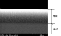
- FIG. 1 is a scanning electron microscope image of a thin film cross section according to the present embodiment.
- the thin film according to the present embodiment is a thin film provided on the surface of a substrate.
- the thin film has a continuous or intermittent grain boundary density from the inner surface of the thin film toward the outer surface of the thin film.
- the innermost region in contact with the surface of the substrate of the thin film has a grain boundary structure in which the grain boundary has a grain size of 10 to 30 nm.
- the type of the thin film is not particularly limited, and is, for example, a carbon-based thin film, a metal oxide thin film, or a silicon-based thin film.
- the thickness of the thin film is preferably 100 to 800 nm, and more preferably 200 to 600 nm.
- the innermost region is the deepest portion of the thin film as viewed from the outer surface, and includes the inner surface of the thin film (the surface on the side in contact with the thin film substrate).
- the innermost region preferably includes a region of up to 30 nm in the direction from the inner surface of the thin film to the outer surface of the thin film (the surface opposite to the side in contact with the substrate of the thin film) in the thickness direction of the thin film.
- the outermost region is the shallowest portion of the thin film as viewed from the outer surface, and includes the outer surface of the thin film.
- the outermost region preferably includes a region of up to 30 nm in the direction from the outer surface of the thin film to the substrate in the thickness direction of the thin film.
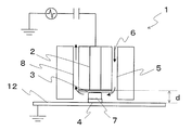
- the thin film shown in FIG. 1 can be formed by, for example, a film forming apparatus shown in FIG. Of the counter electrodes 2 and 12 made of copper, for example, disposed in parallel to each other, the solid dielectric 3 is disposed on the facing surface side of the counter electrode 2.
- the solid dielectric 3 for example, a plastic such as polytetrafluoroethylene, polyethylene terephthalate or polyethylene, glass, or a metal oxide such as alumina can be used.
- a base material 4 is disposed between the solid dielectric 3 and the other counter electrode 12.
- the mixed gas 6 containing the reaction gas component is supplied to the gap between the counter electrodes 2 and 12 through the gas supply path 5 at a predetermined flow rate.
- the mixed gas 6 is turned into plasma by a high-frequency voltage applied between the counter electrodes 2 and 12, and becomes a plasma mixed gas 7.
- a part of the reactive gas component contained in the plasmified mixed gas 7 is deposited on the surface of the substrate 4 to form a thin film (not shown).
- the mixed gas 6 that has passed between the counter electrodes 2 and 12 and has consumed a part of the reaction gas component is discharged out of the system through the exhaust path 8.
- the thin film in FIG. 1 is a thin film formed by an atmospheric pressure plasma CVD method using streamer discharge (hereinafter also referred to as “atmospheric pressure method (streamer discharge)”).
- the thin film shown in FIG. 1 was formed as follows. That is, the distance d between the opposing electrodes 2 and 12 is 4 mm, and a silicon substrate (surface resistance 260 ohm / sq, thickness 0.38 mm) is disposed on the opposing surface of the electrode 12 as the substrate 4, and the pressure is 100 kPa.
- a mixed gas containing methane (CH 4 ) 400 mL / min as a reaction gas and helium (He) 4 L / min and argon (Ar) 1 L / min as a discharge gas is supplied from a gas supply path, and the frequency A pulsed voltage was applied under power supply conditions of 30 kHz, a pulse width of 5 ⁇ s, and a voltage of 7 kV to generate a discharge to form a thin film having a thickness of 500 nm on the surface of the substrate 4.
- the film formation time was 250 s.
- the counter electrodes 2 and 12 are made of copper.
- the structure of the thin film formed by the atmospheric pressure method has a grain boundary structure in which grain boundaries are clearly formed in the innermost region in contact with the surface of the substrate.
- the grain boundary grain size in the innermost region was in the range of 10-30 nm.
- the grain boundary grain size is the vertical diameter of the outer edge of the integrated grain boundary structure when the grain boundary structure can be confirmed by shading when the magnification is 40000 times in cross-sectional observation by SEM or TEM. It is obtained as an average value of the horizontal diameter.
- the thin film showed a structure in which the grain boundary gradually becomes unclear and approaches a uniform amorphous structure as it approaches the outermost region of the thin film.
- the thin film according to the present embodiment has an inclined structure in which the grain boundary density decreases continuously or intermittently from the inner surface of the thin film toward the outer surface of the thin film.
- Grain boundary density (dimensionless number) is a unit area between the grain boundary structure confirmed by shading and the continuous amorphous part between the grain boundary structures at a magnification of 40000 times of cross-sectional observation in SEM or TEM. Is the area ratio.
- the grain boundary had a grain boundary structure with a grain size of 10 to 30 nm.
- the region (outermost region) up to 30 nm in the direction from the outer surface of the thin film toward the base material had an amorphous structure. In the region between the innermost region and the outermost region, a portion having a grain boundary structure and a portion having an amorphous structure were mixed.
- FIG. 1 shows a form in which the outermost region of the thin film has an amorphous structure, but in the present embodiment, the outermost region of the thin film may have a grain boundary structure.
- the grain boundary grain size in the outermost region is preferably larger than the grain boundary grain size in the innermost region.
- a thin film in which the outermost region has a grain boundary structure can be obtained, for example, by stopping when a predetermined film thickness is reached in the formation of the thin film.
- the predetermined film thickness varies depending on the film forming conditions such as the type of base material, the type of mixed gas, the gas flow rate, and the power supply conditions of the film forming apparatus, but is, for example, 100 to 250 nm in the thin film forming conditions of FIG.
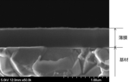
- FIG. 2 is a scanning electron microscope image of a cross section of a thin film formed by a vacuum plasma CVD method (hereinafter sometimes referred to as “vacuum method”).
- the thin film shown in FIG. 2 was formed as follows. That is, using a parallel plate method high-frequency plasma CVD apparatus, using acetylene (C 2 H 2 ) as a reactive gas under a pressure of 0.1 Torr (13.3 Pa), under conditions of a high-frequency power of 200 W and a frequency of 13.56 MHz. Film formation was performed. The film thickness of the thin film was 500 nm and the film formation time was 100 s.
- FIG. 3 is a scanning electron microscope image of a cross section of a thin film formed by an atmospheric pressure plasma CVD method using glow discharge (hereinafter sometimes referred to as “atmospheric pressure method (glow discharge)”).
- the thin film shown in FIG. 3 was formed as follows. That is, in the production of the thin film of FIG. 1, the distance between the counter electrodes is 1 mm, and a mixed gas containing acetylene (C 2 H 2 ) 20 mL / min as a reaction gas and nitrogen (N 2 ) 1 L / min as a discharge gas is used. It was fabricated in the same manner as the thin film of FIG. 1 except that the power supply conditions were changed to a frequency of 10 kHz, a pulse width of 5 ⁇ s, and a voltage of 18 kV. The thickness of the thin film was 800 nm and the film formation time was 50 s.
- 1 to 3 are images observed at a magnification of 40000 times.
- the structure of the thin film formed by the vacuum method has a uniform amorphous state throughout the thickness direction of the thin film, and did not show a structure forming a grain boundary.
- the structure of the thin film formed by the atmospheric pressure method has a clear grain boundary structure in which the grain boundary has a grain size of 50 to 100 nm over the entire thickness direction of the thin film. Was showing.
- the hardness of the thin film was 12 GPa by the atmospheric pressure method (streamer discharge), 3 GPa by the atmospheric pressure method (glow discharge), and 12 GPa by the vacuum method.
- the hardness was measured by performing a nanoindentation test using a Barcovic indenter according to ISO 14577-2002 using a nanoindenter system (“Nano Indenter G200” manufactured by Agilent Technologies), and measuring the indentation depth. Indentation hardness was calculated.
- the peel resistance of the thin film is determined by the cross-cut peel test (JIS K 5600-5-6: 1999 “General paint test method-Part 5: Mechanical properties of the coating film—Section 6: Adhesion (cross-cut method)”) ), In order from the best, the atmospheric pressure method (streamer discharge), the vacuum method, and the atmospheric pressure method (glow discharge). From this result, it can be seen that the grain boundary structure having a particle size of about 10 to 30 nm has higher adhesion at the interface between the base material and the thin film than the uniform amorphous structure having no grain boundary.
- the particle size is 50 nm or more, the kinetic energy is lost in the gas phase, so that the adhesion to the substrate is reduced as compared with the case where the particle size is 10 to 30 nm.
- the outermost region of the thin film has an amorphous structure as shown in FIGS.
- the thin film formed by the atmospheric pressure method streamer discharge
- has a gradient structure and therefore has high hardness characteristics and high adhesion characteristics equivalent to or higher than those obtained by the vacuum method. Admitted.
- the atmospheric pressure method is more rough than the atmospheric pressure method (glow discharge).
- the surface roughness was measured using a scanning probe microscope (“SPM-9700”, manufactured by Shimadzu Corporation) in accordance with JIS R 1683: 2007 “Method for measuring surface roughness of fine ceramic thin film by atomic force microscope”. did.
- the thin film according to this embodiment preferably has an inclined structure in which the hydrogen concentration increases as it approaches the outer surface of the thin film.
- the hydrogen concentration in the thin film can be measured by, for example, analyzing the depth direction of the thin film by secondary ion mass spectrometry (SIMS).
- the hydrogen concentration in the thin film may be estimated from the Raman analysis result.
- Raman spectroscopy is an analysis method that spectroscopically measures scattered light (Raman scattered light) emitted to a substance, and can analyze the composition and structure of the substance.
- the Raman spectrum of a typical DLC film is composed of a G band near 1500 cm ⁇ 1 and a D band near 1300 cm ⁇ 1 .
- log (N / S) or N / (N + S) is defined as a parameter that can be a qualitative analysis value of hydrogen concentration, where S is the Raman scattered light intensity at the peak position of the G band and N is the fluorescence component intensity. (For example, refer nonpatent literature 2.).
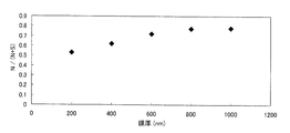
- a thin film was formed in the same manner as the thin film shown in FIG. 1 except that the thickness of the thin film shown in FIG. At this time, Raman analysis was performed every 200 nm of film thickness, and N / (N + S) was obtained. The relationship between the film thickness and N / (N + S) is shown in FIG.
- N / (N + S) was 0.5 at 200 nm and 0.75 at 800 nm. And up to 800 nm, N / (N + S) increased as it approached the outer surface of the thin film, and N / (N + S) was substantially constant above 800 nm. From this, it was confirmed that the thin film of the specimen 5 had an inclined structure in which the hydrogen concentration increased as it approached the outer surface of the thin film.
- N / (N + S) was about 0.9 to 1, and no gradient of hydrogen concentration was observed.
- the hydrogen concentration on the outer surface of the thin film was lower than that in the atmospheric method (glow discharge).
- N / (N + S) was about 0.6 to 0.7, and no gradient of hydrogen concentration was observed. From this, it was confirmed that in the atmospheric pressure method (streamer discharge), the hydrogen concentration on the outer surface of the thin film was comparable to that in the vacuum method. This result is consistent with the result of wear resistance evaluation.
- the wear resistance of the SiOx thin film obtained by the atmospheric pressure method is the highest. it was high. The reason for this is that the closer the thin film is to the surface, the more clearly the grain boundary becomes closer to a uniform amorphous structure.
- the hydrogen concentration in the outermost region increases compared to the innermost region, and the density increases accordingly. It is believed that having a graded property that declines increases slidability and cushioning, resulting in increased wear resistance.
- the thin film formation method according to the present embodiment includes a pair of counter electrodes 2 and 12 including a first electrode 2 connected to a power source to which a voltage is applied and a grounded second electrode 12, and a pair of counter electrodes 2 and 12.
- a gas supply path 5 for supplying a mixed gas containing a reaction gas and a discharge gas, and a facing surface of the first electrode 2 is covered with a solid dielectric 3 in a thin film forming method using a film forming apparatus 1
- the reaction gas is appropriately selected depending on the type of the thin film, and the present invention is not limited to this.
- the reaction gas is, for example, a compound containing carbon, hydrogen and / or oxygen, and is preferably any one of methane, ethane, propane, or a mixture thereof.
- the reaction gas is, for example, an organometallic compound and oxygen.
- the organometallic compound is, for example, trimethylaluminum or titanium tetraisopoloxide.
- the reaction gas is, for example, an organosilicon compound and oxygen.
- the organosilicon compound is, for example, trimethylsilane (TrMS), tetraethoxysilane (TEOS), tetramethoxysilane (TMOS), or hexamethyldisiloxane (HMDSO).
- TrMS trimethylsilane
- TEOS tetraethoxysilane
- TMOS tetramethoxysilane
- HMDSO hexamethyldisiloxane
- one reactive gas may be used alone, or two or more reactive gases may be mixed and used.
- the discharge gas it is preferable to use at least one kind of helium, argon or nitrogen, or a mixture thereof, and it is particularly preferable that helium is contained in a standard state of 40% or more, more preferably 60% or more.
- the discharge gas is composed of helium or helium and argon, and the composition of the discharge gas includes helium in a range of 40 to 100% as a standard volume ratio, and argon in a range of 60 to 0%. It is preferable to contain.
- one of the counter electrodes (upper electrode in FIG. 4) 2 is preferably applied with a high frequency voltage or a pulse voltage, and the other electrode (lower electrode in FIG. 4) 12 is grounded. ing.
- a mixed gas 6 containing a reactive gas that is a raw material for the thin film and a discharge gas that is ionized to generate discharge plasma is supplied between the opposing electrodes.
- the opposing surface of the opposing electrode 2 to which a voltage is applied is covered with a solid dielectric 3 such as alumina. When the discharge starts, the discharge voltage decreases due to the charge accumulation on the surface of the solid dielectric 3.
- the solid dielectric 3 suppresses that streamer discharge is continuously generated on the surface of the solid dielectric 3 when the electrode 2 covered with the solid dielectric 3 is on the cathode side, and the discharge is arced. It serves as a dielectric barrier that prevents the transition to discharge.
- FIG. 4 shows a form in which only the facing surface of the electrode 2 to which a voltage is applied is covered with the solid dielectric 3 among the facing electrodes 2 and 12, but in this embodiment, the facing surface of the electrode 2 is In addition, the opposing surface of the grounded electrode 12 may be covered with a solid dielectric (not shown).
- Non-Patent Document 1 the distance between the counter electrodes 2 and 12 is set to a distance at which glow discharge is sustained, and dielectric barrier discharge (DBD) is performed.
- DBD dielectric barrier discharge
- the reactive gas was activated and plasma CVD treatment was performed to form a thin film.
- GDBD glow dielectric barrier discharge
- the electron density and ion density in the plasma are higher than in the glow discharge by the vacuum method, but in the gas phase because of the high density of gas molecules. The rate of losing particle formation or reactivity is high, the rate of film formation on the substrate surface is low relative to the ion density, and the density of the formed thin film tends to be low.
- streamer discharge is generated between the counter electrodes 2 and 12 instead of glow discharge, and a thin film is formed on the surface of the substrate.
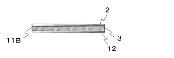
- 5 and 6 are schematic diagrams for explaining the discharge mode.
- FIG. 5 shows a glow discharge 11B
- FIG. 6 shows a streamer discharge 11A.
- the plasma becomes non-uniform and unstable, making it difficult to form a uniform thin film, and high temperature due to concentrated discharge, and plastic substrates that require low-temperature plasma treatment are thermally damaged. There was a problem that.
- the inventors of the present invention cover the opposing surface of the opposing electrode 2 to which a voltage is applied with the solid dielectric 3 and the distance between the opposing electrodes 2 and 12 is narrow (for example, the distance between the opposing electrodes 2 and 12 is 1 mm, the frequency is 20 kHz.
- a positive / negative pulse voltage with a peak width of 7 kV, a discharge gas He, and an apparatus internal pressure of 1 atm, a glow-like discharge (glow discharge) 11B is generated in which the creeping discharge on the dielectric surface reaches the ground electrode as shown in FIG.
- this electrode interval is widened, as shown in FIG.
- near-uniform discharge such as glow discharge is maintained in the vicinity (within 0.5 mm) from the opposing surface of the electrode 2 to which voltage is applied, and this uniform discharge is maintained. It has been found that a streamer discharge 11A is generated toward the surface of a base material having a surface resistance value in a specific range set on the opposing surface of the electrode 12 grounded from a near discharge region. About 2 to 10 streamer discharges are generated per 1 cm 2 , and the discharge form is also called filament discharge.
- the surface resistance of the substrate was required to be 10 3 ohm / sq or less.
- the surface resistance of the substrate 4 gives a conductive compound to the surface of the substrate 4 or in the substrate 4. It is preferable to adjust by mixing a conductive compound.
- the conductive compound is, for example, a metal such as carbon black, silver or copper, or a metal compound such as tin oxide or indium oxide.
- a plastic sheet such as a polyethylene terephthalate (PET) sheet or a polypropylene sheet
- the surface resistance is adjusted within the range of 1 to 1000 ohm / sq depending on the amount of carbon black added
- a boron-doped silicon wafer (thickness 0.4 mm, surface resistance 50 to 260 ohm / sq)
- a streamer discharge was also generated without any problem in a metal sheet as a conductor (steel plate, aluminum, titanium, etc., having a surface resistance of about 10 ⁇ 8 ohm / sq at a thickness of 0.3 mm).
- the surface resistance is a value measured according to JIS C 2139: 2008 “Solid Electrical Insulating Material—Measurement Method of Volume Resistivity and Surface Resistivity”.
- a polymer material having high surface resistance and high transparency may be used, and the polymer material may be covered with a film of a transparent conductive compound.
- a film of the transparent conductive compound for example, indium oxide / tin (ITO) film or PEDOT / PSS (poly (3,4-ethylenedioxythiophene) / poly (4-styrenesulfonic acid)) particles are used as a binder resin.
- ITO indium oxide / tin
- PEDOT / PSS poly (3,4-ethylenedioxythiophene) / poly (4-styrenesulfonic acid) particles are used as a binder resin.
- a dispersed film may be mentioned.
- a commercially available product may be used as the base material.
- Lion's LeoPound PET M3000 (thickness 0.15 mm, surface resistance 49.8 ohm / sq) is commercially available as a master batch pellet in which about 10% of carbon black is kneaded into PET.
- a PET sheet having a predetermined surface resistance can be obtained by dispersing the master batch pellet in the PET pellet at a certain ratio.
- the voltage applied by the power source may be a pulsed voltage having a high frequency or a rest period.
- the high frequency and the pulse voltage preferably have an alternating waveform.
- the voltage between the positive peak and the negative peak is preferably in the range of 2 to 10 times the discharge start voltage determined by the distance between the counter electrodes 2 and 12, the discharge gas type and the pressure.
- a streamer discharge suitable for forming a high-quality thin film is generated by applying a voltage in the range of 2 to 10 times the discharge start voltage under atmospheric pressure or a pressure condition near atmospheric pressure.
- the “pressure condition near atmospheric pressure” includes a pressure near atmospheric pressure, and specifically refers to an absolute pressure under a pressure in the range of, for example, 80 to 120 kPa.
- the distance between the counter electrodes should be in the range of 3 mm to 20 mm. Is preferred. If it is less than 3 mm, the influence of creeping discharge on the dielectric surface and the discharge distance are short, so that the growth of streamer discharge is suppressed and the electron density and ion density cannot be increased.
- the distance between the counter electrodes is more preferably 4 mm or more and 15 mm or less. By setting it as this range, while being able to generate streamer discharge more reliably, the damage to a board
- the distance between the opposing electrodes is the distance between the opposing surfaces of the opposing electrodes 2 and 12, and is the distance d at the portion where the opposing surfaces are closest to each other. .
- the frequency of the alternating high frequency and the pulsed voltage is in the range of 1 to 100 kHz, and the converted electric field is in the range of 30 to 1000 Td. .
- the counter electrodes 2 and 12 are arranged to face each other in a parallel plate shape, the case where at least one of the counter electrodes has a prismatic shape is included.
- FIG. 4 shows an example in which one electrode 2 has a prismatic shape and the other electrode 12 has a flat plate shape.
- the prismatic shape of the electrode 2 has a depth that matches the width of the other electrode 12 in the depth direction (the normal direction of the plane of FIG. 4). In FIG. By moving either one of them in the horizontal direction (the left-right direction of the paper surface shown in FIG. 4), it is possible to continuously form a film in a large area.
- the tip of the streamer discharge 11A reaches the surface of the substrate 4 having a low surface resistance, and ions derived from the reaction gas collide with the surface of the substrate 4.
- the thin film 10 is formed by diffusing on the surface of the substrate 4 and bonding to each other.
- the power density is about 10 times that of the glow discharge, the ion density and the electron density are both kept about 1000 times higher, and the recombination in the streamer is also less, so the vacuum method is used.
- the surface resistance increases, so that the electric field density in the streamer discharge gradually decreases.
- the power density in the plasma also decreases, and the thickness of the thin film 10 formed accordingly increases in uniformity and density.
- the thin film 10 becomes the inclination structure from which a grain boundary becomes indefinite as it goes to the outer surface.
- the thin film according to the present embodiment has high adhesion to the base material due to the inclined structure in which the crystal structure changes in the thickness direction of the thin film, and has a function equal to or higher than that of the thin film formed by the vacuum method. It can be demonstrated.
- the thin film forming method according to the present embodiment forms a thin film having high functionality (high hardness, scratch resistance, etc.) equivalent to the vacuum method under atmospheric pressure on the substrate by utilizing streamer discharge. It is possible. Moreover, the temperature at the time of forming a thin film can be low (room temperature to about 100 ° C.), and can be applied to a plastic substrate. Moreover, since atmospheric pressure CVD is used, apparatus cost and operation cost are low compared with the conventional vacuum process. Furthermore, since the film formation rate is faster than that of the vacuum process, it can be expected that the manufacturing cost will be significantly reduced.
- the film was formed by changing the distance between the counter electrodes 2 and 12.
- the distance d between the opposing electrodes 2 and 12 is 1 mm, and a silicon substrate (surface resistance 263 ohm / sq, thickness 0.38 mm) is disposed on the opposing surface of the electrode 12 as the substrate 4 under a pressure of 100 kPa.
- a mixed gas containing 200 mL / min of methane (CH 4 ) as a reaction gas and 4 L / min of helium (He) and 1 L / min of argon (Ar) as a discharge gas is supplied from a gas supply path, and has a frequency of 30 kHz.
- a pulse voltage was applied under a power supply condition of a pulse width of 5 ⁇ s and a voltage of 10 kV to generate a discharge, and a thin film having a thickness of 500 nm was formed on the surface of the substrate 4.
- the film thickness was measured using a stylus type surface shape measuring instrument (Dektak 3030, manufactured by Veeco Instruments Inc., USA).
- Example 1 Discharge Form The discharge form at the time of preparing the specimens 1 to 4 was observed.
- the discharge form of the specimens 1 to 4 is shown in FIG.
- the specimen 1 (distance between opposing electrodes 1 mm) was glow discharge.
- the specimen 2 (distance between the opposing electrodes 2 mm)
- glow discharge and streamer discharge were mixed.
- Specimens 3 and 4 (distance between opposing electrodes 3 and 4 mm) were streamer discharges throughout. From the above, it was confirmed that streamer discharge was generated by setting the distance between the counter electrodes to 3 mm or more.
- FIG. 8 shows an image in which the discharge mode is processed in gray tone, but the discharge mode is more accurately represented by a color image before processing in gray tone.
- Example 2 Film formation rate The relationship between the distance between counter electrodes and the film formation rate was confirmed.
- Five specimens 1 to 4 were prepared. In making each specimen, the time (film formation time) required to form a thin film having a thickness of 500 nm was measured.
- the film formation rate (unit: s) was obtained by dividing the film thickness (unit: nm) by the average value (unit: s) of the film formation time. nm / s).
- FIG. 9 shows the relationship between the distance between the counter electrodes and the film formation rate.
- the film formation rate increased rapidly by setting the distance between the counter electrodes to 3 mm or more. This is presumably because the streamer discharge has a higher ion density inside the streamer than the glow discharge, and thus the decomposition of the reaction gas is further promoted.
- the fluorescence caused by the polymer structure was reduced by setting the distance between the counter electrodes to 3 mm or more. This is presumably because the streamer discharge has a higher ion density inside the streamer than the glow discharge, and thus the reaction between ions is further promoted.
- FIG. 11 shows the relationship between the distance between the counter electrodes and N / (N + S).
- N / (N + S) was rapidly decreased by setting the distance between the counter electrodes to 3 mm or more. From this, it can be inferred that the thin film formed by streamer discharge has a lower hydrogen concentration in the thin film than the thin film formed by glow discharge. This is presumably because the streamer discharge has a higher ion density inside the streamer than the glow discharge, so that the reaction of ions is more activated and hydrogen is extracted.
- Example 4 IR Analysis For Specimens 1 to 4, the thin film was analyzed by the FTIR (Fourier Transform Infrared Spectroscopy) method, and the relationship between the distance between the counter electrodes and the sp 3 -CHx peak was confirmed. FTIR spectra of specimens 1 to 4 are shown in FIG. The FTIR analysis was performed using an infrared spectrometer (ALPHA-T, Bruker Corp., USA).
- APHA-T infrared spectrometer
- Example 5 Surface Roughness
- the surface roughness of the thin film was measured with a scanning probe microscope (“SPM-9700”, manufactured by Shimadzu Corporation) using JIS R 1683: 2007 “Atomic force. The measurement was performed in accordance with “Measurement method of surface roughness of fine ceramic thin film by microscope”. The surface roughness was 0.41 nm for Specimen 1, 0.29 nm for Specimen 2, 0.19 nm for Specimen 3, and 0.25 nm for Specimen 4.
- Example 6 Hardness The specimens 1 to 4 were evaluated for the hardness of the thin film.
- FIG. 13 shows the relationship between the distance between the counter electrodes and the indentation depth. Moreover, the relationship between the distance between counter electrodes and indentation hardness is shown in FIG. The hardness was measured by performing a nanoindentation test using a Barcovic indenter according to ISO 14577-2002 using a nanoindenter system (“Nano Indenter G200” manufactured by Agilent Technologies), and measuring the indentation depth. Indentation hardness was calculated.
- the indentation depth tends to decrease.
- the indentation hardness (Hardness) calculated using the indentation depth value tended to increase as the distance between the counter electrodes increased.
- the indentation hardness was substantially constant when the distance between the counter electrodes was 3 mm or more. This is thought to be because the streamer discharge has a higher ion density inside the streamer than the glow discharge, so that the reaction of ions becomes more active and hydrogen is extracted, resulting in a lower hydrogen concentration in the thin film. .
- a mixed gas containing 200 mL / min of methane (CH 4 ) as a reaction gas, 4 L / min of helium (He) and 1 L / min of argon (Ar) as a discharge gas under a pressure of 100 kPa was supplied from the gas supply path, and a pulsed voltage was applied under the power supply conditions of a frequency of 20 kHz, a pulse width of 5 ⁇ s, and a voltage of 7 kV to generate a discharge to form a thin film having a thickness of 280 nm on the surface of the substrate 4. .
- the film formation time was 120 s.
- the discharge form of the specimen 5 was glow discharge.
- Specimen 5 is a comparative example, and specimens 6 to 8 are products of the present invention.
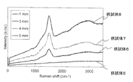
- FIG. 15 shows Raman spectra of specimens 5 to 8.
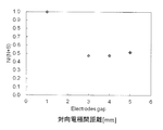
- FIG. 16 shows the relationship between the distance between the counter electrodes and N / (N + S). As shown in FIG. 15, G-band could not be confirmed when the distance between the electrodes was 1 mm, but it was confirmed that the distance between the electrodes was 3 mm or more. As shown in FIG. 16, N / (N + S) was rapidly decreased by setting the distance between the electrodes to 3 mm or more. As described above, it was confirmed that the film can be formed satisfactorily even when a metal base material is used by generating streamer discharge.
- a surface resistance of 10 3 ohm / sq) is arranged on the opposite surface of the electrode 12 with the SnO 2 coating surface facing upward, and under a pressure of 100 kPa, methane (CH 4 ) 200 mL / min as a reaction gas, and a discharge gas
- methane (CH 4 ) 200 mL / min as a reaction gas
- a discharge gas A mixed gas containing helium (He) 4 L / min and argon (Ar) 1 L / min is supplied from the gas supply path, and a pulse voltage is applied under power supply conditions of a frequency of 30 kHz, a pulse width of 5 ⁇ s, and a voltage of 11 kV. Then, a discharge was generated to form a thin film having a film thickness of 60 nm on the surface of the substrate 4.
- the film formation time was 25 s.
- Specimens 9 to 11 are products of the present invention, and specimen 12 is a comparative example.
- FIG. 17 shows Raman spectra of the specimens 9 to 12.
- FIG. 18 shows the relationship between the film formation time and N / (N + S).
- the specimen 12 could not be formed because an insulating SiO 2 substrate was used, but the specimens 9 to 11 were formed by coating conductive SnO 2 on the insulating SiO 2 substrate. A thin film having G-band could be formed. From this, it was confirmed that the film could be formed regardless of the material of the substrate by adjusting the surface resistance within a predetermined range.
- N / (N + S) was about 0.7 to 0.8.
- specimens 9 to 11 were slightly higher.
- the distance d between the counter electrodes 2 and 12 is 2 mm, and a silicon substrate (surface resistance 263 ohm / sq, thickness 0.38 mm) is opposed to the electrode 12 as the substrate 4.
- TrMS trimethylsilane
- oxygen O 2
- N 2 nitrogen
- a pulsed voltage is applied under the power supply conditions of a frequency of 30 kHz, a pulse width of 5 ⁇ s and a voltage of 18 kV to generate a discharge to form a SiOx thin film on the surface of the substrate 4 did.
- the discharge form was streamer discharge.
- Specimen 13 is the product of the present invention. It was confirmed that the thin film forming method according to the present invention can form a film satisfactorily regardless of the type of the reaction gas.
- the distance d between the counter electrodes 2 and 12 is 3 mm, and a silicon substrate (surface resistance 263 ohm / sq, thickness 0.38 mm) is opposed to the electrode 12 as the substrate 4. It is arranged on the surface, and under a pressure of 100 kPa, methane (CH 4 ) 400 mL / min as a reaction gas and helium (He) 5 L / min as a discharge gas are supplied from a gas supply path, with a frequency of 30 kHz and a pulse width. A pulsed voltage was applied under power supply conditions of 5 ⁇ s and a voltage of 7 kV to generate a discharge, and a thin film having a thickness of 240 nm was formed on the surface of the substrate 4. The film formation time was 100 s.
- Example 10 The indentation hardness of the thin films formed on the specimens 14 to 19 was measured and the surface state was observed.
- the results are shown in Table 1.
- the composition of the discharge gas preferably includes helium in the range of 40 to 100%, argon in the range of 60 to 0%, and helium in the range of 60 to 100% as the volume ratio in the standard state. It was confirmed that it was more preferable to include in the range, and to include argon in the range of 40 to 0%.
- the thin film has an inclined structure in which the grain boundary density decreases continuously or intermittently from the inner surface of the thin film toward the outer surface of the thin film,
- a thin film characterized in that the innermost region in contact with the surface of the substrate of the thin film has a grain boundary structure in which the grain boundary has a particle size of 10 to 30 nm.
- a pair of counter electrodes composed of a first electrode connected to a power source for applying a voltage and a grounded second electrode; and a gas supply path for supplying a mixed gas containing a reaction gas and a discharge gas between the pair of counter electrodes
- a gas supply path for supplying a mixed gas containing a reaction gas and a discharge gas between the pair of counter electrodes
- Appendix 3 The thin film forming method according to appendix 2, wherein the opposing surface of the second electrode is covered with a solid dielectric.
- Appendix 4 The thin film forming method according to appendix 2 or 3, wherein the voltage applied by the power source is a pulsed voltage having a high frequency or a rest period.
- the high-frequency or pulse-like voltage has an alternating waveform, and the voltage between the positive peak and the negative peak is a discharge start voltage determined by the distance between the counter electrodes, the discharge gas type, and the pressure. 5.
- Appendix 6 The method of forming a thin film according to appendix 4 or 5, wherein the frequency of the alternating high frequency or pulse voltage is in the range of 1 to 100 kHz, and the converted electric field is in the range of 30 to 1000 Td.
- Appendix 7 The method of forming a thin film according to any one of appendices 2 to 6, wherein the distance between the closest facing surfaces between the opposing electrodes is 3 to 20 mm.
- the counter electrode is disposed so as to be opposed to a flat plate shape, or at least one of the electrodes has a cylindrical, prismatic, cylindrical, or spherical shape, according to any one of appendices 2 to 7, Thin film forming method.
- the reactive gas is a compound containing carbon, hydrogen and / or oxygen when forming a carbon-based thin film, or an organometallic compound and oxygen when forming a metal oxide thin film.
- the thin film forming method according to any one of 1 to 8.
- Appendix 10 The thin film forming method according to appendix 9, wherein when forming the carbon-based thin film, any one of methane, ethane, and propane or a mixture thereof is used as a reaction gas.
- the discharge gas is composed of helium or helium and argon, and the composition of the discharge gas includes helium in a range of 40 to 100% as a standard volume ratio, and argon in a range of 60 to 0%.
- Electrode (1st electrode) 3 Solid Dielectric 4 Base Material 5 Gas Supply Path 6 Mixed Gas 7 Plasmaized Mixed Gas 8 Exhaust Path 10 Thin Film 11A Streamer Discharge 11B Glow Discharge 12 Electrode (Second Electrode)
Landscapes
- Chemical & Material Sciences (AREA)
- Engineering & Computer Science (AREA)
- Plasma & Fusion (AREA)
- Physics & Mathematics (AREA)
- Chemical Kinetics & Catalysis (AREA)
- General Chemical & Material Sciences (AREA)
- Spectroscopy & Molecular Physics (AREA)
- Materials Engineering (AREA)
- Mechanical Engineering (AREA)
- Metallurgy (AREA)
- Organic Chemistry (AREA)
- Chemical Vapour Deposition (AREA)
- Plasma Technology (AREA)
Abstract
本開示は、上記の課題を解決し、基材表面に真空を利用したプラズマCVD法によって得られる薄膜と同等もしくはそれ以上の高機能性(硬度および耐摩耗性等)を有し、かつ基材との密着性の高い薄膜およびその薄膜形成方法を提供することを目的とする。本発明に係る薄膜は、基材の表面に設けられた薄膜において、該薄膜は、薄膜の内表面から薄膜の外表面に向かうにつれて粒界密度が連続的または断続的に小さくなる傾斜構造を有し、前記薄膜の前記基材の表面に接する最内部領域は、粒界の粒径が10~30nmである粒界構造を有する。
Description
本開示は、基材の表面に形成された薄膜およびその薄膜の形成方法に関する。さらに詳しくは、基材との密着性が高い傾斜構造を有する、炭素薄膜もしくは金属酸化物薄膜などの薄膜、ならびに該薄膜を大気圧もしくは大気圧近傍の圧力下(以降、大気圧下ということもある。)で発生させた放電プラズマを利用して、基材表面に薄膜を形成する方法に関する。
高分子または金属材料などの基材の表面に薄膜を形成することによって、低コストかつ省資源で簡便に、バルクとしての基材に高機能性(例えば、高硬度、耐スクラッチ性または高ガスバリア性等)を付与する技術が従来から広く実用に供されている。近年では、酸化ケイ素または酸化アルミニウムなどの金属酸化物からなる無機薄膜を、プラスチック基材または金属基材表面にコーティングする技術が開発され、表面保護、ガスバリア性または美粧性などの機能を付与する技術が普及している(例えば、特許文献1を参照。)。
また、金属酸化物に代えて非晶質の炭素系薄膜(DLC:ダイヤモンドライクカーボン)をコーティングする技術も開示されている(例えば、特許文献2を参照。)。
これらの無機薄膜は、従来真空下でのスパッタリング、イオンプレーティングもしくは真空蒸着法などの物理気相蒸着法、または高周波もしくはマイクロ波によって励起したプラズマによって化学種を活性化して化学反応蒸着するプラズマCVD(Chemical Vapor Deposition)法によって成膜する方法が一般的である。いずれも高真空から中真空の低圧領域での成膜が必須となっている。低圧領域での成膜では、膜の原料となる活性種が気相中で他分子または活性種同士で衝突することが少ないため、形成された無機薄膜は均一な非晶質膜であることが特徴である。しかし一方では、形成した薄膜が厚さ方向にも均一であるため、例えば、高硬度、耐摩耗性または高ガスバリア性などの機能を有する薄膜では、基材との界面において基材との特性の差異が大きすぎて剥離を生じる場合があり、密着性に問題があった。
このため薄膜を積層構造にして密着性を維持しながら薄膜表面では高い機能を維持する積層膜が各種提案されている(例えば、特許文献3および特許文献4を参照。)。
さらに製造面では、低圧領域での成膜に用いる成膜装置は、真空を維持するためのチャンバーおよび真空ポンプなどの設備コストがかかり、その運転経費および取り扱いも容易ではない問題があった。これら真空プロセスに起因する問題を解決するため大気圧下において無機薄膜を成膜する大気圧プラズマCVD法も提案されている(例えば、特許文献5および特許文献6を参照。)。特許文献5および特許文献6では、高電圧のパルス電源を使用し、大気圧下で誘電体バリア放電によってダイヤモンド状炭素薄膜を製造する方法を開示している。一般的に、誘電体バリア放電による大気圧プラズマCVD法では、グロー放電が利用される(例えば、非特許文献1を参照。)
「大気圧プラズマの生成制御と応用技術」、小駒 益弘(監修)、福嶋 邦彦(発行者)、サイエンス&テクノロジー株式会社、2006年11月29日 初版第1刷、p23-33
三浦健一、中村守正、表面技術、59、(2008)203
しかし特許文献3または特許文献4のように、薄膜の積層構造によって基材との密着性を高める方法は、組成および構造の異なる薄膜を複数形成する必要があるため製造にあたって装置が複雑化し、また製造に要するコストも大きいという問題があった。
特許文献5または特許文献6のように、誘電体バリア放電を利用する方式は、非特許文献1に示されるように、大気圧グロー放電を維持して低温で均一なプラズマ状態を得るため電界強度が低く、ガス密度が高いにもかかわらず高密度なプラズマを発生させることができない。このため、真空法(真空を利用したプラズマCVD法)に比べて形成した薄膜の密度、硬度およびガスバリア性などの機能が低いという問題があった。また、大気圧もしくは大気圧近傍の圧力下での成膜では、活性種が気相中で他分子または活性種同士で衝突することが多いため、真空法によって得られた薄膜と異なり粒子が互いに接着して形成された粒界を有する不均一な構造となっている。さらに、気相中での相互衝突に運動エネルギーが低下するため基材への衝突エネルギーも真空法に比べて小さく、その結果基材との密着性もより低くなる。大気圧下において高密度プラズマを得るために電界強度を高くすると、電離が急激に派生する。その結果電子なだれが線状に成長し、ストリーマ放電が発生する。ストリーマ放電が発生すると、プラズマが不均一になり、さらに熱電子の発生にともなってアーク放電に移行して高温プラズマとなるため基材の損傷が大きくなり、薄膜の形成は困難である。このため、従来、大気圧プラズマCVD法では、ストリーマ放電の発生を抑制することが好ましいとされてきた。
本開示は、上記の課題を解決し、基材表面に真空を利用したプラズマCVD法によって得られる薄膜と同等もしくはそれ以上の高機能性(硬度および耐摩耗性等)を有し、かつ基材との密着性の高い薄膜およびその薄膜形成方法を提供することを目的とする。
前記の通り、従来、誘電体バリア放電による大気圧プラズマCVD法では、ストリーマ放電の発生を抑制することが好ましいとされてきた。しかし、本発明者らは、誘電体バリア放電による大気圧プラズマCVD法において、ストリーマ放電を利用して、高機能性を有する薄膜を形成できることを見出し、本発明を完成するに至った。すなわち、本発明に係る薄膜は、基材の表面に設けられた薄膜において、該薄膜は、該薄膜の内表面から該薄膜の外表面に向かうにつれて粒界密度が連続的または断続的に小さくなる傾斜構造を有し、前記薄膜の前記基材の表面に接する最内部領域は、粒界の粒径が10~30nmである粒界構造を有することを特徴とする。
本発明に係る薄膜形成方法は、電圧を印加する電源に接続された第1電極および接地された第2電極からなる一対の対向電極と、該一対の対向電極間に反応ガスおよび放電ガスを含む混合ガスを供給するガス供給路と、を備え、前記第1電極の対向面は固体誘電体によって覆われている成膜装置を用いた薄膜形成方法において、前記第2電極の対向面上に、表面抵抗が10-8~103オーム/sqの範囲の基材を設置する工程と、大気圧または大気圧近傍の圧力下で、前記一対の対向電極間に前記ガス供給路から前記混合ガスを供給するとともに前記電源によって電圧を印加してストリーマ放電を発生させてプラズマCVDで前記基材の表面に薄膜を形成する工程と、を有することを特徴とする。
本発明に係る薄膜形成方法では、前記放電ガスは、ヘリウム、アルゴン、窒素の少なくとも1種もしくはこれらの混合物であることが好ましい。
本発明に係る薄膜形成方法では、前記放電ガスは、ヘリウムからなるか、又はヘリウムとアルゴンとからなり、前記放電ガスの組成は、標準状態の体積比率としてヘリウムを40~100%の範囲で含み、アルゴンを60~0%の範囲で含むことが好ましい。
本開示によれば、基材表面に真空を利用したプラズマCVD法によって得られる薄膜と同等もしくはそれ以上の高機能性(硬度および耐摩耗性等)を有し、かつ基材との密着性の高い薄膜およびその薄膜形成方法を提供することができる。
以下、本発明の実施形態について、図面を参照しながら詳細に説明する。なお、本発明は、以下に示す実施形態に限定されるものではない。これらの実施の例は例示に過ぎず、本発明は当業者の知識に基づいて種々の変更、改良を施した形態で実施することができる。なお、本明細書及び図面において符号が同じ構成要素は、相互に同一のものを示すものとする。
図1は、本実施形態に係る薄膜断面の走査式電子顕微鏡画像である。本実施形態に係る薄膜は、図1に示すように、基材の表面に設けられた薄膜において、該薄膜は、薄膜の内表面から薄膜の外表面に向かうにつれて粒界密度が連続的または断続的に小さくなる傾斜構造を有し、前記薄膜の前記基材の表面に接する最内部領域は、粒界の粒径が10~30nmである粒界構造を有する。
薄膜の種類は、特に限定されないが、例えば、炭素系薄膜、金属酸化物薄膜または珪素系薄膜である。薄膜の厚さは、100~800nmであることが好ましく、200~600nmであることがより好ましい。
本明細書において、最内部領域は、薄膜を外表面から見た最深部のことであり、薄膜の内表面(薄膜の基材と接する側の表面)を含む。最内部領域は、薄膜の厚さ方向において、薄膜の内表面から薄膜の外表面(薄膜の基材と接する側とは反対側の表面)へ向かう方向に30nmまでの領域を含むことが好ましい。また、最外部領域は、薄膜を外表面から見た最浅部のことであり、薄膜の外表面を含む。最外部領域は、薄膜の厚さ方向において、薄膜の外表面から基材へ向かう方向に30nmまでの領域を含むことが好ましい。また、薄膜の断面を倍率40000倍で観察した走査式電子顕微鏡(SEM)または透過型電子顕微鏡(TEM)の画像において、粒界が観察される場合を粒界構造と判断し、粒界が観察されない場合を非晶質構造と判断する。
図1に示す薄膜は、例えば、図4に示す成膜装置で成膜することができる。互いに平行に配置された例えば銅製の対向電極2、12のうち、対向電極2の対向面側には、固体誘電体3が配置されている。固体誘電体3としては、例えば、ポリテトラフルオロエチレン、ポリエチレンテレフタレートもしくはポリエチレンなどのプラスチック、ガラス、またはアルミナなどの金属酸化物が使用できる。固体誘電体3と他方の対向電極12との間に、基材4が配置される。
対向電極2、12間には、ガス供給路5を通して、反応ガス成分を含有する混合ガス6が、所定の流速で対向電極2、12の隙間に供給される。混合ガス6は、対向電極2、12間に印加される高周波電圧によってプラズマ化され、プラズマ化混合ガス7となる。プラズマ化混合ガス7に含有される反応ガス成分の一部は、基材4の表面に堆積し、薄膜(不図示)を形成する。対向電極2、12間を通過し、反応ガス成分の一部が消費された混合ガス6は、排気路8を通して系外に排出される。
図1の薄膜は、ストリーマ放電を利用した大気圧プラズマCVD法(以降、「大気圧法(ストリーマ放電)」ということもある。)で成膜した薄膜である。図1に示す薄膜は次の通り形成した。すなわち、対向電極2,12間の距離dを4mmとし、基材4としてシリコン基材(表面抵抗260オーム/sq、厚さ0.38mm)を電極12の対向面上に配置し、100kPaの圧力下で、反応ガスとしてメタン(CH4)400mL/minと、放電ガスとしてヘリウム(He)4L/minおよびアルゴン(Ar)1L/minとを含む混合ガスを、ガス供給路から供給するとともに、周波数30kHz、パルス幅5μsおよび電圧7kVの電源条件でパルス状電圧を印加して、放電を発生させて基材4の表面に膜厚500nmの薄膜を形成した。成膜時間は250sであった。成膜装置1において、対向電極2,12は銅製とした。
図1に示すように、大気圧法(ストリーマ放電)で成膜した薄膜の構造は、基材の表面に接する最内部領域では粒界が明確に形成される粒界構造を有していた。最内部領域における粒界の粒径は10~30nmの範囲であった。ここで、粒界の粒径は、SEMまたはTEMによる断面観察で倍率40000倍のときに粒界構造を濃淡によって確認できた場合に、一体となっている粒界構造の外縁の縦の直径と横の直径の平均値として求めたものである。薄膜は、該薄膜の最外部領域に近づくにつれて傾斜的に粒界が不明確となって均一の非晶質構造に近づいていく構造を示していた。
本実施形態に係る薄膜は、薄膜の内表面から薄膜の外表面に向かうにつれて粒界密度が連続的または断続的に小さくなる傾斜構造を有する。粒界密度(無次元数)とは、SEMまたはTEMにおける断面観察の倍率40000倍において、濃淡によって確認できた粒界構造と、粒界構造の間の連続的非晶質部分との単位面積当たりの面積比である。
図1では、薄膜の厚さ方向において、薄膜の内表面から薄膜の外表面(薄膜の基材と接する側とは反対側の表面)へ向かう方向に30nmまでの領域(最内部領域)では、粒界の粒径が10~30nmの粒界構造を有していた。また、薄膜の厚さ方向において、薄膜の外表面から基材へ向かう方向に30nmまでの領域(最外部領域)では、非晶質構造であった。最内部領域と最外部領域との間の領域には、粒界構造を有する部分と非晶質構造を有する部分とが混在していた。最内部領域と最外部領域との間の領域を厚さ方向に二等分したとき、最内部領域側の領域では粒界構造を有する部分が非晶質構造を有する部分よりも多く見られたが、最外部領域側の領域では非晶質構造を有する部分が粒界構造を有する部分よりも多く見られた。また、粒界密度は、薄膜の内表面から薄膜の外表面に向かうにつれて小さくなる傾向が見られた。
図1では、薄膜の最外部領域が非晶質構造を有する形態を示したが、本実施形態では薄膜の最外部領域が粒界構造を有していてもよい。本実施形態では、最外部領域が粒界構造を有するとき、最外部領域における粒界の粒径は、最内部領域における粒界の粒径よりも大きいことが好ましい。最外部領域が粒界構造を有する薄膜は、たとえば、薄膜の形成において所定の膜厚となったところで停止することで得ることができる。所定の膜厚は、基材の種類、混合ガスの種類、ガス流量および成膜装置の電源条件など成膜条件によって異なるが、たとえば図1の薄膜の形成条件では、100~250nmである。
次に、本実施形態に係る薄膜と従来の薄膜との断面構造を比較する。
図2は、真空プラズマCVD法(以降、「真空法」ということもある。)で成膜した薄膜断面の走査式電子顕微鏡画像である。図2に示す薄膜は次の通り形成した。すなわち、平行平板法による高周波プラズマCVD装置を用い、0.1Torr(13.3Pa)の圧力下で、反応ガスとしてアセチレン(C2H2)を用い、高周波電力200W、周波数13.56MHzの条件で成膜を行った。薄膜の膜厚は500nmであり、成膜時間は100sであった。
図3は、グロー放電を利用した大気圧プラズマCVD法(以降、「大気圧法(グロー放電)」ということもある。)で成膜した薄膜断面の走査式電子顕微鏡画像である。図3に示す薄膜は次の通り形成した。すなわち、図1の薄膜の作製において、対抗電極間の距離を1mmとし、反応ガスとしてアセチレン(C2H2)20mL/minと放電ガスとして窒素(N2)1L/minとを含む混合ガスを用い、電源条件を周波数10kHz、パルス幅5μsおよび電圧18kVに変更した以外は、図1の薄膜と同様にして作製した。薄膜の膜厚は800nmであり、成膜時間は50sであった。
図1~図3は、倍率40000倍で観察した像である。
図2に示すように、真空法で成膜した薄膜の構造は、該薄膜の厚さ方向の全体にわたって均一な非晶質を有しており、粒界を形成する構造を示さなかった。また、図3に示すように、大気圧法(グロー放電)で成膜した薄膜の構造は、該薄膜の厚さ方向の全体にわたって粒界の粒径が50~100nmである明確な粒界構造を示していた。
また薄膜の硬度は、大気圧法(ストリーマ放電)では12GPa、大気圧法(グロー放電)では3GPa、真空法では12GPaであった。硬度は、ナノインデンター・システム(「Nano Indenter G200」 Agilent Technologies社製)を用いてISO 14577-2002に準拠してバーコビッチ圧子を使用してナノインデンテーション試験を行い、押し込み深さを測定し、押し込み硬度を算出した。薄膜の耐剥離性は、クロスカット剥離試験(JIS K 5600-5-6:1999「塗料一般試験方法-第5部:塗膜の機械的性質-第6節:付着性(クロスカット法)」)によれば、良好な方から順に、大気圧法(ストリーマ放電)、真空法、大気圧法(グロー放電)であった。この結果から、基材と薄膜との界面では粒径が10~30nm程度の粒界構造の方が、粒界のない均一な非晶質構造よりも密着性が高いことがわかる。また、粒径が50nm以上になると気相中で運動エネルギーを失うため基材との密着性が、粒径が10~30nmの場合と比較して低下することがわかる。一方、図1および図2の薄膜のように薄膜の最外部領域が非晶質構造となっていることによって、高い硬度特性を示すことが確認できた。以上より、大気圧法(ストリーマ放電)によって成膜した薄膜は傾斜構造を有することによって、真空法によって得られる薄膜と同等もしくはそれ以上の、高硬度特性および高密着特性を有していることが認められた。
薄膜の表面粗さについて、大気圧法(ストリーマ放電)と大気圧法(グロー放電)とを比較すると、大気圧法(ストリーマ放電)の方が、大気圧法(グロー放電)よりも表面粗さが小さかった。表面粗さは、走査型プローブ顕微鏡(「SPM-9700」、島津製作所社製)を用い、JIS R 1683:2007「原子間力顕微鏡によるファインセラミックス薄膜の表面粗さ測定方法」に準拠して測定した。
また耐磨耗性をテーバー式磨耗試験機によってJIS K 7204:1999「プラスチック―摩耗輪による摩耗試験方法」に準拠して評価すると、大気圧法(ストリーマ放電)で得た薄膜がもっとも耐磨耗性が高かった。次いで、真空法、大気圧法(グロー放電)の順であった。
本実施形態に係る薄膜は、薄膜の外表面に近づくにしたがって水素濃度が多くなる傾斜構造を有することが好ましい。最外部領域の水素濃度が最内部領域に比べて増加する傾斜的特性を有することによって、摺動性および緩衝性が増し、その結果、薄膜の耐磨耗性が向上する。
薄膜中の水素濃度は、たとえば、二次イオン質量分析法(Secondary Ion Mass Spectrometry、SIMS)によって、薄膜を深さ方向分析することで測定することができる。また、薄膜中の水素濃度は、ラマン分析結果から推測してもよい。ラマン分光法は物質に照射した光の散乱光(ラマン散乱光)を分光測定する分析法で、物質の組成および構造を解析できる。典型的なDLC膜のラマンスペクトルは1500cm-1付近のGバンドと1300cm-1付近のDバンドとで構成される。これらの強度比からグラファイトクラスター化度または間接的にsp3/sp2結合成分比を求めることができるが、水素濃度が高くなるとバックグラウンド(蛍光成分)強度が大きくなることが知られている。そこで、Gバンドのピーク位置におけるラマン散乱光強度をS、蛍光成分強度をNとしたとき、水素濃度定性分析値になり得るパラメーターとしてlog(N/S)またはN/(N+S)が定義される(例えば、非特許文献2を参照。)。
図1の薄膜の作製において、膜厚を1000nmとした以外は、図1の薄膜の作製と同様の方法で薄膜を形成した。このとき、膜厚200nm毎にラマン分析を行い、N/(N+S)を求めた。膜厚とN/(N+S)との関係を図14に示す。
図14に示すとおり、N/(N+S)は200nmでは0.5であり、800nmでは0.75であった。そして、800nmまでは、薄膜の外表面に近づくほどN/(N+S)が増加しており、800nm以上ではN/(N+S)は略一定であった。このことから、供試体5の薄膜は、薄膜の外表面に近づくにしたがって水素濃度が多くなる傾斜構造を有することが確認できた。
図2に示す大気圧法(グロー放電)で形成した薄膜は、N/(N+S)が0.9~1程度であり、水素濃度の傾斜は見られなかった。大気圧法(ストリーマ放電)では、大気法(グロー放電)よりも薄膜の外表面における水素濃度が低いことが確認できた。また、図3に示す真空法で形成した薄膜は、N/(N+S)が0.6~0.7程度であり、水素濃度の傾斜は見られなかった。このことから、大気圧法(ストリーマ放電)では、薄膜の外表面における水素濃度が真空法と同程度であることが確認できた。この結果は、耐摩耗性評価の結果に整合している。
さらに原料ガスをトリメチルシランと酸素の混合ガスとしてヘリウムで希釈してSiOx薄膜をシリコン基板上に成膜した場合、やはり大気圧法(ストリーマ放電)で得られたSiOx薄膜の耐磨耗性がもっとも高かった。この理由は、薄膜が表面に近いほど粒界が不明確となって均一な非晶質構造に近づくと同時に、最外部領域の水素濃度が最内部領域に比べて増加し、密度がそれに伴って低下する傾斜的特性を有することによって、摺動性および緩衝性が増し、その結果耐磨耗性が増加したものと考えられる。
次に、図4を用いて本実施形態に係る薄膜形成方法を説明する。本発明は、図4に示す成膜装置に限定されるものではない。本実施形態に係る薄膜形成方法は、電圧を印加する電源に接続された第1電極2および接地された第2電極12からなる一対の対向電極2,12と、一対の対向電極2,12間に反応ガスおよび放電ガスを含む混合ガスを供給するガス供給路5と、を備え、第1電極2の対向面は固体誘電体3によって覆われている成膜装置1を用いた薄膜形成方法において、第2電極12の対向面上に、表面抵抗が10-8~103オーム/sqの範囲の基材4を設置する工程と、大気圧または大気圧近傍の圧力下で、一対の対向電極2,12間にガス供給路5から混合ガス6を供給するとともに電源によって電圧を印加してストリーマ放電を発生させてプラズマCVDで基材4の表面に薄膜を形成する工程と、を有する。
反応ガスは、薄膜の種類によって適宜選択され、本発明はこれに制限されない。炭素系薄膜を形成する場合、反応ガスは、例えば、炭素、水素および/または酸素を含有する化合物であり、メタン、エタンもしくはプロパンのいずれか一種またはこれらの混合物であることが好ましい。金属酸化物薄膜を形成する場合、反応ガスは、例えば、有機金属化合物および酸素である。有機金属化合物は、例えば、トリメチルアルミニウムまたはチタンテトライソポロポキシドである。珪素系薄膜を形成する場合、反応ガスは、例えば、有機珪素化合物および酸素である。有機珪素化合物は、例えば、トリメチルシラン(TrMS)、テトラエトキシシラン(TEOS)、テトラメトキシシラン(TMOS)またはヘキサメチルジシロキサン(HMDSO)である。各種薄膜の形成において、反応ガスは一種を単独で用いるか、または二種以上を混合して用いてもよい。
放電ガスは、ヘリウム、アルゴンもしくは窒素の少なくとも1種またはこれらの混合物を使用することが好ましく、とくにヘリウムを標準状態の体積%で40%以上、より好ましくは60%以上含むことが好ましい。また、放電ガスは、ヘリウムからなるか、又はヘリウムとアルゴンとからなり、放電ガスの組成は、標準状態の体積比率としてヘリウムを40~100%の範囲で含み、アルゴンを60~0%の範囲で含むことが好ましい。
図4に示すように、対向電極のうち一方の電極(図4では上部の電極)2は、好ましくは高周波電圧もしくはパルス電圧が印加され、他方の電極(図4では下部電極)12は接地されている。薄膜の原料となる反応ガスおよび電離して放電プラズマを発生させる放電ガスを含む混合ガス6が対向する電極の間に供給される。電圧が印加される対向電極2の対向面はアルミナなどの固体誘電体3で覆われる。放電開始した場合に固体誘電体3の表面への電荷蓄積によって放電電圧が低下する。このため、固体誘電体3は、固体誘電体3で覆われた電極2がカソード側になった場合にストリーマ放電が固体誘電体3の表面に連続して生じることが抑制され、また放電がアーク放電に移行することを防止する誘電体バリアとしての役割をする。図4では、対向電極2,12のうち、電圧が印加される電極2の対向面だけが固体誘電体3で覆われている形態を示したが、本実施形態では、電極2の対向面に加えて、接地された電極12の対向面も固体誘電体(不図示)で覆われていてもよい。
従来の大気圧プラズマを利用する薄膜形成方法では、たとえば非特許文献1に示されるように対向電極2,12間の距離をグロー放電が持続する距離に設定し、誘電体バリア放電(DBD)をグロー放電状態にして、反応ガスを活性化してプラズマCVD処理を行い、薄膜を形成していた。しかし大気圧プラズマを利用するグロー誘電体バリア放電(GDBD)では、プラズマ中の電子密度およびイオン密度が、真空法でのグロー放電に比べて高いものの、ガス分子の密度が高いため気相中で粒子生成または反応性を失う率が高く、基材表面での膜形成の速度はイオン密度に対して低く、形成された薄膜の密度も低い傾向にある。
本実施形態に係る薄膜形成方法では、グロー放電ではなく、ストリーマ放電を対向電極2,12の間に発生させ、基材の表面に薄膜を形成させる。図5および図6は、放電形態を説明するための模式図であり、図5はグロー放電11B、図6はストリーマ放電11Aを示す。従来ストリーマ放電が発生するとプラズマが不均一かつ不安定となるため均一な薄膜を形成することが困難であり、また集中した放電によって高温となり、低温プラズマ処理が必要なプラスチック基材では熱損傷を受けてしまうという問題があった。本発明者らは、電圧を印加する対向電極2の対向面を固体誘電体3で覆い、対向電極2,12間の距離が狭い条件(例えば、対向電極2,12間の距離1mm、周波数20kHzおよびピーク巾7kVの正負パルス電圧、放電ガスHe、装置内圧力1気圧)では、図5に示すように誘電体表面の沿面放電が接地電極に達するグロー状の放電(グロー放電)11Bが発生するが、この電極間隔を広くすると図6に示すように電圧を印加している電極2の対向面から近傍(0.5mm以内)ではグロー放電のような均一に近い放電が維持され、この均一に近い放電状領域から接地された電極12の対向面上に設置した特定の範囲の表面抵抗値を有する基材の表面に向けてストリーマ放電11Aが発生することを見出した。このストリーマ放電は、1cm2あたり2本から10本程度発生しており、フィラメント状放電とも呼ばれる放電形態であった。
このときストリーマ放電を発生させるためには、少なくとも基材の表面抵抗が103オーム/sq以下であることが必要であることがわかった。基材4が、表面抵抗が103オーム/sqを超える高分子材料からなるとき、基材4の表面抵抗は、基材4の表面に導電性化合物を付与するか、または基材4中に導電性化合物を混合して調整することが好ましい。導電性化合物は、たとえばカーボンブラック、銀もしくは銅などの金属、または酸化錫若しくは酸化インジウムなどの金属化合物である。たとえばポリエチレンテレフタレート(PET)シートもしくはポリプロピレンシートなどのプラスチックシート(厚さ0.1mm)に、カーボンブラックを練りこんで、カーボンブラック添加量によって表面抵抗1~1000オーム/sqの範囲に調整した場合、またはボロンドープシリコンウエファ(厚さ0.4mm、表面抵抗50~260オーム/sq)の場合にストリーマ放電が発生した。もちろん導電体である金属シート(鋼板、アルミニウム、チタン等、厚さ0.3mmにおいて表面抵抗10-8オーム/sq程度である)も問題なくストリーマ放電が発生した。本明細書において、表面抵抗とは、JIS C 2139:2008「固体電気絶縁材料-体積抵抗率及び表面抵抗率の測定方法」に準拠して測定した値である。
基材として表面抵抗が高く、かつ、透明性の高い高分子材料を用い、当該高分子材料を透明性の導電性化合物の膜で被覆してもよい。透明導電性化合物の膜としては、例えば、酸化インジウム/スズ(ITO)膜又はPEDOT/PSS(ポリ(3,4-エチレンジオキシチオフェン)/ポリ(4-スチレンスルフォン酸))粒子をバインダー樹脂に分散させた膜が挙げられる。
基材は市販品を用いてもよい。たとえば、PETにカーボンブラックを約10%練りこんだマスタバッチペレットとしてライオン社製のレオパウンドPET M3000(厚さ0.15mm、表面抵抗49.8オーム/sq)が市販されている。このマスタバッチペレットをPETペレットに一定比率で分散させることにより所定の表面抵抗のPETシートを得ることができる。
電源が印加する電圧は、高周波もしくは休止期間を有するパルス状の電圧であればよいが、印加する電極2の対向面が固体誘電体3に覆われているため、放電持続のためには、前記高周波およびパルス状電圧は、交流の波形を有していることが好ましい。また、その正ピークと負ピークとの間の電圧は、対向電極2,12間の距離、放電ガス種および圧力によって決定される放電開始電圧の2~10倍で範囲であることが好ましい。ストリーマ放電が生じ始める対向電極2,12間の距離の条件は、(1)式で表される(例えば、非特許文献1を参照。)。(1)式は、Meekの条件と呼ばれる。
(数1)αd=20 …(1)
(1)式において、dは、対向電極間の距離(mm)、αは電離係数である。
(数1)αd=20 …(1)
(1)式において、dは、対向電極間の距離(mm)、αは電離係数である。
発明者らの研究の結果、大気圧もしくは大気圧近傍の圧力条件下では、放電開始電圧の2~10倍で範囲の電圧を加えることによって、良質な薄膜の形成に適したストリーマ放電を発生させることができることがわかった。本明細書において、「大気圧近傍の圧力条件下」とは、大気圧近傍の圧力を含むものであり、具体的には絶対圧で例えば80~120kPaの範囲の圧力下をいう。対向電極間の距離dを拡大したり、印加電圧を放電開始電圧の2倍より少なくしたりすると、電極間の換算電界Td(電界/粒子密度)が低下し、Tdの関数である(1)式の電離係数αが電極間距離dの増加に反比例して急激に低下するため、(1)式の条件を満たさなくなりストリーマ放電が停止してしまう。発明者らの研究によると、基材に損傷を与えないプラズマ密度、かつ、200℃以下の温度での薄膜を形成するためには、対向電極間の距離を3mm以上20mm以下の範囲とすることが好ましい。3mm未満では、誘電体表面の沿面放電の影響と放電距離が短いことからストリーマ放電の成長が抑制され、電子密度とイオン密度を高くすることができない。20mmより大きいと、電極間の換算電界を維持するために、印加電圧を高くする必要があり、発生したストリーマ中のプラズマ密度が高くなり、高温になるため基材への損傷や熱劣化を生じる恐れがある。対向電極間の距離は、4mm以上15mm以下であることがより好ましい。この範囲とすることで、より確実にストリーマ放電を発生させることができるとともに、基板への損傷をより抑制することができる。本明細書において対向電極間の距離は、図4に示すように、対向する電極2,12の対向面間の距離であって、対向面同士が最も近接している部分での距離dである。
基材の損傷をなくし、安定なストリーマ放電を維持するためには、交流の高周波およびパルス状電圧の周波数は1~100kHzの範囲であり、かつ換算電界が30~1000Tdの範囲になることが好ましい。なお対向電極2,12は、平行平板形状に対向させて配置する場合、少なくとも一方の対向電極が、角柱の形状である場合が含まれる。図4では、一例として、一方の電極2が角柱状であり、他方の電極12が平板状である形態を示した。この場合、電極2の角柱形状は他方の電極12の奥行方向(図4が図示された紙面の法線方向)の幅と合わせた奥行を有しており、図4において、電極2または電極12のいずれか一方を横方向(図4が図示された紙面の左右方向)に移動させることによって、連続的に大面積に成膜をすることができる。
次に、本発明の条件のストリーマ放電によって、大気圧下においても真空法と同等の高機能な薄膜が形成される機構について図7を参照しながら述べる。図7の左図に示すように、成膜を開始すると、表面抵抗が低い基材4の表面にストリーマ放電11Aの先端が到達し、反応ガス由来のイオンが基材4の表面に衝突して基材4の表面において拡散し、互いに結合して薄膜10を形成する。このときストリーマ中では、グロー放電に比べてパワー密度が約10倍であり、イオン密度、電子密度ともに約1000倍の高密度が維持され、ストリーマ中での再結合も少ないため、真空法でのプラズマCVD法の場合と同レベルの衝突エネルギーで基材に衝突する。その結果、真空法で得られる薄膜と同様の高密度で、絶縁性の無機的な結合の薄膜10が形成される。またストリーマ放電11Aが着地した基材表面に絶縁性の高い薄膜10が合成されるため、薄膜形成部分の表面抵抗率が高くなる。この結果、ストリーマ放電11Aは、図7の右図に示すように、表面抵抗率のより低い未蒸着部分もしくは絶縁性の薄膜10の厚さがより薄い部分に移動する。上記過程を繰り返し、厚さが均一な薄膜10が形成される。基材4の表面に絶縁性の薄膜が形成されるにつれて、表面抵抗が増加するためストリーマ放電内の電界密度が徐々に低下する。その結果、プラズマ中のパワー密度も低下し、それにともなって形成される薄膜10の厚さは均一性が増すとともに、密度も低下する。そして、薄膜10はその外表面に向かうにつれて粒界が不明確になる傾斜構造になっていく。
本実施形態に係る薄膜は、その薄膜の厚さ方向に結晶構造が変化する傾斜構造によって、基材との密着性が高く、かつ真空法で成膜した薄膜と同等かそれ以上の機能性を発揮することができる。
また本実施形態に係る薄膜形成方法は、ストリーマ放電を利用することによって、大気圧下において真空法と同等の高機能性(高硬度および耐擦傷性等)を有する薄膜を基材上に形成することが可能である。また薄膜形成時の温度は低温(室温から100℃程度)でも可能であり、プラスチック基材への適用が可能である。また大気圧CVDを利用しているため従来の真空プロセスに比べ、装置コストおよび運転コストが低い。さらに成膜の速度が真空プロセスに比べて早いため、製造コストを大幅に低下することが期待できる。特に、絶縁性のプラスチック基材であってもカーボンブラックまたは帯電防止剤などをブレンドもしくは塗布することによって、表面抵抗を一定レベルに低下させれば、高機能な薄膜を形成できることを見出し、またシリコンまたは合金などの導電性の産業資材への低コストで簡易な高機能薄膜の付与の可能を見出した。
以下、実施例に基づき本発明をさらに詳細に説明するが、本発明は、かかる実施例に何ら限定されるものではない。
図4に示す成膜装置1を用い、対向電極2,12間の距離を変化させて成膜を行った。
(供試体1の作製)
対向電極2,12間の距離dを1mmとし、基材4としてシリコン基材(表面抵抗263オーム/sq、厚さ0.38mm)を電極12の対向面上に配置し、100kPaの圧力下で、反応ガスとしてメタン(CH4)200mL/minと、放電ガスとしてヘリウム(He)4L/minおよびアルゴン(Ar)1L/minとを含む混合ガスを、ガス供給路から供給するとともに、周波数30kHz、パルス幅5μsおよび電圧10kVの電源条件でパルス状電圧を印加して、放電を発生させて基材4の表面に膜厚500nmの薄膜を形成した。膜厚は、触針式表面形状測定器(Dektak3030、Veeco Instruments Inc., USA社製)を用いて測定した。
対向電極2,12間の距離dを1mmとし、基材4としてシリコン基材(表面抵抗263オーム/sq、厚さ0.38mm)を電極12の対向面上に配置し、100kPaの圧力下で、反応ガスとしてメタン(CH4)200mL/minと、放電ガスとしてヘリウム(He)4L/minおよびアルゴン(Ar)1L/minとを含む混合ガスを、ガス供給路から供給するとともに、周波数30kHz、パルス幅5μsおよび電圧10kVの電源条件でパルス状電圧を印加して、放電を発生させて基材4の表面に膜厚500nmの薄膜を形成した。膜厚は、触針式表面形状測定器(Dektak3030、Veeco Instruments Inc., USA社製)を用いて測定した。
(供試体2~4の作製)
対向電極2,12間の距離dを2mm(供試体2),3mm(供試体3),4mm(供試体4)に変更した以外は、供試体1と同様にして基材上に薄膜を形成した。
対向電極2,12間の距離dを2mm(供試体2),3mm(供試体3),4mm(供試体4)に変更した以外は、供試体1と同様にして基材上に薄膜を形成した。
(実験例1)放電形態
供試体1~4の作成時の放電形態を観察した。供試体1~4の放電形態を図8に示す。図8に示すように、供試体1(対向電極間距離1mm)はグロー放電であった。供試体2(対向電極間距離2mm)はグロー放電とストリーマ放電とが混在していた。供試体3、4(対向電極間距離3、4mm)は全体にわたってストリーマ放電であった。以上より、対向電極間の距離を3mm以上とすることで、ストリーマ放電が発生することが確認できた。図8では、放電の形態をグレー諧調に処理した画像を示したが、放電の形態はグレー諧調に処理する前のカラー画像によって、より正確に表現される。
供試体1~4の作成時の放電形態を観察した。供試体1~4の放電形態を図8に示す。図8に示すように、供試体1(対向電極間距離1mm)はグロー放電であった。供試体2(対向電極間距離2mm)はグロー放電とストリーマ放電とが混在していた。供試体3、4(対向電極間距離3、4mm)は全体にわたってストリーマ放電であった。以上より、対向電極間の距離を3mm以上とすることで、ストリーマ放電が発生することが確認できた。図8では、放電の形態をグレー諧調に処理した画像を示したが、放電の形態はグレー諧調に処理する前のカラー画像によって、より正確に表現される。
(実験例2)成膜レート
対向電極間距離と成膜レートとの関係を確認した。供試体1~4を5個ずつ作製した。各供試体の作製にあたり、膜厚500nmの薄膜を成膜するのに要した時間(成膜時間)を測定した。供試体1~4について、それぞれ、作製5回分の成膜時間の平均を求め、膜厚(単位:nm)を成膜時間の平均値(単位:s)で除して成膜レート(単位:nm/s)を求めた。対向電極間距離と成膜レートとの関係を図9に示す。
対向電極間距離と成膜レートとの関係を確認した。供試体1~4を5個ずつ作製した。各供試体の作製にあたり、膜厚500nmの薄膜を成膜するのに要した時間(成膜時間)を測定した。供試体1~4について、それぞれ、作製5回分の成膜時間の平均を求め、膜厚(単位:nm)を成膜時間の平均値(単位:s)で除して成膜レート(単位:nm/s)を求めた。対向電極間距離と成膜レートとの関係を図9に示す。
図9に示すように、対向電極間距離を3mm以上とすることで、成膜レートが急激に増加した。これは、ストリーマ放電は、グロー放電よりもストリーマ内部のイオン密度が高いため、反応ガスの分解がより促進されたことに因ると考えられる。
(実験例3)ラマン分析
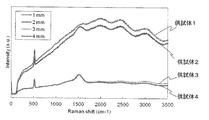
供試体1~4について、薄膜をラマン分光法によって分析した。供試体1~4のラマンスペクトルを図10に示す。ラマン分析は、JIS K 0137:2010「ラマン分光分析通則」を参照してラマン分光測定装置(inVia StreamLine Plus、RENISHAW社製)を用いて分析を行った。
供試体1~4について、薄膜をラマン分光法によって分析した。供試体1~4のラマンスペクトルを図10に示す。ラマン分析は、JIS K 0137:2010「ラマン分光分析通則」を参照してラマン分光測定装置(inVia StreamLine Plus、RENISHAW社製)を用いて分析を行った。
図10に示すように、対向電極間を3mm以上とすることで、ポリマー構造に起因する蛍光が小さくなった。これは、ストリーマ放電は、グロー放電よりもストリーマ内部のイオン密度が多いため、イオン同士の反応がより促進されたことに因ると考えられる。
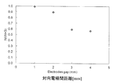
ラマン分析において、N/(N+S)を求め、薄膜中の水素濃度の高低を推測した。対向電極間距離とN/(N+S)との関係を図11に示す。
図11に示すとおり、対向電極間距離を3mm以上とすることで、N/(N+S)が急激に小さくなった。このことから、ストリーマ放電で成膜した薄膜は、グロー放電で成膜した薄膜よりも、薄膜中の水素濃度が低いことが推測できる。これは、ストリーマ放電は、グロー放電よりもストリーマ内部のイオン密度が高いため、イオンの反応がより活性化して水素の引き抜きが起こったことに因ると考えられる。
(実験例4)IR分析
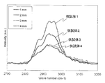
供試体1~4について、薄膜をFTIR(Fourier Transform infrared spectroscopy)法で分析し、対向電極間距離とsp3-CHxピークとの関係を確認した。供試体1~4のFTIRスペクトルを図12に示す。FTIR分析は、赤外分光装置(ALPHA‐T, Bruker Corp.,USA社製)を用いて分析を行った。
供試体1~4について、薄膜をFTIR(Fourier Transform infrared spectroscopy)法で分析し、対向電極間距離とsp3-CHxピークとの関係を確認した。供試体1~4のFTIRスペクトルを図12に示す。FTIR分析は、赤外分光装置(ALPHA‐T, Bruker Corp.,USA社製)を用いて分析を行った。
図12に示すように、対向電極間距離を3mm以上とすることで、C-Hに起因する2800~3000cm-1付近のピーク強度が大幅に減少した。特に、sp3-CH3のピークが弱くなっていることから、Hの減少に伴ってCH3による末端が減少していると考えられる。
(実験例5)表面粗さ
供試体1~4について、薄膜の表面粗さを、走査型プローブ顕微鏡(「SPM-9700」、島津製作所社製)を用い、JIS R 1683:2007「原子間力顕微鏡によるファインセラミックス薄膜の表面粗さ測定方法」に準拠して測定した。表面粗さは、供試体1が0.41nm、供試体2が0.29nm、供試体3が0.19nm、供試体4が0.25nmであった。
供試体1~4について、薄膜の表面粗さを、走査型プローブ顕微鏡(「SPM-9700」、島津製作所社製)を用い、JIS R 1683:2007「原子間力顕微鏡によるファインセラミックス薄膜の表面粗さ測定方法」に準拠して測定した。表面粗さは、供試体1が0.41nm、供試体2が0.29nm、供試体3が0.19nm、供試体4が0.25nmであった。
(実験例6)硬さ
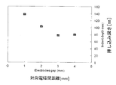
供試体1~4について、薄膜の硬さを評価した。対向電極間距離と押し込み深さとの関係を図13に示す。また、対向電極間距離と押し込み硬度との関係を図19に示す。硬度は、ナノインデンター・システム(「Nano Indenter G200」 Agilent Technologies社製)を用いてISO 14577-2002に準拠してバーコビッチ圧子を使用してナノインデンテーション試験を行い、押し込み深さを測定し、押し込み硬度を算出した。
供試体1~4について、薄膜の硬さを評価した。対向電極間距離と押し込み深さとの関係を図13に示す。また、対向電極間距離と押し込み硬度との関係を図19に示す。硬度は、ナノインデンター・システム(「Nano Indenter G200」 Agilent Technologies社製)を用いてISO 14577-2002に準拠してバーコビッチ圧子を使用してナノインデンテーション試験を行い、押し込み深さを測定し、押し込み硬度を算出した。
図13に示すように、対向電極間距離を増加させるにしたがって、押し込み深さ(Indent depth)が小さくなる傾向が見られた。また、図19に示すように、押し込み深さの値を用いて算出した押し込み硬度(Hardness)は、対向電極間距離が増加するにしたがって高くなる傾向が見られた。特に、対向電極間距離が3mm以上では押し込み硬度が略一定となった。これは、ストリーマ放電は、グロー放電よりもストリーマ内部のイオン密度が高いため、イオンの反応がより活性化して水素の引き抜きが起こり、薄膜中の水素濃度が低くなったことに因ると考えられる。
(供試体5の作製)
図4に示す成膜装置1を用い、対向電極2,12間の距離dを1mmとし、基材4としてSUS304(表面抵抗7×10⁻³オーム/sq、厚さ0.1mm)を電極12の対向面上に配置し、100kPaの圧力下で、反応ガスとしてメタン(CH4)200mL/minと、放電ガスとしてヘリウム(He)4L/minおよびアルゴン(Ar)1L/minとを含む混合ガスを、ガス供給路から供給するとともに、周波数20kHz、パルス幅5μsおよび電圧7kVの電源条件でパルス状電圧を印加して、放電を発生させて基材4の表面に膜厚280nmの薄膜を形成した。成膜時間は120sであった。供試体5の放電形態はグロー放電であった。
図4に示す成膜装置1を用い、対向電極2,12間の距離dを1mmとし、基材4としてSUS304(表面抵抗7×10⁻³オーム/sq、厚さ0.1mm)を電極12の対向面上に配置し、100kPaの圧力下で、反応ガスとしてメタン(CH4)200mL/minと、放電ガスとしてヘリウム(He)4L/minおよびアルゴン(Ar)1L/minとを含む混合ガスを、ガス供給路から供給するとともに、周波数20kHz、パルス幅5μsおよび電圧7kVの電源条件でパルス状電圧を印加して、放電を発生させて基材4の表面に膜厚280nmの薄膜を形成した。成膜時間は120sであった。供試体5の放電形態はグロー放電であった。
(供試体6~8の作製)
対向電極2,12間の距離dを3mm(供試体6),4mm(供試体7),5mm(供試体8)に変更した以外は、供試体5と同様にして基材上に薄膜を形成した。供試体6~8の放電形態はストリーマ放電であった。
対向電極2,12間の距離dを3mm(供試体6),4mm(供試体7),5mm(供試体8)に変更した以外は、供試体5と同様にして基材上に薄膜を形成した。供試体6~8の放電形態はストリーマ放電であった。
供試体5は比較例であり、供試体6~8は本発明品である。
(実験例7)
供試体5~8について実験例3と同様にラマン分析を行った。図15は、供試体5~8のラマンスペクトルである。図16は、対向電極間距離とN/(N+S)との関係を示す。図15に示すとおり、電極間距離が1mmでは、G-bandが確認できなかったが、電極間距離を3mm以上とすることG-bandが確認できた。図16に示すとおり、電極間距離を3mm以上とすることで、N/(N+S)が急激に小さくなった。このように、ストリーマ放電を発生させることで、金属製の基材を用いても良好に成膜できることが確認できた。
供試体5~8について実験例3と同様にラマン分析を行った。図15は、供試体5~8のラマンスペクトルである。図16は、対向電極間距離とN/(N+S)との関係を示す。図15に示すとおり、電極間距離が1mmでは、G-bandが確認できなかったが、電極間距離を3mm以上とすることG-bandが確認できた。図16に示すとおり、電極間距離を3mm以上とすることで、N/(N+S)が急激に小さくなった。このように、ストリーマ放電を発生させることで、金属製の基材を用いても良好に成膜できることが確認できた。
(供試体9の作製)
図4に示す成膜装置1を用い、対向電極2,12間の距離dを5mmとし、基材4として厚さ1.8mmのSiO2上に厚さ1μmのSnO2をコーティングした基材(表面抵抗103オーム/sq)を電極12の対向面上にSnO2コーティング面を上に向けて配置し、100kPaの圧力下で、反応ガスとしてメタン(CH4)200mL/minと、放電ガスとしてヘリウム(He)4L/minおよびアルゴン(Ar)1L/minとを含む混合ガスを、ガス供給路から供給するとともに、周波数30kHz、パルス幅5μsおよび電圧11kVの電源条件でパルス状電圧を印加して、放電を発生させて基材4の表面に膜厚60nmの薄膜を形成した。成膜時間は25sであった。
図4に示す成膜装置1を用い、対向電極2,12間の距離dを5mmとし、基材4として厚さ1.8mmのSiO2上に厚さ1μmのSnO2をコーティングした基材(表面抵抗103オーム/sq)を電極12の対向面上にSnO2コーティング面を上に向けて配置し、100kPaの圧力下で、反応ガスとしてメタン(CH4)200mL/minと、放電ガスとしてヘリウム(He)4L/minおよびアルゴン(Ar)1L/minとを含む混合ガスを、ガス供給路から供給するとともに、周波数30kHz、パルス幅5μsおよび電圧11kVの電源条件でパルス状電圧を印加して、放電を発生させて基材4の表面に膜厚60nmの薄膜を形成した。成膜時間は25sであった。
(供試体10)
成膜時間を50sに変更し膜厚を120nmとした以外は、供試体9の作製と同様にして作製した。
成膜時間を50sに変更し膜厚を120nmとした以外は、供試体9の作製と同様にして作製した。
(供試体11)
成膜時間を100sに変更し膜厚を240nmとした以外は、供試体9の作製と同様にして作製した。
成膜時間を100sに変更し膜厚を240nmとした以外は、供試体9の作製と同様にして作製した。
(供試体12)
基材を厚さSiO2基板(表面抵抗1012オーム/sq、厚さ1.8mm)に変更した以外は、供試体9の作製と同様にして電圧を印加したが、ストリーマ放電は発生せず薄膜は形成されなかった。
基材を厚さSiO2基板(表面抵抗1012オーム/sq、厚さ1.8mm)に変更した以外は、供試体9の作製と同様にして電圧を印加したが、ストリーマ放電は発生せず薄膜は形成されなかった。
供試体9~11は本発明品であり、供試体12は比較例である。
(実験例8)
供試体9~12について実験例3と同様にラマン分析を行った。図17は、供試体9~12のラマンスペクトルである。図18は、成膜時間とN/(N+S)との関係を示す。図17に示すとおり、供試体12は絶縁性のSiO2基板を用いたため成膜できなかったが、供試体9~11は絶縁性のSiO2基板上に導電性のSnO2をコーティングすることでG-bandを有する薄膜を形成することができた。このことから、表面抵抗を所定の範囲に調整することで、基材の材質に関わらず成膜できることが確認できた。図18に示すとおり、供試体9~11は、N/(N+S)が0.7~0.8程度であった。図11に示すSi基板を用いた供試体1~4のN/(N+S)と比較すると(0.5~0.6程度)、供試体9~11の方が少し高かった。
供試体9~12について実験例3と同様にラマン分析を行った。図17は、供試体9~12のラマンスペクトルである。図18は、成膜時間とN/(N+S)との関係を示す。図17に示すとおり、供試体12は絶縁性のSiO2基板を用いたため成膜できなかったが、供試体9~11は絶縁性のSiO2基板上に導電性のSnO2をコーティングすることでG-bandを有する薄膜を形成することができた。このことから、表面抵抗を所定の範囲に調整することで、基材の材質に関わらず成膜できることが確認できた。図18に示すとおり、供試体9~11は、N/(N+S)が0.7~0.8程度であった。図11に示すSi基板を用いた供試体1~4のN/(N+S)と比較すると(0.5~0.6程度)、供試体9~11の方が少し高かった。
(供試体13の作製)
図4に示す成膜装置1を用い、対向電極2,12間の距離dを2mmとし、基材4としてシリコン基材(表面抵抗263オーム/sq、厚さ0.38mm)を電極12の対向面上に配置し、100kPaの圧力下で、反応ガスとしてTrMS(トリメチルシラン)0.5mL/minおよび酸素(O2)0.5L/minと、放電ガスとして窒素(N2)20L/minとを含む混合ガスを、ガス供給路から供給するとともに、周波数30kHz、パルス幅5μsおよび電圧18kVの電源条件でパルス状電圧を印加して、放電を発生させて基材4の表面にSiOx薄膜を形成した。放電形態はストリーマ放電であった。
図4に示す成膜装置1を用い、対向電極2,12間の距離dを2mmとし、基材4としてシリコン基材(表面抵抗263オーム/sq、厚さ0.38mm)を電極12の対向面上に配置し、100kPaの圧力下で、反応ガスとしてTrMS(トリメチルシラン)0.5mL/minおよび酸素(O2)0.5L/minと、放電ガスとして窒素(N2)20L/minとを含む混合ガスを、ガス供給路から供給するとともに、周波数30kHz、パルス幅5μsおよび電圧18kVの電源条件でパルス状電圧を印加して、放電を発生させて基材4の表面にSiOx薄膜を形成した。放電形態はストリーマ放電であった。
供試体13は本発明品である。本発明に係る薄膜形成方法は、反応ガスの種類に関わらず、良好に成膜できることが確認できた。
(供試体14の作製)
図4に示す成膜装置1を用い、対向電極2,12間の距離dを3mmとし、基材4としてシリコン基材(表面抵抗263オーム/sq、厚さ0.38mm)を電極12の対向面上に配置し、100kPaの圧力下で、反応ガスとしてメタン(CH4)400mL/minと、放電ガスとしてヘリウム(He)5L/minを、ガス供給路から供給するとともに、周波数30kHz、パルス幅5μsおよび電圧7kVの電源条件でパルス状電圧を印加して、放電を発生させて基材4の表面に膜厚240nmの薄膜を形成した。成膜時間は100sであった。
図4に示す成膜装置1を用い、対向電極2,12間の距離dを3mmとし、基材4としてシリコン基材(表面抵抗263オーム/sq、厚さ0.38mm)を電極12の対向面上に配置し、100kPaの圧力下で、反応ガスとしてメタン(CH4)400mL/minと、放電ガスとしてヘリウム(He)5L/minを、ガス供給路から供給するとともに、周波数30kHz、パルス幅5μsおよび電圧7kVの電源条件でパルス状電圧を印加して、放電を発生させて基材4の表面に膜厚240nmの薄膜を形成した。成膜時間は100sであった。
(供試体15の作製)
放電ガスをヘリウム(He)4L/minおよびアルゴン(Ar)1L/minとを含む混合ガスに変更した以外は、供試体14の作製と同様にして作製した。
放電ガスをヘリウム(He)4L/minおよびアルゴン(Ar)1L/minとを含む混合ガスに変更した以外は、供試体14の作製と同様にして作製した。
(供試体16の作製)
放電ガスをヘリウム(He)3L/minおよびアルゴン(Ar)2L/minとを含む混合ガスに変更した以外は、供試体14の作製と同様にして作製した。
放電ガスをヘリウム(He)3L/minおよびアルゴン(Ar)2L/minとを含む混合ガスに変更した以外は、供試体14の作製と同様にして作製した。
(供試体17の作製)
放電ガスをヘリウム(He)2L/minおよびアルゴン(Ar)3L/minとを含む混合ガスに変更した以外は、供試体14の作製と同様にして作製した。
放電ガスをヘリウム(He)2L/minおよびアルゴン(Ar)3L/minとを含む混合ガスに変更した以外は、供試体14の作製と同様にして作製した。
(供試体18の作製)
放電ガスをヘリウム(He)1L/minおよびアルゴン(Ar)4L/minとを含む混合ガスに変更した以外は、供試体14の作製と同様にして作製した。
放電ガスをヘリウム(He)1L/minおよびアルゴン(Ar)4L/minとを含む混合ガスに変更した以外は、供試体14の作製と同様にして作製した。
(供試体19の作製)
放電ガスをアルゴン(Ar)5L/minに変更した以外は、供試体14の作製と同様にして作製した。
放電ガスをアルゴン(Ar)5L/minに変更した以外は、供試体14の作製と同様にして作製した。
(実験例10)
供試体14~19について形成された薄膜の押し込み硬度を測定するとともに表面状態を観察した。その結果を表1に示す。表1の結果から、放電ガスの組成は、標準状態の体積比率としてヘリウムを40~100%の範囲で含み、アルゴンを60~0%の範囲で含むことが好ましく、ヘリウムを60~100%の範囲で含み、アルゴンを40~0%の範囲で含むことがより好ましいことが確認された。
供試体14~19について形成された薄膜の押し込み硬度を測定するとともに表面状態を観察した。その結果を表1に示す。表1の結果から、放電ガスの組成は、標準状態の体積比率としてヘリウムを40~100%の範囲で含み、アルゴンを60~0%の範囲で含むことが好ましく、ヘリウムを60~100%の範囲で含み、アルゴンを40~0%の範囲で含むことがより好ましいことが確認された。

上記の実施形態の一部又は全部は、以下の付記のようにも記載されうるが、以下には限られない。
(付記1)
基材の表面に設けられた薄膜において、
該薄膜は、薄膜の内表面から薄膜の外表面に向かうにつれて粒界密度が連続的または断続的に小さくなる傾斜構造を有し、
前記薄膜の前記基材の表面に接する最内部領域は、粒界の粒径が10~30nmである粒界構造を有することを特徴とする薄膜。
基材の表面に設けられた薄膜において、
該薄膜は、薄膜の内表面から薄膜の外表面に向かうにつれて粒界密度が連続的または断続的に小さくなる傾斜構造を有し、
前記薄膜の前記基材の表面に接する最内部領域は、粒界の粒径が10~30nmである粒界構造を有することを特徴とする薄膜。
(付記2)
電圧を印加する電源に接続された第1電極および接地された第2電極からなる一対の対向電極と、該一対の対向電極間に反応ガスおよび放電ガスを含む混合ガスを供給するガス供給路と、を備え、
前記第1電極の対向面は固体誘電体によって覆われている成膜装置を用いた薄膜形成方法において、
前記第2電極の対向面上に、表面抵抗が10-8~103オーム/sqの範囲の基材を設置する工程と、
大気圧または大気圧近傍の圧力下で、前記一対の対向電極間に前記ガス供給路から前記混合ガスを供給するとともに前記電源によって電圧を印加してストリーマ放電を発生させてプラズマCVDで前記基材の表面に薄膜を形成する工程と、を有することを特徴とする薄膜形成方法。
電圧を印加する電源に接続された第1電極および接地された第2電極からなる一対の対向電極と、該一対の対向電極間に反応ガスおよび放電ガスを含む混合ガスを供給するガス供給路と、を備え、
前記第1電極の対向面は固体誘電体によって覆われている成膜装置を用いた薄膜形成方法において、
前記第2電極の対向面上に、表面抵抗が10-8~103オーム/sqの範囲の基材を設置する工程と、
大気圧または大気圧近傍の圧力下で、前記一対の対向電極間に前記ガス供給路から前記混合ガスを供給するとともに前記電源によって電圧を印加してストリーマ放電を発生させてプラズマCVDで前記基材の表面に薄膜を形成する工程と、を有することを特徴とする薄膜形成方法。
(付記3)
前記第2電極の対向面は固体誘電体によって覆われていることを特徴とする付記2に記載の薄膜形成方法。
前記第2電極の対向面は固体誘電体によって覆われていることを特徴とする付記2に記載の薄膜形成方法。
(付記4)
前記電源が印加する電圧は、高周波もしくは休止期間を有するパルス状の電圧であることを特徴とする付記2又は3に記載の薄膜形成方法。
前記電源が印加する電圧は、高周波もしくは休止期間を有するパルス状の電圧であることを特徴とする付記2又は3に記載の薄膜形成方法。
(付記5)
前記高周波またはパルス状の電圧は、交流の波形を有しており、かつその正ピークと負ピークの間の電圧は、前記対向電極間の距離と放電ガス種と圧力によって決定される放電開始電圧の2~10倍で範囲であることを特徴とする付記4に記載の薄膜形成方法。
前記高周波またはパルス状の電圧は、交流の波形を有しており、かつその正ピークと負ピークの間の電圧は、前記対向電極間の距離と放電ガス種と圧力によって決定される放電開始電圧の2~10倍で範囲であることを特徴とする付記4に記載の薄膜形成方法。
(付記6)
前記交流の高周波またはパルス状電圧の周波数は1~100kHzの範囲であり、かつ換算電界が30~1000Tdの範囲であることを特徴とする付記4または5に記載の薄膜形成方法。
前記交流の高周波またはパルス状電圧の周波数は1~100kHzの範囲であり、かつ換算電界が30~1000Tdの範囲であることを特徴とする付記4または5に記載の薄膜形成方法。
(付記7)
前記対向電極間のもっとも近接している対向面の間の距離は3~20mmであることを特徴とする付記2~6のいずれか一つに記載の薄膜形成方法。
前記対向電極間のもっとも近接している対向面の間の距離は3~20mmであることを特徴とする付記2~6のいずれか一つに記載の薄膜形成方法。
(付記8)
前記対向電極は、平板形状に対向させて配置するか、または少なくとも一方の電極が円柱、角柱、円筒または球面状の形状であることを特徴とする付記2~7のいずれか一つに記載の薄膜形成方法。
前記対向電極は、平板形状に対向させて配置するか、または少なくとも一方の電極が円柱、角柱、円筒または球面状の形状であることを特徴とする付記2~7のいずれか一つに記載の薄膜形成方法。
(付記9)
前記反応ガスは、炭素系薄膜を形成する場合は、炭素、水素および/または酸素を含有する化合物、金属酸化物薄膜を形成する場合は、有機金属化合物および酸素であることを特徴とする付記2~8のいずれか一つに記載の薄膜形成方法。
前記反応ガスは、炭素系薄膜を形成する場合は、炭素、水素および/または酸素を含有する化合物、金属酸化物薄膜を形成する場合は、有機金属化合物および酸素であることを特徴とする付記2~8のいずれか一つに記載の薄膜形成方法。
(付記10)
前記炭素系薄膜を形成する場合、メタン、エタンおよびプロパンのいずれか一種もしくはこれらの混合物を反応ガスとすることを特徴とする付記9に記載の薄膜形成方法。
前記炭素系薄膜を形成する場合、メタン、エタンおよびプロパンのいずれか一種もしくはこれらの混合物を反応ガスとすることを特徴とする付記9に記載の薄膜形成方法。
(付記11)
放電ガスは、ヘリウム、アルゴン、窒素の少なくとも1種もしくはこれらの混合物を使用することを特徴とする付記2~10のいずれか一つに記載の薄膜形成方法。
放電ガスは、ヘリウム、アルゴン、窒素の少なくとも1種もしくはこれらの混合物を使用することを特徴とする付記2~10のいずれか一つに記載の薄膜形成方法。
(付記12)
前記放電ガスは、ヘリウムからなるか、又はヘリウムとアルゴンとからなり、前記放電ガスの組成は、標準状態の体積比率としてヘリウムを40~100%の範囲で含み、アルゴンを60~0%の範囲で含むことを特徴とする付記11に記載の薄膜形成方法。
前記放電ガスは、ヘリウムからなるか、又はヘリウムとアルゴンとからなり、前記放電ガスの組成は、標準状態の体積比率としてヘリウムを40~100%の範囲で含み、アルゴンを60~0%の範囲で含むことを特徴とする付記11に記載の薄膜形成方法。
(付記13)
基材が、表面抵抗が103オーム/sqを超える高分子材料からなるとき、前記基材の表面抵抗は、該基材の表面に導電性化合物を付与するか、または前記基材中に導電性化合物を混合して調整することを特徴とする付記2~12に記載の薄膜形成方法。
基材が、表面抵抗が103オーム/sqを超える高分子材料からなるとき、前記基材の表面抵抗は、該基材の表面に導電性化合物を付与するか、または前記基材中に導電性化合物を混合して調整することを特徴とする付記2~12に記載の薄膜形成方法。
1 成膜装置
2 電極(第1電極)
3 固体誘電体
4 基材
5 ガス供給路
6 混合ガス
7 プラズマ化混合ガス
8 排気路
10 薄膜
11A ストリーマ放電
11B グロー放電
12 電極(第2電極)
2 電極(第1電極)
3 固体誘電体
4 基材
5 ガス供給路
6 混合ガス
7 プラズマ化混合ガス
8 排気路
10 薄膜
11A ストリーマ放電
11B グロー放電
12 電極(第2電極)
Claims (4)
- 基材の表面に設けられた薄膜において、
該薄膜は、該薄膜の内表面から該薄膜の外表面に向かうにつれて粒界密度が連続的または断続的に小さくなる傾斜構造を有し、
前記薄膜の前記基材の表面に接する最内部領域は、粒界の粒径が10~30nmである粒界構造を有することを特徴とする薄膜。 - 電圧を印加する電源に接続された第1電極および接地された第2電極からなる一対の対向電極と、該一対の対向電極間に反応ガスおよび放電ガスを含む混合ガスを供給するガス供給路と、を備え、
前記第1電極の対向面は固体誘電体によって覆われている成膜装置を用いた薄膜形成方法において、
前記第2電極の対向面上に、表面抵抗が10-8~103オーム/sqの範囲の基材を設置する工程と、
大気圧または大気圧近傍の圧力下で、前記一対の対向電極間に前記ガス供給路から前記混合ガスを供給するとともに前記電源によって電圧を印加してストリーマ放電を発生させてプラズマCVDで前記基材の表面に薄膜を形成する工程と、を有することを特徴とする薄膜形成方法。 - 前記放電ガスは、ヘリウム、アルゴン、窒素の少なくとも1種もしくはこれらの混合物であることを特徴とする請求項2に記載の薄膜形成方法。
- 前記放電ガスは、ヘリウムからなるか、又はヘリウムとアルゴンとからなり、
前記放電ガスの組成は、標準状態の体積比率としてヘリウムを40~100%の範囲で含み、アルゴンを60~0%の範囲で含むことを特徴とする請求項2に記載の薄膜形成方法。
Priority Applications (1)
| Application Number | Priority Date | Filing Date | Title |
|---|---|---|---|
| JP2017516605A JP6770780B2 (ja) | 2015-05-01 | 2016-04-28 | 薄膜および薄膜形成方法 |
Applications Claiming Priority (2)
| Application Number | Priority Date | Filing Date | Title |
|---|---|---|---|
| JP2015093932 | 2015-05-01 | ||
| JP2015-093932 | 2015-05-01 |
Publications (1)
| Publication Number | Publication Date |
|---|---|
| WO2016178406A1 true WO2016178406A1 (ja) | 2016-11-10 |
Family
ID=57217612
Family Applications (1)
| Application Number | Title | Priority Date | Filing Date |
|---|---|---|---|
| PCT/JP2016/063312 Ceased WO2016178406A1 (ja) | 2015-05-01 | 2016-04-28 | 薄膜および薄膜形成方法 |
Country Status (2)
| Country | Link |
|---|---|
| JP (1) | JP6770780B2 (ja) |
| WO (1) | WO2016178406A1 (ja) |
Citations (3)
| Publication number | Priority date | Publication date | Assignee | Title |
|---|---|---|---|---|
| JP2005123159A (ja) * | 2003-05-27 | 2005-05-12 | Matsushita Electric Works Ltd | プラズマ処理装置、プラズマ生成用の反応器の製造方法、及びプラズマ処理方法 |
| JP2007194110A (ja) * | 2006-01-20 | 2007-08-02 | Ngk Insulators Ltd | 放電プラズマ発生方法 |
| JP2009279778A (ja) * | 2008-05-20 | 2009-12-03 | Konica Minolta Holdings Inc | ハードコート層付積層体 |
Family Cites Families (1)
| Publication number | Priority date | Publication date | Assignee | Title |
|---|---|---|---|---|
| JP3555470B2 (ja) * | 1998-12-04 | 2004-08-18 | セイコーエプソン株式会社 | 大気圧高周波プラズマによるエッチング方法 |
-
2016
- 2016-04-28 JP JP2017516605A patent/JP6770780B2/ja not_active Expired - Fee Related
- 2016-04-28 WO PCT/JP2016/063312 patent/WO2016178406A1/ja not_active Ceased
Patent Citations (3)
| Publication number | Priority date | Publication date | Assignee | Title |
|---|---|---|---|---|
| JP2005123159A (ja) * | 2003-05-27 | 2005-05-12 | Matsushita Electric Works Ltd | プラズマ処理装置、プラズマ生成用の反応器の製造方法、及びプラズマ処理方法 |
| JP2007194110A (ja) * | 2006-01-20 | 2007-08-02 | Ngk Insulators Ltd | 放電プラズマ発生方法 |
| JP2009279778A (ja) * | 2008-05-20 | 2009-12-03 | Konica Minolta Holdings Inc | ハードコート層付積層体 |
Also Published As
| Publication number | Publication date |
|---|---|
| JPWO2016178406A1 (ja) | 2018-03-01 |
| JP6770780B2 (ja) | 2020-10-21 |
Similar Documents
| Publication | Publication Date | Title |
|---|---|---|
| Hegemann et al. | Deposition of SiOx films from O2/HMDSO plasmas | |
| CN104023971B (zh) | 阻气膜和阻气膜的制造方法 | |
| CN103958183B (zh) | 阻气膜和阻气膜的制造方法 | |
| Hubert et al. | Synthesis and texturization processes of (super)-hydrophobic fluorinated surfaces by atmospheric plasma | |
| CN1525912A (zh) | 铟锡氧化物的透明导电层状镀层 | |
| US20140099451A1 (en) | Method for depositing layers on a glass substrate by means of low-pressure pecvd | |
| EP2383366A1 (en) | Method for producing diamond-like carbon membrane | |
| Imai et al. | Hydrogen-free fluorinated DLC films with high hardness prepared by using T-shape filtered arc deposition system | |
| JPWO2008044474A1 (ja) | 透明導電膜の形成方法 | |
| CN100559513C (zh) | 透明导电膜 | |
| Abou Rich et al. | LDPE surface modifications induced by atmospheric plasma torches with linear and showerhead configurations | |
| Silva et al. | DLC films grown on steel using an innovator active screen system for PECVD technique | |
| Koerner et al. | Influence of RF plasma reactor setup on carboxylated hydrocarbon coatings | |
| JP5295102B2 (ja) | 導電性保護膜及びその製造方法 | |
| Lee et al. | Enhancement of barrier properties of aluminum oxide layer by optimization of plasma-enhanced atomic layer deposition process | |
| Vandentop et al. | Observation of the initial stages of growth of hydrogenated amorphous carbon films by scanning tunneling microscopy | |
| Shearer et al. | Composite SiO2/TiO2 and amine polymer/TiO2 nanoparticles produced using plasma-enhanced chemical vapor deposition | |
| Lin et al. | Characterization of the silicon oxide thin films deposited on polyethylene terephthalate substrates by radio frequency reactive magnetron sputtering | |
| Kuzminova et al. | Barrier coatings on polymeric foils for food packaging | |
| JPWO2008044473A1 (ja) | 透明導電膜の成膜方法及び透明導電膜基板 | |
| Lee et al. | UV-enhanced atomic layer deposition of ZrO2 thin films at room temperature | |
| Zimmermann et al. | High rate deposition of amorphous hydrogenated carbon films by hollow cathode arc PECVD | |
| JP6770780B2 (ja) | 薄膜および薄膜形成方法 | |
| Bae et al. | High-speed deposition of graphite-like carbon film by Ar/C6H6 surface-wave plasma with high-voltage pulse biasing | |
| Liu et al. | Properties and deposition processes of aC: H films from CH4/Ar dielectric barrier discharge plasmas |
Legal Events
| Date | Code | Title | Description |
|---|---|---|---|
| 121 | Ep: the epo has been informed by wipo that ep was designated in this application |
Ref document number: 16789542 Country of ref document: EP Kind code of ref document: A1 |
|
| ENP | Entry into the national phase |
Ref document number: 2017516605 Country of ref document: JP Kind code of ref document: A |
|
| NENP | Non-entry into the national phase |
Ref country code: DE |
|
| 122 | Ep: pct application non-entry in european phase |
Ref document number: 16789542 Country of ref document: EP Kind code of ref document: A1 |