WO2016171407A1 - 슈퍼커패시터 및 이의 제조 방법 - Google Patents
슈퍼커패시터 및 이의 제조 방법 Download PDFInfo
- Publication number
- WO2016171407A1 WO2016171407A1 PCT/KR2016/003197 KR2016003197W WO2016171407A1 WO 2016171407 A1 WO2016171407 A1 WO 2016171407A1 KR 2016003197 W KR2016003197 W KR 2016003197W WO 2016171407 A1 WO2016171407 A1 WO 2016171407A1
- Authority
- WO
- WIPO (PCT)
- Prior art keywords
- thin film
- carbon
- supercapacitor
- current collectors
- carbon nano
- Prior art date
- Legal status (The legal status is an assumption and is not a legal conclusion. Google has not performed a legal analysis and makes no representation as to the accuracy of the status listed.)
- Ceased
Links
Images




Classifications
-
- H—ELECTRICITY
- H01—ELECTRIC ELEMENTS
- H01G—CAPACITORS; CAPACITORS, RECTIFIERS, DETECTORS, SWITCHING DEVICES, LIGHT-SENSITIVE OR TEMPERATURE-SENSITIVE DEVICES OF THE ELECTROLYTIC TYPE
- H01G11/00—Hybrid capacitors, i.e. capacitors having different positive and negative electrodes; Electric double-layer [EDL] capacitors; Processes for the manufacture thereof or of parts thereof
- H01G11/54—Electrolytes
- H01G11/58—Liquid electrolytes
-
- H—ELECTRICITY
- H01—ELECTRIC ELEMENTS
- H01G—CAPACITORS; CAPACITORS, RECTIFIERS, DETECTORS, SWITCHING DEVICES, LIGHT-SENSITIVE OR TEMPERATURE-SENSITIVE DEVICES OF THE ELECTROLYTIC TYPE
- H01G11/00—Hybrid capacitors, i.e. capacitors having different positive and negative electrodes; Electric double-layer [EDL] capacitors; Processes for the manufacture thereof or of parts thereof
- H01G11/66—Current collectors
- H01G11/68—Current collectors characterised by their material
-
- H—ELECTRICITY
- H01—ELECTRIC ELEMENTS
- H01G—CAPACITORS; CAPACITORS, RECTIFIERS, DETECTORS, SWITCHING DEVICES, LIGHT-SENSITIVE OR TEMPERATURE-SENSITIVE DEVICES OF THE ELECTROLYTIC TYPE
- H01G11/00—Hybrid capacitors, i.e. capacitors having different positive and negative electrodes; Electric double-layer [EDL] capacitors; Processes for the manufacture thereof or of parts thereof
- H01G11/84—Processes for the manufacture of hybrid or EDL capacitors, or components thereof
-
- Y—GENERAL TAGGING OF NEW TECHNOLOGICAL DEVELOPMENTS; GENERAL TAGGING OF CROSS-SECTIONAL TECHNOLOGIES SPANNING OVER SEVERAL SECTIONS OF THE IPC; TECHNICAL SUBJECTS COVERED BY FORMER USPC CROSS-REFERENCE ART COLLECTIONS [XRACs] AND DIGESTS
- Y02—TECHNOLOGIES OR APPLICATIONS FOR MITIGATION OR ADAPTATION AGAINST CLIMATE CHANGE
- Y02E—REDUCTION OF GREENHOUSE GAS [GHG] EMISSIONS, RELATED TO ENERGY GENERATION, TRANSMISSION OR DISTRIBUTION
- Y02E60/00—Enabling technologies; Technologies with a potential or indirect contribution to GHG emissions mitigation
- Y02E60/13—Energy storage using capacitors
Definitions
- the present invention relates to a supercapacitor and a method of manufacturing the same, and more particularly, to a supercapacitor that can be used as an AC line filtering element and a method of manufacturing the supercapacitor.
- the components constituting the AC line filtering element is an aluminum electrolytic capacitor.
- the aluminum electrolytic capacitor occupies the largest volume of the components.
- the aluminum electrolytic capacitor applied to the AC line filtering device requires a high energy density per unit volume. Therefore, miniaturization of an aluminum electrolytic capacitor, which occupies a relatively large volume among components constituting the AC line filtering element, is required.
- supercapacitors or electric double layer capacitors (EDLC) have a higher energy density per volume than aluminum electrolytic capacitors.
- the supercapacitor is considered as a substitute to replace the aluminum electrolytic capacitor.
- One object of the present invention is to provide a supercapacitor having an improved response speed and energy density per unit volume and an increased operating voltage range.
- One object of the present invention is to provide a method of manufacturing the supercapacitor.
- the current collectors provided to face each other spaced apart, the organic electrolyte layer interposed between the current collector, the organic electrolyte layer partitions the electrical between the current collector And a carbon nano thin film made of a carbon nano material aligned in a direction substantially parallel to the upper surface on a separator for suppressing a short circuit and on an upper surface of each of the current collectors.
- the carbon nanomaterial may include carbon nanotubes or graphene.
- the carbon nano thin film may have a pore structure having a thickness in the range of 50 to 300 nm and a pore size distribution in the range of 2 to 50 nm.
- the current collector may have a laminated structure in which a titanium thin film and a gold thin film are sequentially stacked between aluminum foils.
- the organic electrolyte layer may include an alkyl salt and an ACN organic solvent.
- a supercapacitor In the method of manufacturing a supercapacitor according to embodiments of the present invention, after preparing current collectors, carbon nanomaterials are arranged on a top surface of each of the current collectors in a direction substantially parallel to the top surface. Each of the carbon nano thin films is formed. After arranging the current collectors to face each other, an organic electrolyte layer and the organic electrolyte layer are partitioned between the current collectors to form a separator for suppressing a short circuit between the current collectors.
- the dispersion in order to form the carbon nano thin film, after dispersing the carbon nanomaterial in a solution to form a dispersion, the dispersion is formed on the template through a vacuum filtration process on the template.
- the template on which the carbon nanofilm is formed is suspended on a basic solution to remove the template and leave the carbon nanofilm. Thereafter, the basic solution is diluted and converted into a neutral solution, and then each of the current collectors in which a thin gold film is formed on an aluminum foil is immersed in the neutral solution. Thereafter, the neutral solution is removed while each of the current collectors is immersed to form a carbon nano thin film on the gold thin film.
- the dispersion may be formed using an ultrasonic mill without a dispersion.
- the aluminum foil in order to form each of the current collector, may be surface-etched, and a titanium thin film and a gold thin film may be sequentially formed on the surface-etched aluminum foil.
- the gold thin film and the titanium thin film may be formed through an electron beam vacuum deposition process.
- the supercapacitor according to the embodiments of the present invention as described above may include an carbon nano thin film and an organic electrolyte layer, thereby increasing energy density per volume and improving frequency response characteristics.
- the thickness of the carbon nano thin film can be adjusted according to the maximum capacitance or energy density per volume applicable to the AC line filtering. That is, as the supercapacitor has an increased capacitance per volume and an operating voltage range, an energy density per volume may be 100 to 1000 times higher than that of a conventional supercapacitor.
- the driving voltage can be extended to 2.5V.
- the supercapacitor is applied to a low voltage AC line filtering element of 21 V or less, the capacitance per volume is higher than that of a conventional aluminum electrolytic capacitor.
- 1 is a schematic diagram showing the electrode density and frequency response characteristics of the supercapacitor according to the alignment direction and thickness of the carbon nanomaterial in the carbon nanotube (CNT) film formed on the substrate.
- FIG. 2 is a photograph for explaining a process of forming a carbon nanotube thin film on a current collector according to an embodiment of the present invention.
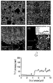
- FIG. 3 is electron micrographs showing a surface where a carbon nanotube thin film (electrode) is formed on a current collector.
- 5 to 8 are graphs for explaining the frequency response characteristics according to the electrode thickness of the carbon nanotube supercapacitor (Example).
- Example 9 is a graph showing a board diagram of a carbon nanotube supercapacitor (Example) and an aluminum electrolytic capacitor (Comparative Example 1).
- a carbon nanotube supercapacitor including a current collector in which a titanium thin film and a gold thin film are sequentially stacked on an aluminum foil, and a supercapacitor (comparative example 2) formed by using an aluminum foil as a current collector.
- This is a board diagram showing the phase angle.
- 15 is a graph showing the pore size distribution of carbon nanotube powder.
- FIG. 16 is a graph illustrating a change in capacitance per volume according to cell voltages of a carbon nanotube supercapacitor (example) and an aluminum electrolytic capacitor.
- the current collectors provided to face each other spaced apart, the organic electrolyte layer interposed between the current collector, the organic electrolyte layer partitions the electrical between the current collector And a carbon nano thin film made of a carbon nano material aligned in a direction substantially parallel to the upper surface on a separator for suppressing a short circuit and on an upper surface of each of the current collectors.
- first and second may be used to describe various components, but the components should not be limited by the terms. The terms are used only for the purpose of distinguishing one component from another.
- the first component may be referred to as the second component, and similarly, the second component may also be referred to as the first component.
- a supercapacitor according to embodiments of the present invention includes current collectors, carbon nano thin films, separators, and organic electrolyte layers.
- the supercapacitor may have a form of a cylinder type or a plate type.
- the current collectors are provided to face each other apart from each other.
- the current collectors may apply a voltage to ions dissociated in the organic electrolyte layer.
- Each of the current collectors may have a laminated structure in which a titanium thin film and an Au thin film are sequentially stacked on an aluminum foil.
- the gold element included in the gold thin film is a material that forms an excellent electrical contact with the carbon nano thin film.
- electrical contact between the carbon nano thin film and the aluminum foil may be improved. That is, depending on the type of metal in contact with the carbon nano thin film such as carbon nanotubes or graphene, the metal wettablity and Schottky barrier height, and also the interface and device characteristics may be affected. Considering that the gold thin film may be additionally formed.
- a titanium thin film may be used as an adhesion layer between the gold thin film and the aluminum foil.
- the organic electrolyte layer is interposed between the current collectors.
- the organic electrolyte layer is made of an organic electrolyte material.
- the organic electrolyte material replaces the existing aqueous electrolyte material so that the supercapacitor can have an extended operating voltage range.
- the supercapacitor made of the aqueous electrolyte material has an operating range of about 1.23 V, whereas in the case of the supercapacitor including the organic electrolyte layer and the carbon nano thin film, ions dissociated from the organic electrolyte layer have a pore structure.
- the supercapacitor including the organic electrolyte layer and the carbon nano thin film may have an operating voltage range of up to 2.5V.
- the organic electrolyte layer may be formed of an alkyl salt and an ACN organic solvent.
- the alkyl salt may include tetraethylammonium, tetrabutylammonium or tetramethylammonium as a cation.
- examples of the alkyl salt include tetraethylammonium tetrafluoroborate (TEABF 4 ).
- the separator is provided in the organic electrolyte layer.
- the separator partitions the organic electrolyte layer.
- the separator may suppress electrical short between the current collectors.
- the carbon nano thin film is formed on an upper surface of each of the current collectors.
- the carbon nano thin film is made of carbon nano material aligned in a direction substantially parallel to the upper surface of the current collectors.
- the carbon nano thin film functions as an electrode of a supercapacitor.
- the carbon nanomaterial When the carbon nanomaterial is aligned in a direction perpendicular to the upper surface (see FIG. 1A), the carbon nanomaterial may have a macroporous pore structure. In this case, the response speed is high, but since the pore size of 50 nm or more is formed, the energy density per volume may be low.
- the carbon nano thin film is aligned in a direction substantially parallel to the upper surface, the pore size may be reduced. As a result, the energy density per volume may be increased while the response speed may be reduced (see FIG. 1B).
- the carbon nano thin film may have a thickness in the range of 50 to 300 nm.
- the carbon nano thin film may have an improved energy density per volume and response speed.
- the carbon nano thin film may have a pore structure having a pore size distribution in the range of 2 to 50 nm.
- the carbon nanomaterial may include carbon nanotubes or graphene.
- the carbon nanotubes may include single-walled carbon nanotubes, double-walled carbon nanotubes, multiwalled carbon nanotubes, thin multiwalled carbon nanotubes, and bundle carbon nanotubes.
- FIG. 2 is a photograph for explaining a process of forming a carbon nanotube thin film on a current collector according to an embodiment of the present invention.
- the current collector may be formed using a metal material.
- the current collector may be formed by sequentially forming a titanium thin film and a gold thin film on an aluminum foil.
- the surface of the aluminum foil is etched to treat the surface of the aluminum foil. This may increase the surface roughness of the surface of the aluminum foil to increase the bonding strength with the carbon nano thin film formed subsequently.
- a titanium thin film and a gold thin film are sequentially formed on the surface-treated aluminum foil.
- the titanium thin film and the gold thin film may be formed through an electron beam vacuum deposition process.
- a current collector in which a titanium thin film and a gold thin film are sequentially formed is formed on the aluminum foil.
- the gold thin film may be improved in electrical contact properties by contact with a subsequently formed carbon nano thin film.
- each of the carbon nano thin films made of carbon nanomaterials aligned in a direction substantially parallel to the upper surface is formed on the upper surface of each of the current collectors.
- the carbon nanomaterial is dispersed in a solution to form a dispersion.
- a solution for example, carbon nanotubes may be used as the carbon nanomaterial.
- the solution may be made of a propylene carbonate material.
- the dispersion may be formed using an ultrasonic grinder without a separate dispersion. (See FIG. 2A)
- the dispersion is then formed on a template through a vacuum filtration process to form a carbon nanofilm. That is, the dispersion is poured onto the template and the carbon nanomaterials contained in the dispersion are coated on the template surface through a vacuum filtration process. As a result, a carbon nanofilm is uniformly formed on the template.
- the template may be formed using a material and the ennodic aluminum oxide. (See Figure 2 (b))
- the template on which the carbon nanofilm is formed is then suspended on a basic solution such as sodium hydroxide solution to remove the template and leave the carbon nanofilm in the basic solution. (See Figure 2 (c))
- the collectors on which the carbon nano thin films are formed are disposed to face each other.
- the supercapacitor may have a cylindrical shape or a plate shape according to the arrangement.
- an organic electrolyte layer and the organic electrolyte layer are partitioned between the current collectors to form a separator to suppress a short circuit between the current collectors, thereby manufacturing a supercapacitor.
- the organic electrolyte layer may be formed using an organic electrolyte including an alkyl salt and an ACN organic solvent.
- the alkyl salt may include tetraethylammonium, tetrabutylammonium or tetramethylammonium as a cation.
- examples of the alkyl salt include tetraethylammonium tetrafluoroborate (TEABF 4 ).
- the carbon nano thin film is formed on the current collector through the vacuum filtration process as described above, a plasma enhanced chemical vapor deposition (PECVD) process for manufacturing graphene and carbon nanotubes aligned in a conventional vertical direction or Compared to a thermal CVD process, the simplicity can improve the economics. Furthermore, the thickness of the carbon nano thin film may be adjusted by controlling the amount of carbon nano material included in the dispersion.
- PECVD plasma enhanced chemical vapor deposition
- the ions dissociated from the organic electrolyte layer may have an increased operating voltage range by having a suitable accessibility to the carbon nano thin film having a pore structure.
- the supercapacitor including the organic electrolyte layer and the carbon nano thin film may have an operating voltage range up to 2.5V.
- SWCNTs single-walled carbon nanotubes
- AAO enodic aluminum oxide template
- the carbon nanotube film remaining in the neutral solution was formed as an electrode on the aluminum current collector.
- the thickness of the carbon nanotube film functioning as an electrode was adjusted from 53 nm to 298 nm, respectively.
- a supercapacitor was manufactured using a two-electrode carbon nanotube electrode / current collector, an organic electrolyte layer, and a separator formed in the above-described preparation example in a glove box.
- the organic electrolyte was used by dissolving 1M tetraethylammonium tetrafluoroborate (TEABF 4 ) in acetonitrile.
- TEABF 4 1M tetraethylammonium tetrafluoroborate
- PTFE Polytetrafluoroethylene
- the shape and thickness of the carbon nanotube films were analyzed by electron scanning microscope (SEM) and atomic force microscope (AFM).
- SEM electron scanning microscope
- AFM atomic force microscope
- the specific surface area and pore size distribution of carbon nanotube powders are obtained through Brunauer-Emmett-Teller (BET) and Barrett-Joiner-Hilda (BJH).
- Cyclic voltammetry, constant current charge and discharge, and electrochemical impedance spectroscopy are performed.
- the frequency response is driven by a direct current of 0 V and an alternating current of 10 mV. All electrochemical measurements are made with a two-electrode system. Electrochemical measurements of aluminum electrolytic capacitors are made for comparison with carbon nanotube supercapacitors.
- 3 is electron micrographs showing the surface of the carbon nanotube thin film formed on the current collector.
- 3 (a) and 3 (b) are low and high magnification scanning electron micrographs of a carbon nanotube film coated on a current collector including gold / titanium / aluminum foil.
- the dark areas are pores generated during the etching process to expand the surface area of the aluminum foil. These pores range in size from several nm to several tens of ⁇ m. It can be seen that the carbon nanotube film covers the entire surface of the metal current collector by covering the pores of the aluminum foil.
- a cross section of a very thin carbon nanotube is shown on the etched aluminum foil in FIG.
- the thickness of the carbon nanotube film was prepared from 53 to 298 nm, which corresponds to a mass of 4 to 32 ⁇ g of carbon nanotube film. (See Figure 4)
- the density of the carbon nanotube increases from 0.75 g / cc to 1.08 g / cc. This corresponds to 48.7% to 70.1% of theoretical density (1.54 g / cc) when the diameter of single-walled carbon nanotubes is 1 nm.
- 5 to 8 are graphs for explaining the frequency response characteristics according to the electrode thickness of the carbon nanotube supercapacitor (Example).
- 9 is a graph showing a board diagram of a carbon nanotube supercapacitor (Example) and an aluminum electrolytic capacitor (Comparative Example 1).
- the organic electrolyte and the carbon nanotube supercapacitors have a frequency response characteristic fast enough for an AC line filtering application.
- the 120 Hz phase angle of the supercapacitor having a thickness of 53 nm to 298 nm ranges from -82.2 ° to -84.3 °.
- the Nyquist plot shows nearly vertical behavior and low equivalent series resistance (0.22 to 0.26 ⁇ ), which means that all supercapacitors exhibit capacitor behavior.
- the absence of a semicircle and a -45 ° line in the high frequency region means physical adsorption and desorption of ions with very fast charge storage.
- the pore structure of the carbon nanotube film contributes to the rapid movement of electrolyte ions.
- the frequency response characteristic and capacitance per area of the supercapacitor vary with the electrode thickness. As the electrode thickness decreases, the response speed increases, but the capacitance decreases.
- an appropriate thickness capable of maintaining the maximum capacitance while maintaining a high phase angle ( ⁇ -80 °, 120 Hz) is important (see FIG. 7). That is, as the thickness of the carbon nanotube film is increased from 53 to 298 nm, the capacitance increases about 58 times from 58 to 282 ⁇ F / cm 2 .
- the time constant increases from 60 to 500 ⁇ s. This is because the time constant increases because the pore structure, which is the distance required to move the electrolyte ions during charge and discharge, increases as the electrode thickness increases.
- Supercapacitors with relatively short time constants can serve as sufficient AC line filtering at 120 Hz.
- FIG. 10 is a phase angle of a carbon nanotube supercapacitor (example) including a current collector in which a titanium thin film and a gold thin film are sequentially formed on an aluminum foil and a supercapacitor (comparative example 2) using an aluminum foil as a metal current collector.
- a carbon nanotube supercapacitor including a current collector in which a titanium thin film and a gold thin film are sequentially formed on an aluminum foil and a supercapacitor (comparative example 2) using an aluminum foil as a metal current collector.
- an aluminum current collector may additionally deposit a gold thin film in contact with the carbon nanotube thin film, thereby exhibiting a very high frequency response even when an organic electrolyte is used.
- An aluminum current collector (Comparative Example 2) made of aluminum foil without a gold thin film has a phase angle of approximately -34 ° at 120 Hz, which makes it difficult to use AC line filtering.
- the supercapacitor in order for the supercapacitor to have improved frequency response characteristics, it is possible to further deposit a titanium thin film and a gold thin film on the aluminum foil.
- gold (Au) forming the gold thin film forms an improved electrical contact with the carbon nanotubes. Therefore, the electrical contact may be improved as the carbon nanotubes are exposed to the gold thin film.
- the cyclic voltammogram maintains a rectangular shape even at a high scanning speed of 450 V / s (32 ⁇ g / cm 2). As the scan rate is increased from 50 to 450 V / s, the capacitance per volume decreases approximately 20% from 10.9 to 8.8 F / cc.
- the constant current charge / discharge curve of FIG. 13 shows a triangular shape and almost no IR drop in a wide current density range.
- the carbon nanotube supercapacitor has an improved speed capability with excellent frequency response.
- the carbon nanotube supercapacitor according to the embodiments of the present invention shows the highest energy density per volume (4.11 mWh / cc) among the 120 Hz line filtering supercapacitors developed so far. These results show energy densities that are 100-1000 times higher than previously reported.
- graphene and carbon nanotube structures vertically aligned with respect to the current collector surface exhibit high phase angles from -82 ° to -85 ° at 120 Hz, but have an energy density per volume (0.04 to 0.1 mWh / cc) is low.
- supercapacitors made of carbon black or graphene quantum dots also show low energy density of 0.2 to 0.4 mWh / cc and have a low phase angle of -75 ° at 120 Hz.
- 15 is a graph showing the pore size distribution of carbon nanotube powder.
- a carbon nanotube supercapacitor according to embodiments of the present invention has improved frequency response. This may be due to the pore structure of the electrode material relatively large compared to the size of the electrolyte ions.
- BET Brunauer-Emmett-Teller
- BJH Barrett-Joiner-Hellenda
- the size of the solvated ions of TEA + and BF 4 ⁇ are approximately 1.3 nm and 1.16 nm.
- the dissociated ions in the electrolyte have excellent mobility in the macroporous structure of the carbon nanotubes.
- FIG. 16 is a graph illustrating a change in capacitance per volume according to cell voltages of a carbon nanotube supercapacitor (example) and an aluminum electrolytic capacitor.
- the large specific surface area (1125.3 m 2 / g) of the carbon nanotubes contributes to the high capacitance of the supercapacitor.
- Supercapacitors with carbon nanotubes show a capacitance per volume (25.5 mF / cc to 3.0 mF / cc) at 2.5 V, 8.5 times higher than commercial aluminum electrolytic capacitors (AEC). Connecting a 2.5 V supercapacitor in series or increasing the dielectric layer thickness of an aluminum electrolytic capacitor can increase the operating voltage.
- Such supercapacitors can be usefully used in small electronic devices requiring excellent frequency characteristics.
Landscapes
- Engineering & Computer Science (AREA)
- Power Engineering (AREA)
- Chemical & Material Sciences (AREA)
- Microelectronics & Electronic Packaging (AREA)
- Chemical Kinetics & Catalysis (AREA)
- Electrochemistry (AREA)
- Materials Engineering (AREA)
- Manufacturing & Machinery (AREA)
- Electric Double-Layer Capacitors Or The Like (AREA)
Abstract
슈퍼커패시터는, 상호 이격되어 마주보도록 구비된 집전체들, 상기 집전체들 사이에 개재된 유기 전해질층, 상기 유기 전해질층을 구획하여 상기 집전체들 사이의 전기적인 단락을 억제하는 분리막 및 상기 집전체들 각각의 상부 표면 상에 상기 상부 표면에 대하여 실질적으로 평행한 방향으로 정렬된 탄소 나노 물질로 이루어진 탄소 나노 박막을 포함한다. 따라서, 작동 전압이 2.5V까지 확장된 상태에서 개선된 부피당 에너지 밀도 및 주파수 응답속도를 갖는 교류라인 필터링 소자가 구현될 수 있다.
Description
본 발명은 슈퍼커패시터 및 이의 제조 방법에 관한 것으로, 보다 상세하게는 교류 라인 필터링 소자로 이용될 수 있는 슈퍼커패시터 및 상기 슈퍼커패시터의 제조 방법에 관한 것이다.
교류 라인 필터링 소자를 구성하는 부품들 중 알루미늄 전해 커패시터가 있다. 특히, 상기 알루미늄 전해 커패시터는 상기 부품들 중 가장 큰 부피를 차지한다. 또한, 상기 교류 라인 필터링(AC line filtering) 소자에 적용되는 알루미늄 전해 커패시터는, 높은 단위 부피당 에너지밀도를 요구한다. 따라서 상기 교류 라인 필터링 소자를 이루는 부품들 중 상대적으로 큰 부피를 차지하는 알루미늄 전해 커패시터의 소형화가 요구된다.
한편, 슈퍼커패시터, 또는 전기이중층 커패시터(electric double layer capacitor; EDLC)는 알루미늄 전해 커패시터보다 높은 부피당 에너지 밀도를 가진다. 상기 슈퍼커패시터는 상기 알루미늄 전해 커패시터를 대체할 수 있는 대체물로서 고려되고 있다.
하지만 일반적인 전기이중층 커패시터는 매우 느린 주파수 응답 특성 때문에 교류 라인 필터링 소자의 부품으로 적용하는데 어려움이 있다. 즉, 일반적인 전기이중층 커패시터는 활성 탄소를 전극물질로 이용하지만 복잡하고 좁은 기공구조로 인해 전해질 이온의 이동이 제한되어 주파수 응답특성 속도가 저하되는 문제가 있다.
상기 슈퍼커패시터와 관련된 선행문헌으로는 대한민국 공개특허공보 제10-2014-0011485호(공개일자:2014.01.29.)가 있다.
본 발명의 일 목적은 개선된 응답 속도와 단위부피당 에너지 밀도를 갖고 증대된 작동 전압 범위를 갖는 슈퍼커패시터를 제공하는 것이다.
본 발명의 일 목적은 상기 슈퍼커패시터의 제조 방법을 제공하는 것이다.
본 발명의 실시예들에 따른 슈퍼커패시터는, 상호 이격되어 마주보도록 구비된 집전체들, 상기 집전체들 사이에 개재된 유기 전해질층, 상기 유기 전해질층을 구획하여 상기 집전체들 사이의 전기적인 단락을 억제하는 분리막 및 상기 집전체들 각각의 상부 표면 상에 상기 상부 표면에 대하여 실질적으로 평행한 방향으로 정렬된 탄소 나노 물질로 이루어진 탄소 나노 박막을 포함한다.
본 발명의 일 실시예에 있어서, 상기 탄소 나노 물질은 탄소 나노 튜브 또는 그래핀을 포함할 수 있다.
본 발명의 일 실시예에 있어서, 상기 탄소 나노 박막은 50 내지 300 nm 범위의 두께 및 2 내지 50 nm 범위의 기공 크기 분포를 갖는 기공 구조를 가질 수 있다.
본 발명의 일 실시예에 있어서, 상기 집전체는 알루미늄 호일 사이에 티타늄 박막 및 금 박막이 순차적으로 적층된 적층 구조를 가질 수 있다.
본 발명의 일 실시예에 있어서, 상기 유기 전해질층은 알킬계 염 및 ACN 유기 용매를 포함할 수 있다.
본 발명의 실시예들에 따른 슈퍼커패시터의 제조 방법에 있어서, 집전체들을 준비한 후, 상기 집전체들 각각의 상부 표면 상에 상기 상부 표면에 대하여 실질적으로 평행한 방향으로 정렬된 탄소 나노 물질로 이루어진 탄소 나노 박막들 각각을 형성한다. 상기 집전체들을 상호 마주보도록 배치한 후, 상기 집전체들 사이에 유기 전해질층과 상기 유기 전해질층을 구획하여 상기 집전체들 사이의 단락을 억제하는 분리막을 형성한다.
본 발명의 일 실시예에 있어서, 상기 탄소 나노 박막을 형성하기 위하여, 탄소 나노 물질을 용액 내에 분산시켜 분산액을 형성한 후, 상기 분산액을 진공 여과 공정을 통하여 템플릿 상에 탄소 나노 필름을 형성한다. 상기 탄소 나노 필름이 형성된 템플릿을 염기성 용액 상에 부유시켜, 상기 템플릿을 제거하고 상기 탄소 나노 필름을 잔류시킨다. 이후, 상기 염기성 용액을 희석하여 중성 용액으로 변환시킨 후, 상기 중성 용액 내에, 알루미늄 호일 상에 금 박막이 형성된 집전체들 각각을 침지시킨다. 이후, 상기 집전체들 각각이 침지된 상태에서 상기 중성 용액을 제거하여 상기 금 박막 상에 탄소 나노 박막을 형성한다.
여기서, 상기 분산액은, 분산재 없이 초음파 분쇄기를 이용하여 형성될 수 있다.
본 발명의 일 실시예에 있어서, 상기 집전체들 각각을 형성하기 위하여, 알루미늄 호일을 표면 식각하고, 상기 표면 식각된 알루미늄 호일 상에 티타늄 박막 및 금 박막이 순차적으로 각각 형성될 수 있다.
여기서, 상기 금 박막 및 티타늄 박막은 전자빔 진공 증착 공정을 통하여 형성될 수 있다.
상기와 같은 본 발명의 실시예들에 따른 슈퍼커패시터는 탄소 나노 박막 및 유기 전해질층을 포함함으로써 부피당 에너지 밀도가 증가하며 주파수 응답특성이 개선될 수 있다. 또한 탄소 나노 박막의 두께는 교류 라인 필터링에 적용 가능한 최대 부피당 정전용량 또는 에너지 밀도에 따라 조절될 수 있다. 즉, 슈퍼커패시터가 증대된 부피당 정전용량과 작동 전압범위를 가짐에 따라 종래의 슈퍼커패시터보다 100~1000배 높은 부피당 에너지 밀도를 구현할 수 있다.
한편, 상기 탄소 나노 박막의 기공 구조가 유기 전해질에 적합하기 때문에 구동 전압이 2.5 V 까지 확장 될 수 있다. 상기 슈퍼커패시터가 21 V 이하의 저전압 교류라인 필터링 소자에 적용될 경우, 부피당 정전용량이 종래의 알루미늄 전해 커패시터보다 높다.
도 1은 기판 상에 형성된 탄소나노튜브 (CNT) 필름 내의 탄소 나노 물질의 정렬 방향 및 두께에 따라 슈퍼커패시터의 전극밀도와 주파수 응답특성을 나타낸 모식도이다.
도 2는 본 발명의 일 실시예에 따른 집전체 상에 탄소 나노 튜브 박막을 형성하는 공정을 설명하기 위한 사진들이다.
도 3은 집전체 상에 탄소 나노튜브 박막(전극)이 형성된 표면을 나타내는 전자 현미경 사진들이다.
도 4는 탄소나노튜브 슈퍼커패시터(실시예)의 전극 두께 및 탄소 질량의 관계를 설명하기 위한 그래프이다.
도 5 내지 도 8은 탄소나노튜브 슈퍼커패시터(실시예)의 전극 두께에 따른 주파수 응답특성을 설명하기 위한 그래프들이다.
도 9는 탄소나노튜브 슈퍼커패시터(실시예) 및 알루미늄 전해 커패시터(비교예1)의 보드 선도를 나타내는 그래프이다.
도 10은 알루미늄 호일 상에 티타늄 박막 및 금 박막이 순차적으로 적층된 집전체를 포함하는 탄소나노튜브 슈퍼커패시터(실시예)와 알루미늄 호일을 집전체로 이용하여 형성된 슈퍼커패시터(비교예2)에 대한 위상각을 나타내는 보드선도이다.
도 11 내지 도 14는 탄소나노튜브 슈퍼커패시터(탄소나노튜브 박막의 두께 = 298 nm)의 전기화학적 거동을 설명하기 위한 그래프들이다.
도 15는 탄소나노튜브 파우더의 기공 크기 분포를 나타내는 그래프이다.
도 16은 탄소나노튜브 슈퍼커패시터(실시예)와 알루미늄 전해 커패시터의 셀 전압에 따른 부피당 정전용량의 변화를 나타내는 그래프이다.
본 발명의 실시예들에 따른 슈퍼커패시터는, 상호 이격되어 마주보도록 구비된 집전체들, 상기 집전체들 사이에 개재된 유기 전해질층, 상기 유기 전해질층을 구획하여 상기 집전체들 사이의 전기적인 단락을 억제하는 분리막 및 상기 집전체들 각각의 상부 표면 상에 상기 상부 표면에 대하여 실질적으로 평행한 방향으로 정렬된 탄소 나노 물질로 이루어진 탄소 나노 박막을 포함한다.
이하, 첨부한 도면을 참조하여 본 발명의 실시예들에 대해 상세히 설명한다. 본 발명은 다양한 변경을 가할 수 있고 여러 가지 형태를 가질 수 있는 바, 특정 실시예들을 도면에 예시하고 본문에 상세하게 설명하고자 한다. 그러나, 이는 본 발명을 특정한 개시 형태에 대해 한정하려는 것이 아니며, 본 발명의 사상 및 기술 범위에 포함되는 모든 변경, 균등물 내지 대체물을 포함하는 것으로 이해되어야 한다. 첨부된 도면에 있어서, 대상물들의 크기와 양은 본 발명의 명확성을 기하기 위하여 실제보다 확대 또는 축소하여 도시한 것이다.
제1, 제2 등의 용어는 다양한 구성요소들을 설명하는데 사용될 수 있지만, 상기 구성요소들은 상기 용어들에 의해 한정되어서는 안 된다. 상기 용어들은 하나의 구성요소를 다른 구성요소로부터 구별하는 목적으로만 사용된다. 예를 들어, 본 발명의 권리 범위를 벗어나지 않으면서 제1 구성요소는 제2 구성요소로 명명될 수 있고, 유사하게 제2 구성요소도 제1 구성요소로 명명될 수 있다.
본 출원에서 사용한 용어는 단지 특정한 실시예를 설명하기 위해 사용된 것으로, 본 발명을 한정하려는 의도가 아니다. 단수의 표현은 문맥상 명백하게 다르게 뜻하지 않는 한, 복수의 표현을 포함한다. 본 출원에서, "포함하다" 또는 "구비하다" 등의 용어는 명세서 상에 기재된 특징, 단계, 기능, 구성요소 또는 이들을 조합한 것이 존재함을 지정하려는 것이지, 다른 특징들이나 단계, 기능, 구성요소 또는 이들을 조합한 것들의 존재 또는 부가 가능성을 미리 배제하지 않는 것으로 이해되어야 한다.
한편, 다르게 정의되지 않는 한, 기술적이거나 과학적인 용어를 포함해서 여기서 사용되는 모든 용어들은 본 발명이 속하는 기술 분야에서 통상의 지식을 가진 자에 의해 일반적으로 이해되는 것과 동일한 의미를 가지고 있다. 일반적으로 사용되는 사전에 정의되어 있는 것과 같은 용어들은 관련 기술의 문맥 상 가지는 의미와 일치하는 의미를 가지는 것으로 해석되어야 하며, 본 출원에서 명백하게 정의하지 않는 한, 이상적이거나 과도하게 형식적인 의미로 해석되지 않는다.
슈퍼커패시터
본 발명의 실시예들에 따른 슈퍼커패시터는 집전체들, 탄소 나노 박막, 분리막 및 유기 전해질층을 포함한다. 상기 슈퍼커패시터는 실린더 타입 또는 플레이트 타입의 형태를 가질 수 있다.
상기 집전체들은 상호 이격되어 마주보도록 구비된다. 상기 집전체들은 상기 유기 전해질층에 해리된 이온들에 대하여 전압을 인가할 수 있다.
상기 집전체들 각각은 알루미늄 호일 상에 티타늄 박막 및 금(Au) 박막이 순차적으로 적층된 적층 구조를 가질 수 있다. 금 박막에 포함된 금 원소는 탄소 나노 박막과 우수한 전기적 컨택을 형성하는 물질이다. 따라서, 상기 금 박막이 형성됨에 따라 탄소 나노 박막 및 알루미늄 호일 사이의 전기적인 컨택이 개선될 수 있다. 즉, 탄소 나노 튜브 또는 그래핀과 같은 탄소 나노 박막과 컨택하는 금속의 종류에 따라 금속 젖음성(metal wettablity) 및 쇼트키 장벽 높이(Schottky barrier height)와 나아가 계면 특성 및 소자의 특성에 영향을 미칠 수 있음을 고려하여 금 박막이 추가적으로 형성될 수 있다.
한편, 상기 금 박막 및 상기 알루미늄 호일 사이에 티타늄 박막이 접착층(adhesion layer)으로 이용될 수 있다.
상기 유기 전해질층은 상기 집전체들 사이에 개재된다. 상기 유기 전해질층은 유기 전해질 물질로 이루어진다. 상기 유기 전해질 물질은 기존의 수계 전해질 물질을 대체함으로써 상기 슈퍼커패시터는 확장된 작동 전압 범위를 가질 수 있다. 예를 들면, 상기 수계 전해질 물질로 이루어진 슈퍼커패시터는 약 1.23 V의 작동 범위를 가지는 반면에, 상기 유기 전해질층 및 탄소 나노 박막을 포함하는 슈퍼커패시터의 경우 상기 유기 전해질층으로부터 해리된 이온이 기공 구조를 갖는 탄소 나노 박막에 적합한 접근성을 가짐으로써 증가된 작동 전압 범위를 가질 수 있다. 예를 들면, 상기 유기 전해질층 및 탄소 나노 박막을 포함하는 슈퍼커패시터는 2.5 V 까지의 작동 전압 범위를 가질 수 있다.
상기 유기 전해질층은 알킬계 염 및 ACN 유기 용매로 이루어질 수 있다. 예를 들면, 상기 알킬계 염은 양이온으로 테트라에틸암모늄, 테트라부틸암모늄 또는 테트라메틸암모늄을 포함할 수 있다. 특히, 알킬계 염의 예로서 테트라에틸암모늄 테트라플루오로보레이트(TEABF4)를 들 수 있다.
상기 분리막은 상기 유기 전해질층 내에 구비된다. 상기 분리막은 상기 유기 전해질층을 구획한다. 상기 분리막은 상기 집전체들 사이의 전기적인 단락을 억제할 수 있다.
상기 탄소 나노 박막은 상기 집전체들 각각의 상부 표면 상에 형성된다. 상기 탄소 나노 박막은 상기 집전체들의 상부 표면에 대하여 실질적으로 평행한 방향으로 정렬된 탄소 나노 물질로 이루어진다. 상기 탄소 나노 박막은 슈퍼커패시터의 전극으로 기능한다.
상기 탄소 나노 물질이 상기 상부 표면에 대하여 수직한 방향으로 정렬될 경우(도 1의 (a) 참조), 상기 탄소 나노 물질은 매크로포러스 기공 구조를 가질 수 있다. 이 경우, 응답 속도는 빠르나, 50 nm 이상의 기공 크기가 형성됨으로써 부피당 에너지 밀도가 낮은 문제를 가질 수 있다.
반면에, 상기 탄소 나노 박막이 상기 상부 표면에 대하여 실질적으로 평행한 방향으로 정렬됨에 따라 상기 기공 크기가 감소될 수 있다. 이로써 상기 부피당 에너지 밀도가 증가할 수 있는 반면에 응답 속도가 저하되는 문제가 있을 수 있다(도 1의 (b) 참조).
따라서, 상기 탄소 나노 박막은 50 내지 300 nm 범위의 두께를 가질 수 있다. 이로써 상기 탄소 나노 박막이 개선된 부피당 에너지 밀도 및 응답 속도를 가질 수 있다. 이때, 상기 탄소 나노 박막은 2 내지 50 nm 범위의 기공 크기 분포를 갖는 기공 구조를 가질 수 있다.
한편, 상기 탄소 나노 물질은 탄소 나노 튜브 또는 그래핀을 포함할 수 있다.
예를 들면, 상기 탄소 나노 튜브는 단일벽 탄소 나노 튜브, 이중벽 탄소 나노 튜브, 다중벽 탄소 나노 튜브, 얇은 다중벽 탄소 나노 튜브 및 다발형 탄소 나노 튜브 등을 사용할 수 있다.
슈퍼커패시터의 제조 방법
도 2는 본 발명의 일 실시예에 따른 집전체 상에 탄소 나노 튜브 박막을 형성하는 공정을 설명하기 위한 사진들이다.
도 2를 참조하면, 본 발명의 실시예들에 따른 슈퍼커패시터의 제조 방법에 있어서, 먼저, 집전체들을 준비한다. 상기 집전체는 금속 물질을 이용하여 형성할 수 있다. 상기 집전체가 다층 구조를 가질 경우, 알루미늄 호일 상에 티타늄 박막 및 금 박막이 순차적으로 형성됨으로써 집전체를 형성할 수 있다.
보다 상세하게는 알루미늄 호일을 준비한 후 상기 알루미늄 호일의 표면을 식각하여 상기 알루미늄 호일의 표면을 처리한다. 이로써 상기 알루미늄 호일의 표면의 표면 거칠기를 증가시켜 후속하는 형성되는 탄소 나노 박막과의 결합력이 증대될 수 있다.
이후, 상기 표면 처리된 알루미늄 호일 상에 티타늄 박막 및 금 박막을 순차적으로 형성한다. 상기 티타늄 박막 및 금 박막은 전자빔 진공 증착 공정을 통하여 형성될 수 있다. 이로써 알루미늄 호일 상에 티타늄 박막 및 금 박막이 순차적으로 형성된 집전체가 형성된다. 상기 금 박막은 후속하여 형성되는 탄소 나노 박막과 컨택함으로써 전기적 접촉 특성이 개선될 수 있다.
이어서, 상기 집전체들 각각의 상부 표면 상에 상기 상부 표면에 대하여 실질적으로 평행한 방향으로 정렬된 탄소 나노 물질로 이루어진 탄소 나노 박막들 각각을 형성한다.
상기 탄소 나노 박막을 형성하기 위하여, 먼저 탄소 나노 물질을 용액 내에 분산시켜 분산액을 형성한다. 예를 들면 상기 탄소 나노 물질로서 탄소 나노 튜브가 이용될 수 있다. 상기 용액은 프로필렌카보네이트 물질로 이루어질 수 있다. 이때 별도의 분산재 없이 초음파 분쇄기를 이용하여 상기 분산액이 형성될 수 있다. (도 2의 (a) 참조)
이어서, 상기 분산액을 진공 여과 공정을 통하여 템플릿 상에 탄소 나노 필름을 형성한다. 즉, 상기 분산액을 템플릿 상에 붓고 진공 여과 공정을 통하여 상기 분산액에 포함된 탄소 나노 물질을 상기 템플릿 표면에 코팅시킨다. 이로써 상기 템플릿 상에 균일하게 탄소 나노 필름이 형성된다. 이때, 상기 템플릿은 에노딕 알루미늄 산화물과 물질을 이용하여 형성될 수 있다. (도 2의 (b) 참조)
이어서, 탄소 나노 필름이 형성된 상기 템플릿을 수산화나트륨 용액과 같은 염기성 용액 상에 부유시켜, 상기 템플릿을 제거하고 상기 염기성 용액 내에 상기 탄소 나노 필름을 잔류시킨다. (도 2의 (c) 참조)
이후, 상기 염기성 용액 내에 탈이온수를 첨가하여 상기 염기성 용액을 희석시켜 상기 염기성 용액을 중성 용액으로 변환시킨다. 이후, 상기 중성 용액 내에 티타늄 박막 및 금 박막이 순차적으로 형성된 알루미늄 호일을 침지시킨 상태에서 상기 중성 용액을 제거하여 상기 금 박막을 포함하는 알루미늄 호일 상에 탄소 나노 박막을 형성한다. (도 2의 (d) 참조)
상기 탄소 나노 박막들이 형성된 집전체들을 상호 마주보도록 배치한다. 이때 배치하는 형태에 따라 슈퍼커패시터가 실린더형 또는 플레이트 형상을 가질 수 있다.
이어서, 상기 집전체 사이에 유기 전해질층과 상기 유기 전해질층을 구획하여 상기 집전체들 사이의 단락을 억제하는 분리막을 형성하여 슈퍼커패시터를 제조한다.
상기 유기 전해질층은 알킬계 염 및 ACN 유기 용매를 포함하는 유기 전해질을 이용하여 형성될 수 있다. 예를 들면, 상기 알킬계 염은 양이온으로 테트라에틸암모늄, 테트라부틸암모늄 또는 테트라메틸암모늄을 포함할 수 있다. 특히, 알킬계 염의 예로서 테트라에틸암모늄 테트라플루오로보레이트(TEABF4)를 들 수 있다.
상술한 공정과 같은 진공 여과 공정을 통하여 상기 집전체 상에 탄소 나노 박막을 형성할 경우, 종래의 수직 방향으로 정렬된 그래핀과 탄소나노튜브를 제조하기 위한 플라즈마 강화 화학기상증착(PECVD) 공정 또는 열화학 기상증착(Thermal CVD) 공정과 대비할 경우, 보다 단순함으로써 경제성이 개선될 수 있다. 나아가, 분산액에 포함된 탄소 나노 물질의 양을 조절함으로써 상기 탄소 나노 박막의 두께를 조절할 수 있다.
또한, 상기 유기 전해질층 및 탄소 나노 박막을 포함하는 슈퍼커패시터에 있어서, 상기 유기 전해질층으로부터 해리된 이온이 기공 구조를 갖는 탄소 나노 박막에 적합한 접근성을 가짐으로써 써 증가된 작동 전압 범위를 가질 수 있다. 예를 들면, 상기 유기 전해질층 및 탄소 나노 박막을 포함하는 슈퍼커패시터는 2.5 V 까지 작동 전압 범위를 가질 수 있다.
제조예
탄소나노
튜브 필름의 준비
2 mg의 단일벽 탄소나노튜브(SWCNTs)를 20 mL의 프로필렌카보네이트(propylene carbonate)에 초음파 분쇄기를 이용하여 20 분 동안 분산시켰다. 제조된 탄소나노튜브 용액의 일정량을 메탄올에 희석시킨 후 초음파 분쇄기를 이용하여 3분 동안 분산시켰다. 이후에 희석된 탄소나노튜브 용액을 진공여과법을 통해 에노딕 알루미늄 옥사이드 템플릿 (AAO)위에 코팅하였다. 탄소나노튜브필름이 코팅된 AAO 템플릿을 수산화나트륨 (NaOH) 용액 위에 띄어놓게 되면, AAO 템플릿이 녹게 되며 탄소나노튜브 필름이 잔류하였다. 상기 수산화나트륨 용액이 중성(pH 7)이 될 때까지 탈이온수를 첨가시켜 중성 용액을 형성하였다. 이후 중성 용액 내에 알루미늄 호일 상에 금/티타늄 박막이 증착된 알루미늄 집전체를 가라앉히고 상기 중성 용액을 제거하게 되면 상기 중성 용액 내에 잔류한 탄소나노튜브 필름이 알루미늄 집전체 상에 전극으로서 형성되었다. 한편, 전극으로 기능하는 탄소나노튜브 필름의 두께는 53 nm에서 298 nm로 각각 조절하였다.
실시예
탄소나노튜브 슈퍼커패시터의 제조
글로브 박스 안에서 상술한 제조예에서 형성된 2전극 탄소나노튜브 전극/집전체, 유기 전해질층 및 분리막을 이용하여 슈퍼커패시터를 제조하였다. 상기 유기 전해질은 1M 테트라에틸암모늄 테트라플루오로보레이트(TEABF4)를 아세토나이트릴 (acetonitrile)에 녹여 사용하였다. 분리막은 폴리테트라플루오로에틸렌(PTFE)을 사용하였다.
실험예
1. 특성 분석
탄소나노튜브필름의 모양과 두께는 전자주사현미경(SEM)과 원자력현미경(AFM)으로 분석하였다. 탄소나노튜브 파우더의 비표면적과 기공 크기 분포는 브루나우어-에메트-텔러 (BET)와 바렛-조이너-할렌다 (BJH)를 통해 얻어진다.
실험예
2. 전기화학 특성 측정
순환 전압전류법, 정전류 충방전법 그리고 전기화학 임피던스 스펙트로스코피가 수행되어진다. 주파수 응답특성은 0 V의 직류와 10 mV의 교류로 진행되며, 모든 전기화학 측정은 2전극 시스템으로 측정된다. 알루미늄 전해 커패시터의 전기화학 측정은 탄소나노튜브 슈퍼커패시터와의 비교를 위해 측정된다.
도 3은 집전체 상에 탄소 나노튜브 박막이 형성된 표면을 나타내는 전자 현미경 사진들이다.
도 3(a) 및 (b)은 금/티타늄/알루미늄 호일을 포함하는 집전체 위에 탄소나노튜브 필름이 코팅된 저·고배율 주사 전자현미경 사진이다.
도 3(a)에서 어두운 부분은 알루미늄 호일의 표면적을 확장시키기 위해 에칭 과정 중에 발생된 기공이다. 이러한 기공의 사이즈는 수 nm에서 수십 μm의 크기이다. 탄소나노튜브 필름이 알루미늄 호일의 기공 위에 걸쳐 있어 금속 집전체의 전체 표면을 덮고 있음을 확인할 수 있다.
도 3(c)에서 에칭된 알루미늄 호일 위에 매우 얇은 탄소나노튜브의 단면이 도시되어 있다. 탄소 나노튜브필름의 두께는 53~298 nm로 준비되었고 그것은 탄소나노튜브 필름의 질량이 4~32 μg과 상응한다. (도 4 참조)
탄소나노튜브 필름의 두께가 증가할수록 상기 탄소나노튜브의 밀도가 0.75 g/cc에서 1.08 g/cc로 증가된다. 이는 단일벽 탄소나노튜브의 지름이 1 nm 일 때, 이론밀도 (1.54 g/cc)의 48.7%에서 70.1%에 해당된다.
도 5 내지 도 8은 탄소나노튜브 슈퍼커패시터(실시예)의 전극 두께에 따른 주파수 응답특성을 설명하기 위한 그래프들이다. 도 9는 탄소나노튜브 슈퍼커패시터(실시예) 및 알루미늄 전해 커패시터(비교예1)의 보드 선도를 나타내는 그래프이다.
도 5 내지 도 9를 참조하면, 유기 전해질 및 탄소 나노튜브 슈퍼커패시터가 교류 라인 필터링 적용에 충분히 빠른 주파수 응답특성을 가진다.
도 5에 보여주는 것처럼 슈퍼커패시터의 전극 두께가 53 nm에서 298 nm의 범위에서 120 Hz 위상각 (Phase angle)이 -82.2°에서 -84.3°의 범위를 나타내고 있다.
이러한 특성은 상업용 알루미늄 전해 커패시터(비교예1)의 경우 120 Hz 위상각이 -82°를 가지는 것과 유사하다. (도 9 참조)
도 6을 참조하면, 나이퀴스트 선도(Nyquist plot)가 거의 수직에 가까운 거동과 낮은 등가직렬 저항 (0.22~0.26 Ω)을 보여주고 있으며, 이는 모든 슈퍼커패시터가 커패시터 거동을 보인다는 것을 의미한다. 높은 주파수 영역에서의 반원과 -45°라인이 없는 것은 전하 저장이 매우 빠른 이온의 물리적 흡탈착을 의미한다. 이는 탄소나노튜브 필름의 기공구조가 전해질 이온의 빠른 이동에 기여한다.
한편, 슈퍼커패시터의 주파수 응답특성 및 면적당 정전용량은 전극 두께에 따라 변화한다. 전극 두께가 감소됨에 따라 응답속도가 증가되지만, 정전용량은 감소되게 된다.
이러한 응답속도와 정전용량간의 균형은 높은 위상각 (< -80°, 120 Hz)을 유지하면서도 최대 정전용량을 유지할 수 있는 적정 두께가 중요하다(도 7 참조). 즉, 탄소나노튜브 필름의 두께가 53에서 298 nm로 증가됨에 따라 정전용량은 58에서 282 μF/cm2로 약 5배 증가한다.
도 8을 참조하면, 탄소나노튜브 필름의 두께가 53에서 298 nm로 증가됨에 따라 시상수(Time constant)가 60에서 500 μs로 증가한다. 이는 전극 두께가 증가됨에 따라 충방전하는 동안 전해질 이온이 이동하는데 필요한 거리인 기공구조가 증가되기 때문에 시상수가 증가되는 것이다. 상대적으로 짧은 시상수를 갖는 슈퍼커패시터가 120 Hz에서 충분히 교류라인 필터링으로 역할을 수행할 수 있다.
도 10은 알루미늄 호일 상에 티타늄 박막 및 금 박막이 순차적으로 형성된 집전체를 포함하는 탄소나노튜브 슈퍼커패시터(실시예)와 알루미늄 호일을 금속 집전체로 이용한 슈퍼커패시터(비교예2)에 대한 위상각을 나타내는 보드선도이다.
도 10을 참조하면, 알루미늄 집전체가 상기 탄소나노튜브 박막과 접촉하는 금 박막을 추가적으로 증착함으로써 유기 전해질을 사용하였음에도 매우 높은 주파수 응답특성을 나타낼 수 있다. 금 박막을 포함하지 않고 알루미늄 호일로 이루어진 알루미늄 집전체(비교예2)는 120 Hz에서 위상각이 대략 -34°이기 때문에 교류 라인 필터링으로는 사용하기에는 어려움이 있다.
따라서, 슈퍼커패시터가 개선된 주파수 응답 특성을 가지기 위하여, 알루미늄 호일 상에 티타늄 박막 및 금 박막을 추가적으로 증착할 수 있다. 이 경우, 상기 금 박막을 이루는 금(Au)은 탄소나노튜브와 개선된 전기적 컨택을 형성한다. 따라서, 탄소나노튜브가 금 박막에 노출됨에 따라 상기 전기적 컨택이 개선될 수 있다.
도 11 내지 도 14는 탄소나노튜브 슈퍼커패시터(탄소나노튜브 박막의 두께 = 298 nm)의 전기화학적 거동을 설명하기 위한 그래프들이다.
도 11 내지 도 14를 참조하면, 탄소나노튜브 슈퍼커패시터가 우수한 응답 속도를 가짐을 확인할 수 있다.
도 11에서 보여주는 것처럼 순환 전압전류 그림 (Cyclic voltammogram)은 450 V/s의 높은 주사속도에서도 직사각형의 모양을 유지한다(32 ㎍/㎠). 주사속도가 50에서 450 V/s로 증가됨에 따라 부피당 정전용량이 10.9 에서 8.8 F/cc로 대략 20% 감소된다.
도 12는 전류밀도와 주사속도가 거의 선형적인 관계를 보여준다. 특히 200 V/s 이하의 주사속도에서는 편차가 거의 없는 것으로 보여주고 있다.
도 13의 정전류 충방전 곡선은 넓은 전류밀도 범위에서 삼각형 형태이며 IR 드롭(drop)이 거의 없는 것으로 나타내고 있다.
도 14에서는 전류밀도를 1에서 20 mA/cm2
로 증가시킴에 따라 정전용량이 약 11% (12.8 ~ 11.5 F/cc) 감소함을 확인할 수 있다.
결과적으로, 탄소나노튜브 슈퍼커패시터는 우수한 주파수 응답특성과 함께 개선된 속도능력을 가짐을 확인할 수 있다.
한편, 본 발명의 실시예들에 따른 탄소나노튜브 슈퍼커패시터는 지금까지 개발된 120 Hz 라인 필터링 슈퍼커패시터 중에 가장 높은 부피당 에너지 밀도 (4.11 mWh/cc)를 보여주고 있다. 이러한 결과는 지금까지 보고된 수치대비 100~1000배 높은 에너지 밀도를 보여주고 있다.
이는 증대된 밀도(1.08 g/cc)의 탄소나노박막 및 증대된 작동전압범위 (2.5 V)를 가지는 유기 전해질층을 통하여 획득될 수 있다.
또한, 집전체 표면에 대하여 수직 정렬된 그래핀, 탄소나노튜브 구조(도 1 (a) 참조)는 120 Hz에서 -82°에서 -85°의 높은 위상각을 나타내지만, 부피당 에너지 밀도(0.04~0.1 mWh/cc)가 낮다는 단점이 있다.
한편, 카본블랙 (carbon black)이나 그래핀 양자점으로 제조된 슈퍼커패시터도 0.2에서 0.4 mWh/cc의 낮은 에너지 밀도를 보여주며, 120 Hz에서 위상각이 -75°로 낮은 문제가 있다.
도 15는 탄소나노튜브 파우더의 기공 크기 분포를 나타내는 그래프이다.
도 15를 참조하면, 본 발명의 실시예들에 따른 탄소나노튜브 슈퍼커패시터가 개선된 주파수 응답특성을 가진다. 이는 전해질 이온의 크기에 비해 상대적으로 큰 전극물질의 기공구조 때문일 수 있다.
한편, 브루나우어-에메트-텔러 (BET) 와 바렛-조이너-할렌다 (BJH) 분석을 통해 매조포러스 (2~50 nm)의 기공분포를 보이며, 평균 기공지름이 6.51 nm라는 것을 알 수 있다.
도 15에 탄소나노튜브 파우더의 기공 크기분포가 기재되어 있다. 한편, TEA+와 BF4
-의 용매화 된 이온 (solvated ion)의 크기는 대략 1.3 nm, 1.16 nm이다.
따라서, 유기 전해질의 이온 크기보다 더 큰 기공구조로 인해, 전해질 내에 해리된 이온이 탄소나노튜브의 매조포러스 구조 내에서 이동성이 매우 뛰어난 것을 알 수 있다.
도 16은 탄소나노튜브 슈퍼커패시터(실시예)와 알루미늄 전해 커패시터의 셀 전압에 따른 부피당 정전용량의 변화를 나타내는 그래프이다.
도 16을 참조하면, 탄소나노튜브의 넓은 비표면적(1125.3 m2/g)은 슈퍼커패시터의 높은 정전용량에 기여하게 된다.
탄소나노튜브를 포함하는 슈퍼커패시터는 2.5 V에서 상용 알루미늄 전해 커패시터 (AEC) 보다도 8.5배 높은 부피당 정전용량 (25.5 mF/cc 대 3.0 mF/cc)을 보여준다. 2.5 V 슈퍼커패시터를 직렬로 연결하거나 알루미늄 전해 커패시터의 유전층 두께를 증가시키면 작동전압이 증가될 수 있다.
슈퍼커패시터의 Cvol
(∝1/V
2)이 알루미늄 전해 커패시터의 Cvol
(∝1/V) 보다 더 빠르게 감소되기 때문에 탄소나노튜브 슈퍼커패시터는 상업용 알루미늄 전해 커패시터보다 21 V까지 더 높은 부피당 정전용량을 가진다. 그러므로 알루미늄 전해 커패시터는 저전압 슈퍼커패시터(< 21 V)로 대체될 수 있을 것이다. 이러한 결과는 탄소나노튜브 슈퍼커패시터의 전체 두께를 110 μm로 가정하고 모든 구성요소 (전극, 집전체, 분리막, 패키징 필름)의 부피를 고려하여 비교한 것이다.
이러한 슈퍼커패시터는 우수한 주파수 특성을 요구하는 소형 전자기기에서 유용하게 활용 될 수 있다.
상기에서는 본 발명의 바람직한 실시예를 참조하여 설명하였지만, 해당 기술 분야의 숙련된 당업자는 하기의 특허 청구의 범위에 기재된 본 발명의 사상 및 영역으로부터 벗어나지 않는 범위 내에서 본 발명을 다양하게 수정 및 변경시킬 수 있음을 이해할 수 있을 것이다.
Claims (10)
- 상호 이격되어 마주보도록 구비된 집전체들;상기 집전체들 사이에 개재된 유기 전해질층;상기 유기 전해질층을 구획하여 상기 집전체들 사이의 전기적인 단락을 억제하는 분리막; 및상기 집전체들 각각의 상부 표면 상에 상기 상부 표면에 대하여 실질적으로 평행한 방향으로 정렬된 탄소 나노 물질로 이루어진 탄소 나노 박막을 포함하는 슈퍼커패시터.
- 제1항에 있어서, 상기 탄소 나노 물질은 탄소 나노 튜브 또는 그래핀을 포함하는 것을 특징으로 하는 슈퍼커패시터.
- 제1항에 있어서, 상기 탄소 나노 박막은 50 내지 300 nm 범위의 두께 및 2 내지 50 nm 범위의 기공 크기 분포를 갖는 기공 구조를 갖는 것을 특징으로 하는 슈퍼커패시터.
- 제1항에 있어서, 상기 집전체는 알루미늄 호일 상에 티타늄 박막 및 금 박막이 순차적으로 적층된 적층 구조를 갖는 것을 특징으로 하는 슈퍼커패시터.
- 제1항에 있어서, 상기 유기 전해질층은 알킬계 염 및 ACN 유기 용매를 포함하는 것을 특징으로 하는 슈퍼커패시터.
- 집전체들을 준비하는 단계;상기 집전체들 각각의 상부 표면 상에 상기 상부 표면에 대하여 실질적으로 평행한 방향으로 정렬된 탄소 나노 물질로 이루어진 탄소 나노 박막들 각각을 형성하는 단계;상기 집전체들을 상호 마주보도록 배치하는 단계; 및상기 집전체들 사이에 유기 전해질층과 상기 유기 전해질층을 구획하여 상기 집전체들 사이의 단락을 억제하는 분리막을 각각 형성하는 단계를 포함하는 슈퍼커패시터의 제조 방법.
- 제6항에 있어서, 상기 탄소 나노 박막을 형성하는 단계는,탄소 나노 물질을 용액 내에 분산시켜 분산액을 형성하는 단계;상기 분산액을 진공 여과 공정을 통하여 템플릿 상에 탄소 나노 필름을 형성하는 단계;상기 탄소 나노 필름이 형성된 템플릿을 염기성 용액에 부유시켜, 상기 템플릿을 제거하고 상기 탄소 나노 필름을 잔류시키는 단계;상기 염기성 용액을 희석하여 중성 용액으로 변환시키는 단계;상기 중성 용액 내에, 알루미늄 호일 상에 금 박막이 형성된 집전체를 침지시키는 단계; 및상기 집전체가 침지된 상태에서 상기 중성 용액을 제거하여 상기 금 박막 상에 탄소 나노 박막을 형성하는 단계를 포함하는 슈퍼커패시터의 제조 방법.
- 제7항에 있어서, 상기 분산액을 형성하는 단계는, 분산재 없이 초음파 분쇄기를 이용하여 수행되는 것을 특징으로 하는 슈퍼커패시터의 제조 방법.
- 제6항에 있어서, 상기 집전체들을 준비하는 단계는,알루미늄 호일을 표면 식각하는 단계; 및상기 표면 식각된 알루미늄 호일 상에 티타늄 박막 및 금 박막을 순차적으로 각각 형성하는 단계를 포함하는 것을 특징으로 하는 슈퍼커패시터의 제조 방법.
- 제9항에 있어서, 상기 금 박막 및 티타늄 박막을 순차적으로 각각 형성하는 단계는 전자빔 진공 증착 공정을 수행하는 것을 특징으로 하는 슈퍼커패시터의 제조 방법.
Applications Claiming Priority (2)
| Application Number | Priority Date | Filing Date | Title |
|---|---|---|---|
| KR1020150055948A KR101659223B1 (ko) | 2015-04-21 | 2015-04-21 | 슈퍼커패시터 및 이의 제조 방법 |
| KR10-2015-0055948 | 2015-04-21 |
Publications (1)
| Publication Number | Publication Date |
|---|---|
| WO2016171407A1 true WO2016171407A1 (ko) | 2016-10-27 |
Family
ID=57047456
Family Applications (1)
| Application Number | Title | Priority Date | Filing Date |
|---|---|---|---|
| PCT/KR2016/003197 Ceased WO2016171407A1 (ko) | 2015-04-21 | 2016-03-29 | 슈퍼커패시터 및 이의 제조 방법 |
Country Status (2)
| Country | Link |
|---|---|
| KR (1) | KR101659223B1 (ko) |
| WO (1) | WO2016171407A1 (ko) |
Citations (4)
| Publication number | Priority date | Publication date | Assignee | Title |
|---|---|---|---|---|
| US20080010796A1 (en) * | 2004-11-24 | 2008-01-17 | Ning Pan | High power density supercapacitors with carbon nanotube electrodes |
| US7521153B2 (en) * | 2004-03-16 | 2009-04-21 | Toyota Motor Engineering & Manufacturing North America, Inc. | Corrosion protection using protected electron collector |
| KR20110000099A (ko) * | 2009-06-26 | 2011-01-03 | 주식회사 펨빅스 | 수퍼커패시터 및 이의 제조방법 |
| US20120134071A1 (en) * | 2010-11-30 | 2012-05-31 | Massachusetts Institute Of Technology | Electrochemical double-layer capacitor using nanotube electrode structures |
-
2015
- 2015-04-21 KR KR1020150055948A patent/KR101659223B1/ko active Active
-
2016
- 2016-03-29 WO PCT/KR2016/003197 patent/WO2016171407A1/ko not_active Ceased
Patent Citations (4)
| Publication number | Priority date | Publication date | Assignee | Title |
|---|---|---|---|---|
| US7521153B2 (en) * | 2004-03-16 | 2009-04-21 | Toyota Motor Engineering & Manufacturing North America, Inc. | Corrosion protection using protected electron collector |
| US20080010796A1 (en) * | 2004-11-24 | 2008-01-17 | Ning Pan | High power density supercapacitors with carbon nanotube electrodes |
| KR20110000099A (ko) * | 2009-06-26 | 2011-01-03 | 주식회사 펨빅스 | 수퍼커패시터 및 이의 제조방법 |
| US20120134071A1 (en) * | 2010-11-30 | 2012-05-31 | Massachusetts Institute Of Technology | Electrochemical double-layer capacitor using nanotube electrode structures |
Non-Patent Citations (1)
| Title |
|---|
| HOU, P. ET AL.: "Carbon Nanotubes prepared by Anodic Aluminum Oxide Template Method", CHINESE SCIENCE BULLETIN, vol. 57, no. 2-3, January 2012 (2012-01-01), pages 187 - 204, XP035004401 * |
Also Published As
| Publication number | Publication date |
|---|---|
| KR101659223B1 (ko) | 2016-09-23 |
Similar Documents
| Publication | Publication Date | Title |
|---|---|---|
| US10886074B2 (en) | Nanostructured electrode for energy storage device | |
| CN102906834B (zh) | 电荷存储设备、其制备方法、其导电结构的制备方法、使用其的移动电子设备以及包含其的微电子设备 | |
| Yoo et al. | 2.5 V compact supercapacitors based on ultrathin carbon nanotube films for AC line filtering | |
| TWI791426B (zh) | 超級電容器裝置,以及其製造方法 | |
| WO2013100412A1 (ko) | 실 형태의 마이크로-슈퍼커패시터 및 그 제조 방법 | |
| US20150055276A1 (en) | Carbon-based electrodes containing molecular sieve | |
| CN109155204B (zh) | 用于超级电容器的电极构造体 | |
| US20140226260A1 (en) | Integration of energy storage devices onto substrates for microelectronics and mobile devices | |
| CN112655061B (zh) | 电容器及电容器用电极 | |
| WO2020080521A1 (ja) | キャパシタ及びキャパシタ用電極 | |
| JP2019102711A (ja) | キャパシタ | |
| WO2016171407A1 (ko) | 슈퍼커패시터 및 이의 제조 방법 | |
| Zhang et al. | MnO2 Nanoflowers and Reduced Graphene Oxide 3D Composites for Ultrahigh‐Energy‐Density Asymmetric Supercapacitors | |
| US20150364267A1 (en) | Passivated porous silicon nanowires | |
| WO2016153284A1 (en) | Electrode material for electronic device and electronic device comprising the same | |
| KR102953665B1 (ko) | 에너지 저장 디바이스를 위한 나노구조 전극 | |
| KR101773289B1 (ko) | 교류라인 필터링용 슈퍼커패시터 및 이의 제조 방법 | |
| Chatterjee et al. | Investigating the effect of vacuum impregnation of supercapacitor electrode in electrolyte | |
| Li et al. | 5 Vertically Aligned 1D | |
| HK40105050A (zh) | 包括超级电容器模块的数据中心机架 | |
| Brousse et al. | On-chip carbide derived carbon films for high performance micro-supercapacitors | |
| KR20260053581A (ko) | 에너지 저장 디바이스를 위한 나노구조 전극 |
Legal Events
| Date | Code | Title | Description |
|---|---|---|---|
| 121 | Ep: the epo has been informed by wipo that ep was designated in this application |
Ref document number: 16783341 Country of ref document: EP Kind code of ref document: A1 |
|
| NENP | Non-entry into the national phase |
Ref country code: DE |
|
| 122 | Ep: pct application non-entry in european phase |
Ref document number: 16783341 Country of ref document: EP Kind code of ref document: A1 |