WO2016167096A1 - スイッチ部、スイッチ装置および無線機 - Google Patents
スイッチ部、スイッチ装置および無線機 Download PDFInfo
- Publication number
- WO2016167096A1 WO2016167096A1 PCT/JP2016/059448 JP2016059448W WO2016167096A1 WO 2016167096 A1 WO2016167096 A1 WO 2016167096A1 JP 2016059448 W JP2016059448 W JP 2016059448W WO 2016167096 A1 WO2016167096 A1 WO 2016167096A1
- Authority
- WO
- WIPO (PCT)
- Prior art keywords
- diode
- terminal
- signal
- frequency
- switch device
- Prior art date
- Legal status (The legal status is an assumption and is not a legal conclusion. Google has not performed a legal analysis and makes no representation as to the accuracy of the status listed.)
- Ceased
Links
Images



Classifications
-
- H—ELECTRICITY
- H03—ELECTRONIC CIRCUITRY
- H03K—PULSE TECHNIQUE
- H03K17/00—Electronic switching or gating, i.e. not by contact-making and –breaking
- H03K17/51—Electronic switching or gating, i.e. not by contact-making and –breaking characterised by the components used
- H03K17/74—Electronic switching or gating, i.e. not by contact-making and –breaking characterised by the components used by the use, as active elements, of diodes
- H03K17/76—Switching arrangements with several input- or output-terminals, e.g. multiplexers, distributors
-
- H—ELECTRICITY
- H04—ELECTRIC COMMUNICATION TECHNIQUE
- H04B—TRANSMISSION
- H04B1/00—Details of transmission systems, not covered by a single one of groups H04B3/00 - H04B13/00; Details of transmission systems not characterised by the medium used for transmission
- H04B1/38—Transceivers, i.e. devices in which transmitter and receiver form a structural unit and in which at least one part is used for functions of transmitting and receiving
- H04B1/40—Circuits
- H04B1/44—Transmit/receive switching
Definitions
- the present invention relates to a switch unit, a switch device, and a radio device.
- a radio that shares an antenna for reception and transmission includes a switch device that connects the transmitter to the antenna terminal during transmission and connects the antenna to the receiver during reception.
- a radio that transmits and receives signals in a plurality of frequency bands includes a switch device that switches a filter, an amplifier circuit, and the like according to the frequency band to be used.
- a diode switch As a high-frequency signal switching device, for example, a diode switch is known. This switch device applies a forward voltage to the diode to pass a DC bias current when passing a high-frequency signal, and does not pass a forward bias current without applying a voltage when blocking a high-frequency signal. To.
- a switch device using a PIN (P-intrinsic-N) diode is known. Since a switching device using a PIN diode has a switching speed slower than the cycle of a VHF (Very High Frequency) band signal, distortion at the time of passing a signal having a frequency higher than the VHF (Very High Frequency) band is small. However, a switching device using a PIN diode has a higher switching speed and a larger distortion when a signal having a long period such as a medium wave band passes through.
- VHF Very High Frequency
- the SPDT (Single pole double throw) type switch device for high frequency signals increases the isolation by connecting the path that cuts off the high frequency signals to the ground.
- a circuit is known in which a plurality of diodes are connected in parallel to a path connecting the path to the ground to reduce distortion.
- such a switch device also has an increased forward bias current, and the forward bias current is unbalanced due to variations in forward voltage drop characteristics, resulting in deterioration of the characteristics.
- the present invention has been made in view of the above, and an object of the present invention is to provide a switch unit, a switch device, and a radio device that can pass or block a wide-band AC signal with low power and small distortion. To do.
- the switch unit according to the present invention is a switch unit that conducts or opens an AC signal, and is disposed in opposite directions with respect to the conduction path of the AC signal.
- a first diode and a second diode and by supplying a forward bias current, a forward bias current is passed through the second diode through the first diode to conduct an AC signal, and the first diode and the second diode are conducted.
- the AC signal is released by not applying a forward bias current to the two diodes.
- FIG. 1 is a diagram illustrating functions of the switch device according to the first embodiment.
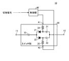
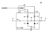
- FIG. 2 is a diagram illustrating a configuration of the switch device according to the first embodiment.
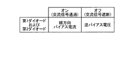
- FIG. 3 is a diagram illustrating a control operation of the switch device according to the first embodiment.
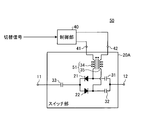
- FIG. 4 is a diagram illustrating a configuration of the switch device according to the second embodiment.
- FIG. 5 is a diagram illustrating functions of the switch device according to the third embodiment.
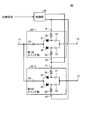
- FIG. 6 is a diagram illustrating a configuration of the switch device according to the third embodiment.
- FIG. 7 is a diagram illustrating functions of the switch device according to the fourth embodiment.
- FIG. 8 is a diagram illustrating the configuration of the switch device according to the fourth embodiment.
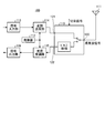
- FIG. 9 is a diagram illustrating a configuration of a wireless device according to the fifth embodiment.
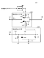
- FIG. 10 is a diagram illustrating a configuration of a switch device according to the fifth embodiment.
- FIG. 1 is a diagram illustrating functions of the switch device 10 according to the first embodiment.
- the switch device 10 is disposed on a transmission path between the first AC terminal 11 and the second AC terminal 12.
- the switch device 10 passes (ON) or blocks (OFF) an AC signal between the first AC terminal 11 and the second AC terminal 12 in accordance with a switching signal given from the outside. Note that the switch device 10 does not pass a DC signal between the first AC terminal 11 and the second AC terminal 12. Further, the AC signal may have any frequency.
- FIG. 2 is a diagram illustrating a configuration of the switch device 10 according to the first embodiment.
- the switch device 10 includes a switch unit 20 and a control unit 40.
- the switch unit 20 includes a first diode 21, a second diode 22, a first capacitor 31, a second capacitor 32, a third capacitor 33, a first inductor 34, and a second inductor 35.
- the first diode 21 and the second diode 22 have a rectifying function that allows a current in a direction from the anode to the cathode to pass therethrough and interrupts a current in the reverse direction.
- the first diode 21 and the second diode 22 may include devices other than the diodes as long as they have such a rectifying function.
- the first diode 21 and the second diode 22 are arranged in parallel in the opposite directions between the first AC terminal 11 and the second AC terminal 12.
- the cathode of the first diode 21 and the anode of the second diode 22 are on the first AC terminal 11 side
- the anode of the first diode 21 and the cathode of the second diode 22 are on the second AC terminal 12 side.
- the passage of the alternating current signal in the first embodiment means that the alternating current signal between the first alternating current terminal 11 and the second alternating current terminal 12 when the first diode 21 and the second diode 22 become conductive with respect to the alternating current signal.
- blocking of the alternating current signal in 1st Embodiment is the 1st diode 21 and the 2nd diode 22 becoming an open state with respect to an alternating current signal, between the 1st alternating current terminal 11 and the 2nd alternating current terminal 12. It means that the AC signal is cut off.
- first diode 21 and the second diode 22 are arranged in series in the forward direction between the first bias terminal 41 and the second bias terminal 42.
- the cathode of the first diode 21 is connected to the anode of the second diode 22, the anode of the first diode 21 is on the first bias terminal 41 side, and the cathode of the second diode 22 is on the second bias terminal 42 side.
- the first capacitor 31, the second capacitor 32, and the third capacitor 33 have a function of passing a signal in a band equal to or higher than the frequency of the input AC signal and blocking the DC voltage.
- the first capacitor 31, the second capacitor 32, and the third capacitor 33 may include devices other than capacitors as long as they have such a function.
- the first capacitor 31 is disposed between the second AC terminal 12 and the anode of the first diode 21.
- the first capacitor 31 has one end connected to the second AC terminal 12 and the other end connected to the anode of the first diode 21.
- the second capacitor 32 is disposed between the second AC terminal 12 and the cathode of the second diode 22.
- the second capacitor 32 has one end connected to the second AC terminal 12 and the other end connected to the cathode of the second diode 22.
- the third capacitor 33 is disposed between the first AC terminal 11 and the cathode of the first diode 21 (and the anode of the second diode 22).
- the third capacitor 33 has one end connected to the first AC terminal 11 and the other end connected to the cathode of the first diode 21 (and the anode of the second diode 22). Note that, when the connection point between the anode of the first diode 21 and the cathode of the second diode 22 is always at the ground potential, no DC voltage is applied to the first AC terminal 11. Therefore, in this case, the switch device 10 may be configured without the third capacitor 33.
- the first inductor 34 and the second inductor 35 have a function of passing a DC voltage and blocking a signal in a band equal to or higher than the frequency of the input AC signal.
- the first inductor 34 and the second inductor 35 may include devices other than the inductor as long as they have such a function.
- the first inductor 34 is disposed between the first bias terminal 41 and the anode of the first diode 21.
- the first inductor 34 has one end connected to the first bias terminal 41 and the other end connected to the anode of the first diode 21.
- the second inductor 35 is disposed between the second bias terminal 42 and the cathode of the second diode 22.
- the second inductor 35 has one end connected to the second bias terminal 42 and the other end connected to the cathode of the second diode 22.
- the control unit 40 switches the control voltage to be applied to the first bias terminal 41 and the second bias terminal 42 in accordance with a switching signal given from the outside.
- the controller 40 causes a forward bias current to flow through both the first diode 21 and the second diode 22 when conducting an AC signal. More specifically, the control unit 40 causes a forward bias current to flow through the first diode 21 and a forward bias current to the second diode 22 via the first diode 21 when conducting an AC signal. Therefore, a potential higher than the bias terminal 42 of the switch unit 20 is applied to the bias terminal 41.
- the applied control voltage is defined as a positive control voltage.
- the controller 40 is applied between the first bias terminal 41 and the second bias terminal 42 so that a forward bias current does not flow through the first diode 21 and the second diode 22 when the AC signal is released. Control voltage to be controlled.
- FIG. 3 is a diagram illustrating a control operation of the switch device 10 according to the first embodiment. Next, a specific operation of the switch device 10 will be described.
- the control unit 40 when the control unit 40 conducts an AC signal, the first bias terminal 41 is higher than the second bias terminal 42 so that a forward bias current flows through the second diode 22 via the first diode 21.
- Apply DC voltage For example, the control unit 40 applies a positive DC voltage to the first bias terminal 41 and applies a ground potential (reference potential) to the second bias terminal 42. Further, for example, the control unit 40 applies a positive DC voltage to the first bias terminal 41 and applies a negative DC voltage to the second bias terminal 42. For example, the control unit 40 applies a ground potential to the first bias terminal 41 and applies a negative DC voltage to the second bias terminal 42.
- the first bias terminal 41 passes through the first inductor 34, the first diode 21, the second diode 22, and the second inductor 35 to the second bias terminal 42.
- DC current flows. This current becomes a forward bias current of the first diode 21 and the second diode 22.
- the forward bias current is supplied in this way, the first diode 21 and the second diode 22 can conduct an AC signal.
- one component of the AC signal input from the first AC terminal 11 passes through the first diode 21 and is output from the second AC terminal 12. Further, the other component of the AC signal input from the first AC terminal 11 passes through the second diode 22 and is output from the second AC terminal 12.
- the control unit 40 applies a lower bias voltage to the first bias terminal 41 than the second bias terminal 42 so as to apply a reverse bias voltage to the first diode 21 and the second diode 22. Apply.
- the applied control voltage is defined as a negative control voltage.
- the control unit 40 applies a negative DC voltage to the first bias terminal 41 and applies a ground potential to the second bias terminal 42.
- the control unit 40 applies a negative DC voltage to the first bias terminal 41 and applies a positive DC voltage to the second bias terminal 42.
- the control unit 40 applies a ground potential to the first bias terminal 41 and applies a positive DC voltage to the second bias terminal 42.
- the control unit 40 may apply the same potential to the first bias terminal 41 and the second bias terminal 42 when the AC signal is released.
- the control unit 40 may apply a ground potential to the first bias terminal 41 and the second bias terminal 42.
- the control unit 40 may open the first bias terminal 41 and the second bias terminal 42 when releasing the AC signal. Even if it does in this way, if the voltage amplitude of an alternating current signal is smaller than the forward voltage which turns on the 1st diode 21 and the 2nd diode 22, the switch apparatus 10 can open
- an AC signal passes through two parallel paths of the first diode 21 and the second diode 22. Therefore, when passing a high power AC signal, the power of the signal passing through each of the first diode 21 and the second diode 22 is 1 ⁇ 2. Thereby, according to the switch apparatus 10, when passing a high electric power alternating current signal, a passage loss can be reduced.
- the switch device 10 may supply the forward bias current of one diode to the first diode 21 and the second diode 22. Thereby, according to the switch apparatus 10, an alternating current signal can be passed or interrupted with little electric power.
- the distortion that occurs when the AC signal passes through the diode is caused by the loss of current in the phase where the voltage of the AC signal becomes the reverse voltage of the diode.
- this distortion becomes large when an AC signal having a medium waveband having a longer period than the switching period of the diode is passed.
- the first diode 21 and the second diode 22 are arranged in parallel in opposite directions. Therefore, since the second diode 22 can pass a large current in a phase where the distortion is large in the first diode 21, the current loss in the first diode 21 is compensated by the second diode 22. On the other hand, in the phase where the distortion increases in the second diode 22, the first diode 21 can pass a large current, so that the current loss in the second diode 22 is compensated by the first diode 21. Therefore, according to the switch apparatus 10, distortion can be reduced over a wide band.
- the switch device 10 can pass and block a broadband AC signal with low power and small distortion. Thereby, according to the switch apparatus 10, selection etc. of the device which implement
- FIG. 4 is a diagram illustrating a configuration of the switch device 50 according to the second embodiment.
- the switch device 50 according to the second embodiment has substantially the same function and configuration as the switch device 10 according to the first embodiment. Accordingly, with regard to the switch device 50 according to the second embodiment, members having substantially the same functions as those in the first embodiment are denoted by the same reference numerals, and differences will be mainly described, and description of common points will be omitted. To do.
- the switch device 50 includes a switch unit 20A and a control unit 40.
- the switch unit 20 ⁇ / b> A includes a first inductor 34 and a second inductor 35 that are members of the switch unit 20 included in the switch device 10 according to the first embodiment, and a primary coil and a secondary coil wound around the core of one transformer 51.
- the configuration is a coil.
- the first inductor 34 and the second inductor 35 have the same number of turns.
- the first inductor 34 and the second inductor 35 are wound so that a reverse magnetic field is generated in the core when a forward bias current flows.
- the switch device 50 having such a configuration operates in the same manner as the switch device 10 according to the first embodiment, and has the same effects. Furthermore, since the switch device 50 includes the first inductor 34 and the second inductor 35 in one transformer 51, the number of components can be reduced.
- the switch device 50 can suppress the magnetic body constituting the transformer 51 from being magnetized or magnetically saturated by bringing the primary coil and the secondary coil into close contact with each other.
- the magnetic flux density generated by the AC signal is in the same phase in the primary coil and the secondary coil. Therefore, the first inductor 34 and the second inductor 35 have the same magnetic flux density when used alone and when used as the primary coil and secondary coil of the transformer 51. Therefore, the switch device 50 can set the volume of the magnetic body included in the transformer 51 to the volume of the magnetic body included in one single inductor. Therefore, according to the switch device 50, the volume of the transformer 51 can be reduced. In particular, when switching an AC signal in a relatively low frequency band such as a medium wave band, the parts are increased in size. Therefore, in such a case, the merit by including the first inductor 34 and the second inductor 35 in one transformer 51 is particularly great.
- FIG. 5 is a diagram illustrating functions of the switch device 60 according to the third embodiment.
- the switch device 60 allows an AC signal to pass between the first AC terminal 11 and the second AC terminal 12 in accordance with a switching signal given from outside (on), or the first AC terminal 11 and the third AC terminal. Whether to pass (turn on) the AC signal to / from the terminal 13 is switched.
- a path between the first AC terminal 11 and the second AC terminal 12 is a first conduction path
- a path between the first AC terminal 11 and the third AC terminal 13 is a second conduction path.
- the switch apparatus 60 interrupts
- the switching device 60 passes (turns on) the alternating current signal of the second conduction path
- the switching device 60 blocks (turns off) the alternating current signal of the first conduction path. That is, the switch device 60 constitutes an SPDT switch.
- FIG. 6 is a diagram illustrating a configuration of the switch device 60 according to the third embodiment.
- the switch device 60 includes a first switch unit 20-1, a second switch unit 20-2, and a control unit 40.
- the first switch unit 20-1 and the second switch unit 20-2 have the same configuration as the switch unit 20 included in the switch device 10 according to the first embodiment.
- the first switch unit 20-1 passes or blocks the AC signal of the first conduction path.
- the second switch unit 20-2 passes or blocks the AC signal of the second conduction path.
- the control unit 40 When the control unit 40 passes the AC signal of the first conduction path and blocks the AC signal of the second conduction path, the control unit 40 applies a forward bias to the first diode 21 and the second diode 22 of the first switch unit 20-1. A current is passed, and a reverse bias voltage is applied to the first diode 21 and the second diode 22 of the second switch unit 20-2. Conversely, when the control unit 40 blocks the AC signal on the first conduction path and passes the AC signal on the second conduction path, the control unit 40 causes the first diode 21 and the second diode 22 of the first switch unit 20-1 to A reverse bias voltage is applied to cause a forward bias current to flow through the first diode 21 and the second diode 22 of the second switch unit 20-2.
- control unit 40 may apply the same voltage to the first bias terminal 41 of the first switch unit 20-1 and the second bias terminal 42 of the second switch unit 20-2. Further, for example, the control unit 40 may apply the same voltage to the second bias terminal 42 of the first switch unit 20-1 and the first bias terminal 41 of the second switch unit 20-2.
- Such a switch device 60 is for switching between transmission and reception in a radio device or the like that is a wideband signal from, for example, a medium wave band to a short wave or VHF band and transmits / receives a relatively large power signal.
- a radio device or the like that is a wideband signal from, for example, a medium wave band to a short wave or VHF band and transmits / receives a relatively large power signal.
- the control unit 40 may apply a forward bias current or a reverse bias voltage to the first bias terminal 41 and the second bias terminal 42 of each switch unit as appropriate.
- first switch unit 20-1 and the second switch unit 20-2 may have the same configuration as the switch unit 20A included in the switch device 50 according to the second embodiment. Good.
- FIG. 7 is a diagram illustrating functions of the switch device 90 according to the fourth embodiment.
- the switch device 90 passes (turns on) an AC signal between the first AC terminal 14 and the second AC terminal 15 in accordance with a switching signal given from the outside, or the first AC terminal 14 and the second AC terminal.
- the AC signal between the terminals 15 is switched off (off).
- the passage of the AC signal in the fourth embodiment is a passage due to the opening of the switch device 90, and the interruption of the AC signal is performed by turning on the switch device 90, that is, by short-circuiting the AC signal to the ground potential.
- the switch device 90 connects the first AC terminal 14 and the second AC terminal 15 to the ground potential when the AC signal between the first AC terminal 14 and the second AC terminal 15 is cut off (off). To do. Further, when the switching device 90 allows an AC signal to pass between the first AC terminal 14 and the second AC terminal 15 (ON), the first AC terminal 14 and the second AC terminal 15 are opened from the ground potential. To do. That is, the switch device 90 passes or blocks an AC signal between the first AC terminal 14 and the second AC terminal 15 and the ground potential, that is, the ground.
- FIG. 8 is a diagram showing a configuration of the switch device 90 according to the fourth embodiment.
- the switch device 90 includes a switch unit 20B and a control unit 40.
- the switch unit 20B includes a first diode 21, a second diode 22, a sixth capacitor 91, a seventh capacitor 92, an eighth capacitor 93, a ninth capacitor 94, a first inductor 34, and a second inductor. 35.
- the first diode 21 and the second diode 22 are arranged in parallel in the opposite directions between the first AC terminal 14 and the second AC terminal 15 and the ground.
- the first diode 21 is arranged such that the anode is on the first AC terminal 14 and the second AC terminal 15 side, and the cathode is on the ground side.
- the second diode 22 is arranged such that the cathode is on the first AC terminal 14 and the second AC terminal 15 side and the anode is on the ground side.
- the passage of the AC signal in the fourth embodiment is a path between the first AC terminal 14 and the second AC terminal 15 when the first diode 21 and the second diode 22 are opened to the AC signal. It means that an AC signal is passed.
- blocking of the alternating current signal in 4th Embodiment is the 1st diode 21 and the 2nd diode 22 becoming a conduction
- the interruption in this case is an interruption due to a short circuit of the signal path.
- first diode 21 and the second diode 22 are arranged in series in the forward direction between the first bias terminal 41 and the second bias terminal 42.
- the anode of the second diode 22 is connected to the cathode of the first diode 21, the anode of the first diode 21 is on the first bias terminal 41 side, and the cathode of the second diode 22 is on the second bias terminal 42 side.
- the sixth capacitor 91, the seventh capacitor 92, the eighth capacitor 93, and the ninth capacitor 94 have a function of passing a signal in a band equal to or higher than the frequency of the input AC signal and blocking the DC voltage.
- the sixth capacitor 91, the seventh capacitor 92, the eighth capacitor 93, and the ninth capacitor 94 may include devices other than capacitors as long as they have such a function.
- the sixth capacitor 91 is disposed between the ground and the cathode of the first diode 21 (and the anode of the second diode 22).
- the sixth capacitor 91 has one end connected to the ground and the other end connected to the cathode of the first diode 21 (and the anode of the second diode 22).
- the seventh capacitor 92 is disposed between the anode of the first diode 21 and the cathode of the second diode 22.
- the seventh capacitor 92 has one end connected to the anode of the first diode 21 and the other end connected to the cathode of the second diode 22.
- the eighth capacitor 93 is disposed between the second AC terminal 15 and the cathode of the second diode 22.
- the eighth capacitor 93 has one end connected to the second AC terminal 15 and the other end connected to the cathode of the second diode 22.
- the ninth capacitor 94 is disposed between the first AC terminal 14 and the anode of the first diode 21.
- the ninth capacitor 94 has one end connected to the first AC terminal 14 and the other end connected to the anode of the first diode 21.
- the control unit 40 when passing an AC signal between the first AC terminal 14 and the second AC terminal 15, applies the first bias voltage to the first diode 21 and the second diode 22 so as to apply a reverse bias voltage. A DC voltage lower than that of the second bias terminal 42 is applied to the bias terminal 41.
- the control unit 40 causes the first bias current to flow to the second diode 22 via the first diode 21.
- a DC voltage higher than that of the second bias terminal 42 is applied to the bias terminal 41.
- the switch device 90 according to the present embodiment as described above can pass and block a broadband AC signal with a small amount of power and a small distortion, as in the first embodiment.
- FIG. 9 is a diagram illustrating a configuration of the wireless device 100 according to the fifth embodiment.
- Radio apparatus 100 includes a switching device 110, an antenna 111, an oscillator 112, a signal input unit 113, a modulation transmission unit 114, a reception demodulation unit 115, and a signal output unit 116.
- the switch device 110 is disposed on a transmission path between the first high frequency terminal 121 and the second high frequency terminal 122 and the common high frequency terminal 120.
- the switch device 110 passes a high-frequency signal between the first high-frequency terminal 121 and the common high-frequency terminal 120 when transmitting a signal. Further, when receiving a signal, the switch device 110 passes the high frequency signal between the second high frequency terminal 122 and the common high frequency terminal 120.
- the switch device 110 blocks the high-frequency signal between the second high-frequency terminal 122 and the common high-frequency terminal 120 when passing a high-frequency signal between the first high-frequency terminal 121 and the common high-frequency terminal 120.
- the switch device 110 blocks the high frequency signal between the first high frequency terminal 121 and the common high frequency terminal 120. That is, the switch device 110 constitutes an SPDT switch.
- the antenna 111 is connected to the common high frequency terminal 120 of the switch device 110.
- the antenna 111 radiates a high-frequency signal given from the common high-frequency terminal 120 to the space as a radio wave.
- the antenna 111 converts a radio wave in the space into a high-frequency signal and applies it to the common high-frequency terminal 120.
- the oscillator 112 outputs a carrier wave signal of a high frequency signal to be transmitted or received.
- the signal input unit 113 inputs a baseband signal such as an audio signal from the outside.
- the modulation transmission unit 114 modulates the baseband signal input by the signal input unit 113 into a carrier wave signal output by the oscillator 112 to generate a high frequency signal. Then, the modulation transmission unit 114 provides a high frequency signal to the first high frequency terminal 121 of the switch device 110 and transmits the high frequency signal from the antenna 111.
- the reception demodulation unit 115 receives the high frequency signal converted by the antenna 111 from the second high frequency terminal 122 of the switch device 110.
- the reception demodulation unit 115 demodulates the baseband signal from the received high frequency signal using the carrier wave signal output from the oscillator 112. Then, the reception demodulation unit 115 gives the demodulated baseband signal to the signal output unit 116.
- the signal output unit 116 outputs the baseband signal given from the reception demodulation unit 115 to the outside.
- FIG. 10 is a diagram illustrating a configuration of the switch device 110 according to the fifth embodiment.
- the switch device 110 includes a first switch unit 20C, a second switch unit 20D, and a control unit 40.
- the first switch unit 20C includes a first diode 21, a second diode 22, a first capacitor 31, a second capacitor 32, a third capacitor 33, a first inductor 34, and a phase shifter 145.
- the second switch unit 20 ⁇ / b> D includes a third diode 131, a fourth diode 132, a fourth capacitor 141, a fifth capacitor 142, a sixth capacitor 143, and a second inductor 35.
- the first diode 21, the second diode 22, the third diode 131, and the fourth diode 132 are, for example, PIN diodes.
- the first diode 21 and the second diode 22 are arranged in parallel in opposite directions to the conduction path of the high-frequency signal.
- the third diode 131 and the fourth diode 132 are arranged in parallel in opposite directions to the conduction path of the high-frequency signal.
- the first diode 21, the second diode 22, the third diode 131, and the fourth diode 132 are arranged in series in the forward direction between the first bias terminal 41 and the ground potential.
- the connection relationship between the first diode 21, the second diode 22, the first capacitor 31, the second capacitor 32, the third capacitor 33, and the first inductor 34 of the first switch unit 20C is the same as that of the switch unit 20 of the first embodiment.
- the first AC terminal 11 of the first embodiment is replaced with the first high-frequency terminal 121
- the second AC terminal 12 is replaced with the common high-frequency terminal 120
- the second inductor 35 is replaced with the phase shifter 145. Different.
- the connection relationship of the third diode 131, the fourth diode 132, the fourth capacitor 141, the fifth capacitor 142, and the sixth capacitor 143 of the second switch unit 20D is the same as the corresponding part of the switch unit 20B of the fourth embodiment.
- the second AC terminal 15 of the fourth embodiment is the second high-frequency terminal 122
- the second inductor 35 is connected to the ground instead of the control unit 40
- the location corresponding to the first AC terminal is the first switch unit 20C. It is connected to one end of the phase shifter 145, and is different in that there is no capacitor between one end of the phase shifter 145 and the diode 131.
- the fourth capacitor 141 is disposed between the ground and the cathode of the third diode 131. In the present embodiment, one end of the fourth capacitor 141 is connected to the ground, and the other end is connected to the cathode of the third diode 131.
- the fifth capacitor 142 is disposed between the anode of the third diode 131 and the cathode of the fourth diode 132.
- the fifth capacitor 142 has one end connected to the anode of the third diode 131 and the other end connected to the cathode of the fourth diode 132.
- the sixth capacitor 143 is disposed between the second high frequency terminal 122 and the cathode of the fourth diode 132.
- the sixth capacitor 143 has one end connected to the second high-frequency terminal 122 and the other end connected to the cathode of the fourth diode 132.
- the second inductor 35 is disposed between the cathode of the fourth diode 132 and the ground.
- the second inductor 35 has one end connected to the cathode of the fourth diode 132 and the other end connected to the ground.
- the phase shifter 145 of the first switch unit 20C delays the phase of the propagating high-frequency signal by 1 ⁇ 4 period. Therefore, when the high-frequency signal passes through the phase shifter 145, the phase of the high-frequency signal is delayed by 1 ⁇ 4 period. In addition, when one end of the phase shifter 145 is grounded at a high frequency, the other end has a high impedance. Therefore, the phase shifter 145 does not pass a signal from the other end when one end is set to a high-frequency ground potential. In order to conduct the direct current and delay the phase, a high-frequency line having an electrical length of 1 ⁇ 4 wavelength, such as a strip line or a coaxial cable, is used. Of course, the same effect can be obtained theoretically if it is not only a quarter wavelength but an odd multiple thereof.
- the phase shifter 145 is disposed between the cathode of the second diode 22 and the anode of the third diode 131.
- the phase shifter 145 has one end connected to the cathode of the second diode 22 and the other end connected to the anode of the third diode 131.
- the control unit 40 When transmitting a signal, that is, when allowing a high-frequency signal to pass between the first high-frequency terminal 121 and the common high-frequency terminal 120, the control unit 40 transmits from the first diode 21 to the second diode 22 of the first switch unit 20C. Further, a forward bias current flows from the second diode 22 of the first switch unit 20C to the third diode 131 of the second switch unit 20D via the phase shifter 145, and further from the third diode 131 to the fourth diode 132. A positive DC voltage is applied to the first bias terminal 41 so as to flow.
- control unit 40 applies a ground potential to the first bias terminal 41 when receiving a signal, that is, when passing a high-frequency signal between the common high-frequency terminal 120 and the second high-frequency terminal 122.
- a signal that is, when passing a high-frequency signal between the common high-frequency terminal 120 and the second high-frequency terminal 122.
- the control unit 40 controls the control voltage based on the switching signal from the control unit 40 using the ground side of the second inductor 35 as the second bias terminal 42. May be performed.
- the first inductor 34, the first diode 21, the second diode 22, the phase shifter 145, the third diode 131, the fourth diode 132, and the first bias terminal 41 A direct current flows through the second inductor 35 to the ground.
- This current becomes a forward bias current of the first diode 21 and the second diode 22.
- the forward bias current flows in this way, the first diode 21 and the second diode 22 are in a low impedance state and can conduct (turn on) the high-frequency signal.
- connection point a between the phase shifter 145 and the anode of the third diode 131 is conducted at a high frequency via the third diode 131 and the fourth capacitor 141, and is shorted to the ground.
- the phase shifter 145 does not affect the high-frequency signal transmitted between the first high-frequency terminal 121 and the common high-frequency terminal 120. Further, since the connection point a is short-circuited to the ground via the third diode 131, the fourth diode 132, and the fourth capacitor 141, it does not leak to the second high frequency terminal 122 side.
- the switch device 110 can pass a high-frequency signal between the first high-frequency terminal 121 and the common high-frequency terminal 120. Furthermore, when the high frequency signal is allowed to pass between the first high frequency terminal 121 and the common high frequency terminal 120, the switch device 110 can reliably isolate the second high frequency terminal 122 and the common high frequency terminal 120 from each other. .
- control unit 40 passes a high-frequency signal between the second high-frequency terminal 122 and the common high-frequency terminal 120 and blocks the high-frequency signal between the first high-frequency terminal 121 and the common high-frequency terminal 120, A ground potential is applied to the bias terminal 41.
- the first inductor 34, the first diode 21, the second diode 22, the phase shifter 145, the third diode 131, and the fourth diode 132 are connected from the first bias terminal 41.
- the path through the second inductor 35 becomes a ground potential in a direct current manner. Therefore, no forward bias current flows through the first diode 21, the second diode 22, the third diode 131, and the fourth diode 132. Accordingly, the first diode 21, the second diode 22, the third diode 131, and the fourth diode 132 release the high frequency signal.
- the high-frequency signal is blocked between the first high-frequency terminal 121 and the common high-frequency terminal 120 by the first diode 21 and the second diode 22. Further, the high-frequency signal is blocked by the third diode 131 and the fourth diode 132 in the path between the second high-frequency terminal 122 and the ground.
- the path output from the common high-frequency terminal 120 to the second high-frequency terminal 122 via the second capacitor 32, the phase shifter 145, the fifth capacitor 142, and the sixth capacitor 143 is any Since the diode is also in an open state, a high-frequency signal can be passed.
- the switch device 110 can pass a high-frequency signal between the second high-frequency terminal 122 and the common high-frequency terminal 120. Further, when the switch device 110 passes a high-frequency signal between the second high-frequency terminal 122 and the common high-frequency terminal 120, the switch device 110 is between the first high-frequency terminal 121 and the common high-frequency terminal 120, and between the common high-frequency terminal 120 and the ground. In addition, the second high frequency terminal 122 and the ground can be reliably isolated.
- the switch device 110 switches the path by four diodes. However, since the four diodes are connected in series, the forward bias current may be one current. Therefore, the switch device 110 can operate stably with a small amount of power.
Landscapes
- Engineering & Computer Science (AREA)
- Computer Networks & Wireless Communication (AREA)
- Signal Processing (AREA)
- Electronic Switches (AREA)
- Transceivers (AREA)
Abstract
広い帯域の交流信号を、少ない電力で小さい歪で通過または遮断する。交流信号を導通または開放するスイッチ部であって、交流信号の導通経路に対して相互に逆方向に配置された第1ダイオードおよび第2ダイオードを有し、順方向バイアス電流が、第1ダイオードを介して第2ダイオードに流れることにより交流信号を導通させ、順方向バイアス電流が、第1ダイオードおよび第2ダイオードに流れないことにより交流信号を開放することを特徴とする。
Description
本発明は、スイッチ部、スイッチ装置および無線機に関する。
受信時と送信時とでアンテナを共用する無線機は、送信時には送信機をアンテナ端子に接続し、受信時にはアンテナを受信機へ接続するスイッチ装置を備える。また、複数の周波数帯域の信号を送受信する無線機は、使用する周波数帯域に応じてフィルタおよび増幅回路等を切り替えるスイッチ装置を備える。
高周波信号のスイッチ装置として、例えば、ダイオードスイッチが知られている。このスイッチ装置は、高周波信号を通過させる場合にはダイオードに順方向電圧を印加して直流バイアス電流を流し、高周波信号を遮断する場合には電圧を印加せずに順方向バイアス電流を流さないようにする。
このようなスイッチ装置は、高電力の高周波信号を通過させる場合、ダイオードによる損失が増えて歪が発生する。この問題を解決するスイッチ装置として、同種の複数のダイオードを並列に接続したスイッチ装置が知られている。しかし、同種の複数のダイオードを並列に接続したスイッチ装置は、順方向バイアス電流が増加して電力消費が大きくなってしまう。また、このようなスイッチ装置は、順方向電圧の降下特性のばらつきにより、順方向バイアス電流のバランスが崩れて特性が悪化してしまう。
また、PIN(P-intrinsic-N)ダイオードを用いたスイッチ装置も知られている。PINダイオードを用いたスイッチ装置は、VHF(Very High Frequency)帯の信号の周期よりスイッチング速度が遅いので、VHF(Very High Frequency)帯以上の周波数の信号の通過時の歪が小さい。しかし、PINダイオードを用いたスイッチ装置は、中波帯等の周期の長い信号の通過時には、信号の周期よりスイッチング速度が速くなり歪が大きくなってしまう。従って、PINダイオードを用いたスイッチ装置は、例えば中波帯から短波またはVHF帯までの広帯域の信号をスイッチングしようとすると、通過時の歪を小さく且つ遮断時のアイソレーションを高くすることが難しい。
また、高周波信号用のSPDT(Single pole double throw)型のスイッチ装置は、高周波信号を遮断する方の経路をグランドに接続してアイソレーションを高くする。このようなスイッチ装置において、経路をグランドに接続する経路に複数のダイオードを並列に接続して、歪を小さくする回路が知られている。しかし、このようなスイッチ装置も、順方向バイアス電流が増加し、また、順方向電圧の降下特性のばらつきにより順方向バイアス電流のバランスが崩れて特性が悪化してしまう。
本発明は、上記に鑑みてなされたものであって、広い帯域の交流信号を、少ない電力且つ小さい歪で通過または遮断することができるスイッチ部、スイッチ装置および無線機を提供することを目的とする。
上述した課題を解決し、目的を達成するために、本発明に係るスイッチ部は、交流信号を導通または開放するスイッチ部であって、交流信号の導通経路に対して相互に逆方向に配置された第1ダイオードおよび第2ダイオードを備え、順方向バイアス電流の供給により、前記第1ダイオードを介して第2ダイオードに順方向バイアス電流を流して交流信号を導通させ、前記第1ダイオードおよび前記第2ダイオードに順方向バイアス電流を流さないことにより交流信号を開放することを特徴とする。
本発明によれば、広い帯域の交流信号を、少ない電力且つ小さい歪で通過または遮断することができる。
(第1実施形態)
図1は、第1実施形態に係るスイッチ装置10の機能を示す図である。スイッチ装置10は、第1交流端子11と第2交流端子12との間の伝送経路上に配置される。スイッチ装置10は、外部から与えられた切替信号に応じて、第1交流端子11と第2交流端子12との間の交流信号を通過(オン)または遮断(オフ)する。なお、スイッチ装置10は、第1交流端子11と第2交流端子12との間に直流信号を通過させない。また、交流信号は、どのような周波数であってもよい。
図1は、第1実施形態に係るスイッチ装置10の機能を示す図である。スイッチ装置10は、第1交流端子11と第2交流端子12との間の伝送経路上に配置される。スイッチ装置10は、外部から与えられた切替信号に応じて、第1交流端子11と第2交流端子12との間の交流信号を通過(オン)または遮断(オフ)する。なお、スイッチ装置10は、第1交流端子11と第2交流端子12との間に直流信号を通過させない。また、交流信号は、どのような周波数であってもよい。
図2は、第1実施形態に係るスイッチ装置10の構成を示す図である。スイッチ装置10は、スイッチ部20と、制御部40とを備える。スイッチ部20は、第1ダイオード21と、第2ダイオード22と、第1キャパシタ31と、第2キャパシタ32と、第3キャパシタ33と、第1インダクタ34と、第2インダクタ35とを有する。
第1ダイオード21および第2ダイオード22は、アノードからカソードに向かう方向の電流を通過させ、逆方向の電流を遮断する整流機能を有する。第1ダイオード21および第2ダイオード22は、このような整流機能を有すれば、ダイオード以外のデバイスを含んでもよい。
第1ダイオード21および第2ダイオード22は、第1交流端子11と第2交流端子12との間に互いに逆方向で並列に配置される。本実施形態では、第1ダイオード21のカソードおよび第2ダイオード22のアノードが第1交流端子11側となり、第1ダイオード21のアノードおよび第2ダイオード22のカソードが第2交流端子12側となるように、並列に配置される。つまり、第1ダイオード21のカソードおよび第2ダイオード22は、交流信号の導通経路に対して相互に逆方向に配置される。第1実施形態における交流信号の通過とは、第1ダイオード21および第2ダイオード22が交流信号に対して導通状態となることにより第1交流端子11と第2交流端子12との間に交流信号が通過されることを意味する。また、第1実施形態における交流信号の遮断とは、第1ダイオード21および第2ダイオード22が交流信号に対して開放状態となることにより第1交流端子11と第2交流端子12との間の交流信号が遮断されることを意味する。
また、第1ダイオード21および第2ダイオード22は、第1バイアス端子41と第2バイアス端子42との間に互いに順方向で直列に配置される。本実施形態では、第1ダイオード21のカソードが第2ダイオード22のアノードに接続され、第1ダイオード21のアノードが第1バイアス端子41側となり、第2ダイオード22のカソードが第2バイアス端子42側となるように、直列に配置される。
第1キャパシタ31、第2キャパシタ32および第3キャパシタ33は、入力される交流信号の周波数以上の帯域の信号を通過し、直流電圧を遮断する機能を有する。第1キャパシタ31、第2キャパシタ32および第3キャパシタ33は、このような機能を有すれば、キャパシタ以外のデバイスを含んでもよい。
第1キャパシタ31は、第2交流端子12と第1ダイオード21のアノードとの間に配置される。本実施形態では、第1キャパシタ31は、一方の端が第2交流端子12に接続され、他方の端が第1ダイオード21のアノードに接続される。
第2キャパシタ32は、第2交流端子12と第2ダイオード22のカソードとの間に配置される。本実施形態では、第2キャパシタ32は、一方の端が第2交流端子12に接続され、他方端が第2ダイオード22のカソードに接続される。
第3キャパシタ33は、第1交流端子11と、第1ダイオード21のカソード(および第2ダイオード22のアノード)との間に配置される。本実施形態では、第3キャパシタ33は、一方の端が第1交流端子11に接続され、他方の端が第1ダイオード21のカソード(および第2ダイオード22のアノード)に接続される。なお、第1ダイオード21のアノードと第2ダイオード22のカソードとの接続点が常にグランド電位である場合、第1交流端子11に直流電圧が印加されない。従って、この場合、スイッチ装置10は、第3キャパシタ33を備えない構成であってよい。
第1インダクタ34および第2インダクタ35は、直流電圧を通過し、入力される交流信号の周波数以上の帯域の信号を遮断する機能を有する。第1インダクタ34および第2インダクタ35は、このような機能を有すれば、インダクタ以外のデバイスを含んでもよい。
第1インダクタ34は、第1バイアス端子41と第1ダイオード21のアノードとの間に配置される。本実施形態では、第1インダクタ34は、一方の端が第1バイアス端子41に接続され、他方の端が第1ダイオード21のアノードに接続される。
第2インダクタ35は、第2バイアス端子42と第2ダイオード22のカソードとの間に配置される。本実施形態では、第2インダクタ35は、一方の端が第2バイアス端子42に接続され、他方の端が第2ダイオード22のカソードに接続される。
制御部40は、外部から与えられた切替信号に従って、第1バイアス端子41および第2バイアス端子42に印加する制御電圧を切り替える。制御部40は、交流信号を導通させる場合に、第1ダイオード21および第2ダイオード22の両者に順方向バイアス電流を流す。より具体的には、制御部40は、交流信号を導通させる場合に、第1ダイオード21に順方向バイアス電流を流すとともに、第1ダイオード21を介して第2ダイオード22に順方向バイアス電流を流すため、スイッチ部20のバイアス端子42より高い電位をバイアス端子41に印加する。この場合の印加する制御電圧を正の制御電圧と定義する。また、制御部40は、交流信号を開放する場合に第1ダイオード21および第2ダイオード22に順方向バイアス電流を流さないように、第1バイアス端子41と第2バイアス端子42との間に印加される制御電圧を制御する。
図3は、第1実施形態に係るスイッチ装置10の制御動作を示す図である。つぎに、スイッチ装置10の具体的な動作について説明する。
まず、制御部40は、交流信号を導通させる場合に、第1ダイオード21を介して第2ダイオード22に順方向バイアス電流を流すように、第1バイアス端子41に第2バイアス端子42よりも高い直流電圧を印加する。例えば、制御部40は、第1バイアス端子41に正の直流電圧を印加し、第2バイアス端子42にグランド電位(基準電位)を印加する。また、例えば、制御部40は、第1バイアス端子41に正の直流電圧を印加し、第2バイアス端子42に負の直流電圧を印加する。また、例えば、制御部40は、第1バイアス端子41にグランド電位を印加し、第2バイアス端子42に負の直流電圧を印加する。
このように正の制御電圧が印加された場合、第1バイアス端子41から、第1インダクタ34、第1ダイオード21、第2ダイオード22および第2インダクタ35を経由して、第2バイアス端子42に直流電流が流れる。この電流は、第1ダイオード21および第2ダイオード22の順方向バイアス電流となる。このように順方向バイアス電流が供給される場合、第1ダイオード21および第2ダイオード22は、交流信号を導通させることができる。
より具体的には、第1交流端子11から入力した交流信号の一方の成分は、第1ダイオード21を通過して、第2交流端子12から出力される。また、第1交流端子11から入力した交流信号の他方の成分は、第2ダイオード22を通過して、第2交流端子12から出力される。
一方、制御部40は、交流信号を開放する場合に、第1ダイオード21および第2ダイオード22に逆方向バイアス電圧を与えるように、第1バイアス端子41に第2バイアス端子42よりも低い直流電圧を印加する。この場合の印加する制御電圧を負の制御電圧と定義する。例えば、制御部40は、第1バイアス端子41に負の直流電圧を印加し、第2バイアス端子42にグランド電位を印加する。また、例えば、制御部40は、第1バイアス端子41に負の直流電圧を印加し、第2バイアス端子42に正の直流電圧を印加する。また、例えば、制御部40は、第1バイアス端子41にグランド電位を印加し、第2バイアス端子42に正の直流電圧を印加する。
このように負の制御電圧が印加された場合、第1ダイオード21および第2ダイオード22の整流特性により逆方向電流はほぼ流れず、第1ダイオード21および第2ダイオード22には逆方向バイアス電圧が与えられる。第1ダイオード21および第2ダイオード22は、逆方向バイアス電圧が与えられると、電極間容量が低下し、交流信号を開放する。より具体的には、第1交流端子11から入力した交流信号は、第1ダイオード21および第2ダイオード22により遮断されて第2交流端子12へは出力されない。
なお、制御部40は、交流信号を開放する場合に、第1バイアス端子41および第2バイアス端子42に同一電位を印加してもよい。例えば、制御部40は、第1バイアス端子41および第2バイアス端子42にグランド電位を印加してもよい。また、制御部40は、交流信号を開放する場合に、第1バイアス端子41および第2バイアス端子42を開放してもよい。このようにしても、スイッチ装置10は、交流信号の電圧振幅が、第1ダイオード21および第2ダイオード22がオンとなる順方向電圧より小さければ、交流信号を開放することができる。
以上のようなスイッチ装置10は、交流信号が第1ダイオード21および第2ダイオード22の2つの並列の経路を通過する。従って、高電力の交流信号を通過する場合、第1ダイオード21および第2ダイオード22のそれぞれを通過する信号の電力は1/2となる。これにより、スイッチ装置10によれば、高電力の交流信号を通過する場合に、通過損失を低減することができる。
さらに、第1ダイオード21および第2ダイオード22は、直流的に直列に接続されている。従って、スイッチ装置10は、第1ダイオード21および第2ダイオード22に1個分のダイオードの順方向バイアス電流を供給すればよい。これにより、スイッチ装置10によれば、少ない電力で交流信号の通過または遮断をすることができる。
また、交流信号がダイオードを通過する場合に生じる歪は、交流信号の電圧がダイオードの逆方向の電圧となる位相において、電流が損失することにより生じる。特に、この歪は、ダイオードのスイッチング期間より周期が長い中波帯の交流信号を通過させる場合に大きくなる。
しかし、第1ダイオード21および第2ダイオード22は、互いに逆方向に並列に配置されている。従って、第1ダイオード21において歪が大きくなる位相においては、第2ダイオード22が大きな電流を流すことができるので、第1ダイオード21での電流損失が第2ダイオード22により補われる。反対に、第2ダイオード22において歪が大きくなる位相においては、第1ダイオード21が大きな電流を流すことができるので、第2ダイオード22での電流損失が第1ダイオード21により補われる。従って、スイッチ装置10によれば、広帯域に亘り歪を小さくすることができる。
このように、スイッチ装置10は、広帯域の交流信号を少ない電力且つ小さい歪で通過および遮断することができる。これにより、スイッチ装置10によれば、第1ダイオード21および第2ダイオード22を実現するデバイスの選定等を容易とし、コストを小さくすることができる。
(第2実施形態)
図4は、第2実施形態に係るスイッチ装置50の構成を示す図である。第2実施形態に係るスイッチ装置50は、第1実施形態に係るスイッチ装置10と略同一の機能および構成を有する。従って、第2実施形態に係るスイッチ装置50については、第1実施形態と略同一の機能を有する部材には同一の符号を付け、相違点を中心に説明して、共通点については説明を省略する。
図4は、第2実施形態に係るスイッチ装置50の構成を示す図である。第2実施形態に係るスイッチ装置50は、第1実施形態に係るスイッチ装置10と略同一の機能および構成を有する。従って、第2実施形態に係るスイッチ装置50については、第1実施形態と略同一の機能を有する部材には同一の符号を付け、相違点を中心に説明して、共通点については説明を省略する。
スイッチ装置50は、スイッチ部20Aと、制御部40とを備える。スイッチ部20Aは、第1実施形態に係るスイッチ装置10が備えるスイッチ部20が有する部材である第1インダクタ34および第2インダクタ35を、1つのトランス51のコアに巻かれた一次コイルおよび二次コイルとした構成である。第1インダクタ34および第2インダクタ35は、同一の巻数を有する。また、第1インダクタ34および第2インダクタ35は、順方向バイアス電流が流された場合に、コアに逆方向の磁界が発生するように巻かれている。
このような構成のスイッチ装置50は、第1実施形態に係るスイッチ装置10と同一の動作をし、同一の作用効果を奏する。さらに、スイッチ装置50は、第1インダクタ34および第2インダクタ35を1つのトランス51に含めるので、部品点数を少なくすることができる。
また、第1インダクタ34および第2インダクタ35は、コアに逆方向の磁界を発生させて、コアの磁界を打ち消す。従って、スイッチ装置50は、一次コイルおよび二次コイルを密着させたり縒り合せたりすることにより、トランス51を構成する磁性体が磁化したり磁気飽和したりすることを抑制することができる。
また、トランス51は、交流信号により発生する磁束密度が一次コイルと二次コイルとで同位相となる。従って、第1インダクタ34および第2インダクタ35は、単体で使用される場合とトランス51の一次コイルおよび二次コイルとして使用される場合とで、磁束密度が同一となる。従って、スイッチ装置50は、トランス51に含まれる磁性体の体積を、1つのインダクタ単体に含まれる磁性体の体積とすることができる。よって、スイッチ装置50によれば、トランス51の体積を小さくすることができる。特に、中波帯のように比較的に低い周波数帯域の交流信号をスイッチングする場合、部品が大型化してしまう。従って、このような場合、特に、第1インダクタ34および第2インダクタ35を1つのトランス51に含めることによるメリットは大きい。
(第3実施形態)
図5は、第3実施形態に係るスイッチ装置60の機能を示す図である。スイッチ装置60は、外部から与えられた切替信号に応じて、第1交流端子11と第2交流端子12との間に交流信号を通過(オン)させるか、第1交流端子11と第3交流端子13との間の交流信号を通過(オン)させるかを切り替える。なお、第1交流端子11と第2交流端子12との間の経路とを第1導通経路とし、第1交流端子11と第3交流端子13との間の経路を第2導通経路とする。
図5は、第3実施形態に係るスイッチ装置60の機能を示す図である。スイッチ装置60は、外部から与えられた切替信号に応じて、第1交流端子11と第2交流端子12との間に交流信号を通過(オン)させるか、第1交流端子11と第3交流端子13との間の交流信号を通過(オン)させるかを切り替える。なお、第1交流端子11と第2交流端子12との間の経路とを第1導通経路とし、第1交流端子11と第3交流端子13との間の経路を第2導通経路とする。
なお、スイッチ装置60は、第1導通経路に交流信号を通過(オン)させる場合、第2導通経路の交流信号を遮断(オフ)する。スイッチ装置60は、第2導通経路の交流信号に通過(オン)させる場合、第1導通経路の交流信号を遮断(オフ)する。すなわち、スイッチ装置60は、SPDTスイッチを構成する。
図6は、第3実施形態に係るスイッチ装置60の構成を示す図である。スイッチ装置60は、第1のスイッチ部20-1と、第2のスイッチ部20-2と、制御部40とを備える。第1のスイッチ部20-1および第2のスイッチ部20-2は、第1実施形態に係るスイッチ装置10が備えるスイッチ部20と同一の構成を有する。
第1のスイッチ部20-1は、第1導通経路の交流信号を通過または遮断させる。第2のスイッチ部20-2は、第2導通経路の交流信号を通過または遮断させる。
制御部40は、第1導通経路の交流信号を通過させ、第2導通経路の交流信号を遮断させる場合、第1のスイッチ部20-1の第1ダイオード21および第2ダイオード22に順方向バイアス電流を流し、第2のスイッチ部20-2の第1ダイオード21および第2ダイオード22に逆方向バイアス電圧を与える。反対に、制御部40は、第1導通経路の交流信号を遮断させ、第2導通経路の交流信号を通過させる場合、第1のスイッチ部20-1の第1ダイオード21および第2ダイオード22に逆方向バイアス電圧を与えて、第2のスイッチ部20-2の第1ダイオード21および第2ダイオード22に順方向バイアス電流を流す。
例えば、制御部40は、第1のスイッチ部20-1の第1バイアス端子41と第2のスイッチ部20-2の第2バイアス端子42とに同一電圧を与えてもよい。また、例えば、制御部40は、第1のスイッチ部20-1の第2バイアス端子42と第2のスイッチ部20-2の第1バイアス端子41とに同一電圧を与えてもよい。
このようなスイッチ装置60は、例えば中波帯から短波またはVHF帯までの広帯域の信号であって、比較的に大きな電力の信号の送受信をする無線機等において、送信と受信との切り替え用とするだけでなく、3つ以上の複数のフィルタ回路を選択的に切り替える為に用いてもよい。その際、制御部40は、それぞれのスイッチ部の第1バイアス端子41および第2バイアス端子42に対し、順方向バイアス電流または逆方向バイアス電圧を、適時与えてもよい。
なお、第1のスイッチ部20-1および第2のスイッチ部20-2は、何れか一方または両者が、第2実施形態に係るスイッチ装置50が備えるスイッチ部20Aと同一の構成であってもよい。
(第4実施形態)
図7は、第4実施形態に係るスイッチ装置90の機能を示す図である。スイッチ装置90は、外部から与えられた切替信号に応じて、第1交流端子14と第2交流端子15との間に交流信号を通過(オン)させるか、第1交流端子14と第2交流端子15との間の交流信号を遮断(オフ)するかを切り替える。第4実施形態における交流信号の通過はスイッチ装置90の開放による通過であり、交流信号の遮断はスイッチ装置90を導通つまり交流信号を接地電位に短絡することにより行う。
図7は、第4実施形態に係るスイッチ装置90の機能を示す図である。スイッチ装置90は、外部から与えられた切替信号に応じて、第1交流端子14と第2交流端子15との間に交流信号を通過(オン)させるか、第1交流端子14と第2交流端子15との間の交流信号を遮断(オフ)するかを切り替える。第4実施形態における交流信号の通過はスイッチ装置90の開放による通過であり、交流信号の遮断はスイッチ装置90を導通つまり交流信号を接地電位に短絡することにより行う。
なお、スイッチ装置90は、第1交流端子14と第2交流端子15との間の交流信号を遮断(オフ)する場合には、第1交流端子14および第2交流端子15を接地電位に接続する。また、スイッチ装置90は、第1交流端子14と第2交流端子15との間に交流信号に通過(オン)させる場合には、第1交流端子14および第2交流端子15を接地電位から開放する。すなわち、スイッチ装置90は、第1交流端子14および第2交流端子15と、接地電位つまりグランドとの間の交流信号を通過または遮断する。
図8は、第4実施形態に係るスイッチ装置90の構成を示す図である。スイッチ装置90は、スイッチ部20Bと、制御部40とを有する。スイッチ部20Bは、第1ダイオード21と、第2ダイオード22と、第6キャパシタ91と、第7キャパシタ92と、第8キャパシタ93と、第9キャパシタ94と、第1インダクタ34と、第2インダクタ35とを有する。
第1ダイオード21および第2ダイオード22は、第1交流端子14および第2交流端子15と、グランドとの間に互いに逆方向で並列に配置される。本実施形態では、第1ダイオード21は、アノードが第1交流端子14および第2交流端子15側となり、カソードがグランド側となるように配置される。また、第2ダイオード22は、カソードが第1交流端子14および第2交流端子15側となり、アノードがグランド側となるように配置される。第4実施形態における交流信号の通過とは、第1ダイオード21および第2ダイオード22が交流信号に対して開放状態となることにより第1交流端子14と第2交流端子15との間の経路に交流信号が通過されることを意味する。また、第4実施形態における交流信号の遮断とは、第1ダイオード21および第2ダイオード22が交流信号に対して導通状態となることにより第1交流端子14と第2交流端子15との間の経路の交流信号が遮断されることを意味する。この場合の遮断は、信号経路の短絡による遮断である。
また、第1ダイオード21および第2ダイオード22は、第1バイアス端子41と第2バイアス端子42との間に互いに順方向で直列に配置される。本実施形態では、第2ダイオード22のアノードが第1ダイオード21のカソードに接続され、第1ダイオード21のアノードが第1バイアス端子41側となり、第2ダイオード22のカソードが第2バイアス端子42側となるように、直列に配置される。
第6キャパシタ91、第7キャパシタ92、第8キャパシタ93および第9キャパシタ94は、入力される交流信号の周波数以上の帯域の信号を通過し、直流電圧を遮断する機能を有する。第6キャパシタ91、第7キャパシタ92、第8キャパシタ93および第9キャパシタ94は、このような機能を有すれば、キャパシタ以外のデバイスを含んでもよい。
第6キャパシタ91は、グランドと、第1ダイオード21のカソード(および第2ダイオード22のアノード)との間に配置される。本実施形態では、第6キャパシタ91は、一方の端がグランドに接続され、他方の端が第1ダイオード21のカソード(および第2ダイオード22のアノード)に接続される。
第7キャパシタ92は、第1ダイオード21のアノードと第2ダイオード22のカソードとの間に配置される。本実施形態では、第7キャパシタ92は、一方の端が第1ダイオード21のアノードに接続され、他方の端が第2ダイオード22のカソードに接続される。
第8キャパシタ93は、第2交流端子15と第2ダイオード22のカソードとの間に配置される。本実施形態では、第8キャパシタ93は、一方の端が第2交流端子15に接続され、他方端が第2ダイオード22のカソードに接続される。
第9キャパシタ94は、第1交流端子14と、第1ダイオード21のアノードとの間に配置される。本実施形態では、第9キャパシタ94は、一方の端が第1交流端子14に接続され、他方の端が第1ダイオード21のアノードに接続される。
つぎに、スイッチ装置90の具体的な動作について説明する。まず、制御部40は、第1交流端子14と第2交流端子15との間に交流信号を通過させる場合、第1ダイオード21および第2ダイオード22に逆方向バイアス電圧を与えるように、第1バイアス端子41に第2バイアス端子42よりも低い直流電圧を印加する。
このように逆方向の直流電圧が印加された場合、第1ダイオード21および第2ダイオード22には逆方向バイアス電圧が与えられる。従って、第1交流端子14から入力した交流信号は、グランドに流れずに、第2交流端子15へ出力される。
制御部40は、第1交流端子14と第2交流端子15との間の交流信号を遮断する場合、第1ダイオード21を介して第2ダイオード22に順方向バイアス電流を流すように、第1バイアス端子41に第2バイアス端子42よりも高い直流電圧を印加する。
このように順方向の直流電圧が印加された場合、第1ダイオード21および第2ダイオード22は、順方向バイアス電流が流れ、交流信号を導通させることができる。従って、第1交流端子14から入力した交流信号は、グランドへと流れて、第2交流端子15へは出力されない。
以上のような本実施形態に係るスイッチ装置90は、第1実施形態と同様に、広帯域の交流信号を少ない電力且つ小さい歪で通過および遮断することができる。
(第5実施形態)
図9は、第5実施形態に係る無線機100の構成を示す図である。無線機100は、スイッチ装置110と、アンテナ111と、発振器112と、信号入力部113と、変調送信部114と、受信復調部115と、信号出力部116とを備える。
図9は、第5実施形態に係る無線機100の構成を示す図である。無線機100は、スイッチ装置110と、アンテナ111と、発振器112と、信号入力部113と、変調送信部114と、受信復調部115と、信号出力部116とを備える。
スイッチ装置110は、第1高周波端子121および第2高周波端子122と共通高周波端子120との間の伝送経路上に配置される。スイッチ装置110は、信号を送信する場合には、第1高周波端子121と共通高周波端子120との間に高周波信号を通過させる。また、スイッチ装置110は、信号を受信する場合には、第2高周波端子122と共通高周波端子120との間に高周波信号を通過させる。
なお、スイッチ装置110は、第1高周波端子121と共通高周波端子120との間に高周波信号を通過させる場合には、第2高周波端子122と共通高周波端子120との間の高周波信号を遮断する。また、スイッチ装置110は、第2高周波端子122と共通高周波端子120との間に高周波信号を通過させる場合には、第1高周波端子121と共通高周波端子120との間の高周波信号を遮断する。すなわち、スイッチ装置110は、SPDTスイッチを構成する。
アンテナ111は、スイッチ装置110の共通高周波端子120と接続される。アンテナ111は、信号を送信する場合には、共通高周波端子120から与えられた高周波信号を電波として空間に放射する。また、アンテナ111は、信号を受信する場合には、空間の電波を高周波信号に変換して共通高周波端子120へと与える。
発振器112は、送信または受信する高周波信号の搬送波信号を出力する。信号入力部113は、例えば音声信号等のベースバンド信号を外部から入力する。変調送信部114は、信号入力部113が入力したベースバンド信号を、発振器112が出力した搬送波信号に変調して高周波信号を生成する。そして、変調送信部114は、スイッチ装置110の第1高周波端子121へと高周波信号を与えて、アンテナ111から高周波信号を送信する。
受信復調部115は、スイッチ装置110の第2高周波端子122から、アンテナ111により変換された高周波信号を受信する。受信復調部115は、発振器112が出力した搬送波信号を用いて、受信した高周波信号からベースバンド信号を復調する。そして、受信復調部115は、復調したベースバンド信号を信号出力部116に与える。信号出力部116は、受信復調部115から与えられたベースバンド信号を外部へと出力する。
図10は、第5実施形態に係るスイッチ装置110の構成を示す図である。スイッチ装置110は、第1のスイッチ部20Cと、第2のスイッチ部20Dと、制御部40とを備える。第1のスイッチ部20Cは、第1ダイオード21と、第2ダイオード22と、第1キャパシタ31と、第2キャパシタ32と、第3キャパシタ33と、第1インダクタ34と、移相器145とを有する。第2のスイッチ部20Dは、第3ダイオード131と、第4ダイオード132と、第4キャパシタ141と、第5キャパシタ142と、第6キャパシタ143と、第2インダクタ35とを有する。
本実施形態では、第1ダイオード21、第2ダイオード22、第3ダイオード131および第4ダイオード132は、例えば、PINダイオードである。
第1ダイオード21および第2ダイオード22は、高周波信号の導通経路に対し互いに逆方向で並列に配置される。第3ダイオード131および第4ダイオード132は、高周波信号の導通経路に対し互いに逆方向で並列に配置される。また、第1ダイオード21、第2ダイオード22、第3ダイオード131および第4ダイオード132は、第1バイアス端子41と接地電位との間に互いに順方向で直列に配置される。
第1のスイッチ部20Cの、第1ダイオード21、第2ダイオード22、第1キャパシタ31、第2キャパシタ32、第3キャパシタ33および第1インダクタ34の接続関係が第1実施形態のスイッチ部20と同一であるが、第1実施形態の第1交流端子11が第1高周波端子121に、第2交流端子12が共通高周波端子120に、第2インダクタ35が移相器145に置き換わっている点において異なる。
第2のスイッチ部20Dの、第3ダイオード131、第4ダイオード132、第4キャパシタ141、第5キャパシタ142および第6キャパシタ143の接続関係は、第4実施形態のスイッチ部20Bの該当箇所と同一であるが、第4実施形態の第2交流端子15が第2高周波端子122となり、第2インダクタ35が制御部40ではなくグランドに接続され、第1交流端子にあたる箇所が第1スイッチ部20Cの移相器145の一端に接続され、移相器145の一端とダイオード131との間にキャパシタは存在しない点が異なる。
第2のスイッチ部20Dの接続をより具体的に説明する。第4キャパシタ141は、グランドと第3ダイオード131のカソードとの間に配置される。本実施形態では、第4キャパシタ141は、一方の端がグランドに接続され、他方の端が第3ダイオード131のカソードに接続される。
第5キャパシタ142は、第3ダイオード131のアノードと第4ダイオード132のカソードとの間に配置される。本実施形態では、第5キャパシタ142は、一方の端が第3ダイオード131のアノードに接続され、他方の端が第4ダイオード132のカソードに接続される。
第6キャパシタ143は、第2高周波端子122と第4ダイオード132のカソードとの間に配置される。本実施形態では、第6キャパシタ143は、一方の端が第2高周波端子122に接続され、他方の端が第4ダイオード132のカソードに接続される。
第2インダクタ35は、第4ダイオード132のカソードとグランドとの間に配置される。本実施形態では、第2インダクタ35は、一方の端が第4ダイオード132のカソードに接続され、他方の端がグランドに接続される。
第1のスイッチ部20Cの移相器145は、伝搬する高周波信号の位相を1/4周期遅延させる。従って、高周波信号が移相器145を通過した場合、高周波信号の位相は1/4周期遅延する。また、移相器145は、一方の端が高周波的に接地電位とされた場合、他方の端は高インピーダンスとなる。従って、移相器145は、一方の端が高周波的なグランド電位とされた場合、他方の端から信号を通過させない。直流を導通し位相を遅延させるため、電気長が1/4波長の高周波線路たとえばストリップラインや同軸ケーブルが用いられる。むろん1/4波長だけでなく、その奇数倍であれば理論的には同様の効果が得られる。
移相器145は、第2ダイオード22のカソードと第3ダイオード131のアノードとの間に配置される。本実施形態では、移相器145は、一方の端が第2ダイオード22のカソードに接続され、他方の端が第3ダイオード131のアノードに接続される。
制御部40は、信号を送信する場合、すなわち、第1高周波端子121と共通高周波端子120との間に高周波信号を通過させる場合、第1のスイッチ部20Cの第1ダイオード21から第2ダイオード22、さらには第1のスイッチ部20Cの第2ダイオード22から移相器145を介して第2のスイッチ部20Dの第3ダイオード131、またさらに第3ダイオード131から第4ダイオード132に順方向バイアス電流を流すように、第1バイアス端子41に正の直流電圧を印加する。また、制御部40は、信号を受信する場合、すなわち、共通高周波端子120と第2高周波端子122との間に高周波信号を通過させる場合、第1バイアス端子41にグランド電位を印加する。本実施形態ではバイアス電流を流す経路は1つでありバイアス端子は1つであるが、第2インダクタ35のグランド側を第2バイアス端子42として制御部40より切替信号に基づいて制御電圧の制御を行ってもよい。
つぎに、スイッチ装置110の具体的な動作について説明する。まず、制御部40は、第1高周波端子121と共通高周波端子120との間に高周波信号を通過させ、第2高周波端子122と共通高周波端子120との間の高周波信号を遮断する場合、第1バイアス端子41に正の制御電圧を印加する。
このように正の制御電圧が印加された場合、第1バイアス端子41から、第1インダクタ34、第1ダイオード21、第2ダイオード22、移相器145、第3ダイオード131、第4ダイオード132および第2インダクタ35を経由して、グランドに直流電流が流れる。この電流は、第1ダイオード21および第2ダイオード22の順方向バイアス電流となる。このように順方向バイアス電流が流れる場合、第1ダイオード21および第2ダイオード22は、低インピーダンス状態となり高周波信号を導通(オン)させることができる。
この状態で第1高周波端子121に高周波信号が入力された場合、入力された高周波信号の一方の成分は、第3キャパシタ33、第1ダイオード21および第1キャパシタ31を通過して、共通高周波端子120から出力される。また、第1高周波端子121から入力した高周波信号のもう一方の成分は、第3キャパシタ33、第2ダイオード22および第2キャパシタ32を通過して、共通高周波端子120から出力される。
また、第3ダイオード131および第4ダイオード132にも順方向バイアス電流が流れる。従って、第3ダイオード131および第4ダイオード132も低インピーダンス状態となる。これにより、移相器145と第3ダイオード131のアノードとの接続点aは、第3ダイオード131および第4キャパシタ141を経由して高周波的に導通し、グランドにショートされる。移相器145は、一方の端(接続点a)が高周波的にグランドにショートされると、他方の端(第2ダイオード22のカソードに接続された端)は、高インピーダンス状態となる。従って、移相器145は、第1高周波端子121と共通高周波端子120との間を伝送する高周波信号に対して影響を与えない。また、接続点aが第3ダイオード131、第4ダイオード132および第4キャパシタ141を経由してグランドにショートされているので、第2高周波端子122側へは漏れ出ない。
このように、スイッチ装置110は、第1高周波端子121と共通高周波端子120との間に高周波信号を通過させることができる。さらに、スイッチ装置110は、第1高周波端子121と共通高周波端子120との間に高周波信号を通過させる場合、第2高周波端子122と共通高周波端子120との間を確実にアイソレーションすることができる。
一方、制御部40は、第2高周波端子122と共通高周波端子120との間に高周波信号に通過させ、第1高周波端子121と共通高周波端子120との間の高周波信号を遮断する場合、第1バイアス端子41にグランド電位を印加する。
第1バイアス端子41にグランド電位が印加されると、第1バイアス端子41から、第1インダクタ34、第1ダイオード21、第2ダイオード22、移相器145、第3ダイオード131、第4ダイオード132および第2インダクタ35を経由した経路が直流的にグランド電位となる。従って、第1ダイオード21、第2ダイオード22、第3ダイオード131および第4ダイオード132には、順方向バイアス電流が流れない。従って、第1ダイオード21、第2ダイオード22、第3ダイオード131および第4ダイオード132は、高周波信号を開放する。
このため、第1高周波端子121と共通高周波端子120との間は、第1ダイオード21および第2ダイオード22により高周波信号が遮断される。また、第2高周波端子122とグランドとの間の経路は、第3ダイオード131および第4ダイオード132により高周波信号が遮断される。
これに対して、共通高周波端子120から、第2キャパシタ32、移相器145、第5キャパシタ142および第6キャパシタ143を経由して、第2高周波端子122へと出力される経路は、何れのダイオードも開放状態なので、高周波信号を通過させることができる。
このように、スイッチ装置110は、第2高周波端子122と共通高周波端子120との間に高周波信号を通過させることができる。さらに、スイッチ装置110は、第2高周波端子122と共通高周波端子120との間に高周波信号を通過させる場合、第1高周波端子121と共通高周波端子120との間、共通高周波端子120とグランドの間、および、第2高周波端子122とグランドの間を、確実にアイソレーションすることができる。
また、スイッチ装置110は、4つのダイオードにより経路を切り替えるが、4つのダイオードは直列に接続されているので、順方向バイアス電流は1個分の電流でよい。従って、スイッチ装置110は、少ない電力で安定した動作をすることができる。
以上の実施形態は、例として提示したものであり、発明の範囲を限定することは意図していない。これら新規な実施形態は、その他の様々な形態で実施されることが可能であり、発明の要旨を逸脱しない範囲で、種々の省略、置き換え、変更を行うことができる。
10,50,60,90,110 スイッチ装置
20,20A,20B スイッチ部
20-1,20C 第1のスイッチ部
20-2,20D 第2のスイッチ部
21 第1ダイオード
22 第2ダイオード
31 第1キャパシタ
32 第2キャパシタ
33 第3キャパシタ
34 第1インダクタ
35 第2インダクタ
40 制御部
51 トランス
61 第3ダイオード
62 第4キャパシタ
63 第5キャパシタ
64 第3インダクタ
65 第4インダクタ
91 第6キャパシタ
92 第7キャパシタ
93 第8キャパシタ
94 第9キャパシタ
100 無線機
131 第3ダイオード
132 第4ダイオード
141 第4キャパシタ
142 第5キャパシタ
143 第6キャパシタ
145 移相器
20,20A,20B スイッチ部
20-1,20C 第1のスイッチ部
20-2,20D 第2のスイッチ部
21 第1ダイオード
22 第2ダイオード
31 第1キャパシタ
32 第2キャパシタ
33 第3キャパシタ
34 第1インダクタ
35 第2インダクタ
40 制御部
51 トランス
61 第3ダイオード
62 第4キャパシタ
63 第5キャパシタ
64 第3インダクタ
65 第4インダクタ
91 第6キャパシタ
92 第7キャパシタ
93 第8キャパシタ
94 第9キャパシタ
100 無線機
131 第3ダイオード
132 第4ダイオード
141 第4キャパシタ
142 第5キャパシタ
143 第6キャパシタ
145 移相器
Claims (11)
- 交流信号を導通または開放するスイッチ部であって、
交流信号の導通経路に対して相互に逆方向に配置された第1ダイオードおよび第2ダイオードと、を備え、
順方向バイアス電流の供給により、前記第1ダイオードを介して第2ダイオードに順方向バイアス電流を流して交流信号を導通させ、
前記第1ダイオードおよび前記第2ダイオードに順方向バイアス電流を流さないことにより交流信号を開放すること、
を特徴とするスイッチ部。 - 請求項1に記載のスイッチ部を備えたスイッチ装置であって、
前記スイッチ部を導通させる際に順方向バイアス電流を供給し、前記スイッチ部を開放させる際に順方向バイアス電流を流さないように制御する、もしくは逆方向バイアス電圧を印加するよう制御する制御部を備えることを特徴とするスイッチ装置。 - 請求項1に記載のスイッチ部を複数備えたスイッチ装置であって、
前記複数のスイッチ部を選択的に導通させる際に順方向バイアス電流を供給し、前記複数のスイッチ部を選択的に開放させる際に、順方向バイアス電流を流さないように制御する、もしくは逆方向バイアス電圧を印加するよう制御する制御部を備えること、
を特徴とするスイッチ装置。 - 第1交流端子と第2交流端子との2つの交流端子をさらに備え、
前記スイッチ部は、前記第1交流端子と前記第2交流端子との間の伝送経路上に配置され、交流信号を導通させることにより前記伝送経路を通過させ、交流信号を開放させることにより前記伝送経路を遮断することを特徴とする請求項2に記載のスイッチ装置。 - 第1交流端子と第2交流端子との2つの交流端子をさらに備え、
前記スイッチ部は、前記第1交流端子と前記第2交流端子との間の伝送経路上と、接地電位との間に配置され、交流信号を開放することにより前記伝送経路を通過させ、交流信号を導通することにより前記伝送経路を短絡して遮断することを特徴とする請求項2に記載のスイッチ装置。 - 前記スイッチ部は、
前記第2交流端子と前記第1ダイオードのアノードとの間に配置された第1キャパシタと、
前記第2交流端子と前記第2ダイオードのカソードとの間に配置された第2キャパシタと、
前記第1ダイオードのアノードに接続され前記制御部からのバイアス電流を供給する第1インダクタと、
前記第2のダイオードのカソードに接続され前記制御部からのバイアス電流を供給する第2インダクタと、
をさらに有し、
前記第2ダイオードのアノードは、前記第1ダイオードのカソードに接続されること、
を特徴とする請求項4に記載のスイッチ装置。 - 前記スイッチ部は、前記第1交流端子と前記第1ダイオードのカソードとの間に配置された第3キャパシタをさらに有すること、
を特徴とする請求項5に記載のスイッチ装置。 - 前記スイッチ部は、
前記第1交流端子と前記第1ダイオードのアノードとの間に配置された第1キャパシタと、
前記第2交流端子と前記第2ダイオードのカソードとの間に配置された第2キャパシタと、
前記第1ダイオードのアノードと前記第2ダイオードのカソード間に配置された第3キャパシタと、
前記第1ダイオードのアノードに接続され前記制御部からのバイアス電流を供給する第1インダクタと、
前記第2のダイオードのカソードに接続され前記制御部からのバイアス電流を供給する第2インダクタと、
前記第2ダイオードのアノードと前記第1ダイオードのカソードとが接続され、その接続箇所と、接地電位との間に配置された第4のキャパシタとを有すること、
を特徴とする請求項5に記載のスイッチ装置。 - 前記第1インダクタおよび前記第2インダクタは、トランスの一次コイルおよび二次コイルであり、順方向バイアス電流が流された場合にコアに逆方向の磁界が発生するように巻かれている
請求項6から8の何れか1項に記載のスイッチ装置。 - 共通高周波端子と第1高周波端子との間の第1伝送経路に高周波信号を通過させるか、前記共通高周波端子と第2高周波端子との間の第2伝送経路に高周波信号を通過させるかを切り替えるスイッチ装置であって、
前記第1伝送経路に対して相互に逆方向に配置された第1ダイオードおよび第2ダイオードと、
前記第2高周波端子と接地電位の間に対して相互に逆方向に配置された第3ダイオードおよび第4ダイオードと、
前記共通高周波端子と前記第3ダイオードとの間に、高周波信号の波長の1/4の奇数倍にあたる電気長を備えた移相器と、
前記第1ダイオード、前記第2ダイオード、前記移相器、前記第3ダイオード、そして前記第4ダイオードを経由した経路に順方向バイアス電流を流すことにより、
前記第1ダイオードおよび前記第2ダイオードを導通させ、前記第1伝送経路に高周波信号の通過を可とさせるとともに、前記第3ダイオードおよび前記第4ダイオードを導通させ前記第2高周波端子を接地電位に短絡することにより前記第2伝送経路の高周波信号の通過を不可とし、
前記順方向バイアス電流を流さないことにより、
前記第1ダイオードおよび前記第2ダイオードを開放させ、前記第1伝送経路に高周波信号の通過を不可とさせるとともに、前記第3ダイオードおよび前記第4ダイオードを開放させ前記第2高周波端子と接地電位との間を開放し前記第2伝送経路の高周波信号の通過を可とするように制御する制御部と、
を備えるスイッチ装置。 - 請求項10に記載のスイッチ装置と、
前記スイッチ装置の前記共通高周波端子と接続されたアンテナと、
前記スイッチ装置の前記第1高周波端子と接続された変調送信部と、
前記スイッチ装置の前記第2高周波端子と接続された受信復調部と、
を備え、
前記スイッチ装置は、送信する場合には、前記第1高周波端子と前記共通高周波端子との間の高周波信号の通過を可とさせ、信号を受信する場合には、前記第2高周波端子と前記共通高周波端子との間の高周波信号の通過を可とさせる
無線機。
Applications Claiming Priority (2)
| Application Number | Priority Date | Filing Date | Title |
|---|---|---|---|
| JP2015-082441 | 2015-04-14 | ||
| JP2015082441A JP2018093254A (ja) | 2015-04-14 | 2015-04-14 | スイッチ部、スイッチ装置および無線機 |
Publications (1)
| Publication Number | Publication Date |
|---|---|
| WO2016167096A1 true WO2016167096A1 (ja) | 2016-10-20 |
Family
ID=57126488
Family Applications (1)
| Application Number | Title | Priority Date | Filing Date |
|---|---|---|---|
| PCT/JP2016/059448 Ceased WO2016167096A1 (ja) | 2015-04-14 | 2016-03-24 | スイッチ部、スイッチ装置および無線機 |
Country Status (2)
| Country | Link |
|---|---|
| JP (1) | JP2018093254A (ja) |
| WO (1) | WO2016167096A1 (ja) |
Citations (5)
| Publication number | Priority date | Publication date | Assignee | Title |
|---|---|---|---|---|
| JPS51120163A (en) * | 1975-04-15 | 1976-10-21 | Fujitsu Ltd | Diode switch circuit |
| JPS5933936A (ja) * | 1982-08-19 | 1984-02-24 | Pioneer Electronic Corp | 送受信切換回路 |
| JPS6118639U (ja) * | 1984-07-06 | 1986-02-03 | ソニー株式会社 | スイツチ回路 |
| JPH06169243A (ja) * | 1992-11-30 | 1994-06-14 | Ando Electric Co Ltd | スイッチング回路 |
| JP2001148609A (ja) * | 1999-11-19 | 2001-05-29 | Kojima Press Co Ltd | アンテナ、平衡不平衡変換器および受信機 |
-
2015
- 2015-04-14 JP JP2015082441A patent/JP2018093254A/ja active Pending
-
2016
- 2016-03-24 WO PCT/JP2016/059448 patent/WO2016167096A1/ja not_active Ceased
Patent Citations (5)
| Publication number | Priority date | Publication date | Assignee | Title |
|---|---|---|---|---|
| JPS51120163A (en) * | 1975-04-15 | 1976-10-21 | Fujitsu Ltd | Diode switch circuit |
| JPS5933936A (ja) * | 1982-08-19 | 1984-02-24 | Pioneer Electronic Corp | 送受信切換回路 |
| JPS6118639U (ja) * | 1984-07-06 | 1986-02-03 | ソニー株式会社 | スイツチ回路 |
| JPH06169243A (ja) * | 1992-11-30 | 1994-06-14 | Ando Electric Co Ltd | スイッチング回路 |
| JP2001148609A (ja) * | 1999-11-19 | 2001-05-29 | Kojima Press Co Ltd | アンテナ、平衡不平衡変換器および受信機 |
Also Published As
| Publication number | Publication date |
|---|---|
| JP2018093254A (ja) | 2018-06-14 |
Similar Documents
| Publication | Publication Date | Title |
|---|---|---|
| JP6721472B2 (ja) | 受信回路、無線通信モジュール、無線通信装置 | |
| WO2012165241A1 (ja) | 高周波スイッチ | |
| JP5075958B2 (ja) | 高周波スイッチ回路および無線通信装置 | |
| US20160248470A1 (en) | Transmitter/receiver apparatus, transmitter apparatus and transmitting/receiving method | |
| JP2015226313A (ja) | スイッチ回路付き利得可変型増幅器 | |
| KR100848261B1 (ko) | Rf 스위치 및 rf 스위치를 포함하는 장치 | |
| US8970445B2 (en) | Radio device | |
| US9966987B2 (en) | Radio frequency switching system | |
| US20230086793A1 (en) | Radio frequency module and communication device | |
| JP2011155357A (ja) | マルチバンド電力増幅器 | |
| JP2017135619A (ja) | スイッチ部、スイッチ装置および無線機 | |
| WO2016167096A1 (ja) | スイッチ部、スイッチ装置および無線機 | |
| US11894619B2 (en) | Passive vector modulator | |
| JP5610787B2 (ja) | 高周波スイッチ回路 | |
| WO2011118020A1 (ja) | 受信装置 | |
| KR101175898B1 (ko) | Rf 안테나 스위치 회로, 고주파 안테나 부품 및 이동통신기기 | |
| JP6466872B2 (ja) | 通信回路 | |
| CN105450190B (zh) | 单端与推挽双结构的电子管功放电路 | |
| JP4213706B2 (ja) | 高周波スイッチ回路 | |
| JP2015073301A (ja) | 高周波スイッチ回路 | |
| JP2013236145A (ja) | 送信ダイバーシティ高周波回路及びダ送信方法 | |
| JP2012239011A (ja) | 高周波スイッチ | |
| US20100267349A1 (en) | Apparatus and method for isolation and power handling in a radio frequency switch | |
| WO2024164668A1 (zh) | 射频模块、天线装置和通信设备 | |
| WO2022259442A1 (ja) | 高周波スイッチ |
Legal Events
| Date | Code | Title | Description |
|---|---|---|---|
| 121 | Ep: the epo has been informed by wipo that ep was designated in this application |
Ref document number: 16779887 Country of ref document: EP Kind code of ref document: A1 |
|
| NENP | Non-entry into the national phase |
Ref country code: DE |
|
| 122 | Ep: pct application non-entry in european phase |
Ref document number: 16779887 Country of ref document: EP Kind code of ref document: A1 |
|
| NENP | Non-entry into the national phase |
Ref country code: JP |