WO2016152811A1 - Waveguide tube/transmission line converter and antenna device - Google Patents
Waveguide tube/transmission line converter and antenna device Download PDFInfo
- Publication number
- WO2016152811A1 WO2016152811A1 PCT/JP2016/058847 JP2016058847W WO2016152811A1 WO 2016152811 A1 WO2016152811 A1 WO 2016152811A1 JP 2016058847 W JP2016058847 W JP 2016058847W WO 2016152811 A1 WO2016152811 A1 WO 2016152811A1
- Authority
- WO
- WIPO (PCT)
- Prior art keywords
- waveguide
- transmission line
- dielectric substrate
- line converter
- antenna elements
- Prior art date
Links
Images


Classifications
-
- H—ELECTRICITY
- H01—ELECTRIC ELEMENTS
- H01P—WAVEGUIDES; RESONATORS, LINES, OR OTHER DEVICES OF THE WAVEGUIDE TYPE
- H01P5/00—Coupling devices of the waveguide type
- H01P5/08—Coupling devices of the waveguide type for linking dissimilar lines or devices
- H01P5/10—Coupling devices of the waveguide type for linking dissimilar lines or devices for coupling balanced with unbalanced lines or devices
- H01P5/107—Hollow-waveguide/strip-line transitions
-
- H—ELECTRICITY
- H01—ELECTRIC ELEMENTS
- H01Q—ANTENNAS, i.e. RADIO AERIALS
- H01Q13/00—Waveguide horns or mouths; Slot antennas; Leaky-waveguide antennas; Equivalent structures causing radiation along the transmission path of a guided wave
- H01Q13/08—Radiating ends of two-conductor microwave transmission lines, e.g. of coaxial lines, of microstrip lines
-
- H—ELECTRICITY
- H01—ELECTRIC ELEMENTS
- H01Q—ANTENNAS, i.e. RADIO AERIALS
- H01Q21/00—Antenna arrays or systems
- H01Q21/06—Arrays of individually energised antenna units similarly polarised and spaced apart
Definitions
- the present disclosure includes: (1) a waveguide / transmission line converter that mutually converts power transmitted by a waveguide and power transmitted by a transmission line; and (2) an antenna element on a plane.
- the present invention relates to an antenna device which is arranged in a grid pattern and is fed by a waveguide / transmission line converter.
- the waveguide / transmission line converter is applied to power feeding to the antenna device and is disclosed in Patent Documents 1 and 2 and the like.
- a transmission line is inserted at a position where the electric field strength is high in the waveguide.
- a waveguide short-circuit surface is required at a position that is separated from the transmission line along the waveguide by a distance equal to approximately 1 ⁇ 4 of the wavelength of the electromagnetic wave in the waveguide. Therefore, in Patent Document 1, the waveguide / transmission line converter cannot be reduced in size, and the structure that forms the short-circuited surface exists in front of the surface that forms the antenna device. Cause deterioration of sex.
- Patent Document 2 a technique of coupling a transmission line to a matching element and propagating radio waves from the transmission line to a waveguide is used.
- the waveguide / transmission line converter can be reduced in size compared to Patent Document 1, and the short-circuit surface that causes the directivity of the antenna device to deteriorate.
- the structure which forms can be eliminated.
- Fig. 1 shows the configuration of a conventional waveguide / transmission line converter.
- the top row shows a side sectional view of the waveguide / transmission line converter 1 '.
- the second stage shows a cross-sectional view of the waveguide / transmission line converter 1 'taken along the arrow A'-A'.
- the third stage shows a cross-sectional plan view of the waveguide / transmission line converter 1 'taken along the arrow B'-B'.
- the bottom row shows the electric field distribution in the direction of the resonance length of the matching element 17 'described later.
- the waveguide / transmission line converter 1 ′ includes a dielectric substrate 13 ′, a short-circuit metal layer 14 ′, a metal member 15 ′, a ground metal layer 16 ′, and a matching element 17 ′.
- the dielectric substrate 13 ′ is disposed so as to close the opening of the waveguide 11 ′.
- the surface of the dielectric substrate 13 ′ is a surface perpendicular to the waveguide direction of the waveguide 11 ′.
- the portion of the dielectric substrate 13 ′ where the pattern is arranged is shown in white, and the portion of the dielectric substrate 13 ′ where the pattern is not arranged is shown in diagonal lines.
- the short-circuit metal layer 14 ' is disposed on the surface of the dielectric substrate 13' and outside the waveguide 11 ', and the metal member 15' penetrating the dielectric substrate 13 'and the surface of the dielectric substrate 13' and the waveguide.
- the ground metal layer 16 'disposed on the outer frame of 11' is held at the same potential as the waveguide 11 '.
- the matching element 17 ′ is disposed on the surface of the dielectric substrate 13 ′ and inside the waveguide 11 ′, and is electromagnetically coupled to the transmission line 12 ′ via the dielectric substrate 13 ′.
- a resonance length (approximately ⁇ g ′ / 2) for standing an electromagnetic wave having an effective wavelength ⁇ g ′ in the surrounding environment as a standing wave is provided in the electric field direction in the waveguide 11 ′ and the feeding direction of the transmission line 12 ′. .
- only one transmission line 12 ' is arranged.
- two transmission lines 12 ′ extending in opposite directions may be arranged.
- the two transmission lines 12 ′ extending in opposite directions may share one matching element 17 ′.
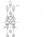
- Fig. 2 shows an example of the configuration of an antenna device using conventional technology.
- the antenna device 2 ′ is not disclosed in Patent Documents 1 and 2.
- antenna elements are arranged in a grid pattern on a plane.
- the antenna elements arranged in a lattice shape are divided into antenna elements 21 'in each column.
- the antenna elements 21 ′ in each row are two transmission lines 12 ′ extending in the opposite direction and connected to a waveguide / transmission line converter 1 ′ disposed in the center of each row (as a modification, one paragraph before Power is supplied as described above).
- the dielectric substrate 13 ' is a plane on which the antenna elements are arranged in a lattice pattern.
- the cross section of the wide wall surface of the waveguide 11 ′ is arranged in a direction perpendicular to the direction of each row.
- the cross section of the narrow wall surface of the waveguide 11 ' is arranged in a direction parallel to the direction of each row.
- the antenna elements 21 'in each column are fed at the center of each column, even if the excitation phases of the antenna elements constituting each column are shifted from each other at a frequency shifted from the center frequency of the antenna device 2', As a result of combining the antenna elements constituting the column, directivity with high gain can be formed in any one direction in a wide frequency range.
- the size p w ′ in the direction along the cross section of the wide wall surface of the waveguide 11 ′ among the sizes of the patterns arranged on the surface of the dielectric substrate 13 ′ (See FIG. 1). Therefore, 'in each column of the antenna elements 21 adjacent to each other' antenna device 2 distance d 'is inevitably wider than the length lambda 0/2 is equal to half the wavelength lambda 0 of the electromagnetic wave having radiated .
- the visible region in the array antenna must be wide, and in the directivity of the array antenna formed by each antenna element constituting each column, in particular, the phase information of each antenna element is adjusted to a wide angle. When scanning the beam, grating lobes in the array antenna are likely to occur.
- the present disclosure provides a waveguide / transmission line converter in a direction along a cross section of a wide wall surface of a waveguide among the sizes of patterns arranged on the surface of a dielectric substrate.
- the interval between the antenna elements adjacent to each other is narrowed, and in the directivity of the array antenna formed by each antenna element constituting each column, in particular, each antenna element It is an object of the present invention to make it difficult to generate a grating lobe when the phase information is adjusted and the beam is scanned to a wide angle.
- a current flowing through a narrow wall surface flows in a direction parallel to the cross section of the narrow wall surface. Applied that electromagnetic waves are not emitted when provided. That is, the metal member for extending the waveguide into the dielectric substrate and holding the short-circuit metal layer at the same potential as the waveguide is left along the cross section of the two wide wall surfaces of the waveguide, Except along the cross section of one of the two surfaces of the waveguide or the narrow wall surface of one surface, the electromagnetic wave is prevented from being inadvertently emitted.
- the present disclosure is a waveguide / transmission line converter that mutually converts power transmitted by a waveguide and power transmitted by a transmission line, A dielectric substrate disposed so as to close the opening; and the dielectric substrate disposed along the surface of the dielectric substrate and outside the waveguide, along a cross section of two wide wall surfaces of the waveguide. Or by a metal member penetrating the dielectric substrate along a cross section of one of the two wide wall surfaces and the two narrow wall surfaces of the waveguide. A short-circuited metal layer held at the same potential as the wave tube, disposed on the surface of the dielectric substrate and inside the waveguide, coupled to the transmission line, and having an effective wavelength in an environment around the dielectric substrate.
- the resonance length for raising an electromagnetic wave as a standing wave is defined as the direction of the electric field in the waveguide.
- a waveguide / transmission line converter characterized in that it comprises a matching element having a feeding direction of the transmission line.
- the size in the direction along the cross section of the wide wall surface of the waveguide can be reduced.
- the present disclosure is a waveguide / transmission line converter further including a dielectric layer formed on a surface of the transmission line and the short-circuit metal layer.
- the effective dielectric constant in the environment around the waveguide / transmission line converter can be increased, and the size of the pattern around the waveguide / transmission line converter can be reduced.
- the thickness of the dielectric layer is 0.2 times or less the effective wavelength of the electromagnetic wave in the environment around the waveguide / transmission line converter. / Transmission line converter.
- a plurality of the transmission lines extend in at least one of the two directions away from the waveguide / transmission line converter along the resonance length direction of the matching element. Is a waveguide / transmission line converter.
- an antenna can be arranged in a direction perpendicular to the feeding direction with only one waveguide / transmission line converter, and a high degree of freedom is imparted to the performance of the array antenna.
- the present disclosure is an antenna device in which antenna elements are arranged in a grid pattern on a plane, and the antenna elements arranged in a grid pattern are divided into antenna elements arranged in each column shape,
- the antenna elements arranged in the antenna are fed by the transmission line connected to the waveguide / transmission line converter arranged in the center of each row, and the antenna elements are arranged in a lattice pattern on the dielectric substrate.
- the cross section of the wide wall surface of the waveguide is arranged in a direction perpendicular to the direction of each row, and the cross section of the narrow wall surface of the waveguide is arranged in a direction parallel to the direction of each row. This is an antenna device.
- the distance between the antenna elements in each column adjacent to each other is narrowed, and in particular, the phase information of each antenna element is adjusted in the directivity of the array antenna formed by each antenna element constituting each column.
- the size along the cross section of the wide wall surface of the waveguide is reduced.
- the distance between the antenna elements in each column adjacent to each other is narrowed, and the phase information of each antenna element is adjusted particularly in the directivity of the array antenna formed by each antenna element constituting each column.
- FIG. 1 The configuration of the waveguide / transmission line converter of the first embodiment is shown in FIG.
- the uppermost stage shows a side sectional view of the waveguide / transmission line converter 1.
- the second stage shows an AA plane cross-sectional view of the waveguide / transmission line converter 1.
- the third stage shows a cross-sectional view taken along the line BB of the waveguide / transmission line converter 1.
- the bottom row shows the electric field distribution in the direction of the resonance length of the matching element 17 described later.
- the waveguide / transmission line converter 1 includes a dielectric substrate 13, a short-circuit metal layer 14, a metal member 15, a ground metal layer 16, and a matching element 17.
- the dielectric substrate 13 is disposed so as to close the opening of the waveguide 11.
- the surface of the dielectric substrate 13 is a surface perpendicular to the waveguide direction of the waveguide 11.
- the portion of the dielectric substrate 13 where the pattern is arranged is shown in white, and the portion of the dielectric substrate 13 where the pattern is not arranged is shown by diagonal lines.
- the short-circuit metal layer 14 is disposed on the surface of the dielectric substrate 13 and outside the waveguide 11, and the metal member 15 penetrating the dielectric substrate 13 along the cross section of the two wide wall surfaces of the waveguide 11 and the dielectric.
- the surface of the body substrate 13 and the ground metal layer 16 disposed on the outer frame of the waveguide 11 are held at the same potential as the waveguide 11. That is, the metal member 15 and the ground metal layer 16 for extending the waveguide 11 into the dielectric substrate 13 and holding the short-circuit metal layer 14 at the same potential as the waveguide 11 are formed on the two surfaces of the waveguide 11. In this case, the electromagnetic wave is not inadvertently radiated except for the cross section of the narrow wall surface of the two surfaces of the waveguide 11.
- the matching element 17 is disposed on the surface of the dielectric substrate 13 and inside the waveguide 11, is electromagnetically coupled to the transmission line 12 via the dielectric substrate 13, and has an effective wavelength in the environment around the dielectric substrate 13.
- a resonance length (approximately ⁇ g ′ / 2) for raising an electromagnetic wave of ⁇ g ′ as a standing wave is provided in the electric field direction in the waveguide 11 and the feeding direction of the transmission line 12.
- the matching element 17 and the transmission line 12 exist in different layers.
- tip shape of the transmission line 12 is a stub or slot with a notch. Therefore, the matching element 17 and the transmission line 12 can realize electromagnetic coupling.
- the metal member 15 is formed as a “through hole” that penetrates the dielectric substrate 13 along the cross section of the two wide wall surfaces of the waveguide 11.
- the metal member 15 may be a “conductor wall” that penetrates the dielectric substrate 13 along the cross section of the two wide wall surfaces of the waveguide 11.
- the metal member 15 penetrates the dielectric substrate 13 along the cross section of the two wide wall surfaces of the waveguide 11 and the narrow wall surface of one of the two surfaces. It may be formed by a “hole”.
- the metal member 15 includes a “conductor” penetrating the dielectric substrate 13 along a cross section of one of the two wide walls and one of the two walls of the waveguide 11. It may be a “wall”.
- only one transmission line 12 is arranged.
- two transmission lines 12 extending in opposite directions may be arranged.
- the two transmission lines 12 extending in the opposite directions may share one matching element 17.
- FIG. 4 shows the characteristics of the waveguide / transmission line converter according to the first embodiment.
- the first embodiment as in the prior art, low reflection characteristics and high transmission characteristics can be realized even at a frequency shifted from the center frequency of the waveguide / transmission line converter 1 by the bandwidth. is there.
- the size p W1 in the direction along the cross section of the wide wall surface of the waveguide 11 out of the sizes of the patterns arranged on the surface of the dielectric substrate 13 as compared with the prior art (see FIG. see 3.) the removal width of the metal member 15 and the grounding metallic layer 16 which has been removed along one or both sides of the narrow walls of the cross section of the two surfaces of the waveguide 11 2n W1 or n W1 (FIG. 3 Can be reduced by the amount of Specifically, the size p W1 in FIG. 3 is about 2/3 in the millimeter wave application in which the dimension of the metal member 15 is not negligible compared to the size p W ′ in FIG.
- the antenna elements are arranged in a grid pattern on a plane.
- the waveguide / transmission line converter 1 is arranged on a straight line in the horizontal direction of the drawing.
- the waveguide / transmission line converters 1 are arranged in a staggered manner in the left-right direction of the drawing.
- the antenna elements arranged in a lattice shape are divided into antenna elements 21 in each column.
- the antenna elements 21 in each row are two transmission lines 12 extending in opposite directions connected to the waveguide / transmission line converter 1 disposed in the center of each row (as described in the second paragraph before as a modification). )).
- the dielectric substrate 13 is a plane on which antenna elements are arranged in a lattice pattern.
- the cross section of the wide wall surface of the waveguide 11 is arranged in a direction perpendicular to the direction of each row.
- the section of the narrow wall surface of the waveguide 11 is arranged in a direction parallel to the direction of each row.
- the size p W1 in the direction along the cross section of the wide wall surface of the waveguide 11 among the sizes of the patterns arranged on the surface of the dielectric substrate 13 see FIG. 3). .
- width 2n W1 or n W1 see removed width 2n W1 or n W1 (FIG. 3 of the metal member 15 and the grounding metallic layer 16 which has been removed along the cross-section of the both surfaces or one surface of the narrow walls of the two surfaces of the waveguide 11.
- the size p W1 in FIG. 3 is about 2/3 in the millimeter wave application in which the dimension of the metal member 15 is not negligible compared to the size p W ′ in FIG.
- the antenna device 2 the distance d 1 of each row of antenna elements 21 adjacent to each other may be smaller than half the length equal lambda 0/2 of the wavelength lambda 0 of the electromagnetic wave having radiated, the array antenna In the directivity of the array antenna formed by each antenna element constituting each row, especially when adjusting the phase information of each antenna element and scanning the beam to a wide angle The grating lobe in the array antenna is less likely to occur.
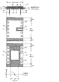
- the configuration of the waveguide / transmission line converter of the second embodiment is shown in FIG.
- the uppermost stage shows a side sectional view of the waveguide / transmission line converter 3.
- the second stage shows a cross-sectional plan view taken along the line CC of the waveguide / transmission line converter 3.
- the third stage shows a cross-sectional view taken along the line DD of the waveguide / transmission line converter 3.
- the bottom row shows the electric field distribution in the direction of the resonance length of the matching element 37 described later.
- the waveguide / transmission line converter 3 includes a dielectric substrate 33, a short-circuit metal layer 34, and the like so as to mutually convert the power transmitted by the waveguide 31 and the power transmitted by the transmission line 32.
- a metal member 35, a ground metal layer 36, a matching element 37, and a dielectric layer 30 are provided.
- the waveguide 31, transmission line 32, dielectric substrate 33, short-circuit metal layer 34, metal member 35, ground metal layer 36 and matching element 37 of the second embodiment in FIG. 7 are the same as those of the first embodiment in FIG.
- the wave tube 11, the transmission line 12, the dielectric substrate 13, the short-circuit metal layer 14, the metal member 15, the ground metal layer 16, and the matching element 17 are substantially the same.
- the matching element 37 is disposed on the surface of the dielectric substrate 33 and inside the waveguide 31, is electromagnetically coupled to the transmission line 32 via the dielectric substrate 33, and has an effective wavelength ⁇ in the environment around the matching element 37.
- the resonance length (approximately ⁇ g / 2) for standing up the electromagnetic wave of g (described later together with the dielectric layer 30) as a standing wave is provided in the direction of the electric field in the waveguide 31 and the feeding direction of the transmission line 32.
- the dielectric layer 30 is formed in close contact with or close to the surfaces of the transmission line 32 and the short-circuit metal layer 34. Therefore, in the second embodiment, the effective dielectric constant in the environment around the waveguide / transmission line converter 3 can be increased compared to the first embodiment, and the waveguide / transmission line converter 3 can be increased. of it is possible to shorten the electromagnetic effective wavelength lambda g of the environment around, it is possible to reduce the size p N2, p W2 direction along the narrow wall and wide walls of the cross section of the waveguide 31.
- the thickness of the dielectric layer 30 is preferably more than 0.2 times the electromagnetic radiation of an effective wavelength lambda g of the environment surrounding the waveguide / transmission line converter 3. Then, in order to cover the region where the electric field leaks from the dielectric substrate 33 between the transmission line 32 and the matching element 37, it is sufficient to form the dielectric layer 30 having a minimum thickness. Then, but only in the thickness (0.5mm or less extent) is thinner millimeter wave applications of the dielectric substrate 33, a dielectric layer 30 of minimal thickness (lambda g 0.2 times or less) However, the strength of the waveguide / transmission line converter 3 can be increased, and the size of the waveguide / transmission line converter 3 can be reduced. In the description of FIG. 7, the dielectric layer 30 is formed only on the surfaces of the transmission line 32 and the short-circuit metal layer 34. As a modification of FIG. 7, the dielectric layer 30 may be formed on the entire surface of the dielectric substrate 33.
- FIG. 1 shows a side sectional view of the waveguide / transmission line converter 4.
- the second stage shows a cross-sectional view taken along the line EE of the waveguide / transmission line converter 4.
- the third stage shows an FF plane cross-sectional view of the waveguide / transmission line converter 4 as viewed in the direction of the arrows.
- the bottom row shows the electric field distribution in the direction of the resonance length of the matching element 47 described later.
- the waveguide / transmission line converter 4 includes a dielectric substrate 43, a short-circuit metal layer 44, and the like, in order to convert between the power transmitted by the waveguide 41 and the power transmitted by the transmission line 42.
- a metal member 45, a ground metal layer 46, a matching element 47, and a dielectric layer 40 are provided.
- the waveguide 41, transmission line 42, dielectric substrate 43, short-circuit metal layer 44, metal member 45, ground metal layer 46, matching element 47, dielectric layer 40, size p N3 , p of the third embodiment in FIG. W3 and effective wavelength ⁇ g are the waveguide 31, transmission line 32, dielectric substrate 33, short-circuit metal layer 34, metal member 35, ground metal layer 36, matching element 37, dielectric of the second embodiment in FIG.
- the layers 30, the sizes p N2 and p W2 and the effective wavelength ⁇ g are substantially the same.
- two transmission lines 42 extend in both directions in two directions away from the waveguide / transmission line converter 4 along the resonance length direction of the matching element 47.
- a plurality of transmission lines 42 extend in one direction out of the two directions away from the waveguide / transmission line converter 4 along the resonance length direction of the matching element 47.
- one or a plurality of transmission lines 42 may extend in the other direction.
- the antenna arrangement can be made in the direction perpendicular to the feeding direction with only one waveguide / transmission line converter 4, and a high degree of freedom is given to the performance of the array antenna.
- the antenna elements are arranged in a grid pattern on a plane.
- the waveguide / transmission line converter 4 is arranged on a straight line in the horizontal direction of the drawing.
- the waveguide / transmission line converters 4 are arranged in a staggered manner in the left-right direction of the drawing.
- the antenna elements arranged in a lattice shape are divided into two rows of antenna elements 51. Each of the two rows of antenna elements 51 is connected to the waveguide / transmission line converter 4 arranged in the center of each of the two rows, and each of the two transmission lines 42 extends in the opposite direction (FIG. 8 as a third embodiment). The power is supplied as described above.
- the dielectric substrate 43 is a plane on which antenna elements are arranged in a lattice pattern.
- the cross section of the wide wall surface of the waveguide 41 is arranged in a direction perpendicular to the direction of each two rows.
- the cross section of the narrow wall surface of the waveguide 41 is arranged in a direction parallel to the direction of each two rows.
- the size p W3 in the direction along the cross section of the wide wall surface of the waveguide 41 among the sizes of the patterns arranged on the surface of the dielectric substrate 43 (see FIG. 8). Is the removal width 2nW3 or nW3 (see FIG. 8) of the metal member 45 and the ground metal layer 46 excluding the cross section of one of the two surfaces of the waveguide 41 or the narrow wall surface of one surface. )) Can be reduced.
- the size p W3 in FIG. 8 is about 2/3 in the millimeter wave application in which the dimension of the metal member 45 is not negligible compared to the size p W ′ in FIG.
- the distance d 3 of each row of antenna elements adjacent to each other may be narrower than a half length equal to lambda 0/2 of the wavelength lambda 0 of the electromagnetic wave has emitted.
- the waveguide / transmission line converter and the antenna device according to the present disclosure can form a high directivity with a high gain in any one direction in a wide frequency range with a combined result, hardly generate a grating lobe, and an antenna element on a plane
- the antenna device arranged in a lattice shape can be applied for the purpose of downsizing and cost reduction.
Abstract
The objectives of this disclosure are: to reduce the size, from among the sizes of a pattern disposed on an obverse surface of a dielectric substrate, in a direction along a wide-wall surface cross section of a waveguide tube, in a waveguide tube/transmission line converter; to reduce the separation between adjacent rows of antenna elements, in an antenna device; and, with regard to directionality of an array antenna formed by means of the antenna elements that form each row, to adjust in particular phase information of each antenna element in order to reduce the likelihood that grating lobes will occur when a beam is scanned over a wide angle. In this disclosure, inadvertent emission of electromagnetic waves is prevented by arranging that a waveguide tube 11 extends on the inside of a dielectric substrate 13, and that metal members 15 for holding a short-circuiting metal layer 14 at the same potential as the waveguide tube 11 remain along the two wide-wall surface cross sections of the waveguide tube 11, and are removed along the two short-wall surface cross sections of the waveguide tube 11.
Description
本開示は、(1)導波管により伝送される電力と、伝送線路により伝送される電力と、を相互に変換する導波管/伝送線路変換器、及び、(2)アンテナ素子が平面上に格子状に配置され導波管/伝送線路変換器により給電されるアンテナ装置に関する。
The present disclosure includes: (1) a waveguide / transmission line converter that mutually converts power transmitted by a waveguide and power transmitted by a transmission line; and (2) an antenna element on a plane. The present invention relates to an antenna device which is arranged in a grid pattern and is fed by a waveguide / transmission line converter.
導波管/伝送線路変換器は、アンテナ装置への給電等に適用されており、特許文献1、2等に開示されている。まず、特許文献1では、導波管内の電界強度の高い位置において、伝送線路を挿入している。しかし、特許文献1では、導波管内の電磁波が有する波長のほぼ1/4に等しい距離分だけ、導波管に沿って伝送線路から離れた位置において、導波管短絡面を必要とする。よって、特許文献1では、導波管/伝送線路変換器を小型化することができず、短絡面を形成する構造体が、アンテナ装置を形成する面より前面に存在するため、アンテナ装置の指向性の劣化原因となる。
The waveguide / transmission line converter is applied to power feeding to the antenna device and is disclosed in Patent Documents 1 and 2 and the like. First, in Patent Document 1, a transmission line is inserted at a position where the electric field strength is high in the waveguide. However, in Patent Document 1, a waveguide short-circuit surface is required at a position that is separated from the transmission line along the waveguide by a distance equal to approximately ¼ of the wavelength of the electromagnetic wave in the waveguide. Therefore, in Patent Document 1, the waveguide / transmission line converter cannot be reduced in size, and the structure that forms the short-circuited surface exists in front of the surface that forms the antenna device. Cause deterioration of sex.
次に、特許文献2では、整合素子に伝送線路を結合し、伝送線路から導波管へ電波を伝搬する技術を利用している。以下の説明から明らかなように、特許文献2では、特許文献1と比べて、導波管/伝送線路変換器を小型化することができ、アンテナ装置の指向性を劣化させる原因となる短絡面を形成する構造体を無くすことができる。
Next, in Patent Document 2, a technique of coupling a transmission line to a matching element and propagating radio waves from the transmission line to a waveguide is used. As will be apparent from the following description, in Patent Document 2, the waveguide / transmission line converter can be reduced in size compared to Patent Document 1, and the short-circuit surface that causes the directivity of the antenna device to deteriorate. The structure which forms can be eliminated.
従来技術の導波管/伝送線路変換器の構成を図1に示す。最上段は、導波管/伝送線路変換器1’の側面断面図を示す。第2段は、導波管/伝送線路変換器1’の矢視A’-A’平面断面図を示す。第3段は、導波管/伝送線路変換器1’の矢視B’-B’平面断面図を示す。最下段は、後述する整合素子17’の共振長の方向の電界分布を示す。
Fig. 1 shows the configuration of a conventional waveguide / transmission line converter. The top row shows a side sectional view of the waveguide / transmission line converter 1 '. The second stage shows a cross-sectional view of the waveguide / transmission line converter 1 'taken along the arrow A'-A'. The third stage shows a cross-sectional plan view of the waveguide / transmission line converter 1 'taken along the arrow B'-B'. The bottom row shows the electric field distribution in the direction of the resonance length of the matching element 17 'described later.
導波管/伝送線路変換器1’は、誘電体基板13’、短絡金属層14’、金属部材15’、接地金属層16’及び整合素子17’を備える。
The waveguide / transmission line converter 1 ′ includes a dielectric substrate 13 ′, a short-circuit metal layer 14 ′, a metal member 15 ′, a ground metal layer 16 ′, and a matching element 17 ′.
誘電体基板13’は、導波管11’の開口部を塞ぐように配置される。誘電体基板13’の面は、導波管11’の導波方向に垂直な面である。図1の第2、3段において、誘電体基板13’のうちパターンが配置される部分は、白地で示され、誘電体基板13’のうちパターンが配置されない部分は、斜線で示される。
The dielectric substrate 13 ′ is disposed so as to close the opening of the waveguide 11 ′. The surface of the dielectric substrate 13 ′ is a surface perpendicular to the waveguide direction of the waveguide 11 ′. In the second and third stages of FIG. 1, the portion of the dielectric substrate 13 ′ where the pattern is arranged is shown in white, and the portion of the dielectric substrate 13 ′ where the pattern is not arranged is shown in diagonal lines.
短絡金属層14’は、誘電体基板13’の表面かつ導波管11’の外部に配置され、誘電体基板13’を貫通する金属部材15’及び誘電体基板13’の表面かつ導波管11’の外枠に配置される接地金属層16’により、導波管11’と同電位に保持される。
The short-circuit metal layer 14 'is disposed on the surface of the dielectric substrate 13' and outside the waveguide 11 ', and the metal member 15' penetrating the dielectric substrate 13 'and the surface of the dielectric substrate 13' and the waveguide. The ground metal layer 16 'disposed on the outer frame of 11' is held at the same potential as the waveguide 11 '.
整合素子17’は、誘電体基板13’の表面かつ導波管11’の内部に配置され、誘電体基板13’を介して伝送線路12’と電磁的に結合され、誘電体基板13’の周囲の環境における実効波長λg’の電磁波を定在波として立てるための共振長(ほぼλg’/2)を、導波管11’内の電界方向及び伝送線路12’の給電方向に有する。
The matching element 17 ′ is disposed on the surface of the dielectric substrate 13 ′ and inside the waveguide 11 ′, and is electromagnetically coupled to the transmission line 12 ′ via the dielectric substrate 13 ′. A resonance length (approximately λ g ′ / 2) for standing an electromagnetic wave having an effective wavelength λ g ′ in the surrounding environment as a standing wave is provided in the electric field direction in the waveguide 11 ′ and the feeding direction of the transmission line 12 ′. .
図1の説明では、伝送線路12’は、ただ1本のみを配置されている。変形例としては、伝送線路12’は、逆方向に延びる2本を配置されてもよい。ただし、整合素子17’は、2枚も配置する必要はなく、ただ1枚のみを配置すれば足りる。そして、2本の逆方向に延びる伝送線路12’は、1枚の整合素子17’を共有すればよい。
In the description of FIG. 1, only one transmission line 12 'is arranged. As a modification, two transmission lines 12 ′ extending in opposite directions may be arranged. However, it is not necessary to arrange two matching elements 17 ', and only one matching element 17' is sufficient. The two transmission lines 12 ′ extending in opposite directions may share one matching element 17 ′.
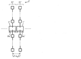
従来技術を利用したアンテナ装置の構成例を図2に示す。アンテナ装置2’は、特許文献1、2に開示されていない。アンテナ装置2’では、アンテナ素子が平面上に格子状に配置される。格子状に配置されるアンテナ素子は、各列のアンテナ素子21’に分割される。各列のアンテナ素子21’は、各列の中央に配置される導波管/伝送線路変換器1’ に接続される2本の逆方向に延びる伝送線路12’(変形例として1段落前に説明したものである。)により給電される。誘電体基板13’は、アンテナ素子が格子状に配置される平面である。導波管11’の広壁面の断面は、各列の方向に垂直な方向に配置される。導波管11’の狭壁面の断面は、各列の方向に平行な方向に配置される。
Fig. 2 shows an example of the configuration of an antenna device using conventional technology. The antenna device 2 ′ is not disclosed in Patent Documents 1 and 2. In the antenna device 2 ′, antenna elements are arranged in a grid pattern on a plane. The antenna elements arranged in a lattice shape are divided into antenna elements 21 'in each column. The antenna elements 21 ′ in each row are two transmission lines 12 ′ extending in the opposite direction and connected to a waveguide / transmission line converter 1 ′ disposed in the center of each row (as a modification, one paragraph before Power is supplied as described above). The dielectric substrate 13 'is a plane on which the antenna elements are arranged in a lattice pattern. The cross section of the wide wall surface of the waveguide 11 ′ is arranged in a direction perpendicular to the direction of each row. The cross section of the narrow wall surface of the waveguide 11 'is arranged in a direction parallel to the direction of each row.
各列のアンテナ素子21’が各列の中央で給電されることにより、アンテナ装置2’の中心周波数からずれた周波数において、各列を構成する各アンテナ素子の励振位相が互いにずれても、各列を構成する各アンテナ素子の合成結果は、広い周波数範囲で任意の一方向に利得の高い指向性を形成できる。
Since the antenna elements 21 'in each column are fed at the center of each column, even if the excitation phases of the antenna elements constituting each column are shifted from each other at a frequency shifted from the center frequency of the antenna device 2', As a result of combining the antenna elements constituting the column, directivity with high gain can be formed in any one direction in a wide frequency range.
しかし、導波管/伝送線路変換器1’において、誘電体基板13’の表面に配置されるパターンのサイズのうち、導波管11’の広壁面の断面に沿う方向のサイズpw’(図1を参照。)は、大きくならざるを得ない。よって、アンテナ装置2’において、互いに隣り合う各列のアンテナ素子21’の間隔d’は、放射される電磁波が有する波長λ0の半分に等しい長さλ0/2より広くならざるを得ない。これにより、アレーアンテナにおける可視領域は、広くならざるを得ず、各列を構成する各アンテナ素子により形成されるアレーアンテナの指向性において、特に、各アンテナ素子の位相情報を調整し、広角までビームを走査する際に、アレーアンテナにおけるグレーティングローブは、発生しやすくなる。
However, in the waveguide / transmission line converter 1 ′, the size p w ′ in the direction along the cross section of the wide wall surface of the waveguide 11 ′ among the sizes of the patterns arranged on the surface of the dielectric substrate 13 ′ ( (See FIG. 1). Therefore, 'in each column of the antenna elements 21 adjacent to each other' antenna device 2 distance d 'is inevitably wider than the length lambda 0/2 is equal to half the wavelength lambda 0 of the electromagnetic wave having radiated . As a result, the visible region in the array antenna must be wide, and in the directivity of the array antenna formed by each antenna element constituting each column, in particular, the phase information of each antenna element is adjusted to a wide angle. When scanning the beam, grating lobes in the array antenna are likely to occur.
そこで、前記課題を解決するために、本開示は、導波管/伝送線路変換器において、誘電体基板の表面に配置されるパターンのサイズのうち、導波管の広壁面の断面に沿う方向のサイズを小さくして、アンテナ装置において、互いに隣り合う各列のアンテナ素子の間隔を狭くして、各列を構成する各アンテナ素子により形成されるアレーアンテナの指向性において、特に、各アンテナ素子の位相情報を調整し、広角までビームを走査する際に、グレーティングローブを発生しにくくすることを目的とする。
Therefore, in order to solve the above-described problem, the present disclosure provides a waveguide / transmission line converter in a direction along a cross section of a wide wall surface of a waveguide among the sizes of patterns arranged on the surface of a dielectric substrate. In the antenna device, in the antenna device, the interval between the antenna elements adjacent to each other is narrowed, and in the directivity of the array antenna formed by each antenna element constituting each column, in particular, each antenna element It is an object of the present invention to make it difficult to generate a grating lobe when the phase information is adjusted and the beam is scanned to a wide angle.
上記目的を達成するために、導波管スロットアンテナにおいて、狭壁面を流れる電流が、狭壁面の断面に平行な方向に流れるところ、狭壁面に設けるスロットが、狭壁面の断面に平行な方向に設けられると、電磁波が放射されないことを応用した。すなわち、導波管を誘電体基板内に延長するとともに短絡金属層を導波管と同電位に保持するための金属部材を、導波管の2面の広壁面の断面に沿っては残し、導波管の2面のうちの両面又は片面の狭壁面の断面に沿っては除き、不用意に電磁波が放射されないようにする。
In order to achieve the above object, in a waveguide slot antenna, a current flowing through a narrow wall surface flows in a direction parallel to the cross section of the narrow wall surface. Applied that electromagnetic waves are not emitted when provided. That is, the metal member for extending the waveguide into the dielectric substrate and holding the short-circuit metal layer at the same potential as the waveguide is left along the cross section of the two wide wall surfaces of the waveguide, Except along the cross section of one of the two surfaces of the waveguide or the narrow wall surface of one surface, the electromagnetic wave is prevented from being inadvertently emitted.
具体的には、本開示は、導波管により伝送される電力と、伝送線路により伝送される電力と、を相互に変換する導波管/伝送線路変換器であって、前記導波管の開口部を塞ぐように配置される誘電体基板と、前記誘電体基板の表面かつ前記導波管の外部に配置され、前記導波管の2面の広壁面の断面に沿って前記誘電体基板を貫通する金属部材により、又は、前記導波管の2面の広壁面及び2面のうちのいずれか1面の狭壁面の断面に沿って前記誘電体基板を貫通する金属部材により、前記導波管と同電位に保持される短絡金属層と、前記誘電体基板の表面かつ前記導波管の内部に配置され、前記伝送線路と結合され、前記誘電体基板の周囲の環境における実効波長の電磁波を定在波として立てるための共振長を前記導波管内の電界方向及び前記伝送線路の給電方向に有する整合素子と、を備えることを特徴とする導波管/伝送線路変換器である。
Specifically, the present disclosure is a waveguide / transmission line converter that mutually converts power transmitted by a waveguide and power transmitted by a transmission line, A dielectric substrate disposed so as to close the opening; and the dielectric substrate disposed along the surface of the dielectric substrate and outside the waveguide, along a cross section of two wide wall surfaces of the waveguide. Or by a metal member penetrating the dielectric substrate along a cross section of one of the two wide wall surfaces and the two narrow wall surfaces of the waveguide. A short-circuited metal layer held at the same potential as the wave tube, disposed on the surface of the dielectric substrate and inside the waveguide, coupled to the transmission line, and having an effective wavelength in an environment around the dielectric substrate. The resonance length for raising an electromagnetic wave as a standing wave is defined as the direction of the electric field in the waveguide. A waveguide / transmission line converter, characterized in that it comprises a matching element having a feeding direction of the transmission line.
この構成によれば、誘電体基板の表面に配置されるパターンのサイズのうち、導波管の広壁面の断面に沿う方向のサイズを小さくすることができる。
According to this configuration, among the sizes of the patterns arranged on the surface of the dielectric substrate, the size in the direction along the cross section of the wide wall surface of the waveguide can be reduced.
また、本開示は、前記伝送線路及び前記短絡金属層の表面に形成される誘電体層、をさらに備えることを特徴とする導波管/伝送線路変換器である。
Also, the present disclosure is a waveguide / transmission line converter further including a dielectric layer formed on a surface of the transmission line and the short-circuit metal layer.
この構成によれば、導波管/伝送線路変換器の周囲の環境での実効誘電率を高くして、導波管/伝送線路変換器の周囲のパターンのサイズを小さくすることができる。
According to this configuration, the effective dielectric constant in the environment around the waveguide / transmission line converter can be increased, and the size of the pattern around the waveguide / transmission line converter can be reduced.
また、本開示は、前記誘電体層の厚さは、前記導波管/伝送線路変換器の周囲の環境での電磁波の実効波長の0.2倍以下であることを特徴とする導波管/伝送線路変換器である。
In the present disclosure, the thickness of the dielectric layer is 0.2 times or less the effective wavelength of the electromagnetic wave in the environment around the waveguide / transmission line converter. / Transmission line converter.
この構成によれば、伝送線路及び整合素子の間の誘電体基板から電界が漏れ出す領域をカバーするために、最小限の厚さの誘電体層を形成すれば足りるようになる。
According to this configuration, it is sufficient to form a dielectric layer having a minimum thickness in order to cover a region where the electric field leaks from the dielectric substrate between the transmission line and the matching element.
また、本開示は、前記整合素子の共振長の方向に沿って前記導波管/伝送線路変換器から離れる2方向のうち少なくとも1方向に向かって、複数本の前記伝送線路が延びていることを特徴とする導波管/伝送線路変換器である。
Further, in the present disclosure, a plurality of the transmission lines extend in at least one of the two directions away from the waveguide / transmission line converter along the resonance length direction of the matching element. Is a waveguide / transmission line converter.
この構成によれば、1台の導波管/伝送線路変換器のみで、給電方向と垂直方向にアンテナ配列が可能となり、アレーアンテナの性能に高い自由度が付与される。
According to this configuration, an antenna can be arranged in a direction perpendicular to the feeding direction with only one waveguide / transmission line converter, and a high degree of freedom is imparted to the performance of the array antenna.
また、本開示は、アンテナ素子が平面上に格子状に配置されるアンテナ装置であって、格子状に配置されるアンテナ素子は、各列状に配置されるアンテナ素子に分割され、各列状に配置されるアンテナ素子は、各列の中央に配置される導波管/伝送線路変換器に接続される前記伝送線路により給電され、前記誘電体基板は、アンテナ素子が格子状に配置される平面であり、前記導波管の広壁面の断面は、各列の方向に垂直な方向に配置され、前記導波管の狭壁面の断面は、各列の方向に平行な方向に配置されることを特徴とするアンテナ装置である。
In addition, the present disclosure is an antenna device in which antenna elements are arranged in a grid pattern on a plane, and the antenna elements arranged in a grid pattern are divided into antenna elements arranged in each column shape, The antenna elements arranged in the antenna are fed by the transmission line connected to the waveguide / transmission line converter arranged in the center of each row, and the antenna elements are arranged in a lattice pattern on the dielectric substrate. The cross section of the wide wall surface of the waveguide is arranged in a direction perpendicular to the direction of each row, and the cross section of the narrow wall surface of the waveguide is arranged in a direction parallel to the direction of each row. This is an antenna device.
この構成によれば、互いに隣り合う各列のアンテナ素子の間隔を狭くして、各列を構成する各アンテナ素子により形成されるアレーアンテナの指向性において、特に、各アンテナ素子の位相情報を調整し、広角までビームを走査する際に、グレーティングローブを発生しにくくすることができる。
According to this configuration, the distance between the antenna elements in each column adjacent to each other is narrowed, and in particular, the phase information of each antenna element is adjusted in the directivity of the array antenna formed by each antenna element constituting each column. However, it is possible to make it difficult to generate a grating lobe when the beam is scanned to a wide angle.
このように、本開示により、導波管/伝送線路変換器において、誘電体基板の表面に配置されるパターンのサイズのうち、導波管の広壁面の断面に沿う方向のサイズを小さくして、アンテナ装置において、互いに隣り合う各列のアンテナ素子の間隔を狭くして、各列を構成する各アンテナ素子により形成されるアレーアンテナの指向性において、特に、各アンテナ素子の位相情報を調整し、広角までビームを走査する際に、グレーティングローブを発生しにくくすることができる。
Thus, according to the present disclosure, in the waveguide / transmission line converter, among the sizes of the patterns arranged on the surface of the dielectric substrate, the size along the cross section of the wide wall surface of the waveguide is reduced. In the antenna apparatus, the distance between the antenna elements in each column adjacent to each other is narrowed, and the phase information of each antenna element is adjusted particularly in the directivity of the array antenna formed by each antenna element constituting each column. When scanning the beam to a wide angle, it is possible to make it difficult to generate grating lobes.
添付の図面を参照して本開示の実施形態を説明する。以下に説明する実施形態は本開示の実施の例であり、本開示は以下の実施形態に制限されるものではない。これらの実施の例は例示に過ぎず、本開示は当業者の知識に基づいて種々の変更、改良を施した形態で
実施することができる。なお、本明細書及び図面において符号が同じ構成要素は、相互に同一のものを示すものとする。 Embodiments of the present disclosure will be described with reference to the accompanying drawings. The embodiments described below are examples of the present disclosure, and the present disclosure is not limited to the following embodiments. These embodiments are merely examples, and the present disclosure can be implemented in various modifications and improvements based on the knowledge of those skilled in the art. In the present specification and drawings, the same reference numerals denote the same components.
実施することができる。なお、本明細書及び図面において符号が同じ構成要素は、相互に同一のものを示すものとする。 Embodiments of the present disclosure will be described with reference to the accompanying drawings. The embodiments described below are examples of the present disclosure, and the present disclosure is not limited to the following embodiments. These embodiments are merely examples, and the present disclosure can be implemented in various modifications and improvements based on the knowledge of those skilled in the art. In the present specification and drawings, the same reference numerals denote the same components.
(第1実施形態)
第1実施形態の導波管/伝送線路変換器の構成を図3に示す。最上段は、導波管/伝送線路変換器1の側面断面図を示す。第2段は、導波管/伝送線路変換器1の矢視A-A平面断面図を示す。第3段は、導波管/伝送線路変換器1の矢視B-B平面断面図を示す。最下段は、後述する整合素子17の共振長の方向の電界分布を示す。 (First embodiment)
The configuration of the waveguide / transmission line converter of the first embodiment is shown in FIG. The uppermost stage shows a side sectional view of the waveguide /transmission line converter 1. The second stage shows an AA plane cross-sectional view of the waveguide / transmission line converter 1. The third stage shows a cross-sectional view taken along the line BB of the waveguide / transmission line converter 1. The bottom row shows the electric field distribution in the direction of the resonance length of the matching element 17 described later.
第1実施形態の導波管/伝送線路変換器の構成を図3に示す。最上段は、導波管/伝送線路変換器1の側面断面図を示す。第2段は、導波管/伝送線路変換器1の矢視A-A平面断面図を示す。第3段は、導波管/伝送線路変換器1の矢視B-B平面断面図を示す。最下段は、後述する整合素子17の共振長の方向の電界分布を示す。 (First embodiment)
The configuration of the waveguide / transmission line converter of the first embodiment is shown in FIG. The uppermost stage shows a side sectional view of the waveguide /
導波管/伝送線路変換器1は、誘電体基板13、短絡金属層14、金属部材15、接地金属層16及び整合素子17を備える。
The waveguide / transmission line converter 1 includes a dielectric substrate 13, a short-circuit metal layer 14, a metal member 15, a ground metal layer 16, and a matching element 17.
誘電体基板13は、導波管11の開口部を塞ぐように配置される。誘電体基板13の面は、導波管11の導波方向に垂直な面である。図3の第2、3段において、誘電体基板13のうちパターンが配置される部分は、白地で示され、誘電体基板13のうちパターンが配置されない部分は、斜線で示される。
The dielectric substrate 13 is disposed so as to close the opening of the waveguide 11. The surface of the dielectric substrate 13 is a surface perpendicular to the waveguide direction of the waveguide 11. In the second and third stages of FIG. 3, the portion of the dielectric substrate 13 where the pattern is arranged is shown in white, and the portion of the dielectric substrate 13 where the pattern is not arranged is shown by diagonal lines.
短絡金属層14は、誘電体基板13の表面かつ導波管11の外部に配置され、導波管11の2面の広壁面の断面に沿って誘電体基板13を貫通する金属部材15及び誘電体基板13の表面かつ導波管11の外枠に配置される接地金属層16により、導波管11と同電位に保持される。すなわち、導波管11を誘電体基板13内に延長するとともに短絡金属層14を導波管11と同電位に保持するための金属部材15及び接地金属層16を、導波管11の2面の広壁面の断面に沿っては残し、導波管11の2面の狭壁面の断面に沿っては除き、不用意に電磁波が放射されないようにする。
The short-circuit metal layer 14 is disposed on the surface of the dielectric substrate 13 and outside the waveguide 11, and the metal member 15 penetrating the dielectric substrate 13 along the cross section of the two wide wall surfaces of the waveguide 11 and the dielectric. The surface of the body substrate 13 and the ground metal layer 16 disposed on the outer frame of the waveguide 11 are held at the same potential as the waveguide 11. That is, the metal member 15 and the ground metal layer 16 for extending the waveguide 11 into the dielectric substrate 13 and holding the short-circuit metal layer 14 at the same potential as the waveguide 11 are formed on the two surfaces of the waveguide 11. In this case, the electromagnetic wave is not inadvertently radiated except for the cross section of the narrow wall surface of the two surfaces of the waveguide 11.
整合素子17は、誘電体基板13の表面かつ導波管11の内部に配置され、誘電体基板13を介して伝送線路12と電磁的に結合され、誘電体基板13の周囲の環境における実効波長λg’の電磁波を定在波として立てるための共振長(ほぼλg’/2)を、導波管11内の電界方向及び伝送線路12の給電方向に有する。
The matching element 17 is disposed on the surface of the dielectric substrate 13 and inside the waveguide 11, is electromagnetically coupled to the transmission line 12 via the dielectric substrate 13, and has an effective wavelength in the environment around the dielectric substrate 13. A resonance length (approximately λ g ′ / 2) for raising an electromagnetic wave of λ g ′ as a standing wave is provided in the electric field direction in the waveguide 11 and the feeding direction of the transmission line 12.
ここで、整合素子17及び伝送線路12は、別層に存在する。そして、伝送線路12の先端形状は、切り欠き付きのスタブ又はスロットである。よって、整合素子17及び伝送線路12は、電磁的な結合を実現することができる。
Here, the matching element 17 and the transmission line 12 exist in different layers. And the front-end | tip shape of the transmission line 12 is a stub or slot with a notch. Therefore, the matching element 17 and the transmission line 12 can realize electromagnetic coupling.
図3の説明では、金属部材15は、導波管11の2面の広壁面の断面に沿って誘電体基板13を貫通する「スルーホール」で形成されている。第1の変形例として、金属部材15は、導波管11の2面の広壁面の断面に沿って誘電体基板13を貫通する「導体壁」であってもよい。第2の変形例として、金属部材15は、導波管11の2面の広壁面及び2面のうちのいずれかの1面の狭壁面の断面に沿って誘電体基板13を貫通する「スルーホール」で形成されていてもよい。第3の変形例として、金属部材15は、導波管11の2面の広壁面及び2面のうちのいずれかの1面の狭壁面の断面に沿って誘電体基板13を貫通する「導体壁」であってもよい。
In the description of FIG. 3, the metal member 15 is formed as a “through hole” that penetrates the dielectric substrate 13 along the cross section of the two wide wall surfaces of the waveguide 11. As a first modification, the metal member 15 may be a “conductor wall” that penetrates the dielectric substrate 13 along the cross section of the two wide wall surfaces of the waveguide 11. As a second modification, the metal member 15 penetrates the dielectric substrate 13 along the cross section of the two wide wall surfaces of the waveguide 11 and the narrow wall surface of one of the two surfaces. It may be formed by a “hole”. As a third modification, the metal member 15 includes a “conductor” penetrating the dielectric substrate 13 along a cross section of one of the two wide walls and one of the two walls of the waveguide 11. It may be a “wall”.
図3の説明では、伝送線路12は、ただ1本のみを配置されている。変形例としては、伝送線路12は、逆方向に延びる2本を配置されてもよい。ただし、整合素子17は、2枚も配置する必要はなく、ただ1枚のみを配置すれば足りる。そして、2本の逆方向に延びる伝送線路12は、1枚の整合素子17を共有すればよい。
In the description of FIG. 3, only one transmission line 12 is arranged. As a modification, two transmission lines 12 extending in opposite directions may be arranged. However, it is not necessary to arrange two matching elements 17 and it is sufficient to arrange only one matching element 17. The two transmission lines 12 extending in the opposite directions may share one matching element 17.
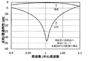
第1実施形態の導波管/伝送線路変換器の特性を図4に示す。このように、第1実施形態では、従来技術と同様に、導波管/伝送線路変換器1の中心周波数から帯域幅分だけずれた周波数においても、低い反射特性及び高い透過特性を実現可能である。
FIG. 4 shows the characteristics of the waveguide / transmission line converter according to the first embodiment. As described above, in the first embodiment, as in the prior art, low reflection characteristics and high transmission characteristics can be realized even at a frequency shifted from the center frequency of the waveguide / transmission line converter 1 by the bandwidth. is there.
これに加え、第1実施形態では、従来技術と比べて、誘電体基板13の表面に配置されるパターンのサイズのうち、導波管11の広壁面の断面に沿う方向のサイズpW1(図3を参照。)は、導波管11の2面のうちの両面又は片面の狭壁面の断面に沿っては除いた金属部材15及び接地金属層16の除去幅2nW1又はnW1(図3を参照。)の分だけ、小さくすることができる。具体的には、図3のサイズpW1は、図1のサイズpW’と比べて、金属部材15の寸法が無視できないミリ波応用において、約2/3となる。
In addition, in the first embodiment, the size p W1 in the direction along the cross section of the wide wall surface of the waveguide 11 out of the sizes of the patterns arranged on the surface of the dielectric substrate 13 as compared with the prior art (see FIG. see 3.) the removal width of the metal member 15 and the grounding metallic layer 16 which has been removed along one or both sides of the narrow walls of the cross section of the two surfaces of the waveguide 11 2n W1 or n W1 (FIG. 3 Can be reduced by the amount of Specifically, the size p W1 in FIG. 3 is about 2/3 in the millimeter wave application in which the dimension of the metal member 15 is not negligible compared to the size p W ′ in FIG.
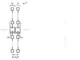
第1実施形態のアンテナ装置の構成を図5、6に示す。アンテナ装置2では、アンテナ素子が平面上に格子状に配置される。図5では、導波管/伝送線路変換器1は、図面左右方向に直線上に配置される。図6では、導波管/伝送線路変換器1は、図面左右方向に千鳥状に配置される。格子状に配置されるアンテナ素子は、各列のアンテナ素子21に分割される。各列のアンテナ素子21は、各列の中央に配置される導波管/伝送線路変換器1に接続される2本の逆方向に延びる伝送線路12(変形例として2段落前に説明したものである。)により給電される。誘電体基板13は、アンテナ素子が格子状に配置される平面である。導波管11の広壁面の断面は、各列の方向に垂直な方向に配置される。導波管11の狭壁面の断面は、各列の方向に平行な方向に配置される。
The configuration of the antenna device of the first embodiment is shown in FIGS. In the antenna device 2, the antenna elements are arranged in a grid pattern on a plane. In FIG. 5, the waveguide / transmission line converter 1 is arranged on a straight line in the horizontal direction of the drawing. In FIG. 6, the waveguide / transmission line converters 1 are arranged in a staggered manner in the left-right direction of the drawing. The antenna elements arranged in a lattice shape are divided into antenna elements 21 in each column. The antenna elements 21 in each row are two transmission lines 12 extending in opposite directions connected to the waveguide / transmission line converter 1 disposed in the center of each row (as described in the second paragraph before as a modification). )). The dielectric substrate 13 is a plane on which antenna elements are arranged in a lattice pattern. The cross section of the wide wall surface of the waveguide 11 is arranged in a direction perpendicular to the direction of each row. The section of the narrow wall surface of the waveguide 11 is arranged in a direction parallel to the direction of each row.
各列のアンテナ素子21が各列の中央で給電されることにより、アンテナ装置2の中心周波数からずれた周波数において、各列を構成する各アンテナ素子の励振位相が互いにずれても、各列を構成する各アンテナ素子の合成結果は、広い周波数範囲で任意の一方向に利得の高い指向性を形成できる。
By feeding the antenna elements 21 of each column at the center of each column, even if the excitation phases of the antenna elements constituting each column are shifted from each other at a frequency shifted from the center frequency of the antenna device 2, As a result of synthesizing the respective antenna elements, a directivity having a high gain can be formed in one arbitrary direction in a wide frequency range.
そして、導波管/伝送線路変換器1において、誘電体基板13の表面に配置されるパターンのサイズのうち、導波管11の広壁面の断面に沿う方向のサイズpW1(図3を参照。)は、導波管11の2面のうちの両面又は片面の狭壁面の断面に沿っては除いた金属部材15及び接地金属層16の除去幅2nW1又はnW1(図3を参照。)の分だけ、小さくすることができる。具体的には、図3のサイズpW1は、図1のサイズpW’と比べて、金属部材15の寸法が無視できないミリ波応用において、約2/3となる。
In the waveguide / transmission line converter 1, the size p W1 in the direction along the cross section of the wide wall surface of the waveguide 11 among the sizes of the patterns arranged on the surface of the dielectric substrate 13 (see FIG. 3). .), see removed width 2n W1 or n W1 (FIG. 3 of the metal member 15 and the grounding metallic layer 16 which has been removed along the cross-section of the both surfaces or one surface of the narrow walls of the two surfaces of the waveguide 11. ) Can be made smaller. Specifically, the size p W1 in FIG. 3 is about 2/3 in the millimeter wave application in which the dimension of the metal member 15 is not negligible compared to the size p W ′ in FIG.
よって、アンテナ装置2において、互いに隣り合う各列のアンテナ素子21の間隔d1は、放射される電磁波が有する波長λ0の半分に等しい長さλ0/2より狭くすることができ、アレーアンテナにおける可視領域は、狭くすることができ、各列を構成する各アンテナ素子により形成されるアレーアンテナの指向性において、特に、各アンテナ素子の位相情報を調整し、広角までビームを走査する際に、アレーアンテナにおけるグレーティングローブは、発生しにくくなる。
Therefore, the antenna device 2, the distance d 1 of each row of antenna elements 21 adjacent to each other may be smaller than half the length equal lambda 0/2 of the wavelength lambda 0 of the electromagnetic wave having radiated, the array antenna In the directivity of the array antenna formed by each antenna element constituting each row, especially when adjusting the phase information of each antenna element and scanning the beam to a wide angle The grating lobe in the array antenna is less likely to occur.
(第2実施形態)
第2実施形態の導波管/伝送線路変換器の構成を図7に示す。最上段は、導波管/伝送線路変換器3の側面断面図を示す。第2段は、導波管/伝送線路変換器3の矢視C-C平面断面図を示す。第3段は、導波管/伝送線路変換器3の矢視D-D平面断面図を示す。最下段は、後述する整合素子37の共振長の方向の電界分布を示す。 (Second embodiment)
The configuration of the waveguide / transmission line converter of the second embodiment is shown in FIG. The uppermost stage shows a side sectional view of the waveguide / transmission line converter 3. The second stage shows a cross-sectional plan view taken along the line CC of the waveguide / transmission line converter 3. The third stage shows a cross-sectional view taken along the line DD of the waveguide / transmission line converter 3. The bottom row shows the electric field distribution in the direction of the resonance length of the matchingelement 37 described later.
第2実施形態の導波管/伝送線路変換器の構成を図7に示す。最上段は、導波管/伝送線路変換器3の側面断面図を示す。第2段は、導波管/伝送線路変換器3の矢視C-C平面断面図を示す。第3段は、導波管/伝送線路変換器3の矢視D-D平面断面図を示す。最下段は、後述する整合素子37の共振長の方向の電界分布を示す。 (Second embodiment)
The configuration of the waveguide / transmission line converter of the second embodiment is shown in FIG. The uppermost stage shows a side sectional view of the waveguide / transmission line converter 3. The second stage shows a cross-sectional plan view taken along the line CC of the waveguide / transmission line converter 3. The third stage shows a cross-sectional view taken along the line DD of the waveguide / transmission line converter 3. The bottom row shows the electric field distribution in the direction of the resonance length of the matching
導波管/伝送線路変換器3は、導波管31により伝送される電力と、伝送線路32により伝送される電力と、を相互に変換するために、誘電体基板33、短絡金属層34、金属部材35、接地金属層36、整合素子37及び誘電体層30を備える。
The waveguide / transmission line converter 3 includes a dielectric substrate 33, a short-circuit metal layer 34, and the like so as to mutually convert the power transmitted by the waveguide 31 and the power transmitted by the transmission line 32. A metal member 35, a ground metal layer 36, a matching element 37, and a dielectric layer 30 are provided.
図7における第2実施形態の導波管31、伝送線路32、誘電体基板33、短絡金属層34、金属部材35、接地金属層36及び整合素子37は、図3における第1実施形態の導波管11、伝送線路12、誘電体基板13、短絡金属層14、金属部材15、接地金属層16及び整合素子17と、それぞれほぼ同様のものである。
The waveguide 31, transmission line 32, dielectric substrate 33, short-circuit metal layer 34, metal member 35, ground metal layer 36 and matching element 37 of the second embodiment in FIG. 7 are the same as those of the first embodiment in FIG. The wave tube 11, the transmission line 12, the dielectric substrate 13, the short-circuit metal layer 14, the metal member 15, the ground metal layer 16, and the matching element 17 are substantially the same.
整合素子37は、誘電体基板33の表面かつ導波管31の内部に配置され、誘電体基板33を介して伝送線路32と電磁的に結合され、整合素子37の周囲の環境における実効波長λg(誘電体層30とともに後述。)の電磁波を定在波として立てるための共振長(ほぼλg/2)を、導波管31内の電界方向及び伝送線路32の給電方向に有する。
The matching element 37 is disposed on the surface of the dielectric substrate 33 and inside the waveguide 31, is electromagnetically coupled to the transmission line 32 via the dielectric substrate 33, and has an effective wavelength λ in the environment around the matching element 37. The resonance length (approximately λ g / 2) for standing up the electromagnetic wave of g (described later together with the dielectric layer 30) as a standing wave is provided in the direction of the electric field in the waveguide 31 and the feeding direction of the transmission line 32.
誘電体層30は、伝送線路32及び短絡金属層34の表面に、密着又は近接して形成される。よって、第2実施形態において、第1実施形態と比べて、導波管/伝送線路変換器3の周囲の環境での実効誘電率を高くすることができ、導波管/伝送線路変換器3の周囲の環境での電磁波の実効波長λgを短くすることができ、導波管31の狭壁面及び広壁面の断面に沿う方向のサイズpN2、pW2を小さくすることができる。
The dielectric layer 30 is formed in close contact with or close to the surfaces of the transmission line 32 and the short-circuit metal layer 34. Therefore, in the second embodiment, the effective dielectric constant in the environment around the waveguide / transmission line converter 3 can be increased compared to the first embodiment, and the waveguide / transmission line converter 3 can be increased. of it is possible to shorten the electromagnetic effective wavelength lambda g of the environment around, it is possible to reduce the size p N2, p W2 direction along the narrow wall and wide walls of the cross section of the waveguide 31.
誘電体層30の厚さは、導波管/伝送線路変換器3の周囲の環境での電磁波の実効波長λgの0.2倍以下であることが望ましい。すると、伝送線路32及び整合素子37の間の誘電体基板33から電界が漏れ出す領域をカバーするために、最小限の厚さの誘電体層30を形成すれば足りるようになる。そして、誘電体基板33の厚さ(0.5mm以下程度)が薄くなるミリ波応用において、最小限の厚さ(λgの0.2倍以下)の誘電体層30を形成するのみであっても、導波管/伝送線路変換器3の強度を増すことができ、導波管/伝送線路変換器3のサイズを小さくすることができる。図7の説明では、誘電体層30は、伝送線路32及び短絡金属層34の表面のみに形成されている。図7の変形例としては、誘電体層30は、誘電体基板33の全面に形成されてもよい。
The thickness of the dielectric layer 30 is preferably more than 0.2 times the electromagnetic radiation of an effective wavelength lambda g of the environment surrounding the waveguide / transmission line converter 3. Then, in order to cover the region where the electric field leaks from the dielectric substrate 33 between the transmission line 32 and the matching element 37, it is sufficient to form the dielectric layer 30 having a minimum thickness. Then, but only in the thickness (0.5mm or less extent) is thinner millimeter wave applications of the dielectric substrate 33, a dielectric layer 30 of minimal thickness (lambda g 0.2 times or less) However, the strength of the waveguide / transmission line converter 3 can be increased, and the size of the waveguide / transmission line converter 3 can be reduced. In the description of FIG. 7, the dielectric layer 30 is formed only on the surfaces of the transmission line 32 and the short-circuit metal layer 34. As a modification of FIG. 7, the dielectric layer 30 may be formed on the entire surface of the dielectric substrate 33.
(第3実施形態)
第3実施形態の導波管/伝送線路変換器の構成を図8に示す。最上段は、導波管/伝送線路変換器4の側面断面図を示す。第2段は、導波管/伝送線路変換器4の矢視E-E平面断面図を示す。第3段は、導波管/伝送線路変換器4の矢視F-F平面断面図を示す。最下段は、後述する整合素子47の共振長の方向の電界分布を示す。 (Third embodiment)
The structure of the waveguide / transmission line converter of 3rd Embodiment is shown in FIG. The top row shows a side sectional view of the waveguide /transmission line converter 4. The second stage shows a cross-sectional view taken along the line EE of the waveguide / transmission line converter 4. The third stage shows an FF plane cross-sectional view of the waveguide / transmission line converter 4 as viewed in the direction of the arrows. The bottom row shows the electric field distribution in the direction of the resonance length of the matching element 47 described later.
第3実施形態の導波管/伝送線路変換器の構成を図8に示す。最上段は、導波管/伝送線路変換器4の側面断面図を示す。第2段は、導波管/伝送線路変換器4の矢視E-E平面断面図を示す。第3段は、導波管/伝送線路変換器4の矢視F-F平面断面図を示す。最下段は、後述する整合素子47の共振長の方向の電界分布を示す。 (Third embodiment)
The structure of the waveguide / transmission line converter of 3rd Embodiment is shown in FIG. The top row shows a side sectional view of the waveguide /
導波管/伝送線路変換器4は、導波管41により伝送される電力と、伝送線路42により伝送される電力と、を相互に変換するために、誘電体基板43、短絡金属層44、金属部材45、接地金属層46、整合素子47及び誘電体層40を備える。
The waveguide / transmission line converter 4 includes a dielectric substrate 43, a short-circuit metal layer 44, and the like, in order to convert between the power transmitted by the waveguide 41 and the power transmitted by the transmission line 42. A metal member 45, a ground metal layer 46, a matching element 47, and a dielectric layer 40 are provided.
図8における第3実施形態の導波管41、伝送線路42、誘電体基板43、短絡金属層44、金属部材45、接地金属層46、整合素子47、誘電体層40、サイズpN3、pW3及び実効波長λgは、図7における第2実施形態の導波管31、伝送線路32、誘電体基板33、短絡金属層34、金属部材35、接地金属層36、整合素子37、誘電体層30、サイズpN2、pW2及び実効波長λgと、それぞれほぼ同様のものである。
The waveguide 41, transmission line 42, dielectric substrate 43, short-circuit metal layer 44, metal member 45, ground metal layer 46, matching element 47, dielectric layer 40, size p N3 , p of the third embodiment in FIG. W3 and effective wavelength λ g are the waveguide 31, transmission line 32, dielectric substrate 33, short-circuit metal layer 34, metal member 35, ground metal layer 36, matching element 37, dielectric of the second embodiment in FIG. The layers 30, the sizes p N2 and p W2 and the effective wavelength λ g are substantially the same.
図8の説明では、整合素子47の共振長の方向に沿って導波管/伝送線路変換器4から離れる2方向のうち、両方向に向かってそれぞれ2本の伝送線路42が延びている。図8の変形例としては、整合素子47の共振長の方向に沿って導波管/伝送線路変換器4から離れる2方向のうち、一方向に向かって複数本の伝送線路42が延びている一方で、他方向に向かって単数本又は複数本の伝送線路42が延びていてもよい。
In the description of FIG. 8, two transmission lines 42 extend in both directions in two directions away from the waveguide / transmission line converter 4 along the resonance length direction of the matching element 47. As a modification of FIG. 8, a plurality of transmission lines 42 extend in one direction out of the two directions away from the waveguide / transmission line converter 4 along the resonance length direction of the matching element 47. On the other hand, one or a plurality of transmission lines 42 may extend in the other direction.
このように、1台の導波管/伝送線路変換器4のみで、給電方向と垂直方向にアンテナ配列が可能となり、アレーアンテナの性能に高い自由度が付与される。
Thus, the antenna arrangement can be made in the direction perpendicular to the feeding direction with only one waveguide / transmission line converter 4, and a high degree of freedom is given to the performance of the array antenna.
第3実施形態のアンテナ装置の構成を図9、10に示す。アンテナ装置5では、アンテナ素子が平面上に格子状に配置される。図9では、導波管/伝送線路変換器4は、図面左右方向に直線上に配置される。図10では、導波管/伝送線路変換器4は、図面左右方向に千鳥状に配置される。格子状に配置されるアンテナ素子は、各2列のアンテナ素子51に分割される。各2列のアンテナ素子51は、各2列の中央に配置される導波管/伝送線路変換器4に接続される各2本が逆方向に延びる伝送線路42(第3実施形態として図8で説明したものである。)により給電される。誘電体基板43は、アンテナ素子が格子状に配置される平面である。導波管41の広壁面の断面は、各2列の方向に垂直な方向に配置される。導波管41の狭壁面の断面は、各2列の方向に平行な方向に配置される。
9 and 10 show the configuration of the antenna device of the third embodiment. In the antenna device 5, the antenna elements are arranged in a grid pattern on a plane. In FIG. 9, the waveguide / transmission line converter 4 is arranged on a straight line in the horizontal direction of the drawing. In FIG. 10, the waveguide / transmission line converters 4 are arranged in a staggered manner in the left-right direction of the drawing. The antenna elements arranged in a lattice shape are divided into two rows of antenna elements 51. Each of the two rows of antenna elements 51 is connected to the waveguide / transmission line converter 4 arranged in the center of each of the two rows, and each of the two transmission lines 42 extends in the opposite direction (FIG. 8 as a third embodiment). The power is supplied as described above. The dielectric substrate 43 is a plane on which antenna elements are arranged in a lattice pattern. The cross section of the wide wall surface of the waveguide 41 is arranged in a direction perpendicular to the direction of each two rows. The cross section of the narrow wall surface of the waveguide 41 is arranged in a direction parallel to the direction of each two rows.
ここで、導波管/伝送線路変換器4において、誘電体基板43の表面に配置されるパターンのサイズのうち、導波管41の広壁面の断面に沿う方向のサイズpW3(図8を参照。)は、導波管41の2面のうちの両面又は片面の狭壁面の断面に沿っては除いた金属部材45及び接地金属層46の除去幅2nW3又はnW3(図8を参照。)の分だけ、小さくすることができる。具体的には、図8のサイズpW3は、図1のサイズpW’と比べて、金属部材45の寸法が無視できないミリ波応用において、約2/3となる。よって、アンテナ装置5において、互いに隣り合う各1列のアンテナ素子の間隔d3は、放射される電磁波が有する波長λ0の半分に等しい長さλ0/2より狭くすることができる。
Here, in the waveguide / transmission line converter 4, the size p W3 in the direction along the cross section of the wide wall surface of the waveguide 41 among the sizes of the patterns arranged on the surface of the dielectric substrate 43 (see FIG. 8). Is the removal width 2nW3 or nW3 (see FIG. 8) of the metal member 45 and the ground metal layer 46 excluding the cross section of one of the two surfaces of the waveguide 41 or the narrow wall surface of one surface. )) Can be reduced. Specifically, the size p W3 in FIG. 8 is about 2/3 in the millimeter wave application in which the dimension of the metal member 45 is not negligible compared to the size p W ′ in FIG. Thus, in the antenna device 5, the distance d 3 of each row of antenna elements adjacent to each other, may be narrower than a half length equal to lambda 0/2 of the wavelength lambda 0 of the electromagnetic wave has emitted.
本開示の導波管/伝送線路変換器及びアンテナ装置は、合成結果が広い周波数範囲で任意の一方向に利得の高い指向性を形成でき、グレーティングローブが発生しにくい、アンテナ素子が平面上に格子状に配置されるアンテナ装置を、小型化及び低コスト化する目的に対して、適用することが可能である。
The waveguide / transmission line converter and the antenna device according to the present disclosure can form a high directivity with a high gain in any one direction in a wide frequency range with a combined result, hardly generate a grating lobe, and an antenna element on a plane The antenna device arranged in a lattice shape can be applied for the purpose of downsizing and cost reduction.
1、3、4、1’:導波管/伝送線路変換器
2、5、2’:アンテナ装置
30、40:誘電体層
11、31、41、11’:導波管
12、32、42、12’:伝送線路
13、33、43、13’:誘電体基板
14、34、44、14’:短絡金属層
15、35、45、15’:金属部材
16、36、46、16’:接地金属層
17、37、47、17’:整合素子
21、51、21’:各列のアンテナ素子 1, 3, 4, 1 ′: Waveguide / transmission line converters 2, 5, 2 ′: Antenna device 30, 40: Dielectric layers 11, 31, 41, 11 ′: Waveguides 12, 32, 42 12 ′: Transmission lines 13, 33, 43, 13 ′: Dielectric substrates 14, 34, 44, 14 ′: Short-circuit metal layers 15, 35, 45, 15 ′: Metal members 16, 36, 46, 16 ′: Ground metal layers 17, 37, 47, 17 ′: matching elements 21, 51, 21 ′: antenna elements in each row
2、5、2’:アンテナ装置
30、40:誘電体層
11、31、41、11’:導波管
12、32、42、12’:伝送線路
13、33、43、13’:誘電体基板
14、34、44、14’:短絡金属層
15、35、45、15’:金属部材
16、36、46、16’:接地金属層
17、37、47、17’:整合素子
21、51、21’:各列のアンテナ素子 1, 3, 4, 1 ′: Waveguide /
Claims (5)
- 導波管により伝送される電力と、
伝送線路により伝送される電力と、
を相互に変換する導波管/伝送線路変換器であって、
前記導波管の開口部を塞ぐように配置される誘電体基板と、
前記誘電体基板の表面かつ前記導波管の外部に配置され、前記導波管の2面の広壁面の断面に沿って前記誘電体基板を貫通する金属部材により、又は、前記導波管の2面の広壁面及び2面のうちのいずれか1面の狭壁面の断面に沿って前記誘電体基板を貫通する金属部材により、前記導波管と同電位に保持される短絡金属層と、
前記誘電体基板の表面かつ前記導波管の内部に配置され、前記伝送線路と結合され、前記誘電体基板の周囲の環境における実効波長の電磁波を定在波として立てるための共振長を前記導波管内の電界方向及び前記伝送線路の給電方向に有する整合素子と、
を備えることを特徴とする導波管/伝送線路変換器。 Power transmitted by the waveguide;
Power transmitted by the transmission line;
A waveguide / transmission line converter for converting between
A dielectric substrate disposed to close the opening of the waveguide;
A metal member disposed on the surface of the dielectric substrate and outside the waveguide and penetrating the dielectric substrate along a cross section of two wide wall surfaces of the waveguide, or of the waveguide A short metal layer that is held at the same potential as the waveguide by a metal member that penetrates the dielectric substrate along a cross section of one of the two wide walls and the narrow wall;
A resonance length is disposed on the surface of the dielectric substrate and inside the waveguide, coupled to the transmission line, and configured to generate an electromagnetic wave having an effective wavelength as a standing wave in an environment around the dielectric substrate. A matching element having an electric field direction in the wave tube and a feeding direction of the transmission line;
A waveguide / transmission line converter comprising: - 前記伝送線路及び前記短絡金属層の表面に形成される誘電体層、
をさらに備えることを特徴とする、請求項1に記載の導波管/伝送線路変換器。 A dielectric layer formed on surfaces of the transmission line and the short-circuit metal layer;
The waveguide / transmission line converter according to claim 1, further comprising: - 前記誘電体層の厚さは、前記導波管/伝送線路変換器の周囲の環境での電磁波の実効波長の0.2倍以下であることを特徴とする、請求項2に記載の導波管/伝送線路変換器。 The waveguide according to claim 2, wherein a thickness of the dielectric layer is 0.2 times or less of an effective wavelength of an electromagnetic wave in an environment around the waveguide / transmission line converter. Tube / transmission line converter.
- 前記整合素子の共振長の方向に沿って前記導波管/伝送線路変換器から離れる2方向のうち少なくとも1方向に向かって、複数本の前記伝送線路が延びていることを特徴とする、請求項1から3のいずれかに記載の導波管/伝送線路変換器。 A plurality of the transmission lines extend in at least one direction out of two directions away from the waveguide / transmission line converter along a resonance length direction of the matching element. Item 4. The waveguide / transmission line converter according to any one of Items 1 to 3.
- アンテナ素子が平面上に格子状に配置されるアンテナ装置であって、
格子状に配置されるアンテナ素子は、各列状に配置されるアンテナ素子に分割され、
各列状に配置されるアンテナ素子は、各列の中央に配置される請求項1から4のいずれかに記載の導波管/伝送線路変換器に接続される前記伝送線路により給電され、
前記誘電体基板は、アンテナ素子が格子状に配置される平面であり、
前記導波管の広壁面の断面は、各列の方向に垂直な方向に配置され、
前記導波管の狭壁面の断面は、各列の方向に平行な方向に配置される
ことを特徴とするアンテナ装置。 An antenna device in which antenna elements are arranged in a grid pattern on a plane,
Antenna elements arranged in a grid are divided into antenna elements arranged in each row,
The antenna elements arranged in each row are fed by the transmission line connected to the waveguide / transmission line converter according to any one of claims 1 to 4 arranged in the center of each row,
The dielectric substrate is a plane on which antenna elements are arranged in a lattice pattern,
The cross section of the wide wall surface of the waveguide is arranged in a direction perpendicular to the direction of each row,
A cross section of the narrow wall surface of the waveguide is arranged in a direction parallel to the direction of each row.
Priority Applications (3)
| Application Number | Priority Date | Filing Date | Title |
|---|---|---|---|
| US15/560,396 US10483611B2 (en) | 2015-03-23 | 2016-03-18 | Waveguide/transmission line converter configured to feed a plurality of antenna elements in an antenna device |
| CN201680016997.7A CN107408749B (en) | 2015-03-23 | 2016-03-18 | Waveguide/transmission line converter and antenna device |
| EP16768714.4A EP3276741B1 (en) | 2015-03-23 | 2016-03-18 | Waveguide tube/transmission line converter and antenna device |
Applications Claiming Priority (4)
| Application Number | Priority Date | Filing Date | Title |
|---|---|---|---|
| JP2015-058860 | 2015-03-23 | ||
| JP2015058860 | 2015-03-23 | ||
| JP2016-016965 | 2016-02-01 | ||
| JP2016016965A JP6721352B2 (en) | 2015-03-23 | 2016-02-01 | Waveguide/transmission line converter and antenna device |
Publications (1)
| Publication Number | Publication Date |
|---|---|
| WO2016152811A1 true WO2016152811A1 (en) | 2016-09-29 |
Family
ID=56978171
Family Applications (1)
| Application Number | Title | Priority Date | Filing Date |
|---|---|---|---|
| PCT/JP2016/058847 WO2016152811A1 (en) | 2015-03-23 | 2016-03-18 | Waveguide tube/transmission line converter and antenna device |
Country Status (1)
| Country | Link |
|---|---|
| WO (1) | WO2016152811A1 (en) |
Cited By (1)
| Publication number | Priority date | Publication date | Assignee | Title |
|---|---|---|---|---|
| CN109541744A (en) * | 2017-09-22 | 2019-03-29 | 北京万集科技股份有限公司 | A kind of silicon-based optical antenna and preparation method based on reflecting layer |
Citations (4)
| Publication number | Priority date | Publication date | Assignee | Title |
|---|---|---|---|---|
| GB2164497A (en) * | 1984-09-14 | 1986-03-19 | Singer Co | Interleaved microstrip antenna |
| JP2000244212A (en) * | 1998-12-24 | 2000-09-08 | Toyota Central Res & Dev Lab Inc | Waveguide/transmission line converter |
| JP2010273029A (en) * | 2009-05-20 | 2010-12-02 | Nec Corp | Semiconductor apparatus |
| JP2014195327A (en) * | 2014-06-11 | 2014-10-09 | Nippon Pillar Packing Co Ltd | Planar antenna |
-
2016
- 2016-03-18 WO PCT/JP2016/058847 patent/WO2016152811A1/en active Application Filing
Patent Citations (4)
| Publication number | Priority date | Publication date | Assignee | Title |
|---|---|---|---|---|
| GB2164497A (en) * | 1984-09-14 | 1986-03-19 | Singer Co | Interleaved microstrip antenna |
| JP2000244212A (en) * | 1998-12-24 | 2000-09-08 | Toyota Central Res & Dev Lab Inc | Waveguide/transmission line converter |
| JP2010273029A (en) * | 2009-05-20 | 2010-12-02 | Nec Corp | Semiconductor apparatus |
| JP2014195327A (en) * | 2014-06-11 | 2014-10-09 | Nippon Pillar Packing Co Ltd | Planar antenna |
Cited By (3)
| Publication number | Priority date | Publication date | Assignee | Title |
|---|---|---|---|---|
| CN109541744A (en) * | 2017-09-22 | 2019-03-29 | 北京万集科技股份有限公司 | A kind of silicon-based optical antenna and preparation method based on reflecting layer |
| CN109541744B (en) * | 2017-09-22 | 2020-08-25 | 北京万集科技股份有限公司 | Silicon-based optical antenna based on reflecting layer and preparation method |
| US11194099B2 (en) | 2017-09-22 | 2021-12-07 | Vanjee Technology Co., Ltd. | Silicon-based optical antenna with reflective layer and preparation method therefor |
Similar Documents
| Publication | Publication Date | Title |
|---|---|---|
| JP6386182B2 (en) | Waveguide slot array antenna | |
| JP5253468B2 (en) | Antenna device and radar device | |
| JP2006203899A (en) | Small ultra wideband antenna having unidirectional radiation pattern | |
| WO2017216871A1 (en) | Array antenna device | |
| JP5089766B2 (en) | Waveguide power distributor and manufacturing method thereof | |
| WO2015118586A1 (en) | Antenna device | |
| WO2007122782A1 (en) | Slot antenna | |
| JP5495955B2 (en) | Waveguide slot array antenna | |
| JP2008244520A (en) | Planar array antenna | |
| JP6876942B2 (en) | Circuit board | |
| JP6613156B2 (en) | Waveguide / transmission line converter and antenna device | |
| JP6611238B2 (en) | Waveguide / transmission line converter, array antenna, and planar antenna | |
| WO2016152811A1 (en) | Waveguide tube/transmission line converter and antenna device | |
| JP6721352B2 (en) | Waveguide/transmission line converter and antenna device | |
| JP2016178571A (en) | Waveguide/transmission line converter | |
| JP5605285B2 (en) | Dipole array antenna | |
| JP5377070B2 (en) | Waveguide / microstrip line converter | |
| JP6613157B2 (en) | Waveguide / transmission line converter, antenna device, and method for manufacturing waveguide / transmission line converter | |
| JP6556406B2 (en) | Antenna device | |
| JP3405233B2 (en) | Waveguide branch circuit and antenna device | |
| JP2020115619A (en) | Waveguide/transmission line converter, waveguide slot antenna and waveguide slot array antenna | |
| JP5300571B2 (en) | Antenna device | |
| JP2012156871A (en) | Antenna structure and array antenna | |
| US20180366826A1 (en) | Phase shift circuit and power supply circuit | |
| JP5317842B2 (en) | ANTENNA DEVICE AND ARRAY ANTENNA DEVICE |
Legal Events
| Date | Code | Title | Description |
|---|---|---|---|
| 121 | Ep: the epo has been informed by wipo that ep was designated in this application |
Ref document number: 16768714 Country of ref document: EP Kind code of ref document: A1 |
|
| WWE | Wipo information: entry into national phase |
Ref document number: 15560396 Country of ref document: US |
|
| NENP | Non-entry into the national phase |
Ref country code: DE |
|
| REEP | Request for entry into the european phase |
Ref document number: 2016768714 Country of ref document: EP |