WO2016152359A1 - 光源装置、露光装置 - Google Patents
光源装置、露光装置 Download PDFInfo
- Publication number
- WO2016152359A1 WO2016152359A1 PCT/JP2016/055170 JP2016055170W WO2016152359A1 WO 2016152359 A1 WO2016152359 A1 WO 2016152359A1 JP 2016055170 W JP2016055170 W JP 2016055170W WO 2016152359 A1 WO2016152359 A1 WO 2016152359A1
- Authority
- WO
- WIPO (PCT)
- Prior art keywords
- light
- optical system
- light source
- led elements
- led element
- Prior art date
- Legal status (The legal status is an assumption and is not a legal conclusion. Google has not performed a legal analysis and makes no representation as to the accuracy of the status listed.)
- Ceased
Links
Images






Classifications
-
- G—PHYSICS
- G02—OPTICS
- G02B—OPTICAL ELEMENTS, SYSTEMS OR APPARATUS
- G02B19/00—Condensers, e.g. light collectors or similar non-imaging optics
-
- G—PHYSICS
- G03—PHOTOGRAPHY; CINEMATOGRAPHY; ANALOGOUS TECHNIQUES USING WAVES OTHER THAN OPTICAL WAVES; ELECTROGRAPHY; HOLOGRAPHY
- G03F—PHOTOMECHANICAL PRODUCTION OF TEXTURED OR PATTERNED SURFACES, e.g. FOR PRINTING, FOR PROCESSING OF SEMICONDUCTOR DEVICES; MATERIALS THEREFOR; ORIGINALS THEREFOR; APPARATUS SPECIALLY ADAPTED THEREFOR
- G03F7/00—Photomechanical, e.g. photolithographic, production of textured or patterned surfaces, e.g. printing surfaces; Materials therefor, e.g. comprising photoresists; Apparatus specially adapted therefor
- G03F7/20—Exposure; Apparatus therefor
Definitions
- the present invention relates to a light source device, and more particularly, to a light source device including a plurality of LED elements.
- the present invention also relates to an exposure apparatus including such a light source device.
- an exposure apparatus is used for fine processing using light.
- exposure techniques have been developed in various fields, and are used for producing relatively large patterns and for three-dimensional fine processing among fine processing. More specifically, for example, an exposure technique is used for manufacturing an electrode pattern of an LED, a manufacturing process of MEMS (Micro Electro Mechanical Systems) represented by an acceleration sensor, and the like.
- MEMS Micro Electro Mechanical Systems
- Patent Document 1 discloses an exposure apparatus in which a unit composed of a plurality of LED elements is used as a light source, and a fly-eye lens is disposed between the light source and a mask.
- the LED element has a small amount of radiated light flux per chip as a light source for exposure. For this reason, in order to use as a light source device for exposure, it is necessary to collect the emitted light from a plurality of LED elements as much as possible. For this purpose, it is necessary to increase the number of LED elements arranged as light sources.
- FIG. 11A schematically shows a part of the light source device.
- the light source device includes a light source 100 including a plurality of LED elements (101, 102,...), A collimating lens 103, and a fly-eye lens 104.
- FIG. 11B is a partially enlarged view of FIG.
- the LED element 101 is located at the center of the optical axis, and the LED element 102 is located at the peripheral edge of the light source 100.
- a light ray L ⁇ b> 1 shown in FIG. 11 is light incident on the incident surface 121 of one lens 110 included in the fly-eye lens 104 out of the radiated light from the LED element 101.
- the light ray L ⁇ b> 2 is light that is incident on the incident surface 121 of one lens 110 included in the fly-eye lens 104 among the light emitted from the LED element 102.
- FIG. 11C is a diagram schematically showing a state where the image is formed on the exit surface 122 of the lens 110.
- the light emitted from the emission surface 122 is incident on a subsequent optical system (not shown), and this light is used. That is, the emission surface 122 serves as a secondary light source.
- the luminance of the secondary light source is a value obtained by multiplying the luminance of the individual LED elements (101, 102,%) By the total area of the LED images (IM101, IM102, etc And dividing by the area of the exit surface 122. That is, in order to make the luminance of the emission surface 122 functioning as a secondary light source as high as possible, the total area of the LED image and the area of the emission surface 122 should be matched as much as possible. For this purpose, it is necessary to arrange the LED elements (101, 102,%) As closely as possible.
- the light source 100 when the light source 100 is configured by arranging a plurality of LED elements (101, 102,%), Signal lines for supplying current to the LED elements (101, 102,). And peripheral circuits such as switching elements are required. Therefore, practically, the LED elements (101, 102,%) Cannot be arranged without a gap. As a result, according to the conventional configuration, the luminance of the secondary light source (the emission surface of the fly-eye lens 104 in the configuration of FIG. 11) is lowered.
- the light source device of the present invention comprises: A plurality of LED elements; A first optical system including a plurality of collimating lenses for collimating light emitted from the plurality of LED elements, A second optical system for collecting the light emitted from the first optical system,
- the plurality of LED elements are: When viewed from the direction of the optical axis of the collimating lens corresponding to each, having a light emitting region and a non-light emitting region, A plurality of types of relative positions of the light emitting regions and non-light emitting regions relative to the optical axes of the collimating lenses corresponding thereto are provided.
- the light emitted from one LED element has a lower luminance than the lamp. For this reason, when it is assumed that the light source is used for a light source that requires a lot of light, such as a light source for an exposure apparatus, the light from many LED elements can be collected without reducing the luminance as much as possible. It becomes important.
- the LED element since it is indispensable for the LED element to have a wiring pattern for supplying power, the LED element itself cannot be placed in close contact as described above in the section “Problems to be Solved by the Invention”. . That is, when arranging a plurality of LED elements, it is necessary to leave a certain distance between adjacent LED elements. The region forming this interval constitutes a region that does not emit light (non-light emitting region). For this reason, even if a plurality of LED elements are simply arranged and the emitted light from each LED element is condensed, a non-light emitting region is inevitably generated. Therefore, simply condensing the light emitted from the plurality of LED elements causes a decrease in luminance on the irradiated surface.
- the light emitted from the plurality of LED elements is condensed after being collimated in the first optical system.
- the light emitted from the first optical system forms a light beam having a large area on a plane orthogonal to the optical axis while maintaining the luminance as compared with the time immediately after being emitted from the LED element.
- emitted from each LED element can be narrowed, and the light source with few non-light-emitting areas is comprised.
- a light source device having higher brightness than the conventional one is realized.
- FIG. 1A is a schematic view of the LED element as viewed from above.
- the LED element 40 shown in FIG. 1A includes a light extraction part 41, an electrode part 42, and an element covering part 43.
- the light extraction part 41 is usually composed of a semiconductor layer and constitutes a light emitting region.
- the electrode part 42 is comprised with the electroconductive material which does not permeate
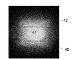
- FIG. 1B shows a case where a plurality of LED elements having the shape shown in FIG. 1A are provided, and the light emitted from each LED element is condensed on a predetermined incident surface via the first optical system and the second optical system. It is the photograph of the image on the said entrance plane when. In the photograph of FIG. 1B, the presence of a dark region is confirmed in part, but when compared with the drawing of FIG. 1A, this dark region corresponds to the position of the electrode portion 42, that is, the position of the non-light emitting region. I understand.
- each LED element having the same size and shape is used, and the wiring pattern provided in each LED element is also the same.
- the light emitted from the plurality of LED elements configured with the same wiring pattern is condensed through the first optical system and the second optical system, the light from the light emitting region is reflected on the condensed surface.
- the intensity of the angle component possessed is increased, and the intensity of the angle component possessed by light (weak light) from the non-light emitting region is decreased.
- an illuminance distribution is generated on the condensed surface.
- FIG. 1B it is considered that the bright area and the dark area exist because of the above reason.
- the plurality of LED elements are arranged so that there are a plurality of types of relative positions of the light emitting area and the non-light emitting area with respect to the optical axis of the collimating lens.
- the angle at which low-intensity light emitted from the non-light-emitting region of a certain LED element is incident on a predetermined incident surface via the first optical system and the second optical system, and the other LED element
- the angle at which the high-intensity light emitted from the light emitting region is incident on the predetermined incident surface via the first optical system and the second optical system can be made the same. That is, the difference in light intensity according to the incident angle can be reduced on the incident surface. Thereby, the illuminance variation on the incident surface is improved, and the uniformity of the illuminance distribution is enhanced.
- the illuminance can be made uniform, so that exposure unevenness can be suppressed.
- a specific first configuration is as follows.
- the plurality of LED elements are: Arranged on a predetermined first plane, When the intersection of the optical axis of the collimating lens corresponding to each of the plurality of LED elements and the first plane is used as a reference point, the center of the LED element on the first plane is relative to the reference point.
- the positions are arranged so that there are a plurality of types.
- a specific second configuration is as follows.
- the plurality of LED elements are: Arranged on a predetermined first plane, When the intersection of the optical axis of the collimating lens corresponding to each of the plurality of LED elements and the first plane is a reference point, a predetermined measurement point other than the center of the LED element on the first plane These are arranged so that there are a plurality of types of relative positions with respect to the reference point.
- a plurality of LED elements may be arranged by combining the first configuration and the second configuration.
- all the relative positions of the centers of the LED elements on the first plane with respect to the reference point may coincide with each other.
- the centers of the LED elements on the first plane may all coincide with the reference point.
- a method is adopted in which a plurality of LED elements are configured so that there are a plurality of types of wiring pattern shapes, or a plurality of types of LED element shapes and dimensions are present. obtain.
- the light source device includes a light guide member having an incident surface disposed at a focal position of the second optical system, and the light guide member transmits light incident from the incident surface to an inner surface.
- the optical member may be an optical member that leads to the exit surface while repeating reflection.
- This light guide member can be composed of, for example, a rod integrator.
- a light source device with improved uniformity of illuminance distribution on the irradiation surface is realized while suppressing a decrease in luminance.
- FIG. 1A It is a schematic diagram when an LED element is seen from the upper surface. It is the photograph of the image on the surface which condensed the light inject
- FIG. It is drawing which expanded a part of FIG. It is drawing which expanded a part of FIG. It is drawing which expanded a part of FIG. It is drawing which shows typically the optical system of the light source device of 2nd embodiment. It is drawing which shows the structure of an exposure apparatus typically. It is drawing which shows typically a mode when the light source part side is seen to a Z direction from between the 1st optical system and the 2nd optical system in the light source device of another embodiment. It is drawing which shows typically a part of structure of the conventional light source device.
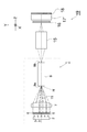
- FIG. 2 is a drawing schematically showing an optical system of the light source device of the first embodiment.
- the light source device 1 includes a light source unit 2, a first optical system 5, a second optical system 7, and a third optical system 8.
- the light source unit 2 includes a plurality of LED elements 3.
- Each of the plurality of LED elements 3 has a structure as shown in FIG. 1A, for example.
- Each LED element 3 is arranged on a predetermined plane.
- the first optical system 5 is an optical system that collimates the light emitted from the plurality of LED elements 3, and is configured by arranging a plurality of collimating lenses 6 corresponding to the LED elements 3.
- the second optical system 7 is an optical system that condenses the light emitted from the first optical system 5 at the focal point 7f of the second optical system 7.
- the third optical system 8 is arranged so that the incident surface 8a is positioned at the focal point 7f of the second optical system 7.
- “arranged at the focal position” means that the lens is moved by a distance within ⁇ 10% in the direction parallel to the optical axis 11 with respect to the focal distance, in addition to the case where it completely coincides with the focal position. It is assumed that the concept includes the determined position.
- the optical axis 11 in FIG. 2 is an axis orthogonal to the incident surface 8a of the third optical system 8.
- the third optical system 8 may be configured by any optical system as long as it has an optical surface 8a on which the light collected by the second optical system 7 is incident. .
- a direction parallel to the optical axis 11 is defined as a Z direction, and a plane orthogonal to the Z direction is described as an XY plane.
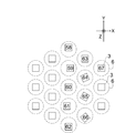
- FIG. 3 is a drawing schematically showing a state when the light source unit 2 side is viewed in the Z direction (the optical axis 11 direction) from between the first optical system 5 and the second optical system 7.
- the light source device 1 in the present embodiment has a plurality of LED elements 3 regularly arranged on a predetermined plane (here, XY plane).
- the collimating lens 6 is disposed at a position facing the Z direction.
- each LED element 3 constituting the outer edge portion forms a regular hexagon, and each LED element 3 is arranged aligned in the X direction and the Y direction.
- the present invention is not limited to such an arrangement mode.
- the LED elements 3 are arranged as closely as possible.
- the light emitted from the center of each LED element 3 spreads to the periphery of the exit surface of the collimating lens 6 and then converted into parallel light, as schematically illustrated with light rays. That is, the luminance on the exit surface of the collimating lens 6 is equal to the luminance on each LED element 3.
- the luminance value of the secondary light source constituted by the exit surface side of the collimating lens 6 group that is, the first optical system 5 is the amount of the gap. Only drops.
- the adjacent collimating lenses 6 are closely arranged in a regular hexagonal shape.
- the collimating lens 6 is configured such that the area of the incident surface 6 a is larger than the area of the light emitting surface of the corresponding LED element 3.
- the LED element 60 is arranged so that the center thereof coincides with the optical axis of the corresponding collimating lens 6.
- the center of the LED element 59 is displaced in the + X direction with respect to the optical axis of the corresponding collimating lens 6.
- the LED element 58 is disposed such that the center thereof is deviated in the + Y direction with respect to the optical axis of the corresponding collimating lens 6.
- the center of the LED element 61 is deviated in the ⁇ X direction with respect to the optical axis of the corresponding collimating lens 6.
- the center of the LED element 62 is deviated in the ⁇ Y direction with respect to the optical axis of the corresponding collimating lens 6. Similar to the LED element 60, the LED element 63 is arranged so that its center coincides with the optical axis of the corresponding collimating lens 6.
- the LED element 3 displayed as the light source unit 2 in FIG. 2 corresponds to the LED elements 58 to 62.
- FIG. 4 is an enlarged view of a part of FIG. 3, and more specifically, LED elements 59 and 60.
- Each of the LED elements 59 and 60 includes a light emitting region 25 and a non-light emitting region 26 having the same shape.
- the light emitting region 25 corresponds to, for example, the light extraction portion 41 shown in FIG. 1A
- the non-light emitting region 26 corresponds to, for example, the electrode portion 42 shown in FIG. 1A.
- the LED element 60 is arranged so that its center C60 coincides with the reference point O.
- the center C59 of the LED element 59 is displaced from the reference point O in the + X direction.
- the light emitted from the LED element 3 enters the corresponding collimator lens 6, is converted into parallel light, and is guided to the second optical system 7.
- the coordinate on the incident surface 6a of the collimating lens 6 is described as ⁇
- the coordinate on the incident surface 6a of the second optical system 7 is described as ⁇ . If there is an intensity difference in the incident light according to the coordinates ⁇ on each incident surface 6a, the light remains with the intensity difference at the position of the coordinate ⁇ on the incident surface 7a corresponding to the coordinate ⁇ . Is incident. Then, light having an intensity difference corresponding to the coordinate ⁇ is incident on the incident surface 8a of the third optical system 8 at an incident angle ⁇ corresponding to the coordinate ⁇ on the incident surface 7a.
- the incident surface 8a of the third optical system 8 differs according to the incident angle ⁇ converted from the coordinate ⁇ . Intense light is incident.
- the LED elements 60 and 63 have a common relative positional relationship with respect to the reference point O. Therefore, as shown in FIG. 4, the reference point O is located in the light emitting region 25, and another point P is located in the non-light emitting region 26. That is, the light emitted from the reference point O of the LED element 60 and the light emitted from the reference point O of the LED element 63 are both in a high intensity state at an incident angle ⁇ O corresponding to the reference point O. The light enters the incident surface 8 a of the third optical system 8.
- the light emitted from the point P of the LED element 60 and the light emitted from the point P of the LED element 63 are both in a low intensity state, and the third optical at an incident angle ⁇ P corresponding to the point P.
- the light enters the incident surface 8 a of the system 8.
- the incident light is incident on the incident surface 8a of the third optical system 8 at an incident angle ⁇ O. that while the intensity of the light L O is increased by the number of LED elements 3, the light L P to be incident at an angle theta P, since only low light intensity is being collected, the intensity of the light L P is It is significantly lower than the intensity of light L 2 O.
- the above contents are reduced to the relationship between the light emitted from the point set located in the light emitting area 25 and the light emitted from the point set located in the non-light emitting area 26. That is, when all the LED elements 3 have the same relative positional relationship with respect to the reference point O as that of the LED element 60, the light intensity varies depending on the incident angle ⁇ on the incident surface 8a of the third optical system 8. Occurs. As a result, illuminance variation (illuminance distribution) occurs on the incident surface 8a. The photograph shown in FIG. 1B matches this verification content.
- At least some of the LED elements 3 among the plurality of LED elements 3 are different in relative positional relationship with the corresponding collimating lens 6.
- the center of the LED element 59 is displaced in the + X direction with respect to the optical axis of the corresponding collimating lens 6.
- the relative positional relationship with the lens 6 is different.
- the point P is located in the non-light emitting region 26, but in the LED element 59, the relative position from the reference point O is the same.
- the point P is located in the light emitting region 25.
- the light emitted from the point P of the LED element 60 is incident on the incident surface 8a of the third optical system 8 with the incident angle ⁇ P in a low intensity state.
- the light emitted from the point P of the element 59 enters the incident surface 8a with the incident angle ⁇ P in a high intensity state.
- the LED elements 3 are arranged such that the relative position of the light emitting area 25 and the relative position of the non-light emitting area 26 with respect to the reference point O are different from each other.
- the light intensity difference corresponding to the incident angle ⁇ on the incident surface 8a of the three optical system 8 can be reduced. Thereby, the illuminance variation on the incident surface 8a of the third optical system 8 is improved as compared with the conventional configuration.
- FIG. 5 is another drawing showing the arrangement method of the LED elements 3, which is displayed in accordance with FIG.
- the LED elements 58 to 62 shown in FIG. 3 are arranged so that the relative positions of the respective centers with respect to the optical axis of the corresponding collimating lens 6 are different from each other. As described above, such an arrangement is made with the intention of making the relative position of the light emitting region 25 relative to the reference point O and the relative position of the non-light emitting region 26 different from each other. However, if the above contents are realized, the arrangement of the plurality of LED elements 3 is not limited to the example of FIG.
- the optical axis of the corresponding collimating lens 6 coincides with the center of each LED element (64, 65).
- the LED elements 64 and 65 are both in a state in which the LED element 60 is rotated around the optical axis of the corresponding collimating lens 6 on the XY plane.
- the relative positional relationship with respect to the optical axis of the collimating lens 6 corresponding to each of the LED elements 64 and 65 is different.
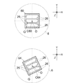
- FIG. 6 is an enlarged view of a part of FIG. 5, and specifically shows a vicinity where the LED element 60 is disposed and a vicinity where the LED element 64 is disposed.
- the LED element 64 corresponds to a state in which the LED element 60 is rotated by 25 ° counterclockwise around the reference point O.
- the center C ⁇ b> 64 of the LED element 64 coincides with the reference point O in the same manner as the center C ⁇ b> 60 of the LED element 60.
- the situation is different from the LED element 59 in which the center C59 is arranged at a position different from the center C60 of the LED element 60.
- a certain point Q on the LED element 60 is located in the non-light emitting region 26, but in the LED element 64, the relative position from the reference point O is the same.
- a certain point Q is located in the light emitting region 25.
- the relative position of the light emitting region 25 and the non-light emitting region 26 with respect to the reference point O can be made different by rotating the LED element 3 itself without changing the center position of the LED element 3.
- the illuminance variation on the incident surface 8a of the third optical system 8 is improved.
- the light emitting region with respect to the reference point O can also be obtained by changing the relative position of the predetermined measurement point other than the center with respect to the reference point O on the plane on which the LED element 3 is arranged. That is, the relative position of 25 and the relative position of the non-light emitting region 26 can be made different.
- the measurement point may be a point determined by a predetermined rule.
- the measurement point may be each vertex of the side constituting the outer periphery of the LED element 3 or each center point of the side. It can also be the point Q.
- the LED element 60 may be rotated with the reference point O as the center and further displaced at the center position.
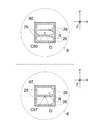
- FIG. 7 is another drawing in which a part of FIG. 5 is enlarged and displayed in detail, showing the vicinity where the LED element 60 is arranged and the vicinity where the LED element 67 is arranged. Similar to the LED element 60, the center of the LED element 67 coincides with the optical axis of the corresponding collimating lens 6. Further, the relative positional relationship of the sides constituting each LED element (60, 67) with respect to the reference point O on the XY plane is the same. However, as shown in FIG. 7, the LED element 60 and the LED element 67 are formed so that the shapes of the light emitting region 25 and the non-light emitting region 26 are different from each other. More specifically, the LED elements 60 and 67 have different electrode portions 42 (see FIG. 1B).
- a certain point R on the LED element 60 is located in the non-light emitting region 26, but in the LED element 67, the point R having the same relative position from the reference point O is the same. Is located in the light emitting region 25.
- the light emitted from the point R of the LED element 60 is incident on the incident surface 8a of the third optical system 8 at an incident angle ⁇ R in a low intensity state.
- the light emitted from the point R is incident on the incident surface 8a at the incident angle ⁇ R in a high intensity state.
- the relative position of the light emitting region 25 and the non-light emitting region 26 with respect to the reference point O can also be obtained by configuring at least some of the plurality of LED elements 3 with different configurations of the electrode portions 42. Can be different. Thereby, the illuminance variation on the incident surface 8a of the third optical system 8 is improved.
- the plurality of LED elements 3 are the ones whose center positions are deviated with respect to the LED elements 60 (LED elements 58, 59, 61, 62, 66), and the reference with respect to the LED elements 60.
- a state in which all of the elements rotated around the point (LED elements 64, 65, 66) and the one in which the shape pattern of the electrode part 42 is changed with respect to the LED element 60 (LED element 67) are mixed. It was shown. However, this is for convenience of explanation.
- the plurality of LED elements 3 only need to include at least one aspect of the configurations exemplified above.
- FIG. 8 is a drawing schematically showing an optical system of the light source device of the second embodiment.
- the light source device 1 shown in FIG. 8 differs from the first embodiment in that a rod integrator 9 is arranged as the third optical system 8.
- the rod integrator 9 is arranged so that the incident surface 9a is positioned at the focal point 7f of the second optical system 7.
- the rod integrator 9 is configured to propagate light along the longitudinal direction (here, the Z direction) while maintaining the angle at which the light incident on the incident surface 9a travels by totally reflecting the light on the inner surface. It is configured. That is, the rod integrator 9 has a function of making the illuminance distribution on the exit surface 9b uniform while maintaining the angle of the light incident on the entrance surface 9a.
- the illuminance variation of the light collected by the second optical system 7 is suppressed for the same reason as described in the first embodiment. Therefore, by making this light incident on the incident surface 9a of the rod integrator 9 as in the present embodiment, light with significantly improved illuminance distribution uniformity can be obtained on the exit surface 9b of the rod integrator 9.
- the rod integrator 9 guides the light incident on the incident surface 9a to the exit surface 9b while repeating total reflection on the side surface, thereby having a function of making the illuminance distribution of the light on the exit surface 9b uniform.
- a light member includes, for example, a columnar member made of a light-transmitting material such as glass or resin, a hollow member whose inner surface is formed of a reflecting mirror, and the like. The latter configuration is sometimes called a light tunnel.
- the light guide member may be configured by dividing a plurality of optical paths in a direction parallel to the optical axis.
- FIG. 9 is a drawing schematically showing the configuration of the exposure apparatus.
- the exposure apparatus 19 shown in FIG. 9 includes the light source device 1 of the second embodiment shown in FIG.
- the exposure apparatus 19 includes a projection optical system 15 and a mask 16 at the subsequent stage of the rod integrator 9, and a projection lens 17 as necessary.
- a mask 16 is placed at a position projected by the projection optical system 15, and a photosensitive substrate 18 to be a target for printing a pattern image of the mask 16 is placed after the mask 16.
- the light emitted from the light source unit 2 is collected by the second optical system 7 and then the light of the rod integrator 9 as light with suppressed illuminance variation (light with uniform illuminance distribution). It is incident on the incident surface 9a. Then, while this light travels through the rod integrator 9, total reflection is repeated on the inner surface, so that the light is guided onto the exit surface 9 b as light with suppressed illuminance variation, and this light is projected onto the projection optical system 15. Is irradiated.
- the projection optical system 15 projects the pattern image of the mask 16 onto the photosensitive substrate 57 directly or via the projection lens 17.
- the exposure apparatus 19 includes the light source device 1 according to the second embodiment, so that exposure is performed using light with significantly improved illuminance variation compared to the prior art, that is, light with significantly improved illuminance distribution uniformity. Exposure unevenness can be suppressed.
- the exposure apparatus 19 may adopt a configuration in which light emitted from the third optical system 8 configured by an optical system other than the rod integrator 9 is incident on the projection optical system 15. .
- the arrangement shape of the LED elements 3 is not limited to that described with reference to FIGS. 3 and 5.
- the interval between adjacent LED elements 3 may be wider than the configuration of the above embodiment, or a plurality of LED elements 3 may be randomly arranged.
- the plurality of LED elements 3 by arranging the plurality of LED elements 3 as densely as possible, an effect of further reducing the illuminance variation on the incident surface 8a of the third optical system 8 can be obtained. This will be described below.
- the second optical system 7 By arranging the plurality of LED elements 3 and the corresponding collimating lenses 6 as illustrated in FIG. 3 or FIG. 5, many LED elements 3 can be concentrated in a limited area. Thereby, the emitted light from many LED elements 3 can be condensed by the second optical system 7. As shown in FIG. 2, for example, a light beam 20a formed by light emitted from a certain LED element 3 (here, LED element 58) through the second optical system 7 and another LED element 3 (here, LED element 59). The distance d between the light emitted from the light beam 20b formed through the second optical system 7 can be made as short as possible. That is, the light incident on the incident surface 8a of the third optical system 8 can be made dense. As a result, it is possible to condense the light having no missing angular component on the incident surface 8 a of the third optical system 8.
- each LED element 3 constituting the outer edge portion forms a substantially square shape, and each LED element 3 is arranged in alignment in the X direction and the Y direction.
- each LED element 3 and each collimating lens 6 can be arranged densely. Even in the case where the LED element 3 is arranged in this way, it is possible to further condense light having no missing angular component on the incident surface 8a of the third optical system 8.
- the traveling direction of light may be changed by appropriately arranging, for example, a reflection optical system between the light source unit 2 and the third optical system 8.
- the plane on which the plurality of LED elements 3 are arranged and the incident surface 8a of the third optical system 8 do not necessarily exist on a parallel plane, but for the same reason as described above, On the incident surface 8a of the three optical system 8, light with reduced illuminance variation is obtained.
- the third optical system 8 is described as being disposed at the focal position of the second optical system 7.
- the irradiation object is directly placed at the focal position of the second optical system 7. May be installed.
- Light source device 2 Light source unit 3: LED element 5: First optical system 6: Collimating lens 6a: Collimating lens incident surface 7: Second optical system 7a: Second optical system incident surface 7f: Second optical system 8: Third optical system 8a: Entrance surface of third optical system 11: Optical axis 15: Projection optical system 16: Mask 17: Projection lens 18: Photosensitive substrate 19: Exposure apparatus 25: Light emitting area 26: Non-light emitting Area 40: LED element 41: Light extraction part 42: Electrode part 43: Element covering part 58-67: LED element 100: Light source 101, 102: LED element 103: Collimating lens 104: Fly eye lens 110: Fly eye lens One lens 121 constituting a's: lens 110 of the incident surface 122: the exit surface of the lens 110 IM101: image of the LED element 101 IM102: image of the LED element 102
Landscapes
- Physics & Mathematics (AREA)
- General Physics & Mathematics (AREA)
- Optics & Photonics (AREA)
- Exposure And Positioning Against Photoresist Photosensitive Materials (AREA)
- Microscoopes, Condenser (AREA)
Abstract
複数のLED素子を含み、輝度の低下を抑制した光源装置を実現する。 光源装置は、複数のLED素子と、複数のLED素子から射出された光をそれぞれコリメートする複数のコリメートレンズを含む第一光学系と、第一光学系から射出された光を集光する第二光学系とを備える。複数のLED素子は、それぞれに対応するコリメートレンズの光軸の方向から見たときに、発光領域と非発光領域を有し、それぞれに対応するコリメートレンズの光軸を基準としたときの発光領域の相対位置及び非発光領域の相対位置が複数種類存在するように配置されている。
Description
本発明は、光源装置に関し、特に、複数のLED素子を備えた光源装置に関する。また、本発明は、このような光源装置を含む露光装置に関する。
従来、光を用いた微細加工に露光装置が利用されている。近年では、露光技術は種々の分野で展開されており、微細加工の中でも比較的大きなパターンの作製や三次元的な微細加工に利用されている。より具体的には、例えばLEDの電極パターンの作製や、加速度センサーに代表されるMEMS(Micro Electro Mechanical Systems)の製造工程などに露光技術が利用されている。
これらの露光技術において、以前から、光源として輝度の高い放電ランプが用いられていた。しかし、近年の固体光源技術の進歩に伴い、複数のLED素子が配置されたものを光源として利用することが検討されている。このような技術として、例えば特許文献1には、複数のLED素子からなるユニットを光源とし、この光源とマスクの間にフライアイレンズが配置された露光装置が開示されている。
LED素子は、露光用の光源としては一チップ当たりの放射光束が少ない。このため、露光用の光源装置として使用するためには、複数のLED素子からの射出光をできる限り集める必要がある。このためには、光源として配置されるLED素子の個数を増やす必要がある。
上記特許文献1に開示された光源装置の構成を、図11を参照して説明する。図11(a)は、この光源装置の一部分を模式的に示した図面である。図11(a)に示すように、この光源装置は、複数のLED素子(101,102,…)を含む光源100、コリメートレンズ103、及びフライアイレンズ104を含んで構成される。図11(b)は、図11(a)の一部拡大図である。
LED素子101は光軸の中心に位置しており、LED素子102は光源100の周縁部に位置している。図11に示される光線L1は、LED素子101からの放射光のうち、フライアイレンズ104に含まれる一つのレンズ110の入射面121に入射される光である。同様に、光線L2は、LED素子102からの放射光のうち、フライアイレンズ104に含まれる一つのレンズ110の入射面121に入射される光である。
光軸の中心に位置するLED素子101から射出される光線L1は、レンズ110に対して、光軸に平行に入射される。一方、光軸から離れた位置に配置されたLED素子102から射出される光線L2は、レンズ110に対して、光軸に対して角度を有して入射される。これらの光は、レンズ110の射出面122でそれぞれ結像する(IM101,IM102)。図11(c)は、レンズ110の射出面122に結像された状態を模式的に示す図面である。
射出面122から射出される光が後段の光学系(不図示)に入射されることで、この光が利用される。つまり、射出面122は二次光源となる。この二次光源の輝度は、個々のLED素子(101,102,…)の輝度に、LED像(IM101,IM102,…)の総面積を乗じ、射出面122の面積で除した値となる。すなわち、二次光源として機能する射出面122の輝度をできるだけ高くするためには、LED像の総面積と射出面122の面積をなるべく一致させる必要がある。このためには、LED素子(101,102,…)をなるべく隙間なく並べることが必要である。
しかし、図11に示すように、複数のLED素子(101,102,…)を配置して光源100を構成する場合、各LED素子(101,102,…)に電流を供給するための信号線やスイッチング素子などの周辺回路が必要となる。このため、現実的には、LED素子(101,102,…)を隙間なく並べることができない。この結果、従来の構成によれば、二次光源(図11の構成であればフライアイレンズ104の射出面)の輝度が低下してしまう。
このような課題に鑑み、本発明は、複数のLED素子を含み、輝度の低下を抑制した光源装置を実現することを目的とする。また、本発明は、このような光源装置を含む露光装置を実現することを目的とする。
本発明の光源装置は、
複数のLED素子と、
前記複数のLED素子から射出された光をそれぞれコリメートする複数のコリメートレンズを含む第一光学系と、
前記第一光学系から射出された光を集光する第二光学系とを備え、
前記複数のLED素子は、
それぞれに対応する前記コリメートレンズの光軸の方向から見たときに、発光領域と非発光領域を有し、
それぞれに対応する前記コリメートレンズの光軸を基準としたときの前記発光領域の相対位置及び前記非発光領域の相対位置が複数種類存在するように配置されていることを特徴とする。
複数のLED素子と、
前記複数のLED素子から射出された光をそれぞれコリメートする複数のコリメートレンズを含む第一光学系と、
前記第一光学系から射出された光を集光する第二光学系とを備え、
前記複数のLED素子は、
それぞれに対応する前記コリメートレンズの光軸の方向から見たときに、発光領域と非発光領域を有し、
それぞれに対応する前記コリメートレンズの光軸を基準としたときの前記発光領域の相対位置及び前記非発光領域の相対位置が複数種類存在するように配置されていることを特徴とする。
前述したように、一つのLED素子から射出される光は、ランプに比べて輝度が小さい。このため、例えば露光装置用の光源など、多くの光を必要とする用途の光源に利用されることを想定した場合には、なるべく輝度を落とすことなく、多くのLED素子の光を集めることが重要となる。
ところで、LED素子は、電源供給のための配線パターンが不可欠であるため、「発明が解決しようとする課題」の項で上述したように、LED素子自体を完全に密接して配置することができない。つまり、複数のLED素子を配置するに際しては、隣接するLED素子同士に一定の間隔を空けざるを得ない。この間隔を形成する領域は、光を射出しない領域(非発光領域)を構成する。このため、単に複数のLED素子を配置し、各LED素子からの射出光を集光したとしても、非発光領域が不可避的に生じてしまう。よって、複数のLED素子から射出された光を単に集光しただけでは、照射面での輝度の低下を招いてしまう。
上記構成によれば、複数のLED素子から射出された光を、第一光学系においてコリメートした後に、集光している。これにより、第一光学系から射出された光は、LED素子から射出された直後の時点に比べて、輝度を維持したまま、光軸に直交する平面上において面積の広い光束を構成する。これにより、各LED素子から射出された光束同士の間隔を狭めることができ、非発光領域の少ない光源が構成される。これにより、従来よりも輝度の高い光源装置が実現される。
更に、上記の構成によれば、照射面における照度分布を均一化できるという第二の効果も実現される。この点につき説明する。図1Aは、LED素子を上面から見たときの模式図である。図1Aに示すLED素子40は、光取り出し部41、電極部42、及び素子被覆部43を備えている。光取り出し部41は、通常、半導体層で構成されており、発光領域を構成する。電極部42は、光を透過しない導電性材料で構成されており、非発光領域を構成する。
図1Bは、図1Aに示す形状を有するLED素子を複数備えた場合において、各LED素子からの射出光を、第一光学系及び第二光学系を介して所定の入射面上に集光させたときの、当該入射面上における像の写真である。図1Bの写真において、一部分に暗い領域の存在が確認されるが、図1Aの図面と照らし合わせると、この暗い領域が電極部42の位置、すなわち非発光領域の位置に対応していることが分かる。
通常、光源に複数のLED素子を配置させる場合においては、各LED素子は同一の寸法及び形状を示すものが使用され、各LED素子が備える配線パターンも同一である。同一の配線パターンで構成された複数のLED素子から射出された光を、第一光学系及び第二光学系を介して集光した場合、集光された面上において、発光領域からの光が有する角度成分の強度は高くなり、非発光領域からの光(弱い光)が有する角度成分の強度は低くなる。結果として、集光された面上において照度分布が生じる。図1Bの写真において、明るい領域と暗い領域が存在しているのは、上記の理由によるものと考えられる。
従って、図1Bに示されるような照度分布を有した光を、露光用の光として、例えばワークに照射した場合、ワーク面に露光ムラが生じる可能性がある。
しかし、上記光源装置の構成によれば、コリメートレンズの光軸に対する発光領域の相対位置及び非発光領域の相対位置が複数種類存在するように、複数のLED素子が配置される。これにより、あるLED素子の非発光領域から射出された強度の低い光が、第一光学系及び第二光学系を介して所定の入射面に入射される際の角度と、別のLED素子の発光領域から射出された強度の高い光が、第一光学系及び第二光学系を介して所定の入射面に入射される際の角度とを、同じにすることができる。つまり、入射面上において、入射角度に応じた光の強度差を小さくすることができる。これにより、入射面上における照度バラツキが改善され、照度分布の均一性が高められる。
つまり、上記の構成によれば、光源部にLED素子を用いた場合においても、高い輝度を実現すると共に、更に照度バラツキを抑制することができる。よって、高輝度の光が要求される、露光用の光源として利用することができる。また、この構成によれば、照度の均一化も図られるため、露光ムラを抑制することもできる。
上記構成を実現するための具体的な方法は、種々採用され得る。
具体的な第一の構成は、以下の通りである。
前記複数のLED素子は、
所定の第一平面上に配置されており、
当該複数のLED素子のそれぞれに対応する前記コリメートレンズの光軸と前記第一平面との交点を基準点としたときに、前記第一平面上における当該LED素子の中心の、前記基準点に対する相対位置が、複数種類存在するように配置されている。
前記複数のLED素子は、
所定の第一平面上に配置されており、
当該複数のLED素子のそれぞれに対応する前記コリメートレンズの光軸と前記第一平面との交点を基準点としたときに、前記第一平面上における当該LED素子の中心の、前記基準点に対する相対位置が、複数種類存在するように配置されている。
具体的な第二の構成は、以下の通りである。
前記複数のLED素子は、
所定の第一平面上に配置されており、
当該複数のLED素子のそれぞれに対応する前記コリメートレンズの光軸と前記第一平面と交点を基準点としたときに、前記第一平面上における当該LED素子の前記中心以外の所定の計測点の、前記基準点に対する相対位置が、複数種類存在するように配置されている。
前記複数のLED素子は、
所定の第一平面上に配置されており、
当該複数のLED素子のそれぞれに対応する前記コリメートレンズの光軸と前記第一平面と交点を基準点としたときに、前記第一平面上における当該LED素子の前記中心以外の所定の計測点の、前記基準点に対する相対位置が、複数種類存在するように配置されている。
なお、複数のLED素子が、上記第一の構成と第二の構成とが組み合わされて配置されていても構わない。
また、上記第二の構成において、前記第一平面上における当該LED素子の中心の、前記基準点に対する相対位置が全て一致しているものとしても構わない。この場合において、前記第一平面上における当該LED素子の中心が、全て前記基準点に一致しているものとしても構わない。
その他の具体的な構成としては、複数のLED素子を、配線パターンの形状が複数種類存在するように構成したり、LED素子の形状や寸法自体を複数種類存在するように構成する方法が採用され得る。
前記光源装置は、上記構成に加えて、入射面が前記第二光学系の焦点位置に配置された導光部材を備え、前記導光部材は、前記入射面から入射された光を、内側面で反射を繰り返させながら射出面へと導く光学部材であるものとしても構わない。この導光部材は、例えばロッドインテグレータで構成されることができる。
導光部材内において入射された光がそれぞれ反射を繰り返すことで、導光部材内で色々な角度成分及び位置成分の光が混ざり合うため、導光部材の射出面上においては、その入射面よりも照度が均一化される。よって、この構成によれば、更に照度が均一な光を生成することができ、この光を露光用に利用した場合には露光ムラを抑制することができる。
本発明によれば、複数のLED素子を備える構成において、輝度の低下を抑制しながらも、照射面上において照度分布の均一性を高めた光源装置が実現される。
以下、本発明の光源装置及び露光装置につき、図面を参照して説明する。なお、各図における寸法比は、実際の寸法比と必ずしも一致していない。
[第一実施形態]
図2は、第一実施形態の光源装置の光学系を模式的に示す図面である。光源装置1は、光源部2と、第一光学系5と、第二光学系7と、第三光学系8を備える。
図2は、第一実施形態の光源装置の光学系を模式的に示す図面である。光源装置1は、光源部2と、第一光学系5と、第二光学系7と、第三光学系8を備える。
光源部2は、複数のLED素子3を含む。複数のLED素子3は、それぞれ、例えば図1Aに示したような構造を有している。各LED素子3は、所定の平面上に配置されている。
第一光学系5は、複数のLED素子3から射出された光をそれぞれコリメートする光学系であり、各LED素子3に対応して複数のコリメートレンズ6が配置されて構成されている。
第二光学系7は、第一光学系5から射出された光を、第二光学系7の焦点7fに集光する光学系である。
第三光学系8は、その入射面8aが、第二光学系7の焦点7fの位置になるように配置されている。ただし、本明細書では、「焦点位置に配置する」とは、完全に焦点の位置に一致する場合の他、焦点距離に対して光軸11に平行な方向に±10%以内の距離だけ移動した位置を含む概念であるものとする。なお、図2における光軸11とは、第三光学系8の入射面8aに対して直交する軸としている。本実施形態において、第三光学系8は、第二光学系7によって集光された光が入射される面8aを有する光学系であれば、どのような光学系で構成されていても構わない。
なお、以下では、光軸11に平行な方向をZ方向とし、このZ方向に直交する平面をXY平面として説明する。
図3は、第一光学系5と第二光学系7との間から、Z方向(光軸11方向)に光源部2側を見たときの様子を模式的に示す図面である。本実施形態における光源装置1は、一例として、図3に示されるように、複数のLED素子3は、所定の平面(ここではXY平面)上に規則的に配置されており、各LED素子3に対してZ方向に対向する位置にコリメートレンズ6が配置されている。図3の例では、外縁部を構成する各LED素子3が正六角形を構成し、且つ、各LED素子3がX方向及びY方向に整列して配置されているが、本発明は、このような配置態様に限定されるものではない。
ただし、第三光学系8の入射面8aに集光される光の輝度をできるだけ高くするためには、各LED素子3をできる限り密接して配置するのが好ましい。図2において、模式的に光線を図示しているように、各LED素子3の中心から射出された光が、コリメートレンズ6の射出面の周囲まで拡がった後、平行光に変換される。すなわち、コリメートレンズ6の射出面上での輝度は、各LED素子3上における輝度に等しい。このため、隣接するコリメートレンズ6間に隙間が生じていると、コリメートレンズ6群(すなわち、第一光学系5)の射出面側によって構成される二次光源の輝度値が、この隙間の分だけ低下する。よって、各LED素子3の輝度をできるだけ維持させるためには、隣接するコリメートレンズ6をなるべく密着させるのが好ましい。かかる観点から、本実施形態では、各コリメートレンズ6を正六角形状に密接配置している。コリメートレンズ6は、入射面6aの面積が、対応するLED素子3の発光面の面積よりも大きくなるように構成されている。
図3では、各LED素子3のうち、説明の便宜上、符号58~63を付した6つのLED素子3を採り上げて説明する。図3の例では、LED素子60は、その中心が、対応するコリメートレンズ6の光軸に一致するように配置されている。LED素子59は、その中心が、対応するコリメートレンズ6の光軸に対して+X方向に偏位して配置されている。LED素子58は、その中心が、対応するコリメートレンズ6の光軸に対して+Y方向に偏位して配置されている。LED素子61は、その中心が、対応するコリメートレンズ6の光軸に対して-X方向に偏位して配置されている。LED素子62は、その中心が、対応するコリメートレンズ6の光軸に対して-Y方向に偏位して配置されている。LED素子63は、その中心が、LED素子60と同様に、対応するコリメートレンズ6の光軸に一致するように配置されている。
図2において光源部2として表示されているLED素子3は、LED素子58~62に対応している。
図4は、図3の一部を拡大して表示した図面であり、詳細にはLED素子59及び60を表示した図面である。LED素子59及び60は、いずれも同形状の発光領域25及び非発光領域26を備えている。発光領域25は、例えば図1Aに示す光取り出し部41に対応し、非発光領域26は、例えば図1Aに示す電極部42に対応する。
図4では、各LED素子(59,60)に対応して配置されているコリメートレンズ6の光軸と、各LED素子(59,60)が配置された平面(XY平面)との交点を点Oとして表示している。以下では、この点Oを「基準点O」と呼ぶことがある。
図4の例では、LED素子60は、その中心C60が、基準点Oに一致するように配置されている。これに対し、LED素子59は、その中心C59は、基準点Oよりも+X方向に偏位して配置されている。
図2に示すように、LED素子3から射出された光は、対応するコリメートレンズ6に入射された後、平行光に変換されて第二光学系7へと導かれる。ここで、説明の便宜のため、コリメートレンズ6の入射面6a上における座標をαと記載し、第二光学系7の入射面6a上における座標をβと記載する。各入射面6a上の座標αに応じて、入射された光に強度差が存在する場合、この座標αに応じた、入射面7a上の座標βの位置に、前記強度差を有したまま光が入射される。そして、第三光学系8の入射面8aに対しては、入射面7a上の座標βに応じた入射角度θで、座標βに応じた強度差を有した光が入射される。
つまり、コリメートレンズ6の入射面6a上における座標αに応じて光の強度差がある場合、第三光学系8の入射面8aには、この座標αが変換された入射角度θに応じて異なる強度の光が入射される。
図3に戻り、LED素子60及び63は、基準点Oに対する相対的な位置関係が共通である。このため、図4に示すように、基準点Oは発光領域25内に位置しており、別の点Pは非発光領域26内に位置している。つまり、LED素子60の基準点Oから射出された光と、LED素子63の基準点Oから射出された光とは、共に強度が高い状態で、当該基準点Oに応じた入射角度θOで第三光学系8の入射面8aに入射される。同様に、LED素子60の点Pから射出された光と、LED素子63の点Pから射出された光は、共に強度が低い状態で、当該点Pに応じた入射角度θPで第三光学系8の入射面8aに入射される。
つまり、仮に、全てのLED素子3が、基準点Oに対する相対的な位置関係がLED素子60と共通であるとすれば、第三光学系8の入射面8aにおいて、入射角度θOで入射される光LOの強度はLED素子3の数だけ高められる一方、入射角度θPで入射される光LPは、強度の低い光が集められているに過ぎないため、光LPの強度は光LOの強度よりも大幅に低下する。
上記の内容は、発光領域25内に位置する点集合から射出された光と、非発光領域26内に位置する点集合から射出された光の関係に帰納される。つまり、全てのLED素子3が、基準点Oに対する相対的な位置関係がLED素子60と共通である場合、第三光学系8の入射面8aでは、入射角度θに応じて光の強度に差が生じる。この結果、入射面8a上において照度バラツキ(照度分布)が生じる。図1Bに示す写真は、この検証内容に合致するものである。
本実施形態の構成では、図3を参照して説明したように、複数のLED素子3のうち、少なくとも一部のLED素子3同士は、対応するコリメートレンズ6との相対的な位置関係が異なるように配置されている。例えば、上述したように、LED素子59は、その中心が、対応するコリメートレンズ6の光軸に対して+X方向に偏位して配置されており、LED素子60との間では、対応するコリメートレンズ6との相対的な位置関係が異なっている。このため、図4に示すように、例えば、LED素子60においては、点Pが非発光領域26内に位置していたが、LED素子59においては、基準点Oからの相対位置が同じである点Pが、発光領域25内に位置している。
このように構成されたとき、LED素子60の点Pから射出された光は、強度が低い状態で入射角度θPを有して第三光学系8の入射面8aに入射されるものの、LED素子59の点Pから射出された光は、強度が高い状態で前記入射角度θPを有して入射面8aに入射される。
つまり、複数のLED素子3のうち、少なくとも一部のLED素子3が、基準点Oに対する発光領域25の相対位置及び非発光領域26の相対位置が相互に異なるように配置されることで、第三光学系8の入射面8a上における入射角度θに応じた光の強度差を小さくすることができる。これにより、従来の構成と比較して、第三光学系8の入射面8a上における照度のバラツキが改善される。
図3の例では、複数のLED素子3のうち、LED素子58、59、61、及び62についてのみ、LED素子60と比較して、基準点Oに対する相対的な位置関係を異ならせるように配置された。しかし、前記相対的な位置関係の種類が多いほど、第三光学系8の入射面8a上における照度バラツキを改善する効果を高めることができる。
図5は、LED素子3の配置方法を示す別の図面であり、図3にならって表示されたものである。
図3に示したLED素子58~62は、対応するコリメートレンズ6の光軸に対する、それぞれの中心の相対位置が相互に異なるように配置されていた。このような配置は、上述したように、基準点Oに対する発光領域25の相対位置及び非発光領域26の相対位置を相互に異ならせることを意図してなされたものである。しかし、前記の内容が実現されていれば、複数のLED素子3の配置態様は、図3の例に限られない。
例えば、図5に示すLED素子64及び65は、LED素子60と同様に、対応するコリメートレンズ6の光軸と、それぞれのLED素子(64,65)の中心が一致している。しかし、LED素子64及び65は、いずれも、XY平面上において、対応するコリメートレンズ6の光軸を中心としてLED素子60を回転させた状態である。これにより、LED素子64及び65は、LED素子60と比較して、それぞれに対応するコリメートレンズ6の光軸に対する相対的な位置関係が異なっている。
図6は、図5の一部を拡大して表示した図面であり、詳細にはLED素子60が配置されている近傍及びLED素子64が配置されている近傍を表示した図面である。図5及び図6の例では、LED素子64は、LED素子60に対して、基準点Oを中心に反時計回りに25°回転させた状態に対応している。このとき、図6に示すように、LED素子64の中心C64は、LED素子60の中心C60と同じく基準点Oに一致している。この点において、図4を参照して上述したように、LED素子60の中心C60と異なる位置に中心C59が配置されているLED素子59とは、事情が異なっている。
図6に示すように配置された場合、例えば、LED素子60上のある点Qは非発光領域26内に位置していたが、LED素子64においては、基準点Oからの相対位置が同じである点Qが、発光領域25内に位置している。このように構成されたとき、LED素子60の点Qから射出された光は、強度が低い状態で入射角度θQで第三光学系8の入射面8aに入射されるものの、LED素子64の点Qから射出された光は、強度が高い状態で前記入射角度θQで入射面8aに入射される。
つまり、LED素子3の中心の位置は変えずに、LED素子3自体を回転させて配置することによっても、基準点Oに対する発光領域25の相対位置及び非発光領域26の相対位置を異ならせることができ、これによって、第三光学系8の入射面8a上における照度バラツキが改善される。この内容をより厳密に記載すれば、LED素子3が配置されている平面上において、中心以外の所定の計測点の、基準点Oに対する相対位置を異ならせることによっても、基準点Oに対する発光領域25の相対位置及び非発光領域26の相対位置を異ならせることができるということになる。ここで、前記の計測点とは、所定の規則で定めた点にすればよく、例えばLED素子3の外周を構成する辺の各頂点とすることもできるし、前記辺の各中央点とすることもできるし、更にいえば前記点Qとすることもできる。
なお、LED素子66のように、LED素子60に対して基準点Oを中心に回転させた上で、更に中心の位置を偏位させて配置させるものとしても構わない。
図7は、図5の一部を拡大して表示した別の図面であり、詳細にはLED素子60が配置されている近傍及びLED素子67が配置されている近傍を表示した図面である。LED素子67は、LED素子60と同様に、その中心が、対応するコリメートレンズ6の光軸と一致している。また、XY平面上において、基準点Oに対する、各LED素子(60,67)を構成する辺の相対的な位置関係も同じである。しかし、図7に示すように、LED素子60とLED素子67は、発光領域25及び非発光領域26の形状が相互に異なるように形成されている。より具体的には、LED素子60と67では、電極部42(図1B参照)の形状が異なっている。
このように配置された場合、例えば、LED素子60上のある点Rは非発光領域26内に位置していたが、LED素子67においては、基準点Oからの相対位置が同じである点Rが、発光領域25内に位置している。このように構成されたとき、LED素子60の点Rから射出された光は、強度が低い状態で入射角度θRで第三光学系8の入射面8aに入射されるものの、LED素子67の点Rから射出された光は、強度が高い状態で前記入射角度θRで入射面8aに入射される。
つまり、複数のLED素子3のうちの少なくとも一部の素子を、電極部42の形状が異なる構成とすることによっても、基準点Oに対する発光領域25の相対位置及び非発光領域26の相対位置を異ならせることができる。これによって、第三光学系8の入射面8a上における照度バラツキが改善される。
なお、図5において、複数のLED素子3には、LED素子60に対して中心の位置を偏位させたもの(LED素子58,59,61,62,66)、LED素子60に対して基準点を中心に回転させたもの(LED素子64,65,66)、及びLED素子60に対して電極部42の形状パターンを変更させたもの(LED素子67)の全てが混在している状態が図示されていた。しかし、これは説明の便宜のためである。複数のLED素子3には、上記例示した構成のうち、少なくとも一つの態様のものが含まれていればよい。
[第二実施形態]
第二実施形態の光源装置について説明する。図8は、第二実施形態の光源装置の光学系を模式的に示す図面である。図8に示す光源装置1は、第一実施形態と比較して、第三光学系8としてロッドインテグレータ9が配置されている点が異なる。
第二実施形態の光源装置について説明する。図8は、第二実施形態の光源装置の光学系を模式的に示す図面である。図8に示す光源装置1は、第一実施形態と比較して、第三光学系8としてロッドインテグレータ9が配置されている点が異なる。
ロッドインテグレータ9は、その入射面9aが、第二光学系7の焦点7fの位置になるように配置されている。ロッドインテグレータ9は、内側面で光を全反射させることにより、入射面9aで入射された光の進行する角度を保持しつつ、長手方向(ここではZ方向)に沿って光を伝搬するように構成されている。すなわち、ロッドインテグレータ9は、入射面9aで入射された光の角度を保持しながら、射出面9bでの照度分布を均一化する機能を有する。
図8に示される構成によれば、第一実施形態で上述したのと同様の理由により、第二光学系7によって集光された光は照度バラツキが抑制されている。よって、本実施形態のように、この光をロッドインテグレータ9の入射面9aに入射させることで、ロッドインテグレータ9の射出面9bでは、照度分布の均一性がかなり高められた光が得られる。
なお、ロッドインテグレータ9は、入射面9aに入射された光を、側面で全反射を繰り返させながら射出面9bへと導くことで、射出面9bにおける光の照度分布を均一化する機能を有する導光部材(光ガイド)の一例である。このような導光部材は、例えば、ガラスや樹脂などの光透過性の材料からなる柱状部材、内面が反射鏡で構成された中空部材等で構成される。後者の構成のものは、特にライトトンネルと称されることがある。なお、導光部材は、その内部において、光軸に平行な方向に複数の光路が分割されて構成されていても構わない。
[第三実施形態]
図9は、露光装置の構成を模式的に示す図面である。図9に示す露光装置19は、図8に示す第二実施形態の光源装置1を備える。露光装置19は、ロッドインテグレータ9の後段に、投影光学系15及びマスク16を備え、必要に応じて投影レンズ17を備える。投影光学系15によって投影される位置にマスク16が設置され、マスク16の後段にマスク16のパターン像を焼き付ける対象となる感光性基板18が設置される。
図9は、露光装置の構成を模式的に示す図面である。図9に示す露光装置19は、図8に示す第二実施形態の光源装置1を備える。露光装置19は、ロッドインテグレータ9の後段に、投影光学系15及びマスク16を備え、必要に応じて投影レンズ17を備える。投影光学系15によって投影される位置にマスク16が設置され、マスク16の後段にマスク16のパターン像を焼き付ける対象となる感光性基板18が設置される。
上述したように、光源部2から射出された光は、第二光学系7によって集光された後、照度バラツキが抑制された光(照度分布が均一化された光)として、ロッドインテグレータ9の入射面上9aに入射される。そして、この光が、ロッドインテグレータ9内を進行する間に、内側面で全反射が繰り返されることで、照度バラツキが抑制された光として射出面9b上に導かれ、この光が投影光学系15に照射される。投影光学系15は、この光を、マスク16のパターン像を直接又は投影レンズ17を介して感光性基板57上に投影する。
つまり、露光装置19は、第二実施形態の光源装置1を備えることで、従来よりも照度バラツキが大幅に改善された光、すなわち照度分布の均一性が大幅に高められた光を用いて露光することができ、露光ムラが抑制される。
なお、第一実施形態において説明したように、第三光学系8の入射面8a上において照度バラツキが抑制された光が入射されている。このため、露光装置19としては、ロッドインテグレータ9以外の光学系で構成された第三光学系8から射出された光が、投影光学系15に入射されるような構成を採用しても構わない。
[別実施形態]
以下、別実施形態につき説明する。
以下、別実施形態につき説明する。
〈1〉 LED素子3の配置形状は、図3及び図5を参照して説明したものに限定されない。例えば隣接するLED素子3同士の間隔を上記実施形態の構成よりも拡げても構わないし、複数のLED素子3をランダムに配置しても構わない。ただし、複数のLED素子3ができるだけ密に配置されることで、第三光学系8の入射面8aにおける照度バラツキを更に低減する効果を得ることができる。この点につき、以下説明する。
複数のLED素子3及び対応するコリメートレンズ6が、図3又は図5に例示したように配置されることで、限られた領域内に多くのLED素子3を密集させることができる。これにより、多くのLED素子3からの射出光を第二光学系7によって集光させることができる。図2に示すように、例えば、あるLED素子3(ここではLED素子58)からの射出光が第二光学系7を経て形成する光束20aと、別のLED素子3(ここではLED素子59)からの射出光が第二光学系7を経て形成する光束20bとの間隔dを極力短くすることができる。つまり、第三光学系8の入射面8aに入射される光を密にすることができる。これにより、更に角度成分に抜けのない光を第三光学系8の入射面8aに集光させることができる。
このようにLED素子3を密に配置するパターンとしては、図3のような配置パターンの他、例えば図10に示す配置パターンとすることもできる。図10の例は、外縁部を構成する各LED素子3がほぼ正方形を構成し、且つ、各LED素子3がX方向及びY方向に整列して配置されている。図10の態様においても、各LED素子3及び各コリメートレンズ6を密に配置させることができる。LED素子3をこのように配置した場合においても、更に角度成分に抜けのない光を第三光学系8の入射面8aに集光させることができる。
〈2〉 上記の実施形態では、複数のLED素子3が配置されている平面と第三光学系8の入射面8aとが、共にXY平面上に存在する場合を採り上げて説明した。しかし、光源部2と第三光学系8の間に例えば反射光学系などが適宜配置されることで、光の進行方向が変更されるものとしても構わない。この構成の下では、複数のLED素子3が配置されている平面と第三光学系8の入射面8aとは、必ずしも平行な平面上に存在しないが、上述したのと同様の理由により、第三光学系8の入射面8a上においては照度バラツキが抑制された光が得られる。
〈3〉 上記の実施形態では、第二光学系7の焦点位置に第三光学系8が配置されているものとして説明したが、第二光学系7の焦点位置に、直接、照射対象物を設置しても構わない。
1 : 光源装置
2 : 光源部
3 : LED素子
5 : 第一光学系
6 : コリメートレンズ
6a : コリメートレンズの入射面
7 : 第二光学系
7a : 第二光学系の入射面
7f : 第二光学系の焦点
8 : 第三光学系
8a : 第三光学系の入射面
11 : 光軸
15 : 投影光学系
16 : マスク
17 : 投影レンズ
18 : 感光性基板
19 : 露光装置
25 : 発光領域
26 : 非発光領域
40 : LED素子
41 : 光取り出し部
42 : 電極部
43 : 素子被覆部
58~67 : LED素子
100 : 光源
101,102 : LED素子
103 : コリメートレンズ
104 : フライアイレンズ
110 : フライアイレンズを構成する一のレンズ
121 : レンズ110の入射面
122 : レンズ110の射出面
IM101 : LED素子101の像
IM102 : LED素子102の像
2 : 光源部
3 : LED素子
5 : 第一光学系
6 : コリメートレンズ
6a : コリメートレンズの入射面
7 : 第二光学系
7a : 第二光学系の入射面
7f : 第二光学系の焦点
8 : 第三光学系
8a : 第三光学系の入射面
11 : 光軸
15 : 投影光学系
16 : マスク
17 : 投影レンズ
18 : 感光性基板
19 : 露光装置
25 : 発光領域
26 : 非発光領域
40 : LED素子
41 : 光取り出し部
42 : 電極部
43 : 素子被覆部
58~67 : LED素子
100 : 光源
101,102 : LED素子
103 : コリメートレンズ
104 : フライアイレンズ
110 : フライアイレンズを構成する一のレンズ
121 : レンズ110の入射面
122 : レンズ110の射出面
IM101 : LED素子101の像
IM102 : LED素子102の像
Claims (6)
- 複数のLED素子と、
前記複数のLED素子から射出された光をそれぞれコリメートする複数のコリメートレンズを含む第一光学系と、
前記第一光学系から射出された光を集光する第二光学系とを備え、
前記複数のLED素子は、
それぞれに対応する前記コリメートレンズの光軸の方向から見たときに、発光領域と非発光領域を有し、
それぞれに対応する前記コリメートレンズの光軸を基準としたときの前記発光領域の相対位置及び前記非発光領域の相対位置が複数種類存在するように配置されていることを特徴とする光源装置。 - 前記複数のLED素子は、
所定の第一平面上に配置されており、
当該複数のLED素子のそれぞれに対応する前記コリメートレンズの光軸と前記第一平面との交点を基準点としたときに、前記第一平面上における当該LED素子の中心の、前記基準点に対する相対位置が、複数種類存在するように配置されていることを特徴とする請求項1に記載の光源装置。 - 前記複数のLED素子は、
所定の第一平面上に配置されており、
当該複数のLED素子のそれぞれに対応する前記コリメートレンズの光軸と前記第一平面と交点を基準点としたときに、前記第一平面上における当該LED素子の前記中心以外の所定の計測点の、前記基準点に対する相対位置が、複数種類存在するように配置されていることを特徴とする請求項1又は2に記載の光源装置。 - 入射面が前記第二光学系の焦点位置に配置された導光部材を備え、
前記導光部材は、前記入射面から入射された光を、内側面で反射を繰り返させながら射出面へと導く光学部材であることを特徴とする請求項1~3のいずれか1項に記載の光源装置。 - 前記導光部材がロッドインテグレータで構成されていることを特徴とする請求項4に記載の光源装置。
- マスクのパターンを感光性基板上に転写する露光装置であって、
請求項4又は5に記載の光源装置と、
前記導光部材の射出面からの光を前記マスクに照射して、前記マスクのパターン像を前記感光性基板上に投影する投影光学系とを備えたことを特徴とする露光装置。
Applications Claiming Priority (2)
| Application Number | Priority Date | Filing Date | Title |
|---|---|---|---|
| JP2015065347A JP6128348B2 (ja) | 2015-03-26 | 2015-03-26 | 光源装置、露光装置 |
| JP2015-065347 | 2015-03-26 |
Publications (1)
| Publication Number | Publication Date |
|---|---|
| WO2016152359A1 true WO2016152359A1 (ja) | 2016-09-29 |
Family
ID=56977294
Family Applications (1)
| Application Number | Title | Priority Date | Filing Date |
|---|---|---|---|
| PCT/JP2016/055170 Ceased WO2016152359A1 (ja) | 2015-03-26 | 2016-02-23 | 光源装置、露光装置 |
Country Status (2)
| Country | Link |
|---|---|
| JP (1) | JP6128348B2 (ja) |
| WO (1) | WO2016152359A1 (ja) |
Cited By (2)
| Publication number | Priority date | Publication date | Assignee | Title |
|---|---|---|---|---|
| CN107765513A (zh) * | 2017-12-05 | 2018-03-06 | 中国科学院重庆绿色智能技术研究院 | 一种用于液晶面板制造的紫外led曝光系统 |
| JP2021189397A (ja) * | 2020-06-04 | 2021-12-13 | キヤノン株式会社 | 露光装置、露光方法、及び物品の製造方法 |
Families Citing this family (1)
| Publication number | Priority date | Publication date | Assignee | Title |
|---|---|---|---|---|
| JP2019105672A (ja) * | 2017-12-08 | 2019-06-27 | 株式会社ブイ・テクノロジー | 光照射装置、光照射方法、露光装置及び露光方法 |
Citations (6)
| Publication number | Priority date | Publication date | Assignee | Title |
|---|---|---|---|---|
| JP3157161U (ja) * | 2009-11-19 | 2010-01-28 | 伸和エクセル株式会社 | 照明装置 |
| JP2010199435A (ja) * | 2009-02-26 | 2010-09-09 | Hoya Candeo Optronics株式会社 | 光照射装置 |
| JP2010272858A (ja) * | 2009-04-22 | 2010-12-02 | Ccs Inc | 露光機用光源装置 |
| WO2012096203A1 (ja) * | 2011-01-12 | 2012-07-19 | シャープ株式会社 | 照明装置および表示装置 |
| JP2013239268A (ja) * | 2012-05-11 | 2013-11-28 | Panasonic Corp | Led照明器具 |
| JP2014207300A (ja) * | 2013-04-12 | 2014-10-30 | 株式会社オーク製作所 | 光源装置および露光装置 |
-
2015
- 2015-03-26 JP JP2015065347A patent/JP6128348B2/ja active Active
-
2016
- 2016-02-23 WO PCT/JP2016/055170 patent/WO2016152359A1/ja not_active Ceased
Patent Citations (6)
| Publication number | Priority date | Publication date | Assignee | Title |
|---|---|---|---|---|
| JP2010199435A (ja) * | 2009-02-26 | 2010-09-09 | Hoya Candeo Optronics株式会社 | 光照射装置 |
| JP2010272858A (ja) * | 2009-04-22 | 2010-12-02 | Ccs Inc | 露光機用光源装置 |
| JP3157161U (ja) * | 2009-11-19 | 2010-01-28 | 伸和エクセル株式会社 | 照明装置 |
| WO2012096203A1 (ja) * | 2011-01-12 | 2012-07-19 | シャープ株式会社 | 照明装置および表示装置 |
| JP2013239268A (ja) * | 2012-05-11 | 2013-11-28 | Panasonic Corp | Led照明器具 |
| JP2014207300A (ja) * | 2013-04-12 | 2014-10-30 | 株式会社オーク製作所 | 光源装置および露光装置 |
Cited By (3)
| Publication number | Priority date | Publication date | Assignee | Title |
|---|---|---|---|---|
| CN107765513A (zh) * | 2017-12-05 | 2018-03-06 | 中国科学院重庆绿色智能技术研究院 | 一种用于液晶面板制造的紫外led曝光系统 |
| JP2021189397A (ja) * | 2020-06-04 | 2021-12-13 | キヤノン株式会社 | 露光装置、露光方法、及び物品の製造方法 |
| JP7508278B2 (ja) | 2020-06-04 | 2024-07-01 | キヤノン株式会社 | 露光装置、露光方法、及び物品の製造方法 |
Also Published As
| Publication number | Publication date |
|---|---|
| JP2016184127A (ja) | 2016-10-20 |
| JP6128348B2 (ja) | 2017-05-17 |
Similar Documents
| Publication | Publication Date | Title |
|---|---|---|
| JP6172540B2 (ja) | 光源装置 | |
| JP6128348B2 (ja) | 光源装置、露光装置 | |
| TWI718376B (zh) | 光源裝置 | |
| JP5429475B2 (ja) | 照明装置およびプロジェクター | |
| KR102105611B1 (ko) | 광원 장치 | |
| JP6471900B2 (ja) | 光源装置、露光装置 | |
| JP6057072B2 (ja) | 光源装置 | |
| JP6970369B2 (ja) | 光源装置の光軸調整用器具、光源装置、及び光源装置の光軸調整方法 | |
| US7755741B2 (en) | Substrate exposure apparatus and illumination apparatus | |
| JP7185193B2 (ja) | 光源装置 | |
| WO2021009790A1 (ja) | 光源装置、プロジェクター及び光強度分布均一化方法 | |
| TWI452406B (zh) | 投影裝置及照明系統 | |
| WO2013187300A1 (ja) | 光照射装置、露光装置 | |
| WO2017138523A1 (ja) | 光源装置 | |
| JP7677004B2 (ja) | 照明光学系および露光装置 | |
| TWI780373B (zh) | 曝光用光源裝置 | |
| WO2020116086A1 (ja) | 露光用光源装置 | |
| WO2020116081A1 (ja) | 露光用光源装置 |
Legal Events
| Date | Code | Title | Description |
|---|---|---|---|
| 121 | Ep: the epo has been informed by wipo that ep was designated in this application |
Ref document number: 16768262 Country of ref document: EP Kind code of ref document: A1 |
|
| NENP | Non-entry into the national phase |
Ref country code: DE |
|
| 122 | Ep: pct application non-entry in european phase |
Ref document number: 16768262 Country of ref document: EP Kind code of ref document: A1 |