WO2016143353A1 - ヒューズエレメント及びヒューズ素子 - Google Patents
ヒューズエレメント及びヒューズ素子 Download PDFInfo
- Publication number
- WO2016143353A1 WO2016143353A1 PCT/JP2016/001356 JP2016001356W WO2016143353A1 WO 2016143353 A1 WO2016143353 A1 WO 2016143353A1 JP 2016001356 W JP2016001356 W JP 2016001356W WO 2016143353 A1 WO2016143353 A1 WO 2016143353A1
- Authority
- WO
- WIPO (PCT)
- Prior art keywords
- metal layer
- point metal
- melting point
- fuse element
- low melting
- Prior art date
- Legal status (The legal status is an assumption and is not a legal conclusion. Google has not performed a legal analysis and makes no representation as to the accuracy of the status listed.)
- Ceased
Links
Images






Classifications
-
- H—ELECTRICITY
- H01—ELECTRIC ELEMENTS
- H01H—ELECTRIC SWITCHES; RELAYS; SELECTORS; EMERGENCY PROTECTIVE DEVICES
- H01H85/00—Protective devices in which the current flows through a part of fusible material and this current is interrupted by displacement of the fusible material when this current becomes excessive
- H01H85/02—Details
- H01H85/04—Fuses, i.e. expendable parts of the protective device, e.g. cartridges
- H01H85/05—Component parts thereof
- H01H85/055—Fusible members
- H01H85/08—Fusible members characterised by the shape or form of the fusible member
Definitions
- the present invention relates to a fuse element and a fuse element which are mounted on a current path and are blown by self-heating when an abnormal current exceeding the rating (overcurrent) flows to interrupt the current path.
- Patent Document 1 a high melting point metal layer is laminated on the surface of a low melting point metal layer, and when the heat is generated by overcurrent, the low melting point metal layer melts and erodes the high melting point metal layer.
- a Pb-free fuse element that can be quickly blown at a temperature lower than the melting point of the refractory metal has been disclosed.
- the molten low melting point metal may flow and be unevenly distributed in the high melting point metal, and the element shape may change.
- the fusing location may deviate from the design position, or the conductor resistance of the portion where the low melting point metal is lost increases.
- the present invention has been made in view of the above problems, and even if the low melting point metal melts at the temperature during reflow mounting, the melted portion deviates from the design position, or the conductor of the portion where the low melting point metal has disappeared It is an object of the present invention to provide a fuse element and a fuse element that can suppress the occurrence of problems such as an increase in resistance.
- a fuse element according to the present invention comprises a low-melting-point metal layer and the low-melting metal layer in a fuse element that forms a current-carrying path of a fuse element and melts by self-heating when a current exceeding a rating is applied.
- a high melting point metal layer laminated on the melting point metal layer, wherein the low melting point metal layer is a fuse element using an action of eroding and fusing the high melting point metal layer, the low melting point metal layer and the above Either or both of the refractory metal layers have a high-thickness portion and a low-thickness portion having different thicknesses.
- a fuse element comprising a low melting point metal layer and the above low melting point metal in a fuse element that constitutes an energization path of a fuse element and is blown by self-heating when a current exceeding a rating is applied.
- the fuse element according to the present invention includes an insulating substrate, and a fuse element that is mounted on the insulating substrate and melts by self-heating when a current exceeding a rating is applied.
- the fuse element includes a low melting point metal layer.
- the fusing part is deviated from the design position, or the conductor resistance of the portion where the low melting point metal is eliminated increases.
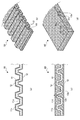
- FIG. (A) is a schematic sectional drawing explaining the cross-sectional shape of the fuse element 10 to which this invention is applied
- (b) is a perspective view of the fuse element 10.
- FIG. (C) is a schematic sectional drawing explaining the cross-sectional shape of the fuse element 20 to which this invention is applied
- (d) is a perspective view of the fuse element 20.
- FIG. (A) is a schematic sectional drawing explaining the cross-sectional shape of the fuse element 30 to which this invention is applied
- (b) is a perspective view of the fuse element 30.
- FIG. (C) is a schematic sectional drawing explaining the cross-sectional shape of the fuse element 40 to which this invention is applied
- (d) is a perspective view of the fuse element 40.
- FIG. (A) is a schematic sectional drawing explaining the cross-sectional shape of the fuse element 50 to which this invention is applied
- (b) is a perspective view of the fuse element 50
- FIG. (C) is a schematic sectional drawing explaining the cross-sectional shape of the fuse element 60 to which this invention is applied
- (d) is a perspective view of the fuse element 70
- FIG. (A) is a schematic sectional drawing explaining the cross-sectional shape of the fuse element 70 to which this invention is applied
- (b) is a perspective view of the fuse element 70.
- FIG. It is a schematic diagram explaining the application example of the fuse element to which this invention is applied. It is a schematic diagram explaining the application example of the fuse element to which this invention is applied.
- a fuse element according to an aspect of the present invention has a low melting point metal layer and a high melting point metal layer laminated on the low melting point metal layer, and the melted low melting point metal erodes and melts the high melting point metal layer.
- FIG. 1A is a schematic cross-sectional view illustrating a cross-sectional shape of a fuse element 10 to which the present invention is applied
- FIG. 1B is a perspective view of the fuse element 10.
- the fuse element 10 is a laminated structure including an inner layer and an outer layer, and includes a low melting point metal layer 11 as an inner layer and a refractory metal layer 12 as an outer layer laminated on both surfaces of the low melting point metal layer 11.
- the fuse element 10 includes a low-melting-point metal layer 11 having a high-thickness portion 11a and a low-thickness portion 11b whose thickness in the thickness direction is smaller than that of the high-thickness portion 11a.
- the low melting point metal layer 11 of the fuse element 10 has a substantially trapezoidal shape on both sides in the thickness direction of the low film thickness portion 11b formed in a substantially rectangular shape in cross section.
- the low-thickness portion 11b and the high-thickness portion 11a are continuously formed in the length direction.
- the high film thickness portion 11a is preferably configured to have a thickness that is twice or more that of the low film thickness portion 11b.
- the thickness direction represents the vertical direction of the fuse element on the paper surface of FIG. 1A
- the length direction represents the left-right direction of the fuse element on the paper surface of FIG.
- the refractory metal layer 12 of the fuse element 10 is laminated so as to have a predetermined thickness according to the outer surface shape of the low melting point metal layer 11.
- FIG. 1C is a schematic cross-sectional view illustrating a cross-sectional shape of the fuse element 20 to which the present invention is applied
- FIG. 1D is a perspective view of the fuse element 20.
- the fuse element 20 is a laminated structure including an inner layer and an outer layer, and includes a low melting point metal layer 11 as an inner layer and a refractory metal layer 12 as an outer layer laminated on the low melting point metal layer 11.
- a low melting point metal layer 11 as an inner layer and a high melting point metal layer 12 as an outer layer include a high film thickness portion 11a, a low film thickness portion 11b, a high film thickness portion 12a, and a low film thickness portion 12b, respectively. .
- the fuse element 20 includes a low melting point metal layer 11 having the same shape as the fuse element 10, and the outer shape of the fuse element 20 after the high melting point metal layer 12 is laminated.
- the refractory metal layer 12 is laminated so as to have a planar shape.
- the refractory metal layer 12 of the fuse element 20 has a high film thickness portion 12 a in the thickness direction at a portion corresponding to the low film thickness portion 11 b of the low melting metal layer 11.
- the portions corresponding to the thick portions 11a are laminated so as to have a low film thickness portion 12b having a thickness smaller than that of the high film thickness portion 12a in the thickness direction.
- FIG. 2A is a schematic cross-sectional view illustrating the cross-sectional shape of the fuse element 30 to which the present invention is applied
- FIG. 2B is a perspective view of the fuse element 30.
- FIG. The fuse element 30 is a laminated structure including an inner layer and an outer layer, and includes a low melting point metal layer 11 as an inner layer and a refractory metal layer 12 as an outer layer laminated on the low melting point metal layer 11.
- the fuse element 30 includes a low-melting-point metal layer 11 as an inner layer and a high-thickness portion 11a and a low-thickness portion 11b whose thickness in the thickness direction is smaller than that of the high-thickness portion 11a.
- the low melting point metal layer 11 of the fuse element 30 has a substantially trapezoidal shape on one side in the thickness direction of the low film thickness portion 11b formed in a substantially rectangular shape in cross section.
- the low-thickness portion 11b and the high-thickness portion 11a are continuously formed in the length direction.
- the refractory metal layer 12 of the fuse element 30 is laminated so as to have a predetermined thickness according to the outer surface shape of the low melting point metal layer 11.
- FIG. 2 (c) is a schematic cross-sectional view for explaining the cross-sectional shape of the fuse element 40 to which the present invention is applied
- FIG. 2 (d) is a perspective view of the fuse element 40.
- the fuse element 40 is a laminated structure including an inner layer and an outer layer, and includes a low melting point metal layer 11 as an inner layer and a refractory metal layer 12 as an outer layer laminated on the low melting point metal layer 11.
- the low melting point metal layer 11 as an inner layer and the high melting point metal layer 12 as an outer layer include a high film thickness portion 11a, a low film thickness portion 11b, a high film thickness portion 12a, and a low film thickness portion 12b, respectively. .
- the fuse element 40 includes a low melting point metal layer 11 having the same shape as the fuse element 30, and the outer shape of the fuse element 40 after the high melting point metal layer 12 is laminated.
- the refractory metal layer 12 is laminated so as to have a planar shape.
- the refractory metal layer 12 of the fuse element 40 has a high film thickness portion 12 a in the thickness direction at a portion corresponding to the low film thickness portion 11 b of the low melting metal layer 11.
- the portions corresponding to the thick portions 11a are laminated so as to have a low film thickness portion 12b having a thickness smaller than that of the high film thickness portion 12a in the thickness direction.
- the fuse element according to another aspect of the present invention has a low melting point metal layer and a high melting point metal layer laminated on the low melting point metal layer, and the melted low melting point metal erodes the high melting point metal layer.
- a fuse element that uses an action of fusing, and the low melting point metal layer has a mountain fold and a valley fold in the thickness direction, so that the low melting point metal layer melted at a temperature during reflow mounting is transferred. This is a limitation.
- FIG. 3A is a schematic cross-sectional view illustrating a cross-sectional shape of the fuse element 50 to which the present invention is applied
- FIG. 3B is a perspective view of the fuse element 50.
- the fuse element 50 is a laminated structure including an inner layer and an outer layer, and includes a low melting point metal layer 11 as an inner layer and a refractory metal layer 12 as an outer layer laminated on the low melting point metal layer 11.
- the low melting point metal layer 11 as an inner layer includes a mountain fold portion 11c and a valley fold portion 11d in the thickness direction.
- the low melting point metal layer 11 of the fuse element 50 has a mountain fold portion 11c and a valley fold portion 11d in a cross-sectional shape, and the mountain fold portion 11c and the valley fold.
- the folded portion 11d is formed continuously in the length direction.
- the refractory metal layer 12 of the fuse element 50 is laminated so as to have a predetermined thickness according to the outer surface shape of the low melting point metal layer 11 (the shape of the mountain fold portion 11c and the valley fold portion 11d).
- FIG. 3C is a schematic cross-sectional view illustrating the cross-sectional shape of the fuse element 60 to which the present invention is applied
- FIG. 3D is a perspective view of the fuse element 60.
- the fuse element 60 is a laminated structure including an inner layer and an outer layer, and includes a low melting point metal layer 11 as an inner layer and a refractory metal layer 12 as an outer layer laminated on the low melting point metal layer 11.
- the low melting point metal layer 11 as an inner layer includes a mountain fold part 11c and a valley fold part 11d
- the high melting point metal layer 12 as an outer layer includes a high film thickness part 12a and a low film thickness part 12b.
- the fuse element 60 includes the low melting point metal layer 11 having the same shape as the fuse element 50, and the outer shape of the fuse element 60 after the high melting point metal layer 12 is laminated.
- the refractory metal layer 12 is laminated so as to have a planar shape.
- the refractory metal layer 12 of the fuse element 60 has a low film thickness portion 12b in the thickness direction at a portion corresponding to the mountain fold portion 11c of the low melting point metal layer 11, and the valley fold portion of the low melting point metal layer 11
- the layers corresponding to 11d are laminated so as to have a high-thickness portion 12a that is thicker than the low-thickness portion 12b in the thickness direction.
- the low melting point metal layer 11 as an inner layer includes a high film thickness portion 11a and a low film thickness portion 11b whose thickness in the thickness direction is smaller than that of the high film thickness portion 11a.
- the present invention is not limited to this, and only the refractory metal layer 12 that is the outer layer may be configured to include the high-thickness portion 12a and the low-thickness portion 12b.
- FIG. 4A is a schematic cross-sectional view illustrating the cross-sectional shape of the fuse element 70 in which only the refractory metal layer 12 includes the high-thickness portion 12a and the low-thickness portion 12b, and FIG. FIG.
- the fuse element 70 is a laminated structure including an inner layer and an outer layer, and includes a low melting point metal layer 11 as an inner layer and a refractory metal layer 12 as an outer layer laminated on the low melting point metal layer 11.
- the fuse element 70 includes a high-melting point metal layer 12 as an outer layer and a high-thickness portion 12a and a low-thickness portion 12b whose thickness in the thickness direction is smaller than that of the high-thickness portion 12a.
- the low-melting point metal layer 11 of the fuse element 70 is formed in a substantially rectangular shape in cross-sectional shape, and both sides in the thickness direction are formed on the surface of the low-melting point metal layer 11.
- a refractory metal layer 12 having a high film thickness portion 12a formed in a substantially trapezoidal shape and a low film thickness portion 12b whose thickness in the thickness direction is smaller than that of the high film thickness portion 12a is laminated.
- the low melting point metal layer 11 and the high melting point metal layer 12 constituting the fuse elements 10 to 70 will be described.
- a metal material called “Pb-free solder” such as Sn, Sn—Cu alloy, Sn—Bi alloy, or Sn—Ag alloy can be used.
- Pb-free solder such as Sn, Sn—Cu alloy, Sn—Bi alloy, or Sn—Ag alloy.
- metal materials (elementary wires, foils, sheet plates) having a desired cross-sectional area can be obtained.
- the melting point of the low melting point metal layer 11 is not necessarily higher than the temperature of the reflow furnace, and may be melted at about 200 ° C. to 240 ° C.
- the high melting point metal layer 12 is a metal layer laminated on the surface of the low melting point metal layer 11, and for example, Ag, Cu, Ag, or an alloy containing Cu as a main component can be used, and the fuse elements 10 to 70 are used. In the case of mounting on an insulating substrate by a reflow furnace, it has a high melting point that does not melt.
- the fuse elements 10 to 70 are cases where the temperature of the reflow furnace exceeds the melting temperature of the low melting point metal layer 11 by laminating the high melting point metal layer 12 as the outer layer on the low melting point metal layer 11 as the inner layer. However, the fuse elements 10 to 70 do not blow out. Therefore, the fuse elements 10 to 70 can be efficiently mounted by reflow. Even if the temperature of the reflow furnace exceeds the melting temperature of the low melting point metal layer 11 and the low melting point metal is melted, either or both of the low melting point metal layer 11 and the high melting point metal layer 12 are thick. Since the high-thickness portion and the low-thickness portion having different thicknesses are provided, the movement of the low melting point metal can be suppressed.
- the fuse elements 10 to 70 are not melted by self-heating while a predetermined rated current flows. When a current having a value higher than the rated current flows, it melts by self-heating and interrupts the current path between the electrodes. At this time, in the fuse elements 10 to 70, the melted low melting point metal layer 11 erodes the refractory metal layer 12, so that the refractory metal layer 12 is melted at a temperature lower than the melting temperature. Therefore, the fuse elements 10 to 70 can be blown in a short time by utilizing the erosion action of the high melting point metal layer 12 by the low melting point metal layer 11.
- the molten metal of the fuse elements 10 to 70 is mounted on an insulating substrate via an electrode, the molten metal is divided into right and left by the physical pulling action of the electrode.
- the current path between the electrodes can be reliably interrupted.
- the fuse elements 10 to 70 are configured by laminating the high melting point metal layer 12 on the low melting point metal layer 11 as the inner layer, the fusing temperature is significantly higher than that of a conventional chip fuse made of a high melting point metal. Can be reduced. Therefore, the fuse elements 10 to 70 can have a larger cross-sectional area and can greatly improve the rated current as compared with chip fuses of the same size. In addition, it can be made smaller and thinner than a chip fuse having the same rated current, and is excellent in quick fusing.
- the fuse elements 10 to 70 can improve the resistance to a surge (pulse resistance) in which an abnormally high voltage is instantaneously applied to the electrical system in which the fuse element is incorporated. That is, the fuse elements 10 to 70 should not be blown until, for example, a current of 100 A flows for several milliseconds. In this respect, since a large current flowing in a very short time flows on the surface of the conductor (skin effect), the fuse elements 10 to 70 are provided with a refractory metal layer such as Ag plating having a low resistance value as an outer layer. The current applied by the surge can easily flow, and fusing due to self-heating can be prevented. Therefore, the fuse elements 10 to 70 can greatly improve the surge resistance compared to the conventional solder alloy fuse.
- a surge pulse resistance
- the volume of the low melting point metal layer 11 is preferably larger than the volume of the high melting point metal 12.
- the fuse elements 10 to 60 can be effectively blown in a short time by erosion of the high melting point metal layer.
- the fuse elements 10 to 60 have a covering structure in which the inner layer is a low melting point metal layer 11 and the outer layer is a high melting point metal layer 12, and the layer thickness ratio between the low melting point metal layer 11 and the high melting point metal layer 12 is low.
- the melting point metal layer 11: the high melting point metal layer 12 may be 10: 1 to 3: 1.
- the fuse elements 10 to 60 have a layer thickness ratio of the low melting point metal layer 11: the refractory metal layer 12. As the low melting point metal becomes thicker than 3: 1, the volume of the low melting point metal layer can be made larger than the volume of the high melting point metal layer.
- the layer 12 may be eroded by the low melting point metal layer 11 melted by heat during reflow mounting.
- the fuse elements 10 to 70 have either a low-melting point metal layer 11 or a high-melting point metal layer 12 in the thickness direction, or both have a high-thickness portion and a low-thickness portion having different thicknesses. It is possible to limit the movement of the low melting point metal layer melted at the temperature at the time of mounting, and to suppress the occurrence of problems such as the fusing point being deviated from the design position or the conductor resistance of the part where the low melting point metal is lost is increased. can do. Similarly, the fuse elements 10 to 70 can be configured so that the low melting point metal layer 11 has a mountain fold portion and a valley fold portion in the thickness direction, so that the low melting point metal layer melted at the temperature during reflow mounting. Movement can be restricted.
- the fuse elements 10, 30, 50, and 70 can be manufactured by pressing after forming a high melting point metal on the surface of the low melting point metal layer 11 using a plating technique.
- the fuse elements 10, 30, 50, and 70 can be efficiently manufactured by, for example, applying an Ag plating to the surface of a long solder foil and then pressing it, and cutting it according to the size when in use. And can be used easily.
- the fuse elements 20, 40, and 60 are manufactured by pressing a metal material composed of the low melting point metal layer 11 into a predetermined shape, and then forming the surface of the low melting point metal film 11 using a plating technique. can do.
- the fuse elements 10 to 70 may be manufactured by laminating a low melting point metal foil and a high melting point metal foil.
- the fuse elements 10 to 70 can be manufactured by, for example, pressing a rolled solder foil between two rolled Cu foils or an Ag foil.
- the low melting point metal foil it is preferable to select a softer material than the high melting point metal foil.
- variation in thickness can be absorbed and a low melting metal foil and a high melting metal foil can be stuck without gap.
- the film thickness of the low melting point metal foil is reduced by pressing, it is preferable to make it thick beforehand.
- the low-melting-point metal foil protrudes from the end face of the fuse element by pressing, it is preferable to cut it off and arrange the shape.
- the fuse elements 10 to 70 can form a fuse element in which a high melting point metal layer is laminated on a low melting point metal layer by using a thin film forming technique such as vapor deposition or other well-known lamination technique.
- the fuse element 10 may be configured as a fuse element 10 ′ in which the outer peripheral portion of the low melting point metal layer 11 excluding two opposing end faces is covered with the high melting point metal layer 12.
- an antioxidant film 13 may be further formed on the surface of the outermost refractory metal layer 12.
- the fuse element 10 is formed by further coating the outermost refractory metal layer 12 with an anti-oxidation film 13, so that, for example, even when Cu plating or Cu foil is formed as the refractory metal layer 12, Cu is oxidized. Can be prevented. Therefore, the fuse element 10 can prevent a situation where the fusing time is prolonged due to oxidation of Cu, and can be blown in a short time.
- the fuse element 10 can be made of an inexpensive and easily oxidized metal such as Cu as the refractory metal layer 12 and can be formed without using an expensive metal material such as Ag.
- the antioxidant film 13 can be made of the same metal material as that of the inner low melting point metal layer 11.
- Pb-free solder whose main component is Sn can be used.
- the antioxidant film 13 can be formed by performing Sn plating on the surface of the refractory metal.
- the antioxidant film 13 can also be formed by Au plating or preflux.
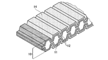
- the fuse element 10 may be provided with a protective member 14 on at least a part of the outer periphery.
- the protective member 14 prevents the inflow of connecting solder and the outflow of the low-melting metal layer 11 in the interior during reflow mounting of the fuse element 10 and maintains its shape, and also melts when a current exceeding the rated current flows. This prevents solder from flowing in and prevents the rapid fusing property from being lowered due to an increase in rated current.
- the fuse element 10 is provided with the protective member 14 on the outer periphery, so that the low melting point metal layer 11 melted at the reflow temperature can be prevented from flowing out and the element shape can be maintained.
- the protective member 14 is provided on the outer peripheral portion to provide the protection element 14 from the side surface. The low melting point metal is prevented from flowing out and the shape can be maintained.
- the fuse element 10 can prevent inflow of molten solder when a current exceeding the rated current flows by providing a protective member on the outer periphery.
- a protective member on the outer periphery to prevent the inflow of molten metal, to fix the resistance value, to quickly melt at a predetermined current value, and to provide insulation reliability between the electrodes. Can be secured.
- the protective member 14 it is preferable to use a material having insulation properties, heat resistance at a reflow temperature, and resist properties against molten solder or the like.
- the insulating resin include polyimide, polypropylene, polyvinyl chloride, polyvinylidene chloride, polytetrafluoroethylene, polystyrene, styrene-acrylonitrile copolymer, styrene-methyl methacrylate copolymer, polymethyl methacrylate. , Cellulose acetate, polyamide, phenol resin, melamine resin, silicone resin, unsaturated polyester, and the like. These insulating resins may be used alone or in combination.
- a polyimide film is used as a protective member, and the fuse element 10 having the protective member can be formed by adhering to the central portion of the tape-shaped fuse element 10 with an adhesive.
- the protective member can be formed by applying an ink having insulating properties, heat resistance, and resist properties to the outer periphery of the fuse element.
- the protective member can be formed by applying a solder resist to the outer periphery of the fuse element.
- the protective member made of the above-mentioned film, ink, solder resist, etc. can be formed by sticking or coating the outer periphery of the long fuse element, and the fuse element provided with the protective member should be cut off during use. And it is easy to handle.
- a protective case 17 that houses the fuse element 10 as shown in FIG. 8 may be used as a protective member.
- the protective case 17 includes, for example, a housing 16 whose upper surface is opened and a lid 15 that covers the upper surface of the housing.
- the protective case 17 has an opening that leads both ends of the fuse element connected to the electrode outward.
- the protective case 17 is closed except for the opening through which the fuse element is led out, and prevents intrusion of molten solder or the like into the housing.
- the protective case 17 can be formed using an engineering plastic having insulating properties, heat resistance, and resist properties.
- the protective case 17 is formed by housing the fuse element 10 from the opened upper surface side of the housing 16 as shown in FIG. 8 (b) and closing it with a lid 15 as shown in FIG. 8 (c).
- the fuse element 10 is led out from the side surface of the housing 16 by bending both ends connected to the electrodes downward.
- an opening from which the fuse element 10 is led out is formed by the convex portion formed on the inner surface of the lid 15 and the side surface of the housing 16.
- Such a fuse element provided with the protective member 14 and the protective case 17 is used by being directly mounted on a circuit board of an electronic component as it is as a fuse element in addition to being used by being incorporated in a fuse element. Good.
- FIG. 9 is a schematic sectional view for explaining the sectional shape of the fuse element 100.
- the fuse element 100 includes an insulating substrate 101, a first electrode 102 and a second electrode 103 provided on the insulating substrate 101, and between the first electrode 102 and the second electrode 103.
- a fuse element 10 that melts by self-heating when a current exceeding the rated current flows and interrupts a current path between the first electrode 102 and the second electrode 103. Covered with a cover member 107.
- the fuse element 10 is applied as a representative example of the fuse elements 10 to 70 will be described.
- other fuse elements 20 to 70 can be applied to the fuse element according to the present invention. Of course.
- the insulating substrate 101 is formed in a rectangular shape by an insulating member such as alumina, glass ceramics, mullite, zirconia.
- an insulating member such as alumina, glass ceramics, mullite, zirconia.
- a material used for a so-called printed wiring board such as a glass epoxy board or a phenol board may be used.
- the first electrode 102 and the second electrode 103 are formed on opposite ends of the insulating substrate 101.
- the first electrode 102 and the second electrode 103 are each formed by a conductive pattern such as a Cu wiring, and a protective layer 104 such as Sn plating is appropriately provided on the surface as an anti-oxidation measure.
- the first electrode 102 and the second electrode 103 extend from the front surface 101a of the insulating substrate 101 to the back surface 101b through the side surfaces.
- the fuse element 100 is mounted on the current circuit of the circuit board via the first electrode 102 and the second electrode 103 formed on the back surface 101 b of the insulating substrate 101.
- the fuse element 10 mounted between the first electrode 102 and the second electrode 103 is melted by self-heating when a current exceeding the rated current flows, and the first electrode The current path between 102 and the second electrode 103 is cut off.
- the low melting point metal layer 11 of the fuse element 10 is substantially on both sides in the thickness direction of the low film thickness portion 11b formed in a substantially rectangular shape in cross section. It has the high film thickness part 11a formed in the shape, and the low film thickness part 11b and the high film thickness part 11a are formed continuously in the length direction.
- the refractory metal layer 12 is laminated to have a predetermined thickness according to the outer surface shape of the low melting point metal layer 11.
- the fuse element 10 having such a configuration is mounted on the first electrode 102 and the second electrode 103 via an adhesive material 105 such as solder and then connected to the insulating substrate 101 by reflow soldering or the like. .
- an adhesive material 105 such as solder
- the low melting point metal layer 11 of the fuse element 10 includes a high film thickness portion and a low film thickness portion having different thicknesses, the movement of the low melting point metal layer melted at the temperature during reflow mounting is limited. In other words, it is possible to suppress the occurrence of a problem such that the melted portion is deviated from the design position or the conductor resistance of the portion where the low melting point metal is lost is increased.
- the fuse element 10 is formed separately from the insulating substrate 101 and mounted separately from the surface 101 a of the insulating substrate 101. Therefore, the fuse element 100 is drawn into the first electrode 102 and the second electrode 103 without the molten metal biting into the insulating substrate 101 even when the fuse element 10 is melted, and the first electrode 102 is surely inserted. And the second electrode 103 can be insulated.
- the flux 106 may be applied to substantially the entire outer layer on the fuse element 10.
- the flux 106 By applying the flux 106, the wettability of the low melting point metal layer 11 can be improved, and the oxide while the low melting point metal is melted can be removed to promote the erosion action on the high melting point metal.
- the flux 106 is formed on the surface of the outermost refractory metal layer 12 with an antioxidant film such as Pb-free solder containing Sn as a main component, the oxide of the antioxidant film is removed. Therefore, the refractory metal layer 12 can be prevented from being oxidized.
- the fuse element 110 may be configured such that the fuse element 10 is mounted by a clamp terminal 108 connected to the first electrode 102 and the second electrode 103 as shown in FIG. .
- the clamp terminal 108 can be easily connected by clamping the end of the fuse element 10 by pressure bonding.
- the fuse element 10 that is physically fitted and connected by the clamp terminal 108 is not only incorporated in the fuse element 100 and the fuse element 110 as shown in FIGS. 9 and 10, but, for example, as shown in FIG.
- the fuse element may be directly incorporated into a fuse box or a breaker device as it is.
- the fuse element 10 is sandwiched between the first electric wire terminal 112 and the second electric wire terminal 113 arranged on the insulating terminal block 111 and the clamp terminal 108, and the clamp terminal 108, the electric wire terminals 112, 113, and
- the bolt 114 that penetrates the insulated terminal block 111 and a fastener such as a nut 115 disposed on the back surface of the insulated terminal block 111 are fixed.
- FIG. 12A is a schematic cross-sectional view for explaining the cross-sectional shape of the fuse element 200 in which the high-melting point metal layer 12 is laminated on both surfaces of the low-melting point metal layer 11 used as a reference example in this test, and FIG. Corresponds to the fuse element 10 shown in FIG. 1 (a) as a representative example of the fuse element according to the present invention.
- the low melting point metal layer 11 has one high film thickness portion 11a and two low film thickness portions 11b. It is a schematic sectional drawing explaining the cross-sectional shape of the fuse element 300 which has this.
- Each of the fuse element 200 shown in FIG. 12A and the fuse element 300 shown in FIG. 12B is heated at 240 ° C., which is a general set temperature during reflow mounting, for 4 minutes, and then has a low melting point according to an X-ray image. The presence or absence of metal movement was confirmed.
- the fuse element 200 in which the high melting point metal layer 12 is simply laminated on both sides of the low melting point metal layer 11 the low melting point metal is thinned with heating for 4 minutes, and the uncontrollable movement of the low melting point metal is caused. Has been confirmed to occur.
- the fuse element 300 in which the low melting point metal layer 11 has one high film thickness portion 11a and two low film thickness portions 11b the movement of the low melting point metal is low even after heating for 4 minutes. It was confirmed that it was possible to control the movement of the low-melting point metal by blocking in the part 11b.
- the fuse element and the fuse element according to the present invention even if the low melting point metal melts at the temperature during reflow mounting, the fusing point is shifted from the design position or the low melting point metal is lost. It is possible to provide a fuse element and a fuse element that can suppress the occurrence of a problem such that the conductor resistance of the portion increases.
Landscapes
- Fuses (AREA)
Abstract
【課題】 リフロー実装時における温度で低融点金属が溶融したとしても、溶断箇所が設計上の位置からずれる、又は低融点金属が無くなった部分の導体抵抗が上昇するといった不具合の発生を抑制することが可能なヒューズエレメント及びヒューズ素子を提供することを目的とする。 【解決手段】 ヒューズ素子の通電経路を構成し、定格を超える電流が通電することによって自己発熱により溶断するヒューズエレメントにおいて、低融点金属層と低融点金属層に積層された高融点金属層とを有し、低融点金属層が、高融点金属層を侵食し溶断する作用を用いたヒューズエレメントであって、低融点金属層と高融点金属層との何れか又は両方が、厚さの異なる高膜厚部と低膜厚部とを有することを特徴としたヒューズエレメント及び当該ヒューズエレメントを用いたヒューズ素子。
Description
本発明は、電流経路上に実装され、定格を超える異常な電流(過電流)が流れたときに自己発熱により溶断し当該電流経路を遮断するヒューズエレメント及びヒューズ素子に関するものである。
従来から、電流経路に過電流が流れた際、当該電流経路上に配置された回路素子を保護するために、ヒューズエレメントが用いられている。このようなヒューズエレメントとしては、Pb含有ハンダが好まれて用いられている。しかしながら、2007年に施行されたRoHS指令により鉛含有ハンダの使用は制限されることとなり、今後鉛フリー化に対する要求はますます強くなるものと予想される。
このような状況下において、例えば、特許文献1には、低融点金属層の表面に高融点金属層を積層し、過電流による発熱時には、低融点金属層が溶融しながら高融点金属層を侵食することで高融点金属の融点よりも低い温度で速やかに溶断することが可能なPbフリーのヒューズエレメントについて開示がなされている。
低融点金属層の表面に高融点金属層を積層したヒューズエレメントを回路基板にリフロー実装した場合、リフロー温度で低融点金属が溶融しても積層された高融点金属は溶融しないので、エレメント形状は維持されるといった利点がある。
しかしながら、実際のリフロー条件によっては、溶融した低融点金属が高融点金属内で流動して偏在し、エレメント形状も変化してしまうことがあった。このような事象が発生した場合、溶断箇所が設計上の位置からずれる、又は低融点金属が無くなった部分の導体抵抗が上昇するといった不具合が生じる恐れがある。
本発明は、上記問題に鑑みてなされたものであり、リフロー実装時における温度で低融点金属が溶融したとしても、溶断箇所が設計上の位置からずれる、又は低融点金属が無くなった部分の導体抵抗が上昇するといった不具合の発生を抑制することが可能なヒューズエレメント及びヒューズ素子を提供することを目的とする。
上記課題を解決するために、本発明に係るヒューズエレメントは、ヒューズ素子の通電経路を構成し、定格を超える電流が通電することによって自己発熱により溶断するヒューズエレメントにおいて、低融点金属層と上記低融点金属層に積層された高融点金属層とを有し、上記低融点金属層が、上記高融点金属層を侵食し溶断する作用を用いたヒューズエレメントであって、上記低融点金属層と上記高融点金属層との何れか又は両方が、厚さの異なる高膜厚部と低膜厚部とを有することを特徴とするヒューズエレメントとしている。
また、本発明に係る他の形態のヒューズエレメントは、ヒューズ素子の通電経路を構成し、定格を超える電流が通電することによって自己発熱により溶断するヒューズエレメントにおいて、低融点金属層と上記低融点金属層に積層された高融点金属層とを有し、上記低融点金属層が、上記高融点金属層を侵食し溶断する作用を用いたヒューズエレメントであって、上記低融点金属層が、厚さ方向において山折り部と谷折り部とを有することを特徴としている。
また、本発明に係るヒューズ素子は、絶縁基板と、上記絶縁基板に搭載され、定格を超える電流が通電することによって自己発熱により溶断するヒューズエレメントとを備え、上記ヒューズエレメントは、低融点金属層と、上記低融点金属層に積層された高融点金属層とを有し、上記低融点金属層が、上記高融点金属層を侵食し溶断する作用を用いたヒューズエレメントであって、上記低融点金属層と上記高融点金属層との何れか又は両方が、厚さの異なる高膜厚部と低膜厚部とを有することを特徴としている。
本発明によれば、リフロー実装時における温度で溶融した低融点金属層の移動が制限されるため、溶断箇所が設計上の位置からずれる、又は低融点金属が無くなった部分の導体抵抗が上昇するといった不具合の発生を抑制することが可能なヒューズエレメント及びヒューズ素子を提供することができる。
以下、本発明を実施するための形態について図面を参照して説明する。なお、本発明は、以下の記述のみに限定されるものではなく、本発明の要旨を逸脱しない範囲において適宜変更可能である。また、図面は模式的なものであり、各寸法の比率等は現実のものとは異なることがある。具体的な寸法等は以下の説明を参酌して判断すべきものである。また、図面相互間においても互いの寸法の関係や比率が異なる部分が含まれていることは勿論である。
本発明の一形態に係るヒューズエレメントは、低融点金属層と当該低融点金属層に積層された高融点金属層とを有し、溶融した低融点金属が高融点金属層を侵食し溶断する作用を用いたヒューズエレメントであって、低融点金属層と高融点金属層との何れかが又は両方が厚さの異なる高膜厚部と低膜厚部とを有することで、リフロー実装時における温度で溶融した低融点金属層の移動を制限するものである。
[ヒューズエレメント]
図1(a)は本発明を適用したヒューズエレメント10の断面形状を説明する概略断面図であり、図1(b)はヒューズエレメント10の斜視図である。ヒューズエレメント10は、内層と外層とからなる積層構造体であり、内層として低融点金属層11、当該低融点金属層11の両面に積層された外層として高融点金属層12を有する。ヒューズエレメント10は、低融点金属層11が高膜厚部11aと当該高膜厚部11aよりも厚み方向における膜厚が薄い低膜厚部11bとを備える。
図1(a)は本発明を適用したヒューズエレメント10の断面形状を説明する概略断面図であり、図1(b)はヒューズエレメント10の斜視図である。ヒューズエレメント10は、内層と外層とからなる積層構造体であり、内層として低融点金属層11、当該低融点金属層11の両面に積層された外層として高融点金属層12を有する。ヒューズエレメント10は、低融点金属層11が高膜厚部11aと当該高膜厚部11aよりも厚み方向における膜厚が薄い低膜厚部11bとを備える。
図1(a)及び図1(b)に示すように、ヒューズエレメント10の低融点金属層11は、断面形状において略矩形状に形成された低膜厚部11bの厚み方向両側に略台形状に形成された高膜厚部11aを有し、低膜厚部11bと高膜厚部11aとは長さ方向において連続して形成されている。ここで、高膜厚部11aは低膜厚部11bに対して2倍以上の厚みを有するように構成するのが好ましい。なお、本発明の説明において、厚み方向とは図1(a)紙面上におけるヒューズエレメントの上下方向を表し、長さ方向とは同図紙面上においてヒューズエレメントの左右方向を表すものとする。そして、ヒューズエレメント10の高融点金属層12は、低融点金属層11の外面形状に応じて所定の厚みを有するよう積層されている。
図1(c)は本発明を適用したヒューズエレメント20の断面形状を説明する概略断面図であり、図1(d)はヒューズエレメント20の斜視図である。ヒューズエレメント20は、ヒューズエレメント10と同様に内層と外層とからなる積層構造体であり、内層として低融点金属層11、当該低融点金属層11に積層された外層として高融点金属層12を有する。ヒューズエレメント20は、内層たる低融点金属層11と外層たる高融点金属層12とが、それぞれ高膜厚部11a及び低膜厚部11bと高膜厚部12a及び低膜厚部12bとを備える。
図1(c)及び図1(d)に示すように、ヒューズエレメント20は、ヒューズエレメント10と同形状の低融点金属層11を備え、高融点金属層12積層後のヒューズエレメント20の外面形状が平面形状となるように当該高融点金属層12が積層されている。換言すると、ヒューズエレメント20の高融点金属層12は、低融点金属層11の低膜厚部11bに対応する部分において厚み方向に高膜厚部12aを有し、低融点金属層11の高膜厚部11aに対応する部分において厚み方向に高膜厚部12aよりも厚みが薄い低膜厚部12bを有するよう積層されている。
図2(a)は本発明を適用したヒューズエレメント30の断面形状を説明する概略断面図であり、図2(b)はヒューズエレメント30の斜視図である。ヒューズエレメント30は、内層と外層とからなる積層構造体であり、内層として低融点金属層11、当該低融点金属層11に積層された外層として高融点金属層12を有する。ヒューズエレメント30は、内層たる低融点金属層11が高膜厚部11aと当該高膜厚部11aよりも厚み方向における膜厚が薄い低膜厚部11bとを備える。
図2(a)及び図2(b)に示すように、ヒューズエレメント30の低融点金属層11は、断面形状において略矩形状に形成された低膜厚部11bの厚み方向片側に略台形状に形成された高膜厚部11aを有し、低膜厚部11bと高膜厚部11aとは長さ方向において連続して形成されている。そして、ヒューズエレメント30の高融点金属層12は、低融点金属層11の外面形状に応じて所定の厚みを有するよう積層されている。
図2(c)は本発明を適用したヒューズエレメント40の断面形状を説明する概略断面図であり、図2(d)はヒューズエレメント40の斜視図である。ヒューズエレメント40は、ヒューズエレメント30と同様に内層と外層とからなる積層構造体であり、内層として低融点金属層11、当該低融点金属層11に積層された外層として高融点金属層12を有する。ヒューズエレメント40は、内層たる低融点金属層11と外層たる高融点金属層12とが、それぞれ高膜厚部11a及び低膜厚部11bと高膜厚部12a及び低膜厚部12bとを備える。
図2(c)及び図2(d)に示すように、ヒューズエレメント40は、ヒューズエレメント30と同形状の低融点金属層11を備え、高融点金属層12積層後のヒューズエレメント40の外面形状が平面形状となるように当該高融点金属層12が積層されている。換言すると、ヒューズエレメント40の高融点金属層12は、低融点金属層11の低膜厚部11bに対応する部分において厚み方向に高膜厚部12aを有し、低融点金属層11の高膜厚部11aに対応する部分において厚み方向に高膜厚部12aよりも厚みが薄い低膜厚部12bを有するよう積層されている。
ここで、本発明の他の形態に係るヒューズエレメントは、低融点金属層と当該低融点金属層に積層された高融点金属層とを有し、溶融した低融点金属が高融点金属層を侵食し溶断する作用を用いたヒューズエレメントであって、低融点金属層が、厚さ方向において山折り部と谷折り部とを有することで、リフロー実装時における温度で溶融した低融点金属層の移動を制限するものである。
図3(a)は本発明を適用したヒューズエレメント50の断面形状を説明する概略断面図であり、図3(b)はヒューズエレメント50の斜視図である。ヒューズエレメント50は、内層と外層とからなる積層構造体であり、内層として低融点金属層11、当該低融点金属層11に積層された外層として高融点金属層12を有する。ヒューズエレメント50は、内層たる低融点金属層11が、厚さ方向において山折り部11cと谷折り部11dとを備える。
図3(a)及び図3(b)に示すように、ヒューズエレメント50の低融点金属層11は、断面形状において山折り部11cと谷折り部11dとを有し、山折り部11cと谷折り部11dとは長さ方向において連続して形成されている。そして、ヒューズエレメント50の高融点金属層12は、低融点金属層11の外面形状(山折り部11cと谷折り部11dとの形状)に応じて所定の厚みを有するよう積層されている。
図3(c)は本発明を適用したヒューズエレメント60の断面形状を説明する概略断面図であり、図3(d)はヒューズエレメント60の斜視図である。ヒューズエレメント60は、ヒューズエレメント50と同様に内層と外層とからなる積層構造体であり、内層として低融点金属層11、当該低融点金属層11に積層された外層として高融点金属層12を有する。ヒューズエレメント70は、内層たる低融点金属層11が山折り部11c及び谷折り部11dを、外層たる高融点金属層12が高膜厚部12a及び低膜厚部12bを備える。
図3(c)及び図3(d)に示すように、ヒューズエレメント60は、ヒューズエレメント50と同形状の低融点金属層11を備え、高融点金属層12積層後のヒューズエレメント60の外面形状が平面形状となるように当該高融点金属層12が積層されている。換言すると、ヒューズエレメント60の高融点金属層12は、低融点金属層11の山折り部11cに対応する部分において厚み方向に低膜厚部12bを有し、低融点金属層11の谷折り部11dに対応する部分において厚み方向に低膜厚部12bよりも厚みが厚い高膜厚部12aを有するよう積層されている。
ところで、ヒューズエレメント10~60等においては、内層たる低融点金属層11が高膜厚部11aと当該高膜厚部11aよりも厚み方向における膜厚が薄い低膜厚部11bとを備える構成について説明したが、これに限らず、ヒューズエレメントの構成として外層たる高融点金属層12のみが高膜厚部12a及び低膜厚部12bを備える構成とすることも可能である。
図4(a)は高融点金属層12のみが高膜厚部12a及び低膜厚部12bを備えるヒューズエレメント70の断面形状を説明する概略断面図であり、図4(b)はヒューズエレメント70の斜視図である。ヒューズエレメント70は、内層と外層とからなる積層構造体であり、内層として低融点金属層11、低融点金属層11に積層された外層として高融点金属層12を有する。ヒューズエレメント70は、外層たる高融点金属層12が高膜厚部12aと当該高膜厚部12aよりも厚み方向における膜厚が薄い低膜厚部12bとを備える。
図4(a)及び図4(b)に示すように、ヒューズエレメント70の低融点金属層11は、断面形状において略矩形状に形成されており、当該低融点金属層11表面に厚み方向両側に略台形状に形成された高膜厚部12a、当該高膜厚部12aよりも厚み方向における膜厚が薄い低膜厚部12bを有する高融点金属層12が積層されている。
次に、ヒューズエレメント10~70を構成する低融点金属層11及び高融点金属層12について説明する。低融点金属層11としては、例えば、Sn、又はSn-Cu合金、Sn-Bi合金、Sn-Ag合金といった、所謂、「Pbフリーハンダ」と称される金属材料を用いることができる。そして、これらの金属材料に対して圧延、伸線、アニール処理等を施すことにより、所望の断面積を有する金属素材(素線、箔、延板)を得ることができる。低融点金属層11の融点は、必ずしもリフロー炉の温度よりも高い必要はなく、200℃~240℃程度で溶融してもよい。また、高融点金属層12は低融点金属層11の表面に積層された金属層であり、例えば、Ag、Cu、Ag又はCuを主成分とする合金を用いることができ、ヒューズエレメント10~70をリフロー炉によって絶縁基板上に実装を行う場合においても溶融しない高い融点を有するものとする。
ヒューズエレメント10~70は、内層となる低融点金属層11に、外層として高融点金属層12を積層することによって、リフロー炉の温度が低融点金属層11の溶融温度を超えた場合であっても、ヒューズエレメント10~70として溶断するに至らない。したがって、ヒューズエレメント10~70は、リフローによって効率よく実装することができる。なお、リフロー炉の温度が低融点金属層11の溶融温度を超え、当該低融点金属が溶融したとてしても、低融点金属層11と高融点金属層12との何れか又は両方が厚さの異なる高膜厚部と低膜厚部とを有するため、低融点金属の移動を抑制することができる。
また、ヒューズエレメント10~70は、所定の定格電流が流れている間は、自己発熱によっても溶断することがない。そして、定格電流よりも高い値の電流が流れると、自己発熱によって溶融し、電極間の電流経路を遮断する。このとき、ヒューズエレメント10~70は、溶融した低融点金属層11が高融点金属層12を侵食することにより、高融点金属層12が溶融温度よりも低い温度で溶融する。したがって、ヒューズエレメント10~70は、低融点金属層11による高融点金属層12の侵食作用を利用して短時間で溶断することができる。加えて、ヒューズエレメント10~70の溶融金属は、後述するように、電極を介して絶縁基板上に実装された場合、電極の物理的な引き込み作用により左右に分断することから、速やかに、かつ確実に、電極間の電流経路を遮断することができる。
また、ヒューズエレメント10~70は、内層となる低融点金属層11に高融点金属層12が積層されて構成されているため、溶断温度を従来の高融点金属からなるチップヒューズ等よりも大幅に低減することができる。したがって、ヒューズエレメント10~70は、同一サイズのチップヒューズ等に比して、断面積を大きくでき定格電流を大幅に向上させることができる。また、同じ定格電流を持つチップヒューズよりも小型化、薄型化を図ることができ、速溶断性に優れる。
また、ヒューズエレメント10~70は、ヒューズ素子が組み込まれた電気系統に異常に高い電圧が瞬間的に印加されるサージへの耐性(耐パルス性)を向上することができる。すなわち、ヒューズエレメント10~70は、例えば、100Aの電流が数msec流れたような場合にまで溶断してはならない。この点、極短時間で流れる大電流は導体の表面を流れることから(表皮効果)、ヒューズエレメント10~70は、外層として抵抗値の低いAgメッキ等の高融点金属層が設けられているため、サージによって印加された電流を流しやすく、自己発熱による溶断を防止することができる。したがって、ヒューズエレメント10~70は、従来のハンダ合金からなるヒューズに対して、大幅にサージに対する耐性を向上させることができる。
ところで、ヒューズエレメント10~60は、低融点金属層11の体積を高融点金属12の体積よりも大きくすることが好ましい。ヒューズエレメント10~60は、低融点金属の体積を多くすることにより、効果的に高融点金属層の侵食による短時間での溶断を行うことができる。
具体的にヒューズエレメント10~60は、内層が低融点金属層11、外層が高融点金属層12の被覆構造であり、低融点金属層11と高融点金属層12との層厚比が、低融点金属層11:高融点金属層12=10:1~3:1としてもよい。これにより、確実に低融点金属層11の体積を、高融点金属層12の体積よりも多くすることができ、効果的に高融点金属層12の侵食による短時間での溶断を行うことができる。
すなわち、ヒューズエレメント10~60は、内層を構成する低融点金属層11の上下面に高融点金属層12が積層されることから、層厚比が、低融点金属層11:高融点金属層12=3:1以上に低融点金属が厚くなるほど低融点金属層の体積が高融点金属層の体積よりも多くすることができる。また、ヒューズエレメント10~60は、層厚比が、低融点金属層11:高融点金属層12=10:1を超えて低融点金属層が厚く、高融点金属層が薄くなると、高融点金属層12が、リフロー実装時の熱で溶融した低融点金属層11によって浸食されてしまう恐れがある。
そして、ヒューズエレメント10~70は、厚さ方向において低融点金属層11と高融点金属層12との何れか又は両方が厚さの異なる高膜厚部と低膜厚部とを有するため、リフロー実装時における温度で溶融した低融点金属層の移動を制限することができ、溶断箇所が設計上の位置からずれる、又は低融点金属が無くなった部分の導体抵抗が上昇するといった不具合の発生を抑制することができる。同様に、ヒューズエレメント10~70は、低融点金属層11を厚さ方向において山折り部と谷折り部とを有するよう構成することができるため、リフロー実装時における温度で溶融した低融点金属層の移動を制限することができる。
[ヒューズエレメントの製造方法]
ヒューズエレメント10、30、50、及び70は、低融点金属層11の表面に高融点金属をメッキ技術を用いて成膜後、プレス加工によて製造することができる。ヒューズエレメント10、30、50、及び70は、例えば、長尺状のハンダ箔の表面にAgメッキ等を施工後、プレス加工することによって効率よく製造でき、使用時には、サイズに応じて切断することで、容易に用いることができる。
ヒューズエレメント10、30、50、及び70は、低融点金属層11の表面に高融点金属をメッキ技術を用いて成膜後、プレス加工によて製造することができる。ヒューズエレメント10、30、50、及び70は、例えば、長尺状のハンダ箔の表面にAgメッキ等を施工後、プレス加工することによって効率よく製造でき、使用時には、サイズに応じて切断することで、容易に用いることができる。
また、ヒューズエレメント20、40、及び60は、低融点金属層11からなる金属素材を所定の形状にプレス加工後、当該低融点金属膜11の表面をメッキ技術を用いて成膜することにより製造することができる。
また、ヒューズエレメント10~70は、低融点金属箔と高融点金属箔とを貼り合わせることにより製造してもよい。ヒューズエレメント10~70は、例えば、圧延した2枚のCu箔、或はAg箔の間に、同じく圧延したハンダ箔を挟んでプレスすることにより製造することができる。この場合、低融点金属箔は、高融点金属箔よりも柔らかい材料を選択することが好ましい。これにより、厚みのばらつきを吸収して低融点金属箔と高融点金属箔とを隙間なく密着させることができる。また、低融点金属箔はプレス加工によって膜厚が薄くなるため、予め厚めにしておくとよい。プレス加工により低融点金属箔がヒューズエレメント端面よりはみ出した場合は、切り落として形を整えることが好ましい。
その他、ヒューズエレメント10~70は、蒸着等の薄膜成形技術や、他の周知の積層技術を用いることによっても、低融点金属層に高融点金属層を積層したヒューズエレメントを形成することができる。
[ヒューズエレメントの応用例]
次に、ヒューズエレメント10~70の応用例について説明する。以後の説明においては、ヒューズエレメント10~70の代表例としてヒューズエレメント10に対する応用例について説明するが、本応用例は他のヒューズエレメント20~70に適用可能であることは無論である。
次に、ヒューズエレメント10~70の応用例について説明する。以後の説明においては、ヒューズエレメント10~70の代表例としてヒューズエレメント10に対する応用例について説明するが、本応用例は他のヒューズエレメント20~70に適用可能であることは無論である。
ヒューズエレメント10は、図5に示すように、低融点金属層11の対向する2つの端面を除く外周部が高融点金属層12によって被覆されたヒューズエレメント10'として構成してもよく、図6に示すように、高融点金属層12を最外層としたときに、さらに当該最外層の高融点金属層12の表面に酸化防止膜13を形成してもよい。ヒューズエレメント10は、最外層の高融点金属層12がさらに酸化防止膜13によって被覆されることにより、例えば、高融点金属層12としてCuメッキやCu箔を形成した場合にも、Cuの酸化を防止することができる。したがって、ヒューズエレメント10は、Cuの酸化によって溶断時間が長くなる事態を防止することができ、短時間で溶断させることができる。
また、ヒューズエレメント10は、高融点金属層12としてCu等の安価で酸化しやすい金属を用いることができ、Ag等の高価な金属材料を用いることなく形成することも可能である。
また、酸化防止膜13は、内層の低融点金属層11と同じ金属材料を用いることができる。例えば、Snを主成分とするPbフリーハンダを用いることができる。また、酸化防止膜13は、高融点金属の表面にSnメッキを施すことにより形成することができる。その他、酸化防止膜13は、Auメッキやプリフラックスによっても形成することができる。
また、ヒューズエレメント10は、図7に示すように、外周の少なくとも一部に保護部材14を設けてもよい。保護部材14は、ヒューズエレメント10のリフロー実装時における接続用ハンダの流入や内装の低融点金属層11の流出を防止して形状を維持するとともに、定格電流を超える電流が流れたときにも溶融ハンダの流入を防止して定格電流の上昇による速溶断性の低下を防止するものである。
すなわち、ヒューズエレメント10は、外周に保護部材14を設けることにより、リフロー温度下で溶融した低融点金属層11の流出を防止し、エレメント形状を維持することができる。特に、低融点金属層11の上面及び下面に高融点金属層12を積層し側面から低融点金属層が露出しているヒューズエレメント10においては、外周部に保護部材14を設けることにより当該側面からの低融点金属の流出が防止され、形状を維持することができる。
また、ヒューズエレメント10は、外周に保護部材を設けることにより、定格電流を超える電流が流れたときに溶融ハンダの流入を防止することができる。ヒューズエレメント10は電極にハンダ接続されている場合、定格電流を超える電流が流れた際の発熱により、電極への接続用のハンダや低融点金属層11を構成する金属が溶融し、溶断すべきヒューズエレメント10の中央部に流入する恐れがある。ヒューズエレメント10は、ハンダ等の溶融金属が流入すると抵抗値が下がり、発熱が阻害され、所定の電流値において溶断しない、又は溶断時間が延び、或は溶断後に電極間の絶縁信頼性を損なう恐れがある。そこで、ヒューズエレメント10は、保護部材14を外周に設けることで、溶融金属の流入を防止し、抵抗値を固定させて、所定の電流値で速やかに溶断させ、かつ電極間の絶縁信頼性を確保することができる。
このため、保護部材14としては、絶縁性やリフロー温度における耐熱性を備え、かつ溶融ハンダ等に対するレジスト性を備えた材料を用いることが好ましい。絶縁性を示す樹脂しては、例えば、ポリイミド、ポリプロピレン、ポリ塩化ビニル、ポリ塩化ビニリデン、ポリテトラフルオロエチレン、ポリスチレン、スチレン-アクリロニトリル共重合体、スチレン-メタクリル酸メチル共重合体、ポリメタクリル酸メチル、酢酸セルロース、ポリアミド、フェノール樹脂、メラミン樹脂、シリコーン樹脂、不飽和ポリエステル等を挙げることができる。これらの絶縁性樹脂は単独で用いてもよく、複数組み合わせてもよい。そして、例えば、保護部材として、ポリイミドフィルムを用い、接着剤によってテープ状のヒューズエレメント10の中央部に貼り付けることにより保護部材を有するヒューズエレメント10を形成することができる。また、保護部材は、絶縁性、耐熱性、レジスト性を備えたインクをヒューズエレメントの外周に塗布することにより形成することができる。或は、保護部材は、ソルダーレジストを用い、ヒューズエレメントの外周に塗布することにより形成することができる。
上述したフィルム、インク、ソルダーレジスト等からなる保護部材は、長尺状のヒューズエレメントの外周に貼着又は塗工により形成することができ、また使用時には保護部材が設けられたヒューズエレメントを切断すればよく、取扱い性にも優れる。
また、保護部材として、図8に示すような、ヒューズエレメント10を収納する保護ケース17を用いてもよい。図8(a)に示すように、この保護ケース17は、例えば、上面が開口された筐体16と、筐体の上面を覆う蓋体15とからなる。保護ケース17は、電極と接続されるヒューズエレメントの両端を外方へ導出させる開口部を有する。保護ケース17は、ヒューズエレメントを導出する開口部を除き閉塞され、溶融ハンダ等の筐体内への侵入を防止する。保護ケース17は、絶縁性、耐熱性、レジスト性を備えたエンジニアリングプラスチック等を用いて形成することができる。
保護ケース17は、図8(b)に示すように筐体16の開口された上面側よりヒューズエレメント10を収納し、図8(c)に示すように蓋体15によって閉塞することにより形成される。ヒューズエレメント10は、電極と接続される両端が下方に折り曲げられ、筐体16の側面より導出される。筐体16は、蓋体15によって閉塞されることにより、蓋体15の内面に形成された凸部と筐体16の側面によって、ヒューズエレメント10が導出する開口部が形成される。
このような保護部材14や保護ケース17が設けられたヒューズエレメントは、ヒューズ素子に組み込まれて用いられる以外にも、自身がヒューズ素子として、そのまま電子部品の回路基板上に直接表面実装されてもよい。
[ヒューズ素子]
次に、本発明を適用したヒューズ素子100について説明する。図9はヒューズ素子100の断面形状を説明する概略断面図である。図9に示すように、ヒューズ素子100は絶縁基板101と、絶縁基板101上に設けられた第1の電極102及び第2の電極103と、第1の電極102及び第2の電極103の間に亘って実装され、定格電流を超える電流が流れた際に自己発熱によって溶断し、当該第1の電極102と第2の電極103との間の電流経路を遮断するヒューズエレメント10とを備え、カバー部材107で覆われている。なお、以後の説明においても、ヒューズエレメント10~70の代表例としてヒューズエレメント10を適用した例について説明するが、本発明に係るヒューズ素子には他のヒューズエレメント20~70が適用可能であることは無論である。
次に、本発明を適用したヒューズ素子100について説明する。図9はヒューズ素子100の断面形状を説明する概略断面図である。図9に示すように、ヒューズ素子100は絶縁基板101と、絶縁基板101上に設けられた第1の電極102及び第2の電極103と、第1の電極102及び第2の電極103の間に亘って実装され、定格電流を超える電流が流れた際に自己発熱によって溶断し、当該第1の電極102と第2の電極103との間の電流経路を遮断するヒューズエレメント10とを備え、カバー部材107で覆われている。なお、以後の説明においても、ヒューズエレメント10~70の代表例としてヒューズエレメント10を適用した例について説明するが、本発明に係るヒューズ素子には他のヒューズエレメント20~70が適用可能であることは無論である。
絶縁基板101は、例えば、アルミナ、ガラスセラミックス、ムライト、ジルコニア等の絶縁性を有する部材によって方形状に形成される。その他、絶縁基板101としては、ガラスエポキシ基板、フェノール基板等の、所謂、プリント配線用基板に用いられる材料を用いてもよい。
そして、絶縁基板101の相対向する両端部には、第1の電極102及び第2の電極103が形成されている。第1の電極102及び第2の電極103は、それぞれ、Cu配線等の導電パターンによって形成され、表面に適宜、酸化防止対策としてSnメッキ等の保護層104が設けられている。また、第1の電極102及び第2の電極103は絶縁基板101の表面101aより、側面を介して裏面101bに至る。ヒューズ素子100は、絶縁基板101の裏面101bに形成された第1の電極102及び第2の電極103を介して回路基板の電流回路上に実装される。
前述したとおり、第1の電極102及び第2の電極103との間に亘って実装されたヒューズエレメント10は、定格電流を超える電流が流れたときに、自己発熱により溶断し、第1の電極102と第2の電極103との間の電流経路を遮断するものである。図1(a)及び図1(b)で示したように、ヒューズエレメント10の低融点金属層11は、断面形状において略矩形状に形成された低膜厚部11bの厚み方向両側に略台形状に形成された高膜厚部11aを有し、低膜厚部11bと高膜厚部11aとは長さ方向において連続して形成されている。加えて、高融点金属層12は、低融点金属層11の外面形状に応じて所定の厚みを有するよう積層されている。このような構成を有するヒューズエレメント10は、ハンダ等の接着材料105を介して第1の電極102及び第2の電極103に搭載された後、リフローハンダ付け等により絶縁基板101上に接続される。このとき、ヒューズエレメント10の低融点金属層11は、厚さの異なる高膜厚部と低膜厚部とを備えるため、リフロー実装時における温度で溶融した低融点金属層の移動が制限されることとなり、溶断箇所が設計上の位置からずれる、又は低融点金属が無くなった部分の導体抵抗が上昇するといった不具合の発生を抑制することができる。
また、本発明に係るヒューズ素子100では、絶縁基板101とは別に単体でヒューズエレメント10を形成し、且つ絶縁基板101の表面101aから離間して実装されている。したがって、ヒューズ素子100は、ヒューズエレメント10の溶断時にも、溶融金属が絶縁基板101へ食い込むこともなく、第1の電極102及び第2の電極103上に引き込まれ、確実に第1の電極102と第2の電極103との間を絶縁することができる。
さらに、本発明に係るヒューズ素子100では、ヒューズエレメント10上の外層の略全面にフラックス106を塗布する形態としてもよい。フラックス106を塗布することにより、低融点金属層11の濡れ性を高めるとともに、低融点金属が溶融している間の酸化物を除去し、高融点金属への侵食作用を促進させることができる。また、フラックス106を、最外層の高融点金属層12の表面に、Snを主成分とするPbフリーハンダ等の酸化防止膜を形成した場合においても、当該酸化防止膜の酸化物を除去することができるため、高融点金属層12の酸化を防止することができる。
また、本発明の他の形態としてヒューズ素子110は、図10に示すように、ヒューズエレメント10を第1の電極102及び第2の電極103と接続されたクランプ端子108によって実装する形態としてもよい。クランプ端子108は、ヒューズエレメント10の端部を圧着により挟持することで、容易に接続することができる。
クランプ端子108によって物理的に嵌合接続するヒューズエレメント10は、図9及び図10に示すようなヒューズ素子100及びヒューズ素子110に組み込まれる以外にも、例えば、図11に示すように、自身がヒューズ素子として、そのままヒューズボックスやブレーカー装置に直接組み込む形態としてもかまわない。この場合、ヒューズエレメント10は、絶縁端子台111上に配設された第1の電線端子112及び第2の電線端子113とクランプ端子108とによって挟持され、クランプ端子108、電線端子112、113及び絶縁端子台111を貫通するボルト114と絶縁端子台111の裏面に配されたナット115等の締結具によって固定される。
[低融点金属の移動抑制効果試験]
次に、本発明を適用したヒューズエレメントでの低融点金属の移動抑制効果試験について説明する。図12(a)は本試験において参照例として用いた低融点金属層11の両面に高融点金属層12を積層したヒューズエレメント200の断面形状を説明する概略断面図であり、図12(b)は本発明に係るヒューズエレメントの代表例として図1(a)に示すヒューズエレメント10に相当し、低融点金属層11が1か所の高膜厚部11aと2ヶ所の低膜厚部11bとを有するヒューズエレメント300の断面形状を説明する概略断面図である。
次に、本発明を適用したヒューズエレメントでの低融点金属の移動抑制効果試験について説明する。図12(a)は本試験において参照例として用いた低融点金属層11の両面に高融点金属層12を積層したヒューズエレメント200の断面形状を説明する概略断面図であり、図12(b)は本発明に係るヒューズエレメントの代表例として図1(a)に示すヒューズエレメント10に相当し、低融点金属層11が1か所の高膜厚部11aと2ヶ所の低膜厚部11bとを有するヒューズエレメント300の断面形状を説明する概略断面図である。
図12(a)に示すヒューズエレメント200及び図12(b)に示すヒューズエレメント300のそれぞれをリフロー実装時の一般的な設定温度である240℃で、4分間加熱後、X線画像により低融点金属の移動有無を確認した。
その結果、単に低融点金属層11の両面に高融点金属層12を積層したヒューズエレメント200では、4分間の加熱に伴い低融点金属の厚みが薄い箇所が生じ、低融点金属の制御不能な移動が発生していることが確認された。一方、低融点金属層11が1か所の高膜厚部11aと2ヶ所の低膜厚部11bとを有するヒューズエレメント300では、4分間の加熱後においても低融点金属の移動が低膜厚部11bにおいてブロックされ、当該低融点金属の移動を制御することが可能であることが確認された。
以上のように、本発明に係るヒューズエレメント及びヒューズ素子によれば、リフロー実装時における温度で低融点金属が溶融したとしても、溶断箇所が設計上の位置からずれる、又は低融点金属が無くなった部分の導体抵抗が上昇するといった不具合の発生を抑制することが可能なヒューズエレメント及びヒューズ素子を提供することができる。
10、20、30、40、50、60、70 ヒューズエレメント
11 低融点金属層
12 低融点金属層
11a、12a 高膜厚部
11b、12b 低膜厚部
13 酸化防止膜
14 保護部材
15 蓋部
16 筐体
17 保護ケース
100、110 ヒューズ素子
101 絶縁基板
102 第1の電極
103 第2の電極
104 保護層
105 接着材料
106 フラックス
107 カバー部材
108 クランプ端子
111 結合端子台
112 第1の電線端子
113 第2の電線端子
114 ボルト
115 ナット
11 低融点金属層
12 低融点金属層
11a、12a 高膜厚部
11b、12b 低膜厚部
13 酸化防止膜
14 保護部材
15 蓋部
16 筐体
17 保護ケース
100、110 ヒューズ素子
101 絶縁基板
102 第1の電極
103 第2の電極
104 保護層
105 接着材料
106 フラックス
107 カバー部材
108 クランプ端子
111 結合端子台
112 第1の電線端子
113 第2の電線端子
114 ボルト
115 ナット
Claims (10)
- ヒューズ素子の通電経路を構成し、定格を超える電流が通電することによって自己発熱により溶断するヒューズエレメントにおいて、
低融点金属層と
上記低融点金属層に積層された高融点金属層とを有し、
上記低融点金属層が、上記高融点金属層を侵食し溶断する作用を用いたヒューズエレメントであって、
上記低融点金属層と上記高融点金属層との何れか又は両方が、厚さの異なる高膜厚部と低膜厚部とを有することを特徴とするヒューズエレメント。 - 上記低融点金属層のみが厚さの異なる高膜厚部と低膜厚部とを有することを特徴とする請求項1に記載のヒューズエレメント。
- 上記高融点金属層のみが厚さの異なる高膜厚部と低膜厚部とを有することを特徴とする請求項1に記載のヒューズエレメント。
- 上記高膜厚部と上記低膜厚部とは長さ方向において連続して形成されることを特徴とする請求項1乃至請求項3の何れか1項に記載のヒューズエレメント。
- 上記高膜厚部は上記低膜厚部に対して2倍以上の膜厚を有することを特徴とする請求項1乃至請求項4の何れか1項に記載のヒューズエレメント。
- ヒューズ素子の通電経路を構成し、定格を超える電流が通電することによって自己発熱により溶断するヒューズエレメントにおいて、
低融点金属層と
上記低融点金属層に積層された高融点金属層とを有し、
上記低融点金属層が、上記高融点金属層を侵食し溶断する作用を用いたヒューズエレメントであって、
上記低融点金属層が、厚さ方向において山折り部と谷折り部とを有することを特徴とするヒューズエレメント。 - 上記山折り部と上記谷折り部とは長さ方向において連続して形成されることを特徴とする請求項6に記載のヒューズエレメント。
- 上記低融点金属層はハンダであり、
上記高融点金属層はAg、Cu,Ag又はCuを主成分とする合金であることを特徴とする請求項1乃至請求項7の何れか1項に記載のヒューズエレメント。 - 上記低融点金属層と上記高融点金属層の層厚比は低融点金属層:高融点金属層=10:1~3:1であることを特徴とする請求項1乃至請求項8の何れか1項に記載のヒューズエレメント。
- 絶縁基板と、
上記絶縁基板に搭載され、定格を超える電流が通電することによって自己発熱により溶断するヒューズエレメントとを備え、
上記ヒューズエレメントは、
低融点金属層と、
上記低融点金属層に積層された高融点金属層とを有し、
上記低融点金属層が、上記高融点金属層を侵食し溶断する作用を用いたヒューズエレメントであって、
上記低融点金属層と上記高融点金属層との何れか又は両方が、厚さの異なる高膜厚部と低膜厚部とを有することを特徴とするヒューズ素子。
Applications Claiming Priority (2)
| Application Number | Priority Date | Filing Date | Title |
|---|---|---|---|
| JP2015-048355 | 2015-03-11 | ||
| JP2015048355A JP6714943B2 (ja) | 2015-03-11 | 2015-03-11 | ヒューズエレメント及びヒューズ素子 |
Publications (1)
| Publication Number | Publication Date |
|---|---|
| WO2016143353A1 true WO2016143353A1 (ja) | 2016-09-15 |
Family
ID=56880253
Family Applications (1)
| Application Number | Title | Priority Date | Filing Date |
|---|---|---|---|
| PCT/JP2016/001356 Ceased WO2016143353A1 (ja) | 2015-03-11 | 2016-03-10 | ヒューズエレメント及びヒューズ素子 |
Country Status (3)
| Country | Link |
|---|---|
| JP (1) | JP6714943B2 (ja) |
| TW (1) | TW201707036A (ja) |
| WO (1) | WO2016143353A1 (ja) |
Cited By (3)
| Publication number | Priority date | Publication date | Assignee | Title |
|---|---|---|---|---|
| WO2018051774A1 (ja) * | 2016-09-16 | 2018-03-22 | デクセリアルズ株式会社 | ヒューズエレメント、ヒューズ素子、保護素子 |
| CN113506716A (zh) * | 2021-08-17 | 2021-10-15 | 西安中熔电气股份有限公司 | 一种固态预制灭弧模块 |
| WO2025249521A1 (ja) * | 2024-05-31 | 2025-12-04 | デクセリアルズ株式会社 | 保護素子 |
Families Citing this family (1)
| Publication number | Priority date | Publication date | Assignee | Title |
|---|---|---|---|---|
| JP2024157602A (ja) * | 2023-04-26 | 2024-11-08 | デクセリアルズ株式会社 | 保護素子 |
Citations (5)
| Publication number | Priority date | Publication date | Assignee | Title |
|---|---|---|---|---|
| JPS56134438A (en) * | 1980-03-25 | 1981-10-21 | Mitsubishi Electric Corp | Method of producing fuse element |
| JPS57109558U (ja) * | 1980-12-25 | 1982-07-06 | ||
| JP2009099372A (ja) * | 2007-10-17 | 2009-05-07 | Taiheiyo Seiko Kk | ヒューズエレメント及びこのヒューズエレメントを用いてなるヒュージブルリンク |
| WO2015025883A1 (ja) * | 2013-08-21 | 2015-02-26 | デクセリアルズ株式会社 | 保護素子 |
| WO2015030023A1 (ja) * | 2013-08-28 | 2015-03-05 | デクセリアルズ株式会社 | ヒューズエレメント、ヒューズ素子 |
-
2015
- 2015-03-11 JP JP2015048355A patent/JP6714943B2/ja active Active
-
2016
- 2016-03-08 TW TW105107061A patent/TW201707036A/zh unknown
- 2016-03-10 WO PCT/JP2016/001356 patent/WO2016143353A1/ja not_active Ceased
Patent Citations (5)
| Publication number | Priority date | Publication date | Assignee | Title |
|---|---|---|---|---|
| JPS56134438A (en) * | 1980-03-25 | 1981-10-21 | Mitsubishi Electric Corp | Method of producing fuse element |
| JPS57109558U (ja) * | 1980-12-25 | 1982-07-06 | ||
| JP2009099372A (ja) * | 2007-10-17 | 2009-05-07 | Taiheiyo Seiko Kk | ヒューズエレメント及びこのヒューズエレメントを用いてなるヒュージブルリンク |
| WO2015025883A1 (ja) * | 2013-08-21 | 2015-02-26 | デクセリアルズ株式会社 | 保護素子 |
| WO2015030023A1 (ja) * | 2013-08-28 | 2015-03-05 | デクセリアルズ株式会社 | ヒューズエレメント、ヒューズ素子 |
Cited By (5)
| Publication number | Priority date | Publication date | Assignee | Title |
|---|---|---|---|---|
| WO2018051774A1 (ja) * | 2016-09-16 | 2018-03-22 | デクセリアルズ株式会社 | ヒューズエレメント、ヒューズ素子、保護素子 |
| JP2018045979A (ja) * | 2016-09-16 | 2018-03-22 | デクセリアルズ株式会社 | ヒューズエレメント、ヒューズ素子、保護素子 |
| US10410818B2 (en) | 2016-09-16 | 2019-09-10 | Dexerials Corporation | Fuse element, fuse device, and protective device |
| CN113506716A (zh) * | 2021-08-17 | 2021-10-15 | 西安中熔电气股份有限公司 | 一种固态预制灭弧模块 |
| WO2025249521A1 (ja) * | 2024-05-31 | 2025-12-04 | デクセリアルズ株式会社 | 保護素子 |
Also Published As
| Publication number | Publication date |
|---|---|
| TW201707036A (zh) | 2017-02-16 |
| JP2016170892A (ja) | 2016-09-23 |
| JP6714943B2 (ja) | 2020-07-01 |
Similar Documents
| Publication | Publication Date | Title |
|---|---|---|
| KR102213303B1 (ko) | 퓨즈 엘리먼트, 및 퓨즈 소자 | |
| JP6483987B2 (ja) | ヒューズエレメント、ヒューズ素子、及び発熱体内蔵ヒューズ素子 | |
| JP6437262B2 (ja) | 実装体の製造方法、温度ヒューズ素子の実装方法及び温度ヒューズ素子 | |
| CN105593965B (zh) | 电流熔断器 | |
| CN105518820B (zh) | 熔丝元件及熔丝单元 | |
| US10410818B2 (en) | Fuse element, fuse device, and protective device | |
| KR102442404B1 (ko) | 퓨즈 소자 | |
| TWI685872B (zh) | 熔絲元件、及熔絲單元 | |
| JP6436729B2 (ja) | ヒューズエレメント、ヒューズ素子、保護素子、短絡素子、切替素子 | |
| WO2016143353A1 (ja) | ヒューズエレメント及びヒューズ素子 | |
| WO2015083341A1 (ja) | スイッチ素子、スイッチ回路、及び警報回路 | |
| TWI731050B (zh) | 保護元件 |
Legal Events
| Date | Code | Title | Description |
|---|---|---|---|
| 121 | Ep: the epo has been informed by wipo that ep was designated in this application |
Ref document number: 16761326 Country of ref document: EP Kind code of ref document: A1 |
|
| NENP | Non-entry into the national phase |
Ref country code: DE |
|
| 122 | Ep: pct application non-entry in european phase |
Ref document number: 16761326 Country of ref document: EP Kind code of ref document: A1 |