WO2016139727A1 - Semiconductor storage device and method for manufacturing same - Google Patents
Semiconductor storage device and method for manufacturing same Download PDFInfo
- Publication number
- WO2016139727A1 WO2016139727A1 PCT/JP2015/056102 JP2015056102W WO2016139727A1 WO 2016139727 A1 WO2016139727 A1 WO 2016139727A1 JP 2015056102 W JP2015056102 W JP 2015056102W WO 2016139727 A1 WO2016139727 A1 WO 2016139727A1
- Authority
- WO
- WIPO (PCT)
- Prior art keywords
- forming
- recess
- insulating
- electrode
- pillar
- Prior art date
Links
- 239000004065 semiconductor Substances 0.000 title claims abstract description 88
- 238000004519 manufacturing process Methods 0.000 title claims description 36
- 238000000034 method Methods 0.000 title claims description 36
- 239000010410 layer Substances 0.000 claims description 99
- 238000005530 etching Methods 0.000 claims description 17
- 239000011229 interlayer Substances 0.000 claims description 13
- 239000000758 substrate Substances 0.000 claims description 11
- 230000008569 process Effects 0.000 claims description 4
- 238000010030 laminating Methods 0.000 claims 2
- 238000009413 insulation Methods 0.000 abstract 9
- XUIMIQQOPSSXEZ-UHFFFAOYSA-N Silicon Chemical compound [Si] XUIMIQQOPSSXEZ-UHFFFAOYSA-N 0.000 description 64
- 229910052710 silicon Inorganic materials 0.000 description 64
- 239000010703 silicon Substances 0.000 description 64
- 230000015654 memory Effects 0.000 description 31
- VYPSYNLAJGMNEJ-UHFFFAOYSA-N Silicium dioxide Chemical compound O=[Si]=O VYPSYNLAJGMNEJ-UHFFFAOYSA-N 0.000 description 25
- 229910052814 silicon oxide Inorganic materials 0.000 description 25
- 229910000449 hafnium oxide Inorganic materials 0.000 description 24
- WIHZLLGSGQNAGK-UHFFFAOYSA-N hafnium(4+);oxygen(2-) Chemical compound [O-2].[O-2].[Hf+4] WIHZLLGSGQNAGK-UHFFFAOYSA-N 0.000 description 24
- 230000004888 barrier function Effects 0.000 description 8
- 229910052751 metal Inorganic materials 0.000 description 8
- 239000002184 metal Substances 0.000 description 8
- WFKWXMTUELFFGS-UHFFFAOYSA-N tungsten Chemical compound [W] WFKWXMTUELFFGS-UHFFFAOYSA-N 0.000 description 7
- 229910052721 tungsten Inorganic materials 0.000 description 7
- 239000010937 tungsten Substances 0.000 description 7
- 229910052581 Si3N4 Inorganic materials 0.000 description 6
- HQVNEWCFYHHQES-UHFFFAOYSA-N silicon nitride Chemical compound N12[Si]34N5[Si]62N3[Si]51N64 HQVNEWCFYHHQES-UHFFFAOYSA-N 0.000 description 6
- 238000001020 plasma etching Methods 0.000 description 5
- NBIIXXVUZAFLBC-UHFFFAOYSA-N Phosphoric acid Chemical compound OP(O)(O)=O NBIIXXVUZAFLBC-UHFFFAOYSA-N 0.000 description 4
- 239000011162 core material Substances 0.000 description 4
- 230000000694 effects Effects 0.000 description 4
- 229910021420 polycrystalline silicon Inorganic materials 0.000 description 4
- 229920005591 polysilicon Polymers 0.000 description 4
- 238000005229 chemical vapour deposition Methods 0.000 description 3
- 239000011159 matrix material Substances 0.000 description 3
- 238000001039 wet etching Methods 0.000 description 3
- 229910000147 aluminium phosphate Inorganic materials 0.000 description 2
- 230000008878 coupling Effects 0.000 description 2
- 238000010168 coupling process Methods 0.000 description 2
- 238000005859 coupling reaction Methods 0.000 description 2
- 238000000151 deposition Methods 0.000 description 2
- 230000006870 function Effects 0.000 description 2
- 239000011810 insulating material Substances 0.000 description 2
- 241000293849 Cordylanthus Species 0.000 description 1
- NRTOMJZYCJJWKI-UHFFFAOYSA-N Titanium nitride Chemical compound [Ti]#N NRTOMJZYCJJWKI-UHFFFAOYSA-N 0.000 description 1
- 230000005684 electric field Effects 0.000 description 1
- 239000012535 impurity Substances 0.000 description 1
- 230000010354 integration Effects 0.000 description 1
- 238000012986 modification Methods 0.000 description 1
- 230000004048 modification Effects 0.000 description 1
- 230000003647 oxidation Effects 0.000 description 1
- 238000007254 oxidation reaction Methods 0.000 description 1
- UAJUXJSXCLUTNU-UHFFFAOYSA-N pranlukast Chemical compound C=1C=C(OCCCCC=2C=CC=CC=2)C=CC=1C(=O)NC(C=1)=CC=C(C(C=2)=O)C=1OC=2C=1N=NNN=1 UAJUXJSXCLUTNU-UHFFFAOYSA-N 0.000 description 1
- 229960004583 pranlukast Drugs 0.000 description 1
Images


Classifications
-
- H—ELECTRICITY
- H01—ELECTRIC ELEMENTS
- H01L—SEMICONDUCTOR DEVICES NOT COVERED BY CLASS H10
- H01L29/00—Semiconductor devices adapted for rectifying, amplifying, oscillating or switching, or capacitors or resistors with at least one potential-jump barrier or surface barrier, e.g. PN junction depletion layer or carrier concentration layer; Details of semiconductor bodies or of electrodes thereof ; Multistep manufacturing processes therefor
- H01L29/40—Electrodes ; Multistep manufacturing processes therefor
- H01L29/41—Electrodes ; Multistep manufacturing processes therefor characterised by their shape, relative sizes or dispositions
- H01L29/423—Electrodes ; Multistep manufacturing processes therefor characterised by their shape, relative sizes or dispositions not carrying the current to be rectified, amplified or switched
- H01L29/42312—Gate electrodes for field effect devices
- H01L29/42316—Gate electrodes for field effect devices for field-effect transistors
- H01L29/4232—Gate electrodes for field effect devices for field-effect transistors with insulated gate
- H01L29/42324—Gate electrodes for transistors with a floating gate
-
- H—ELECTRICITY
- H01—ELECTRIC ELEMENTS
- H01L—SEMICONDUCTOR DEVICES NOT COVERED BY CLASS H10
- H01L29/00—Semiconductor devices adapted for rectifying, amplifying, oscillating or switching, or capacitors or resistors with at least one potential-jump barrier or surface barrier, e.g. PN junction depletion layer or carrier concentration layer; Details of semiconductor bodies or of electrodes thereof ; Multistep manufacturing processes therefor
- H01L29/40—Electrodes ; Multistep manufacturing processes therefor
- H01L29/401—Multistep manufacturing processes
- H01L29/4011—Multistep manufacturing processes for data storage electrodes
- H01L29/40114—Multistep manufacturing processes for data storage electrodes the electrodes comprising a conductor-insulator-conductor-insulator-semiconductor structure
-
- H—ELECTRICITY
- H01—ELECTRIC ELEMENTS
- H01L—SEMICONDUCTOR DEVICES NOT COVERED BY CLASS H10
- H01L29/00—Semiconductor devices adapted for rectifying, amplifying, oscillating or switching, or capacitors or resistors with at least one potential-jump barrier or surface barrier, e.g. PN junction depletion layer or carrier concentration layer; Details of semiconductor bodies or of electrodes thereof ; Multistep manufacturing processes therefor
- H01L29/66—Types of semiconductor device ; Multistep manufacturing processes therefor
- H01L29/68—Types of semiconductor device ; Multistep manufacturing processes therefor controllable by only the electric current supplied, or only the electric potential applied, to an electrode which does not carry the current to be rectified, amplified or switched
- H01L29/76—Unipolar devices, e.g. field effect transistors
- H01L29/772—Field effect transistors
- H01L29/78—Field effect transistors with field effect produced by an insulated gate
- H01L29/788—Field effect transistors with field effect produced by an insulated gate with floating gate
- H01L29/7881—Programmable transistors with only two possible levels of programmation
- H01L29/7883—Programmable transistors with only two possible levels of programmation charging by tunnelling of carriers, e.g. Fowler-Nordheim tunnelling
-
- H—ELECTRICITY
- H10—SEMICONDUCTOR DEVICES; ELECTRIC SOLID-STATE DEVICES NOT OTHERWISE PROVIDED FOR
- H10B—ELECTRONIC MEMORY DEVICES
- H10B41/00—Electrically erasable-and-programmable ROM [EEPROM] devices comprising floating gates
- H10B41/20—Electrically erasable-and-programmable ROM [EEPROM] devices comprising floating gates characterised by three-dimensional arrangements, e.g. with cells on different height levels
- H10B41/23—Electrically erasable-and-programmable ROM [EEPROM] devices comprising floating gates characterised by three-dimensional arrangements, e.g. with cells on different height levels with source and drain on different levels, e.g. with sloping channels
- H10B41/27—Electrically erasable-and-programmable ROM [EEPROM] devices comprising floating gates characterised by three-dimensional arrangements, e.g. with cells on different height levels with source and drain on different levels, e.g. with sloping channels the channels comprising vertical portions, e.g. U-shaped channels
-
- H—ELECTRICITY
- H10—SEMICONDUCTOR DEVICES; ELECTRIC SOLID-STATE DEVICES NOT OTHERWISE PROVIDED FOR
- H10B—ELECTRONIC MEMORY DEVICES
- H10B41/00—Electrically erasable-and-programmable ROM [EEPROM] devices comprising floating gates
- H10B41/30—Electrically erasable-and-programmable ROM [EEPROM] devices comprising floating gates characterised by the memory core region
- H10B41/35—Electrically erasable-and-programmable ROM [EEPROM] devices comprising floating gates characterised by the memory core region with a cell select transistor, e.g. NAND
Definitions
- Embodiments described herein relate generally to a semiconductor memory device and a method for manufacturing the same.
- NAND flash memories have increased the degree of integration by reducing the planar structure and reduced the bit cost, but the miniaturization of the planar structure is approaching the limit. Therefore, in recent years, a technique for stacking memory cells in the vertical direction has been proposed. However, such a stacked memory device is difficult to manufacture, and the reliability of the product after completion becomes a problem.
- An object of the embodiment is to provide a highly reliable semiconductor memory device and a manufacturing method thereof.
- the semiconductor memory device includes a pair of first electrodes, a semiconductor pillar, an inter-pillar insulating member, a first insulating film, a second electrode, and a second insulating film.
- the pair of first electrodes extend in the first direction to be spaced apart from each other.
- the semiconductor pillars and the inter-pillar insulating members are alternately arranged along the first direction between the pair of first electrodes.
- the semiconductor pillar and the inter-pillar insulating member extend in a second direction intersecting the first direction.
- the first insulating film is provided around the semiconductor pillar.
- the second electrode is provided between each of the pair of first electrodes and the first insulating film.
- the second electrode is not provided between the semiconductor pillar and the inter-pillar insulating member.
- the second insulating film is provided between the second electrode and the first electrode.
- the stacked body is formed by alternately stacking the interlayer insulating film and the first film.
- a trench extending in a first direction intersecting a stacking direction of the interlayer insulating film and the first film is formed in the stacked body.
- a plurality of inter-pillar insulating members spaced apart from each other along the first direction are formed in the trench.
- the isotropic etching is performed on the first film through the hole sandwiched between the insulating members between the pillars in the trench, so that the hole communicates with the hole between the interlayer insulating films. 1 recess is formed.
- a first insulating layer is formed on the inner surface of the first recess, and a second electrode is formed in the first recess.
- a first insulating film is formed on the inner surface of the hole.
- a semiconductor pillar is formed on the first insulating film.
- slits extending in the first direction are formed in a portion between the trenches in the stacked body.
- a second recess is formed between the interlayer insulating films by removing the first film through the slit.
- the method forms a second insulating layer on the inner surface of the second recess.
- the method forms a first electrode in the second recess.
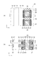
- FIG. 1A and FIG. 1B are cross-sectional views illustrating the semiconductor memory device according to the first embodiment.
- 2A and 2B are partially enlarged cross-sectional views illustrating the semiconductor memory device according to the first embodiment.
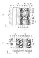
- FIG. 3 is a flowchart illustrating the method for manufacturing the semiconductor memory device according to the first embodiment.
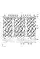
- FIG. 4A and FIG. 4B are cross-sectional views illustrating the method for manufacturing the semiconductor memory device according to the first embodiment.
- FIG. 5A and FIG. 5B are cross-sectional views illustrating the method for manufacturing the semiconductor memory device according to the first embodiment.
- 6A and 6B are cross-sectional views illustrating the method for manufacturing the semiconductor memory device according to the first embodiment.
- FIGS. 10A and 10B are cross-sectional views illustrating the method for manufacturing the semiconductor memory device according to the first embodiment.
- FIG. 11A and FIG. 11B are cross-sectional views illustrating the method for manufacturing the semiconductor memory device according to the first embodiment.
- FIG. 12A and FIG. 12B are cross-sectional views illustrating the method for manufacturing the semiconductor memory device according to the first embodiment.
- FIG. 13B are cross-sectional views illustrating the method for manufacturing the semiconductor memory device according to the first embodiment.
- FIG. 14A and FIG. 14B are cross-sectional views illustrating the method for manufacturing the semiconductor memory device according to the first embodiment.
- FIG. 15 is a cross-sectional view illustrating a semiconductor memory device according to the second embodiment.
- FIG. 16A and FIG. 16B are cross-sectional views illustrating a semiconductor memory device according to the third embodiment.
- FIG. 17 is a cross-sectional view illustrating a semiconductor memory device according to the fourth embodiment.
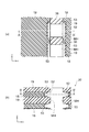
- FIG. 1A and FIG. 1B are cross-sectional views illustrating the semiconductor memory device according to this embodiment.
- 2A and 2B are partially enlarged cross-sectional views illustrating the semiconductor memory device according to this embodiment.
- 1B shows a cross section taken along line AA ′ shown in FIG. 1A
- FIG. 1A shows a cross section taken along line BB ′ shown in FIG. 1B
- FIG. 2B shows a cross section taken along the line AA ′ shown in FIG. 2A
- FIG. 2A shows a cross section taken along the line BB ′ shown in FIG. 2B.
- a silicon substrate 10 is provided in the semiconductor memory device 1 according to the present embodiment.
- an XYZ orthogonal coordinate system is adopted in this specification. Two directions parallel to and orthogonal to the upper surface of the silicon substrate 10 are defined as “X direction” and “Y direction”, and a direction perpendicular to the upper surface is defined as “Z direction”.
- An insulating film 11 made of, for example, silicon oxide, a conductive layer 12 made of, for example, polysilicon, a wiring layer 13 made of, for example, tungsten, and a conductive layer 14 made of, for example, polysilicon are laminated on the silicon substrate 10 in this order.
- a cell source line 15 is formed by the conductive layer 12, the wiring layer 13 and the conductive layer 14. The cell source line 15 extends along the XY plane.
- a plurality of silicon pillars 26 extending in the Z direction are provided on the cell source line 15.
- the lower end of the silicon pillar 26 is connected to the cell source line 15.
- the silicon pillars 26 are arranged in a matrix along the X direction and the Y direction.
- control gate electrodes 33 extending in the Y direction are provided on the cell source line 15.
- the control gate electrodes 33 are arranged in a line along the Z direction on each side in the X direction of the silicon pillars 26 arranged in a line along the Y direction.
- a floating gate electrode 22 is provided between the silicon pillar 26 and the control gate electrode 33.
- the floating gate electrode 22 is disposed at each intersection between the silicon pillar 26 and the control gate electrode 33. That is, a plurality of floating gate electrodes 22 are arranged between the columns of silicon pillars 26 arranged in a line along the Y direction and the rows of control gate electrodes 33 arranged in a line along the Z direction. And they are arranged in a matrix so as to be separated from each other along the Z direction.
- Silicon pillars 26 arranged in a row along the Y direction, control gate electrodes 33 arranged on both sides of the silicon pillars 26 and arranged in a row along the Z direction, and provided between the silicon pillar 26 and the control gate electrode 33, respectively.
- the floating gate electrode 22 constitutes one memory unit MU.
- a plurality of memory units MU are arranged along the X direction.
- two rows of control gate electrodes 33 arranged along the Z direction form one bundle, and a row of silicon pillars 26 arranged in one row along the Y direction is arranged between the bundles.
- the floating gate electrodes 22 arranged in a matrix along the Y direction and the Z direction are arranged between the bundle of control gate electrodes 33 and the columns of the silicon pillars 26.
- the cell source line 15, the silicon pillar 26, the control gate electrode 33, the floating gate electrode 22, and the bit line 36 are filled with an insulating material.
- the silicon pillar 26 is composed of a body silicon 25 serving as a core material and a cover silicon layer 24 surrounding the periphery thereof.
- the silicon pillar 26 is formed of, for example, polysilicon as a whole.
- a tunnel insulating film 23 made of, for example, silicon oxide is provided around the silicon pillar 26.
- an inter-pillar insulating member 38 made of, for example, silicon oxide is provided between the tunnel insulating films 23 adjacent in the Y direction.
- Concave portions 39 extending in the Z direction are formed on the side surfaces of the inter-pillar insulating member 38 facing both sides in the X direction.
- the shape of the recess 39 is, for example, a semi-cylindrical shape with the Z direction as the axial direction.
- Side surfaces of the tunnel insulating film 23 facing both sides in the X direction are in contact with the floating gate electrode 22.
- the floating gate electrode 22 is made of, for example, polysilicon.
- control gate electrode 33 includes a tungsten film 32 and a barrier metal layer 31 provided on the upper surface, the lower surface, and the side surface on the silicon pillar 26 side of the tungsten film 32.
- the barrier metal layer 31 is made of, for example, titanium nitride (TiN).
- a block insulating film 30 is provided between the floating gate electrode 22 and the barrier metal layer 31.
- the block insulating film 30 is also provided on end faces of the floating gate electrode 22 facing both sides in the Y direction.
- a hafnium oxide layer 21, a silicon oxide layer 28, and a hafnium oxide layer 29 are stacked in this order from the floating gate electrode 22 side.
- the block insulating film 30 includes, for example, hafnium oxide and the tunnel insulating film 23 is formed of, for example, silicon oxide, the dielectric constant of the block insulating film 30 is higher than the dielectric constant of the tunnel insulating film 23. high.
- the hafnium oxide layer 21 also extends over the upper and lower surfaces of the floating gate electrode 22.
- the silicon oxide layer 28 and the hafnium oxide layer 29 are also provided between the inter-pillar insulating member 38 and the control gate electrode 33, and are also disposed on the inner surface of the recess 39 of the inter-pillar insulating member 38. .
- the silicon oxide layer 28 and the hafnium oxide layer 29 are also disposed on the upper and lower surfaces of the control gate electrode 33. Further, a part of the control gate electrode 33 is disposed in the recess 39, and is thereby disposed between the silicon pillars 26 adjacent in the Y direction.
- An insulating member 35 made of, for example, silicon oxide is provided between the silicon pillars 26 adjacent in the X direction and between the control gate electrodes 33 adjacent in the X direction.
- a silicon oxide layer 19 as an interlayer insulating film is provided between the control gate electrodes 33 adjacent in the Z direction.
- a memory cell transistor including one floating gate electrode 22 is formed at each intersection between the silicon pillar 26 and the control gate electrode 33.
- a NAND string in which a plurality of memory cell transistors are directly connected is connected between the bit line 36 and the cell source line 15.
- FIG. 3 is a flowchart illustrating the method for manufacturing the semiconductor memory device according to this embodiment.
- 4A to 14B are cross-sectional views illustrating a method for manufacturing the semiconductor memory device according to this embodiment.
- 4 (a) and 4 (b) show the same process, FIG. 4 (b) shows a cross section taken along line AA 'shown in FIG. 4 (a), and FIG. 4 (a) shows FIG. A cross section taken along line BB ′ shown in FIG.
- FIGS. 5A to 14B shows the same process, FIG. 4 (b) shows a cross section taken along line AA 'shown in FIG. 4 (a), and FIG. 4 (a) shows FIG. A cross section taken along line BB ′ shown in FIG. The same applies to FIGS. 5A to 14B.
- a silicon substrate 10 is prepared.
- the insulating film 11, the conductive layer 12, the wiring layer 13, and the conductive layer 14 are formed in this order on the silicon substrate 10.
- a cell source line 15 is formed by the conductive layer 12, the wiring layer 13, and the conductive layer 14.
- silicon nitride layers 18 and silicon oxide layers 19 are alternately stacked on the conductive layer 14 to form an ONON stacked body 20.
- the memory trench MT is formed.
- the conductive layer 14 is exposed on the bottom surface of the memory trench MT.
- the entire memory trench MT is insulated by, for example, silicon oxide by, eg, CVD (Chemical Vapor Deposition) method.
- CVD Chemical Vapor Deposition
- a pattern PAA in which line and space is repeated along the Y direction is formed on the stacked body 20 and the insulating member 38a.
- Each line and each space of the pattern PAA extends in the X direction.
- the insulating members 38a are divided along the Y direction and are arranged intermittently along the Y direction.
- the plurality of inter-pillar insulating members 38 are processed. Thereby, the space after the insulating member 38a in each memory trench MT is removed becomes the memory hole MH. That is, in each memory trench MT, the memory holes MH and the inter-pillar insulating members 38 are alternately arranged along the Y direction.
- the silicon nitride layer 18 is recessed through the memory hole MH, for example, by wet etching using hot phosphoric acid.
- the surface of the side surface of the memory hole MH where the silicon nitride layer 18 is exposed recedes, and a recess 52 is formed between the silicon oxide layers 19.
- the recesses 52 are formed on both sides in the X direction of the memory hole MH, and expand to a part on the side surface of the inter-pillar insulating member 38 facing both sides in the X direction.
- a dummy oxide layer 53 is formed on the exposed surface of the silicon nitride layer 18 by performing, for example, a thermal oxidation process.
- a hafnium oxide layer 21a is formed on the inner surface of the memory hole MH.
- the hafnium oxide layer 21 a is formed so as not to fill the recess 52.
- a silicon film 22a is formed on the hafnium oxide layer 21a.
- the silicon film 22a is formed so as not to fill the memory hole MH.
- the silicon film 22a is etched back by performing anisotropic etching such as RIE, for example.
- anisotropic etching such as RIE, for example.
- the silicon film 22 a is divided for each recess 52.
- the floating gate electrode 22 made of silicon is formed in each recess 52.
- the hafnium oxide layer 21a is etched back.
- the hafnium oxide layer 21 a is divided into the recesses 52 to form the hafnium oxide layer 21.
- anisotropic etching such as wet etching may be performed.
- the tunnel insulating film 23 is formed on the inner surface of the memory hole MH by depositing, for example, silicon oxide.
- a cover silicon layer 24 is formed on the inner surface of the memory hole MH.
- step S12 of FIG. 3 the cover silicon layer 24 and the tunnel insulating film 23 deposited on the bottom surface of the memory hole MH are removed by performing anisotropic etching such as RIE. As a result, the cell source line 15 (see FIG. 4B) is exposed on the bottom surface of the memory hole MH.
- the body silicon 25 is embedded in the memory hole MH by depositing silicon by, for example, the CVD method.
- the body silicon 25 is formed in a pillar shape extending in the Z direction, and its lower end is connected to the cell source line 15.
- the cover silicon layer 24 and the body silicon 25 constitute a silicon pillar 26.
- slits ST extending in the Y direction are formed in the portion between the memory trenches MT in the stacked body 20.
- the silicon nitride layer 18 (FIG. 11B) is formed through the slit ST by, for example, wet etching using hot phosphoric acid. ))).
- the dummy oxide layer 53 and the inter-pillar insulating member 38 function as an etching stopper.
- a recess 55 extending in the Y direction is formed between the silicon oxide layers 19 on both sides in the X direction of the slit ST.
- the dummy oxide layer 53 and the inter-pillar insulating member 38 are exposed on the inner surface of the recess 55.
- the dummy oxide layer 53 (see FIG. 12A) is removed.
- the hafnium oxide layer 21 is exposed on the inner surface of the recess 55.
- the exposed portions of the silicon oxide layer 19 and the inter-pillar insulating member 38 are also recessed, and a recess 39 is formed on the side surface of the inter-pillar insulating member 38 facing the X direction.
- silicon oxide is deposited through the slits ST.
- the silicon oxide layer 28 is formed on the inner surfaces of the slit ST and the recess 55.
- the silicon oxide layer 28 is in contact with the hafnium oxide layer 21 at the back surface of the recess 55. A part of the silicon oxide layer 28 enters the recess 39.
- hafnium oxide is deposited through the slits ST.
- a hafnium oxide layer 29 is formed on the silicon oxide layer 28.
- the hafnium oxide layer 21, the silicon oxide layer 28, and the hafnium oxide layer 29 constitute a block insulating film 30.
- the barrier metal layer 31 is formed on the inner surfaces of the slit ST and the recess 55.
- a tungsten film 32 is formed on the barrier metal layer 31.
- the tungsten film 32 and the barrier metal layer 31 are etched back through the slit ST.
- the control gate electrode 33 is constituted by the barrier metal layer 31 and the tungsten film 32 remaining in each recess 55.
- an insulating member 35 is formed by embedding silicon oxide in the slit ST.
- a plurality of bit lines 36 extending in the X direction are formed on the stacked body 20. Each bit line 36 is connected to the upper end of the silicon pillars 26 arranged in a line along the X direction. In this way, the semiconductor memory device 1 according to this embodiment is manufactured.
- the semiconductor memory device 1 As shown in FIG. 2A, a part of the block insulating film 30 is disposed on the Y direction side of the floating gate electrode 22. As a result, the floating gate electrode 22 is covered with the block insulating film 30 from the three directions on the control gate electrode 33 side in the X direction and on both sides in the Y direction. For this reason, the contact area between the floating gate electrode 22 and the block insulating film 30 is large, and the coupling ratio between the floating gate electrode 22 and the control gate electrode 33 is high. As a result, the semiconductor memory device 1 has good controllability and high operation reliability.
- the recess 39 is formed on the side surface of the inter-pillar insulating member 38 facing the X direction. Is forming.
- the silicon oxide layer 28 and the hafnium oxide layer 29 are also formed on the inner surface of the recess 39, and a part of the control gate electrode 33 is formed in the recess 39. Can enter.
- the control gate electrode 33 is formed so as to cover the floating gate electrode 22, and the coupling ratio between the floating gate electrode 22 and the control gate electrode 33 can be further increased.
- the steps shown in FIGS. 6A and 6B are performed.
- the memory hole MH is formed by embedding the insulating member 38 in the entire memory trench MT and performing etching using the line and space pattern PAA as a mask. For this reason, the miniaturization of the memory hole MH is easy.
- the silicon film 22a is etched and divided into a plurality of floating gate electrodes 22, and thereafter
- the tunnel insulating film 23 and the silicon pillar 26 are formed.
- the tunnel insulating film 23 and the silicon pillar 26 are not formed.
- the tunnel insulating film 23 is not damaged by the etching of the silicon film 22a and a bird's beak is not generated, and the end face of the silicon pillar 26 is not damaged. Therefore, according to this embodiment, the state of the tunnel insulating film 23 and the silicon pillar 26 can be kept good, and the reliability of the semiconductor memory device 1 can be improved.
- FIG. 15 is a cross-sectional view illustrating a semiconductor memory device according to this embodiment.
- the hafnium oxide layer 21 arranged closest to the floating gate electrode 22 among the insulating layers constituting the block insulating film 30 is the silicon pillar 26. It is not divided every time and is continuously provided so as to pass through the side of the plurality of silicon pillars 26 arranged along the Y direction.
- the hafnium oxide layer 21a is not formed in the memory hole MH in the steps shown in FIGS. 8A and 8B, and FIGS. In the step shown in (b), it can be realized by forming the hafnium oxide layer 21 through the slit ST before the silicon oxide layer 28 is formed.
- the hafnium oxide layer 21a is not formed in the memory hole MH in the steps shown in FIGS. 8A and 8B, the memory hole is formed when the silicon film 22a is formed accordingly. MH increases. This facilitates processing of the silicon film 22a in the steps shown in FIGS. 9A and 9B. Further, since the processing for the hafnium oxide layer 21a becomes unnecessary, the manufacturing process can be simplified. Configurations, manufacturing methods, and effects other than those described above in the present embodiment are the same as those in the first embodiment described above.
- FIG. 16A and FIG. 16B are cross-sectional views illustrating the semiconductor memory device according to this embodiment.
- 16B shows a cross section taken along line AA ′ shown in FIG. 16A
- FIG. 16A shows a cross section taken along line BB ′ shown in FIG. 16B.
- a core material 41 made of an insulating material such as silicon oxide is provided inside the silicon pillar 26. ing.
- the core material 41 extends in the Z direction, and its periphery and lower end are covered with the silicon pillar 26.
- the portion of the silicon pillar 26 where the electric field generated from the control gate electrode 33 is difficult to reach is removed, and the control gate electrode 33.
- the control power of the silicon pillar 26 can be increased. Configurations, manufacturing methods, and effects other than those described above in the present embodiment are the same as those in the first embodiment described above.
- FIG. 17 is a cross-sectional view illustrating a semiconductor memory device according to this embodiment.
- the semiconductor memory device 4 according to the present embodiment has an insulating film 11 and a cell source as compared with the semiconductor memory device 1 according to the first embodiment (see FIG. 1B). The difference is that the line 15 is not provided and the silicon pillar 26 is connected to the silicon substrate 10. That is, in the semiconductor memory device 4, the upper layer portion of the silicon substrate 10 functions as a cell source line. Note that a contact layer having an impurity concentration higher than that of the surroundings may be formed in a portion of the silicon substrate 10 to which the silicon pillar 26 is connected. Configurations, manufacturing methods, and effects other than those described above in the present embodiment are the same as those in the first embodiment described above.
- a highly reliable semiconductor memory device and a method for manufacturing the semiconductor memory device can be realized.
Abstract
A semiconductor storage device of an embodiment of the present invention is equipped with a pair of first electrodes, semiconductor pillars, inter-pillar insulation members, a first insulation film, a second electrode, and a second insulation film. The pair of first electrodes extend in a first direction away from one another. The semiconductor pillars and the inter-pillar insulation members are arranged alternately in the first direction between the pair of first electrodes. The semiconductor pillars and the inter-pillar insulation members extend in a second direction that intersects the first direction. The first insulation film is disposed in the periphery of the semiconductor pillars. The second electrode is disposed between each of the pair of first electrodes and the first insulation film. The second electrode is not disposed between the semiconductor pillars and the inter-pillar insulation member. The second insulation film is disposed between the second electrode and the first electrode.
Description
実施形態は、半導体記憶装置及びその製造方法に関する。
Embodiments described herein relate generally to a semiconductor memory device and a method for manufacturing the same.
従来より、NANDフラッシュメモリは、平面構造の微細化により集積度を増加させ、ビットコストを低減させてきたが、平面構造の微細化は限界に近づきつつある。そこで、近年、メモリセルを上下方向に積層する技術が提案されている。しかしながら、このような積層型の記憶装置は製造が困難であり、完成後の製品の信頼性が課題となる。
Conventionally, NAND flash memories have increased the degree of integration by reducing the planar structure and reduced the bit cost, but the miniaturization of the planar structure is approaching the limit. Therefore, in recent years, a technique for stacking memory cells in the vertical direction has been proposed. However, such a stacked memory device is difficult to manufacture, and the reliability of the product after completion becomes a problem.
実施形態の目的は、信頼性が高い半導体記憶装置及びその製造方法を提供することである。
An object of the embodiment is to provide a highly reliable semiconductor memory device and a manufacturing method thereof.
実施形態に係る半導体記憶装置は、一対の第1電極と、半導体ピラーと、ピラー間絶縁部材と、第1絶縁膜と、第2電極と、第2絶縁膜と、を備える。前記一対の第1電極は、相互に離隔して第1方向に延びる。前記半導体ピラー及び前記ピラー間絶縁部材は、前記一対の第1電極間において、前記第1方向に沿って交互に配列されている。前記半導体ピラー及び前記ピラー間絶縁部材は、前記第1方向に対して交差した第2方向に延びる。前記第1絶縁膜は、前記半導体ピラーの周囲に設けられている。前記第2電極は、前記一対の第1電極のそれぞれと前記第1絶縁膜との間に設けられている。前記第2電極は、前記半導体ピラーと前記ピラー間絶縁部材との間には設けられていない。前記第2絶縁膜は、前記第2電極と前記第1電極との間に設けられている。
The semiconductor memory device according to the embodiment includes a pair of first electrodes, a semiconductor pillar, an inter-pillar insulating member, a first insulating film, a second electrode, and a second insulating film. The pair of first electrodes extend in the first direction to be spaced apart from each other. The semiconductor pillars and the inter-pillar insulating members are alternately arranged along the first direction between the pair of first electrodes. The semiconductor pillar and the inter-pillar insulating member extend in a second direction intersecting the first direction. The first insulating film is provided around the semiconductor pillar. The second electrode is provided between each of the pair of first electrodes and the first insulating film. The second electrode is not provided between the semiconductor pillar and the inter-pillar insulating member. The second insulating film is provided between the second electrode and the first electrode.
実施形態に係る半導体記憶装置の製造方法は、層間絶縁膜と第1膜を交互に積層させることにより、積層体を形成する。前記方法は、前記積層体に、前記層間絶縁膜及び前記第1膜の積層方向に対して交差した第1方向に延びるトレンチを形成する。前記方法は、前記トレンチ内に、前記第1方向に沿って相互に離隔した複数のピラー間絶縁部材を形成する。前記方法は、前記トレンチ内における前記ピラー間絶縁部材に挟まれたホールを介して、前記第1膜に対して等方性エッチングを施すことにより、前記層間絶縁膜間に前記ホールに連通した第1凹部を形成する。前記方法は、前記第1凹部の内面上に第1絶縁層を形成すると共に、前記第1凹部内に第2電極を形成する。前記方法は、前記ホールの内面上に第1絶縁膜を形成する。前記方法は、前記第1絶縁膜上に半導体ピラーを形成する。前記方法は、前記積層体における前記トレンチ間の部分に、前記第1方向に延びるスリットを形成する。前記方法は、前記スリットを介して前記第1膜を除去することにより、前記層間絶縁膜間に第2凹部を形成する。前記方法は、前記第2凹部の内面上に第2絶縁層を形成する。前記方法は、前記第2凹部内に第1電極を形成する。
In the manufacturing method of the semiconductor memory device according to the embodiment, the stacked body is formed by alternately stacking the interlayer insulating film and the first film. In the method, a trench extending in a first direction intersecting a stacking direction of the interlayer insulating film and the first film is formed in the stacked body. In the method, a plurality of inter-pillar insulating members spaced apart from each other along the first direction are formed in the trench. In the method, the isotropic etching is performed on the first film through the hole sandwiched between the insulating members between the pillars in the trench, so that the hole communicates with the hole between the interlayer insulating films. 1 recess is formed. In the method, a first insulating layer is formed on the inner surface of the first recess, and a second electrode is formed in the first recess. In the method, a first insulating film is formed on the inner surface of the hole. In the method, a semiconductor pillar is formed on the first insulating film. In the method, slits extending in the first direction are formed in a portion between the trenches in the stacked body. In the method, a second recess is formed between the interlayer insulating films by removing the first film through the slit. The method forms a second insulating layer on the inner surface of the second recess. The method forms a first electrode in the second recess.
以下、図面を参照しつつ、本発明の実施形態について説明する。
先ず、第1の実施形態について説明する。
図1(a)及び図1(b)は、本実施形態に係る半導体記憶装置を例示する断面図である。
図2(a)及び図2(b)は、本実施形態に係る半導体記憶装置を例示する一部拡大断面図である。
なお、図1(b)は図1(a)に示すA-A’線による断面を示し、図1(a)は図1(b)に示すB-B’線による断面を示す。同様に、図2(b)は図2(a)に示すA-A’線による断面を示し、図2(a)は図2(b)に示すB-B’線による断面を示す。 Hereinafter, embodiments of the present invention will be described with reference to the drawings.
First, the first embodiment will be described.
FIG. 1A and FIG. 1B are cross-sectional views illustrating the semiconductor memory device according to this embodiment.
2A and 2B are partially enlarged cross-sectional views illustrating the semiconductor memory device according to this embodiment.
1B shows a cross section taken along line AA ′ shown in FIG. 1A, and FIG. 1A shows a cross section taken along line BB ′ shown in FIG. 1B. Similarly, FIG. 2B shows a cross section taken along the line AA ′ shown in FIG. 2A, and FIG. 2A shows a cross section taken along the line BB ′ shown in FIG. 2B.
図1(a)及び図1(b)に示すように、本実施形態に係る半導体記憶装置1においては、シリコン基板10が設けられている。以下、説明の便宜上、本明細書においては、XYZ直交座標系を採用する。シリコン基板10の上面に対して平行で、且つ、相互に直交する2方向を「X方向」及び「Y方向」とし、上面に対して垂直な方向を「Z方向」とする。
As shown in FIGS. 1A and 1B, in the semiconductor memory device 1 according to the present embodiment, a silicon substrate 10 is provided. Hereinafter, for convenience of explanation, an XYZ orthogonal coordinate system is adopted in this specification. Two directions parallel to and orthogonal to the upper surface of the silicon substrate 10 are defined as “X direction” and “Y direction”, and a direction perpendicular to the upper surface is defined as “Z direction”.
シリコン基板10上には、例えばシリコン酸化物からなる絶縁膜11、例えばポリシリコンからなる導電層12、例えばタングステンからなる配線層13、例えばポリシリコンからなる導電層14がこの順に積層されている。導電層12、配線層13及び導電層14により、セルソース線15が形成されている。セルソース線15は、XY平面に沿って拡がっている。
An insulating film 11 made of, for example, silicon oxide, a conductive layer 12 made of, for example, polysilicon, a wiring layer 13 made of, for example, tungsten, and a conductive layer 14 made of, for example, polysilicon are laminated on the silicon substrate 10 in this order. A cell source line 15 is formed by the conductive layer 12, the wiring layer 13 and the conductive layer 14. The cell source line 15 extends along the XY plane.
セルソース線15上には、Z方向に延びる複数本のシリコンピラー26が設けられている。シリコンピラー26の下端は、セルソース線15に接続されている。シリコンピラー26は、X方向及びY方向に沿ってマトリクス状に配列されている。シリコンピラー26上には、X方向に延びる複数本のビット線36が設けられている。各ビット線36は、X方向に沿って一列に配列された複数本のシリコンピラー26の上端に接続されている。
A plurality of silicon pillars 26 extending in the Z direction are provided on the cell source line 15. The lower end of the silicon pillar 26 is connected to the cell source line 15. The silicon pillars 26 are arranged in a matrix along the X direction and the Y direction. On the silicon pillar 26, a plurality of bit lines 36 extending in the X direction are provided. Each bit line 36 is connected to the upper ends of a plurality of silicon pillars 26 arranged in a line along the X direction.
また、セルソース線15上には、Y方向に延びる複数本の制御ゲート電極33が設けられている。Y方向に沿って一列に配列されたシリコンピラー26のX方向の両側のそれぞれにおいて、制御ゲート電極33は、Z方向に沿って一列に配列されている。
Further, a plurality of control gate electrodes 33 extending in the Y direction are provided on the cell source line 15. The control gate electrodes 33 are arranged in a line along the Z direction on each side in the X direction of the silicon pillars 26 arranged in a line along the Y direction.
シリコンピラー26と制御ゲート電極33との間には、浮遊ゲート電極22が設けられている。浮遊ゲート電極22は、シリコンピラー26と制御ゲート電極33との交差部分毎に配置されている。すなわち、Y方向に沿って一列に配列されたシリコンピラー26の列と、Z方向に沿って一列に配列された制御ゲート電極33の列との間には、複数の浮遊ゲート電極22がY方向及びZ方向に沿って相互に離隔してマトリクス状に配列されている。
A floating gate electrode 22 is provided between the silicon pillar 26 and the control gate electrode 33. The floating gate electrode 22 is disposed at each intersection between the silicon pillar 26 and the control gate electrode 33. That is, a plurality of floating gate electrodes 22 are arranged between the columns of silicon pillars 26 arranged in a line along the Y direction and the rows of control gate electrodes 33 arranged in a line along the Z direction. And they are arranged in a matrix so as to be separated from each other along the Z direction.
Y方向に沿って一列に配列されたシリコンピラー26、その両側に配置され、それぞれZ方向に沿って一列に配列された制御ゲート電極33、シリコンピラー26と制御ゲート電極33との間に設けられた浮遊ゲート電極22により、1つのメモリユニットMUが構成されている。そして、半導体記憶装置1においては、複数のメモリユニットMUが、X方向に沿って配列されている。
Silicon pillars 26 arranged in a row along the Y direction, control gate electrodes 33 arranged on both sides of the silicon pillars 26 and arranged in a row along the Z direction, and provided between the silicon pillar 26 and the control gate electrode 33, respectively. The floating gate electrode 22 constitutes one memory unit MU. In the semiconductor memory device 1, a plurality of memory units MU are arranged along the X direction.
換言すれば、Z方向に沿って配列された二列の制御ゲート電極33が1つの束を構成し、この束間に、Y方向に沿って一列に配列されたシリコンピラー26の列が配置され、制御ゲート電極33の束とシリコンピラー26の列との間に、Y方向及びZ方向に沿ってマトリクス状に配列された浮遊ゲート電極22が配置されている。また、後述するように、セルソース線15、シリコンピラー26、制御ゲート電極33、浮遊ゲート電極22及びビット線36の間は、絶縁材料により埋め込まれている。
In other words, two rows of control gate electrodes 33 arranged along the Z direction form one bundle, and a row of silicon pillars 26 arranged in one row along the Y direction is arranged between the bundles. The floating gate electrodes 22 arranged in a matrix along the Y direction and the Z direction are arranged between the bundle of control gate electrodes 33 and the columns of the silicon pillars 26. As will be described later, the cell source line 15, the silicon pillar 26, the control gate electrode 33, the floating gate electrode 22, and the bit line 36 are filled with an insulating material.
図2(a)及び図2(b)に示すように、シリコンピラー26は、コア材料となるボディシリコン25と、その周囲を囲むカバーシリコン層24とによって構成されている。シリコンピラー26は、全体として例えばポリシリコンにより形成されている。シリコンピラー26の周囲には、例えばシリコン酸化物からなるトンネル絶縁膜23が設けられている。
As shown in FIGS. 2A and 2B, the silicon pillar 26 is composed of a body silicon 25 serving as a core material and a cover silicon layer 24 surrounding the periphery thereof. The silicon pillar 26 is formed of, for example, polysilicon as a whole. A tunnel insulating film 23 made of, for example, silicon oxide is provided around the silicon pillar 26.
Y方向において隣り合うトンネル絶縁膜23間には、例えばシリコン酸化物からなるピラー間絶縁部材38が設けられている。ピラー間絶縁部材38におけるX方向両側に向いた側面には、Z方向に延びる凹部39が形成されている。凹部39の形状は、例えば、Z方向を軸方向とした半円柱形である。
トンネル絶縁膜23におけるX方向両側に向いた側面は、浮遊ゲート電極22に接している。浮遊ゲート電極22は、例えばポリシリコンによって形成されている。 Between thetunnel insulating films 23 adjacent in the Y direction, an inter-pillar insulating member 38 made of, for example, silicon oxide is provided. Concave portions 39 extending in the Z direction are formed on the side surfaces of the inter-pillar insulating member 38 facing both sides in the X direction. The shape of the recess 39 is, for example, a semi-cylindrical shape with the Z direction as the axial direction.
Side surfaces of thetunnel insulating film 23 facing both sides in the X direction are in contact with the floating gate electrode 22. The floating gate electrode 22 is made of, for example, polysilicon.
トンネル絶縁膜23におけるX方向両側に向いた側面は、浮遊ゲート電極22に接している。浮遊ゲート電極22は、例えばポリシリコンによって形成されている。 Between the
Side surfaces of the
一方、制御ゲート電極33は、タングステン膜32と、タングステン膜32の上面上、下面上及びシリコンピラー26側の側面上に設けられたバリアメタル層31によって構成されている。バリアメタル層31は、例えば、チタン窒化物(TiN)によって形成されている。
On the other hand, the control gate electrode 33 includes a tungsten film 32 and a barrier metal layer 31 provided on the upper surface, the lower surface, and the side surface on the silicon pillar 26 side of the tungsten film 32. The barrier metal layer 31 is made of, for example, titanium nitride (TiN).
浮遊ゲート電極22とバリアメタル層31との間には、ブロック絶縁膜30が設けられている。ブロック絶縁膜30は、浮遊ゲート電極22におけるY方向両側に向いた端面上にも設けられている。ブロック絶縁膜30においては、浮遊ゲート電極22側から順に、ハフニウム酸化層21、シリコン酸化層28及びハフニウム酸化層29が積層されている。このように、ブロック絶縁膜30は例えばハフニウム酸化物を含み、トンネル絶縁膜23は例えばシリコン酸化物により形成されているため、ブロック絶縁膜30の誘電率は、トンネル絶縁膜23の誘電率よりも高い。
A block insulating film 30 is provided between the floating gate electrode 22 and the barrier metal layer 31. The block insulating film 30 is also provided on end faces of the floating gate electrode 22 facing both sides in the Y direction. In the block insulating film 30, a hafnium oxide layer 21, a silicon oxide layer 28, and a hafnium oxide layer 29 are stacked in this order from the floating gate electrode 22 side. Thus, since the block insulating film 30 includes, for example, hafnium oxide and the tunnel insulating film 23 is formed of, for example, silicon oxide, the dielectric constant of the block insulating film 30 is higher than the dielectric constant of the tunnel insulating film 23. high.
ハフニウム酸化層21は浮遊ゲート電極22の上面上及び下面上にも回り込んでいる。一方、シリコン酸化層28及びハフニウム酸化層29は、ピラー間絶縁部材38と制御ゲート電極33との間にも設けられており、ピラー間絶縁部材38の凹部39の内面上にも配置されている。また、シリコン酸化層28及びハフニウム酸化層29は、制御ゲート電極33の上面上及び下面上にも配置されている。更に、制御ゲート電極33の一部は、凹部39内に配置され、これにより、Y方向において隣り合うシリコンピラー26間に配置されている。
The hafnium oxide layer 21 also extends over the upper and lower surfaces of the floating gate electrode 22. On the other hand, the silicon oxide layer 28 and the hafnium oxide layer 29 are also provided between the inter-pillar insulating member 38 and the control gate electrode 33, and are also disposed on the inner surface of the recess 39 of the inter-pillar insulating member 38. . The silicon oxide layer 28 and the hafnium oxide layer 29 are also disposed on the upper and lower surfaces of the control gate electrode 33. Further, a part of the control gate electrode 33 is disposed in the recess 39, and is thereby disposed between the silicon pillars 26 adjacent in the Y direction.
X方向において隣り合うシリコンピラー26間であって、X方向において隣り合う制御ゲート電極33間には、例えばシリコン酸化物からなる絶縁部材35が設けられている。また、Z方向において隣り合う制御ゲート電極33間には、層間絶縁膜としてのシリコン酸化層19が設けられている。
An insulating member 35 made of, for example, silicon oxide is provided between the silicon pillars 26 adjacent in the X direction and between the control gate electrodes 33 adjacent in the X direction. A silicon oxide layer 19 as an interlayer insulating film is provided between the control gate electrodes 33 adjacent in the Z direction.
半導体記憶装置1においては、シリコンピラー26と制御ゲート電極33との交差部分毎に、1枚の浮遊ゲート電極22を含むメモリセルトランジスタが形成される。また、ビット線36とセルソース線15との間に、複数のメモリセルトランジスタが直接に接続されたNANDストリングが接続される。
In the semiconductor memory device 1, a memory cell transistor including one floating gate electrode 22 is formed at each intersection between the silicon pillar 26 and the control gate electrode 33. A NAND string in which a plurality of memory cell transistors are directly connected is connected between the bit line 36 and the cell source line 15.
次に、本実施形態に係る半導体記憶装置の製造方法について説明する。
図3は、本実施形態に係る半導体記憶装置の製造方法を例示するフローチャート図である。
図4(a)~図14(b)は、本実施形態に係る半導体記憶装置の製造方法を例示する断面図である。
なお、図4(a)及び図4(b)は同じ工程を示し、図4(b)は図4(a)に示すA-A’線による断面を示し、図4(a)は図4(b)に示すB-B’線による断面を示す。図5(a)~図14(b)についても同様である。 Next, a method for manufacturing the semiconductor memory device according to this embodiment will be described.
FIG. 3 is a flowchart illustrating the method for manufacturing the semiconductor memory device according to this embodiment.
4A to 14B are cross-sectional views illustrating a method for manufacturing the semiconductor memory device according to this embodiment.
4 (a) and 4 (b) show the same process, FIG. 4 (b) shows a cross section taken along line AA 'shown in FIG. 4 (a), and FIG. 4 (a) shows FIG. A cross section taken along line BB ′ shown in FIG. The same applies to FIGS. 5A to 14B.
先ず、図4(a)及び(b)に示すように、シリコン基板10を用意する。
次に、シリコン基板10上に、絶縁膜11、導電層12、配線層13及び導電層14をこの順に形成する。導電層12、配線層13及び導電層14により、セルソース線15が形成される。
次に、図3のステップS1に示すように、導電層14上に、シリコン窒化層18及びシリコン酸化層19を交互に積層し、ONON積層体20を形成する。 First, as shown in FIGS. 4A and 4B, asilicon substrate 10 is prepared.
Next, the insulatingfilm 11, the conductive layer 12, the wiring layer 13, and the conductive layer 14 are formed in this order on the silicon substrate 10. A cell source line 15 is formed by the conductive layer 12, the wiring layer 13, and the conductive layer 14.
Next, as shown in step S <b> 1 of FIG. 3, silicon nitride layers 18 and silicon oxide layers 19 are alternately stacked on theconductive layer 14 to form an ONON stacked body 20.
次に、シリコン基板10上に、絶縁膜11、導電層12、配線層13及び導電層14をこの順に形成する。導電層12、配線層13及び導電層14により、セルソース線15が形成される。
次に、図3のステップS1に示すように、導電層14上に、シリコン窒化層18及びシリコン酸化層19を交互に積層し、ONON積層体20を形成する。 First, as shown in FIGS. 4A and 4B, a
Next, the insulating
Next, as shown in step S <b> 1 of FIG. 3, silicon nitride layers 18 and silicon oxide layers 19 are alternately stacked on the
次に、図5(a)及び図5(b)並びに図3のステップS2に示すように、例えばRIE(Reactive Ion Etching)等の異方性エッチングにより、積層体20にY方向に延びる複数本のメモリトレンチMTを形成する。メモリトレンチMTの底面には導電層14が露出する。
Next, as shown in FIG. 5A, FIG. 5B, and step S2 in FIG. 3, a plurality of pieces extending in the Y direction in the stacked body 20 by anisotropic etching such as RIE (Reactive Ion Etching), for example. The memory trench MT is formed. The conductive layer 14 is exposed on the bottom surface of the memory trench MT.
次に、図6(a)及び図6(b)並びに図3のステップS3に示すように、例えばCVD(Chemical Vapor Deposition)法により、メモリトレンチMT内の全体に、例えばシリコン酸化物からなる絶縁部材38aを埋め込む。
Next, as shown in FIG. 6A, FIG. 6B, and step S3 in FIG. 3, the entire memory trench MT is insulated by, for example, silicon oxide by, eg, CVD (Chemical Vapor Deposition) method. The member 38a is embedded.
次に、図3のステップS4に示すように、積層体20及び絶縁部材38a上に、Y方向に沿ってラインアンドスペースが繰り返されたパターンPAAを形成する。パターンPAAの各ライン及び各スペースは、X方向に延びている。次に、パターンPAA及び最上層のシリコン窒化層18をマスクとしてRIE等の異方性エッチングを施すことにより、絶縁部材38aをY方向に沿って分断し、Y方向に沿って断続的に配列された複数本のピラー間絶縁部材38に加工する。これにより、各メモリトレンチMT内における絶縁部材38aが除去されたあとの空間が、メモリホールMHとなる。すなわち、各メモリトレンチMT内においては、Y方向に沿ってメモリホールMH及びピラー間絶縁部材38が交互に配列される。
Next, as shown in step S4 of FIG. 3, a pattern PAA in which line and space is repeated along the Y direction is formed on the stacked body 20 and the insulating member 38a. Each line and each space of the pattern PAA extends in the X direction. Next, by performing anisotropic etching such as RIE using the pattern PAA and the uppermost silicon nitride layer 18 as a mask, the insulating members 38a are divided along the Y direction and are arranged intermittently along the Y direction. The plurality of inter-pillar insulating members 38 are processed. Thereby, the space after the insulating member 38a in each memory trench MT is removed becomes the memory hole MH. That is, in each memory trench MT, the memory holes MH and the inter-pillar insulating members 38 are alternately arranged along the Y direction.
次に、図7(a)及び図7(b)並びに図3のステップS5に示すように、例えば熱リン酸を用いたウェットエッチングにより、メモリホールMHを介してシリコン窒化層18をリセスする。これにより、メモリホールMHの側面におけるシリコン窒化層18が露出した面が後退し、シリコン酸化層19間に凹部52が形成される。凹部52は、メモリホールMHのX方向両側に形成されると共に、ピラー間絶縁部材38のX方向両側に向いた側面上の一部まで拡大する。
次に、図3のステップS6に示すように、例えば熱酸化処理を施すことにより、シリコン窒化層18の露出面上に、ダミー酸化層53を形成する。 Next, as shown in FIG. 7A, FIG. 7B, and step S5 in FIG. 3, thesilicon nitride layer 18 is recessed through the memory hole MH, for example, by wet etching using hot phosphoric acid. As a result, the surface of the side surface of the memory hole MH where the silicon nitride layer 18 is exposed recedes, and a recess 52 is formed between the silicon oxide layers 19. The recesses 52 are formed on both sides in the X direction of the memory hole MH, and expand to a part on the side surface of the inter-pillar insulating member 38 facing both sides in the X direction.
Next, as shown in step S <b> 6 of FIG. 3, adummy oxide layer 53 is formed on the exposed surface of the silicon nitride layer 18 by performing, for example, a thermal oxidation process.
次に、図3のステップS6に示すように、例えば熱酸化処理を施すことにより、シリコン窒化層18の露出面上に、ダミー酸化層53を形成する。 Next, as shown in FIG. 7A, FIG. 7B, and step S5 in FIG. 3, the
Next, as shown in step S <b> 6 of FIG. 3, a
次に、図8(a)及び図8(b)並びに図3のステップS7に示すように、メモリホールMHの内面上に、ハフニウム酸化層21aを形成する。ハフニウム酸化層21aは、凹部52を埋めきらないように形成する。
次に、図3のステップS8に示すように、ハフニウム酸化層21a上に、シリコン膜22aを形成する。シリコン膜22aは、メモリホールMHを埋めきらないように形成する。 Next, as shown in FIG. 8A, FIG. 8B, and step S7 in FIG. 3, ahafnium oxide layer 21a is formed on the inner surface of the memory hole MH. The hafnium oxide layer 21 a is formed so as not to fill the recess 52.
Next, as shown in step S8 of FIG. 3, asilicon film 22a is formed on the hafnium oxide layer 21a. The silicon film 22a is formed so as not to fill the memory hole MH.
次に、図3のステップS8に示すように、ハフニウム酸化層21a上に、シリコン膜22aを形成する。シリコン膜22aは、メモリホールMHを埋めきらないように形成する。 Next, as shown in FIG. 8A, FIG. 8B, and step S7 in FIG. 3, a
Next, as shown in step S8 of FIG. 3, a
次に、図9(a)及び図9(b)並びに図3のステップS9に示すように、例えばRIE等の異方性エッチングを施すことにより、シリコン膜22aをエッチバックする。これにより、シリコン膜22aが凹部52毎に分断される。この結果、各凹部52内にシリコンからなる浮遊ゲート電極22が形成される。次に、ハフニウム酸化層21aをエッチバックする。これにより、ハフニウム酸化層21aが凹部52毎に分断されて、ハフニウム酸化層21となる。なお、異方性エッチングの替わりに、ウェットエッチング等の等方性エッチングを施してもよい。
Next, as shown in FIG. 9A, FIG. 9B, and step S9 in FIG. 3, the silicon film 22a is etched back by performing anisotropic etching such as RIE, for example. As a result, the silicon film 22 a is divided for each recess 52. As a result, the floating gate electrode 22 made of silicon is formed in each recess 52. Next, the hafnium oxide layer 21a is etched back. As a result, the hafnium oxide layer 21 a is divided into the recesses 52 to form the hafnium oxide layer 21. In place of anisotropic etching, isotropic etching such as wet etching may be performed.
次に、図10(a)及び図10(b)並びに図3のステップS10に示すように、例えばシリコン酸化物を堆積させることにより、メモリホールMHの内面上にトンネル絶縁膜23を形成する。
次に、図3のステップS11に示すように、メモリホールMHの内面上に、カバーシリコン層24を形成する。 Next, as shown in FIG. 10A, FIG. 10B, and step S10 in FIG. 3, thetunnel insulating film 23 is formed on the inner surface of the memory hole MH by depositing, for example, silicon oxide.
Next, as shown in step S11 of FIG. 3, acover silicon layer 24 is formed on the inner surface of the memory hole MH.
次に、図3のステップS11に示すように、メモリホールMHの内面上に、カバーシリコン層24を形成する。 Next, as shown in FIG. 10A, FIG. 10B, and step S10 in FIG. 3, the
Next, as shown in step S11 of FIG. 3, a
次に、図3のステップS12に示すように、RIE等の異方性エッチングを施すことにより、メモリホールMHの底面上に堆積されたカバーシリコン層24及びトンネル絶縁膜23を除去する。これにより、メモリホールMHの底面にセルソース線15(図4(b)参照)が露出する。
Next, as shown in step S12 of FIG. 3, the cover silicon layer 24 and the tunnel insulating film 23 deposited on the bottom surface of the memory hole MH are removed by performing anisotropic etching such as RIE. As a result, the cell source line 15 (see FIG. 4B) is exposed on the bottom surface of the memory hole MH.
次に、図3のステップS13に示すように、例えばCVD法によりシリコンを堆積させることにより、メモリホールMH内にボディシリコン25を埋め込む。ボディシリコン25は、Z方向に延びるピラー状に形成されて、その下端はセルソース線15に接続される。カバーシリコン層24及びボディシリコン25により、シリコンピラー26が構成される。
Next, as shown in step S13 of FIG. 3, the body silicon 25 is embedded in the memory hole MH by depositing silicon by, for example, the CVD method. The body silicon 25 is formed in a pillar shape extending in the Z direction, and its lower end is connected to the cell source line 15. The cover silicon layer 24 and the body silicon 25 constitute a silicon pillar 26.
次に、図11(a)及び図11(b)並びに図3のステップS14に示すように、積層体20におけるメモリトレンチMT間の部分に、Y方向に延びるスリットSTを形成する。
Next, as shown in FIG. 11A, FIG. 11B, and step S14 in FIG. 3, slits ST extending in the Y direction are formed in the portion between the memory trenches MT in the stacked body 20.
次に、図12(a)及び図12(b)並びに図3のステップS15に示すように、例えば熱リン酸を用いたウェットエッチングにより、スリットSTを介してシリコン窒化層18(図11(b)参照)をリセスする。このとき、ダミー酸化層53及びピラー間絶縁部材38がエッチングストッパとして機能する。この結果、スリットSTのX方向両側のシリコン酸化層19間に、Y方向に延びる凹部55が形成される。凹部55の奥面には、ダミー酸化層53及びピラー間絶縁部材38が露出する。
Next, as shown in FIG. 12A, FIG. 12B, and step S15 of FIG. 3, the silicon nitride layer 18 (FIG. 11B) is formed through the slit ST by, for example, wet etching using hot phosphoric acid. ))). At this time, the dummy oxide layer 53 and the inter-pillar insulating member 38 function as an etching stopper. As a result, a recess 55 extending in the Y direction is formed between the silicon oxide layers 19 on both sides in the X direction of the slit ST. The dummy oxide layer 53 and the inter-pillar insulating member 38 are exposed on the inner surface of the recess 55.
次に、図13(a)及び図13(b)並びに図3のステップS16に示すように、ダミー酸化層53(図12(a)参照)を除去する。これにより、凹部55の奥面には、ハフニウム酸化層21が露出する。また、このとき、シリコン酸化層19及びピラー間絶縁部材38の露出部分もリセスされ、ピラー間絶縁部材38におけるX方向に向いた側面に、凹部39が形成される。
Next, as shown in FIGS. 13A and 13B and step S16 in FIG. 3, the dummy oxide layer 53 (see FIG. 12A) is removed. As a result, the hafnium oxide layer 21 is exposed on the inner surface of the recess 55. At this time, the exposed portions of the silicon oxide layer 19 and the inter-pillar insulating member 38 are also recessed, and a recess 39 is formed on the side surface of the inter-pillar insulating member 38 facing the X direction.
次に、図14(a)及び図14(b)並びに図3のステップS17に示すように、スリットSTを介してシリコン酸化物を堆積させる。これにより、スリットST及び凹部55の内面上に、シリコン酸化層28が形成される。シリコン酸化層28は、凹部55の奥面において、ハフニウム酸化層21に接する。また、シリコン酸化層28の一部は、凹部39内に進入する。
Next, as shown in FIGS. 14A and 14B and step S17 in FIG. 3, silicon oxide is deposited through the slits ST. Thereby, the silicon oxide layer 28 is formed on the inner surfaces of the slit ST and the recess 55. The silicon oxide layer 28 is in contact with the hafnium oxide layer 21 at the back surface of the recess 55. A part of the silicon oxide layer 28 enters the recess 39.
次に、図3のステップS18に示すように、スリットSTを介してハフニウム酸化物を堆積させる。これにより、シリコン酸化層28上にハフニウム酸化層29が形成される。ハフニウム酸化層21、シリコン酸化層28及びハフニウム酸化層29により、ブロック絶縁膜30が構成される。
Next, as shown in step S18 of FIG. 3, hafnium oxide is deposited through the slits ST. As a result, a hafnium oxide layer 29 is formed on the silicon oxide layer 28. The hafnium oxide layer 21, the silicon oxide layer 28, and the hafnium oxide layer 29 constitute a block insulating film 30.
次に、図3のステップS19に示すように、スリットST及び凹部55の内面上に、バリアメタル層31を形成する。次に、バリアメタル層31上に、タングステン膜32を形成する。次に、スリットSTを介してタングステン膜32及びバリアメタル層31をエッチバックする。これにより、バリアメタル層31及びタングステン膜32が凹部55毎に分断される。各凹部55内に残留したバリアメタル層31及びタングステン膜32により、制御ゲート電極33が構成される。
Next, as shown in step S <b> 19 of FIG. 3, the barrier metal layer 31 is formed on the inner surfaces of the slit ST and the recess 55. Next, a tungsten film 32 is formed on the barrier metal layer 31. Next, the tungsten film 32 and the barrier metal layer 31 are etched back through the slit ST. As a result, the barrier metal layer 31 and the tungsten film 32 are divided for each recess 55. The control gate electrode 33 is constituted by the barrier metal layer 31 and the tungsten film 32 remaining in each recess 55.
次に、図2(a)及び図2(b)に示すように、スリットST内にシリコン酸化物を埋め込むことにより、絶縁部材35を形成する。
次に、図1(a)及び図1(b)に示すように、積層体20上にX方向に延びる複数本のビット線36を形成する。各ビット線36は、X方向に沿って一列に配列されたシリコンピラー26の上端に接続される。このようにして、本実施形態に係る半導体記憶装置1が製造される。 Next, as shown in FIGS. 2A and 2B, an insulatingmember 35 is formed by embedding silicon oxide in the slit ST.
Next, as shown in FIGS. 1A and 1B, a plurality ofbit lines 36 extending in the X direction are formed on the stacked body 20. Each bit line 36 is connected to the upper end of the silicon pillars 26 arranged in a line along the X direction. In this way, the semiconductor memory device 1 according to this embodiment is manufactured.
次に、図1(a)及び図1(b)に示すように、積層体20上にX方向に延びる複数本のビット線36を形成する。各ビット線36は、X方向に沿って一列に配列されたシリコンピラー26の上端に接続される。このようにして、本実施形態に係る半導体記憶装置1が製造される。 Next, as shown in FIGS. 2A and 2B, an insulating
Next, as shown in FIGS. 1A and 1B, a plurality of
次に、本実施形態の効果について説明する。
本実施形態に係る半導体記憶装置1においては、図2(a)に示すように、ブロック絶縁膜30の一部が、浮遊ゲート電極22のY方向側に配置されている。これにより、浮遊ゲート電極22は、X方向における制御ゲート電極33側及びY方向両側の三方向から、ブロック絶縁膜30によって覆われている。このため、浮遊ゲート電極22とブロック絶縁膜30との接触面積が大きく、浮遊ゲート電極22と制御ゲート電極33との間のカップリング比が高い。この結果、半導体記憶装置1は、制御性が良好であり、動作の信頼性が高い。 Next, the effect of this embodiment will be described.
In thesemiconductor memory device 1 according to the present embodiment, as shown in FIG. 2A, a part of the block insulating film 30 is disposed on the Y direction side of the floating gate electrode 22. As a result, the floating gate electrode 22 is covered with the block insulating film 30 from the three directions on the control gate electrode 33 side in the X direction and on both sides in the Y direction. For this reason, the contact area between the floating gate electrode 22 and the block insulating film 30 is large, and the coupling ratio between the floating gate electrode 22 and the control gate electrode 33 is high. As a result, the semiconductor memory device 1 has good controllability and high operation reliability.
本実施形態に係る半導体記憶装置1においては、図2(a)に示すように、ブロック絶縁膜30の一部が、浮遊ゲート電極22のY方向側に配置されている。これにより、浮遊ゲート電極22は、X方向における制御ゲート電極33側及びY方向両側の三方向から、ブロック絶縁膜30によって覆われている。このため、浮遊ゲート電極22とブロック絶縁膜30との接触面積が大きく、浮遊ゲート電極22と制御ゲート電極33との間のカップリング比が高い。この結果、半導体記憶装置1は、制御性が良好であり、動作の信頼性が高い。 Next, the effect of this embodiment will be described.
In the
また、本実施形態によれば、図13(a)及び図13(b)に示す工程において、カバー酸化膜53を除去するときに、ピラー間絶縁部材38のX方向に向いた側面に凹部39を形成している。これにより、図14(a)及び図14(b)に示す工程において、シリコン酸化層28及びハフニウム酸化層29を凹部39の内面上にも形成し、制御ゲート電極33の一部を凹部39内に進入させることができる。この結果、制御ゲート電極33を浮遊ゲート電極22を覆うように形成し、浮遊ゲート電極22と制御ゲート電極33との間のカップリング比をより一層高めることができる。
Further, according to the present embodiment, when removing the cover oxide film 53 in the step shown in FIGS. 13A and 13B, the recess 39 is formed on the side surface of the inter-pillar insulating member 38 facing the X direction. Is forming. Thus, in the steps shown in FIGS. 14A and 14B, the silicon oxide layer 28 and the hafnium oxide layer 29 are also formed on the inner surface of the recess 39, and a part of the control gate electrode 33 is formed in the recess 39. Can enter. As a result, the control gate electrode 33 is formed so as to cover the floating gate electrode 22, and the coupling ratio between the floating gate electrode 22 and the control gate electrode 33 can be further increased.
更に、本実施形態においては、図5(a)及び図5(b)に示す工程において、積層体20にメモリトレンチMTを形成した後、図6(a)及び図6(b)に示す工程において、メモリトレンチMT内の全体に絶縁部材38を埋め込み、ラインアンドスペース状のパターンPAAをマスクとしてエッチングすることにより、メモリホールMHを形成している。このため、メモリホールMHの微細化が容易である。
Furthermore, in this embodiment, after forming the memory trench MT in the stacked body 20 in the steps shown in FIGS. 5A and 5B, the steps shown in FIGS. 6A and 6B are performed. The memory hole MH is formed by embedding the insulating member 38 in the entire memory trench MT and performing etching using the line and space pattern PAA as a mask. For this reason, the miniaturization of the memory hole MH is easy.
更にまた、図8(a)及び図8(b)並びに図9(a)及び図9(b)に示す工程において、シリコン膜22aをエッチングして複数の浮遊ゲート電極22に分断し、その後、図10(a)及び図10(b)に示す工程において、トンネル絶縁膜23及びシリコンピラー26を形成している。このため、シリコン膜22aをエッチングする際には、トンネル絶縁膜23及びシリコンピラー26は形成されていない。これにより、シリコン膜22aのエッチングにより、トンネル絶縁膜23が損傷を受けてバーズビークが発生することがなく、また、シリコンピラー26の端面が損傷を受けることがない。従って、本実施形態によれば、トンネル絶縁膜23及びシリコンピラー26の状態を良好に保つことができ、半導体記憶装置1の信頼性を高めることができる。
Furthermore, in the steps shown in FIGS. 8A and 8B and FIGS. 9A and 9B, the silicon film 22a is etched and divided into a plurality of floating gate electrodes 22, and thereafter In the steps shown in FIGS. 10A and 10B, the tunnel insulating film 23 and the silicon pillar 26 are formed. For this reason, when the silicon film 22a is etched, the tunnel insulating film 23 and the silicon pillar 26 are not formed. As a result, the tunnel insulating film 23 is not damaged by the etching of the silicon film 22a and a bird's beak is not generated, and the end face of the silicon pillar 26 is not damaged. Therefore, according to this embodiment, the state of the tunnel insulating film 23 and the silicon pillar 26 can be kept good, and the reliability of the semiconductor memory device 1 can be improved.
次に、第2の実施形態について説明する。
図15は、本実施形態に係る半導体記憶装置を例示する断面図である。
図15に示すように、本実施形態に係る半導体記憶装置2においては、ブロック絶縁膜30を構成する絶縁層のうち、最も浮遊ゲート電極22側に配置されたハフニウム酸化層21が、シリコンピラー26毎に分断されておらず、Y方向に沿って配列された複数本のシリコンピラー26の側方を通過するように、連続的に設けられている。 Next, a second embodiment will be described.
FIG. 15 is a cross-sectional view illustrating a semiconductor memory device according to this embodiment.
As shown in FIG. 15, in thesemiconductor memory device 2 according to the present embodiment, the hafnium oxide layer 21 arranged closest to the floating gate electrode 22 among the insulating layers constituting the block insulating film 30 is the silicon pillar 26. It is not divided every time and is continuously provided so as to pass through the side of the plurality of silicon pillars 26 arranged along the Y direction.
図15は、本実施形態に係る半導体記憶装置を例示する断面図である。
図15に示すように、本実施形態に係る半導体記憶装置2においては、ブロック絶縁膜30を構成する絶縁層のうち、最も浮遊ゲート電極22側に配置されたハフニウム酸化層21が、シリコンピラー26毎に分断されておらず、Y方向に沿って配列された複数本のシリコンピラー26の側方を通過するように、連続的に設けられている。 Next, a second embodiment will be described.
FIG. 15 is a cross-sectional view illustrating a semiconductor memory device according to this embodiment.
As shown in FIG. 15, in the
このような構成の半導体記憶装置2は、図8(a)及び図8(b)に示す工程において、メモリホールMH内にハフニウム酸化層21aを形成せずに、図14(a)及び図14(b)に示す工程において、シリコン酸化層28を形成する前に、スリットSTを介してハフニウム酸化層21を形成することにより、実現することができる。
In the semiconductor memory device 2 having such a configuration, the hafnium oxide layer 21a is not formed in the memory hole MH in the steps shown in FIGS. 8A and 8B, and FIGS. In the step shown in (b), it can be realized by forming the hafnium oxide layer 21 through the slit ST before the silicon oxide layer 28 is formed.
本実施形態によれば、図8(a)及び図8(b)に示す工程において、メモリホールMH内にハフニウム酸化層21aを形成しないため、その分、シリコン膜22aを形成するときにメモリホールMHが大きくなる。これにより、図9(a)及び図9(b)に示す工程において、シリコン膜22aに対する加工が容易になる。また、ハフニウム酸化層21aに対する加工が不要となるため、製造工程を簡略化できる。
本実施形態における上記以外の構成、製造方法及び効果は、前述の第1の実施形態と同様である。 According to the present embodiment, since thehafnium oxide layer 21a is not formed in the memory hole MH in the steps shown in FIGS. 8A and 8B, the memory hole is formed when the silicon film 22a is formed accordingly. MH increases. This facilitates processing of the silicon film 22a in the steps shown in FIGS. 9A and 9B. Further, since the processing for the hafnium oxide layer 21a becomes unnecessary, the manufacturing process can be simplified.
Configurations, manufacturing methods, and effects other than those described above in the present embodiment are the same as those in the first embodiment described above.
本実施形態における上記以外の構成、製造方法及び効果は、前述の第1の実施形態と同様である。 According to the present embodiment, since the
Configurations, manufacturing methods, and effects other than those described above in the present embodiment are the same as those in the first embodiment described above.
次に、第3の実施形態について説明する。
図16(a)及び図16(b)は、本実施形態に係る半導体記憶装置を例示する断面図である。
なお、図16(b)は図16(a)に示すA-A’線による断面を示し、図16(a)は図16(b)に示すB-B’線による断面を示す。 Next, a third embodiment will be described.
FIG. 16A and FIG. 16B are cross-sectional views illustrating the semiconductor memory device according to this embodiment.
16B shows a cross section taken along line AA ′ shown in FIG. 16A, and FIG. 16A shows a cross section taken along line BB ′ shown in FIG. 16B.
図16(a)及び図16(b)に示すように、本実施形態に係る半導体記憶装置3においては、シリコンピラー26の内部に、シリコン酸化物等の絶縁材料からなる芯材41が設けられている。芯材41はZ方向に延び、その周囲及び下端はシリコンピラー26によって覆われている。
As shown in FIGS. 16A and 16B, in the semiconductor memory device 3 according to the present embodiment, a core material 41 made of an insulating material such as silicon oxide is provided inside the silicon pillar 26. ing. The core material 41 extends in the Z direction, and its periphery and lower end are covered with the silicon pillar 26.
本実施形態によれば、シリコンピラー26内に絶縁性の芯材41を設けることにより、シリコンピラー26のうち、制御ゲート電極33から発生した電界が到達しにくい部分を除去し、制御ゲート電極33のシリコンピラー26に対する支配力を高めることができる。
本実施形態における上記以外の構成、製造方法及び効果は、前述の第1の実施形態と同様である。 According to the present embodiment, by providing the insulatingcore material 41 in the silicon pillar 26, the portion of the silicon pillar 26 where the electric field generated from the control gate electrode 33 is difficult to reach is removed, and the control gate electrode 33. The control power of the silicon pillar 26 can be increased.
Configurations, manufacturing methods, and effects other than those described above in the present embodiment are the same as those in the first embodiment described above.
本実施形態における上記以外の構成、製造方法及び効果は、前述の第1の実施形態と同様である。 According to the present embodiment, by providing the insulating
Configurations, manufacturing methods, and effects other than those described above in the present embodiment are the same as those in the first embodiment described above.
次に、第4の実施形態について説明する。
図17は、本実施形態に係る半導体記憶装置を例示する断面図である。
図17に示すように、本実施形態に係る半導体記憶装置4は、前述の第1の実施形態に係る半導体記憶装置1(図1(b)参照)と比較して、絶縁膜11及びセルソース線15が設けられておらず、シリコンピラー26がシリコン基板10に接続されている点が異なっている。すなわち、半導体記憶装置4においては、シリコン基板10の上層部分がセルソース線として機能する。なお、シリコン基板10におけるシリコンピラー26が接続される部分には、不純物濃度が周囲よりも高いコンタクト層を形成してもよい。
本実施形態における上記以外の構成、製造方法及び効果は、前述の第1の実施形態と同様である。 Next, a fourth embodiment will be described.
FIG. 17 is a cross-sectional view illustrating a semiconductor memory device according to this embodiment.
As shown in FIG. 17, thesemiconductor memory device 4 according to the present embodiment has an insulating film 11 and a cell source as compared with the semiconductor memory device 1 according to the first embodiment (see FIG. 1B). The difference is that the line 15 is not provided and the silicon pillar 26 is connected to the silicon substrate 10. That is, in the semiconductor memory device 4, the upper layer portion of the silicon substrate 10 functions as a cell source line. Note that a contact layer having an impurity concentration higher than that of the surroundings may be formed in a portion of the silicon substrate 10 to which the silicon pillar 26 is connected.
Configurations, manufacturing methods, and effects other than those described above in the present embodiment are the same as those in the first embodiment described above.
図17は、本実施形態に係る半導体記憶装置を例示する断面図である。
図17に示すように、本実施形態に係る半導体記憶装置4は、前述の第1の実施形態に係る半導体記憶装置1(図1(b)参照)と比較して、絶縁膜11及びセルソース線15が設けられておらず、シリコンピラー26がシリコン基板10に接続されている点が異なっている。すなわち、半導体記憶装置4においては、シリコン基板10の上層部分がセルソース線として機能する。なお、シリコン基板10におけるシリコンピラー26が接続される部分には、不純物濃度が周囲よりも高いコンタクト層を形成してもよい。
本実施形態における上記以外の構成、製造方法及び効果は、前述の第1の実施形態と同様である。 Next, a fourth embodiment will be described.
FIG. 17 is a cross-sectional view illustrating a semiconductor memory device according to this embodiment.
As shown in FIG. 17, the
Configurations, manufacturing methods, and effects other than those described above in the present embodiment are the same as those in the first embodiment described above.
以上説明した実施形態によれば、信頼性が高い半導体記憶装置及びその製造方法を実現することができる。
According to the embodiment described above, a highly reliable semiconductor memory device and a method for manufacturing the semiconductor memory device can be realized.
以上、本発明のいくつかの実施形態を説明したが、これらの実施形態は、例として提示したものであり、発明の範囲を限定することは意図していない。これら新規な実施形態は、その他の様々な形態で実施されることが可能であり、発明の要旨を逸脱しない範囲で、種々の省略、置き換え、変更を行うことができる。これら実施形態やその変形は、発明の範囲や要旨に含まれるとともに、特許請求の範囲に記載された発明及びその等価物の範囲に含まれる。また、前述の各実施形態は、相互に組み合わせて実施することができる。
Although several embodiments of the present invention have been described above, these embodiments are presented as examples and are not intended to limit the scope of the invention. These novel embodiments can be implemented in various other forms, and various omissions, replacements, and changes can be made without departing from the scope of the invention. These embodiments and modifications thereof are included in the scope and gist of the invention, and are included in the scope of the invention described in the claims and the equivalents thereof. Further, the above-described embodiments can be implemented in combination with each other.
Claims (19)
- 相互に離隔して第1方向に延びる一対の第1電極と、
前記一対の第1電極間において、前記第1方向に沿って交互に配列され、前記第1方向に対して交差した第2方向に延びる半導体ピラー及びピラー間絶縁部材と、
前記半導体ピラーの周囲に設けられた第1絶縁膜と、
前記一対の第1電極のそれぞれと前記第1絶縁膜との間に設けられ、前記半導体ピラーと前記ピラー間絶縁部材との間には設けられていない第2電極と、
前記第2電極と前記第1電極との間に設けられた第2絶縁膜と、
を備えた半導体記憶装置。 A pair of first electrodes spaced apart from each other and extending in the first direction;
Between the pair of first electrodes, semiconductor pillars alternately arranged along the first direction and extending in a second direction intersecting the first direction and inter-pillar insulating members;
A first insulating film provided around the semiconductor pillar;
A second electrode provided between each of the pair of first electrodes and the first insulating film, and not provided between the semiconductor pillar and the inter-pillar insulating member;
A second insulating film provided between the second electrode and the first electrode;
A semiconductor memory device. - 前記第2絶縁膜の誘電率は前記第1絶縁膜の誘電率よりも高く、前記第2絶縁膜の一部は、前記第2電極から見て前記第1方向に配置されている請求項1記載の半導体記憶装置。 The dielectric constant of the second insulating film is higher than the dielectric constant of the first insulating film, and a part of the second insulating film is disposed in the first direction when viewed from the second electrode. The semiconductor memory device described.
- 前記第1電極の一部は、前記第2電極から見て前記第1方向に配置されている請求項2記載の半導体記憶装置。 3. The semiconductor memory device according to claim 2, wherein a part of the first electrode is disposed in the first direction when viewed from the second electrode.
- 前記第2絶縁膜は、
その一部が前記第2電極の前記第2方向に向いた面上に配置された第1絶縁層と、
その一部が前記第1電極の前記第2方向に向いた面上に配置された第2絶縁層と、
を有し、
前記第2絶縁層の一部は、前記第1方向に沿って配列された前記第1絶縁膜間に配置された請求項1記載の半導体記憶装置。 The second insulating film is
A first insulating layer, part of which is disposed on a surface of the second electrode facing the second direction;
A second insulating layer, a part of which is disposed on a surface of the first electrode facing the second direction;
Have
The semiconductor memory device according to claim 1, wherein a part of the second insulating layer is disposed between the first insulating films arranged along the first direction. - 前記第2絶縁膜は、
前記第1電極の前記第2方向に向いた面上に配置された第1部分と、
前記第1方向に沿って配列された前記第1絶縁膜間に配置された第2部分と、
を有する請求項1記載の半導体記憶装置。 The second insulating film is
A first portion disposed on a surface of the first electrode facing the second direction;
A second portion disposed between the first insulating films arranged along the first direction;
The semiconductor memory device according to claim 1, comprising: - 前記第1電極の一部は、前記半導体ピラー間に配置されている請求項1記載の半導体記憶装置。 2. The semiconductor memory device according to claim 1, wherein a part of the first electrode is disposed between the semiconductor pillars.
- 前記半導体ピラーから見て前記第2方向に配置された基板と、
前記基板と前記半導体ピラーとの間に設けられ、前記半導体ピラーが接続される第3電極と、
をさらに備えた請求項1記載の半導体記憶装置。 A substrate disposed in the second direction as viewed from the semiconductor pillar;
A third electrode provided between the substrate and the semiconductor pillar to which the semiconductor pillar is connected;
The semiconductor memory device according to claim 1, further comprising: - 前記半導体ピラーから見て前記第2方向に配置され、前記半導体ピラーが接続された半導体基板をさらに備えた請求項1記載の半導体記憶装置。 The semiconductor memory device according to claim 1, further comprising a semiconductor substrate disposed in the second direction as viewed from the semiconductor pillar and connected to the semiconductor pillar.
- 層間絶縁膜と第1膜を交互に積層させることにより、積層体を形成する工程と、
前記積層体に、前記層間絶縁膜及び前記第1膜の積層方向に対して交差した第1方向に延びるトレンチを形成する工程と、
前記トレンチ内に、前記第1方向に沿って相互に離隔した複数のピラー間絶縁部材を形成する工程と、
前記トレンチ内における前記ピラー間絶縁部材に挟まれたホールを介して、前記第1膜に対して等方性エッチングを施すことにより、前記層間絶縁膜間に前記ホールに連通した第1凹部を形成する工程と、
前記第1凹部の内面上に第1絶縁層を形成すると共に、前記第1凹部内に第2電極を形成する工程と、
前記ホールの内面上に第1絶縁膜を形成する工程と、
前記第1絶縁膜上に半導体ピラーを形成する工程と、
前記積層体における前記トレンチ間の部分に、前記第1方向に延びるスリットを形成する工程と、
前記スリットを介して前記第1膜を除去することにより、前記層間絶縁膜間に第2凹部を形成する工程と、
前記第2凹部の内面上に第2絶縁層を形成する工程と、
前記第2凹部内に第1電極を形成する工程と、
を備えた半導体記憶装置の製造方法。 Forming a laminate by alternately laminating interlayer insulating films and first films;
Forming a trench extending in a first direction intersecting a stacking direction of the interlayer insulating film and the first film in the stacked body;
Forming a plurality of inter-pillar insulating members spaced apart from each other along the first direction in the trench;
By forming isotropic etching on the first film through a hole sandwiched between the pillar insulating members in the trench, a first recess communicating with the hole is formed between the interlayer insulating films. And a process of
Forming a first insulating layer on the inner surface of the first recess, and forming a second electrode in the first recess;
Forming a first insulating film on the inner surface of the hole;
Forming a semiconductor pillar on the first insulating film;
Forming a slit extending in the first direction in a portion between the trenches in the stacked body;
Forming a second recess between the interlayer insulating films by removing the first film through the slit;
Forming a second insulating layer on the inner surface of the second recess;
Forming a first electrode in the second recess;
A method for manufacturing a semiconductor memory device comprising: - 前記ピラー間絶縁部材を形成する工程は、
前記トレンチ内の全体に絶縁部材を埋め込む工程と、
前記積層体上に、前記第1方向に沿ってラインアンドスペースが繰り返されるパターンを形成する工程と、
前記パターンをマスクとして異方性エッチングを施すことにより、前記絶縁部材を選択的に除去する工程と、
を有した請求項9記載の半導体記憶装置の製造方法。 The step of forming the inter-pillar insulating member includes
Embedding an insulating member throughout the trench;
Forming a pattern in which line and space is repeated along the first direction on the laminate;
Selectively removing the insulating member by performing anisotropic etching using the pattern as a mask;
10. A method of manufacturing a semiconductor memory device according to claim 9, comprising: - 前記第1凹部を形成する工程において、前記第1凹部を、前記ピラー間絶縁部材における前記第1方向に対して平行な側面上まで拡大する請求項9記載の半導体記憶装置の製造方法。 10. The method of manufacturing a semiconductor memory device according to claim 9, wherein in the step of forming the first recess, the first recess is expanded to a side surface parallel to the first direction of the inter-pillar insulating member.
- 前記第1絶縁層を形成する前に、前記第1凹部の内面上に、組成が前記第1膜の組成とは異なるダミー層を形成する工程と、
前記第2凹部を介して前記ダミー層を除去することにより、前記第2凹部の奥面に前記第1絶縁層を露出させる工程と、
をさらに備え、
前記第2凹部を形成する工程は、前記ダミー層をストッパとして前記第1膜をエッチングする工程を有する請求項9記載の半導体記憶装置の製造方法。 Forming a dummy layer having a composition different from that of the first film on the inner surface of the first recess before forming the first insulating layer;
Removing the dummy layer through the second recess to expose the first insulating layer on the back surface of the second recess;
Further comprising
The method of manufacturing a semiconductor memory device according to claim 9, wherein the step of forming the second concave portion includes a step of etching the first film using the dummy layer as a stopper. - 前記ダミー層を除去するときに、前記ピラー間絶縁部材の側面に第3凹部を形成し、
前記第2絶縁層を形成する工程において、前記第3凹部内にも前記第2絶縁層の一部を配置させる請求項12記載の半導体記憶装置の製造方法。 When removing the dummy layer, forming a third recess in the side surface of the inter-pillar insulating member,
13. The method of manufacturing a semiconductor memory device according to claim 12, wherein in the step of forming the second insulating layer, a part of the second insulating layer is also disposed in the third recess. - 前記第1電極を形成する工程において、前記第3凹部内にも前記第1電極の一部を配置させる請求項13記載の半導体記憶装置の製造方法。 14. The method of manufacturing a semiconductor memory device according to claim 13, wherein in the step of forming the first electrode, a part of the first electrode is also disposed in the third recess.
- 前記第1凹部の内面上に第1絶縁層を形成すると共に、前記第1凹部内に第2電極を形成する工程は、
前記ホール及び前記第1凹部の内面上に前記第1絶縁層を形成する工程と、
前記第1絶縁層上に前記第2電極を形成する工程と、
異方性エッチングを施すことにより、前記第1凹部内に前記第1絶縁層及び前記第2電極を残留させると共に、前記ホール内から前記第1絶縁層及び前記第2電極を除去する工程と、
を有する請求項9記載の半導体記憶装置の製造方法。 Forming a first insulating layer on the inner surface of the first recess and forming a second electrode in the first recess;
Forming the first insulating layer on the inner surface of the hole and the first recess;
Forming the second electrode on the first insulating layer;
Performing anisotropic etching to leave the first insulating layer and the second electrode in the first recess, and removing the first insulating layer and the second electrode from the hole;
A method of manufacturing a semiconductor memory device according to claim 9. - 層間絶縁膜と第1膜を交互に積層させることにより、積層体を形成する工程と、
前記積層体に、前記層間絶縁膜及び前記第1膜の積層方向に対して交差した第1方向に延びるトレンチを形成する工程と、
前記トレンチ内に、前記第1方向に沿って相互に離隔した複数のピラー間絶縁部材を形成する工程と、
前記トレンチ内における前記ピラー間絶縁部材に挟まれたホールを介して、前記第1膜に対して等方性エッチングを施すことにより、前記層間絶縁膜間に前記ホールに連通した第1凹部を形成する工程と、
前記第1凹部内に第2電極を形成する工程と、
前記ホールの内面上に第1絶縁膜を形成する工程と、
前記第1絶縁膜上に半導体ピラーを形成する工程と、
前記積層体における前記トレンチ間の部分に、前記第1方向に延びるスリットを形成する工程と、
前記スリットを介して前記第1膜を除去することにより、前記層間絶縁膜間に第2凹部を形成する工程と、
前記第2凹部の内面上に第2絶縁膜を形成する工程と、
前記第2凹部内に第1電極を形成する工程と、
を備えた半導体記憶装置の製造方法。 Forming a laminate by alternately laminating interlayer insulating films and first films;
Forming a trench extending in a first direction intersecting a stacking direction of the interlayer insulating film and the first film in the stacked body;
Forming a plurality of inter-pillar insulating members spaced apart from each other along the first direction in the trench;
By forming isotropic etching on the first film through a hole sandwiched between the pillar insulating members in the trench, a first recess communicating with the hole is formed between the interlayer insulating films. And a process of
Forming a second electrode in the first recess;
Forming a first insulating film on the inner surface of the hole;
Forming a semiconductor pillar on the first insulating film;
Forming a slit extending in the first direction in a portion between the trenches in the stacked body;
Forming a second recess between the interlayer insulating films by removing the first film through the slit;
Forming a second insulating film on the inner surface of the second recess;
Forming a first electrode in the second recess;
A method for manufacturing a semiconductor memory device comprising: - 前記ピラー間絶縁部材を形成する工程は、
前記トレンチ内の全体に絶縁部材を埋め込む工程と、
前記積層体上に、前記第1方向に沿ってラインアンドスペースが繰り返されるパターンを形成する工程と、
前記パターンをマスクとして異方性エッチングを施すことにより、前記絶縁部材を選択的に除去する工程と、
を有した請求項16記載の半導体記憶装置の製造方法。 The step of forming the inter-pillar insulating member includes
Embedding an insulating member throughout the trench;
Forming a pattern in which line and space is repeated along the first direction on the laminate;
Selectively removing the insulating member by performing anisotropic etching using the pattern as a mask;
The method of manufacturing a semiconductor memory device according to claim 16, comprising: - 前記第1凹部を形成する工程において、前記第1凹部を、前記ピラー間絶縁部材における前記第1方向に対して平行な側面上まで拡大する請求項16記載の半導体記憶装置の製造方法。 17. The method of manufacturing a semiconductor memory device according to claim 16, wherein in the step of forming the first recess, the first recess is expanded to a side surface parallel to the first direction in the inter-pillar insulating member.
- 前記第2電極を形成する前に、前記第1凹部の内面上に、組成が前記第1膜の組成とは異なるカバー層を形成する工程と、
前記第2凹部を介して前記カバー層を除去することにより、前記第2凹部の奥面に前記第2電極を露出させる工程と、
をさらに備え、
前記第2凹部を形成する工程は、前記カバー層をストッパとして前記第1膜をエッチングする工程を有する請求項16記載の半導体記憶装置の製造方法。 Forming a cover layer having a composition different from that of the first film on the inner surface of the first recess before forming the second electrode;
Removing the cover layer through the second recess to expose the second electrode on the back surface of the second recess;
Further comprising
The method of manufacturing a semiconductor memory device according to claim 16, wherein the step of forming the second concave portion includes a step of etching the first film using the cover layer as a stopper.
Priority Applications (4)
| Application Number | Priority Date | Filing Date | Title |
|---|---|---|---|
| CN201580077335.6A CN107533977B (en) | 2015-03-02 | 2015-03-02 | Semiconductor memory device and method of manufacturing the same |
| PCT/JP2015/056102 WO2016139727A1 (en) | 2015-03-02 | 2015-03-02 | Semiconductor storage device and method for manufacturing same |
| TW104107969A TWI596742B (en) | 2015-03-02 | 2015-03-12 | Semiconductor memory device and method of manufacturing the same |
| US15/683,941 US10686045B2 (en) | 2015-03-02 | 2017-08-23 | Semiconductor memory device and method for manufacturing same |
Applications Claiming Priority (1)
| Application Number | Priority Date | Filing Date | Title |
|---|---|---|---|
| PCT/JP2015/056102 WO2016139727A1 (en) | 2015-03-02 | 2015-03-02 | Semiconductor storage device and method for manufacturing same |
Related Child Applications (1)
| Application Number | Title | Priority Date | Filing Date |
|---|---|---|---|
| US15/683,941 Continuation US10686045B2 (en) | 2015-03-02 | 2017-08-23 | Semiconductor memory device and method for manufacturing same |
Publications (1)
| Publication Number | Publication Date |
|---|---|
| WO2016139727A1 true WO2016139727A1 (en) | 2016-09-09 |
Family
ID=56849285
Family Applications (1)
| Application Number | Title | Priority Date | Filing Date |
|---|---|---|---|
| PCT/JP2015/056102 WO2016139727A1 (en) | 2015-03-02 | 2015-03-02 | Semiconductor storage device and method for manufacturing same |
Country Status (4)
| Country | Link |
|---|---|
| US (1) | US10686045B2 (en) |
| CN (1) | CN107533977B (en) |
| TW (1) | TWI596742B (en) |
| WO (1) | WO2016139727A1 (en) |
Cited By (5)
| Publication number | Priority date | Publication date | Assignee | Title |
|---|---|---|---|---|
| US9620515B2 (en) | 2015-05-13 | 2017-04-11 | Kabushiki Kaisha Toshiba | Semiconductor memory device |
| US9837434B2 (en) | 2016-03-14 | 2017-12-05 | Toshiba Memory Corporation | Semiconductor memory device and method for manufacturing same |
| US9847342B2 (en) | 2016-03-14 | 2017-12-19 | Toshiba Memory Corporation | Semiconductor memory device and method for manufacturing same |
| US9966381B2 (en) | 2016-03-18 | 2018-05-08 | Toshiba Memory Corporation | Semiconductor memory device and method for manufacturing the same |
| US11049868B2 (en) | 2015-05-01 | 2021-06-29 | Toshiba Memory Corporation | Stacked type semiconductor memory device |
Families Citing this family (1)
| Publication number | Priority date | Publication date | Assignee | Title |
|---|---|---|---|---|
| JP7189814B2 (en) * | 2019-03-18 | 2022-12-14 | キオクシア株式会社 | semiconductor storage device |
Citations (2)
| Publication number | Priority date | Publication date | Assignee | Title |
|---|---|---|---|---|
| JP2007266143A (en) * | 2006-03-27 | 2007-10-11 | Toshiba Corp | Non-volatile semiconductor memory device and manufacturing method therefor |
| JP2012094694A (en) * | 2010-10-27 | 2012-05-17 | Toshiba Corp | Nonvolatile semiconductor memory device |
Family Cites Families (10)
| Publication number | Priority date | Publication date | Assignee | Title |
|---|---|---|---|---|
| KR101616089B1 (en) * | 2009-06-22 | 2016-04-28 | 삼성전자주식회사 | Three dimensional semiconductor memory device |
| JP5558090B2 (en) * | 2009-12-16 | 2014-07-23 | 株式会社東芝 | Resistance variable memory cell array |
| JP2011165815A (en) * | 2010-02-08 | 2011-08-25 | Toshiba Corp | Nonvolatile semiconductor memory device |
| US9536970B2 (en) * | 2010-03-26 | 2017-01-03 | Samsung Electronics Co., Ltd. | Three-dimensional semiconductor memory devices and methods of fabricating the same |
| US8198672B2 (en) * | 2010-06-30 | 2012-06-12 | SanDisk Technologies, Inc. | Ultrahigh density vertical NAND memory device |
| JP2012069606A (en) | 2010-09-21 | 2012-04-05 | Toshiba Corp | Nonvolatile semiconductor memory device |
| KR101206508B1 (en) * | 2011-03-07 | 2012-11-29 | 에스케이하이닉스 주식회사 | Method for manufacturing 3d-nonvolatile memory device |
| US8803230B2 (en) * | 2012-01-16 | 2014-08-12 | Infineon Technologies Austria Ag | Semiconductor transistor having trench contacts and method for forming therefor |
| US9240416B2 (en) | 2014-06-12 | 2016-01-19 | Kabushiki Kaisha Toshiba | Semiconductor memory device |
| WO2016135849A1 (en) | 2015-02-24 | 2016-09-01 | 株式会社 東芝 | Semiconductor storage device and method for manufacturing same |
-
2015
- 2015-03-02 WO PCT/JP2015/056102 patent/WO2016139727A1/en active Application Filing
- 2015-03-02 CN CN201580077335.6A patent/CN107533977B/en active Active
- 2015-03-12 TW TW104107969A patent/TWI596742B/en active
-
2017
- 2017-08-23 US US15/683,941 patent/US10686045B2/en active Active
Patent Citations (2)
| Publication number | Priority date | Publication date | Assignee | Title |
|---|---|---|---|---|
| JP2007266143A (en) * | 2006-03-27 | 2007-10-11 | Toshiba Corp | Non-volatile semiconductor memory device and manufacturing method therefor |
| JP2012094694A (en) * | 2010-10-27 | 2012-05-17 | Toshiba Corp | Nonvolatile semiconductor memory device |
Cited By (7)
| Publication number | Priority date | Publication date | Assignee | Title |
|---|---|---|---|---|
| US11049868B2 (en) | 2015-05-01 | 2021-06-29 | Toshiba Memory Corporation | Stacked type semiconductor memory device |
| US11943917B2 (en) | 2015-05-01 | 2024-03-26 | Kioxia Corporation | Stacked-type semiconductor memory device |
| US9620515B2 (en) | 2015-05-13 | 2017-04-11 | Kabushiki Kaisha Toshiba | Semiconductor memory device |
| US9837434B2 (en) | 2016-03-14 | 2017-12-05 | Toshiba Memory Corporation | Semiconductor memory device and method for manufacturing same |
| US9847342B2 (en) | 2016-03-14 | 2017-12-19 | Toshiba Memory Corporation | Semiconductor memory device and method for manufacturing same |
| US10418376B2 (en) | 2016-03-14 | 2019-09-17 | Toshiba Memory Corporation | Semiconductor memory device and method for manufacturing same |
| US9966381B2 (en) | 2016-03-18 | 2018-05-08 | Toshiba Memory Corporation | Semiconductor memory device and method for manufacturing the same |
Also Published As
| Publication number | Publication date |
|---|---|
| TWI596742B (en) | 2017-08-21 |
| TW201633506A (en) | 2016-09-16 |
| CN107533977B (en) | 2021-01-08 |
| US20170352735A1 (en) | 2017-12-07 |
| US10686045B2 (en) | 2020-06-16 |
| CN107533977A (en) | 2018-01-02 |
Similar Documents
| Publication | Publication Date | Title |
|---|---|---|
| TWI390714B (en) | Nonvolatile semiconductor memory device and method for manufacturing same | |
| KR101080521B1 (en) | Nonvolatile semiconductor memory device and method for manufacturing same | |
| TWI645549B (en) | Semiconductor memory device and method for manufacturing the same | |
| JP4977180B2 (en) | Method for manufacturing nonvolatile semiconductor memory device | |
| WO2016139727A1 (en) | Semiconductor storage device and method for manufacturing same | |
| TWI640083B (en) | Semiconductor memory device and method for manufacturing same | |
| TWI647817B (en) | Semiconductor memory device and manufacturing method thereof | |
| WO2016194211A1 (en) | Semiconductor storage device and manufacturing method therefor | |
| US9837434B2 (en) | Semiconductor memory device and method for manufacturing same | |
| TWI578449B (en) | Nonvolatile semiconductor memory device and manufacturing method thereof | |
| US20130032874A1 (en) | Method for manufacturing nonvolatile semiconductor memory device and nonvolatile semiconductor memory device | |
| TWI663716B (en) | Semiconductor device and manufacturing method thereof | |
| JP2010045314A (en) | Nonvolatile semiconductor memory device and method for manufacturing same | |
| TWI591770B (en) | Semiconductor memory device and method of manufacturing the same | |
| JP2011108921A (en) | Non-volatile semiconductor memory device, and method for manufacturing the same | |
| TWI698004B (en) | Semiconductor memory device | |
| US10083983B2 (en) | Semiconductor memory device | |
| TW201818508A (en) | Semiconductor memory device | |
| US20170194345A1 (en) | Semiconductor memory device and method for manufacturing the same | |
| JP2019050243A (en) | Semiconductor storage and manufacturing method therefor | |
| US9735167B2 (en) | Semiconductor memory device and method for manufacturing the same | |
| JP6762897B2 (en) | Semiconductor storage device and its manufacturing method | |
| JP2021048297A (en) | Semiconductor memory device | |
| JP2020043277A (en) | Semiconductor storage | |
| JP2014187189A (en) | Semiconductor storage device and manufacturing method of the same |
Legal Events
| Date | Code | Title | Description |
|---|---|---|---|
| 121 | Ep: the epo has been informed by wipo that ep was designated in this application |
Ref document number: 15883897 Country of ref document: EP Kind code of ref document: A1 |
|
| NENP | Non-entry into the national phase |
Ref country code: DE |
|
| 122 | Ep: pct application non-entry in european phase |
Ref document number: 15883897 Country of ref document: EP Kind code of ref document: A1 |
|
| NENP | Non-entry into the national phase |
Ref country code: JP |