US9735167B2 - Semiconductor memory device and method for manufacturing the same - Google Patents
Semiconductor memory device and method for manufacturing the same Download PDFInfo
- Publication number
- US9735167B2 US9735167B2 US14/840,345 US201514840345A US9735167B2 US 9735167 B2 US9735167 B2 US 9735167B2 US 201514840345 A US201514840345 A US 201514840345A US 9735167 B2 US9735167 B2 US 9735167B2
- Authority
- US
- United States
- Prior art keywords
- interconnects
- disposed
- extending
- interconnect
- insulating member
- Prior art date
- Legal status (The legal status is an assumption and is not a legal conclusion. Google has not performed a legal analysis and makes no representation as to the accuracy of the status listed.)
- Active, expires
Links
- 239000004065 semiconductor Substances 0.000 title claims abstract description 65
- 238000004519 manufacturing process Methods 0.000 title claims description 9
- 238000000034 method Methods 0.000 title description 11
- 239000010410 layer Substances 0.000 claims description 145
- 239000000758 substrate Substances 0.000 claims description 23
- 239000011229 interlayer Substances 0.000 claims description 11
- 238000005530 etching Methods 0.000 claims description 6
- 239000004020 conductor Substances 0.000 claims description 3
- XUIMIQQOPSSXEZ-UHFFFAOYSA-N Silicon Chemical compound [Si] XUIMIQQOPSSXEZ-UHFFFAOYSA-N 0.000 description 62
- 229910052710 silicon Inorganic materials 0.000 description 61
- 239000010703 silicon Substances 0.000 description 61
- VYPSYNLAJGMNEJ-UHFFFAOYSA-N Silicium dioxide Chemical compound O=[Si]=O VYPSYNLAJGMNEJ-UHFFFAOYSA-N 0.000 description 27
- 229910052814 silicon oxide Inorganic materials 0.000 description 27
- 229910052751 metal Inorganic materials 0.000 description 13
- 239000002184 metal Substances 0.000 description 13
- 230000008878 coupling Effects 0.000 description 11
- 238000010168 coupling process Methods 0.000 description 11
- 238000005859 coupling reaction Methods 0.000 description 11
- 230000004888 barrier function Effects 0.000 description 10
- 230000002093 peripheral effect Effects 0.000 description 10
- 229910052581 Si3N4 Inorganic materials 0.000 description 6
- 238000000151 deposition Methods 0.000 description 6
- 239000000463 material Substances 0.000 description 6
- HQVNEWCFYHHQES-UHFFFAOYSA-N silicon nitride Chemical compound N12[Si]34N5[Si]62N3[Si]51N64 HQVNEWCFYHHQES-UHFFFAOYSA-N 0.000 description 6
- 230000010354 integration Effects 0.000 description 5
- NBIIXXVUZAFLBC-UHFFFAOYSA-N Phosphoric acid Chemical compound OP(O)(O)=O NBIIXXVUZAFLBC-UHFFFAOYSA-N 0.000 description 4
- TWNQGVIAIRXVLR-UHFFFAOYSA-N oxo(oxoalumanyloxy)alumane Chemical compound O=[Al]O[Al]=O TWNQGVIAIRXVLR-UHFFFAOYSA-N 0.000 description 4
- 238000001020 plasma etching Methods 0.000 description 4
- 238000000231 atomic layer deposition Methods 0.000 description 3
- 230000000694 effects Effects 0.000 description 3
- 230000008569 process Effects 0.000 description 3
- 238000001039 wet etching Methods 0.000 description 3
- NRTOMJZYCJJWKI-UHFFFAOYSA-N Titanium nitride Chemical compound [Ti]#N NRTOMJZYCJJWKI-UHFFFAOYSA-N 0.000 description 2
- 229910000147 aluminium phosphate Inorganic materials 0.000 description 2
- 238000005229 chemical vapour deposition Methods 0.000 description 2
- CJNBYAVZURUTKZ-UHFFFAOYSA-N hafnium(iv) oxide Chemical compound O=[Hf]=O CJNBYAVZURUTKZ-UHFFFAOYSA-N 0.000 description 2
- 238000001459 lithography Methods 0.000 description 2
- WFKWXMTUELFFGS-UHFFFAOYSA-N tungsten Chemical compound [W] WFKWXMTUELFFGS-UHFFFAOYSA-N 0.000 description 2
- 229910052721 tungsten Inorganic materials 0.000 description 2
- 239000010937 tungsten Substances 0.000 description 2
- KJTLSVCANCCWHF-UHFFFAOYSA-N Ruthenium Chemical compound [Ru] KJTLSVCANCCWHF-UHFFFAOYSA-N 0.000 description 1
- 230000008901 benefit Effects 0.000 description 1
- OEYIOHPDSNJKLS-UHFFFAOYSA-N choline Chemical compound C[N+](C)(C)CCO OEYIOHPDSNJKLS-UHFFFAOYSA-N 0.000 description 1
- 229960001231 choline Drugs 0.000 description 1
- 238000001312 dry etching Methods 0.000 description 1
- 230000006870 function Effects 0.000 description 1
- 238000010438 heat treatment Methods 0.000 description 1
- 239000011810 insulating material Substances 0.000 description 1
- 239000011159 matrix material Substances 0.000 description 1
- 230000004048 modification Effects 0.000 description 1
- 238000012986 modification Methods 0.000 description 1
- 238000007254 oxidation reaction Methods 0.000 description 1
- 229910021420 polycrystalline silicon Inorganic materials 0.000 description 1
- 229920005591 polysilicon Polymers 0.000 description 1
- 229910052707 ruthenium Inorganic materials 0.000 description 1
- 239000002356 single layer Substances 0.000 description 1
- 239000000126 substance Substances 0.000 description 1
- 238000006467 substitution reaction Methods 0.000 description 1
- XLYOFNOQVPJJNP-UHFFFAOYSA-N water Substances O XLYOFNOQVPJJNP-UHFFFAOYSA-N 0.000 description 1
Images


Classifications
-
- H—ELECTRICITY
- H10—SEMICONDUCTOR DEVICES; ELECTRIC SOLID-STATE DEVICES NOT OTHERWISE PROVIDED FOR
- H10B—ELECTRONIC MEMORY DEVICES
- H10B41/00—Electrically erasable-and-programmable ROM [EEPROM] devices comprising floating gates
- H10B41/20—Electrically erasable-and-programmable ROM [EEPROM] devices comprising floating gates characterised by three-dimensional arrangements, e.g. with cells on different height levels
- H10B41/23—Electrically erasable-and-programmable ROM [EEPROM] devices comprising floating gates characterised by three-dimensional arrangements, e.g. with cells on different height levels with source and drain on different levels, e.g. with sloping channels
- H10B41/27—Electrically erasable-and-programmable ROM [EEPROM] devices comprising floating gates characterised by three-dimensional arrangements, e.g. with cells on different height levels with source and drain on different levels, e.g. with sloping channels the channels comprising vertical portions, e.g. U-shaped channels
-
- H01L27/11556—
-
- H—ELECTRICITY
- H01—ELECTRIC ELEMENTS
- H01L—SEMICONDUCTOR DEVICES NOT COVERED BY CLASS H10
- H01L21/00—Processes or apparatus adapted for the manufacture or treatment of semiconductor or solid state devices or of parts thereof
- H01L21/70—Manufacture or treatment of devices consisting of a plurality of solid state components formed in or on a common substrate or of parts thereof; Manufacture of integrated circuit devices or of parts thereof
- H01L21/71—Manufacture of specific parts of devices defined in group H01L21/70
- H01L21/768—Applying interconnections to be used for carrying current between separate components within a device comprising conductors and dielectrics
- H01L21/76838—Applying interconnections to be used for carrying current between separate components within a device comprising conductors and dielectrics characterised by the formation and the after-treatment of the conductors
- H01L21/76885—By forming conductive members before deposition of protective insulating material, e.g. pillars, studs
-
- H—ELECTRICITY
- H01—ELECTRIC ELEMENTS
- H01L—SEMICONDUCTOR DEVICES NOT COVERED BY CLASS H10
- H01L23/00—Details of semiconductor or other solid state devices
- H01L23/52—Arrangements for conducting electric current within the device in operation from one component to another, i.e. interconnections, e.g. wires, lead frames
- H01L23/522—Arrangements for conducting electric current within the device in operation from one component to another, i.e. interconnections, e.g. wires, lead frames including external interconnections consisting of a multilayer structure of conductive and insulating layers inseparably formed on the semiconductor body
- H01L23/5226—Via connections in a multilevel interconnection structure
-
- H—ELECTRICITY
- H01—ELECTRIC ELEMENTS
- H01L—SEMICONDUCTOR DEVICES NOT COVERED BY CLASS H10
- H01L23/00—Details of semiconductor or other solid state devices
- H01L23/52—Arrangements for conducting electric current within the device in operation from one component to another, i.e. interconnections, e.g. wires, lead frames
- H01L23/522—Arrangements for conducting electric current within the device in operation from one component to another, i.e. interconnections, e.g. wires, lead frames including external interconnections consisting of a multilayer structure of conductive and insulating layers inseparably formed on the semiconductor body
- H01L23/528—Geometry or layout of the interconnection structure
-
- H01L27/1052—
-
- H01L27/11517—
-
- H01L27/11521—
-
- H01L27/11524—
-
- H01L27/11529—
-
- H01L27/11548—
-
- H01L27/11551—
-
- H01L27/11568—
-
- H01L27/1157—
-
- H01L27/11573—
-
- H01L27/11578—
-
- H01L27/2481—
-
- H—ELECTRICITY
- H01—ELECTRIC ELEMENTS
- H01L—SEMICONDUCTOR DEVICES NOT COVERED BY CLASS H10
- H01L29/00—Semiconductor devices adapted for rectifying, amplifying, oscillating or switching, or capacitors or resistors with at least one potential-jump barrier or surface barrier, e.g. PN junction depletion layer or carrier concentration layer; Details of semiconductor bodies or of electrodes thereof ; Multistep manufacturing processes therefor
- H01L29/66—Types of semiconductor device ; Multistep manufacturing processes therefor
- H01L29/68—Types of semiconductor device ; Multistep manufacturing processes therefor controllable by only the electric current supplied, or only the electric potential applied, to an electrode which does not carry the current to be rectified, amplified or switched
- H01L29/76—Unipolar devices, e.g. field effect transistors
- H01L29/772—Field effect transistors
- H01L29/78—Field effect transistors with field effect produced by an insulated gate
- H01L29/788—Field effect transistors with field effect produced by an insulated gate with floating gate
- H01L29/7889—Vertical transistors, i.e. transistors having source and drain not in the same horizontal plane
-
- H—ELECTRICITY
- H10—SEMICONDUCTOR DEVICES; ELECTRIC SOLID-STATE DEVICES NOT OTHERWISE PROVIDED FOR
- H10B—ELECTRONIC MEMORY DEVICES
- H10B41/00—Electrically erasable-and-programmable ROM [EEPROM] devices comprising floating gates
-
- H—ELECTRICITY
- H10—SEMICONDUCTOR DEVICES; ELECTRIC SOLID-STATE DEVICES NOT OTHERWISE PROVIDED FOR
- H10B—ELECTRONIC MEMORY DEVICES
- H10B41/00—Electrically erasable-and-programmable ROM [EEPROM] devices comprising floating gates
- H10B41/20—Electrically erasable-and-programmable ROM [EEPROM] devices comprising floating gates characterised by three-dimensional arrangements, e.g. with cells on different height levels
-
- H—ELECTRICITY
- H10—SEMICONDUCTOR DEVICES; ELECTRIC SOLID-STATE DEVICES NOT OTHERWISE PROVIDED FOR
- H10B—ELECTRONIC MEMORY DEVICES
- H10B41/00—Electrically erasable-and-programmable ROM [EEPROM] devices comprising floating gates
- H10B41/30—Electrically erasable-and-programmable ROM [EEPROM] devices comprising floating gates characterised by the memory core region
- H10B41/35—Electrically erasable-and-programmable ROM [EEPROM] devices comprising floating gates characterised by the memory core region with a cell select transistor, e.g. NAND
-
- H—ELECTRICITY
- H10—SEMICONDUCTOR DEVICES; ELECTRIC SOLID-STATE DEVICES NOT OTHERWISE PROVIDED FOR
- H10B—ELECTRONIC MEMORY DEVICES
- H10B41/00—Electrically erasable-and-programmable ROM [EEPROM] devices comprising floating gates
- H10B41/40—Electrically erasable-and-programmable ROM [EEPROM] devices comprising floating gates characterised by the peripheral circuit region
- H10B41/41—Electrically erasable-and-programmable ROM [EEPROM] devices comprising floating gates characterised by the peripheral circuit region of a memory region comprising a cell select transistor, e.g. NAND
-
- H—ELECTRICITY
- H10—SEMICONDUCTOR DEVICES; ELECTRIC SOLID-STATE DEVICES NOT OTHERWISE PROVIDED FOR
- H10B—ELECTRONIC MEMORY DEVICES
- H10B41/00—Electrically erasable-and-programmable ROM [EEPROM] devices comprising floating gates
- H10B41/50—Electrically erasable-and-programmable ROM [EEPROM] devices comprising floating gates characterised by the boundary region between the core region and the peripheral circuit region
-
- H—ELECTRICITY
- H10—SEMICONDUCTOR DEVICES; ELECTRIC SOLID-STATE DEVICES NOT OTHERWISE PROVIDED FOR
- H10B—ELECTRONIC MEMORY DEVICES
- H10B43/00—EEPROM devices comprising charge-trapping gate insulators
- H10B43/20—EEPROM devices comprising charge-trapping gate insulators characterised by three-dimensional arrangements, e.g. with cells on different height levels
-
- H—ELECTRICITY
- H10—SEMICONDUCTOR DEVICES; ELECTRIC SOLID-STATE DEVICES NOT OTHERWISE PROVIDED FOR
- H10B—ELECTRONIC MEMORY DEVICES
- H10B43/00—EEPROM devices comprising charge-trapping gate insulators
- H10B43/30—EEPROM devices comprising charge-trapping gate insulators characterised by the memory core region
- H10B43/35—EEPROM devices comprising charge-trapping gate insulators characterised by the memory core region with cell select transistors, e.g. NAND
-
- H—ELECTRICITY
- H10—SEMICONDUCTOR DEVICES; ELECTRIC SOLID-STATE DEVICES NOT OTHERWISE PROVIDED FOR
- H10B—ELECTRONIC MEMORY DEVICES
- H10B43/00—EEPROM devices comprising charge-trapping gate insulators
- H10B43/40—EEPROM devices comprising charge-trapping gate insulators characterised by the peripheral circuit region
-
- H—ELECTRICITY
- H10—SEMICONDUCTOR DEVICES; ELECTRIC SOLID-STATE DEVICES NOT OTHERWISE PROVIDED FOR
- H10B—ELECTRONIC MEMORY DEVICES
- H10B63/00—Resistance change memory devices, e.g. resistive RAM [ReRAM] devices
- H10B63/80—Arrangements comprising multiple bistable or multi-stable switching components of the same type on a plane parallel to the substrate, e.g. cross-point arrays
- H10B63/84—Arrangements comprising multiple bistable or multi-stable switching components of the same type on a plane parallel to the substrate, e.g. cross-point arrays arranged in a direction perpendicular to the substrate, e.g. 3D cell arrays
-
- H—ELECTRICITY
- H10—SEMICONDUCTOR DEVICES; ELECTRIC SOLID-STATE DEVICES NOT OTHERWISE PROVIDED FOR
- H10B—ELECTRONIC MEMORY DEVICES
- H10B99/00—Subject matter not provided for in other groups of this subclass
-
- H—ELECTRICITY
- H10—SEMICONDUCTOR DEVICES; ELECTRIC SOLID-STATE DEVICES NOT OTHERWISE PROVIDED FOR
- H10B—ELECTRONIC MEMORY DEVICES
- H10B41/00—Electrically erasable-and-programmable ROM [EEPROM] devices comprising floating gates
- H10B41/10—Electrically erasable-and-programmable ROM [EEPROM] devices comprising floating gates characterised by the top-view layout
Definitions
- Embodiments described herein relate generally to a semiconductor memory device and a method for manufacturing the same.
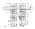
- FIG. 1 is a plan view showing a semiconductor memory device according to a first embodiment
- FIG. 2 is a sectional view taken along line A-A′ in FIG. 1 ;
- FIG. 3 is a sectional view taken along line B-B′ in FIG. 1 ;
- FIGS. 4A and 4B are sectional views showing the semiconductor memory device according to the first embodiment
- FIGS. 5A to 13B are sectional views showing a manufacturing method for the semiconductor memory device according to the first embodiment
- FIG. 14 is a plan view showing a semiconductor memory device according to a second embodiment
- FIG. 15 is a sectional view taken along line E-E′ in FIG. 14 ;
- FIG. 16 is a sectional view showing a semiconductor memory device according to a third embodiment.
- a semiconductor memory device includes a plurality of first interconnects extending in a first direction and arrayed along a second direction crossing the first direction, a plurality of semiconductor pillars arrayed in a row along the first direction in each of spaces among the first interconnects and extending in a third direction crossing the first direction and the second direction, a first electrode disposed between one of the semiconductor pillars and one of the first interconnects, a first insulating film disposed between the first electrode and one of the first interconnects, and a first insulating member disposed between the semiconductor pillars in the first direction, extending in the third direction and opposed the first interconnects not via the first insulating film.
- FIG. 1 is a plan view showing a semiconductor memory device according to the embodiment.
- FIG. 2 is a sectional view taken along line A-A′ in FIG. 1 .
- FIG. 3 is a sectional view taken along line B-B′ in FIG. 1 .
- FIGS. 4A and 4B are sectional views showing the semiconductor memory device according to the embodiment.
- FIG. 4B shows a cross section taken along line C-C′ in FIG. 4A .
- FIG. 4A shows a cross section taken along line D-D′ in FIG. 4B .
- FIGS. 1 to 3 for convenience of illustration, only a part of a plurality of members is shown and the remaining part is omitted.
- components in an upper layer e.g., upper layer interconnects 44 and 48
- components in an intermediate layer e.g., intermediate interconnects 42 and 46
- components in a lower layer e.g., a stacked body 20
- Components seen from the upward direction are indicated by solid lines.
- Components in the immediately below stage hidden by the components are indicated by broken lines. Components below the components are omitted.
- a silicon substrate 10 is provided in a semiconductor memory device 1 according to the embodiment.
- a memory region Rm, interconnect lead regions Rd, and peripheral circuit regions Rc are set.
- the interconnect lead regions Rd are disposed on both sides in the X-direction of the memory region Rm.
- the peripheral circuit regions Rc are disposed around the memory region Rm and the interconnect lead regions Rd. Peripheral circuits are formed in the peripheral circuit regions Rc. The peripheral circuits input signals to and output signals from memory cells to thereby operate the memory cells.
- the interconnect lead regions Rd are regions for drawing out, from the memory region Rm, interconnects extending in the X-direction and connecting the interconnects to the peripheral circuits.
- the memory region Rm and the interconnect lead regions Rd are sectioned into a plurality of blocks arrayed along the Y-direction.
- boundary lines IB among the blocks are indicated by alternate long and two short dashes lines. The same applies to FIG. 14 referred to below.
- one lower selection gate interconnect layer 21 On the silicon substrate 10 , for example, one lower selection gate interconnect layer 21 , a plurality of word line interconnect layers 22 , and one or more, for example, two upper selection gate interconnect layers 23 are spaced from one another via interlayer insulating films 31 and stacked to configure the stacked body 20 .
- the shape of the stacked body 20 In the memory region Rm, all layers of the stacked body 20 are disposed.
- the shape of the stacked body 20 In the interconnect lead regions Rd, the shape of the stacked body 20 is a step shape.
- the stacked body 20 is drawn further to the outer side toward a lower stage. That is, the word line interconnect layers 22 and the upper selection gate interconnect layers 23 are not disposed in regions right above both end portions in the X-direction of the lower selection gate interconnect layer 21 .
- the word line interconnect layers 22 in upper stages of the word line interconnect layer 22 and the upper selection gate interconnect layers 23 are not disposed. In regions right above both end portions in the X-direction of the word line interconnect layers 22 in the top stage, the upper selection gate interconnect layers 23 are not disposed.
- a plurality of linear memory trenches MT extending in the X-direction are formed.
- the memory trenches MT pierce through the stacked body 20 in the Z-direction and reach the silicon substrate 10 .
- the memory trenches MT also pierce through the stacked body 20 in the X-direction. Therefore, the memory trenches MT divide the upper selection gate interconnect layers 23 , the word line interconnect layers 22 , and the lower selection gate interconnect layer 21 .
- portions sandwiched by the memory trenches MT adjacent to each other in the upper selection gate interconnect layers 23 are upper selection gate lines 23 a extending in the X-direction.
- portions sandwiched by the memory trenches MT are respectively word lines 22 a and lower selection gate lines 21 a.
- a plurality of silicon pillars 26 are arrayed in rows along the X-direction. Therefore, the lower selection gate lines 21 a, the word lines 22 a, and the upper selection gate lines 23 a are disposed on both sides in the Y-direction of the silicon pillars 26 .
- the shape of the silicon pillars 26 is, for example, a quadratic prism shape extending in the Z-direction.
- the lower ends of the silicon pillars 26 are connected to the silicon substrate 10 .
- Insulating members 32 made of, for example, silicon oxide are provided among the silicon pillars 26 in the memory trenches MT.
- through-holes SH extending in the Z-direction are discontinuously formed in the X-direction.
- through-hole SH in one place is formed for every ten silicon pillars 26 .
- the through-holes SH pierce through the stacked body 20 in the Z-direction and reach the silicon substrate 10 .
- insulating members 33 made of, for example, silicon oxide are embedded in the through-holes SH.
- the memory region Rm is described.
- Bit line plugs 27 are provided on the silicon pillars 26 .
- a plurality of bit lines 28 extending in the Y-direction are provided on the bit line plugs 27 .
- the silicon pillars 26 are connected to the bit lines 28 via the bit line plugs 27 .
- the bit lines 28 are connected to, for example, a sense amplifier of the peripheral circuit.
- an interlayer insulating film 30 made of, for example, silicon oxide is provided on the stacked body 20 .
- the bit line plugs 27 and the bit lines 28 are embedded in the interlayer insulating film 30 .
- FIGS. 4A and 4B are partial sectional views showing small portions including one silicon pillar 26 and the through-hole SH in one place in th semiconductor memory device 1 .
- a tunnel insulating film 36 is provided around the silicon pillar 26 when viewed from the Z-direction.
- the tunnel insulating film 36 is a film that feeds a tunnel current when a predetermined voltage within a range of a driving voltage of the semiconductor memory device 1 is applied to the tunnel insulating film 36 .
- the tunnel insulating film 36 is, for example, a silicon oxide film of a single layer or a three-layer film consisting of a silicon oxide layer, a silicon nitride layer, and a silicon oxide layer.
- a floating gate electrode 29 is provided between the tunnel insulating film 36 and the word line 22 a.
- the floating gate electrode 29 is a conductive member that accumulates electric charges and is formed of, for example, polysilicon (Si).
- a high dielectric constant layer 37 a made of a high dielectric constant material such as silicon nitride (SiN), hafnium oxide (HfO 2 ), or aluminum oxide (Al 2 O 3 ) is provided.
- metal such as ruthenium (Ru) may be contained in the high dielectric constant layer 37 a.
- the shape of the high dielectric constant layer 37 a is a cup shape surrounding the floating gate electrode 29 .
- a high dielectric constant layer 37 c made of a high dielectric constant material is formed on a side surface on the floating gate electrode 29 side in the word line 22 a and the upper surface and the lower surface of the word line 22 a.
- a silicon oxide layer 37 b made of silicon oxide (SiO 2 ) is formed on the high dielectric constant layer 37 c.
- the shape of the silicon oxide layer 37 b and the high dielectric constant layer 37 c in a YZ cross section is a C shape including the word line 22 a.
- a block insulating film 37 is configured by the high dielectric constant layer 37 a, the silicon oxide layer 37 b, and the high dielectric constant layer 37 c.
- the block insulating film 37 is a film that does not substantially feed an electric current even if a voltage within the range of the driving voltage of the semiconductor memory device 1 is applied to the block insulating film 37 .
- a main body section 24 made of, for example, tungsten (W) is provided.
- a barrier metal layer 25 made of, for example, titanium nitride (TiN) is provided.
- TiN titanium nitride
- the insulating member 33 is opposed the word lines 22 a not via the block insulating film 37 .
- the insulating member 33 is opposed the insulating member 32 via the silicon oxide layer 37 b and the high dielectric constant layer 37 c, and not via the high dielectric constant layer 37 a.
- a transistor including one floating gate electrode 29 is formed in each of intersection portions of the silicon pillars 26 and the word lines 22 a.
- the transistor functions as a memory cell.
- a NAND string in which a plurality of memory cells are connected in series is connected between the bit lines 28 and the silicon substrate 10 .
- the interconnect lead region Rd is described.
- contacts 41 are provided on end portions of the upper selection gate lines 23 a of the upper selection gate interconnect layers 23 .
- Intermediate interconnects 42 are provided on the contacts 41 .
- Vias 43 are provided on the intermediate interconnects 42 .
- Upper layer interconnects 44 extending in the X-direction are provided on the vias 43 . Consequently, the upper selection gate lines 23 a are connected to the upper layer interconnects 44 via the contacts 41 , the intermediate interconnects 42 , and the vias 43 .
- the upper selection gate lines 23 a are drawn out in the X-direction by the upper layer interconnects 44 and connected to the peripheral circuits. Therefore, the upper selection gate lines 23 a can be driven independently from one another.
- Contacts 45 are provided on one end portions of the word lines 22 a of the word line interconnect layers 22 . End portions where the contacts 45 are provided among both end portions in the X-direction of the word lines 22 a are alternate in a continuously arrayed plurality of word lines 22 a. That is, concerning two word lines 22 a adjacent to each other, the contacts 45 are provided on end portions different from each other in the X-direction. Intermediate interconnects 46 extending in the Y-direction are provided on the contacts 45 . Consequently, every other word lines 22 a are connected to the intermediate interconnects 46 via the contacts 45 in common. The same applies to the lower selection gate interconnect layer 21 .
- the intermediate interconnects 46 extend in the entire length in the Y-direction in one block and are connected to every other word lines 22 a among the word lines 22 a belonging to the word line interconnect layers 22 .
- Vias 47 are provided on the intermediate interconnects 46 .
- Upper layer interconnects 48 extending in the X-direction are provided on the vias 47 . Consequently, in the blocks, all the word lines 22 a belonging to the word line interconnect layers 22 are connected to one upper layer interconnect 48 via the contacts 45 , the intermediate interconnects 46 , and the vias 47 .
- every other word lines 22 a belonging to a certain word line interconnect layer 22 are bound into one by the intermediate interconnects 46 extending in the Y-direction. Consequently, a plurality of word lines 22 a belonging to a certain word line interconnect layer 22 are connected in a pair of comb shapes disposed in positions where the comb shapes mesh with each other.
- the intermediate interconnects 46 are drawn out in the X-direction by the upper layer interconnects 48 and connected to the peripheral circuits.
- every other lower selection gate lines 21 a are bound by the contacts 45 and the intermediate interconnects 46 and then drawn out in the X-direction by one upper layer interconnect 48 and connected to the peripheral circuits.
- the intermediate interconnects 46 do not extend exceeding the boundary lines IB of the blocks.
- the word lines 22 a belonging to different blocks are not connected.
- the lower selection gate lines 21 a belonging to different blocks are not connected. Therefore, the lower selection gate interconnect layer 21 and the word line interconnect layers 22 can be driven for each of the blocks.
- the shape of both end portions in the X-direction of the stacked body 20 is the step shape. Therefore, the contacts 45 connected to end portions in the X-direction of the word line interconnect layers 22 are present further on the outer side, that is, a side farther from the memory region Rm than the contacts 41 connected to end portions in the X-direction of the upper selection gate interconnect layers 23 .
- the contacts 45 connected to the end portions in the X-direction of the word line interconnect layers 22 , in lower layers among the word line interconnect layers 22 are located further on the outer side.
- a contact connected to an end portion in the X-direction of the lower selection gate interconnect layer 21 is present further on the outer side than the contacts 45 .
- the distance between an end portion in the X-direction of the word line interconnect layer 22 , in the upper layer of the word line interconnect layers 22 in certain two layers and the silicon pillar 26 closest to the end portion is shorter than the distance between an end portion in the X-direction of the word line interconnect layer 22 in the lower layer and the silicon pillar 26 closest to the end portion.
- a manufacturing method for the semiconductor memory device according to the embodiment is described.
- FIGS. 5A to 13B are sectional views showing the manufacturing method for the semiconductor memory device according to the embodiment.
- FIG. 5B shows a cross section taken along line C-C′ in FIG. 5A .
- FIG. 5A shows a cross section taken along line D-D′ in FIG. 5B .
- FIGS. 6A to 13B The same applies to FIGS. 6A to 13B .
- the interlayer insulating films 31 and a sacrificial film 51 are alternately formed on the silicon substrate 10 (see FIG. 2 ) to form the stacked body 20 .
- the interlayer insulating films 31 are formed of silicon oxide.
- the sacrificial film 51 is formed of silicon nitride.
- a hard mask for MT (not shown in the figure) in a line-and-space shape extending in the X-direction is formed on the stacked body 20 by a lithography method.
- anisotropic etching such as RIE (Reactive Ion Etching) using the hard mask for MT as a mask, the memory trench MT extending in the X-direction is formed in the stacked body 20 .
- the memory trench MT is made to pierce through the stacked body 20 in the Z-direction to reach the silicon substrate 10 (see FIG. 2 ).
- silicon oxide is deposited in the memory trench MT and the insulating member 32 is embedded in the memory trench MT.
- a hard mask for AA (not shown in the figure) in a line-and-space shape extending in the Y-direction is formed on the stacked body 20 .
- the hard mask for AA and the hard mask for MT (not shown in the figure) are arrayed in a lattice shape.
- RIE reactive ion etching
- the sacrificial film 51 exposed on the side surface of the memory hole MH is etched back to form recessed portions 57 on the side surface of the memory hole MH.
- the recessed portions 57 are not formed in both sides in the X-direction of the memory hole MH and are formed only on both sides in the Y-direction.
- the recessed portions 57 in a plurality of stages are arrayed along the Z-direction.
- the sacrificial film 51 exposed on the side surfaces of the recessed portions 57 is oxidized to form cover oxidized films 59 .
- high dielectric constant layers 37 a are formed on the inner surfaces of the memory holes MH and the recessed portions 57 .
- silicon silicon films are formed on the high dielectric constant layers 37 a.
- the silicon films and the high dielectric constant layers 37 a are recessed and portions deposited on the outside of the recessed portions 57 in the silicon films and the high dielectric constant layers 37 a are removed to leave silicon films and the high dielectric constant layers 37 a on the insides of the recessed portions 57 . Consequently, the high dielectric constant layers 37 a are formed on the inner surfaces of the recessed portions 57 and the floating gate electrodes 29 made of silicon are formed in the recessed portions 57 .
- TMY choline water solution
- CDE chemical dry etching
- silicon oxide is deposited on the inner surfaces of the memory holes MH by, for example, an ALD (Atomic Layer Deposition) method to form the tunnel insulating films 36 .
- ALD Atomic Layer Deposition
- cover silicon films are formed on the side surfaces of the tunnel insulating films 36 .
- the cover silicon film and the tunnel insulating film 36 deposited on the bottom surface of the memory hole MH are removed by the RIE method to expose the silicon substrate 10 (see FIG. 2 ).
- silicon is deposited in the memory trench MT to embed a body silicon film. The body silicon film is in contact with the silicon substrate 10 .
- the silicon pillar 26 is formed by the cover silicon films and the body silicon film. Subsequently, heat treatment for crystallizing the silicon is applied. In this way, the tunnel insulating films 36 are formed on the inner side surfaces of the memory hole MH. The silicon pillar 26 is formed to be surrounded by the tunnel insulating films 36 .
- the through-hole SH extending in the Z-direction and piercing through the stacked body 20 is formed by the lithography method in a part of a portion where the silicon pillar 26 is not formed in the memory trench MT.
- the through-hole SH is formed for each fixed number of silicon pillars 26 in the memory trenches MT.
- the length in the Y-direction of the through-hole SH is set larger than the width of the memory trench MT to protrude both end portions in the Y-direction of the through-hole SH from the memory trench MT. Consequently, on the inner surface of the through-hole SH, the inter-layer insulating films 31 and the sacrificial film 51 are exposed besides the insulating member 32 .
- FIGS. 12A and 12B wet etching by, for example, hot phosphoric acid is applied using the cover oxide films 59 as etching stoppers. Consequently, the sacrificial film 51 (see FIGS. 11A and 11B ) is removed via the through-hole SH.
- the interlayer insulating film 31 , the insulating member 32 , and the cover oxide films 59 made of silicon oxide are substantially not etched. Consequently, a hollow 60 is formed in a space after the removal of the sacrificial film 51 .
- the upper surface and the lower surface of the hollow 60 are configured by the interlayer insulating film 31 .
- the side surface of the hollow 60 is configured by the insulating member 32 and the cover oxide films 59 .
- the hollow 60 is mainly supported by the insulating member 32 and the silicon pillar 26 that pierce through the hollow 60 in the Z-direction. Subsequently, the cover oxide films 59 are removed.
- a silicon oxide layer 37 b is formed on the inner surface of the hollow 60 .
- a high dielectric constant material such as silicon nitride (SiN), hafnium oxide (HfO 2 ), or aluminum oxide (Al 2 O 3 ) via the through-hole SH, a high dielectric constant layer 37 c is formed on the silicon oxide layer 37 b.
- a barrier metal layer 25 is formed on the high dielectric constant layer 37 c.
- tungsten (W) with, for example, the CVD method, the main body section 24 is embedded in the hollow 60 .
- the main body section 24 and the barrier metal layer 25 are etched back via the through-hole SH to remove the main body section 24 and the barrier metal layer 25 from the inside of the through-hole SH.
- the main body section 24 and the barrier metal layer 25 are divided in each of spaces among the memory trenches MT. Consequently, the upper selection gate lines 23 a, the word lines 22 a, and the lower selection gate lines 21 a are formed by the main body section 24 and the barrier metal layer 25 disposed among the memory trenches MT.
- silicon oxide is deposited in the through-hole SH to embed the insulating member 33 .
- both the end portions in the X-direction of the stacked body 20 are processed in a step shape to expose end portions of the upper selection gate lines 23 a, end portions of the word lines 22 a, and end portions of the lower selection gate lines 21 a.
- silicon oxide is deposited to form the interlayer insulating film 30 that embeds the entire stacked body 20 and, at the same time, form the contacts 41 and 45 , the intermediate interconnects 42 and 46 , the vias 43 , the bit line plugs 27 , the upper layer interconnects 44 , and the bit lines 28 . In this way, the semiconductor memory device 1 according to the embodiment is manufactured.
- the memory trench MT is formed, the floating gate electrodes 29 are formed on the sides of the memory trench MT, and the tunnel insulating film 36 and the silicon pillar 26 are formed in the memory trench MT.
- the through-hole SH is formed to overlap the memory trench MT, the sacrificial film 51 is removed via the through-hole SH, and the silicon oxide layer 37 b, the high dielectric constant layer 37 c, the word line 22 a, and the like are formed in the formed hollow 60 . Therefore, compared with the case where the through-hole SH is formed in a position spaced from the memory trench MT, it is possible to reduce an interval among the memory trenches MT and increase the array density of the memory cells in the Y-direction.
- the memory trenches MT divide the upper selection gate interconnect layer 23 into the plurality of upper selection gate lines 23 a.
- the upper selection gate lines 23 a are connected to the upper layer interconnects 44 via the contacts 41 , the intermediate interconnects 42 , and the vias 43 . Therefore, it is possible to drive the upper selection gate lines 23 a independently from one another.
- the memory trenches MT divide the word line interconnect layer 22 into the plurality of word lines 22 a and divide the lower selection gate interconnect layer 21 into the plurality of lower selection gate lines 21 a.
- the word lines 22 a are connected to one another and the lower selection gate lines 21 a are connected to one another by the intermediate interconnects 46 . Consequently, it is possible to drive the word lines 22 a and the lower selection gate lines 21 a in block units.
- the array interval of the through-holes SH is set longer, it is possible to increase the number of silicon pillars 26 in the memory trenches MT. It is possible to improve an integration degree of the memory cells.
- the array interval of the through-holes SH is too long, it is difficult to remove the sacrificial film 51 via the through-holes SH and form the silicon oxide layer 37 b, the high dielectric layer 37 c, and the barrier metal layer 25 . It is also difficult to embed the main body section 24 . Therefore, the array interval of the through-holes SH is determined taking into account a requested integration degree of the memory cells and requested productivity.
- FIG. 14 is a plan view showing a semiconductor memory device according to the embodiment.
- FIG. 15 is a sectional view taken along line E-E′ in FIG. 14 .
- the memory trenches MT in the blocks are short. Therefore, the memory trenches MT pierce through the stacked body 20 in the Z-direction but do not completely pierce through the stacked body 20 in the X-direction.
- the length in the X-direction of the upper selection gate interconnect layers 23 is smaller than the length in the X-direction of the word line interconnect layers 22 and the lower selection gate interconnect layer 21 which are lower layers than the upper selection gate interconnect layers 23 . Therefore, in the embodiment, the memory trenches MT pierce through two upper selection gate interconnect layers 23 in the X-directions but do not pierce through the word line interconnect layers 22 and the lower selection gate interconnect layer 21 in the X-direction. Therefore, the upper selection gate interconnect layers 23 are completely divided by the memory trenches MT.
- the respective end portions in the X-direction of the word line interconnect layers 22 and the lower selection gate interconnect layer 21 are not divided by the memory trenches MT.
- the memory tranches MT completely divide the word line interconnect layers 22 and the lower selection gate interconnect layer 21 .
- the word interconnect layers 22 and the lower selection gate interconnect layer 21 are processed in a ladder shape in the blocks. That is, in the word line interconnect layers 22 , both end portions of the plurality of word lines 22 a extending in the X-direction are integrally coupled to coupling sections 22 b extending in the Y-direction. The coupling sections 22 b are end portions in the X-direction remaining without being divided by the memory trenches MT in the word line interconnect layers 22 . Similarly, in the lower selection gate interconnect layer 21 , both end portions of the plurality of lower selection gate lines 21 a extending in the X-direction are integrally coupled to the coupling sections 21 b extending in the Y-direction.
- the plurality of word lines 22 a are connected to one another by the coupling sections 22 b.
- the plurality of lower selection gate lines 21 a are connected to one another by the coupling sections 21 b. Therefore, it is unnecessary to provide the contacts 45 and the intermediate interconnects 46 for each of the word lines 22 a and the lower selection gate lines 21 a.
- One contact 61 and one intermediate interconnect 62 only have to be provided for each of the blocks. In the embodiment, the contact 61 is provided in one of two coupling sections 22 a of the word line interconnect layers 22 .
- the intermediate interconnect 62 is provided on the contact 61 .
- Lead interconnects 63 are provided at the same height as that of the intermediate interconnect 62 .
- the word line interconnect layers 22 are connected to the lead interconnects 63 via the contact 61 and the intermediate interconnect 62 .
- the lead interconnects 63 once extend in the Y-direction starting from connection points to the intermediate interconnect 62 and reach above an adjacent block. Thereafter, the lead interconnects 63 bend at a right angle, extend in the X-direction, and move away from the stacked body 20 .
- columns 65 extending in the Z-direction are provided on the silicon substrate 10 to pierce through the coupling section 21 b of the lower selection gate interconnect layer 21 .
- the columns 65 are formed of a material different from that of the sacrificial film 51 , for example, silicon oxide or metal.
- the word line interconnect layers 22 and the upper selection gate interconnect layers 23 are not disposed in regions right above the columns 65 .
- the through-holes SH are also formed on extended lines of the memory trenches MT, that is, on the outside of the memory trenches MT.
- the insulating members 33 are also provided in the through-holes SH.
- none of the high dielectric constant layer 37 a, the silicon oxide layer 37 b, the high dielectric constant layer 37 c, and the barrier metal layer 25 is disposed between the insulating member 33 and the main body section 24 of the coupling sections 21 b and 22 b.
- the insulating member 33 is in contact with the main body section 24 .
- the memory trenches MT do not completely divide the word line interconnect layers 22 .
- the end portions in the X-direction of the word lines 22 a are coupled by the coupling section 22 b. Consequently, it is unnecessary to provide the contacts 45 and the intermediate interconnects 46 . As a result, there is room in a space and a degree of freedom of layout of other interconnects is improved.
- the columns 65 are not removed.
- the columns 65 support the interlayer insulating film 31 . Consequently, it is possible to prevent the hollow 60 from collapsing.
- the interconnect lead regions Rd by forming the through-holes SH in regions where the memory trenches MT are not formed, it is easy to remove the sacrificial film 51 and form the silicon oxide layer 37 b, the high dielectric constant layer 37 c, the barrier metal layer 25 , and the main body section 24 .
- the columns 65 when the columns 65 are formed of an insulating material, even after the end portion of the stacked body 20 are processed in the step shape, the columns 65 may be disposed in positions where the columns 65 pierce through the coupling sections 22 b of the word line interconnect layers 22 .
- the columns 65 when the columns 65 are formed of a conductive material, after the end portions of the stacked body 20 are processed in the step shape, it is necessary to dispose the columns 65 in positions where the columns 65 are not in contact with the word line interconnect layers 22 .
- a configuration, a manufacturing method, an operation, and an effect in the embodiment other than those described above are the same as those in the first embodiment.
- a third embodiment is described.
- FIG. 16 is a sectional view showing a semiconductor memory device according to the embodiment.
- the silicon pillars 26 are provided not only in the memory region Rm but also in the interconnect lead region Rd.
- Annular floating gate electrodes 29 a surrounding the silicon pillars 26 are provided around the silicon pillars 26 disposed in the interconnect lead region Rd.
- the floating gate electrodes 29 are provided in both sides in the Y-direction of the silicon pillars 26 .
- the through-holes SH are also formed in the interconnect lead region Rd.
- the insulating members 33 are provided in the through-holes SH.
- the through-holes SH are disposed in positions deviating from extended lines of the memory trenches MT.
- the contacts 61 are connected to regions where the silicon pillars 26 and the insulating members 33 are not provided in the coupling sections 22 b of the word line interconnect layers 22 .
- the memory holes MH are formed by applying the etching using the hard mask for AA and the hard mask for MT (not shown in the figure) disposed in the lattice shape as a mask. Consequently, the memory holes MH in a rectangular shape viewed from the Z-direction are formed.
- the memory holes MH in a circular shape viewed from the Z-direction are formed by applying the etching using a hard mask for AA (not shown in the figure) in which a plurality of circular openings are formed.
- the openings of the hard mask for AA are also formed on the extended lines of the memory trenches MT in the interconnect lead regions Rd. Consequently, the semiconductor memory device 3 according to the embodiment is manufactured.
- the silicon pillars 26 in the interconnect lead region Rd as well, in the process for forming the hollow 60 shown in FIGS. 12A and 12B , it is possible to support the hollow 60 with the silicon pillars 26 . Therefore, unlike the second embodiment, the columns 65 are unnecessary. Note that the silicon pillars 26 and the floating gate electrodes 29 a formed in the interconnect lead region Rd do not configure memory cells.
- contacts 67 are provided in the memory trenches MT provided along the boundary lines IB of the blocks.
- the contacts 67 pierce through the insulating members 32 .
- Lower ends of the contacts 67 are connected to the silicon substrate 10 (see FIG. 2 ).
- a common source line 68 extending in the X-direction is provided on the contacts 67 and connected to the upper ends of the contacts 67 . Consequently, it is possible to apply source potential to the silicon substrate 10 via the common source line 68 and the contacts 67 .
- a configuration, a manufacturing method, an operation, and an effect other than those in the embodiment are the same as those in the second embodiment.
- tunnel insulating films 36 are formed on the inner surfaces of the memory holes MH
- the silicon pillars 26 are formed on the insides of the memory holes MH, that is, on the side surfaces of the tunnel insulating films 36 .
- tunnel insulating films and silicon films may be formed on both side surfaces of the memory trenches MT.
- silicon pillars may be formed by dividing the tunnel insulating films and the silicon films along the X-direction.
Abstract
Description
Claims (16)
Priority Applications (1)
| Application Number | Priority Date | Filing Date | Title |
|---|---|---|---|
| US14/840,345 US9735167B2 (en) | 2015-07-06 | 2015-08-31 | Semiconductor memory device and method for manufacturing the same |
Applications Claiming Priority (2)
| Application Number | Priority Date | Filing Date | Title |
|---|---|---|---|
| US201562189029P | 2015-07-06 | 2015-07-06 | |
| US14/840,345 US9735167B2 (en) | 2015-07-06 | 2015-08-31 | Semiconductor memory device and method for manufacturing the same |
Publications (2)
| Publication Number | Publication Date |
|---|---|
| US20170012050A1 US20170012050A1 (en) | 2017-01-12 |
| US9735167B2 true US9735167B2 (en) | 2017-08-15 |
Family
ID=57731476
Family Applications (1)
| Application Number | Title | Priority Date | Filing Date |
|---|---|---|---|
| US14/840,345 Active 2035-10-17 US9735167B2 (en) | 2015-07-06 | 2015-08-31 | Semiconductor memory device and method for manufacturing the same |
Country Status (2)
| Country | Link |
|---|---|
| US (1) | US9735167B2 (en) |
| TW (1) | TWI582962B (en) |
Families Citing this family (4)
| Publication number | Priority date | Publication date | Assignee | Title |
|---|---|---|---|---|
| US9837434B2 (en) * | 2016-03-14 | 2017-12-05 | Toshiba Memory Corporation | Semiconductor memory device and method for manufacturing same |
| JP6948892B2 (en) | 2017-09-19 | 2021-10-13 | キオクシア株式会社 | Semiconductor storage device |
| WO2021053725A1 (en) * | 2019-09-17 | 2021-03-25 | キオクシア株式会社 | Memory device |
| KR20220079735A (en) * | 2020-12-04 | 2022-06-14 | 삼성전자주식회사 | Semiconductor devices and data storage systems including the same |
Citations (12)
| Publication number | Priority date | Publication date | Assignee | Title |
|---|---|---|---|---|
| US7539056B2 (en) * | 2007-02-01 | 2009-05-26 | Kabushiki Kaisha Toshiba | Nonvolatile semiconductor memory |
| US20100112769A1 (en) * | 2007-11-08 | 2010-05-06 | Samsung Electronics Co., Ltd. | Vertical-type non-volatile memory devices and methods of manufacturing the same |
| US20100155818A1 (en) * | 2008-12-24 | 2010-06-24 | Heung-Jae Cho | Vertical channel type nonvolatile memory device and method for fabricating the same |
| US7847334B2 (en) * | 2008-03-14 | 2010-12-07 | Kabushiki Kaisha Toshiba | Non-volatile semiconductor storage device and method of manufacturing the same |
| US7936004B2 (en) * | 2006-03-27 | 2011-05-03 | Kabushiki Kaisha Toshiba | Nonvolatile semiconductor memory device and manufacturing method thereof |
| US20120206961A1 (en) * | 2011-02-10 | 2012-08-16 | Kabushiki Kaisha Toshiba | Method for operating nonvolatile semiconductor memory device |
| US8372720B2 (en) * | 2007-12-11 | 2013-02-12 | Kabushiki Kaisha Toshiba | Non-volatile semiconductor storage device and method of manufacturing the same |
| JP2013065707A (en) | 2011-09-16 | 2013-04-11 | Toshiba Corp | Nonvolatile storage device and manufacturing method of the same |
| US8598643B2 (en) * | 2011-03-24 | 2013-12-03 | Kabushiki Kaisha Toshiba | Nonvolatile semiconductor memory device and method of manufacturing the same |
| US20140061750A1 (en) * | 2012-08-31 | 2014-03-06 | SK Hynix Inc. | Semiconductor device and method of manufacturing the same |
| US20140247671A1 (en) | 2013-03-01 | 2014-09-04 | Kabushiki Kaisha Toshiba | Semiconductor memory device |
| US20140286095A1 (en) | 2013-03-22 | 2014-09-25 | Kabushiki Kaisha Toshiba | Non-volatile semiconductor memory device |
Family Cites Families (5)
| Publication number | Priority date | Publication date | Assignee | Title |
|---|---|---|---|---|
| DE102011084603A1 (en) * | 2010-10-25 | 2012-05-16 | Samsung Electronics Co., Ltd. | Three-dimensional semiconductor device |
| JP2012195344A (en) * | 2011-03-15 | 2012-10-11 | Toshiba Corp | Semiconductor device |
| KR20130005430A (en) * | 2011-07-06 | 2013-01-16 | 에스케이하이닉스 주식회사 | Non-volatile memory device and method of manufacturing the same |
| KR101989514B1 (en) * | 2012-07-11 | 2019-06-14 | 삼성전자주식회사 | Semiconductor device and method of forming the same |
| JP6095951B2 (en) * | 2012-11-09 | 2017-03-15 | エスケーハイニックス株式会社SK hynix Inc. | Semiconductor device and manufacturing method thereof |
-
2015
- 2015-08-13 TW TW104126425A patent/TWI582962B/en active
- 2015-08-31 US US14/840,345 patent/US9735167B2/en active Active
Patent Citations (15)
| Publication number | Priority date | Publication date | Assignee | Title |
|---|---|---|---|---|
| US7936004B2 (en) * | 2006-03-27 | 2011-05-03 | Kabushiki Kaisha Toshiba | Nonvolatile semiconductor memory device and manufacturing method thereof |
| US7539056B2 (en) * | 2007-02-01 | 2009-05-26 | Kabushiki Kaisha Toshiba | Nonvolatile semiconductor memory |
| US20100112769A1 (en) * | 2007-11-08 | 2010-05-06 | Samsung Electronics Co., Ltd. | Vertical-type non-volatile memory devices and methods of manufacturing the same |
| US8372720B2 (en) * | 2007-12-11 | 2013-02-12 | Kabushiki Kaisha Toshiba | Non-volatile semiconductor storage device and method of manufacturing the same |
| US7847334B2 (en) * | 2008-03-14 | 2010-12-07 | Kabushiki Kaisha Toshiba | Non-volatile semiconductor storage device and method of manufacturing the same |
| US20100155818A1 (en) * | 2008-12-24 | 2010-06-24 | Heung-Jae Cho | Vertical channel type nonvolatile memory device and method for fabricating the same |
| US20120206961A1 (en) * | 2011-02-10 | 2012-08-16 | Kabushiki Kaisha Toshiba | Method for operating nonvolatile semiconductor memory device |
| US8598643B2 (en) * | 2011-03-24 | 2013-12-03 | Kabushiki Kaisha Toshiba | Nonvolatile semiconductor memory device and method of manufacturing the same |
| JP2013065707A (en) | 2011-09-16 | 2013-04-11 | Toshiba Corp | Nonvolatile storage device and manufacturing method of the same |
| US8649217B2 (en) | 2011-09-16 | 2014-02-11 | Kabushiki Kaisha Toshiba | Non-volatile memory device and manufacturing method of the same |
| US20140061750A1 (en) * | 2012-08-31 | 2014-03-06 | SK Hynix Inc. | Semiconductor device and method of manufacturing the same |
| US20140247671A1 (en) | 2013-03-01 | 2014-09-04 | Kabushiki Kaisha Toshiba | Semiconductor memory device |
| JP2014170599A (en) | 2013-03-01 | 2014-09-18 | Toshiba Corp | Semiconductor memory device |
| US20140286095A1 (en) | 2013-03-22 | 2014-09-25 | Kabushiki Kaisha Toshiba | Non-volatile semiconductor memory device |
| JP2014187176A (en) | 2013-03-22 | 2014-10-02 | Toshiba Corp | Nonvolatile semiconductor storage device |
Also Published As
| Publication number | Publication date |
|---|---|
| TWI582962B (en) | 2017-05-11 |
| US20170012050A1 (en) | 2017-01-12 |
| TW201703236A (en) | 2017-01-16 |
Similar Documents
| Publication | Publication Date | Title |
|---|---|---|
| JP5394270B2 (en) | Nonvolatile semiconductor memory device and manufacturing method thereof | |
| JP5522622B2 (en) | Semiconductor memory device and manufacturing method thereof | |
| WO2009119527A1 (en) | Semiconductor memory and method for manufacturing the same | |
| US9935108B2 (en) | Semiconductor memory device | |
| TWI647792B (en) | Semiconductor memory device | |
| CN108389865B (en) | Three-dimensional semiconductor memory device having inclined gate electrode | |
| JP2010045314A (en) | Nonvolatile semiconductor memory device and method for manufacturing same | |
| CN107690703B (en) | Semiconductor memory device with a plurality of memory cells | |
| US10910392B2 (en) | Semiconductor memory device | |
| JP6226788B2 (en) | Nonvolatile semiconductor memory device and manufacturing method thereof | |
| US10686045B2 (en) | Semiconductor memory device and method for manufacturing same | |
| US20130234338A1 (en) | Semiconductor device and method for manufacturing the same | |
| US9735167B2 (en) | Semiconductor memory device and method for manufacturing the same | |
| JP2011192879A (en) | Non-volatile memory device and method of manufacturing the same | |
| JP2013069841A (en) | Semiconductor memory device and manufacturing method thereof | |
| CN107431074B (en) | Semiconductor memory device with a memory cell having a plurality of memory cells | |
| JP2022051289A (en) | Semiconductor storage device | |
| JP2014187189A (en) | Semiconductor storage device and manufacturing method of the same | |
| JP2024037092A (en) | semiconductor storage device |
Legal Events
| Date | Code | Title | Description |
|---|---|---|---|
| AS | Assignment |
Owner name: KABUSHIKI KAISHA TOSHIBA, JAPAN Free format text: ASSIGNMENT OF ASSIGNORS INTEREST;ASSIGNORS:KATO, TATSUYA;ARAI, FUMITAKA;NAGASHIMA, SATOSHI;AND OTHERS;SIGNING DATES FROM 20151005 TO 20151007;REEL/FRAME:036886/0695 |
|
| STCF | Information on status: patent grant |
Free format text: PATENTED CASE |
|
| AS | Assignment |
Owner name: TOSHIBA MEMORY CORPORATION, JAPAN Free format text: ASSIGNMENT OF ASSIGNORS INTEREST;ASSIGNOR:KABUSHIKI KAISHA TOSHIBA;REEL/FRAME:043355/0058 Effective date: 20170713 |
|
| MAFP | Maintenance fee payment |
Free format text: PAYMENT OF MAINTENANCE FEE, 4TH YEAR, LARGE ENTITY (ORIGINAL EVENT CODE: M1551); ENTITY STATUS OF PATENT OWNER: LARGE ENTITY Year of fee payment: 4 |
|
| AS | Assignment |
Owner name: K.K. PANGEA, JAPAN Free format text: MERGER;ASSIGNOR:TOSHIBA MEMORY CORPORATION;REEL/FRAME:055659/0471 Effective date: 20180801 Owner name: TOSHIBA MEMORY CORPORATION, JAPAN Free format text: CHANGE OF NAME AND ADDRESS;ASSIGNOR:K.K. PANGEA;REEL/FRAME:055669/0401 Effective date: 20180801 Owner name: KIOXIA CORPORATION, JAPAN Free format text: CHANGE OF NAME AND ADDRESS;ASSIGNOR:TOSHIBA MEMORY CORPORATION;REEL/FRAME:055669/0001 Effective date: 20191001 |