WO2016139556A1 - 酸化物半導体膜、該酸化物半導体膜を有する半導体装置、及び該半導体装置を有する表示装置 - Google Patents
酸化物半導体膜、該酸化物半導体膜を有する半導体装置、及び該半導体装置を有する表示装置 Download PDFInfo
- Publication number
- WO2016139556A1 WO2016139556A1 PCT/IB2016/050991 IB2016050991W WO2016139556A1 WO 2016139556 A1 WO2016139556 A1 WO 2016139556A1 IB 2016050991 W IB2016050991 W IB 2016050991W WO 2016139556 A1 WO2016139556 A1 WO 2016139556A1
- Authority
- WO
- WIPO (PCT)
- Prior art keywords
- oxide semiconductor
- film
- semiconductor film
- substrate
- region
- Prior art date
- Legal status (The legal status is an assumption and is not a legal conclusion. Google has not performed a legal analysis and makes no representation as to the accuracy of the status listed.)
- Ceased
Links
Images

























Classifications
-
- C—CHEMISTRY; METALLURGY
- C23—COATING METALLIC MATERIAL; COATING MATERIAL WITH METALLIC MATERIAL; CHEMICAL SURFACE TREATMENT; DIFFUSION TREATMENT OF METALLIC MATERIAL; COATING BY VACUUM EVAPORATION, BY SPUTTERING, BY ION IMPLANTATION OR BY CHEMICAL VAPOUR DEPOSITION, IN GENERAL; INHIBITING CORROSION OF METALLIC MATERIAL OR INCRUSTATION IN GENERAL
- C23C—COATING METALLIC MATERIAL; COATING MATERIAL WITH METALLIC MATERIAL; SURFACE TREATMENT OF METALLIC MATERIAL BY DIFFUSION INTO THE SURFACE, BY CHEMICAL CONVERSION OR SUBSTITUTION; COATING BY VACUUM EVAPORATION, BY SPUTTERING, BY ION IMPLANTATION OR BY CHEMICAL VAPOUR DEPOSITION, IN GENERAL
- C23C14/00—Coating by vacuum evaporation, by sputtering or by ion implantation of the coating forming material
- C23C14/06—Coating by vacuum evaporation, by sputtering or by ion implantation of the coating forming material characterised by the coating material
- C23C14/08—Oxides
-
- G—PHYSICS
- G09—EDUCATION; CRYPTOGRAPHY; DISPLAY; ADVERTISING; SEALS
- G09F—DISPLAYING; ADVERTISING; SIGNS; LABELS OR NAME-PLATES; SEALS
- G09F9/00—Indicating arrangements for variable information in which the information is built-up on a support by selection or combination of individual elements
- G09F9/30—Indicating arrangements for variable information in which the information is built-up on a support by selection or combination of individual elements in which the desired character or characters are formed by combining individual elements
-
- H—ELECTRICITY
- H05—ELECTRIC TECHNIQUES NOT OTHERWISE PROVIDED FOR
- H05B—ELECTRIC HEATING; ELECTRIC LIGHT SOURCES NOT OTHERWISE PROVIDED FOR; CIRCUIT ARRANGEMENTS FOR ELECTRIC LIGHT SOURCES, IN GENERAL
- H05B33/00—Electroluminescent light sources
- H05B33/02—Details
-
- H—ELECTRICITY
- H05—ELECTRIC TECHNIQUES NOT OTHERWISE PROVIDED FOR
- H05B—ELECTRIC HEATING; ELECTRIC LIGHT SOURCES NOT OTHERWISE PROVIDED FOR; CIRCUIT ARRANGEMENTS FOR ELECTRIC LIGHT SOURCES, IN GENERAL
- H05B33/00—Electroluminescent light sources
- H05B33/12—Light sources with substantially two-dimensional [2D] radiating surfaces
- H05B33/14—Light sources with substantially two-dimensional [2D] radiating surfaces characterised by the chemical or physical composition or the arrangement of the electroluminescent material, or by the simultaneous addition of the electroluminescent material in or onto the light source
-
- H—ELECTRICITY
- H10—SEMICONDUCTOR DEVICES; ELECTRIC SOLID-STATE DEVICES NOT OTHERWISE PROVIDED FOR
- H10D—INORGANIC ELECTRIC SEMICONDUCTOR DEVICES
- H10D30/00—Field-effect transistors [FET]
- H10D30/60—Insulated-gate field-effect transistors [IGFET]
- H10D30/67—Thin-film transistors [TFT]
-
- H—ELECTRICITY
- H10—SEMICONDUCTOR DEVICES; ELECTRIC SOLID-STATE DEVICES NOT OTHERWISE PROVIDED FOR
- H10D—INORGANIC ELECTRIC SEMICONDUCTOR DEVICES
- H10D84/00—Integrated devices formed in or on semiconductor substrates that comprise only semiconducting layers, e.g. on Si wafers or on GaAs-on-Si wafers
-
- H—ELECTRICITY
- H10—SEMICONDUCTOR DEVICES; ELECTRIC SOLID-STATE DEVICES NOT OTHERWISE PROVIDED FOR
- H10D—INORGANIC ELECTRIC SEMICONDUCTOR DEVICES
- H10D84/00—Integrated devices formed in or on semiconductor substrates that comprise only semiconducting layers, e.g. on Si wafers or on GaAs-on-Si wafers
- H10D84/01—Manufacture or treatment
- H10D84/0123—Integrating together multiple components covered by H10D12/00 or H10D30/00, e.g. integrating multiple IGBTs
- H10D84/0126—Integrating together multiple components covered by H10D12/00 or H10D30/00, e.g. integrating multiple IGBTs the components including insulated gates, e.g. IGFETs
-
- H—ELECTRICITY
- H10—SEMICONDUCTOR DEVICES; ELECTRIC SOLID-STATE DEVICES NOT OTHERWISE PROVIDED FOR
- H10D—INORGANIC ELECTRIC SEMICONDUCTOR DEVICES
- H10D84/00—Integrated devices formed in or on semiconductor substrates that comprise only semiconducting layers, e.g. on Si wafers or on GaAs-on-Si wafers
- H10D84/01—Manufacture or treatment
- H10D84/02—Manufacture or treatment characterised by using material-based technologies
- H10D84/03—Manufacture or treatment characterised by using material-based technologies using Group IV technology, e.g. silicon technology or silicon-carbide [SiC] technology
- H10D84/038—Manufacture or treatment characterised by using material-based technologies using Group IV technology, e.g. silicon technology or silicon-carbide [SiC] technology using silicon technology, e.g. SiGe
Definitions
- One embodiment of the present invention relates to an oxide semiconductor film, a semiconductor device including the oxide semiconductor film, and a display device including the semiconductor device.
- one embodiment of the present invention is not limited to the above technical field.
- the technical field of one embodiment of the invention disclosed in this specification and the like relates to an object, a method, or a manufacturing method.
- one embodiment of the present invention relates to a process, a machine, a manufacture, or a composition (composition of matter). Therefore, the technical field of one embodiment of the present invention disclosed in this specification more specifically includes a semiconductor device, a display device, a liquid crystal display device, a light-emitting device, a lighting device, a power storage device, a memory device, an imaging device, A driving method or a manufacturing method thereof can be given as an example.
- a semiconductor device refers to all devices that can function by utilizing semiconductor characteristics.
- a semiconductor element of a transistor, a semiconductor circuit, an arithmetic device, and a memory device are one embodiment of the semiconductor device.
- An imaging device, a display device, a liquid crystal display device, a light emitting device, an electro-optical device, a power generation device (including a thin film solar cell, an organic thin film solar cell, and the like) and an electronic device may include a semiconductor device.
- a technique for forming a transistor also referred to as a thin film transistor (TFT) or a field effect transistor (FET)) by using a semiconductor thin film formed over a substrate has attracted attention.
- the transistor is widely applied to an electronic device such as an integrated circuit (IC) or an image device (display device).
- IC integrated circuit
- FET field effect transistor
- As a semiconductor thin film applicable to a transistor a silicon-based semiconductor material is widely known, but an oxide semiconductor has attracted attention as another material.
- Patent Document 1 For example, a technique for manufacturing a transistor using an In—Ga—Zn-based oxide semiconductor is disclosed (see Patent Document 1).
- An object of one embodiment of the present invention is to provide a novel oxide semiconductor film. Another object of one embodiment of the present invention is to provide an oxide semiconductor film with few defects. Another object of one embodiment of the present invention is to provide an oxide semiconductor film with a small peak value of a shallow defect level density at an interface between an oxide semiconductor film and an insulating film. Another object of one embodiment of the present invention is to provide a semiconductor device including a transistor with excellent electrical characteristics (eg, on-state current, field-effect mobility, and frequency characteristics). Another object of one embodiment of the present invention is to provide a semiconductor device including a transistor with excellent saturation. Another object of one embodiment of the present invention is to provide a semiconductor device including a highly reliable transistor. Another object of one embodiment of the present invention is to provide a novel semiconductor device. Another object of one embodiment of the present invention is to provide a novel method for manufacturing a semiconductor device.
- One embodiment of the present invention is an oxide semiconductor film including In, M (M represents Al, Ga, Y, or Sn), and Zn.
- M represents Al, Ga, Y, or Sn
- the oxide semiconductor film was subjected to cross-sectional TEM analysis. At this time, in one field of view of a cross-sectional TEM image in which atoms can be confirmed, the oxide semiconductor film has a region having c-axis orientation, and the area of a region different from the region having c-axis orientation is less than 50%. % Oxide semiconductor film.
- Another embodiment of the present invention is an oxide semiconductor film including In, M (M represents Al, Ga, Y, or Sn), and Zn.
- M represents Al, Ga, Y, or Sn
- Zn Zn.
- the oxide semiconductor film has a region having c-axis alignment and has c-axis alignment.
- the oxide semiconductor film includes an area of a region different from the region which is less than 50% and includes 0%.
- Another embodiment of the present invention is an oxide semiconductor film including In, M (M represents Al, Ga, Y, or Sn), and Zn.
- the oxide semiconductor includes a first oxide semiconductor film and a second oxide semiconductor film, and the oxide semiconductor film has one field of view of a cross-sectional TEM image in which atoms can be confirmed when the oxide semiconductor film is subjected to cross-sectional TEM analysis.
- the film is an oxide semiconductor film that includes a region having c-axis alignment, and an area of a region different from the region having c-axis alignment is less than 50% and includes 0%.
- Another embodiment of the present invention is an oxide semiconductor film including In, M (M represents Al, Ga, Y, or Sn), and Zn. And the first oxide semiconductor film and the second oxide semiconductor film, and when the oxide semiconductor film is subjected to cross-sectional TEM analysis, the area of the cross-sectional TEM image in which atoms can be confirmed is 5 nm 2 to 50 nm 2.
- the oxide semiconductor film is an oxide semiconductor film that includes a region having c-axis alignment and includes an area that is less than 50% and includes 0% of a region different from the region having c-axis alignment. .
- the first oxide semiconductor has a region with a higher In content than the second oxide semiconductor film.
- Another embodiment of the present invention is an electrical connection to the oxide semiconductor film, the gate insulating film in contact with the oxide semiconductor film, the gate electrode in contact with the gate insulating film, and the oxide semiconductor film.
- a semiconductor device having a source electrode to be electrically connected and a drain electrode electrically connected to the oxide semiconductor film.
- Another embodiment of the present invention is an oxide semiconductor film according to any of the above embodiments, a first gate insulating film in contact with the oxide semiconductor film, a first gate electrode in contact with the first gate insulating film, A second gate insulating film in contact with the oxide semiconductor film; a second gate electrode in contact with the second gate insulating film; a source electrode electrically connected to the oxide semiconductor film; And a drain electrode connected to each other.
- Another embodiment of the present invention is a display device including the semiconductor device according to each of the above embodiments and a display element.
- Another embodiment of the present invention is a display module including the display device of the above embodiment and a touch sensor.
- Another embodiment of the present invention is an electronic device including the semiconductor device of each of the above embodiments, the display device of the above embodiment, or the display module of the above embodiment, and an operation key or a battery.
- a novel oxide semiconductor film can be provided.
- an oxide semiconductor film with few defects can be provided.
- an oxide semiconductor film with a small peak value of a shallow defect level density at an interface between an oxide semiconductor film and an insulating film can be provided.
- a semiconductor device including a transistor with excellent electrical characteristics eg, on-state current, field-effect mobility, and frequency characteristics
- a semiconductor device including a transistor with excellent saturation can be provided.
- a semiconductor device including a highly reliable transistor can be provided.
- a novel semiconductor device can be provided.
- a novel method for manufacturing a semiconductor device can be provided.
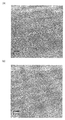
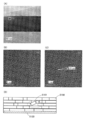
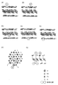
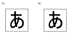
- FIG. 6A and 6B illustrate a cross-sectional TEM image of an oxide semiconductor film.
- 10A and 10B each illustrate a cross-sectional TEM image in which auxiliary lines are drawn from the cross-sectional TEM image of an oxide semiconductor film.
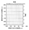
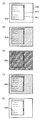
- FIG. 6 illustrates a cross-sectional TEM image obtained by performing image processing on a cross-sectional TEM image of an oxide semiconductor film. The figure explaining a measurement coordinate. The figure explaining a XRD result.
- FIG. 10 is a cross-sectional view illustrating a transistor.
- 4A and 4B illustrate a CV characteristic of a transistor.
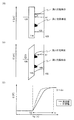
- 5A and 5B illustrate a band structure of an oxide semiconductor film and a diagram illustrating CV characteristics of a transistor.
- 4A and 4B illustrate a CV characteristic of a transistor.
- FIG. 4A and 4B are a top view and cross-sectional views illustrating a transistor.
- 4A and 4B illustrate a CV characteristic of a transistor.
- 4A and 4B illustrate a CV characteristic of a transistor.
- 10A and 10B each illustrate an in-plane distribution of field effect mobility of a transistor.
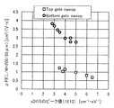
- 6A and 6B illustrate a relationship between a shallow defect state density and a field effect mobility of a transistor.
- FIG. 6 is a Cs-corrected high-resolution TEM image in a cross section of a CAAC-OS and a schematic cross-sectional view of the CAAC-OS.
- FIG. 6A and 6B illustrate structural analysis by XRD of a CAAC-OS and a single crystal oxide semiconductor.
- FIG. 6 shows changes in crystal parts of an In—Ga—Zn oxide due to electron irradiation.
- 8A and 8B illustrate a method for forming a CAAC-OS.
- FIG. 6 illustrates a crystal of InMZnO 4 .
- 8A and 8B illustrate a method for forming a CAAC-OS.
- 8A and 8B are a top view and a cross-sectional view illustrating an example of a semiconductor device.
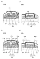
- FIG. 14 is a cross-sectional view illustrating an example of a semiconductor device. The figure explaining a band structure.
- FIG. 14 is a cross-sectional view illustrating an example of a semiconductor device.
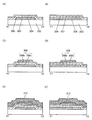
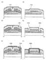
- 9 is a cross-sectional view illustrating an example of a manufacturing process of a semiconductor device.
- 9 is a cross-sectional view illustrating an example of a manufacturing process of a semiconductor device.
- FIG. 9 is a cross-sectional view illustrating an example of a manufacturing process of a semiconductor device.
- FIG. 9 is a model diagram illustrating oxygen moving into an oxide semiconductor film.
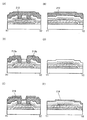
- 9 is a cross-sectional view illustrating an example of a manufacturing process of a semiconductor device.
- 9 is a cross-sectional view illustrating an example of a manufacturing process of a semiconductor device.
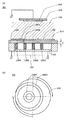
- FIG. 9 illustrates a sputtering apparatus.
- FIG. 9 illustrates a sputtering apparatus.
- FIG. 9 illustrates a sputtering apparatus.
- FIG. 9 illustrates a sputtering apparatus.
- FIG. 9 illustrates a sputtering apparatus.
- FIG. 9 illustrates a sputtering apparatus.
- the top view which shows an example of the film-forming apparatus.
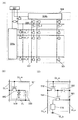
- FIG. 10 is a block diagram and a circuit diagram illustrating a display device.
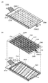
- the perspective view which shows an example of a touch panel.
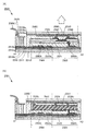
- Sectional drawing which shows an example of a display apparatus.
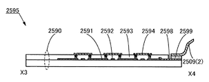
- Sectional drawing which shows an example of a touch sensor.
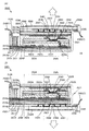
- Sectional drawing which shows an example of a touch panel.
- the circuit diagram of a touch sensor. 4A and 4B each illustrate display on a display device according to one embodiment of the present invention.
- 4A and 4B each illustrate display on a display device according to one embodiment of the present invention.
- 10A and 10B each illustrate an example of a display method on a display device according to Embodiment; 10A and 10B each illustrate an example of a display method on a display device according to Embodiment; The figure explaining a display module. 10A and 10B each illustrate an electronic device.
- FIG. 6 illustrates a structure of a film formation apparatus.
- the ordinal numbers attached as the first and second are used for convenience and do not indicate the order of steps or the order of lamination. Therefore, for example, the description can be made by appropriately replacing “first” with “second” or “third”.
- the ordinal numbers described in this specification and the like may not match the ordinal numbers used to specify one embodiment of the present invention.
- a semiconductor device refers to all devices that can function by utilizing semiconductor characteristics.
- a semiconductor element such as a transistor, a semiconductor circuit, an arithmetic device, and a memory device are one embodiment of the semiconductor device.
- An imaging device, a display device, a liquid crystal display device, a light emitting device, an electro-optical device, a power generation device (including a thin film solar cell, an organic thin film solar cell, and the like) and an electronic device may include a semiconductor device.
- the “semiconductor” in this specification and the like can be called an “insulator” in some cases.
- an “insulator” in this specification and the like can be called a “semiconductor” in some cases.
- the “insulator” in this specification and the like can be referred to as a “semi-insulator” in some cases.
- the semiconductor device may have characteristics as a “conductor”. Further, the boundary between the “semiconductor” and the “conductor” is ambiguous, and there are cases where it cannot be strictly distinguished. Therefore, a “semiconductor” in this specification and the like can be called a “conductor” in some cases. Similarly, a “conductor” in this specification and the like can be called a “semiconductor” in some cases.
- a transistor is an element having at least three terminals including a gate, a drain, and a source.
- a channel region is provided between the drain (drain terminal, drain region or drain electrode) and the source (source terminal, source region or source electrode), and a current flows through the drain, channel region, and source. It is something that can be done.
- a channel region refers to a region through which a current mainly flows.
- the functions of the source and drain may be switched when transistors with different polarities are used or when the direction of current changes during circuit operation. Therefore, in this specification and the like, the terms source and drain can be used interchangeably.
- the channel length refers to, for example, a region where a semiconductor (or a portion where current flows in the semiconductor when the transistor is on) and a gate electrode overlap with each other in a top view of the transistor, or a region where a channel is formed
- the channel length is not necessarily the same in all regions. That is, the channel length of one transistor may not be fixed to one value. Therefore, in this specification and the like, the channel length is any one of values, the maximum value, the minimum value, or the average value in a region where a channel is formed.
- the channel width is, for example, a region in which a semiconductor (or a portion in which a current flows in the semiconductor when the transistor is on) and a gate electrode overlap each other, or a source and a drain in a region where a channel is formed. This is the length of the part. Note that in one transistor, the channel width is not necessarily the same in all regions. That is, the channel width of one transistor may not be fixed to one value. Therefore, in this specification and the like, the channel width is any one of values, the maximum value, the minimum value, or the average value in a region where a channel is formed.
- “electrically connected” includes a case of being connected via “something having an electric action”.
- the “thing having some electric action” is not particularly limited as long as it can exchange electric signals between connection targets.
- “thing having some electric action” includes electrodes, wiring, switching elements such as transistors, resistance elements, inductors, capacitors, and other elements having various functions.
- the voltage often indicates a potential difference between a certain potential and a reference potential (for example, a ground potential (GND) or a source potential). Therefore, a voltage can be rephrased as a potential.
- a reference potential for example, a ground potential (GND) or a source potential. Therefore, a voltage can be rephrased as a potential.
- a silicon oxynitride film refers to a film having a higher oxygen content than nitrogen, preferably 55 to 65 atomic% oxygen and 1 atomic% nitrogen. More than 20 atomic%, silicon is included in a range of 25 atomic% to 35 atomic%, and hydrogen is included in a range of 0.1 atomic% to 10 atomic%.
- the silicon nitride oxide film refers to a film having a nitrogen content higher than that of oxygen as a composition.
- nitrogen is 55 atomic% to 65 atomic%
- oxygen is 1 atomic% to 20 atomic%
- silicon is included. This refers to a concentration range of 25 atomic% to 35 atomic% and hydrogen in a concentration range of 0.1 atomic% to 10 atomic%.
- film and “layer” can be interchanged.
- conductive layer may be changed to the term “conductive film”.
- insulating film may be changed to the term “insulating layer” in some cases.
- parallel means a state in which two straight lines are arranged at an angle of ⁇ 10 ° to 10 °. Therefore, the case of ⁇ 5 ° to 5 ° is also included.
- substantially parallel means a state in which two straight lines are arranged at an angle of ⁇ 30 ° to 30 °.
- Vertical refers to a state in which two straight lines are arranged at an angle of 80 ° to 100 °. Therefore, the case of 85 ° to 95 ° is also included.
- substantially vertical means a state in which two straight lines are arranged at an angle of 60 ° to 120 °.
- semiconductor impurities refer to components other than the main components constituting the semiconductor.
- an element having a concentration of less than 0.1 atomic% is an impurity.
- DOS Density of State
- examples of impurities that change the characteristics of the semiconductor include Group 1 elements, Group 2 elements, Group 14 elements, Group 15 elements, and transition metals other than the main component.
- oxygen vacancies may be formed by mixing impurities such as hydrogen, for example.
- examples of impurities that change the characteristics of the semiconductor include Group 1 elements, Group 2 elements, Group 13 elements, and Group 15 elements other than oxygen and hydrogen.
- the oxide semiconductor film of one embodiment of the present invention includes indium (In), M (M represents Al, Ga, Y, or Sn), and zinc (Zn).
- the oxide semiconductor film contains In, for example, carrier mobility (electron mobility) increases.
- the oxide semiconductor film includes the element M for example, the energy gap (Eg) of the oxide semiconductor film is increased.
- the element M is an element having a high binding energy with oxygen, and the binding energy with oxygen is higher than that of In.
- the oxide semiconductor film contains Zn the oxide semiconductor film is likely to be crystallized.
- an In—Ga oxide, an In—Zn oxide, or an In—M—Zn oxide can be used as the oxide semiconductor film of one embodiment of the present invention.
- an In—Ga—Zn oxide (hereinafter sometimes referred to as IGZO) in which M is Ga is preferably used.
- the oxide semiconductor film is an In-M-Zn oxide
- the atomic ratio of the metal elements of the sputtering target used for forming the In-M-Zn oxide satisfies In ⁇ M and Zn ⁇ M. It is preferable to satisfy.
- the atomic ratio of the oxide semiconductor film to be formed includes a variation of plus or minus 40% of the atomic ratio of the metal element contained in the sputtering target as an error.
- the oxide semiconductor film has an energy gap of 2 eV or more, preferably 2.5 eV or more, more preferably 3 eV or more.
- impurities such as hydrogen or moisture mixed in the oxide semiconductor film in the channel region are problematic because they affect the transistor characteristics. Accordingly, it is preferable that impurities such as hydrogen or moisture be smaller in the channel region of the oxide semiconductor film.
- oxygen vacancies formed in the oxide semiconductor film in the channel region are problematic because they affect transistor characteristics. For example, when an oxygen vacancy is formed in the oxide semiconductor film in the channel region, hydrogen is bonded to the oxygen vacancy to serve as a carrier supply source. When a carrier supply source is generated in the oxide semiconductor film in the channel region, a change in electrical characteristics of the transistor including the oxide semiconductor film, typically, a threshold voltage shift occurs. In addition, there is a problem that electric characteristics vary from transistor to transistor. Therefore, the number of oxygen vacancies is preferably as small as possible in the channel region of the oxide semiconductor film.
- the transistor including the oxide semiconductor film causes deterioration and the like. Therefore, in order to impart stable electrical characteristics to the transistor including an oxide semiconductor film, it is important to reduce the defect level or the defect level density in the oxide semiconductor film and in the vicinity of the interface thereof.
- the defect levels include a defect level at a shallow position and a defect level at a deep position.
- a defect level at a shallow position refers to a defect level between the energy (Ec) at the lower end of the conduction band and a mid gap. Therefore, for example, the defect level at the shallow position is located near the energy at the lower end of the conduction band.
- the defect level at a deep position refers to a defect level between the energy (Ev) at the top of the valence band and the mid gap. Therefore, for example, the defect level at a deep position is located closer to the mid gap than the energy at the top of the valence band.
- the field-effect mobility (also referred to simply as mobility, ⁇ FE) of a transistor including an oxide semiconductor film is achieved by reducing the shallow defect level or the density of shallow defect states at the interface between the oxide semiconductor film and the outside. ) Can be increased. Alternatively, variation in electrical characteristics of a transistor including an oxide semiconductor film can be reduced.
- At least one or more of impurities typically hydrogen or moisture
- oxygen vacancies, and defect level density in an oxide semiconductor film is reduced.
- impurities typically hydrogen or moisture
- oxygen vacancies, and defect level density in an oxide semiconductor film is reduced.
- An oxide semiconductor is classified into a single crystal oxide semiconductor and a non-single-crystal oxide semiconductor.
- a CAAC-OS C Axis Crystalline Oxide Semiconductor
- a polycrystalline oxide semiconductor an nc-OS (Nanocrystalline Semiconductor)
- a pseudo-amorphous oxide semiconductor a-liquid oxide OS like Oxide Semiconductor
- amorphous oxide semiconductor a-liquid oxide OS
- oxide semiconductors are classified into non-quality oxide semiconductors and other crystalline oxide semiconductors.
- a crystalline oxide semiconductor include a single crystal oxide semiconductor, a CAAC-OS, a polycrystalline oxide semiconductor, and an nc-OS.
- the amorphous structure As the definition of the amorphous structure, it is generally known that it is not fixed in a metastable state, isotropic and does not have a heterogeneous structure. Moreover, it can be paraphrased as a structure having a flexible bond angle and short-range order, but not long-range order.
- an oxide semiconductor that is not isotropic eg. has a periodic structure in a minute region
- an oxide semiconductor that is not isotropic eg. has a periodic structure in a minute region
- the a-like OS has a periodic structure in a minute region
- it has a void also referred to as a “hode”
- is an unstable structure therefore, it can be said that it is close to an amorphous oxide semiconductor in terms of physical properties.
- CAAC-OS is particularly preferable among the above oxide semiconductors.
- the oxide semiconductor film is a CAAC-OS, the crystallinity of the oxide semiconductor film can be increased and the density of impurities, oxygen vacancies, or defect states in the oxide semiconductor film can be reduced.
- the details of the above-described CAAC-OS, nc-OS, a-like OS, and the like will be described later.
- Crystallinity of oxide semiconductor film As for the crystallinity of the oxide semiconductor film, an analysis of a cross section of the oxide semiconductor film using a transmission electron microscope (TEM) and an X-ray diffraction (XRD) of the oxide semiconductor film is performed. It can be evaluated by performing analysis. Below, the oxide semiconductor film for TEM analysis and the oxide semiconductor film for XRD analysis were produced, and the crystallinity of the oxide semiconductor film was evaluated.
- TEM transmission electron microscope
- XRD X-ray diffraction
- FIG. 4 the coordinates of a 720 mm ⁇ 600 mm glass substrate when the TEM analysis is performed are shown in FIG.
- one side of the substrate is divided into six regions with respect to the 720 mm direction, which are region 1 to region 6, respectively.
- one side of the substrate is divided into 15 regions with respect to the direction of 600 mm, which are referred to as regions A to O, respectively.
- the distance from the center of the substrate is within a range of ⁇ 20 mm to 20 mm when the one side of the substrate is in the 600 mm direction, and the distance from the center of the substrate is one in the 720 mm direction
- the vicinity of the center of the substrate within the range is referred to as a region H3.
- the coordinates of the TEM analysis were the area B3 and the area H3 shown in FIG.
- the region B3 may be referred to as a substrate outer periphery
- the region H3 may be referred to as a substrate center.
- the TEM analysis was performed using an atomic resolution analytical electron microscope JEM-ARM200F manufactured by JEOL Ltd.
- the measurement conditions were an acceleration voltage of 200 kV and a magnification of 4 million times.
- FIGS. 1A and 1B show cross-sectional TEM images of the oxide semiconductor film.
- 1A is a cross-sectional TEM image of the substrate center (region H3)
- FIG. 1B is a cross-sectional TEM image of the substrate outer periphery (region B3).
- the oxide semiconductor film of one embodiment of the present invention has a cross-sectional TEM image in which atoms can be confirmed when a cross-sectional TEM analysis is performed.
- a region having c-axis orientation (hereinafter also referred to as a first region) is included.
- FIGS. 1A and 1B the region having the c-axis orientation (first region) may not be clearly identified, and thus an auxiliary line is added to the cross-sectional TEM images in FIGS.
- subjected is shown to FIG. 2 (A) (B).
- 2A is a cross-sectional TEM image with white lines added as auxiliary lines in FIG. 1A
- FIG. 2B is a cross-sectional TEM image with white lines added as auxiliary lines in FIG. 1B.
- the white auxiliary lines shown in FIGS. 2A and 2B are drawn with respect to the lattice stripes in the region (first region) having c-axis orientation.
- the oxide semiconductor film of one embodiment of the present invention has c-axis alignment in one field of a cross-sectional TEM image in which atoms can be confirmed when cross-sectional TEM analysis is performed.
- a region (first region) and a region having no orientation on the c-axis (hereinafter also referred to as a second region).
- the first region can be rephrased as a region in which the c-axis is oriented in a direction parallel to the normal vector of the upper surface of the film.
- the second region can also be referred to as a region having no orientation or a region in which orientation to the c-axis is difficult to be observed.
- the second region may be referred to as an atomic void.
- the oxide semiconductor film in the center of the substrate (region H3) shown in A) has a larger proportion of the region having the c-axis orientation (first region).
- the area of the region having the c-axis orientation (first region and the region having no c-axis orientation (second region) of the oxide semiconductor film illustrated in FIGS. Image calculation was performed, and the ratio between the region having the c-axis orientation (first region) and the region having no orientation on the c-axis (second region) was calculated.
- FIGS. 3A and 3B are results of image analysis of the cross-sectional TEM images of the oxide semiconductor film illustrated in FIGS.
- FIG. 3A shows the image analysis result of FIG. 2A
- FIG. 3B shows the image analysis result of FIG. 2B.
- the quantified range was the range of the region 10 shown in FIGS. 3A and 3B (here, one area of the cross-sectional TEM image was approximately 30 nm 2 ).
- the range of the region 10 subjected to quantification is not limited thereto, and for example, the area of the cross-sectional TEM image is in the range of 5 nm 2 to 500 nm 2 , preferably in the range of 5 nm 2 to 100 nm 2 , more preferably. May be performed in the range of 5 nm 2 to 50 nm 2 .
- the white filled region 11 is a region (first region) having c-axis orientation, and the gray filled region 12 has orientation on the c-axis. There is no region (second region).
- the area of the first region in FIG. 3A is 76.7%, and the area of the second region is 23.3. %Met.
- the area of the first region in FIG. 3B was 52.8%, and the area of the second region was 47.2%.
- a region different from a region having a c-axis orientation in other words, a region having no orientation in the c-axis (second region)
- first region a region having a c-axis orientation
- second region a region having no orientation in the c-axis
- an oxide semiconductor film for XRD analysis is described.
- an oxide semiconductor film for XRD analysis an oxide semiconductor film having a thickness of 100 nm was formed over a glass substrate having a size of 720 mm ⁇ 600 mm. Note that the oxide semiconductor film was formed by a sputtering method.
- XRD analysis was performed using a multifunctional thin film material evaluation X-ray diffractometer D8 DISCOVER Hybrid (manufactured by Bruker AXS). Moreover, as the XRD analysis, the out-of-plane method was used.
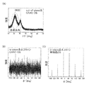
- 5A and 5B show the XRD analysis results of the oxide semiconductor film.
- 5A shows the XRD result of the substrate center (region H3)
- FIG. 5B shows the XRD result of the substrate outer periphery (region B3).
- the defect level density can be evaluated, for example, by comparing the measured value of the high-frequency CV characteristic of the transistor with the calculated value of the CV characteristic.
- FIG. 6 is a schematic cross-sectional view of the transistor used in the calculation. 6 includes the insulating film 103, the oxide semiconductor film 108, the conductive films 112 a and 112 b, the insulating film 116, and the conductive film 120.
- the oxide semiconductor film 108 has a region overlapping with the conductive film 120 with the insulating film 116 interposed therebetween.
- the conductive film 120 functions as a gate electrode.
- the insulating film 116 functions as a gate insulating film.
- the conductive films 112a and 112b are in contact with the oxide semiconductor film 108 and function as a source electrode and a drain electrode. Note that a transistor actually manufactured and used for measurement also has a similar cross-sectional structure.
- the donor density of the oxide semiconductor film 108 in the region where the conductive films 112a and 112b are in contact with the oxide semiconductor film 108 was 1 ⁇ 10 19 cm ⁇ 3 .
- FIG. 7A shows an ideal CV characteristic obtained by calculation and a result of the CV characteristic measured by fabricating a transistor.
- an In—Ga—Zn oxide having physical properties shown in Table 1 was used as the oxide semiconductor film 108.
- the CV characteristics are measured by applying a voltage (gate voltage Vg) between the conductive films 112a and 112b and the conductive film 120 from -10V to 10V at intervals of 0.1V, and then 10V. To -10V at 0.1V intervals.
- Vg a voltage between the conductive films 112a and 112b and the conductive film 120 from -10V to 10V at intervals of 0.1V, and then 10V.
- As the gate voltage Vg 1 kHz AC voltage and DC voltage were applied.
- the capacitance may be measured to be smaller as the frequency of the AC voltage is higher.
- the frequency of the AC voltage may be selected as appropriate in accordance with the channel length of the transistor.
- the frequency of the AC voltage in the channel length of a practical transistor includes, for example, 0.1 kHz to 10 MHz, 0.2 kHz to 1 MHz, 0.3 kHz to 100 kHz, or 0.3 kHz to 10 kHz.
- a method for evaluating a shallow defect level density will be described using the schematic CV characteristics shown in FIG.
- a change in the gate voltage Vg when the capacitance changes from C1 to C2 is defined as ⁇ V id .
- ⁇ V ex is a change in the gate voltage Vg when the capacitance changes from C1 to C2.
- the amount of change in potential at the interface between the oxide semiconductor film 108 and the insulating film 116 when the capacitance changes from C1 to C2 is denoted by ⁇ .
- ⁇ V id is always smaller than ⁇ V ex because the measured value has a slower slope of the CV characteristic than the calculated value.
- the difference between ⁇ V ex and ⁇ V id represents the potential difference required to trap electrons in the shallow defect level. Therefore, when the amount of change in charge due to electrons trapped at the interface between the oxide semiconductor film 108 and the insulating film 116 is ⁇ Q SS and the capacitance of the insulating film 116 is C OX , ⁇ Q SS is expressed by the following equation (1). Is done.
- Equation (2) N SS is the shallow defect level density per unit area and energy at the interface, and A is the area of the channel region of the transistor. Note that q is an elementary electric quantity.
- Formula (3) can be obtained by combining Formula (1) and Formula (2).
- formula (4) can be obtained by taking the limit of formula (3).
- the measured value and the calculated value can be fitted by setting N to 2.9 ⁇ 10 13 cm ⁇ 2 eV ⁇ 1 and W to 0.10 eV. That is, the peak value N of the shallow defect level density can be derived as 2.9 ⁇ 10 13 cm ⁇ 2 eV ⁇ 1 . Further, from the integrated value of the curve fitted with Gaussian, 5.1 ⁇ 10 12 cm ⁇ 2 is obtained as the shallow defect level density N SS .
- FIG. 7B shows a comparison between the results of calculating the CV characteristics and the measured values of the CV characteristics using the Gaussian-type shallow defect level density expressed by Equation (5). Show. As a result, it can be seen that the calculated value and the measured value of the CV characteristic have high reproducibility. Therefore, it can be seen that the above method is sufficiently appropriate as a method for calculating the shallow defect level density.
- the defect level density in the oxide semiconductor film is obtained by using the evaluation method described in ⁇ 1-4 Evaluation method of defect level density>. Was measured.
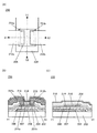
- FIGS. 10A is a top view of the transistor 600
- FIG. 10B corresponds to a cross-sectional view of a cross section taken along dashed-dotted line A1-A2 in FIG. 10A.
- the transistor 600 includes a conductive film 604 functioning as a first gate electrode over the substrate 602, an insulating film 606 over the substrate 602 and the conductive film 604, an insulating film 607 over the insulating film 606, and an oxide film over the insulating film 607.
- insulating films 614, 616, and 618 are provided over the transistor 600, more specifically, over the conductive films 612 a and 612 b and the oxide semiconductor film 608.
- a conductive film 620 is provided over the insulating film 618. Note that the insulating films 606 and 607 function as a first gate insulating film.
- the insulating films 614, 616, and 618 function as a second gate insulating film.
- the conductive film 620 functions as a second gate electrode (also referred to as a back gate electrode) of the transistor 600.
- insulating films 606 and 607 were formed over the substrate 602 and the conductive film 604.
- a silicon nitride film having a thickness of 400 nm was formed using a PECVD apparatus.
- insulating film 607 a 50-nm-thick silicon oxynitride film was formed using a PECVD apparatus.
- an oxide semiconductor film 608 was formed over the insulating film 607.
- an IGZO film having a thickness of 35 nm was formed using a sputtering apparatus and then processed into a desired shape.
- the first heat treatment was performed.
- heat treatment was performed at 450 ° C. for 1 hour in a nitrogen atmosphere, and subsequently, heat treatment was performed at 450 ° C. for 1 hour in a mixed gas atmosphere of nitrogen and oxygen.
- a conductive film was formed over the insulating film 607 and the oxide semiconductor film 608, a resist mask was formed over the conductive film, and desired regions were etched to form conductive films 612a and 612b.
- a 50-nm-thick tungsten film, a 400-nm-thick aluminum film, and a 100-nm-thick titanium film were successively formed in a vacuum using a sputtering apparatus. Note that the resist mask was removed after the formation of the conductive films 612a and 612b.
- a phosphoric acid aqueous solution (an aqueous solution in which an aqueous solution having a phosphoric acid concentration of 85% is further diluted 100 times with pure water) is applied over the insulating film 607, the oxide semiconductor film 608, and the conductive films 612a and 612b. Then, part of the surface of the oxide semiconductor film 608 exposed from the conductive films 612a and 612b was removed.
- the insulating film 614 and the insulating film 616 were formed over the insulating film 607, the oxide semiconductor film 608, and the conductive films 612a and 612b.
- a 50-nm-thick silicon oxynitride film was formed using a PECVD apparatus.
- As the insulating film 616 a 400-nm-thick silicon oxynitride film was formed using a PECVD apparatus. Note that the insulating film 614 and the insulating film 616 were continuously formed in a vacuum using a PECVD apparatus.
- the substrate temperature was set to 220 ° C.
- a silane gas having a flow rate of 50 sccm, and nitrous oxide gas having a flow rate of 2000 sccm were introduced into the chamber
- the pressure was set to 20 Pa
- the PECVD apparatus was installed.
- a film was formed by supplying RF power of 100 W between parallel plate electrodes.
- the insulating film 616 is formed by setting the substrate temperature to 220 ° C., introducing silane gas having a flow rate of 160 sccm and dinitrogen monoxide gas having a flow rate of 4000 sccm into the chamber, setting the pressure to 200 Pa, and installing it in the PECVD apparatus.
- the film was formed by supplying 1500 W of RF power between the parallel plate electrodes.
- the second heat treatment was performed at 350 ° C. for 1 hour in an atmosphere containing nitrogen.
- oxygen addition treatment was performed on the insulating films 614 and 616.
- an ashing device is used, a substrate temperature is set to 40 ° C., an oxygen gas having a flow rate of 250 sccm is introduced into the chamber, a pressure is set to 15 Pa, and a bias is applied to the substrate side. 4500 W of RF power was supplied between the electrodes of the parallel plates installed in the plate.
- an insulating film 618 was formed over the insulating film 616.
- a silicon nitride film with a thickness of 100 nm was formed using a PECVD apparatus.
- the conditions for forming the insulating film 618 are as follows: the substrate temperature is set to 350 ° C., a silane gas having a flow rate of 50 sccm, a nitrogen gas having a flow rate of 5000 sccm, and an ammonia gas having a flow rate of 100 sccm are introduced into the chamber.
- the film was formed by supplying RF power of 1000 W between the electrodes of the parallel plates installed in the plate.
- a conductive film was formed over the insulating film 618, and the conductive film was processed to form a conductive film 620.
- an ITSO film with a thickness of 100 nm was formed using a sputtering apparatus.
- the third heat treatment was performed at 250 ° C. for 1 hour in a nitrogen atmosphere.
- the transistor for CV characteristic evaluation was produced by the above process. Note that the transistor has a channel length L of 200 ⁇ m and a channel width W of 50 ⁇ m.
- a voltage (also referred to as a gate voltage Vg) between the conductive films 612a and 612b and the conductive film 604 or the conductive film 620 was applied at intervals of 0.2V from -10V to 10V.
- a gate voltage Vg an AC voltage of 10 kHz was applied.
- 11A and 11B show measurement results of the CV characteristics of the manufactured transistor.
- the coordinates of the 720 mm ⁇ 600 mm size glass substrate of the transistor whose CV characteristics were measured were the vicinity of the substrate center (region 13 and region J3) and the vicinity of the substrate periphery (region L3 and region N3).
- the coordinate of the glass substrate of a 720 mm x 600 mm size shown in FIG. 4 is used as a coordinate of a glass substrate.
- FIG. 11A shows the result of Top Gate Sweep
- FIG. 11B shows the result of Bottom Gate Sweep. 11A and 11B
- the vertical axis represents the capacitance C
- the horizontal axis represents the gate voltage Vg.
- the capacity of Top Gate Sweep was smaller than that of Bottom Gate Sweep.
- the change in capacitance with respect to the gate voltage Vg was smaller in the vicinity of the substrate periphery than in the vicinity of the substrate center.
- defect level density was calculated by comparing the measured value of the CV characteristic with the calculated value of the CV characteristic.
- ⁇ 1-4 The description of evaluation method of defect level density> may be referred to.
- FIG. 12 shows a result obtained by fitting a Gaussian curve (calculated value) represented by the above-described equation (5) to the CV characteristic measured by Bottom Gate Sweep in the vicinity of the center of the substrate of the transistor (region 13). Shown in (A).
- the calculated value of the measured value and the C-V characteristics of the C-V characteristic and from that roughly coincides with the fitting, to calculate a shallow defect level density N SS in the oxide semiconductor film 608 You can see that In FIG. 12A, by setting N to 2.8 ⁇ 10 12 cm ⁇ 2 eV ⁇ 1 and W to 0.07 eV, the measured value and the calculated value of the CV characteristic can be fitted. did it. That is, the peak value N of the shallow defect level density could be derived as 2.8 ⁇ 10 12 cm ⁇ 2 eV ⁇ 1 . Note that a shallow defect state density NSS is obtained from the integral value of the curve.
- sDOS tends to increase from the vicinity of the center of the substrate toward the vicinity of the outer periphery of the substrate. This tendency was suggested to be inversely correlated with the height of crystallinity from the cross-sectional TEM image described above or the size of the peak due to the spinel crystal structure obtained by XRD.
- an oxide semiconductor film with high crystallinity can be said to be an oxide semiconductor film with a small peak value of sDOS.
- transistor characteristics are field-effect mobility ( ⁇ FE) obtained from the Id-Vg characteristics.
- ⁇ FE field-effect mobility
- the coordinates of the glass substrate on which the field effect mobility ( ⁇ FE) was measured were region C3, region D3, region F3, region G3, region I3, region J3, region L3, and region M3.
- a coordinate of a glass substrate the coordinate of the glass substrate of a 720 mm x 600 mm size shown in FIG. 4 is used.
- FIG. 14 shows the relationship between the field effect mobility ( ⁇ FE) obtained from the Id-Vg characteristics of the transistor and the distance from the center of the substrate.
- the field effect mobility ( ⁇ FE) tends to decrease from the vicinity of the center of the substrate to the vicinity of the outer periphery of the substrate.
- FIG. 15 is a diagram for explaining the correlation between the result of the peak value of sDOS and the field effect mobility.
- the vertical axis represents field effect mobility ( ⁇ FE)
- the horizontal axis represents the peak value of sDOS.
- the field effect mobility of the transistor tends to increase as the peak value of sDOS decreases.
- the peak value of sDOS is less than 1 ⁇ 10 13 cm ⁇ 2 eV ⁇ 1 , more preferably less than 2 ⁇ 10 12 cm ⁇ 2 eV ⁇ 1 , and even more preferably less than 1 ⁇ 10 10 cm ⁇ 2 eV ⁇ 1 .
- a transistor including the oxide semiconductor film has high field-effect mobility.
- Embodiment 2 In this embodiment, the details of the oxide semiconductor described in Embodiment 1 will be described with reference to FIGS.
- CAAC-OS First, the CAAC-OS will be described.
- CAAC-OS is one of oxide semiconductors having a plurality of c-axis aligned crystal parts (also referred to as pellets).
- a composite analysis image also referred to as a high-resolution TEM image
- a diffraction pattern of CAAC-OS is observed with a TEM
- a plurality of pellets can be confirmed.
- the boundary between pellets that is, the crystal grain boundary (also referred to as grain boundary) cannot be clearly confirmed. Therefore, it can be said that the CAAC-OS does not easily lower the electron mobility due to the crystal grain boundary.
- FIG. 16A illustrates a high-resolution TEM image of a cross section of the CAAC-OS which is observed from a direction substantially parallel to the sample surface.
- a spherical aberration correction function was used for observation of the high-resolution TEM image.
- a high-resolution TEM image using the spherical aberration correction function is particularly referred to as a Cs-corrected high-resolution TEM image.
- Acquisition of a Cs-corrected high-resolution TEM image can be performed by, for example, an atomic resolution analytical electron microscope JEM-ARM200F manufactured by JEOL Ltd.
- FIG. 16B shows a Cs-corrected high-resolution TEM image obtained by enlarging the region (1) in FIG. FIG. 16B shows that metal atoms are arranged in a layered manner in a pellet.
- the arrangement of each layer of metal atoms reflects unevenness on a surface (also referred to as a formation surface) or an upper surface where a CAAC-OS film is formed, and is parallel to the formation surface or upper surface of the CAAC-OS.
- the CAAC-OS has a characteristic atomic arrangement.
- FIG. 16C shows a characteristic atomic arrangement with auxiliary lines. From FIG. 16B and FIG. 16C, it can be seen that the size of one pellet is about 1 nm to 3 nm, and the size of the gap caused by the inclination between the pellet and the pellet is about 0.8 nm. Therefore, the pellet can also be referred to as a nanocrystal (nc).
- the CAAC-OS can also be referred to as an oxide semiconductor including CANC (C-Axis aligned nanocrystals).
- FIG. 17A shows a Cs-corrected high-resolution TEM image of the plane of the CAAC-OS observed from a direction substantially perpendicular to the sample surface.
- the Cs-corrected high-resolution TEM images obtained by enlarging the region (1), the region (2), and the region (3) in FIG. 17A are shown in FIGS. 17B, 17C, and 17D, respectively. Show. From FIG. 17B, FIG. 17C, and FIG. 17D, it can be confirmed that the metal atoms are arranged in a triangular shape, a square shape, or a hexagonal shape in the pellet. However, there is no regularity in the arrangement of metal atoms between different pellets.
- CAAC-OS analyzed by XRD will be described.
- a peak appears when the diffraction angle (2 ⁇ ) is around 31 ° as illustrated in FIG. There is. Since this peak is attributed to the (009) plane of the InGaZnO 4 crystal, the CAAC-OS crystal has c-axis orientation, and the c-axis is oriented in a direction substantially perpendicular to the formation surface or the top surface. It can be confirmed.
- a peak at 2 ⁇ of around 36 ° may appear in structural analysis by the out-of-plane method of the CAAC-OS.
- a peak at 2 ⁇ of around 36 ° indicates that a crystal having no c-axis alignment is included in part of the CAAC-OS.
- 2 ⁇ has a peak in the vicinity of 31 °, and 2 ⁇ has no peak in the vicinity of 36 °.
- a CAAC-OS analyzed by electron diffraction will be described.
- a diffraction pattern (a limited-field transmission electron diffraction pattern as shown in FIG. 19A) is obtained. Say) may appear.
- This diffraction pattern includes spots caused by the (009) plane of the InGaZnO 4 crystal. Therefore, electron diffraction shows that the pellets included in the CAAC-OS have c-axis alignment, and the c-axis is in a direction substantially perpendicular to the formation surface or the top surface.
- FIG. 19B shows a diffraction pattern obtained when an electron beam with a probe diameter of 300 nm is incident on the same sample in a direction perpendicular to the sample surface. From FIG. 19B, a ring-shaped diffraction pattern is confirmed. Therefore, electron diffraction shows that the a-axis and the b-axis of the pellet included in the CAAC-OS have no orientation. Note that the first ring in FIG. 19B is considered to originate from the (010) plane and the (100) plane of the InGaZnO 4 crystal. Further, the second ring in FIG. 19B is considered to be due to the (110) plane and the like.
- the CAAC-OS is an oxide semiconductor with high crystallinity. Since the crystallinity of an oxide semiconductor may be deteriorated by entry of impurities, generation of defects, or the like, in reverse, the CAAC-OS can be said to be an oxide semiconductor with few impurities and defects (such as oxygen vacancies).
- the impurity means an element other than the main components of the oxide semiconductor, such as hydrogen, carbon, silicon, or a transition metal element.
- an element such as silicon which has a stronger bonding force with oxygen than a metal element included in an oxide semiconductor, disturbs the atomic arrangement of the oxide semiconductor by depriving the oxide semiconductor of oxygen, thereby reducing crystallinity. It becomes a factor.
- heavy metals such as iron and nickel, argon, carbon dioxide, and the like have large atomic radii (or molecular radii), which disturbs the atomic arrangement of the oxide semiconductor and decreases crystallinity.
- an impurity contained in the oxide semiconductor might serve as a carrier trap or a carrier generation source.
- oxygen vacancies in the oxide semiconductor may serve as carrier traps or may serve as carrier generation sources by capturing hydrogen.
- a CAAC-OS with few impurities and oxygen vacancies is an oxide semiconductor with low carrier density.
- the carrier density is less than 8 ⁇ 10 11 / cm 3 , preferably less than 1 ⁇ 10 11 / cm 3 , more preferably less than 1 ⁇ 10 10 / cm 3 , and 1 ⁇ 10 ⁇ 9 / cm 3. This can be done.
- Such an oxide semiconductor is referred to as a highly purified intrinsic or substantially highly purified intrinsic oxide semiconductor.
- the CAAC-OS has a low impurity concentration and a low density of defect states. That is, it can be said that the oxide semiconductor has stable characteristics.
- the nc-OS has a region where a crystal part can be confirmed and a region where a clear crystal part cannot be confirmed in a high-resolution TEM image.
- a crystal part included in the nc-OS has a size of 1 nm to 10 nm, or 1 nm to 3 nm.
- an oxide semiconductor in which the size of a crystal part is greater than 10 nm and less than or equal to 100 nm is sometimes referred to as a microcrystalline oxide semiconductor.
- the nc-OS may not be able to clearly confirm a crystal grain boundary in a high-resolution TEM image.
- the nanocrystal may have the same origin as the pellet in the CAAC-OS. Therefore, the crystal part of nc-OS is sometimes referred to as a pellet below.
- Nc-OS has periodicity in atomic arrangement in a minute region (for example, a region of 1 nm to 10 nm, particularly a region of 1 nm to 3 nm).
- the nc-OS has no regularity in crystal orientation between different pellets. Therefore, orientation is not seen in the whole film. Therefore, the nc-OS may not be distinguished from an a-like OS or an amorphous oxide semiconductor depending on an analysis method. For example, when an X-ray having a diameter larger than that of the pellet is used for nc-OS, a peak indicating a crystal plane is not detected in the analysis by the out-of-plane method.
- a diffraction pattern such as a halo pattern is observed.
- nanobeam electron diffraction is performed on the nc-OS using an electron beam having a probe diameter that is close to the pellet size or smaller than the pellet size, spots are observed.
- a region with high luminance may be observed like a circle (in a ring shape).
- a plurality of spots may be observed in the ring-shaped region.
- nc-OS has an oxide semiconductor having RANC (Random Aligned nanocrystals), or NANC (Non-Aligned nanocrystals). It can also be called an oxide semiconductor.
- Nc-OS is an oxide semiconductor having higher regularity than an amorphous oxide semiconductor. Therefore, the nc-OS has a lower density of defect states than an a-like OS or an amorphous oxide semiconductor. Note that the nc-OS does not have regularity in crystal orientation between different pellets. Therefore, the nc-OS has a higher density of defect states than the CAAC-OS.
- the a-like OS is an oxide semiconductor having a structure between the nc-OS and an amorphous oxide semiconductor.
- a void may be observed in a high-resolution TEM image. Moreover, in a high-resolution TEM image, it has the area
- the a-like OS Since it has a void, the a-like OS has an unstable structure.
- the a-like OS has an unstable structure as compared with the CAAC-OS and the nc-OS, a change in structure due to electron irradiation is shown.
- sample A A-like OS (referred to as sample A), nc-OS (referred to as sample B), and CAAC-OS (referred to as sample C) are prepared as samples to be irradiated with electrons. Each sample is an In—Ga—Zn oxide.
- the determination of which part is regarded as one crystal part may be performed as follows.
- the unit cell of an InGaZnO 4 crystal has a structure in which three In—O layers and six Ga—Zn—O layers have a total of nine layers stacked in the c-axis direction.
- the spacing between these adjacent layers is about the same as the lattice spacing (also referred to as d value) of the (009) plane, and the value is determined to be 0.29 nm from crystal structure analysis. Therefore, a portion where the interval between lattice fringes is 0.28 nm or more and 0.30 nm or less can be regarded as a crystal part of InGaZnO 4 .
- the lattice fringes correspond to the ab plane of the InGaZnO 4 crystal.
- FIG. 20 shows an example in which the average size of the crystal parts (from 22 to 45) of each sample was examined.
- the length of the lattice fringes described above is the size of the crystal part.
- the crystal part becomes larger according to the cumulative dose of electrons.
- the crystal portion also referred to as initial nucleus
- the crystal portion which was about 1.2 nm in the initial stage of observation by TEM has a cumulative irradiation dose of 4.2. It can be seen that the film grows to a size of about 2.6 nm at ⁇ 10 8 e ⁇ / nm 2 .
- the crystal part sizes of the nc-OS and the CAAC-OS are about 1.4 nm, respectively, regardless of the cumulative electron dose. And about 2.1 nm.
- the crystal part may be grown by electron irradiation.
- the crystal part is hardly grown by electron irradiation. That is, it can be seen that the a-like OS has an unstable structure as compared with the nc-OS and the CAAC-OS.
- the a-like OS has a structure with a lower density than the nc-OS and the CAAC-OS. Specifically, the density of the a-like OS is 78.6% or more and less than 92.3% of the density of the single crystal having the same composition. Further, the density of the nc-OS and the density of the CAAC-OS are 92.3% or more and less than 100% of the density of the single crystal having the same composition. An oxide semiconductor that is less than 78% of the density of a single crystal is difficult to form.
- the density of single crystal InGaZnO 4 having a rhombohedral structure is 6.357 g / cm 3 .
- the density of a-like OS is 5.0 g / cm 3 or more and less than 5.9 g / cm 3.
- the density of the nc-OS and the density of the CAAC-OS is 5.9 g / cm 3 or more and 6.3 g / less than cm 3 .
- the density corresponding to the single crystal in a desired composition can be estimated by combining single crystals having different compositions at an arbitrary ratio. What is necessary is just to estimate the density corresponding to the single crystal of a desired composition using a weighted average with respect to the ratio which combines the single crystal from which a composition differs. However, the density is preferably estimated by combining as few kinds of single crystals as possible.
- oxide semiconductors have various structures and various properties.
- the oxide semiconductor may be a stacked film including two or more of an amorphous oxide semiconductor, an a-like OS, an nc-OS, and a CAAC-OS, for example.
- CAAC-OS Film Formation Method An example of a CAAC-OS film formation method is described below.
- FIG. 21 is a schematic view of the film forming chamber.
- the CAAC-OS can be formed by a sputtering method.
- the substrate 5220 and the target 5230 are arranged to face each other.
- a heating mechanism 5260 is provided below the substrate 5220.
- the target 5230 is bonded to the backing plate.
- a plurality of magnets are arranged at positions facing the target 5230 via the backing plate.
- a sputtering method that uses a magnetic field to increase the deposition rate is called a magnetron sputtering method.
- a distance d (also referred to as a target-substrate distance (T-S distance)) between the substrate 5220 and the target 5230 is 0.01 m or more and 1 m or less, preferably 0.02 m or more and 0.5 m or less.
- the film formation chamber is mostly filled with a film forming gas (for example, oxygen, argon, or a mixed gas containing oxygen at a ratio of 5% by volume or more), and is 0.01 Pa to 100 Pa, preferably 0.1 Pa to 10 Pa. Controlled.
- a high-density plasma region is formed in the vicinity of the target 5230 by a magnetic field.
- ions 5201 are generated by ionizing the deposition gas.
- the ion 5201 is, for example, an oxygen cation (O + ) or an argon cation (Ar + ).
- the target 5230 has a polycrystalline structure having a plurality of crystal grains, and any one of the crystal grains includes a cleavage plane.
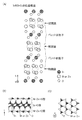
- FIG. 22 illustrates a crystal structure of InMZnO 4 (the element M is, for example, Al, Ga, Y, or Sn) included in the target 5230.
- FIG. 22A illustrates a crystal structure of InMZnO 4 when observed from a direction parallel to the b-axis.
- a repulsive force is generated between two adjacent M—Zn—O layers because the oxygen atom has a negative charge. Therefore, the InMZnO 4 crystal has a cleavage plane between two adjacent M—Zn—O layers.
- the ions 5201 generated in the high-density plasma region are accelerated toward the target 5230 by the electric field and eventually collide with the target 5230.
- the pellet 5200 which is flat or pellet-like sputtered particles, peels from the cleavage plane (see FIG. 21).
- the pellet 5200 is a portion sandwiched between two cleavage planes shown in FIG. Therefore, when only the pellet 5200 is extracted, the cross section becomes as shown in FIG. 22B and the top surface becomes as shown in FIG. Note that the structure of the pellet 5200 may be distorted by the impact of the collision of the ions 5201.
- the pellet 5200 is a flat or pellet-like sputtered particle having a triangular plane, for example, a regular triangular plane.
- the pellet 5200 is a flat or pellet-like sputtered particle having a hexagonal plane, for example, a regular hexagonal plane.
- the shape of the pellet 5200 is not limited to a triangle or a hexagon.
- the thickness of the pellet 5200 is determined according to the type of film forming gas.
- the pellet 5200 has a thickness of 0.4 nm to 1 nm, preferably 0.6 nm to 0.8 nm.
- the pellet 5200 has a width of 1 nm to 100 nm, preferably 2 nm to 50 nm, more preferably 3 nm to 30 nm.
- the ion 5201 is caused to collide with the target 5230 including an In-M-Zn oxide. Then, the pellet 5200 having three layers of an M—Zn—O layer, an In—O layer, and an M—Zn—O layer is peeled off.
- the particles 5203 are also ejected from the target 5230 as the pellet 5200 is peeled off.
- a particle 5203 has an aggregate of one atom or several atoms. Therefore, the particles 5203 can also be referred to as atomic particles.
- the surface When the pellet 5200 passes through the plasma 5240, the surface may be negatively or positively charged.
- the pellet 5200 may receive a negative charge from O 2 ⁇ in the plasma 5240.
- oxygen atoms on the surface of the pellet 5200 may be negatively charged.
- the pellet 5200 may grow by being combined with indium, the element M, zinc, oxygen, or the like in the plasma 5240 when passing through the plasma 5240.
- the pellets 5200 and particles 5203 that have passed through the plasma 5240 reach the surface of the substrate 5220. Note that part of the particles 5203 has a small mass and may be discharged to the outside by a vacuum pump or the like.
- the first pellet 5200 is deposited on the substrate 5220. Since the pellet 5200 is plate-shaped, the pellet 5200 is deposited with the plane side facing the surface of the substrate 5220. At this time, the charge on the surface of the pellet 5200 on the substrate 5220 side is released through the substrate 5220.
- the second pellet 5200 reaches the substrate 5220.
- the second pellet 5200 since the surface of the pellet 5200 already deposited and the surface of the second pellet 5200 are charged, forces that repel each other are generated.
- the second pellet 5200 is deposited with the plane side facing slightly away from the surface of the substrate 5220, avoiding the pellet 5200 that has already been deposited.
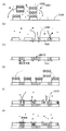
- innumerable pellets 5200 are deposited on the surface of the substrate 5220 by a thickness corresponding to one layer. Further, a region where the pellet 5200 is not deposited is generated between the pellets 5200 (see FIG. 23A).
- the particles 5203 that have received energy from the plasma reach the surface of the substrate 5220.
- the particles 5203 cannot be deposited on an active region such as the surface of the pellet 5200. Therefore, the particle 5203 moves to a region where the pellet 5200 is not deposited and adheres to the side surface of the pellet 5200.
- the bond 520 is activated by energy received from plasma, so that the particle 5203 is chemically connected to the pellet 5200 to form a lateral growth portion 5202 (see FIG. 23B).
- the pellets 5200 are connected by the lateral growth portion 5202 growing in the lateral direction (also referred to as lateral growth) (see FIG. 23C). In this manner, the lateral growth portion 5202 is formed until a region where the pellet 5200 is not deposited is filled.
- This mechanism is similar to the deposition mechanism of the atomic layer deposition (ALD) method.
- a new pellet 5200 is deposited with the plane side facing the surface (see FIG. 23D).
- the horizontal growth portion 5202 is formed by depositing the particles 5203 so as to fill a region where the pellet 5200 is not deposited (see FIG. 23E).
- the particles 5203 are attached to the side surfaces of the pellet 5200 and the lateral growth portion 5202 is laterally grown, thereby connecting the pellets 5200 in the second layer (see FIG. 23F).
- Film formation continues until the m-th layer (m is an integer of 2 or more) is formed, resulting in a thin film structure having a laminate.
- the method of depositing the pellet 5200 also varies depending on the surface temperature of the substrate 5220 and the like. For example, when the surface temperature of the substrate 5220 is high, the pellet 5200 undergoes migration on the surface of the substrate 5220. As a result, the proportion of the pellets 5200 that are connected without the particle 5203 interposed therebetween increases, so that a CAAC-OS with higher orientation is obtained.
- the surface temperature of the substrate 5220 when the CAAC-OS is formed is from room temperature to less than 340 ° C., preferably from room temperature to 300 ° C., more preferably from 100 ° C. to 250 ° C., and still more preferably from 100 ° C. to 200 ° C. is there. Therefore, even when a large-area substrate of the eighth generation or higher is used as the substrate 5220, warping due to the formation of the CAAC-OS film hardly occurs.
- the pellet 5200 when the surface temperature of the substrate 5220 is low, the pellet 5200 is less likely to cause migration on the surface of the substrate 5220. As a result, the pellets 5200 are stacked to form an nc-OS with low orientation. In the nc-OS, since the pellet 5200 is negatively charged, the pellet 5200 may be deposited at a constant interval. Therefore, although the orientation is low, a slight regularity results in a dense structure as compared with an amorphous oxide semiconductor.
- one large pellet may be formed due to the extremely small gap between the pellets.
- the inside of one large pellet has a single crystal structure.
- the size of the pellet may be 10 nm to 200 nm, 15 nm to 100 nm, or 20 nm to 50 nm when viewed from above.
- the pellets are deposited on the surface of the substrate by the film formation model as described above. Since the CAAC-OS film can be formed even when the formation surface does not have a crystal structure, it can be seen that the above-described film formation model, which is a growth mechanism different from epitaxial growth, has high validity. Further, since the above-described film formation model is used, it can be seen that the CAAC-OS and the nc-OS can form a uniform film even on a large-area glass substrate or the like. For example, the CAAC-OS can be formed even when the surface (formation surface) of the substrate has an amorphous structure (eg, amorphous silicon oxide).
- amorphous structure eg, amorphous silicon oxide
- the pellets are arranged along the shape.
- the following may be performed in order to form a highly crystalline CAAC-OS.
- the film is formed in a higher vacuum state.
- the plasma energy is weakened.
- thermal energy is applied to the surface to be formed, and the plasma damage is cured each time the film is formed.
- the above-described deposition model has a polycrystalline structure of a complex oxide such as an In-M-Zn oxide in which the target has a plurality of crystal grains, and any one of the crystal grains includes a cleavage plane. It is not limited to the case.
- the present invention can be applied to a case where a target of a mixture including indium oxide, an oxide of element M, and zinc oxide is used.
- the target of the mixture does not have a cleavage plane, the atomic particles peel off from the target when sputtered.
- a strong electric field region of plasma is formed in the vicinity of the target. Therefore, the atomic particles separated from the target are connected and grown laterally by the action of the strong electric field region of the plasma.
- indium which is an atomic particle, is connected and laterally grown to form a nanocrystal composed of an In—O layer.
- M-Zn-O layers are bonded to each other so as to complement the above.
- pellets may be formed even when a mixture target is used. Therefore, even when a mixture target is used, the above-described film formation model can be applied.
- the particles 5203 adhere (also referred to as bonding or adsorption) in the lateral direction of the pellet 5200 and laterally grow.
- FIG. 24A, 24B, 24C, 24D, and 24E are diagrams showing the structure of the pellet 5200 and the positions where metal ions adhere. It is assumed that the pellet 5200 is a cluster model in which 84 atoms are extracted from the crystal structure of InMZnO 4 while maintaining the stoichiometric composition. Hereinafter, the case where the element M is Ga will be described.
- FIG. 24F illustrates a structure of the pellet 5200 viewed from a direction parallel to the c-axis.
- FIG. 24G illustrates a structure of the pellet 5200 viewed from a direction parallel to the a-axis.
- the positions where metal ions adhere are indicated by position A, position B, position a, position b, and position c.
- position A is above the interstitial site surrounded by one gallium and two zincs on the upper surface of the pellet 5200.
- the position B is above the interstitial site surrounded by two galliums and one zinc on the upper surface of the pellet 5200.
- the position a is an indium site on the side surface of the pellet 5200.
- the position b is an interstitial site between the In—O layer and the Ga—Zn—O layer on the side surface of the pellet 5200.
- position c is a gallium site on the side surface of the pellet 5200.
- VASP Vehicle Ab initio Simulation Package
- PBE Perdew-Burke-Ernzerhof type generalized gradient approximation
- PAW Projector Augmented Wave
- Table 2 shows relative energies when indium ions (In 3+ ), gallium ions (Ga 3+ ), and zinc ions (Zn 2+ ) are arranged at position A, position B, position a, position b, and position c.
- the relative energy is a relative value when the energy of the model with the lowest energy is 0 eV in the calculated model.
- FIGS. 25A, 25B, 25C, 25D, and 25E are diagrams showing the structure of the pellet 5200 and the position where oxygen ions adhere.
- FIG. 25F illustrates a structure in which the pellet 5200 is viewed from a direction parallel to the c-axis.
- FIG. 25G illustrates a structure of the pellet 5200 viewed from a direction parallel to the b-axis.
- the position where oxygen ions adhere is indicated by position C, position D, position d, position e, and position f.
- the position C is a position where the upper surface of the pellet 5200 is bonded to gallium.
- the position D is a position where it is combined with zinc on the upper surface of the pellet 5200.
- the position d is a position where it is combined with indium on the side surface of the pellet 5200.
- the position e is a position where it is combined with gallium on the side surface of the pellet 5200.
- the position f is a position where it is combined with zinc on the side surface of the pellet 5200.
- Table 3 shows relative energies when oxygen ions (O 2 ⁇ ) are arranged at position C, position D, position d, position e, and position f.
- the particles 5203 approaching the pellet 5200 preferentially adhere to the side surface of the pellet 5200. That is, it can be said that the above-described film formation model in which the lateral growth of the pellet 5200 is caused by the particles 5203 attached to the side surface of the pellet 5200 has high validity.
- FIG. 26A is a top view of the transistor 200 which is a semiconductor device of one embodiment of the present invention
- FIG. 26B is a cross-sectional view taken along the dashed-dotted line X1-X2 in FIG. 26C corresponds to a cross-sectional view of a cross section taken along dashed-dotted line Y1-Y2 in FIG.
- some components such as an insulating film functioning as a gate insulating film
- the direction of the alternate long and short dash line X1-X2 may be referred to as a channel length direction, and the direction of the alternate long and short dash line Y1-Y2 may be referred to as a channel width direction. Note that in the top view of the transistor, some components may be omitted in the following drawings as in FIG. 26A.
- the transistor 200 includes a conductive film 204 functioning as a gate electrode over a substrate 202, an insulating film 206 over the substrate 202 and the conductive film 204, an insulating film 207 over the insulating film 206, and an oxide semiconductor film over the insulating film 207. 208, a conductive film 212a functioning as a source electrode electrically connected to the oxide semiconductor film 208, and a conductive film 212b functioning as a drain electrode electrically connected to the oxide semiconductor film 208.
- insulating films 214 and 216 and an insulating film 218 are provided over the transistor 200, more specifically, over the conductive films 212 a and 212 b and the oxide semiconductor film 208.
- the insulating films 214 and 216 and the insulating film 218 have a function as a protective insulating film of the transistor 200.
- the insulating film 206 and the insulating film 207 function as a gate insulating film of the transistor 200.
- the oxide semiconductor film 208 the oxide semiconductor film described in Embodiment 1 can be used. Since the oxide semiconductor film of one embodiment of the present invention is a highly crystalline oxide semiconductor film, the transistor 200 can be highly reliable.
- the substrate 202 There is no particular limitation on the material or the like of the substrate 202, but it is necessary to have at least heat resistance enough to withstand heat treatment performed later.
- a glass substrate, a ceramic substrate, a quartz substrate, a sapphire substrate, or the like may be used as the substrate 202.
- a single crystal semiconductor substrate made of silicon or silicon carbide, a polycrystalline semiconductor substrate, a compound semiconductor substrate such as silicon germanium, an SOI substrate, or the like can be applied, and a semiconductor element is provided over these substrates.
- the substrate 202 may be used.
- the sixth generation (1500 mm ⁇ 1850 mm), the seventh generation (1870 mm ⁇ 2200 mm), the eighth generation (2200 mm ⁇ 2400 mm), the ninth generation (2400 mm ⁇ 2800 mm), the tenth generation.
- a large-area substrate such as a generation (2950 mm ⁇ 3400 mm)
- a large display device can be manufactured. It is preferable to use such a large-area substrate because manufacturing costs can be reduced.
- a flexible substrate may be used as the substrate 202, and the transistor 200 may be formed directly over the flexible substrate.
- a separation layer may be provided between the substrate 202 and the transistor 200. The separation layer can be used for separation from the substrate 202 and transfer to another substrate after the semiconductor device is partially or entirely completed thereon. At that time, the transistor 200 can be transferred to a substrate having poor heat resistance or a flexible substrate.
- the conductive films 204, 212a, and 212b may have a single layer structure or a stacked structure of two or more layers.
- the conductive films 204, 212a, and 212b include indium tin oxide, indium oxide containing tungsten oxide, indium zinc oxide containing tungsten oxide, indium oxide containing titanium oxide, and indium tin oxide containing titanium oxide.
- a light-transmitting conductive material such as indium zinc oxide or indium tin oxide to which silicon oxide is added can be used.
- a Cu—X alloy film (X is Mn, Ni, Cr, Fe, Co, Mo, Ta, or Ti) may be applied to the conductive films 204, 212a, and 212b.
- X is Mn, Ni, Cr, Fe, Co, Mo, Ta, or Ti
- a Cu-X alloy film it can be processed by a wet etching process, and thus manufacturing costs can be suppressed.
- insulating film functioning as a gate insulating film As the insulating films 206 and 207 functioning as the gate insulating film of the transistor 200, a plasma enhanced chemical vapor deposition (PECVD) method, a sputtering method, or the like is used.
- PECVD plasma enhanced chemical vapor deposition
- Each insulating layer can be used. Note that instead of the stacked structure of the insulating films 206 and 207, a single-layer insulating film selected from the above materials or an insulating film having three or more layers may be used.
- the insulating film 206 has a function as a blocking film that suppresses permeation of oxygen.
- the insulating film 206 can suppress permeation of oxygen.
- the insulating film 207 in contact with the oxide semiconductor film 208 functioning as the channel region of the transistor 200 is preferably an oxide insulating film, and includes a region containing oxygen in excess of the stoichiometric composition (oxygen-excess region). ) Is more preferable.
- the insulating film 207 is an insulating film capable of releasing oxygen.
- the insulating film 207 may be formed in an oxygen atmosphere.
- oxygen may be introduced into the insulating film 207 after film formation to form an oxygen excess region.
- an ion implantation method, an ion doping method, a plasma immersion ion implantation method, a plasma treatment, or the like can be used.
- hafnium oxide has a higher dielectric constant than silicon oxide or silicon oxynitride. Accordingly, since the thickness of the insulating film 207 can be increased as compared with the case where silicon oxide is used, the leakage current due to the tunnel current can be reduced. That is, a transistor with a small off-state current can be realized. Further, hafnium oxide having a crystal structure has a higher dielectric constant than hafnium oxide having an amorphous structure. Therefore, in order to obtain a transistor with low off-state current, it is preferable to use hafnium oxide having a crystal structure. Examples of the crystal structure include a monoclinic system and a cubic system. Note that one embodiment of the present invention is not limited thereto.
- a silicon nitride film is formed as the insulating film 206 and a silicon oxide film is formed as the insulating film 207. Since the silicon nitride film has a relative dielectric constant higher than that of the silicon oxide film and has a large film thickness necessary for obtaining a capacitance equivalent to that of the silicon oxide film, the silicon nitride film is used as a gate insulating film of the transistor 200. Insulating film can be physically thickened. Accordingly, a decrease in the withstand voltage of the transistor 200 can be suppressed, and further, the withstand voltage can be improved, so that electrostatic breakdown of the transistor 200 can be suppressed.
- oxide semiconductor film As the oxide semiconductor film 208, the oxide semiconductor film of one embodiment of the present invention described in Embodiment 1 can be used.
- the energy gap of the oxide semiconductor film 208 is 2 eV or more, preferably 2.5 eV or more, more preferably 3 eV or more. In this manner, off-state current of the transistor 200 can be reduced by using an oxide semiconductor with a wide energy gap.
- the oxide semiconductor film 208 an oxide semiconductor film with low carrier density is used.
- the oxide semiconductor film 208 has a carrier density of less than 8 ⁇ 10 11 / cm 3 , preferably less than 1 ⁇ 10 11 / cm 3 , more preferably less than 1 ⁇ 10 10 / cm 3 , and 1 ⁇ 10 ⁇ It may be 9 / cm 3 or more.
- a transistor having an appropriate composition may be used depending on required semiconductor characteristics and electrical characteristics (such as field-effect mobility and threshold voltage) of a transistor.
- the carrier density, impurity concentration, defect density, atomic ratio of metal element to oxygen, interatomic distance, density, and the like of the oxide semiconductor film 208 are appropriate. It is preferable.
- an oxide semiconductor film with a low impurity concentration and a low density of defect states is preferably used because a transistor having more excellent electrical characteristics can be manufactured.
- low impurity concentration and low defect level density are referred to as high purity intrinsic or substantially high purity intrinsic.
- a highly purified intrinsic or substantially highly purified intrinsic oxide semiconductor film has few carrier generation sources, and thus can have a low carrier density. Therefore, a transistor in which a channel region is formed in the oxide semiconductor film rarely has electrical characteristics (also referred to as normally-on) in which the threshold voltage is negative.
- a highly purified intrinsic or substantially highly purified intrinsic oxide semiconductor film has a low density of defect states, and thus may have a low density of trap states.
- a highly purified intrinsic or substantially highly purified intrinsic oxide semiconductor film has an extremely small off-state current, a channel width of 1 ⁇ 10 6 ⁇ m, and a channel length L of 10 ⁇ m.
- the voltage between the drain electrodes is in the range of 1V to 10V, it is possible to obtain a characteristic that the off-current is less than the measurement limit of the semiconductor parameter analyzer, that is, 1 ⁇ 10 ⁇ 13 A or less.
- a transistor in which a channel region is formed in the high-purity intrinsic or substantially high-purity intrinsic oxide semiconductor film can be a highly reliable transistor with little variation in electrical characteristics.
- the charge trapped in the trap level of the oxide semiconductor film takes a long time to disappear, and may behave as if it were a fixed charge. Therefore, a transistor in which a channel region is formed in an oxide semiconductor film with a high trap state density may have unstable electrical characteristics.
- Impurities include hydrogen, nitrogen, alkali metal, alkaline earth metal, iron, nickel, silicon, and the like.
- Hydrogen contained in the oxide semiconductor film reacts with oxygen bonded to metal atoms to become water, and forms oxygen vacancies in a lattice from which oxygen is released (or a portion from which oxygen is released). When hydrogen enters the oxygen vacancies, electrons serving as carriers may be generated. In addition, a part of hydrogen may be combined with oxygen bonded to a metal atom to generate electrons as carriers. Therefore, a transistor including an oxide semiconductor film containing hydrogen is likely to be normally on. Therefore, it is preferable that hydrogen be reduced in the oxide semiconductor film 208 as much as possible.
- the hydrogen concentration obtained by secondary ion mass spectrometry (SIMS) in the oxide semiconductor film 208 is less than 1 ⁇ 10 20 atoms / cm 3 , preferably 1 ⁇ 10 19 atoms. / Cm 3 , more preferably 5 ⁇ 10 18 atoms / cm 3 , and even more preferably 1 ⁇ 10 18 atoms / cm 3 .
- the oxide semiconductor film 208 has a region where the hydrogen concentration obtained by SIMS is less than 1 ⁇ 10 20 atoms / cm 3 .
- the concentration of silicon or carbon in the oxide semiconductor film 208 and the concentration of silicon or carbon in the vicinity of the interface with the oxide semiconductor film 208 are 2 ⁇ 10 18 atoms / cm 3 or less, Preferably, it is 2 ⁇ 10 17 atoms / cm 3 or less.
- the alkali metal or the alkaline earth metal may be combined with the oxide semiconductor film to generate carriers. Therefore, a transistor including an oxide semiconductor film containing an alkali metal or an alkaline earth metal is likely to be normally on. Therefore, it is preferable to reduce the concentration of alkali metal or alkaline earth metal in the oxide semiconductor film 208.
- the concentration of alkali metal or alkaline earth metal in the oxide semiconductor film 208 obtained by SIMS is set to 1 ⁇ 10 18 atoms / cm 3 or less, preferably 2 ⁇ 10 16 atoms / cm 3 or less. .
- the oxide semiconductor film 208 contains iron, nickel, and silicon
- the iron nickel and silicon may be combined with the oxide semiconductor film to generate carriers. Therefore, a transistor including an oxide semiconductor film containing iron, nickel, and silicon is likely to be normally on. Therefore, it is preferable to reduce the concentration of iron, nickel, and silicon in the oxide semiconductor film 208.
- the total impurity concentration of iron, nickel, and silicon in the oxide semiconductor film 208 may be less than 0.03 atomic%.
- the oxide semiconductor film 208 when nitrogen is contained, electrons serving as carriers are generated, the carrier density is increased, and the oxide semiconductor film 208 is easily n-type. As a result, a transistor including an oxide semiconductor film containing nitrogen is likely to be normally on. Therefore, nitrogen in the oxide semiconductor film is preferably reduced as much as possible.
- the nitrogen concentration obtained by SIMS is preferably 5 ⁇ 10 18 atoms / cm 3 or less.
- the insulating films 214 and 216 have a function of supplying oxygen to the oxide semiconductor film 208.
- the insulating film 218 functions as a protective insulating film of the transistor 200.
- the insulating films 214 and 216 include oxygen.
- the insulating film 214 is an insulating film that can transmit oxygen. Note that the insulating film 214 also functions as a damage reducing film for the oxide semiconductor film 208 when the insulating film 216 to be formed later is formed.
- silicon oxide, silicon oxynitride, or the like with a thickness of 5 nm to 150 nm, preferably 5 nm to 50 nm can be used.
- the insulating film 214 preferably has a small amount of defects.
- the insulating film 214 can be formed using an oxide insulating film having a low level density due to nitrogen oxides.
- the level density due to the nitrogen oxide can be formed between the energy (Ev_os) at the upper end of the valence band of the oxide semiconductor film and the energy (Ec_os) at the lower end of the conduction band of the oxide semiconductor film.
- the oxide insulating film a silicon oxynitride film with a low emission amount of nitrogen oxide, an aluminum oxynitride film with a low emission amount of nitrogen oxide, or the like can be used.
- a silicon oxynitride film that emits less nitrogen oxide is a film that releases more ammonia than nitrogen oxide in a temperature programmed desorption gas analysis method, and typically releases ammonia molecules.
- the amount is 1 ⁇ 10 18 molecules / cm 3 or more and 5 ⁇ 10 19 molecules / cm 3 or less.
- the amount of ammonia released is the amount released by heat treatment at a film surface temperature of 50 ° C. to 650 ° C., preferably 50 ° C. to 550 ° C.
- Nitrogen oxide typically NO 2 or NO forms a level in the insulating film 214 or the like.
- the level is located in the energy gap of the oxide semiconductor film 208. Therefore, when nitrogen oxide diffuses to the interface between the insulating film 214 and the oxide semiconductor film 208, the level may trap electrons on the insulating film 214 side. As a result, trapped electrons remain in the vicinity of the interface between the insulating film 214 and the oxide semiconductor film 208, so that the threshold voltage of the transistor is shifted in the positive direction.
- nitrogen oxides react with ammonia and oxygen during heat treatment. Since nitrogen oxide contained in the insulating film 214 reacts with ammonia contained in the insulating film 216 in the heat treatment, nitrogen oxide contained in the insulating film 214 is reduced. Therefore, electrons are hardly trapped at the interface between the insulating film 214 and the oxide semiconductor film 208.
- a shift in threshold voltage of the transistor can be reduced, and variation in electrical characteristics of the transistor can be reduced.
- the insulating film 214 is measured with an ESR of 100 K or less by heat treatment in a transistor manufacturing process, typically less than 400 ° C. or less than 375 ° C. (preferably, 340 ° C. to 360 ° C.).
- a first signal having a g value of 2.037 to 2.039, a second signal having a g value of 2.001 to 2.003, and a g value of 1.964 to 1.966 The following third signal is observed.
- the split width of the first signal and the second signal and the split width of the second signal and the third signal are about 5 mT in the X-band ESR measurement.
- a first signal having a g value of 2.037 or more and 2.039 or less a second signal having a g value of 2.001 or more and 2.003 or less, and a first signal having a g value of 1.964 or more and 1.966 or less.
- the total density of the spins of the three signals is less than 1 ⁇ 10 18 spins / cm 3 , typically 1 ⁇ 10 17 spins / cm 3 or more and less than 1 ⁇ 10 18 spins / cm 3 .
- a third signal of .966 or less corresponds to a signal caused by nitrogen oxides (NO x , x is 0 or more and 2 or less, preferably 1 or more and 2 or less).
- nitrogen oxides include nitrogen monoxide and nitrogen dioxide. That is, a first signal having a g value of 2.037 to 2.039, a second signal having a g value of 2.001 to 2.003, and a first signal having a g value of 1.964 to 1.966. It can be said that the smaller the total density of the signal spins of 3, the smaller the content of nitrogen oxide contained in the oxide insulating film.
- the oxide insulating film has a nitrogen concentration measured by SIMS of 6 ⁇ 10 20 atoms / cm 3 or less.
- oxide insulating film By forming the oxide insulating film using a PECVD method using silane and dinitrogen monoxide with a substrate temperature of 220 ° C. or higher and 350 ° C. or lower, a dense and high hardness film is formed. be able to.
- the insulating film 216 is formed using an oxide insulating film containing more oxygen than that in the stoichiometric composition. Part of oxygen is released by heating from the oxide insulating film containing oxygen in excess of that in the stoichiometric composition.
- An oxide insulating film containing oxygen in excess of oxygen that satisfies the stoichiometric composition has an oxygen release amount converted to oxygen atoms by thermal desorption gas spectroscopy (TDS).
- the oxide insulating film has a thickness of 1.0 ⁇ 10 19 atoms / cm 3 or more, preferably 3.0 ⁇ 10 20 atoms / cm 3 or more.
- the surface temperature of the film in the TDS is preferably in the range of 100 ° C. to 700 ° C., or 100 ° C. to 500 ° C.
- silicon oxide, silicon oxynitride, or the like with a thickness of 30 nm to 500 nm, preferably 50 nm to 400 nm can be used.
- the insulating film 216 preferably has a small amount of defects.
- the insulating films 214 and 216 can be made of the same kind of insulating film, the interface between the insulating film 214 and the insulating film 216 may not be clearly confirmed. Therefore, in this embodiment, the interface between the insulating film 214 and the insulating film 216 is illustrated by a broken line. Note that although a two-layer structure of the insulating film 214 and the insulating film 216 has been described in this embodiment mode, the present invention is not limited thereto, and for example, a single-layer structure of the insulating film 214 or the insulating film 216 may be employed.
- the insulating film 218 has a function of blocking oxygen, hydrogen, water, alkali metal, alkaline earth metal, and the like.
- a nitride insulating film can be used as the insulating film 218, for example.
- the nitride insulating film include silicon nitride, silicon nitride oxide, aluminum nitride, and aluminum nitride oxide.
- an oxide insulating film having a blocking effect of oxygen, hydrogen, water, or the like may be provided instead of the nitride insulating film having a blocking effect of oxygen, hydrogen, water, alkali metal, alkaline earth metal, or the like.
- oxide insulating film having a blocking effect of oxygen, hydrogen, water, and the like examples include aluminum oxide, aluminum oxynitride, gallium oxide, gallium oxynitride, yttrium oxide, yttrium oxynitride, hafnium oxide, and hafnium oxynitride.
- FIG. 27A is a top view of a transistor 250 which is a semiconductor device of one embodiment of the present invention
- FIG. 27B is a cross-sectional view of a cross section taken along dashed-dotted line X1-X2 in FIG. 27C corresponds to a cross-sectional view of a cross section taken along dashed-dotted line Y1-Y2 in FIG. 27A.
- the transistor 250 includes a conductive film 204 functioning as a gate electrode over the substrate 202, an insulating film 206 over the substrate 202 and the conductive film 204, an insulating film 207 over the insulating film 206, and an oxide semiconductor film over the insulating film 207.
- a conductive film 204 functioning as a gate electrode over the substrate 202
- an insulating film 206 over the substrate 202 and the conductive film 204
- an insulating film 207 over the insulating film 206
- an oxide semiconductor film over the insulating film 207.
- An insulating film 218 is provided over the transistor 250, more specifically, over the conductive films 212 a and 212 b and the insulating film 216.
- the insulating films 214 and 216 function as protective insulating films for the oxide semiconductor film 208.
- the insulating film 218 functions as a protective insulating film of the transistor 250.
- the transistor 200 described above has a channel etch type structure, whereas the transistor 250 illustrated in FIGS. 27A, 27B, and 27C has a channel protection type structure.
- the oxide semiconductor film of one embodiment of the present invention can be applied to both a channel etch type transistor and a channel protection type transistor.
- Other configurations are the same as those of the transistor 200, and the same effects are obtained.
- FIG. 28A is a top view of the transistor 260 which is a semiconductor device of one embodiment of the present invention
- FIG. 28B is a cross-sectional view taken along the dashed-dotted line X1-X2 in FIG.
- FIG. 28C corresponds to a cross-sectional view taken along a dashed-dotted line Y1-Y2 in FIG.
- the transistor 260 includes a conductive film 204 functioning as a gate electrode over the substrate 202, an insulating film 206 over the substrate 202 and the conductive film 204, an insulating film 207 over the insulating film 206, and an oxide semiconductor film over the insulating film 207. 208, the insulating films 214 and 216 over the oxide semiconductor film 208, the conductive film 212a functioning as a source electrode electrically connected to the oxide semiconductor film 208, and the oxide semiconductor film 208. And a conductive film 212b functioning as a drain electrode.
- An insulating film 218 is provided over the transistor 260, more specifically, over the conductive films 212 a and 212 b and the insulating film 216.
- the insulating films 214 and 216 function as protective insulating films for the oxide semiconductor film 208.
- the insulating film 218 functions as a protective insulating film of the transistor 260.
- the transistor 260 is different from the transistor 250 illustrated in FIGS. 27A, 27B, and 27C in the shape of the insulating films 214 and 216. Specifically, the insulating films 214 and 216 of the transistor 260 are provided in an island shape over the channel region of the oxide semiconductor film 208. Other configurations are the same as those of the transistor 250, and the same effects are obtained.
- FIG. 29A is a top view of a transistor 270 which is a semiconductor device of one embodiment of the present invention
- FIG. 29B is a cross-sectional view taken along the dashed-dotted line X1-X2 in FIG.
- FIG. 29C corresponds to a drawing, and corresponds to a cross-sectional view of a cross section taken along the dashed-dotted line Y1-Y2 in FIG.
- the transistor 270 includes a conductive film 204 functioning as a first gate electrode over the substrate 202, an insulating film 206 over the substrate 202 and the conductive film 204, an insulating film 207 over the insulating film 206, and an oxide over the insulating film 207.
- a conductive film 212b functioning as a drain electrode connected to the conductive film 212; an insulating film 218 over the conductive films 212a and 212b and the insulating film 216; and conductive films 220a and 220b over the insulating film 218.
- the insulating films 214 and 216 and the insulating film 218 function as a second gate insulating film of the transistor 270.
- the conductive film 220a functions as a pixel electrode used for a display device, for example.
- the conductive film 220a is connected to the conductive film 212b through an opening 252c provided in the insulating films 214 and 216 and the insulating film 218.
- the conductive film 220b functions as a second gate electrode (also referred to as a back gate electrode).
- the conductive film 220b functions as a first gate electrode in the openings 252a and 252b provided in the insulating films 206 and 207, the insulating films 214 and 216, and the insulating film 218. Connected to the conductive film 204. Thus, the same potential is applied to the conductive film 220b and the conductive film 204.
- the present invention is not limited to this.
- a structure in which only one of the opening 252a and the opening 252b is formed and the conductive film 220b and the conductive film 204 are connected, or the conductive film 220b without the opening 252a and the opening 252b is provided.
- the conductive film 204 may not be connected. Note that in the case where the conductive film 220b and the conductive film 204 are not connected to each other, different potentials can be applied to the conductive film 220b and the conductive film 204, respectively.
- the oxide semiconductor film 208 is opposed to the conductive film 204 functioning as the first gate electrode and the conductive film 220b functioning as the second gate electrode. And sandwiched between conductive films functioning as two gate electrodes.
- the length in the channel length direction and the length in the channel width direction of the conductive film 220b functioning as the second gate electrode are longer than the length in the channel length direction and the length in the channel width direction of the oxide semiconductor film 208, respectively.
- the entire oxide semiconductor film 208 is covered with the conductive film 220 b with the insulating films 214 and 216 and the insulating film 218 interposed therebetween.
- the conductive film 220b functioning as the second gate electrode and the conductive film 204 functioning as the first gate electrode include an opening 252a provided in the insulating films 206 and 207, the insulating films 214 and 216, and the insulating film 218. , 252b, the side surface in the channel width direction of the oxide semiconductor film 208 is opposed to the conductive film 220b functioning as the second gate electrode with the insulating films 214 and 216 and the insulating film 218 interposed therebetween. .
- the conductive film 204 functioning as the first gate electrode and the conductive film 220b functioning as the second gate electrode include the insulating films 206 and 207 functioning as the gate insulating films and The insulating films 214 and 216 functioning as the second gate insulating film, and the insulating films 206 and 207 functioning as the gate insulating film and the insulating films functioning as the second gate insulating film while being connected in the openings provided in the insulating film 218
- the oxide semiconductor film 208 is surrounded by the films 214 and 216 and the insulating film 218.
- the oxide semiconductor film 208 included in the transistor 270 is electrically formed by the electric fields of the conductive film 204 functioning as the first gate electrode and the conductive film 220b functioning as the second gate electrode. Can be enclosed.
- a device structure of a transistor that electrically surrounds an oxide semiconductor film in which a channel region is formed by an electric field of the first gate electrode and the second gate electrode is referred to as a surround channel (s-channel) structure. Can be called.
- the transistor 270 Since the transistor 270 has an s-channel structure, an electric field for inducing a channel can be effectively applied to the oxide semiconductor film 208 by the conductive film 204 functioning as the first gate electrode. Current driving capability is improved, and high on-current characteristics can be obtained. Further, since the on-state current can be increased, the transistor 270 can be miniaturized. In addition, since the transistor 270 has a structure surrounded by the conductive film 204 functioning as the first gate electrode and the conductive film 220b functioning as the second gate electrode, the mechanical strength of the transistor 270 can be increased.
- FIGS. 30A and 30B are cross-sectional views of modifications of the transistor 270 illustrated in FIGS. 29B and 29C.
- FIGS. 30C and 30D are cross-sectional views of modifications of the transistor 270 illustrated in FIGS. 29B and 29C.
- the oxide semiconductor film 208 included in the transistor 270A includes an oxide semiconductor film 208a, an oxide semiconductor film 208b, and an oxide semiconductor film 208c.
- the oxide semiconductor film 208 included in the transistor 270B includes an oxide semiconductor film 208b and an oxide semiconductor film 208c.
- FIG. 31A illustrates an example of a band structure in the film thickness direction of a stacked structure including the insulating film 207, the oxide semiconductor films 208a, 208b, and 208c, and the insulating film 214.
- FIG. 31B illustrates an example of a band structure in the film thickness direction of a stacked structure including the insulating film 207, the oxide semiconductor films 208b and 208c, and the insulating film 214.
- the band structure indicates the energy level (Ec) of the lower end of the conduction band of the insulating film 207, the oxide semiconductor films 208a, 208b, and 208c, and the insulating film 214 for easy understanding.
- An oxide semiconductor film formed using an object target is used, and the oxide semiconductor film 208b is formed using a metal oxide
- the energy level at the lower end of the conduction band changes gently. In other words, it can be said that it is continuously changed or continuously joined.
- trap centers and recombination centers can be formed at the interface between the oxide semiconductor film 208a and the oxide semiconductor film 208b or at the interface between the oxide semiconductor film 208b and the oxide semiconductor film 208c. It is assumed that there is no impurity that forms such a defect level.
- a multi-chamber film formation apparatus sputtering apparatus including a load lock chamber is used so that each film is continuously exposed to the atmosphere. It is necessary to laminate them.
- the oxide semiconductor film 208b serves as a well, and a channel region is formed in the oxide semiconductor film 208b in the transistor including the above stacked structure. Recognize.
- trap levels that can be formed in the oxide semiconductor film 208b can be separated from the oxide semiconductor film 208b.
- the trap level may be farther from the vacuum level than the energy level (Ec) at the lower end of the conduction band of the oxide semiconductor film 208b functioning as the channel region, and electrons are likely to accumulate in the trap level. . Accumulation of electrons at the trap level results in a negative fixed charge, and the threshold voltage of the transistor shifts in the positive direction. Therefore, a structure in which the trap level is closer to the vacuum level than the energy level (Ec) at the lower end of the conduction band of the oxide semiconductor film 208b is preferable. By doing so, electrons are unlikely to accumulate in the trap level, the on-state current of the transistor can be increased, and field effect mobility can be increased.
- the oxide semiconductor films 208a and 208c have a lower energy level at the bottom of the conduction band than the oxide semiconductor film 208b, and typically the energy level at the bottom of the conduction band of the oxide semiconductor film 208b.
- the energy level at the lower end of the conduction band of the oxide semiconductor films 208a and 208c is 0.15 eV or more, 0.5 eV or more, 2 eV or less, or 1 eV or less. That is, the difference between the electron affinity of the oxide semiconductor films 208a and 208c and the electron affinity of the oxide semiconductor film 208b is 0.15 eV or more, 0.5 eV or more, and 2 eV or less, or 1 eV or less.
- the oxide semiconductor film 208b becomes a main current path. That is, the oxide semiconductor film 208b functions as a channel region, and the oxide semiconductor films 208a and 208c function as an oxide insulating film.
- the oxide semiconductor films 208a and 208c are oxide semiconductor films formed of one or more metal elements included in the oxide semiconductor film 208b in which a channel region is formed; Interface scattering hardly occurs at the interface with the semiconductor film 208b or at the interface between the oxide semiconductor film 208b and the oxide semiconductor film 208c. Accordingly, the movement of carriers is not inhibited at the interface, so that the field effect mobility of the transistor is increased.
- the oxide semiconductor films 208a and 208c are formed using a material with sufficiently low conductivity in order to prevent the oxide semiconductor films 208a and 208c from functioning as part of the channel region. Therefore, the oxide semiconductor films 208a and 208c can also be referred to as oxide insulating films because of their physical properties and / or functions.
- the oxide semiconductor films 208a and 208c have an electron affinity (difference between the vacuum level and the energy level at the bottom of the conduction band) smaller than that of the oxide semiconductor film 208b, and the energy level at the bottom of the conduction band is an oxide.
- a material having a difference (band offset) from the lower energy level of the conduction band of the semiconductor film 208b is used.
- the energy level at the lower end of the conduction band of the oxide semiconductor films 208a and 208c is reduced by the conduction of the oxide semiconductor film 208b. It is preferable to use a material closer to the vacuum level than the energy level at the lower end of the band.
- the difference between the energy level at the bottom of the conduction band of the oxide semiconductor film 208b and the energy level at the bottom of the conduction band of the oxide semiconductor films 208a and 208c is 0.2 eV or more, preferably 0.5 eV or more. It is preferable.
- the oxide semiconductor films 208a and 208c do not include a spinel crystal structure.
- the constituent elements of the conductive films 212a and 212b enter the oxide semiconductor film 208b at the interface between the spinel crystal structure and another region. May diffuse.
- the oxide semiconductor films 208a and 208c be a CAAC-OS because a blocking property of a constituent element of the conductive films 212a and 212b, for example, a copper element is increased.
- the thickness of the oxide semiconductor films 208a and 208c is greater than or equal to a thickness that can prevent the constituent elements of the conductive films 212a and 212b from diffusing into the oxide semiconductor film 208b.
- the thickness is less than the thickness at which the supply of oxygen to the film 208b is suppressed.
- the thickness of the oxide semiconductor films 208a and 208c is 10 nm or more, the constituent elements of the conductive films 212a and 212b can be prevented from diffusing into the oxide semiconductor film 208b.
- the thickness of the oxide semiconductor films 208a and 208c is 100 nm or less, oxygen can be effectively supplied from the insulating film 214 to the oxide semiconductor film 208b.
- the structure using a physical semiconductor film has been illustrated, it is not limited to this.
- the oxide semiconductor film 208 included in the transistors 200 and 270 and the oxide semiconductor film 208c included in the transistors 270A and 270B are thinned in regions exposed from the conductive films 212a and 212b in the drawing.
- a shape in which part of the oxide semiconductor film has a recess is illustrated.
- the oxide semiconductor film in the region exposed from the conductive films 212a and 212b may not have a depression.
- 32A, 32B, 32C, and 32D are cross-sectional views illustrating an example of a semiconductor device.
- FIGS. 32A and 32B illustrate a structure in which the oxide semiconductor film 208 of the transistor 200 described above does not have a depression
- FIGS. 32C and 32D illustrate the oxidation of the transistor 270B described above.
- the physical semiconductor film 208 does not have a recess.
- each of the above structures can be freely combined.
- various films such as a conductive film, an insulating film, and an oxide semiconductor film included in the semiconductor device of one embodiment of the present invention can be formed by a sputtering method, a chemical vapor deposition (CVD) method, or a plasma chemical vapor deposition (PECVD). , Vacuum evaporation, and pulsed laser deposition (PLD).
- the present invention is not limited to this, and may be formed by, for example, a coating method, a printing method, a thermal CVD (Chemical Vapor Deposition) method, or an atomic layer deposition (ALD: Atomic Layer Deposition) method.
- a conductive film, an insulating film, an oxide semiconductor film, or the like may be formed using a MOCVD (Metal Organic Chemical Vapor Deposition) method or the like.
- the thermal CVD method has an advantage that no defects are generated due to plasma damage because it is a film forming method that does not use plasma.
- film formation may be performed by sending a source gas and an oxidant into the chamber at the same time, making the inside of the chamber under atmospheric pressure or reduced pressure, reacting in the vicinity of the substrate or on the substrate and depositing on the substrate. .
- film formation may be performed by setting the inside of the chamber to atmospheric pressure or reduced pressure, sequentially introducing source gases for reaction into the chamber, and repeating the order of gas introduction.
- each switching valve also referred to as a high-speed valve
- An active gas such as argon or nitrogen
- a second source gas is introduced.
- the inert gas becomes a carrier gas, and the inert gas may be introduced at the same time when the second raw material gas is introduced.
- the second raw material gas may be introduced after the first raw material gas is exhausted by evacuation.
- the first source gas is adsorbed on the surface of the substrate to form a first layer, reacts with a second source gas introduced later, and the second layer is stacked on the first layer.
- a thin film is formed.
- the thermal CVD method such as the MOCVD method can form various films such as the conductive film, the insulating film, the oxide semiconductor film, and the metal oxide film of the above embodiment.
- an In—Ga—ZnO film is formed.
- trimethylindium, trimethylgallium, and dimethylzinc are used.
- the chemical formula of trimethylindium is In (CH 3 ) 3 .
- the chemical formula of trimethylgallium is Ga (CH 3 ) 3 .
- the chemical formula of dimethylzinc is Zn (CH 3 ) 2 .
- Triethylgallium (chemical formula Ga (C 2 H 5 ) 3 ) can be used instead of trimethylgallium, and diethylzinc (chemical formula Zn (C 2 H 5 ) is used instead of dimethylzinc. 2 ) can also be used.
- hafnium oxide film when a hafnium oxide film is formed by a film forming apparatus using ALD, a raw material obtained by vaporizing a liquid (hafnium amide such as hafnium alkoxide or tetrakisdimethylamide hafnium (TDMAH)) containing a solvent and a hafnium precursor compound.
- hafnium amide such as hafnium alkoxide or tetrakisdimethylamide hafnium (TDMAH)
- TDMAH tetrakisdimethylamide hafnium
- Two types of gas, ozone and ozone (O 3 ) are used as an oxidizing agent.
- the chemical formula of tetrakisdimethylamide hafnium is Hf [N (CH 3 ) 2 ] 4 .
- Other material liquids include tetrakis (ethylmethylamide) hafnium.
- a source gas obtained by vaporizing a liquid such as trimethylaluminum (TMA)
- TMA trimethylaluminum
- H 2 a solvent and an aluminum precursor compound
- gases of O Two kinds of gases of O are used.
- trimethylaluminum is Al (CH 3 ) 3 .
- Other material liquids include tris (dimethylamido) aluminum, triisobutylaluminum, aluminum tris (2,2,6,6-tetramethyl-3,5-heptanedionate) and the like.
- hexachlorodisilane is adsorbed on the film formation surface, chlorine contained in the adsorbate is removed, and an oxidizing gas (O 2 , monoxide) Dinitrogen) radicals are supplied to react with the adsorbate.
- oxidizing gas O 2 , monoxide
- tungsten film is formed by a film forming apparatus using ALD
- an initial tungsten film is formed by repeatedly introducing WF 6 gas and B 2 H 6 gas successively, and then WF 6 gas and H 2.
- a tungsten film is formed using a gas.
- SiH 4 gas may be used instead of B 2 H 6 gas.
- an oxide semiconductor film such as an In—Ga—ZnO film is formed by a film formation apparatus using ALD
- In (CH 3 ) 3 gas and O 3 gas are sequentially introduced and In—O is sequentially introduced.
- a GaO layer is formed using Ga (CH 3 ) 3 gas and O 3 gas
- a ZnO layer is formed using Zn (CH 3 ) 2 gas and O 3 gas.
- a mixed compound layer such as an In—Ga—O layer, an In—Zn—O layer, or a Ga—Zn—O layer may be formed by mixing these gases.
- O 3 may be used of H 2 O gas obtained by bubbling with an inert gas such as Ar in place of the gas, but better to use an O 3 gas containing no H are preferred.
- In (C 2 H 5 ) 3 gas may be used instead of In (CH 3 ) 3 gas.
- Ga (C 2 H 5 ) 3 gas may be used instead of Ga (CH 3 ) 3 gas.
- Zn (CH 3 ) 2 gas may be used.
- FIGS. 33A to 33F FIGS. 34A to 34F, and FIGS. 35A to 35F are cross-sectional views illustrating a method for manufacturing a semiconductor device. It is. 33 (A), (C), and (E), FIGS. 34 (A), (C), and (E) and FIGS. 35 (A), (C), and (E) are cross-sectional views in the channel length direction. 33 (B) (D) (F), FIGS. 34 (B) (D) (F), and FIGS. 35 (B) (D) (F) are cross-sectional views in the channel width direction.
- a conductive film is formed over the substrate 202, and the conductive film is processed by a lithography process and an etching process, so that a conductive film 204 functioning as a gate electrode is formed.
- insulating films 206 and 207 functioning as gate insulating films are formed over the conductive film 204 (see FIGS. 33A and 33B).
- a glass substrate is used as the substrate 202, and a tungsten film with a thickness of 100 nm is formed as the conductive film 204 functioning as a gate electrode by a sputtering method.
- a 400-nm-thick silicon nitride film is formed as the insulating film 206 by PECVD, and a 50-nm-thick silicon oxynitride film is formed as the insulating film 207 by PECVD.
- the insulating film 206 can have a stacked structure of silicon nitride films. Specifically, the insulating film 206 can have a three-layer structure including a first silicon nitride film, a second silicon nitride film, and a third silicon nitride film. As an example of the three-layer structure, it can be formed as follows.
- the first silicon nitride film for example, silane having a flow rate of 200 sccm, nitrogen having a flow rate of 2000 sccm, and ammonia gas having a flow rate of 100 sccm are supplied as source gases to the reaction chamber of the PE-CVD apparatus, and the pressure in the reaction chamber is controlled to 100 Pa. Then, a power of 2000 W may be supplied using a 27.12 MHz high frequency power source so that the thickness is 50 nm.
- silane having a flow rate of 200 sccm, nitrogen having a flow rate of 2000 sccm, and ammonia gas having a flow rate of 2000 sccm are supplied as source gases to the reaction chamber of the PECVD apparatus, and the pressure in the reaction chamber is controlled to 100 Pa;
- a thickness of 300 nm may be formed by supplying 2000 W of power using a 12 MHz high frequency power source.
- silane having a flow rate of 200 sccm and nitrogen having a flow rate of 5000 sccm are supplied as source gases to the reaction chamber of the PECVD apparatus, the pressure in the reaction chamber is controlled to 100 Pa, and a high frequency power source of 27.12 MHz is used. Then, the power may be formed so as to have a thickness of 50 nm by supplying power of 2000 W.
- the substrate temperature when forming the first silicon nitride film, the second silicon nitride film, and the third silicon nitride film can be 350 ° C. or lower.
- the insulating film 206 has a three-layer structure of a silicon nitride film, for example, when a conductive film containing copper (Cu) is used for the conductive film 204, the following effects can be obtained.
- the first silicon nitride film can suppress diffusion of the copper (Cu) element from the conductive film 204.
- the second silicon nitride film has a function of releasing hydrogen and can improve the withstand voltage of the insulating film functioning as a gate insulating film.
- the third silicon nitride film emits less hydrogen from the third silicon nitride film and can suppress diffusion of hydrogen released from the second silicon nitride film.
- the insulating film 207 is preferably formed using an insulating film containing oxygen in order to improve interface characteristics with the oxide semiconductor film 208 (more specifically, the oxide semiconductor film 208b) to be formed later.
- an oxide semiconductor film stacked film is formed over the insulating film 207, and the stacked film is processed into a desired shape, whereby the island-shaped oxide semiconductor film 208b and the oxide semiconductor film 208c are formed.
- An oxide semiconductor film 208 is formed (see FIGS. 33C and 33D).
- the temperature at which the oxide semiconductor film 208 is formed is from room temperature to less than 340 ° C., preferably from room temperature to 300 ° C., more preferably from 100 ° C. to 250 ° C., and even more preferably from 100 ° C. to 200 ° C. .
- the temperature at which the oxide semiconductor film 208 is formed is 150 ° C. or higher and lower than 340 ° C. 202 may be deformed (distorted or warped). Therefore, in the case where a large glass substrate is used, deformation of the glass substrate can be suppressed by setting the temperature at which the oxide semiconductor film 208 is formed to be greater than or equal to 100 ° C. and less than 150 ° C.
- the substrate temperatures at the time of forming the oxide semiconductor film 208b and the oxide semiconductor film 208c may be the same or different. Note that it is preferable that the substrate temperatures of the oxide semiconductor film 208b and the oxide semiconductor film 208c be the same because manufacturing costs can be reduced.
- An oxide semiconductor film to be the oxide semiconductor film 208c is formed by a method.
- the substrate temperature at the time of forming the oxide semiconductor film to be the oxide semiconductor film 208 is set to 170 ° C.
- oxygen and argon are used as a deposition gas for forming the oxide semiconductor film to be the oxide semiconductor film 208.
- a rare gas typically argon
- oxygen, a rare gas, and a mixed gas of oxygen are appropriately used as a sputtering gas.
- a mixed gas it is preferable to increase the oxygen gas ratio relative to the rare gas.
- oxygen gas or argon gas used as a sputtering gas is a gas having a dew point of ⁇ 40 ° C. or lower, preferably ⁇ 80 ° C. or lower, more preferably ⁇ 100 ° C. or lower, more preferably ⁇ 120 ° C. or lower.
- the sputtering gas preferably contains oxygen.
- oxygen can be added to the lower layer film (here, the insulating film 207) at the same time as the formation of the oxide semiconductor film. It becomes. Therefore, an oxygen excess region can be provided in the insulating film 207.
- the chamber in the sputtering apparatus is provided with an adsorption-type vacuum exhaust pump such as a cryopump so as to remove water or the like which is an impurity for the oxide semiconductor film as much as possible. It is preferable to use and evacuate a high vacuum (from about 5 ⁇ 10 ⁇ 7 Pa to about 1 ⁇ 10 ⁇ 4 Pa). Alternatively, it is preferable to combine a turbo molecular pump and a cold trap so that a gas, particularly a gas containing carbon or hydrogen, does not flow backward from the exhaust system into the chamber.
- a conductive film 212 to be a source electrode and a drain electrode is formed over the insulating film 207 and the oxide semiconductor film 208 by a sputtering method (see FIGS. 33E and 33F).
- a stacked film in which a 50-nm-thick tungsten film and a 400-nm-thick aluminum film are sequentially stacked is formed as the conductive film 212 by a sputtering method.
- the conductive film 212 may have a three-layer structure in which a 50-nm-thick tungsten film, a 400-nm-thick aluminum film, and a 100-nm-thick titanium film are sequentially stacked.
- the conductive film 212 is processed into a desired shape, thereby forming conductive films 212a and 212b separated from each other (see FIGS. 34A and 34B).
- the conductive film 212 is processed using a dry etching apparatus.
- the method for processing the conductive film 212 is not limited to this, and for example, a wet etching apparatus may be used.
- a finer pattern can be formed by processing the conductive film 212 by using a dry etching apparatus than by processing the conductive film 212 by using a wet etching apparatus.
- the manufacturing cost can be reduced by processing the conductive film 212 using a wet etching apparatus rather than processing the conductive film 212 using a dry etching apparatus.
- the surface (back channel side) of the oxide semiconductor film 208 may be cleaned.
- the cleaning method include cleaning using a chemical solution such as phosphoric acid.
- a chemical solution such as phosphoric acid
- impurities attached to the surface of the oxide semiconductor film 208c eg, elements contained in the conductive films 212a and 212b
- the cleaning is not necessarily performed, and in some cases, the cleaning may not be performed.
- a region exposed from the conductive films 212a and 212b of the oxide semiconductor film 208 may be thin.
- a region where the thickness of the oxide semiconductor film 208c is smaller than that of the oxide semiconductor film 208b may be formed.
- the insulating film 214 and the insulating film 216 are formed over the oxide semiconductor film 208 and the conductive films 212a and 212b (see FIGS. 34C and 34D).
- the insulating film 216 is preferably formed continuously without being exposed to the air.
- the insulating film 214 and the insulating film are formed by continuously forming the insulating film 216 by adjusting one or more of the flow rate, pressure, high frequency power, and substrate temperature of the source gas without opening to the atmosphere.
- the concentration of impurities derived from atmospheric components can be reduced at the interface with H.216, and oxygen contained in the insulating films 214 and 216 can be moved to the oxide semiconductor film 208. The amount can be reduced.
- a silicon oxynitride film can be formed by a PECVD method.
- a deposition gas and an oxidation gas containing silicon as the source gas.
- the deposition gas containing silicon include silane, disilane, trisilane, and fluorinated silane.
- the oxidizing gas include dinitrogen monoxide and nitrogen dioxide.
- the PECVD method in which the flow rate of the oxidizing gas with respect to the flow rate of the deposition gas is set to be greater than 20 times and less than 100 times, preferably 40 times or more and 80 times or less, and the pressure in the processing chamber is less than 100 Pa, preferably 50 Pa or less.
- the insulating film 214 contains nitrogen and has a small amount of defects.
- the temperature for holding the substrate 202 is 220 ° C.
- silane having a flow rate of 50 sccm and dinitrogen monoxide having a flow rate of 2000 sccm are used as source gas
- the pressure in the processing chamber is 20 Pa
- parallel plates A silicon oxynitride film is formed by a PECVD method in which high-frequency power supplied to the electrode is 13.56 MHz and 100 W (power density is 1.6 ⁇ 10 ⁇ 2 W / cm 2 ).
- the substrate placed in the evacuated processing chamber of the PECVD apparatus is held at 180 ° C. or higher and 350 ° C. or lower, and a raw material gas is introduced into the processing chamber so that the pressure in the processing chamber is 100 Pa or higher and 250 Pa or lower. , more preferably not more than 200Pa than 100 Pa, the electrode provided in the processing chamber 0.17 W / cm 2 or more 0.5 W / cm 2 or less, more preferably 0.25 W / cm 2 or more 0.35 W / cm 2 or less of A silicon oxide film or a silicon oxynitride film is formed depending on conditions for supplying high-frequency power.
- the decomposition efficiency of the source gas in plasma is increased, oxygen radicals are increased, and the oxidation of the source gas proceeds. Therefore, the oxygen content in the insulating film 216 is higher than the stoichiometric composition.
- the bonding force between silicon and oxygen is weak, part of oxygen in the film is released by heat treatment in a later step. As a result, an oxide insulating film containing more oxygen than that in the stoichiometric composition and from which part of oxygen is released by heating can be formed.
- the insulating film 214 serves as a protective film for the oxide semiconductor film 208 in the step of forming the insulating film 216. Therefore, the insulating film 216 can be formed using high-frequency power with high power density while reducing damage to the oxide semiconductor film 208.
- the amount of defects in the insulating film 216 can be reduced by increasing the flow rate of the deposition gas containing silicon with respect to the oxidizing gas under the deposition conditions of the insulating film 216.
- An oxide insulating layer with a small amount of defects that is preferably 1.5 ⁇ 10 17 spins / cm 3 or less can be formed. As a result, the reliability of the transistor can be improved.
- first heat treatment heat treatment
- nitrogen oxides contained in the insulating films 214 and 216 can be reduced.
- part of oxygen contained in the insulating films 214 and 216 can be moved to the oxide semiconductor film 208 by the first heat treatment, so that the amount of oxygen vacancies contained in the oxide semiconductor film 208 can be reduced.
- the temperature of the first heat treatment is typically less than 400 ° C, preferably less than 375 ° C, and more preferably 150 ° C to 350 ° C.
- the first heat treatment is performed in an atmosphere of nitrogen, oxygen, ultra-dry air (air with a water content of 20 ppm or less, preferably 1 ppm or less, preferably 10 ppb or less), or a rare gas (such as argon or helium). Just do it.
- an electric furnace, RTA (Rapid Thermal Anneal), or the like can be used for the heat treatment in which nitrogen, oxygen, ultra-dry air, or a rare gas preferably contains no hydrogen, water, or the like.
- the barrier film 230 is formed over the insulating film 216, and oxygen 240 is added to the insulating films 216 and 214 or the oxide semiconductor film 208 through the barrier film 230 (see FIGS. 34E and 34F). ).
- oxygen added to the insulating film 214 or the insulating film 216 is schematically indicated by broken-line arrows.
- the barrier film 230 has a function of transmitting oxygen and suppressing release of oxygen.
- the barrier film 230 includes, for example, oxygen and a metal (at least one selected from indium, zinc, titanium, aluminum, tungsten, tantalum, molybdenum, hafnium, and yttrium).
- a metal at least one selected from indium, zinc, titanium, aluminum, tungsten, tantalum, molybdenum, hafnium, and yttrium.
- ITO indium tin oxide
- ITSO indium tin silicon oxide
- indium oxide coverage with unevenness is favorable. This is preferable.
- the barrier film 230 can be formed using a sputtering method.
- the thickness of the barrier film 230 is preferably 1 nm to 20 nm, or 2 nm to 10 nm.
- ITSO with a thickness of 5 nm is formed as the barrier film 230.
- oxygen 240 As a method for adding oxygen 240 to the insulating film 216 through the barrier film 230, there are an ion doping method, an ion implantation method, a plasma treatment method, and the like. Further, depending on a device for adding oxygen 240 or conditions for adding oxygen, oxygen 240 may be added to the insulating film 214 or the oxide semiconductor film 208 located below the insulating film 216 in some cases. Examples of the oxygen 240 include excess oxygen or oxygen radicals. In addition, when the oxygen 240 is added, the oxygen 240 can be effectively added to the insulating film 216 by applying a bias to the substrate side.
- an ashing device may be used as the bias, and the power density of the bias applied to the ashing device may be 1 W / cm 2 or more and 5 W / cm 2 or less.
- the barrier film 230 functions as a protective film that suppresses release of oxygen from the insulating film 216. Therefore, more oxygen can be added to the insulating film 216.
- heat treatment (hereinafter referred to as second heat treatment) may be performed after adding oxygen 240 to the insulating film 216 through the barrier film 230.
- the second heat treatment can be the same as the first heat treatment described above.
- an insulating film 218 is formed over the insulating film 216 (see FIGS. 35A and 35B).
- the barrier film 230 when the barrier film 230 is removed, part of the insulating film 216 may also be removed.
- the method for removing the barrier film 230 include a dry etching method, a wet etching method, or a method in which the dry etching method and the wet etching method are combined.
- the barrier film 230 is removed using a wet etching method.
- the insulating film 218 can be formed using, for example, a sputtering method or a PECVD method.
- the substrate temperature is lower than 400 ° C., preferably lower than 375 ° C., more preferably 180 ° C. or higher and 350 ° C. or lower. It is preferable to set the substrate temperature in the case of forming the insulating film 218 within the above range because a dense film can be formed.
- oxygen or excess oxygen in the insulating films 214 and 216 can be transferred to the oxide semiconductor film 208.
- a heat treatment equivalent to the second heat treatment described above (hereinafter referred to as a third heat treatment) may be performed.
- heat treatment is performed at a temperature of less than 400 ° C., preferably less than 375 ° C., more preferably 180 ° C. or more and 350 ° C. or less. Oxygen or excess oxygen can be moved into the oxide semiconductor film 208 (in particular, the oxide semiconductor film 208b) so that oxygen vacancies in the oxide semiconductor film 208 can be filled.
- FIGS. 36 illustrates an oxide semiconductor film formed by the substrate temperature (typically less than 375 ° C.) at the time of forming the insulating film 218 or the third heat treatment (typically less than 375 ° C.) after the insulating film 218 is formed.
- 3 is a model diagram showing oxygen moving into a film 208.
- oxygen oxygen radicals, oxygen atoms, or oxygen molecules
- FIG. 36 oxygen (oxygen radicals, oxygen atoms, or oxygen molecules) in the oxide semiconductor film 208 is represented by dashed arrows.
- oxygen vacancies are compensated by movement of oxygen from films in contact with the oxide semiconductor film 208 (here, the insulating film 207 and the insulating film 214).
- the oxide semiconductor film 208 when the oxide semiconductor film 208 is formed by sputtering, oxygen gas is used and oxygen is added to the insulating film 206; thus, the insulating film 207 has an excess oxygen region.
- the insulating films 214 and 216 since oxygen is added through the barrier film 230, the insulating films 214 and 216 have excess oxygen regions. Therefore, the oxide semiconductor film 208 sandwiched between insulating films having excess oxygen regions can appropriately fill oxygen vacancies in the oxide semiconductor film 208.
- an insulating film 206 is provided below the insulating film 207, and an insulating film 218 is provided above the insulating films 214 and 216.
- oxygen contained in the insulating films 207, 214, and 216 can be confined to the oxide semiconductor film 208 side. Oxygen can be preferably transferred to the oxide semiconductor film 208.
- a silicon nitride film is formed as the insulating film 218 by PECVD
- a deposition gas containing silicon, nitrogen, and ammonia as a source gas.
- ammonia is dissociated in the plasma and active species are generated.
- the active species breaks the bond between silicon and hydrogen contained in the deposition gas containing silicon and the triple bond of nitrogen. As a result, the bonding between silicon and nitrogen is promoted, the bonding between silicon and hydrogen is small, the defects are few, and a dense silicon nitride film can be formed.
- the flow rate ratio of nitrogen to ammonia is preferably 5 to 50 times and 10 to 50 times.
- a 50-nm-thick silicon nitride film is formed as the insulating film 218 by using a PECVD apparatus and using silane, nitrogen, and ammonia as source gases.
- the flow rates are 50 sccm for silane, 5000 sccm for nitrogen, and 100 sccm for ammonia.
- the processing chamber pressure is 100 Pa
- the substrate temperature is 350 ° C.
- high frequency power of 1000 W is supplied to the parallel plate electrodes using a high frequency power source of 27.12 MHz.
- PECVD apparatus is a PECVD apparatus of a parallel plate type electrode area is 6000 cm 2, which is in terms 1.7 ⁇ 10 -1 W / cm 2 to the power per unit area power supplied (power density).
- a mask is formed over the insulating film 218 by a lithography process, and an opening 252c is formed in a desired region of the insulating films 214, 216, and 218. Further, a mask is formed over the insulating film 218 by a lithography process, and openings 252a and 252b are formed in desired regions of the insulating films 206, 207, 214, 216, and 218. Note that the opening 252c is formed so as to reach the conductive film 212b. The openings 252a and 252b are formed so as to reach the conductive film 204, respectively (see FIGS. 35C and 35D).
- the openings 252a and 252b and the opening 252c may be formed in the same process or in different processes. In the case where the openings 252a and 252b and the opening 252c are formed in the same step, for example, a gray-tone mask or a halftone mask can be used. Further, the openings 252a and 252b may be formed in a plurality of times. For example, an opening may be formed in the insulating films 206 and 207 in advance, and then the insulating films 214, 216, and 218 over the openings may be opened.
- a conductive film is formed over the insulating film 218 so as to cover the openings 252a, 252b, and 252c, and the conductive film is processed into a desired shape, whereby the conductive films 220a and 220b are formed (FIG. 35 ( (See E) and (F).)
- the conductive film to be the conductive films 220a and 220b for example, a material containing one kind selected from indium (In), zinc (Zn), and tin (Sn) can be used.
- the conductive films 220a and 220b include indium oxide containing tungsten oxide, indium zinc oxide containing tungsten oxide, indium oxide containing titanium oxide, indium tin oxide containing titanium oxide, indium tin oxide (ITO ), A light-transmitting conductive material such as indium zinc oxide and indium tin silicon oxide (ITSO) can be used.
- the conductive film to be the conductive films 220a and 220b can be formed by, for example, a sputtering method. In this embodiment, ITSO with a thickness of 110 nm is formed by a sputtering method.
- the transistor 270B illustrated in FIGS. 30C and 30D can be manufactured.
- the substrate temperature is lower than 400 ° C., preferably lower than 375 ° C., more preferably 180 ° C. or higher and 350 ° C. or lower. This is preferable because distortion or warpage can be extremely reduced.
- the substrate temperature at the time of forming the insulating films 206 and 207 (less than 400 ° C., preferably 250 ° C. to 350 ° C.)
- the substrate temperature at the time of forming the oxide semiconductor film 208 room temperature to less than 340 ° C., preferably 100 ° C. to 200 ° C., more preferably 100 ° C.
- Temperature (less than 400 ° C., preferably less than 375 ° C., more preferably 180 ° C. or more and 350 ° C. or less), first heat treatment or second heat treatment after addition of oxygen 240 (less than 400 ° C., preferably less than 375 ° C. And more preferably 180 ° C. or higher and 350 ° C. or lower).
- barrier film 230 a highly insulating material may be selected from the materials described above.
- barrier film 230 used in one embodiment of this manufacturing method aluminum oxide, hafnium oxide, or yttrium oxide is preferably used.
- the barrier film 230 is formed using aluminum oxide, hafnium oxide, or yttrium oxide by a sputtering method, it is preferable that at least oxygen be included as a sputtering gas.
- oxygen is used as a sputtering gas when the barrier film 230 is formed, the oxygen becomes oxygen radicals in the plasma, and either or both of the oxygen and the oxygen radicals are added to the insulating film 216. There is. Therefore, the step of adding oxygen 240 illustrated in FIGS. 34E and 34F is not necessarily performed. In other words, when the barrier film 230 is formed, the oxygen addition treatment and the formation of the barrier film 230 can be performed simultaneously.
- the barrier film 230 has a function of adding oxygen during the formation of the barrier film 230 (particularly at the initial stage of film formation), but blocks oxygen after the formation of the barrier film 230 (particularly at the later stage of film formation). It has the function to do.
- a mixed layer may be formed in the vicinity of the interface between the insulating film 216 and the barrier film 230.
- the insulating film 216 is a silicon oxynitride film
- Al x Si y O z can be formed as the mixed layer. Note that the mixed layer may have an excess oxygen region.
- the barrier film 230 when aluminum oxide, hafnium oxide, or yttrium oxide is used as the barrier film 230, aluminum oxide, hafnium oxide, and yttrium oxide have high insulating properties and high oxygen barrier properties. Therefore, the step of forming the insulating film 218 illustrated in FIGS. 35A and 35B may not be performed. Accordingly, the insulating film 218 may be used as it is without removing the barrier film 230.
- the substrate temperature at the time of forming the barrier film 230 to less than 400 ° C., preferably less than 375 ° C., more preferably 180 ° C. to 350 ° C., oxygen or excess oxygen added to the insulating film 216 can be reduced.
- the oxide semiconductor film 208 can be moved.
- the manufacturing process of the semiconductor device can be shortened, and the manufacturing cost can be suppressed.
- FIGS. 37A to 37F and FIGS. 38A to 38F are cross-sectional views illustrating a method for manufacturing a semiconductor device.
- 37A, 37C, 38E, and 38A, 38C, 38E are cross-sectional views in the channel length direction
- FIGS. 38B, 38D, and 38F are cross-sectional views in the channel width direction.
- a conductive film 204, insulating films 206 and 207, an oxide semiconductor film 208, insulating films 214 and 216, and a barrier film 230 are formed over the substrate 202 (see FIGS. 37A and 37B).
- the conductive film 204, the insulating films 206 and 207, the oxide semiconductor film 208, the insulating films 214 and 216, and the barrier film 230 may be formed in consideration of the description of [Method 1 for manufacturing a semiconductor device].
- oxygen 240 is added to the insulating film 214 through the barrier film 230 (see FIGS. 37C and 37D).
- the barrier film 230 is removed.
- a mask is formed over the insulating film 214 by a lithography process, and openings 251a and 251b are formed in desired regions of the insulating film 214. Note that the openings 251a and 251b reach the oxide semiconductor film 208 (see FIGS. 37E and 37F).
- a conductive film 212 is formed over the oxide semiconductor film 208 and the insulating film 214 so as to cover the openings 251a and 251b (see FIGS. 38A and 38B).
- a mask is formed over the conductive film 212 by a lithography process, and the conductive film is processed into a desired shape, thereby forming conductive films 212a and 212b (see FIGS. 38C and 38D).
- an insulating film 218 is formed over the insulating film 214 and the conductive films 212a and 212b (see FIGS. 38E and 38F).
- the transistor 250 illustrated in FIGS. 27A, 27B, and 27C can be manufactured.
- the insulating film 214 is formed only over the channel region of the oxide semiconductor film 208 in the step of forming the openings 251a and 251b. It can produce.
- FIGS. 4 a sputtering apparatus and a deposition apparatus that can form the oxide semiconductor film of one embodiment of the present invention will be described with reference to FIGS. Note that the sputtering apparatus described below is shown in a state where a substrate, a target, and the like are arranged in order to explain an operation during film formation. However, since the substrate, the target, and the like are appropriately installed by the practitioner, the sputtering apparatus may not have the substrate and the target.
- a parallel plate sputtering apparatus and a counter target sputtering apparatus can be used as the sputtering apparatus.
- a film formation method using a parallel plate sputtering apparatus can also be called PESP (parallel electrode SP).
- a film formation method using an opposed target sputtering apparatus can also be referred to as VDSP (vapor deposition SP).
- FIG. 39A is a cross-sectional view of the film formation chamber 301 in the parallel plate sputtering apparatus.
- a film formation chamber 301 illustrated in FIG. 39A includes a target holder 320, a backing plate 310, a target 300, a magnet unit 330, and a substrate holder 370.
- the target 300 is disposed on the backing plate 310.
- the backing plate 310 is disposed on the target holder 320.
- the magnet unit 330 is disposed under the target 300 via the backing plate 310.
- the substrate holder 370 is disposed to face the target 300.
- the magnet unit can be called a cathode, a cathode magnet, a magnetic member, a magnetic component, or the like.
- the magnet unit 330 includes a magnet 330N, a magnet 330S, and a magnet holder 332. In the magnet unit 330, the magnet 330N and the magnet 330S are disposed on the magnet holder 332. Further, the magnet 330N is arranged at a distance from the magnet 330S. Note that when the substrate 360 is carried into the film formation chamber 301, the substrate 360 is disposed in contact with the substrate holder 370.
- the target holder 320 and the backing plate 310 are fixed using screws (bolts or the like) and are equipotential.
- the target holder 320 has a function of supporting the target 300 via the backing plate 310.
- the target 300 is fixed to the backing plate 310.
- the backing plate 310 and the target 300 can be fixed by a bonding material containing a low melting point metal such as indium.
- FIG. 39A shows magnetic lines of force 380 a and magnetic lines 380 b formed by the magnet unit 330.
- the magnetic field line 380a is one of the magnetic field lines that form a horizontal magnetic field in the vicinity of the upper surface of the target 300.
- the vicinity of the upper surface of the target 300 is, for example, a region having a vertical distance from the target 300 of 0 mm to 10 mm, particularly 0 mm to 5 mm.
- Magnetic field lines 380b are one of magnetic field lines that form a horizontal magnetic field at a vertical distance d from the upper surface of the magnet unit 330.
- the vertical distance d is, for example, 0 mm or more and 20 mm or less, or 5 mm or more and 15 mm or less.
- a strong magnetic field can be generated even in the vicinity of the substrate 360 by using the strong magnet 330N and the strong magnet 330S.
- the strength of the horizontal magnetic field in the vicinity of the substrate 360 can be set to 10G to 100G, preferably 15G to 60G, and more preferably 20G to 40G.
- the horizontal magnetic field strength may be measured by measuring the value when the vertical magnetic field strength is 0G.
- the obtained oxide semiconductor film hardly includes a plurality of types of crystal phases, and becomes an oxide semiconductor film including almost a single crystal phase.
- FIG. 39B shows a top view of the magnet unit 330.
- a circular or substantially circular magnet 330 ⁇ / b> N and a circular or substantially circular magnet 330 ⁇ / b> S are fixed to a magnet holder 332.
- the magnet unit 330 can be rotated using the center or substantially center normal vector on the upper surface of the magnet unit 330 as a rotation axis.
- the magnet unit 330 may be rotated at a beat of 0.1 Hz to 1 kHz (in other words, rhythm, time signature, pulse, frequency, period, or cycle).
- the strong magnetic field region on the target 300 changes as the magnet unit 330 rotates. Since the region where the magnetic field is strong becomes a high-density plasma region, the sputtering phenomenon of the target 300 tends to occur in the vicinity thereof. For example, when a region with a strong magnetic field is a specific location, only a specific region of the target 300 is used. On the other hand, the target 300 can be uniformly used by rotating the magnet unit 330 as shown in FIG. Further, by rotating the magnet unit 330, a film having a uniform thickness and a film having a uniform quality can be obtained.
- the direction of the lines of magnetic force in the vicinity of the substrate 360 can be changed.
- the magnet unit 330 may be swung up and down or / and left and right.
- the magnet unit 330 may be swung with a beat of 0.1 Hz to 1 kHz.
- the target 300 may be rotated or moved.
- the target 300 may be rotated or oscillated with a beat of 0.1 Hz to 1 kHz.
- the direction of the magnetic lines of force in the vicinity of the substrate 360 may be relatively changed by rotating the substrate 360. Or you may combine these.
- the film formation chamber 301 may have a groove in the inside or the bottom of the backing plate 310. Then, by flowing a fluid (air, nitrogen, rare gas, water, oil, etc.) through the groove, discharge abnormalities due to a rise in the temperature of the target 300 during sputtering and damage to the film formation chamber 301 due to deformation of members are suppressed. can do. At this time, it is preferable that the backing plate 310 and the target 300 are brought into close contact with each other via a bonding material because the cooling performance is improved.
- a fluid air, nitrogen, rare gas, water, oil, etc.
- a gasket be provided between the target holder 320 and the backing plate 310 because impurities are less likely to enter the film formation chamber 301 from the outside or a groove.
- the magnet 330N and the magnet 330S are arranged with different poles facing the target 300 side.
- the magnet 330N is arranged so that the target 300 side has an N pole
- the magnet 330S is arranged so that the target 300 side has an S pole.
- the arrangement of magnets and poles in the magnet unit 330 is not limited to this arrangement. Further, the arrangement is not limited to that shown in FIG.
- the potential applied to the terminal V1 connected to the target holder 320 is, for example, a lower potential than the potential applied to the terminal V2 connected to the substrate holder 370.
- the potential applied to the terminal V2 connected to the substrate holder 370 is, for example, a ground potential.
- the potential applied to the terminal V3 connected to the magnet holder 332 is, for example, a ground potential.
- the potential applied to the terminal V1, the terminal V2, and the terminal V3 is not limited to the above potential. Further, the potential may not be applied to all of the target holder 320, the substrate holder 370, and the magnet holder 332.
- the substrate holder 370 may be in a floating state. Note that although FIG.
- 39A illustrates an example of a so-called DC sputtering method in which a potential is applied to the terminal V1 connected to the target holder 320
- the present invention is not limited thereto.
- a so-called RF sputtering method in which a high-frequency power source having a frequency of 13.56 MHz or 27.12 MHz is connected to the target holder 320 may be used.
- FIG. 39A shows an example in which the backing plate 310 and the target holder 320 are not electrically connected to the magnet unit 330 and the magnet holder 332, but the present invention is not limited to this.
- the backing plate 310 and the target holder 320, and the magnet unit 330 and the magnet holder 332 may be electrically connected and may be equipotential.
- the temperature of the substrate 360 may be increased in order to further increase the crystallinity of the obtained oxide semiconductor film.
- the temperature of the substrate 360 is, for example, room temperature to less than 340 ° C., preferably room temperature to 300 ° C., more preferably 100 ° C. to 250 ° C., and further preferably 100 ° C. to 200 ° C.
- the vertical distance between the target 300 and the substrate 360 is 10 mm to 600 mm, preferably 20 mm to 400 mm, more preferably 30 mm to 200 mm, and more preferably 40 mm to 100 mm.
- a decrease in energy before the sputtered particles reach the substrate 360 may be suppressed.
- the incident direction of the sputtered particles on the substrate 360 can be made closer to the vertical, so that damage to the substrate 360 due to the collision of the sputtered particles can be reduced. Sometimes it can be made smaller.
- FIG. 40A shows an example of a deposition chamber different from that in FIG.
- a deposition chamber 301 illustrated in FIG. 40A includes a target holder 320a, a target holder 320b, a backing plate 310a, a backing plate 310b, a target 300a, a target 300b, a magnet unit 330a, and a magnet unit 330b. , A member 342, and a substrate holder 370.
- the target 300a is disposed on the backing plate 310a.
- the backing plate 310a is disposed on the target holder 320a.
- the magnet unit 330a is arrange
- the target 300b is disposed on the backing plate 310b.
- the backing plate 310b is disposed on the target holder 320b.
- the magnet unit 330b is arrange
- the magnet unit 330a includes a magnet 330N1, a magnet 330N2, a magnet 330S, and a magnet holder 332.
- the magnet 330N1, the magnet 330N2, and the magnet 330S are disposed on the magnet holder 332. Further, the magnet 330N1 and the magnet 330N2 are arranged with a gap from the magnet 330S.
- the magnet unit 330b has the same structure as the magnet unit 330a. Note that when the substrate 360 is carried into the film formation chamber 301, the substrate 360 is disposed in contact with the substrate holder 370.
- the target 300a, the backing plate 310a, and the target holder 320a are separated from the target 300b, the backing plate 310b, and the target holder 320b by a member 342.
- the member 342 is preferably an insulator.
- the member 342 may be a conductor or a semiconductor.
- the member 342 may be a conductor or a semiconductor whose surface is covered with an insulator.
- the target holder 320a and the backing plate 310a are fixed using screws (bolts or the like) and are equipotential. Further, the target holder 320a has a function of supporting the target 300a via the backing plate 310a. Further, the target holder 320b and the backing plate 310b are fixed using screws (bolts or the like) and are equipotential. Further, the target holder 320b has a function of supporting the target 300b via the backing plate 310b.
- the backing plate 310a has a function of fixing the target 300a.
- the backing plate 310b has a function of fixing the target 300b.
- FIG. 40A shows magnetic lines of force 380a and magnetic lines 380b formed by the magnet unit 330a.
- the magnetic field line 380a is one of the magnetic field lines that form a horizontal magnetic field in the vicinity of the target 300a.
- the vicinity of the target 300a is, for example, a region having a vertical distance from the target 300a of 0 mm to 10 mm, particularly 0 mm to 5 mm.
- Magnetic field lines 380b are one of the magnetic field lines that form a horizontal magnetic field at a vertical distance d from the upper surface of the magnet unit 330a.
- the vertical distance d is, for example, 0 mm or more and 20 mm or less, or 5 mm or more and 15 mm or less.
- a strong magnetic field can be generated even in the vicinity of the substrate 360 by using the strong magnet 330N1, the magnet 330N2, and the strong magnet 330S.
- the strength of the horizontal magnetic field in the vicinity of the substrate 360 can be set to 10G to 100G, preferably 15G to 60G, and more preferably 20G to 40G.
- an oxide semiconductor film with high density and high crystallinity can be formed.
- the obtained oxide semiconductor film rarely includes a plurality of types of crystal phases and becomes an oxide including almost a single crystal phase.
- the magnet unit 330b also has the same magnetic lines as the magnet unit 330a.
- FIG. 40B shows a top view of the magnet unit 330a and the magnet unit 330b.
- the magnet unit 330 a has a rectangular or substantially rectangular magnet 330 ⁇ / b> N ⁇ b> 1, a rectangular or substantially rectangular magnet 330 ⁇ / b> N ⁇ b> 2, and a rectangular or substantially rectangular magnet 330 ⁇ / b> S fixed to the magnet holder 332.
- the magnet unit 330a can be swung left and right as shown in FIG.
- the magnet unit 330a may be swung with a beat of 0.1 Hz to 1 kHz.
- the strong magnetic field region on the target 300a changes as the magnet unit 330a swings. Since the region where the magnetic field is strong becomes a high-density plasma region, the sputtering phenomenon of the target 300a tends to occur in the vicinity thereof. For example, when a region with a strong magnetic field is a specific location, only a specific region of the target 300a is used. On the other hand, as shown in FIG. 40B, the target 300a can be used uniformly by swinging the magnet unit 330a. Further, by swinging the magnet unit 330a, a film having a uniform thickness and a film having a uniform quality can be obtained.
- the state of the lines of magnetic force in the vicinity of the substrate 360 can be changed by swinging the magnet unit 330a.
- the magnet unit 330a and the magnet unit 330b may be rotated.
- the magnet unit 330a and the magnet unit 330b may be rotated at a beat of 0.1 Hz to 1 kHz.
- the target 300 may be rotated or moved.
- the target 300 may be rotated or oscillated with a beat of 0.1 Hz to 1 kHz.
- the state of the lines of magnetic force on the upper surface of the substrate 360 can be relatively changed by rotating the substrate 360. Alternatively, these may be combined.
- the film formation chamber 301 may have a groove portion inside or below the backing plate 310a and the backing plate 310b. Then, by flowing a fluid (air, nitrogen, rare gas, water, oil, etc.) through the groove, discharge abnormality due to a rise in the temperature of the target 300a and the target 300b during sputtering, or damage to the film formation chamber 301 due to deformation of members. Etc. can be suppressed.
- a fluid air, nitrogen, rare gas, water, oil, etc.
- Etc. can be suppressed.
- the backing plate 310a and the target 300a are in close contact with each other through a bonding material because the cooling performance is improved.
- the backing plate 310b and the target 300b are in close contact with each other through a bonding material because the cooling performance is improved.
- the magnet 330N1, the magnet 330N2, and the magnet 330S are arranged with different poles facing the target 300a.
- the magnet 330N1 and the magnet 330N2 are arranged so that the target 300a side has an N pole
- the magnet 330S is arranged so that the target 300a side has an S pole.
- the arrangement of the magnets and poles in the magnet unit 330a is not limited to this arrangement. Further, the arrangement is not limited to that shown in FIG. The same applies to the magnet unit 303b.
- a potential at which the level is alternately switched may be applied between the terminal V1 connected to the target holder 320a and the terminal V4 connected to the target holder 320b.
- the potential applied to the terminal V2 connected to the substrate holder 370 is, for example, a ground potential.
- the potential applied to the terminal V3 connected to the magnet holder 332 is, for example, a ground potential. Note that the potential applied to the terminal V1, the terminal V2, the terminal V3, and the terminal V4 is not limited to the above potential. Further, the potential may not be applied to all of the target holder 320a, the target holder 320b, the substrate holder 370, and the magnet holder 332. For example, the substrate holder 370 may be in a floating state.
- FIG. 40A an example of a so-called AC sputtering method in which a potential that alternates between high and low is applied between a terminal V1 connected to the target holder 320a and a terminal V4 connected to the target holder 320b. Although shown, it is not limited to this.
- the backing plate 310a and the target holder 320a are not electrically connected to the magnet unit 330a and the magnet holder 332, but the present invention is not limited to this.
- the backing plate 310a and the target holder 320a, and the magnet unit 330a and the magnet holder 332 may be electrically connected and may be equipotential.
- the backing plate 310b and the target holder 320b are not electrically connected to the magnet unit 330b and the magnet holder 332 has been shown, it is not limited thereto.
- the backing plate 310a and the target holder 320b, and the magnet unit 330b and the magnet holder 332 may be electrically connected and may be equipotential.
- the temperature of the substrate 360 may be increased in order to further increase the crystallinity of the obtained oxide semiconductor film.
- the temperature of the substrate 360 is, for example, room temperature to less than 340 ° C., preferably room temperature to 300 ° C., more preferably 100 ° C. to 250 ° C., and further preferably 100 ° C. to 200 ° C.
- the vertical distance between the target 300a and the substrate 360 is 10 mm to 600 mm, preferably 20 mm to 400 mm, more preferably 30 mm to 200 mm, and more preferably 40 mm to 100 mm.
- a decrease in energy before the sputtered particles reach the substrate 360 may be suppressed.
- the incident direction of the sputtered particles to the substrate 360 can be made closer to the vertical, so that damage to the substrate 360 due to the collision of the sputtered particles can be reduced. Sometimes it can be made smaller.
- the vertical distance between the target 300b and the substrate 360 is set to 10 mm to 600 mm, preferably 20 mm to 400 mm, more preferably 30 mm to 200 mm, more preferably 40 mm to 100 mm.
- a decrease in energy before the sputtered particles reach the substrate 360 may be suppressed.
- the incident direction of the sputtered particles on the substrate 360 can be made closer to the vertical, so that damage to the substrate 360 due to the collision of the sputtered particles can be reduced. Sometimes it can be made smaller.
- FIG. 41A is a cross-sectional view of the film formation chamber in the facing target sputtering apparatus.
- 41A includes a target 300a and a target 300b, a backing plate 310a and a backing plate 310b that respectively hold the target 300a and the target 300b, and the target 300a and the target through the backing plate 310a and the backing plate 310b.
- a magnet unit 330a and a magnet unit 330b disposed on the back surface of the target 300b;
- the substrate holder 370 is disposed between the target 300a and the target 300b. Note that when the substrate 360 is placed in the deposition chamber, the substrate 360 is fixed by the substrate holder 370.
- a power source 390 and a power source 391 for applying a potential are connected to the backing plate 310a and the backing plate 310b. It is preferable to use a so-called AC power source in which a potential at which the potential level is alternately switched is applied between a power source 390 connected to the backing plate 310a and a power source 391 connected to the backing plate 310b.
- the power supply 390 and the power supply 391 which are shown in FIG. 41 show the example using AC power supply, it is not restricted to this.
- an RF power source, a DC power source, or the like may be used as the power source 390 and the power source 391.
- different types of power sources may be used for the power source 390 and the power source 391.
- the substrate holder 370 is preferably connected to GND. Further, the substrate holder 370 may be in a floating state.
- FIG. 41B and 41C show the potential distribution of the plasma 340 between the alternate long and short dash line AB in FIG. 41A.
- the potential distribution shown in FIG. 41B shows a state in which a high potential is applied to the backing plate 310a and a low potential is applied to the backing plate 310b. That is, positive ions are accelerated toward the target 300b.
- the potential distribution shown in FIG. 41C shows a state in which a low potential is applied to the backing plate 310a and a high potential is applied to the backing plate 310b. That is, positive ions are accelerated toward the target 300a. Film formation can be performed so that the states of FIG. 41B and FIG. 41C are alternately switched.
- a state where the substrate holder 370 and the substrate 360 are arranged in the plasma 340 is preferable.
- the substrate holder 370 and the substrate 360 be disposed in the positive column region in the plasma 340.
- the region of the positive column in the plasma 340 is a region where the gradient of the potential distribution is small in the potential distributions shown in FIGS. 41B and 41C. That is, as shown in FIG. 41A, the substrate 360 is not exposed to the strong electric field portion under the plasma 340 by disposing the substrate 360 in the positive column region in the plasma 340, so that the substrate 360 is damaged by the plasma 340. Therefore, defects can be reduced.
- the horizontal distance between the substrate holder 370 and the target 300a is L1
- the horizontal distance between the substrate holder 370 and the target 300b is L2.
- the lengths of L1 and L2 are preferably the same length as the substrate 360, respectively.
- L1 and L2 may be 10 mm or more and 200 mm or less, respectively.
- the target 300a and the target 300b are arranged to face each other in parallel.
- the magnet unit 330a and the magnet unit 330b are arrange
- the lines of magnetic force are directed from the magnet unit 330b to the magnet unit 330a. Therefore, at the time of film formation, the plasma 340 is confined in the magnetic field formed by the magnet unit 330a and the magnet unit 330b.
- the substrate holder 370 and the substrate 360 are arranged in a region (also referred to as an inter-target region) between the target 300a and the target 300b facing each other.
- a region also referred to as an inter-target region
- the substrate holder 370 and the substrate 360 are arranged in parallel to the direction in which the target 300a and the target 300b face each other, but they may be arranged at an angle. For example, by tilting the substrate holder 370 and the substrate 360 by 30 ° or more and 60 ° or less (typically 45 °), the ratio of sputtered particles that are perpendicularly incident on the substrate 360 during film formation can be increased.
- the configuration shown in FIG. 42 is different from the configuration shown in FIG. 41A in that the target 300a and the target 300b are not parallel to each other but are arranged to face each other in an inclined state (in a V shape). Therefore, the description of FIG. 41A is referred to except for the target arrangement. Further, the magnet unit 330a and the magnet unit 330b are arranged so that different poles face each other. The substrate holder 370 and the substrate 360 are disposed in the inter-target region. By arranging the target 300a and the target 300b as shown in FIG. 42, the ratio of sputtered particles reaching the substrate 360 is increased, so that the deposition rate can be increased.
- the substrate holder 370 and the substrate 360 are disposed in the plasma 340, but the present invention is not limited to this.
- the substrate holder 370 and the substrate 360 may be disposed outside the plasma 340. Since the substrate 360 is not exposed to the high electric field region of the plasma 340, damage due to the plasma 340 can be reduced. However, the use efficiency of the target 300a and the target 300b decreases as the substrate 360 is separated from the plasma 340. Further, it is preferable that the position of the substrate holder 370 is variable as shown in FIG.
- the substrate holder 370 is disposed on the upper side of the inter-target region, it may be disposed on the lower side. Moreover, you may arrange
- the opposed target type sputtering apparatus can stably generate plasma even in a high vacuum. For example, film formation is possible even at 0.005 Pa or more and 0.09 Pa or less. Therefore, the concentration of impurities mixed during film formation can be reduced.
- a highly crystalline film can be formed even when the temperature of the substrate 360 is low.
- a highly crystalline film can be formed even when the temperature of the substrate 360 is higher than or equal to room temperature and lower than 100 ° C.
- FIG. 44 (A) shows another example of a counter target type sputtering apparatus.
- FIG. 44A is a schematic cross-sectional view of a film formation chamber in an opposed target sputtering apparatus. Unlike the deposition chamber illustrated in FIG. 41A, a target shield 322 and a target shield 323 are provided. In addition, a power source 391 connected to the backing plate 310a and the backing plate 310b is provided.
- the target shield 322a and the target shield 322b are connected to GND. That is, the plasma 340 is formed by the potential difference applied between the backing plate 310a and the backing plate 310b to which the potential of the power source 391 is applied and the target shield 322a and the target shield 322b to which GND is applied.
- a state where the substrate holder 370 and the substrate 360 are arranged in the plasma 340 is preferable.
- the substrate holder 370 and the substrate 360 be disposed in the positive column region in the plasma 340.
- the positive column region in the plasma is a region where the gradient of the potential distribution is small. That is, as shown in FIG. 44A, the substrate 360 is not exposed to the strong electric field portion under the plasma 340 by disposing the substrate 360 in the positive column region in the plasma 340. Therefore, the substrate 360 is not damaged by the plasma 340. Less oxide with good film quality can be obtained.
- the horizontal distance between the substrate holder 370 and the target 300a is L1
- the horizontal distance between the substrate holder 370 and the target 300b is L2.
- the lengths of L1 and L2 are each preferably equal to the size of the substrate 360.
- the present invention is not limited to this.
- the substrate holder 370 and the substrate 360 may be arranged outside the plasma 340. Since the substrate 360 is not exposed to the high electric field region of the plasma 340, damage due to the plasma 340 can be reduced. However, the use efficiency of the target 300a and the target 300b decreases as the substrate 360 is separated from the plasma 340.
- the position of the substrate holder 370 is preferably variable as shown in FIG.
- the substrate holder 370 is arranged on the upper side of the region where the target 300a and the target 300b face each other, but it may be arranged on the lower side. Moreover, you may arrange
- the counter target type sputtering apparatus described above can reduce plasma damage to the substrate because the plasma is confined to the magnetic field between the targets. Further, since the incident angle of the sputtered particles on the substrate can be made shallow by the inclination of the target, the step coverage of the deposited film can be improved. In addition, since film formation in a high vacuum is possible, the concentration of impurities mixed in the film can be reduced.
- a parallel plate sputtering apparatus or an ion beam sputtering apparatus may be applied to the film formation chamber.
- FIG. 45 the structure of a film formation apparatus in which impurities are hardly mixed in the film during film formation will be described with reference to FIGS. 45 and 46.
- FIG. 45 the structure of a film formation apparatus in which impurities are hardly mixed in the film during film formation will be described with reference to FIGS. 45 and 46.
- FIG. 45 schematically shows a top view of a single-wafer multi-chamber film forming apparatus 2700.
- the film formation apparatus 2700 includes an atmosphere-side substrate supply chamber 2701 that includes a cassette port 2761 that accommodates a substrate and an alignment port 2762 that aligns the substrate, and an atmosphere-side substrate that transports the substrate from the atmosphere-side substrate supply chamber 2701.
- an unload lock chamber 2703b for switching from atmospheric pressure to reduced pressure a transfer chamber 2704 for transferring a substrate in a vacuum, a substrate heating chamber 2705 for heating the substrate, and a film formation chamber 2706a for forming a film with a target disposed.
- a film formation chamber 2706b and a film formation chamber 2706c Note that the above-described structure of the film formation chamber can be referred to for the film formation chamber 2706a, the film formation chamber 2706b, and the film formation chamber 2706c.
- the atmosphere-side substrate transfer chamber 2702 is connected to the load lock chamber 2703a and the unload lock chamber 2703b, the load lock chamber 2703a and the unload lock chamber 2703b are connected to the transfer chamber 2704, and the transfer chamber 2704 is heated to the substrate.
- the chamber 2705, the film formation chamber 2706a, the film formation chamber 2706b, and the film formation chamber 2706c are connected.
- a gate valve 2764 is provided at a connection portion of each chamber, and each chamber can be kept in a vacuum state independently of the atmosphere side substrate supply chamber 2701 and the atmosphere side substrate transfer chamber 2702.
- the atmosphere-side substrate transfer chamber 2702 and the transfer chamber 2704 have a transfer robot 2763 and can transfer a substrate.
- the substrate heating chamber 2705 also serves as a plasma processing chamber.
- the film formation apparatus 2700 can transport the substrate between the processes without being exposed to the atmosphere, and thus can suppress the adsorption of impurities to the substrate.
- the order of film formation and heat treatment can be established freely. Note that the number of transfer chambers, film formation chambers, load lock chambers, unload lock chambers, and substrate heating chambers is not limited to the above-described numbers, and an optimal number can be provided as appropriate according to installation space and process conditions.
- FIG. 46 shows a cross section corresponding to one-dot chain line V1-V2, one-dot chain line W1-W2, and one-dot chain line W2-W3 shown in FIG.
- FIG. 46A shows a cross section of the substrate heating chamber 2705 and the transfer chamber 2704, and the substrate heating chamber 2705 includes a plurality of heating stages 2765 that can accommodate substrates.
- the substrate heating chamber 2705 is connected to a vacuum pump 2770 through a valve.
- a vacuum pump 2770 for example, a dry pump, a mechanical booster pump, or the like can be used.
- a heating mechanism that can be used for the substrate heating chamber 2705 for example, a heating mechanism that heats using a resistance heating element or the like may be used.
- a heating mechanism that heats by heat conduction or heat radiation from a medium such as a heated gas may be used.
- RTA such as GRTA (Gas Rapid Thermal Anneal) and LRTA (Lamp Rapid Thermal Anneal) can be used.
- LRTA heats an object to be processed by radiation of light (electromagnetic waves) emitted from a lamp such as a halogen lamp, a metal halide lamp, a xenon arc lamp, a carbon arc lamp, a high pressure sodium lamp, or a high pressure mercury lamp.
- GRTA performs heat treatment using a high-temperature gas. An inert gas is used as the gas.
- the substrate heating chamber 2705 is connected to the purifier 2781 via the mass flow controller 2780.
- the mass flow controller 2780 and the purifier 2781 are provided as many as the number of gas types, but only one is shown for easy understanding.
- a gas having a dew point of ⁇ 80 ° C. or lower, preferably ⁇ 100 ° C. or lower can be used.
- oxygen gas, nitrogen gas, and rare gas (such as argon gas) can be used. Use.
- the transfer chamber 2704 has a transfer robot 2863.
- the transfer robot 2763 can transfer a substrate to each chamber.
- the transfer chamber 2704 is connected to a vacuum pump 2770 and a cryopump 2771 through valves. With such a configuration, the transfer chamber 2704 is evacuated using a vacuum pump 2770 from atmospheric pressure to low vacuum or medium vacuum (several hundred Pa to about 0.1 Pa), and is switched from medium vacuum to high vacuum by switching valves. A vacuum or ultra-high vacuum (from 0.1 Pa to 1 ⁇ 10 ⁇ 7 Pa) is exhausted using a cryopump 2771.
- cryopumps 2771 may be connected in parallel to the transfer chamber 2704. With such a configuration, even if one cryopump is being regenerated, the remaining cryopump can be used to exhaust.
- the regeneration mentioned above refers to the process which discharge
- FIG. 46B shows a cross section of the film formation chamber 2706b, the transfer chamber 2704, and the load lock chamber 2703a.
- a film formation chamber 2706b shown in FIG. 46B includes a target 2766a, a target 2766b, a target shield 2767a, a target shield 2767b, a magnet unit 2790a, a magnet unit 2790b, a substrate holder 2768, a power supply 2791, Have Although not shown, the target 2766a and the target 2766b are each fixed to a target holder via a backing plate. A power source 2791 is electrically connected to the target 2766a and the target 2766b. Magnet unit 2790a and magnet unit 2790b are disposed on the back of target 2766a and target 2766b, respectively.
- the target shield 2767a and the target shield 2767b are disposed so as to surround the ends of the target 2766a and the target 2766b, respectively.
- a substrate 2769 is supported by the substrate holder 2768.
- the substrate holder 2768 is fixed to the film formation chamber 2706b through the variable member 2784.
- the variable member 2784 the substrate holder 2768 can be moved to an area between the targets 2766a and 2766b (also referred to as an inter-target area).
- the substrate holder 2768 may include a substrate holding mechanism that holds the substrate 2769, a heater that heats the substrate 2769 from the back surface, and the like.
- the target shield 2767 can suppress the deposition of particles sputtered from the target 2766 in an unnecessary region.
- the target shield 2767 is desirably processed so that accumulated sputtered particles do not peel off. For example, blast treatment for increasing the surface roughness, or unevenness may be provided on the surface of the target shield 2767.
- the film formation chamber 2706b is connected to the mass flow controller 2780 via the gas heating mechanism 2784, and the gas heating mechanism 2782 is connected to the purifier 2781 via the mass flow controller 2780.
- the gas heating mechanism 2782 the gas introduced into the deposition chamber 2706b can be heated to 40 ° C. or higher and 400 ° C. or lower.
- the gas heating mechanism 2782, the mass flow controller 2780, and the purifier 2781 are provided as many as the number of gas types, but only one is shown for easy understanding.
- a gas having a dew point of ⁇ 80 ° C. or lower, preferably ⁇ 100 ° C. or lower can be used.
- oxygen gas, nitrogen gas, and rare gas such as argon gas
- the length of the pipe from the purifier to the film formation chamber 2706b is 10 m or less, preferably 5 m or less, more preferably 1 m or less.
- the length of the pipe is 10 m or less, 5 m or less, or 1 m or less.
- a metal pipe whose inside is covered with iron fluoride, aluminum oxide, chromium oxide or the like may be used for the gas pipe.
- the above-described piping has a smaller amount of gas containing impurities compared to, for example, SUS316L-EP piping, and can reduce the entry of impurities into the gas.
- UPG joint ultra-small metal gasket joint
- the pipes are all made of metal, because the influence of the generated released gas and external leakage can be reduced as compared with the case where resin or the like is used.
- the film formation chamber 2706b is connected to a turbo molecular pump 2772 and a vacuum pump 2770 through valves.
- the film formation chamber 2706b is provided with a cryotrap 2751.
- the cryotrap 2751 is a mechanism that can adsorb molecules (or atoms) having a relatively high melting point such as water.
- the turbo molecular pump 2772 stably exhausts large-sized molecules (or atoms) and has a low maintenance frequency, so that it is excellent in productivity, but has a low exhaust capability of hydrogen or water. Therefore, a cryotrap 2751 is connected to the film formation chamber 2706b in order to increase the exhaust capability of water or the like.
- the temperature of the cryotrap 2751 refrigerator is 100K or less, preferably 80K or less. Further, in the case where the cryotrap 2751 has a plurality of refrigerators, it is preferable to change the temperature for each refrigerator because exhaust can be efficiently performed.
- the temperature of the first stage refrigerator may be 100K or less, and the temperature of the second stage refrigerator may be 20K or less.
- a higher vacuum can be achieved by using a titanium sublimation pump instead of the cryotrap.
- an even higher vacuum can be achieved by using an ion pump instead of the cryopump or the turbo molecular pump.
- the exhaust method of the film formation chamber 2706b is not limited thereto, and a structure similar to the exhaust method (exhaust method of the cryopump and the vacuum pump) illustrated in the previous transfer chamber 2704 may be employed.
- the evacuation method of the transfer chamber 2704 may have a configuration similar to that of the film formation chamber 2706b (evacuation method using a turbo molecular pump and a vacuum pump).
- the back pressure (total pressure) of the transfer chamber 2704, the substrate heating chamber 2705, and the film formation chamber 2706b and the partial pressure of each gas molecule (atom) are preferably as follows.
- impurities may be mixed into the formed film, it is necessary to pay attention to the back pressure of the film formation chamber 2706b and the partial pressure of each gas molecule (atom).
- the back pressure (total pressure) of each chamber described above is 1 ⁇ 10 ⁇ 4 Pa or less, preferably 3 ⁇ 10 ⁇ 5 Pa or less, and more preferably 1 ⁇ 10 ⁇ 5 Pa or less.
- the partial pressure of gas molecules (atoms) having a mass-to-charge ratio (m / z) of 18 in each chamber described above is 3 ⁇ 10 ⁇ 5 Pa or less, preferably 1 ⁇ 10 ⁇ 5 Pa or less, more preferably 3 ⁇ . 10 ⁇ 6 Pa or less.
- the partial pressure of the gas molecule (atom) whose m / z of each chamber is 28 is 3 ⁇ 10 ⁇ 5 Pa or less, preferably 1 ⁇ 10 ⁇ 5 Pa or less, more preferably 3 ⁇ 10 ⁇ 6.
- the partial pressure of the gas molecule (atom) whose m / z of each chamber is 44 is 3 ⁇ 10 ⁇ 5 Pa or less, preferably 1 ⁇ 10 ⁇ 5 Pa or less, more preferably 3 ⁇ 10 ⁇ 6. Pa or less.
- the total pressure and partial pressure in the vacuum chamber can be measured using a mass spectrometer.
- a mass spectrometer also referred to as Q-mass
- Q-mass Qulee CGM-051 manufactured by ULVAC, Inc.
- the transfer chamber 2704, the substrate heating chamber 2705, and the film formation chamber 2706b described above have a configuration with little external leakage or internal leakage.
- the leakage rate of the transfer chamber 2704, the substrate heating chamber 2705, and the film formation chamber 2706b described above is 3 ⁇ 10 ⁇ 6 Pa ⁇ m 3 / s or less, preferably 1 ⁇ 10 ⁇ 6 Pa ⁇ m 3 / s or less. It is.
- the leak rate of gas molecules (atoms) having an m / z of 18 is 1 ⁇ 10 ⁇ 7 Pa ⁇ m 3 / s or less, preferably 3 ⁇ 10 ⁇ 8 Pa ⁇ m 3 / s or less.
- the leak rate of gas molecules (atoms) having an m / z of 28 is 1 ⁇ 10 ⁇ 5 Pa ⁇ m 3 / s or less, preferably 1 ⁇ 10 ⁇ 6 Pa ⁇ m 3 / s or less. Further, the leak rate of gas molecules (atoms) having an m / z of 44 is 3 ⁇ 10 ⁇ 6 Pa ⁇ m 3 / s or less, preferably 1 ⁇ 10 ⁇ 6 Pa ⁇ m 3 / s or less.
- the leak rate may be derived from the total pressure and partial pressure measured using the mass spectrometer described above.
- Leak rate depends on external leak and internal leak.
- An external leak is a gas flowing from outside the vacuum system due to a minute hole or a seal failure.
- the internal leak is caused by leakage from a partition such as a valve in the vacuum system or gas released from an internal member.
- a partition such as a valve in the vacuum system or gas released from an internal member.
- the open / close portion of the film formation chamber 2706b may be sealed with a metal gasket.
- the metal gasket is preferably a metal covered with iron fluoride, aluminum oxide, or chromium oxide.
- Metal gaskets have higher adhesion than O-rings and can reduce external leakage.
- emission gas containing impurities released from the metal gasket can be suppressed, and internal leakage can be reduced.
- aluminum, chromium, titanium, zirconium, nickel, or vanadium that emits less impurities and contains less impurities is used as a member constituting the film formation apparatus 2700.
- the above-described member may be used by being coated with an alloy containing iron, chromium, nickel and the like.
- An alloy containing iron, chromium, nickel and the like has rigidity, is resistant to heat, and is suitable for processing.
- the surface irregularities of the member are reduced by polishing or the like in order to reduce the surface area, the emitted gas can be reduced.
- the member of the above-described film formation apparatus 2700 may be covered with iron fluoride, aluminum oxide, chromium oxide, or the like.
- the member of the film forming apparatus 2700 is preferably made of only metal as much as possible.
- the surface is made of iron fluoride, aluminum oxide, It is good to coat thinly with chromium oxide.
- the adsorbate present in the film forming chamber does not affect the pressure in the film forming chamber because it is adsorbed on the inner wall or the like, but causes gas emission when the film forming chamber is exhausted. Therefore, although there is no correlation between the leak rate and the exhaust speed, it is important to desorb the adsorbate present in the film formation chamber as much as possible and exhaust it in advance using a pump having a high exhaust capability.
- the deposition chamber may be baked to promote desorption of the adsorbate. Baking can increase the desorption rate of the adsorbate by about 10 times. Baking may be performed at 100 ° C to 450 ° C.
- the desorption rate of water or the like that is difficult to desorb only by exhausting can be further increased.
- the desorption rate of the adsorbate can be further increased.
- oxygen or the like may be used instead of the inert gas.
- an inert gas such as a heated rare gas or oxygen
- the adsorbate in the deposition chamber can be desorbed, and impurities present in the deposition chamber can be reduced.
- this treatment is repeated 2 times or more and 30 times or less, preferably 5 times or more and 15 times or less.
- an inert gas or oxygen having a temperature of 40 ° C. or higher and 400 ° C. or lower, preferably 50 ° C. or higher and 200 ° C.
- the pressure in the deposition chamber is 0.1 Pa or higher and 10 kPa or lower, preferably The pressure may be 1 Pa or more and 1 kPa or less, more preferably 5 Pa or more and 100 Pa or less, and the period for maintaining the pressure may be 1 minute or more and 300 minutes or less, preferably 5 minutes or more and 120 minutes or less.
- the film formation chamber is evacuated for a period of 5 minutes to 300 minutes, preferably 10 minutes to 120 minutes.
- the desorption rate of the adsorbate can be further increased by performing dummy film formation.
- dummy film formation a film is deposited on the dummy substrate by sputtering or the like to deposit a film on the dummy substrate and the inner wall of the film formation chamber, and the impurities in the film formation chamber and the adsorbate on the wall of the film formation chamber are formed into a film. It means confining inside.
- the dummy substrate is preferably a substrate that emits less gas. By performing dummy film formation, the impurity concentration in a film to be formed later can be reduced.
- the dummy film formation may be performed simultaneously with baking.
- FIG. 46C illustrates a cross section of the atmosphere-side substrate transfer chamber 2702 and the atmosphere-side substrate supply chamber 2701.
- the load lock chamber 2703a has a substrate transfer stage 2752.
- the load lock chamber 2703a raises the pressure from the reduced pressure state to the atmosphere, and when the pressure in the load lock chamber 2703a reaches the atmospheric pressure, the transfer robot 2763 provided in the atmosphere side substrate transfer chamber 2702 moves to the substrate transfer stage 2752. Receive the board. After that, the load lock chamber 2703a is evacuated to a reduced pressure state, and then the transfer robot 2762 provided in the transfer chamber 2704 receives the substrate from the substrate transfer stage 2752.
- the load lock chamber 2703a is connected to a vacuum pump 2770 and a cryopump 2771 through valves. Since the connection method of the exhaust system of the vacuum pump 2770 and the cryopump 2771 can be connected by referring to the connection method of the transfer chamber 2704, description thereof is omitted here. Note that the unload lock chamber 2703b shown in FIG. 45 can have the same configuration as the load lock chamber 2703a.
- the atmosphere side substrate transfer chamber 2702 has a transfer robot 2762.
- the transfer robot 2763 can transfer the substrate between the cassette port 2761 and the load lock chamber 2703a.
- a mechanism for cleaning dust or particles such as a HEPA filter (High Efficiency Particulate Air Filter) may be provided above the atmosphere side substrate transfer chamber 2702 and the atmosphere side substrate supply chamber 2701.
- the atmosphere side substrate supply chamber 2701 has a plurality of cassette ports 2761.
- the cassette port 2761 can accommodate a plurality of substrates.
- the target has a surface temperature of 100 ° C. or lower, preferably 50 ° C. or lower, more preferably about room temperature (typically 25 ° C.).
- a large area target is often used.
- a large number of targets are arranged side by side with as little gap as possible, but a slight gap is inevitably generated. From such a slight gap, the surface temperature of the target is increased, so that zinc and the like are volatilized, and the gap may gradually widen.
- the backing plate or the metal of the bonding material used for joining the backing plate and the target may be sputtered, which increases the impurity concentration. Therefore, it is preferable that the target is sufficiently cooled.
- a metal specifically, copper having high conductivity and high heat dissipation is used as the backing plate.
- a target can be efficiently cooled by forming a groove part in a backing plate and flowing a sufficient amount of cooling water through the groove part.
- the hydrogen concentration is less than 1 ⁇ 10 20 atoms / cm 3 , preferably less than 1 ⁇ 10 19 atoms / cm 3 , more preferably less than 5 ⁇ 10 18 atoms / cm 3 in SIMS. Further, an oxide semiconductor film which is more preferably less than 1 ⁇ 10 18 atoms / cm 3 can be formed.
- an oxide semiconductor film with a nitrogen concentration of 5 ⁇ 10 18 atoms / cm 3 or less, more preferably 1 ⁇ 10 18 atoms / cm 3 or less in SIMS can be formed.
- an oxide semiconductor film with a carbon concentration of 2 ⁇ 10 18 atoms / cm 3 or less, preferably 2 ⁇ 10 17 atoms / cm 3 or less in SIMS can be formed.
- An oxide semiconductor film with few impurities and oxygen vacancies is an oxide semiconductor film with low carrier density.
- the carrier density is less than 8 ⁇ 10 11 / cm 3 , preferably less than 1 ⁇ 10 11 / cm 3 , more preferably less than 1 ⁇ 10 10 / cm 3 , and 1 ⁇ 10 ⁇ 9 / cm 3. This can be done.
- Such an oxide semiconductor is referred to as a highly purified intrinsic or substantially highly purified intrinsic oxide semiconductor.
- the CAAC-OS has a low impurity concentration and a low density of defect states. That is, it can be said that the oxide semiconductor film has stable characteristics.
- a gas molecule (atom) whose m / z by TDS is 2 (hydrogen molecule or the like), a gas molecule (atom) whose m / z is 18, a gas molecule (atom) whose m / z is 28, and m / z
- An oxide semiconductor in which the amount of released gas molecules (atoms) whose z is 44 is 1 ⁇ 10 19 atoms / cm 3 or less, preferably 1 ⁇ 10 18 atoms / cm 3 or less can be formed.
- impurities can be prevented from being mixed into the oxide semiconductor film. Furthermore, by using the above deposition apparatus to form a film in contact with the oxide semiconductor film, impurities can be prevented from entering the oxide semiconductor film from the film in contact with the oxide semiconductor film.
- a display device illustrated in FIG. 47A includes a region having a pixel of a display element (hereinafter referred to as a pixel portion 502) and a circuit portion (hereinafter referred to as a pixel portion 502) which is disposed outside the pixel portion 502 and has a circuit for driving the pixel. , A driver circuit portion 504), a circuit having a function of protecting an element (hereinafter referred to as a protection circuit 506), and a terminal portion 507. Note that the protection circuit 506 may be omitted.
- part or all of the drive circuit portion 504 is formed on the same substrate as the pixel portion 502. Thereby, the number of parts and the number of terminals can be reduced.
- part or all of the driver circuit portion 504 is formed by COG or TAB (Tape Automated Bonding). Can be implemented.
- the pixel portion 502 includes a circuit (hereinafter referred to as a pixel circuit 501) for driving a plurality of display elements arranged in X rows (X is a natural number of 2 or more) and Y columns (Y is a natural number of 2 or more).
- the driver circuit portion 504 outputs a signal for selecting a pixel (scanning signal) (hereinafter referred to as a gate driver 504a) and a circuit for supplying a signal (data signal) for driving a display element of the pixel (a data signal).
- a drive circuit such as a source driver 504b).
- the gate driver 504a has a shift register and the like.
- the gate driver 504a receives a signal for driving the shift register via the terminal portion 507, and outputs a signal.
- the gate driver 504a receives a start pulse signal, a clock signal, and the like and outputs a pulse signal.
- the gate driver 504a has a function of controlling the potential of a wiring to which a scan signal is supplied (hereinafter referred to as scan lines GL_1 to GL_X).
- scan lines GL_1 to GL_X a plurality of gate drivers 504a may be provided, and the scanning lines GL_1 to GL_X may be divided and controlled by the plurality of gate drivers 504a.
- the gate driver 504a has a function of supplying an initialization signal.
- the present invention is not limited to this, and the gate driver 504a can supply another signal.
- the source driver 504b has a shift register and the like. In addition to a signal for driving the shift register, the source driver 504b receives a signal (image signal) as a source of a data signal through the terminal portion 507.
- the source driver 504b has a function of generating a data signal to be written in the pixel circuit 501 based on the image signal.
- the source driver 504b has a function of controlling output of a data signal in accordance with a pulse signal obtained by inputting a start pulse, a clock signal, or the like.
- the source driver 504b has a function of controlling the potential of a wiring to which a data signal is supplied (hereinafter referred to as data lines DL_1 to DL_Y).
- the source driver 504b has a function of supplying an initialization signal.
- the present invention is not limited to this, and the source driver 504b can supply another signal.
- the source driver 504b is configured using a plurality of analog switches, for example.
- the source driver 504b can output a signal obtained by time-dividing the image signal as a data signal by sequentially turning on the plurality of analog switches. Further, the source driver 504b may be configured using a shift register or the like.
- Each of the plurality of pixel circuits 501 receives a pulse signal through one of the plurality of scanning lines GL to which the scanning signal is applied, and receives the data signal through one of the plurality of data lines DL to which the data signal is applied. Entered. Also. In each of the plurality of pixel circuits 501, writing and holding of data signals are controlled by the gate driver 504a. For example, the pixel circuit 501 in the m-th row and the n-th column receives a pulse signal from the gate driver 504a through the scanning line GL_m (m is a natural number less than or equal to X), and the data line DL_n (n) according to the potential of the scanning line GL_m. Is a natural number less than or equal to Y), a data signal is input from the source driver 504b.
- the protection circuit 506 is connected to a scanning line GL that is a wiring between the gate driver 504a and the pixel circuit 501, for example.
- the protection circuit 506 is connected to a data line DL that is a wiring between the source driver 504 b and the pixel circuit 501.
- the protection circuit 506 can be connected to a wiring between the gate driver 504 a and the terminal portion 507.
- the protection circuit 506 can be connected to a wiring between the source driver 504 b and the terminal portion 507.
- the terminal portion 507 is a portion where a terminal for inputting a power supply, a control signal, and an image signal from an external circuit to the display device is provided.
- the protection circuit 506 is a circuit that brings the wiring and another wiring into a conductive state when a potential outside a certain range is applied to the wiring to which the protection circuit 506 is connected.
- the configuration of the protection circuit 506 is not limited thereto, and for example, a configuration in which the protection circuit 506 is connected to the gate driver 504a or a configuration in which the protection circuit 506 is connected to the source driver 504b may be employed. Alternatively, the protection circuit 506 may be connected to the terminal portion 507.
- FIG. 47A shows an example in which the driver circuit portion 504 is formed by the gate driver 504a and the source driver 504b; however, the present invention is not limited to this structure.
- the gate driver 504a may be formed, and a substrate on which a separately prepared source driver circuit is formed (for example, a driver circuit substrate formed using a single crystal semiconductor film or a polycrystalline semiconductor film) may be mounted.
- the plurality of pixel circuits 501 illustrated in FIG. 47A can have a structure illustrated in FIG. 47B, for example.
- a pixel circuit 501 shown in FIG. 47B includes a liquid crystal element 570, a transistor 550, and a capacitor 560.
- the transistor described in the above embodiment can be applied to the transistor 550.
- One potential of the pair of electrodes of the liquid crystal element 570 is appropriately set according to the specification of the pixel circuit 501.
- the alignment state of the liquid crystal element 570 is set by written data. Note that a common potential (common potential) may be applied to one of the pair of electrodes of the liquid crystal element 570 included in each of the plurality of pixel circuits 501. Further, a different potential may be applied to one of the pair of electrodes of the liquid crystal element 570 of the pixel circuit 501 in each row.
- a driving method of a display device including the liquid crystal element 570 a TN (Twisted Nematic) mode, an STN (Super-Twisted Nematic) mode, a VA (Vertical Alignment) mode, an MVA (Multi-Domain Vertical Alignment), Patterned Vertical Alignment (IPS) mode, IPS (In-Plane-Switching) mode, FFS (Fringe Field Switching) mode, ASM (Axially Symmetrical Aligned Micro-cell) mode, OCB (OpticBed) mode LC (Ferroelectric Liquid Crystal) mode, AFLC (AntiFerroelectric Liquid Crystal) mode or TBA the like may be used (Transverse Bend Alignment) mode.
- a TN Transmission Nematic
- STN Super-Twisted Nematic
- VA Very Alignment
- MVA Multi-Domain Vertical Alignment
- Patterned Vertical Alignment (IPS) mode IPS (In-Plane-Switching) mode
- ECB Electrode Controlled Birefringence
- PDLC Polymer Dispersed Liquid Crystal
- PNLC Polymer Network Guest Liquid
- the present invention is not limited to this, and various liquid crystal elements and driving methods thereof can be used.
- one of the source electrode and the drain electrode of the transistor 550 is electrically connected to the data line DL_n, and the other is electrically connected to the other of the pair of electrodes of the liquid crystal element 570.
- the In addition, the gate electrode of the transistor 550 is electrically connected to the scan line GL_m.
- the transistor 550 has a function of controlling data writing of the data signal by being turned on or off.
- One of the pair of electrodes of the capacitor 560 is electrically connected to a wiring to which a potential is supplied (hereinafter, potential supply line VL), and the other is electrically connected to the other of the pair of electrodes of the liquid crystal element 570.
- potential supply line VL a wiring to which a potential is supplied
- the capacitor 560 functions as a storage capacitor for storing written data.
- the pixel circuits 501 in each row are sequentially selected by the gate driver 504a illustrated in FIG. Write data.
- the pixel circuit 501 in which data is written is in a holding state when the transistor 550 is turned off. By sequentially performing this for each row, an image can be displayed.
- the plurality of pixel circuits 501 illustrated in FIG. 47A can have a structure illustrated in FIG. 47C, for example.
- a pixel circuit 501 illustrated in FIG. 47C includes transistors 552 and 554, a capacitor 562, and a light-emitting element 572.
- the transistor described in any of the above embodiments can be applied to one or both of the transistor 552 and the transistor 554.
- One of the source electrode and the drain electrode of the transistor 552 is electrically connected to a wiring to which a data signal is supplied (hereinafter referred to as a signal line DL_n). Further, the gate electrode of the transistor 552 is electrically connected to a wiring to which a gate signal is supplied (hereinafter referred to as a scanning line GL_m).
- the transistor 552 has a function of controlling data writing of the data signal by being turned on or off.
- One of the pair of electrodes of the capacitor 562 is electrically connected to a wiring to which a potential is applied (hereinafter referred to as a potential supply line VL_a), and the other is electrically connected to the other of the source electrode and the drain electrode of the transistor 552. Is done.
- the capacitor element 562 functions as a storage capacitor for storing written data.
- One of the source electrode and the drain electrode of the transistor 554 is electrically connected to the potential supply line VL_a. Further, the gate electrode of the transistor 554 is electrically connected to the other of the source electrode and the drain electrode of the transistor 552.
- One of an anode and a cathode of the light-emitting element 572 is electrically connected to the potential supply line VL_b, and the other is electrically connected to the other of the source electrode and the drain electrode of the transistor 554.
- the light-emitting element 572 for example, an organic electroluminescence element (also referred to as an organic EL element) or the like can be used.
- the light-emitting element 572 is not limited thereto, and an inorganic EL element made of an inorganic material may be used.
- one of the potential supply line VL_a and the potential supply line VL_b is supplied with the high power supply potential VDD, and the other is supplied with the low power supply potential VSS.
- the pixel circuits 501 in each row are sequentially selected by the gate driver 504a illustrated in FIG. Write.
- the pixel circuit 501 in which data is written is in a holding state when the transistor 552 is turned off. Further, the amount of current flowing between the source electrode and the drain electrode of the transistor 554 is controlled in accordance with the potential of the written data signal, and the light-emitting element 572 emits light with luminance corresponding to the amount of flowing current. By sequentially performing this for each row, an image can be displayed.
- a structure including the liquid crystal element 570 and the light-emitting element 572 is exemplified as the display element of the display device; however, the present invention is not limited to this, and the display device may include various elements. .
- the display device includes a liquid crystal element, an EL element (an EL element including an organic substance and an inorganic substance, an organic EL element, an inorganic EL element), an LED (a white LED, a red LED, a green LED, a blue LED, or the like), a transistor (depending on a current).
- an EL element an EL element including an organic substance and an inorganic substance, an organic EL element, an inorganic EL element
- an LED a white LED, a red LED, a green LED, a blue LED, or the like
- a transistor depending on a current.
- Light emitting transistor electron emission element, electronic ink, electrophoretic element, grating light valve (GLV), plasma display (PDP), display element using MEMS (micro electro mechanical system), digital micromirror device ( DMD), DMS (digital micro shutter), MIRASOL (registered trademark), IMOD (interference modulation) element, shutter type MEMS display element, optical interference type MEMS display element, electrowetting element, piezoelectric ceramic Click display has at least one such display device using a carbon nanotube.
- a display medium in which contrast, luminance, reflectance, transmittance, or the like is changed by an electric or magnetic action may be included.
- a display device using an electron-emitting device there is a field emission display (FED), a SED type flat display (SED: Surface-conduction Electron-emitter Display), or the like.
- FED field emission display
- SED SED type flat display
- a display device using a liquid crystal element there is a liquid crystal display (a transmissive liquid crystal display, a transflective liquid crystal display, a reflective liquid crystal display, a direct view liquid crystal display, a projection liquid crystal display) and the like.
- An example of a display device using electronic ink or an electrophoretic element is electronic paper. Note that in the case of realizing a transflective liquid crystal display or a reflective liquid crystal display, part or all of the pixel electrode may have a function as a reflective electrode. For example, part or all of the pixel electrode may have aluminum, silver, or the like. Further, in that case, a memory circuit such as an SRAM can be provided under the reflective electrode. Thereby, power consumption can be further reduced.
- the color elements controlled by the pixels when performing color display are not limited to three colors of RGB (R represents red, G represents green, and B represents blue).
- RGB red
- G represents green
- B represents blue
- it may be composed of four pixels: an R pixel, a G pixel, a B pixel, and a W (white) pixel.
- one color element may be configured by two colors of RGB, and two different colors may be selected and configured depending on the color element.
- one or more colors such as yellow, cyan, and magenta may be added to RGB.
- the size of the display area may be different for each dot of the color element. Note that the disclosed invention is not limited to a display device for color display, and can be applied to a display device for monochrome display.
- white light (W) may be provided in a backlight (organic EL element, inorganic EL element, LED, fluorescent lamp, etc.) in the display device.
- a colored layer also referred to as a color filter
- the colored layer for example, red (R), green (G), blue (B), yellow (Y), and the like can be used in appropriate combination.
- the color reproducibility can be increased as compared with the case where the colored layer is not used.
- white light in a region having no colored layer may be directly used for display by arranging a region having a colored layer and a region having no colored layer.
- a decrease in luminance due to the colored layer can be reduced during bright display, and power consumption can be reduced by about 20% to 30%.
- a self-luminous element such as an organic EL element or an inorganic EL element
- R, G, B, Y, and white (W) may be emitted from elements having respective emission colors.
- W white
- power consumption may be further reduced as compared with the case where a colored layer is used.
- a touch panel 2000 including a display device and an input device is described as an example of an electronic device.
- a case where a touch sensor is used as an example of the input device will be described.
- FIG. 48A and 48B are perspective views of the touch panel 2000.
- FIG. 48A and 48B typical components of the touch panel 2000 are shown for clarity.
- the touch panel 2000 includes a display device 2501 and a touch sensor 2595 (see FIG. 50B).
- the touch panel 2000 includes a substrate 2510, a substrate 2570, and a substrate 2590. Note that the substrate 2510, the substrate 2570, and the substrate 2590 are all flexible. Note that any one or all of the substrate 2510, the substrate 2570, and the substrate 2590 may not have flexibility.
- the display device 2501 includes a plurality of pixels on the substrate 2510 and a plurality of wirings 2511 that can supply signals to the pixels.
- the plurality of wirings 2511 are routed to the outer periphery of the substrate 2510, and a part of them constitutes a terminal 2519.
- a terminal 2519 is electrically connected to the FPC 2509 (1).
- the substrate 2590 includes a touch sensor 2595 and a plurality of wirings 2598 electrically connected to the touch sensor 2595.
- the plurality of wirings 2598 are drawn around the outer periphery of the substrate 2590, and a part of them constitutes a terminal.
- the terminal is electrically connected to the FPC 2509 (2).
- a touch sensor 2595 provided on the back surface side of the substrate 2590 (the surface side facing the substrate 2510) is shown for the sake of clarity.
- the electrodes and wirings are indicated by solid lines.
- a capacitive touch sensor can be applied.
- the electrostatic capacity method include a surface electrostatic capacity method and a projection electrostatic capacity method.
- Projection type electrostatic capacity methods include self-capacitance method and mutual capacitance method mainly due to the difference in driving method.
- the mutual capacitance method is preferable because simultaneous multipoint detection is possible.
- a touch sensor 2595 illustrated in FIG. 48B has a structure to which a projected capacitive touch sensor is applied.
- touch sensor 2595 various sensors that can detect the proximity or contact of a detection target such as a finger can be used.
- the projected capacitive touch sensor 2595 includes an electrode 2591 and an electrode 2592.
- the electrode 2591 is electrically connected to any of the plurality of wirings 2598, and the electrode 2592 is electrically connected to any other of the plurality of wirings 2598.
- the electrode 2592 has a shape in which a plurality of quadrilaterals repeatedly arranged in one direction are connected at the corners.
- the electrode 2591 has a quadrangular shape and is repeatedly arranged in a direction intersecting with the direction in which the electrode 2592 extends.
- the wiring 2594 is electrically connected to two electrodes 2591 that sandwich the electrode 2592. At this time, a shape in which the area of the intersection of the electrode 2592 and the wiring 2594 is as small as possible is preferable. Thereby, the area of the area
- the shapes of the electrode 2591 and the electrode 2592 are not limited thereto, and various shapes can be employed.
- a plurality of electrodes 2591 may be arranged so as not to have a gap as much as possible, and a plurality of electrodes 2592 may be provided apart from each other so as to form a region that does not overlap with the electrodes 2591 with an insulating layer interposed therebetween.
- a conductive film such as an electrode 2591, an electrode 2592, and a wiring 2598, that is, a transparent conductive film containing indium oxide, tin oxide, zinc oxide, or the like as a material that can be used for a wiring or an electrode constituting a touch panel (for example, ITO Etc.).
- a transparent conductive film containing indium oxide, tin oxide, zinc oxide, or the like as a material that can be used for a wiring or an electrode constituting a touch panel (for example, ITO Etc.).
- a lower resistance value is preferable.
- silver, copper, aluminum, carbon nanotube, graphene, metal halide (such as silver halide), or the like may be used.
- a metal nanowire configured using a plurality of conductors that are very thin (for example, a diameter of several nanometers) may be used. Or you may use the metal mesh which made the conductor a mesh shape.
- Ag nanowire, Cu nanowire, Al nanowire, Ag mesh, Cu mesh, Al mesh, or the like may be used.
- the transmittance in visible light can be 89% or more, and the sheet resistance value can be 40 ⁇ / cm 2 or more and 100 ⁇ / cm 2 or less.
- metal nanowires, metal meshes, carbon nanotubes, graphene, and the like which are examples of materials that can be used for the wiring and electrodes included in the touch panel described above, have high transmittance in visible light; For example, it may be used as a pixel electrode or a common electrode.
- FIGS. 49A and 49B correspond to cross-sectional views taken along dashed-dotted line X1-X2 in FIG.
- the display device 2501 has a plurality of pixels arranged in a matrix.
- the pixel includes a display element and a pixel circuit that drives the display element.
- a material in which the thermal expansion coefficient of the substrate 2510 and the thermal expansion coefficient of the substrate 2570 are approximately equal is preferably used.
- a material having a linear expansion coefficient of 1 ⁇ 10 ⁇ 3 / K or less, preferably 5 ⁇ 10 ⁇ 5 / K or less, more preferably 1 ⁇ 10 ⁇ 5 / K or less can be suitably used.
- the substrate 2510 is a stacked body including an insulating layer 2510a that prevents diffusion of impurities into the EL element, a flexible substrate 2510b, and an adhesive layer 2510c that bonds the insulating layer 2510a and the flexible substrate 2510b.
- the substrate 2570 is a stacked body including an insulating layer 2570a that prevents diffusion of impurities into the EL element, a flexible substrate 2570b, and an adhesive layer 2570c that bonds the insulating layer 2570a and the flexible substrate 2570b.
- the adhesive layer 2510c and the adhesive layer 2570c for example, a material containing polyester, polyolefin, polyamide (nylon, aramid, or the like), polyimide, polycarbonate, polyurethane, acrylic resin, epoxy resin, or a resin having a siloxane bond can be used. .
- a sealing layer 2560 is provided between the substrate 2510 and the substrate 2570.
- the sealing layer 2560 preferably has a refractive index larger than that of air. As shown in FIG. 49A, when light is extracted to the sealing layer 2560 side, the sealing layer 2560 can also serve as an optical element.
- a sealing material may be formed on the outer peripheral portion of the sealing layer 2560.
- the EL element 2550 can be provided in the region surrounded by the substrate 2510, the substrate 2570, the sealing layer 2560, and the sealant.
- the sealing layer 2560 may be filled with an inert gas (such as nitrogen or argon).
- a drying material may be provided in the inert gas to adsorb moisture or the like.
- an epoxy resin or glass frit As a material used for the sealant, a material that does not transmit moisture and oxygen is preferably used.
- the display device 2501 illustrated in FIG. 49A includes a pixel 2505.
- the pixel 2505 includes a light-emitting module 2580, an EL element 2550, and a transistor 2502t that can supply power to the EL element 2550. Note that the transistor 2502t functions as part of the pixel circuit.
- the light emitting module 2580 includes an EL element 2550 and a colored layer 2567.
- the EL element 2550 includes a lower electrode, an upper electrode, and an EL layer between the lower electrode and the upper electrode.
- the sealing layer 2560 is provided on the light extraction side, the sealing layer 2560 is in contact with the EL element 2550 and the coloring layer 2567.
- the colored layer 2567 is in a position overlapping the EL element 2550. Thus, part of the light emitted from the EL element 2550 passes through the colored layer 2567 and is emitted to the outside of the light emitting module 2580 in the direction of the arrow shown in the drawing.
- the display device 2501 is provided with a light shielding layer 2568 in a direction of emitting light.
- the light shielding layer 2568 is provided so as to surround the colored layer 2567.
- the coloring layer 2567 may have a function of transmitting light in a specific wavelength band, for example, a color filter that transmits light in a red wavelength band, a color filter that transmits light in a green wavelength band, A color filter that transmits light in the blue wavelength band, a color filter that transmits light in the yellow wavelength band, and the like can be used.
- Each color filter can be formed using a variety of materials by a printing method, an inkjet method, an etching method using a photolithography technique, or the like.
- the display device 2501 is provided with an insulating layer 2521.
- the insulating layer 2521 covers the transistor 2502t and the like.
- the insulating layer 2521 has a function of planarizing unevenness caused by the pixel circuit.
- the insulating layer 2521 may have a function of suppressing impurity diffusion. Accordingly, a decrease in reliability of the transistor 2502t and the like due to impurity diffusion can be suppressed.
- the EL element 2550 is formed above the insulating layer 2521. Further, the lower electrode included in the EL element 2550 is provided with a partition wall 2528 which overlaps with an end portion of the lower electrode. Note that a spacer for controlling the distance between the substrate 2510 and the substrate 2570 may be formed over the partition wall 2528.
- the scan line driver circuit 2504 includes a transistor 2503t and a capacitor 2503c. Note that the driver circuit can be formed over the same substrate in the same process as the pixel circuit.
- a wiring 2511 capable of supplying a signal is provided over the substrate 2510.
- a terminal 2519 is provided over the wiring 2511.
- the FPC 2509 (1) is electrically connected to the terminal 2519.
- the FPC 2509 (1) has a function of supplying a video signal, a clock signal, a start signal, a reset signal, and the like.
- a printed wiring board (PWB) may be attached to the FPC 2509 (1).
- the transistor described in any of the above embodiments may be applied to one or both of the transistor 2502t and the transistor 2503t.
- the transistor used in this embodiment includes an oxide semiconductor film which is highly purified and has high crystallinity.
- the transistor can reduce a current value in an off state (off-state current value). Therefore, the holding time of an electric signal such as an image signal can be increased, and the writing interval can be set longer in the power-on state. Therefore, since the frequency of the refresh operation can be reduced, there is an effect of suppressing power consumption. Details of the refresh operation will be described later.
- the transistor used in this embodiment can be driven at high speed because relatively high field-effect mobility can be obtained.
- the switching transistor of the pixel circuit and the driver transistor used for the driver circuit can be formed over the same substrate. That is, since it is not necessary to use a semiconductor device formed of a silicon wafer or the like as a separate drive circuit, the number of parts of the semiconductor device can be reduced.
- a high-quality image can be provided by using a transistor that can be driven at high speed.
- a liquid crystal element As a display element, a structure in which a liquid crystal element is used as a display element is described below with reference to FIG.
- a reflective liquid crystal display device that reflects and displays external light
- the liquid crystal display device is not limited to this.
- a light source backlight, sidelight, or the like
- a transmissive liquid crystal display device or a liquid crystal display device having both a reflective type and a transmissive type may be used.
- 49B is different from the display device 2501 shown in FIG. 49A in the following points. Other structures are similar to those of the display device 2501 illustrated in FIG.
- a pixel 2505 of the display device 2501 illustrated in FIG. 49B includes a liquid crystal element 2551 and a transistor 2502t that can supply power to the liquid crystal element 2551.
- the liquid crystal element 2551 includes a lower electrode (also referred to as a pixel electrode), an upper electrode, and a liquid crystal layer 2529 between the lower electrode and the upper electrode.
- the alignment state of the liquid crystal layer 2529 can be changed by a voltage applied between the lower electrode and the upper electrode.
- a spacer 2530a and a spacer 2530b are provided in the liquid crystal layer 2529.
- an alignment film may be provided on each of the upper electrode and the lower electrode on the side in contact with the liquid crystal layer 2529.
- thermotropic liquid crystal a low molecular liquid crystal, a high molecular liquid crystal, a high molecular dispersion liquid crystal, a ferroelectric liquid crystal, an antiferroelectric liquid crystal, or the like can be used.
- These liquid crystal materials exhibit a cholesteric phase, a smectic phase, a cubic phase, a chiral nematic phase, an isotropic phase, and the like depending on conditions.
- a liquid crystal exhibiting a blue phase for which an alignment film is not used may be used.
- a rubbing treatment is not necessary because an alignment film need not be provided.
- electrostatic breakdown caused during the rubbing treatment can be prevented, and defects and breakage of the liquid crystal display device during the manufacturing process can be reduced.
- the spacers 2530a and 2530b can be obtained by selectively etching the insulating film.
- the spacers 2530a and 2530b are provided to control the distance (cell gap) between the substrate 2510 and the substrate 2570.
- the spacers 2530a and 2530b may have different sizes, and are preferably provided in a columnar shape or a spherical shape.
- 49B illustrates the structure in which the spacers 2530a and 2530b are provided on the substrate 2570 side, the present invention is not limited to this, and the spacers 2530a and 2530b may be provided on the substrate 2510 side.
- the upper electrode of the liquid crystal element 2551 is provided on the substrate 2570 side. Further, an insulating layer 2531 is provided between the upper electrode and the coloring layer 2567 and the light-blocking layer 2568.
- the insulating layer 2531 has a function of planarizing unevenness caused by the coloring layer 2567 and the light-blocking layer 2568.
- an organic resin film may be used as the insulating layer 2531.
- the lower electrode of the liquid crystal element 2551 functions as a reflective electrode.
- a display device 2501 illustrated in FIG. 49B is a reflective liquid crystal display device that displays light through a colored layer 2567 by reflecting light with a lower electrode using external light. Note that in the case of a transmissive liquid crystal display device, the lower electrode may be provided with a function as a transparent electrode.
- the display device 2501 illustrated in FIG. 49B includes an insulating layer 2522.
- the insulating layer 2522 covers the transistor 2502t and the like.
- the insulating layer 2522 has a function of planarizing unevenness caused by the pixel circuit and a function of forming unevenness on the lower electrode of the liquid crystal element. This makes it possible to form irregularities on the surface of the lower electrode. Therefore, when external light is incident on the lower electrode, light can be diffusely reflected on the surface of the lower electrode, and visibility can be improved. Note that in the case of a transmissive liquid crystal display device, a structure without the above-described unevenness may be employed.
- FIG. 50 corresponds to a cross-sectional view taken along alternate long and short dash line X3-X4 in FIG.
- the touch sensor 2595 includes electrodes 2591 and electrodes 2592 arranged in a staggered pattern on the substrate 2590, an insulating layer 2593 that covers the electrodes 2591 and 2592, and wiring 2594 that electrically connects adjacent electrodes 2591.
- the electrode 2591 and the electrode 2592 are formed using a light-transmitting conductive material.
- a light-transmitting conductive material a conductive oxide such as indium oxide, indium tin oxide, indium zinc oxide, zinc oxide, or zinc oxide to which gallium is added can be used.
- a film containing graphene can also be used.
- the film containing graphene can be formed, for example, by reducing a film containing graphene oxide formed in a film shape. Examples of the reduction method include a method of applying heat.
- an inorganic insulating material such as silicon oxide, silicon oxynitride, or aluminum oxide can be used in addition to a resin such as acrylic or epoxy, a resin having a siloxane bond.
- an opening reaching the electrode 2591 is provided in the insulating layer 2593, and the wiring 2594 is electrically connected to the adjacent electrode 2591. Since the light-transmitting conductive material can increase the aperture ratio of the touch panel, it can be preferably used for the wiring 2594. A material having higher conductivity than the electrodes 2591 and 2592 can be preferably used for the wiring 2594 because electric resistance can be reduced.
- the electrode 2592 extends in one direction, and a plurality of electrodes 2592 are provided in a stripe shape.
- the wiring 2594 is provided so as to intersect with the electrode 2592.
- a pair of electrodes 2591 are provided with one electrode 2592 interposed therebetween.
- the wiring 2594 electrically connects the pair of electrodes 2591.
- the plurality of electrodes 2591 are not necessarily arranged in a direction orthogonal to one electrode 2592, and may be arranged to form an angle of more than 0 degree and less than 90 degrees.
- the wiring 2598 is electrically connected to the electrode 2591 or the electrode 2592. In addition, part of the wiring 2598 functions as a terminal.
- a metal material such as aluminum, gold, platinum, silver, nickel, titanium, tungsten, chromium, molybdenum, iron, cobalt, copper, or palladium, or an alloy material containing the metal material is used. it can.
- an insulating layer that covers the insulating layer 2593 and the wiring 2594 may be provided to protect the touch sensor 2595.
- connection layer 2599 electrically connects the wiring 2598 and the FPC 2509 (2).
- connection layer 2599 an anisotropic conductive film (ACF: Anisotropic Conductive Film), an anisotropic conductive paste (ACP: Anisotropic Conductive Paste), or the like can be used.
- ACF Anisotropic Conductive Film
- ACP Anisotropic Conductive Paste
- FIG. 51A corresponds to a cross-sectional view taken along dashed-dotted line X5-X6 in FIG.
- the touch panel 2000 shown in FIG. 51A has a structure in which the display device 2501 described in FIG. 48A and the touch sensor 2595 described in FIG.
- touch panel 2000 illustrated in FIG. 51A includes an adhesive layer 2597 and an antireflection layer 2569 in addition to the structure described in FIG.
- the adhesive layer 2597 is provided in contact with the wiring 2594. Note that the adhesive layer 2597 attaches the substrate 2590 to the substrate 2570 so that the touch sensor 2595 overlaps the display device 2501.
- the adhesive layer 2597 preferably has a light-transmitting property.
- a thermosetting resin or an ultraviolet curable resin can be used.
- an acrylic resin, a urethane resin, an epoxy resin, or a siloxane resin can be used.
- the antireflection layer 2569 is provided at a position overlapping the pixel.
- a circularly polarizing plate can be used as the antireflection layer 2569.
- FIG. 51B is a cross-sectional view of the touch panel 2001.
- a touch panel 2001 illustrated in FIG. 51B is different from the touch panel 2000 illustrated in FIG. 51A in the position of the touch sensor 2595 with respect to the display device 2501.
- different configurations will be described in detail, and the description of the touch panel 2000 is used for a portion where a similar configuration can be used.
- the colored layer 2567 is located below the EL element 2550.
- the EL element 2550 illustrated in FIG. 51B emits light to the side where the transistor 2502t is provided. Thus, part of the light emitted from the EL element 2550 passes through the colored layer 2567 and is emitted to the outside of the light emitting module 2580 in the direction of the arrow shown in the drawing.
- touch sensor 2595 is provided on the substrate 2510 side of the display device 2501.
- the adhesive layer 2597 is between the substrate 2510 and the substrate 2590, and the display device 2501 and the touch sensor 2595 are attached to each other.
- light emitted from the light-emitting element may be emitted to one or both of the substrate 2510 and the substrate 2570.
- FIG. 52A is a block diagram illustrating a configuration of a mutual capacitive touch sensor.
- FIG. 52A shows a pulse voltage output circuit 2601 and a current detection circuit 2602.
- an electrode 2621 to which a pulse voltage is applied is illustrated as X1-X6, and an electrode 2622 for detecting a change in current is illustrated as Y1-Y6, which is illustrated with six wirings.
- FIG. 52A illustrates a capacitor 2603 formed by overlapping an electrode 2621 and an electrode 2622. Note that the functions of the electrode 2621 and the electrode 2622 may be interchanged.
- the pulse voltage output circuit 2601 is a circuit for sequentially applying pulses to the X1-X6 wiring.
- a pulse voltage is applied to the wiring of X1-X6, an electric field is generated between the electrode 2621 and the electrode 2622 forming the capacitor 2603.
- the electric field generated between the electrodes causes a change in the mutual capacitance of the capacitor 2603 due to shielding or the like, it is possible to detect the proximity or contact of the detection object.
- the current detection circuit 2602 is a circuit for detecting a change in current in the Y1-Y6 wiring due to a change in mutual capacitance in the capacitor 2603.
- the wiring of Y1-Y6 there is no change in the current value detected when there is no proximity or contact with the detected object, but the current value when the mutual capacitance decreases due to the proximity or contact with the detected object. Detect changes that decrease.
- current detection may be performed using an integration circuit or the like.
- FIG. 52 (B) shows a timing chart of input / output waveforms in the mutual capacitive touch sensor shown in FIG. 52 (A).
- FIG. 52B shows two cases, that is, a case where the detected object is not detected (non-touch) and a case where the detected object is detected (touch).
- the waveform made into the voltage value corresponding to the detected electric current value is shown.
- a pulse voltage is sequentially applied to the X1-X6 wiring, and the waveform of the Y1-Y6 wiring changes according to the pulse voltage.
- the waveform of Y1-Y6 changes uniformly according to the change of the voltage of the wiring of X1-X6.
- the waveform of the voltage value corresponding to this also changes.
- the proximity or contact of the detected object can be detected by detecting the change in mutual capacitance.
- FIG. 52A illustrates a passive touch sensor in which only a capacitor 2603 is provided at a wiring intersection as a touch sensor; however, an active touch sensor including a transistor and a capacitor may be used.
- An example of a sensor circuit included in the active touch sensor is shown in FIG.
- the sensor circuit illustrated in FIG. 53 includes a capacitor 2603, a transistor 2611, a transistor 2612, and a transistor 2613.
- the sensor circuit illustrated in FIG. 53 is a capacitor 2603, a transistor 2611, a transistor 2612, and a transistor 2613.
- a signal G2 is supplied to a gate, a voltage VRES is supplied to one of a source and a drain, and the other is electrically connected to one electrode of a capacitor 2603 and the gate of the transistor 2611.
- a source and a drain is electrically connected to one of a source and a drain of the transistor 2612, and the voltage VSS is supplied to the other.
- the gate is supplied with the signal G1, and the other of the source and the drain is electrically connected to the wiring ML.
- the voltage VSS is applied to the other electrode of the capacitor 2603.
- a potential for turning on the transistor 2613 is supplied as the signal G2, so that a potential corresponding to the voltage VRES is applied to the node n to which the gate of the transistor 2611 is connected.
- a potential for turning off the transistor 2613 is supplied as the signal G2, so that the potential of the node n is held.
- the potential of the node n changes from VRES as the mutual capacitance of the capacitor 2603 changes due to the proximity or contact of a detection object such as a finger.
- a potential for turning on the transistor 2612 is applied to the signal G1.
- the current flowing through the transistor 2611 that is, the current flowing through the wiring ML is changed in accordance with the potential of the node n. By detecting this current, the proximity or contact of the detection object can be detected.
- the transistor described in any of the above embodiments can be applied to the transistor 2611, the transistor 2612, and the transistor 2613.
- the potential of the node n can be held for a long time, and the frequency of the operation (refresh operation) of supplying VRES to the node n again is achieved. Can be reduced.
- the display device of one embodiment of the present invention may include an information processing portion, a calculation portion, a storage portion, a display portion, an input portion, and the like.
- the frequency of refreshing is referred to as a refresh rate (also referred to as a scanning frequency or a vertical synchronization frequency).
- a refresh rate also referred to as a scanning frequency or a vertical synchronization frequency
- the fatigue of the nervous system is that the brightness of the display device keeps on watching the light emission and blinking screen for a long time, and the brightness stimulates the eye's retina, nerves, and brain to cause fatigue.
- the fatigue of the muscular system is caused by overworking the ciliary muscle used for focus adjustment.
- FIG. 54A is a schematic diagram showing the display of a conventional display device. As shown in FIG. 54A, the conventional display device rewrites an image 60 times per second. Continuing to watch such a screen for a long time may cause eye fatigue by stimulating the retina, nerves, and brain of the user's eyes.
- a transistor including an oxide semiconductor for example, a transistor using CAAC-OS is applied to a pixel portion of the display device.
- the off-state current of the transistor is extremely small. Therefore, the luminance of the display device can be maintained even when the refresh rate of the display device is lowered.
- the image can be rewritten once every 5 seconds, so that the same image can be seen for as long as possible, and the screen flickers visually recognized by the user. Is reduced. This reduces irritation of the retina, nerves, and brain of the user's eyes and reduces nervous system fatigue.
- the characters displayed on the display device are blurred. If you keep looking at the blurred characters displayed on the display device for a long time, the ciliary muscles will continue to focus, but it will be difficult to focus. There is a risk of burden.
- the size of one pixel is small and high-definition display is possible. it can. This makes it easier for the ciliary muscles to focus, thus reducing fatigue of the user's muscular system.
- the resolution of the display device to 150 ppi or more, preferably 200 ppi or more, and more preferably 300 ppi or more, fatigue of the user's muscular system can be effectively reduced.
- CFF Critical Flicker (Fusion) Frequency
- Other methods for evaluating eye fatigue include electroencephalogram measurement, thermography, measurement of the number of blinks, evaluation of tear volume, evaluation of pupil contraction reaction rate, questionnaire for investigating subjective symptoms, and the like.
- the driving method of the display device of one embodiment of the present invention can be evaluated by the above-described various methods.
- FIG. 56A shows an example in which a window 451 and a first image 452a which is a still image displayed in the window 451 are displayed on the display unit 450.
- the first refresh rate is 1.16 ⁇ 10 ⁇ 5 Hz (frequency about once a day) or more and 1 Hz or less, or 2.78 ⁇ 10 ⁇ 4 Hz (frequency about once per hour). ) 0.5 Hz or less, or 1.67 ⁇ 10 ⁇ 2 Hz (frequency about once per minute) or more and 0.1 Hz or less.
- the window 451 is displayed by executing image display application software, for example, and includes a display area for displaying an image.
- buttons 453 for switching display to different image information.
- a command for moving the image can be given to the information processing unit of the display device.
- the user's operation method may be set according to the input means.
- the touch panel 453 can be operated by touching the button 453 with a finger, a stylus, or the like, or by performing gesture input such as sliding an image.
- gesture input or voice input is used, the button 453 is not necessarily displayed.
- the second refresh rate is a value necessary for displaying a moving image.
- the second refresh rate can be 30 Hz to 960 Hz, preferably 60 Hz to 960 Hz, more preferably 75 Hz to 960 Hz, more preferably 120 Hz to 960 Hz, more preferably 240 Hz to 960 Hz.
- the moving image can be displayed more smoothly and naturally by setting the second refresh rate to a value higher than the first refresh rate. Further, since flickering (also referred to as flicker) associated with rewriting is suppressed from being visually recognized by the user, it is possible to reduce eyestrain of the user.
- flickering also referred to as flicker
- the image displayed in the window 451 is an image obtained by combining the first image 452a and the second image 452b to be displayed next. A part of the region is displayed in the window 451 so that the combined image moves in one direction (here, the left direction).
- the luminance of the image displayed in the window 451 decreases stepwise compared to the initial luminance (at the time of FIG. 56 (A)).
- FIG. 56C shows a point in time when the image displayed in the window 451 reaches a predetermined coordinate. Therefore, the brightness of the image displayed in the window 451 at this time is the lowest.
- each of the first image 452a and the second image 452b is displayed in half, but the present invention is not limited to this, and the user can freely set the coordinates. Preferably it is possible.
- a coordinate in which the ratio of the distance from the initial coordinate to the distance from the initial coordinate to the final coordinate of the image is greater than 0 and less than 1 may be set as the predetermined coordinate.
- the user can freely set the luminance when the image reaches a predetermined coordinate.
- the ratio of the luminance when the image reaches a predetermined coordinate to the initial luminance may be set to 0 or more and less than 1, preferably 0 or more and 0.8 or less, more preferably 0 or more and 0.5 or less.
- the combined image is displayed in the window 451 so that the luminance increases step by step while moving (FIG. 56D).
- FIG. 56 (E) shows a point in time when the coordinates of the combined image have reached the final coordinates.
- the window 451 only the second image 452b is displayed with a luminance equal to the initial luminance.
- FIG. 57A shows an example in which a window 455 and a part of document information 456 that is a still image displayed in the window 455 are displayed on the display unit 450.
- the window 455 is displayed by executing, for example, document display application software, document creation application software, and the like, and includes a display area for displaying document information.
- the document information 456 has a larger image size in the vertical direction than the display area of the window 455. Accordingly, only a part of the area is displayed in the window 455.
- the window 455 may include a scroll bar 457 indicating which area of the document information 456 is displayed.
- FIG. 57 (C) shows a point in time when the coordinates of the document information 456 reach the predetermined coordinates. At this time, the luminance of the entire image displayed on the display unit 450 is the lowest.
- the document information 456 is displayed while moving in the window 455 (FIG. 57 (D)). At this time, the luminance of the entire image displayed on the display unit 450 increases stepwise.
- FIG. 57E shows a point in time when the coordinates of the document information 456 reach the final coordinates.
- the window 455 an area different from the initially displayed area of the document information 456 is displayed with a luminance equal to the initial luminance.
- a display module 8000 shown in FIG. 58 includes a touch panel 8004 connected to the FPC 8003, a display panel 8006 connected to the FPC 8005, a backlight 8007, a frame 8009, a printed circuit board 8010, a battery, between an upper cover 8001 and a lower cover 8002. 8011.
- the oxide semiconductor film or semiconductor device of one embodiment of the present invention can be used for the display panel 8006, for example.
- the shape and dimensions of the upper cover 8001 and the lower cover 8002 can be changed as appropriate in accordance with the sizes of the touch panel 8004 and the display panel 8006.
- a resistive film type or capacitive type touch panel can be used by being superimposed on the display panel 8006.
- the counter substrate (sealing substrate) of the display panel 8006 can have a touch panel function.
- an optical sensor can be provided in each pixel of the display panel 8006 to provide an optical touch panel.
- the backlight 8007 has a light source 8008.
- FIG. 58 illustrates the configuration in which the light source 8008 is provided over the backlight 8007, the present invention is not limited to this.
- a light source 8008 may be provided at the end of the backlight 8007 and a light diffusing plate may be used.
- the backlight 8007 may not be provided.
- the frame 8009 has a function as an electromagnetic shield for blocking electromagnetic waves generated by the operation of the printed circuit board 8010 in addition to the protection function of the display panel 8006.
- the frame 8009 may have a function as a heat sink.
- the printed circuit board 8010 has a power supply circuit, a signal processing circuit for outputting a video signal and a clock signal.
- a power supply for supplying power to the power supply circuit an external commercial power supply may be used, or a power supply using a battery 8011 provided separately may be used.
- the battery 8011 can be omitted when a commercial power source is used.
- the display module 8000 may be additionally provided with a member such as a polarizing plate, a retardation plate, and a prism sheet.
- FIG. 59A to FIG. 59G illustrate electronic devices. These electronic devices include a housing 9000, a display portion 9001, a speaker 9003, operation keys 9005 (including a power switch or operation switch), a connection terminal 9006, and a sensor 9007 (force, displacement, position, speed, acceleration, angular velocity, Includes functions to measure rotation speed, distance, light, liquid, magnetism, temperature, chemical, sound, time, hardness, electric field, current, voltage, power, radiation, flow rate, humidity, gradient, vibration, odor or infrared ), A microphone 9008, and the like.
- operation keys 9005 including a power switch or operation switch
- connection terminal 9006 includes a connection terminal 9006
- a sensor 9007 force, displacement, position, speed, acceleration, angular velocity, Includes functions to measure rotation speed, distance, light, liquid, magnetism, temperature, chemical, sound, time, hardness, electric field, current, voltage, power, radiation, flow rate, humidity, gradient, vibration, odor or infrared
- the electronic devices illustrated in FIGS. 59A to 59G can have a variety of functions. For example, a function for displaying various information (still images, moving images, text images, etc.) on the display unit, a touch panel function, a function for displaying a calendar, date or time, a function for controlling processing by various software (programs), Wireless communication function, function for connecting to various computer networks using the wireless communication function, function for transmitting or receiving various data using the wireless communication function, and reading and displaying the program or data recorded on the recording medium It can have a function of displaying on the section. Note that the functions of the electronic devices illustrated in FIGS. 59A to 59G are not limited to these, and can have various functions. Although not illustrated in FIGS.
- the electronic device may have a plurality of display portions.
- the electronic device is equipped with a camera, etc., to capture still images, to capture moving images, to store captured images on a recording medium (externally or built into the camera), and to display captured images on the display unit And the like.
- FIGS. 59A to 59G Details of the electronic devices illustrated in FIGS. 59A to 59G will be described below.
- FIG. 59A is a perspective view showing a portable information terminal 9100.
- FIG. A display portion 9001 included in the portable information terminal 9100 has flexibility. Therefore, the display portion 9001 can be incorporated along the curved surface of the curved housing 9000. Further, the display portion 9001 includes a touch sensor and can be operated by touching the screen with a finger, a stylus, or the like. For example, an application can be activated by touching an icon displayed on the display unit 9001.
- FIG. 59B is a perspective view showing the portable information terminal 9101.
- the portable information terminal 9101 has one or a plurality of functions selected from, for example, a telephone, a notebook, an information browsing device, or the like. Specifically, it can be used as a smartphone. Note that the portable information terminal 9101 is illustrated with the speaker 9003, the connection terminal 9006, the sensor 9007, and the like omitted, but can be provided at the same position as the portable information terminal 9100 illustrated in FIG. Further, the portable information terminal 9101 can display characters and image information on the plurality of surfaces. For example, three operation buttons 9050 (also referred to as operation icons or simply icons) can be displayed on one surface of the display portion 9001.
- three operation buttons 9050 also referred to as operation icons or simply icons
- information 9051 indicated by a broken-line rectangle can be displayed on another surface of the display portion 9001.
- a display for notifying an incoming call such as an e-mail, SNS (social networking service), a telephone call, a title such as an e-mail or SNS, a sender name such as an e-mail or SNS, a date and time, and a time , Battery level, antenna reception strength and so on.
- an operation button 9050 or the like may be displayed instead of the information 9051 at a position where the information 9051 is displayed.
- FIG. 59C is a perspective view showing the portable information terminal 9102.
- the portable information terminal 9102 has a function of displaying information on three or more surfaces of the display portion 9001.
- information 9052, information 9053, and information 9054 are displayed on different planes.
- the user of the portable information terminal 9102 can check the display (information 9053 here) in a state where the portable information terminal 9102 is stored in the chest pocket of clothes.
- the telephone number or name of the caller of the incoming call is displayed at a position where it can be observed from above portable information terminal 9102.
- the user can check the display and determine whether to receive a call without taking out the portable information terminal 9102 from the pocket.
- FIG. 59D is a perspective view showing a wristwatch-type portable information terminal 9200.
- the portable information terminal 9200 can execute various applications such as a mobile phone, electronic mail, text browsing and creation, music playback, Internet communication, and computer games.
- the display portion 9001 is provided with a curved display surface, and can perform display along the curved display surface.
- the portable information terminal 9200 can execute short-range wireless communication with a communication standard. For example, it is possible to talk hands-free by communicating with a headset capable of wireless communication.
- the portable information terminal 9200 includes a connection terminal 9006 and can directly exchange data with other information terminals via a connector. Charging can also be performed through the connection terminal 9006. Note that the charging operation may be performed by wireless power feeding without using the connection terminal 9006.
- FIGS. 59E, 59F, and 59G are perspective views showing a foldable portable information terminal 9201.
- FIG. FIG. 37E is a perspective view of a state in which the portable information terminal 9201 is expanded
- FIG. 59F is a state in the middle of changing from one of the expanded state or the folded state of the portable information terminal 9201 to the other.
- FIG. 59G is a perspective view of the portable information terminal 9201 folded.
- the portable information terminal 9201 is excellent in portability in the folded state, and in the expanded state, the portable information terminal 9201 is excellent in display listability due to a seamless wide display area.
- a display portion 9001 included in the portable information terminal 9201 is supported by three housings 9000 connected by a hinge 9055.
- the portable information terminal 9201 By bending between the two housings 9000 via the hinge 9055, the portable information terminal 9201 can be reversibly deformed from a developed state to a folded state.
- the portable information terminal 9201 can be bent with a curvature radius of 1 mm to 150 mm.
- 60A and 60B are perspective views of a display device having a plurality of display panels.
- 60A is a perspective view of a form in which a plurality of display panels are wound
- FIG. 60B is a perspective view of a state in which the plurality of display panels are developed.
- 60A and 60B includes a plurality of display panels 9501, a shaft portion 9511, and a bearing portion 9512.
- the plurality of display panels 9501 each include a display region 9502 and a region 9503 having a light-transmitting property.
- the plurality of display panels 9501 have flexibility. Further, two adjacent display panels 9501 are provided so that a part of them overlap each other. For example, a light-transmitting region 9503 of two adjacent display panels 9501 can be overlapped. By using a plurality of display panels 9501, a large-screen display device can be obtained. In addition, since the display panel 9501 can be taken up depending on the use state, a display device with excellent versatility can be obtained.
- 60A and 60B illustrate a state in which the display area 9502 is separated by the adjacent display panel 9501
- the present invention is not limited to this.
- the display area 9502 of the adjacent display panel 9501 is illustrated.
- the display area 9502 may be a continuous display area by overlapping them with no gap.
- the electronic device described in this embodiment includes a display portion for displaying some information.
- the semiconductor device of one embodiment of the present invention can also be applied to an electronic device that does not include a display portion.
- the display portion of the electronic device described in this embodiment an example of a configuration that has flexibility and can display along a curved display surface, or a configuration of a foldable display portion is given.
- the present invention is not limited to this, and may have a configuration in which display is performed on a flat portion without having flexibility.
- FIG. 61 illustrates a film formation apparatus 3000 that can be used for manufacturing a display module of one embodiment of the present invention.
- the film formation apparatus 3000 is an example of a batch-type ALD apparatus.
- a film formation apparatus 3000 described in this embodiment includes a film formation chamber 3180 and a controller 3182 connected to the film formation chamber 3180 (see FIG. 61).
- the control unit 3182 includes a control device (not shown) that supplies a control signal, a flow rate controller 3182a, a flow rate controller 3182b, and a flow rate controller 3182c that are supplied with the control signal.
- a control device (not shown) that supplies a control signal
- a flow rate controller 3182a for the flow controller.
- a flow rate controller 3182b can be used for the flow controller.
- the flow rate can be precisely controlled by using an ALD valve or the like.
- it has the heating mechanism 3182h which controls the temperature of a flow controller and piping.
- the flow controller 3182a is supplied with the control signal, the first raw material, and the inert gas, and has a function of supplying the first raw material or the inert gas based on the control signal.
- the flow rate controller 3182b is supplied with the control signal, the second raw material, and the inert gas, and has a function of supplying the second raw material or the inert gas based on the control signal.
- the flow controller 3182c is supplied with a control signal and has a function of connecting to the exhaust device 3185 based on the control signal.
- the raw material supply unit 3181a has a function of supplying the first raw material, and is connected to the first flow rate controller 3182a.
- the raw material supply unit 3181b has a function of supplying the second raw material, and is connected to the second flow rate controller 3182b.
- a vaporizer or a heating means can be used for the raw material supply unit. Thereby, a gaseous raw material can be produced
- the raw material supply unit is not limited to two, and can have three or more raw material supply units.
- first raw material a volatile organometallic compound, metal alkoxide, or the like can be used as the first raw material.
- second raw material a substance that contributes to an oxidation reaction, a substance that contributes to a reduction reaction, a substance that contributes to an addition reaction, a substance that contributes to a decomposition reaction, or a substance that contributes to a hydrolysis reaction.
- radicals and the like can be used.
- the raw material can be supplied to a plasma source and plasma or the like can be used.
- an oxygen radical, a nitrogen radical, or the like can be used.
- the second raw material used in combination with the first raw material is preferably a raw material that reacts at a temperature close to room temperature.
- a raw material having a reaction temperature of room temperature to 200 ° C., preferably 50 ° C. to 150 ° C. is preferable.
- the exhaust device 3185 has a function of exhausting and is connected to the third flow rate controller 3182c. Note that a trap for capturing the discharged raw material may be provided between the discharge port 3184 and the third flow rate controller 3182c. By the way, the exhaust gas is removed by using the abatement equipment.
- the control unit 3182 supplies a control signal for controlling the flow rate controller or a control signal for controlling the heating mechanism.
- the first raw material is supplied to the surface of the processed substrate.
- a second raw material that reacts with the first raw material is supplied. Thereby, the first raw material reacts with the second raw material, and the reaction product can be deposited on the surface of the processed member 3010.
- the amount of reaction product deposited on the surface of the workpiece 3010 can be controlled by repeating the first step and the second step.
- the amount of the first raw material supplied to the processing member 3010 is limited by the amount that the surface of the processing member 3010 can adsorb. For example, by selecting the conditions under which the first raw material monomolecular layer is formed on the surface of the processed member 3010 and reacting the second raw material with the formed first raw material monomolecular layer, it is extremely uniform. A layer including a reaction product of the first raw material and the second raw material can be formed.
- various materials can be formed on the surface of the processed member 3010 having an intricate structure on the surface.
- a film having a thickness of 3 nm to 200 nm can be formed on the processed member 3010.
- the film can be filled into the pinhole to form a film forming material, thereby filling the pinhole.
- surplus first raw material or second raw material is discharged from the film formation chamber 3180 using the exhaust device 3185.
- exhaust may be performed while introducing an inert gas such as argon or nitrogen.
- the film formation chamber 3180 includes an introduction port 3183 to which a first raw material, a second raw material, and an inert gas are supplied, and an exhaust port 3184 for discharging the first raw material, the second raw material, and the inert gas. .
- the film formation chamber 3180 opens and closes a support portion 3186 having a function of supporting one or a plurality of processing members 3010, a heating mechanism 3187 having a function of heating the processing members, and a region where the processing members 3010 are carried in and out. And a door 3188 having a function.
- a resistance heater or an infrared lamp can be used for the heating mechanism 3187.
- the heating mechanism 3187 has a function of heating to 80 ° C. or higher, 100 ° C. or higher, or 150 ° C. or higher, for example.
- the heating mechanism 3187 heats the processed member 3010 so that the temperature becomes, for example, room temperature or higher and 200 ° C. or lower, preferably 50 ° C. or higher and 150 ° C. or lower.
- the film formation chamber 3180 may have a pressure regulator and a pressure detector.
- the support 3186 supports one or a plurality of processed members 3010. Thereby, for example, an insulating film can be formed on one or a plurality of processed members 3010 for each process.
- a film containing oxide, nitride, fluoride, sulfide, ternary compound, metal, or polymer can be formed.
- a material containing erbium oxide, vanadium oxide, indium oxide, or the like can be formed.
- a material containing aluminum nitride, hafnium nitride, silicon nitride, tantalum nitride, titanium nitride, niobium nitride, molybdenum nitride, zirconium nitride, gallium nitride, or the like can be formed.
- a material containing copper, platinum, ruthenium, tungsten, iridium, palladium, iron, cobalt, nickel, or the like can be formed.
- a material containing zinc sulfide, strontium sulfide, calcium sulfide, lead sulfide, calcium fluoride, strontium fluoride, zinc fluoride, or the like can be formed.
- nitrides including titanium and aluminum, oxides including titanium and aluminum, oxides including aluminum and zinc, sulfides including manganese and zinc, sulfides including cerium and strontium, oxides including erbium and aluminum, A material containing an oxide containing yttrium and zirconium can be formed.
Landscapes
- Chemical & Material Sciences (AREA)
- Engineering & Computer Science (AREA)
- Materials Engineering (AREA)
- Theoretical Computer Science (AREA)
- General Physics & Mathematics (AREA)
- Chemical Kinetics & Catalysis (AREA)
- Physics & Mathematics (AREA)
- Mechanical Engineering (AREA)
- Metallurgy (AREA)
- Organic Chemistry (AREA)
- Thin Film Transistor (AREA)
- Physical Vapour Deposition (AREA)
- Physical Deposition Of Substances That Are Components Of Semiconductor Devices (AREA)
Abstract
新規な酸化物半導体膜を提供する。 または、 欠陥が少ない酸化物半導体膜を提供する。 または、 酸化 物半導体膜と絶縁膜との界面における浅い欠陥準位密度のピーク値が小さい酸化物半導体膜を提供 する。 Inと、M(Mは Al、Ga、Y、またはSnを表す。)と、Znと、を有する酸化物半導体膜であ って、酸化物半導体膜を断面TEM分析した際に、原子が確認できる断面TEM像の一視野において、 酸化物半導体膜は、 c軸配向性を有する領域を有し、 c軸配向性を有する領域と異なる領域の面積が 50%未満で0%を含む。
Description
本発明の一態様は、酸化物半導体膜、該酸化物半導体膜を有する半導体装置、及び該半導体装置を有する表示装置に関する。
なお、本発明の一態様は、上記の技術分野に限定されない。本明細書等で開示する発明の一態様の技術分野は、物、方法、または、製造方法に関するものである。または、本発明の一態様は、プロセス、マシン、マニュファクチャ、または、組成物(コンポジション・オブ・マター)に関するものである。そのため、より具体的に本明細書で開示する本発明の一態様の技術分野としては、半導体装置、表示装置、液晶表示装置、発光装置、照明装置、蓄電装置、記憶装置、撮像装置、それらの駆動方法、または、それらの製造方法、を一例として挙げることができる。
なお、本明細書等において、半導体装置とは、半導体特性を利用することで機能しうる装置全般を指す。トランジスタの半導体素子をはじめ、半導体回路、演算装置、記憶装置は、半導体装置の一態様である。撮像装置、表示装置、液晶表示装置、発光装置、電気光学装置、発電装置(薄膜太陽電池、有機薄膜太陽電池等を含む)、及び電子機器は、半導体装置を有している場合がある。
基板上に形成された半導体薄膜を用いてトランジスタ(薄膜トランジスタ(TFT)または電界効果トランジスタ(FET)ともいう)を構成する技術が注目されている。該トランジスタは、集積回路(IC)や画像装置(表示装置)のような電子デバイスに広く応用されている。トランジスタに適用可能な半導体薄膜として、シリコン系半導体材料が広く知られているが、その他の材料として酸化物半導体が注目されている。
例えば、In−Ga−Zn系酸化物半導体を用いてトランジスタを作製する技術が開示されている(特許文献1参照)。
本発明の一態様では、新規な酸化物半導体膜を提供することを課題の一とする。または、本発明の一態様では、欠陥が少ない酸化物半導体膜を提供することを課題の一とする。または、本発明の一態様では、酸化物半導体膜と絶縁膜との界面における浅い欠陥準位密度のピーク値が小さい酸化物半導体膜を提供することを課題の一とする。または、本発明の一態様では、電気特性(例えば、オン電流、電界効果移動度、周波数特性等)の優れたトランジスタを有する半導体装置を提供することを課題の一つとする。または、本発明の一態様では、飽和性の優れたトランジスタを有する半導体装置を提供することを課題の一つとする。または、本発明の一態様では、信頼性の高いトランジスタを有する半導体装置を提供することを課題の一つとする。または、本発明の一態様では、新規な半導体装置を提供することを課題の一つとする。または、本発明の一態様では、新規な半導体装置の作製方法を提供することを課題の一つとする。
なお、上記の課題の記載は、他の課題の存在を妨げるものではない。なお、本発明の一態様は、必ずしも、これらの課題の全てを解決する必要はない。上記以外の課題は、明細書等の記載から自ずと明らかになるものであり、明細書等の記載から上記以外の課題を抽出することが可能である。
本発明の一態様は、Inと、M(MはAl、Ga、Y、またはSnを表す。)と、Znと、を有する酸化物半導体膜であって、酸化物半導体膜を断面TEM分析した際に、原子が確認できる断面TEM像の一視野において、酸化物半導体膜は、c軸配向性を有する領域を有し、c軸配向性を有する領域と異なる領域の面積が50%未満で0%を含む、酸化物半導体膜である。
また、本発明の他の一態様は、Inと、M(MはAl、Ga、Y、またはSnを表す。)と、Znと、を有する酸化物半導体膜であって、酸化物半導体膜を断面TEM分析した際に、原子が確認できる断面TEM像の面積が5nm2以上50nm2以下の範囲において、酸化物半導体膜は、c軸配向性を有する領域を有し、c軸配向性を有する領域と異なる領域の面積が50%未満で0%を含む、酸化物半導体膜である。
また、本発明の他の一態様は、Inと、M(MはAl、Ga、Y、またはSnを表す。)と、Znと、を有する酸化物半導体膜であって、酸化物半導体膜は、第1の酸化物半導体膜と、第2の酸化物半導体膜と、を有し、酸化物半導体膜を断面TEM分析した際に、原子が確認できる断面TEM像の一視野において、酸化物半導体膜は、c軸配向性を有する領域を有し、c軸配向性を有する領域と異なる領域の面積が50%未満で0%を含む、酸化物半導体膜である。
また、本発明の他の一態様は、Inと、M(MはAl、Ga、Y、またはSnを表す。)と、Znと、を有する酸化物半導体膜であって、酸化物半導体膜は、第1の酸化物半導体膜と、第2の酸化物半導体膜と、を有し、酸化物半導体膜を断面TEM分析した際に、原子が確認できる断面TEM像の面積が5nm2以上50nm2以下の範囲において、酸化物半導体膜は、c軸配向性を有する領域を有し、c軸配向性を有する領域と異なる領域の面積が50%未満で0%を含む、酸化物半導体膜である。
また、上記各態様において、第1の酸化物半導体は、第2の酸化物半導体膜よりもInの含有量が多い領域を有する、と好ましい。
また、本発明の他の一態様は、上記各態様の酸化物半導体膜と、酸化物半導体膜に接するゲート絶縁膜と、ゲート絶縁膜に接するゲート電極と、酸化物半導体膜に電気的に接続されるソース電極と、酸化物半導体膜に電気的に接続されるドレイン電極と、を有する半導体装置である。
また、本発明の他の一態様は、上記各態様の酸化物半導体膜と、酸化物半導体膜に接する第1のゲート絶縁膜と、第1のゲート絶縁膜に接する第1のゲート電極と、酸化物半導体膜に接する第2のゲート絶縁膜と、第2のゲート絶縁膜に接する第2のゲート電極と、酸化物半導体膜に電気的に接続されるソース電極と、酸化物半導体膜に電気的に接続されるドレイン電極と、を有する半導体装置である。
また、本発明の他の一態様は、上記各態様の半導体装置と、表示素子とを有する表示装置である。また、本発明の他の一態様は、上記態様の表示装置とタッチセンサとを有する表示モジュールである。また、本発明の他の一態様は、上記各態様の半導体装置、上記態様の表示装置、または上記態様の表示モジュールと、操作キーまたはバッテリとを有する電子機器である。
本発明の一態様により、新規な酸化物半導体膜を提供することができる。または、本発明の一態様により、欠陥が少ない酸化物半導体膜を提供することができる。または、本発明の一態様により、酸化物半導体膜と絶縁膜との界面における浅い欠陥準位密度のピーク値が小さい酸化物半導体膜を提供することができる。または、本発明の一態様により、電気特性(例えば、オン電流、電界効果移動度、周波数特性等)の優れたトランジスタを有する半導体装置を提供することができる。または、本発明の一態様により、飽和性の優れたトランジスタを有する半導体装置を提供することができる。または、本発明の一態様により、信頼性の高いトランジスタを有する半導体装置を提供することができる。または、本発明の一態様により、新規な半導体装置を提供することができる。または、本発明の一態様により、新規な半導体装置の作製方法を提供することができる。
なお、これらの効果の記載は、他の効果の存在を妨げるものではない。なお、本発明の一態様は、必ずしも、これらの効果の全てを有する必要はない。なお、これら以外の効果は、明細書、図面、請求項などの記載から、自ずと明らかとなるものであり、明細書、図面、請求項などの記載から、これら以外の効果を抽出することが可能である。
以下、本発明の実施の態様について図面を用いて詳細に説明する。但し、本発明は以下の説明に限定されず、本発明の趣旨及びその範囲から逸脱することなくその形態及び詳細を様々に変更し得ることが可能である。従って、本発明は以下に示す実施の形態の記載内容に限定して解釈されるものではない。
なお、図面等において示す各構成の、位置、大きさ、範囲などは、理解の簡単のため、実際の位置、大きさ、範囲などを表していない場合がある。このため、開示する発明は、必ずしも、図面等に開示された位置、大きさ、範囲などに限定されない。
また、本明細書等において、第1、第2等として付される序数詞は便宜上用いるものであり、工程順又は積層順を示すものではない。そのため、例えば、「第1の」を「第2の」又は「第3の」などと適宜置き換えて説明することができる。また、本明細書等に記載されている序数詞と、本発明の一態様を特定するために用いられる序数詞は一致しない場合がある。
また、本明細書において、「上に」「下に」などの配置を示す語句は、構成同士の位置関係を、図面を参照して説明するために、便宜上用いている。また、構成同士の位置関係は、各構成を描写する方向に応じて適宜変化するものである。従って、明細書で説明した語句に限定されず、状況に応じて適切に言い換えることができる。
また、本明細書等において、図面を用いて発明の構成を説明するにあたり、同じものを指す符号は異なる図面間でも共通して用いる。
また、本明細書等において、半導体装置とは、半導体特性を利用することで機能しうる装置全般を指す。トランジスタなどの半導体素子をはじめ、半導体回路、演算装置、記憶装置は、半導体装置の一態様である。撮像装置、表示装置、液晶表示装置、発光装置、電気光学装置、発電装置(薄膜太陽電池、有機薄膜太陽電池等を含む)、及び電子機器は、半導体装置を有する場合がある。
また、本明細書等において、「半導体」と表記した場合であっても、例えば、導電性が十分に低い場合は、「絶縁体」としての特性を有する場合がある。また、「半導体」と「絶縁体」とは境界が曖昧であり、厳密に区別できない場合がある。したがって、本明細書等に記載の「半導体」は、「絶縁体」に言い換えることが可能な場合がある。同様に、本明細書等に記載の「絶縁体」は、「半導体」に言い換えることが可能な場合がある。または、本明細書等に記載の「絶縁体」を「半絶縁体」に言い換えることが可能な場合がある。
また、本明細書等において、「半導体」と表記した場合であっても、例えば、導電性が十分に高い場合は、「導電体」としての特性を有する場合がある。また、「半導体」と「導電体」とは境界が曖昧であり、厳密に区別できない場合がある。したがって、本明細書等に記載の「半導体」は、「導電体」に言い換えることが可能な場合がある。同様に、本明細書等に記載の「導電体」は、「半導体」に言い換えることが可能な場合がある。
また、本明細書等において、トランジスタとは、ゲートと、ドレインと、ソースとを含む少なくとも三つの端子を有する素子である。そして、ドレイン(ドレイン端子、ドレイン領域またはドレイン電極)とソース(ソース端子、ソース領域またはソース電極)の間にチャネル領域を有しており、ドレインとチャネル領域とソースとを介して電流を流すことができるものである。なお、本明細書等において、チャネル領域とは、電流が主として流れる領域をいう。
また、ソースやドレインの機能は、異なる極性のトランジスタを採用する場合や、回路動作において電流の方向が変化する場合などには入れ替わることがある。このため、本明細書等においては、ソースやドレインの用語は、入れ替えて用いることができるものとする。
なお、チャネル長とは、例えば、トランジスタの上面図において、半導体(またはトランジスタがオン状態のときに半導体の中で電流の流れる部分)とゲート電極とが互いに重なる領域、またはチャネルが形成される領域における、ソース(ソース領域またはソース電極)とドレイン(ドレイン領域またはドレイン電極)との間の距離をいう。なお、一つのトランジスタにおいて、チャネル長が全ての領域で同じ値をとるとは限らない。即ち、一つのトランジスタのチャネル長は、一つの値に定まらない場合がある。そのため、本明細書等では、チャネル長は、チャネルの形成される領域における、いずれか一の値、最大値、最小値または平均値とする。
チャネル幅とは、例えば、半導体(またはトランジスタがオン状態のときに半導体の中で電流の流れる部分)とゲート電極とが互いに重なる領域、またはチャネルが形成される領域における、ソースとドレインとが向かい合っている部分の長さをいう。なお、一つのトランジスタにおいて、チャネル幅がすべての領域で同じ値をとるとは限らない。即ち、一つのトランジスタのチャネル幅は、一つの値に定まらない場合がある。そのため、本明細書等では、チャネル幅は、チャネルの形成される領域における、いずれか一の値、最大値、最小値または平均値とする。
また、本明細書等において、「電気的に接続」には、「何らかの電気的作用を有するもの」を介して接続されている場合が含まれる。ここで、「何らかの電気的作用を有するもの」は、接続対象間での電気信号の授受を可能とするものであれば、特に制限を受けない。例えば、「何らかの電気的作用を有するもの」には、電極や配線をはじめ、トランジスタなどのスイッチング素子、抵抗素子、インダクタ、キャパシタ、その他の各種機能を有する素子などが含まれる。
また、電圧は、ある電位と、基準の電位(例えば接地電位(GND)またはソース電位)との電位差のことを示す場合が多い。そのため、電圧を電位と言い換えることが可能である。
なお、本明細書等において、酸化窒化シリコン膜とは、その組成として、窒素よりも酸素の含有量が多い膜を指し、好ましくは酸素が55原子%以上65原子%以下、窒素が1原子%以上20原子%以下、シリコンが25原子%以上35原子%以下、水素が0.1原子%以上10原子%以下の範囲で含まれるものをいう。窒化酸化シリコン膜とは、その組成として、酸素よりも窒素の含有量が多い膜を指し、好ましくは窒素が55原子%以上65原子%以下、酸素が1原子%以上20原子%以下、シリコンが25原子%以上35原子%以下、水素が0.1原子%以上10原子%以下の濃度範囲で含まれるものをいう。
また、本明細書等において、「膜」という用語と、「層」という用語とは、互いに入れ替えることが可能である。例えば、「導電層」という用語を、「導電膜」という用語に変更することが可能な場合がある。または、例えば、「絶縁膜」という用語を、「絶縁層」という用語に変更することが可能な場合がある。
また、本明細書において、「平行」とは、二つの直線が−10°以上10°以下の角度で配置されている状態をいう。したがって、−5°以上5°以下の場合も含まれる。また、「略平行」とは、二つの直線が−30°以上30°以下の角度で配置されている状態をいう。また、「垂直」とは、二つの直線が80°以上100°以下の角度で配置されている状態をいう。したがって、85°以上95°以下の場合も含まれる。また、「略垂直」とは、二つの直線が60°以上120°以下の角度で配置されている状態をいう。
なお、半導体の不純物とは、半導体を構成する主成分以外をいう。例えば、濃度が0.1原子%未満の元素は不純物である。不純物が含まれることにより、半導体にDOS(Density of State)が形成されること、またはキャリア移動度が低下することや、結晶性が低下することなどが起こる場合がある。半導体が酸化物半導体を有する場合、半導体の特性を変化させる不純物としては、例えば、第1族元素、第2族元素、第14族元素、第15族元素、主成分以外の遷移金属などがあり、特に、水素(水にも含まれる)、リチウム、ナトリウム、シリコン、ホウ素、リン、炭素、窒素などがある。酸化物半導体の場合、例えば水素などの不純物の混入によって酸素欠損を形成する場合がある。また、半導体がシリコンを有する場合、半導体の特性を変化させる不純物としては、例えば、酸素、水素を除く第1族元素、第2族元素、第13族元素、第15族元素などがある。
(実施の形態1)
本実施の形態では、本発明の一態様に係る酸化物半導体膜について説明する。
本実施の形態では、本発明の一態様に係る酸化物半導体膜について説明する。
<1−1.酸化物半導体膜>
本発明の一態様の酸化物半導体膜は、インジウム(In)と、M(MはAl、Ga、Y、またはSnを表す。)と、亜鉛(Zn)と、を有する。
本発明の一態様の酸化物半導体膜は、インジウム(In)と、M(MはAl、Ga、Y、またはSnを表す。)と、亜鉛(Zn)と、を有する。
酸化物半導体膜がInを有すると、例えばキャリア移動度(電子移動度)が高くなる。また、酸化物半導体膜が元素Mを有すると、例えば酸化物半導体膜のエネルギーギャップ(Eg)が大きくなる。なお、元素Mは、酸素との結合エネルギーが高い元素であり、酸素との結合エネルギーがInよりも高い。また、酸化物半導体膜がZnを有すると、酸化物半導体膜の結晶化が起こり易い。
また、本発明の一態様の酸化物半導体膜としては、代表的には、In−Ga酸化物、In−Zn酸化物、In−M−Zn酸化物を用いることができる。特に酸化物半導体膜としては、MをGaとする、In−Ga−Zn酸化物(以下、IGZOと呼ぶ場合がある。)を用いると好ましい。
また、酸化物半導体膜がIn−M−Zn酸化物の場合、In−M−Zn酸化物を成膜するために用いるスパッタリングターゲットの金属元素の原子数比は、In≧M、Zn≧Mを満たすことが好ましい。このようなスパッタリングターゲットの金属元素の原子数比として、In:M:Zn=1:1:1、In:M:Zn=1:1:1.2、In:M:Zn=2:1:3、In:M:Zn=3:1:2、In:M:Zn=4:2:4.1が好ましい。なお、成膜される酸化物半導体膜の原子数比はそれぞれ、誤差として上記のスパッタリングターゲットに含まれる金属元素の原子数比のプラスマイナス40%の変動を含む。例えば、スパッタリングターゲットとして、原子数比がIn:Ga:Zn=4:2:4.1を用いる場合、成膜される酸化物半導体膜108の原子数比は、In:Ga:Zn=4:2:3近傍となる場合がある。
また、酸化物半導体膜は、エネルギーギャップが2eV以上、好ましくは2.5eV以上、より好ましくは3eV以上である。
また、酸化物半導体膜をチャネル領域に有するトランジスタを作製する場合、チャネル領域の酸化物半導体膜中に混入する水素または水分などの不純物は、トランジスタ特性に影響を与えるため問題となる。したがって、酸化物半導体膜のチャネル領域においては、水素または水分などの不純物が少ないほど好ましい。
また、チャネル領域の酸化物半導体膜中に形成される酸素欠損は、トランジスタ特性に影響を与えるため問題となる。例えば、チャネル領域の酸化物半導体膜中に酸素欠損が形成されると、該酸素欠損に水素が結合し、キャリア供給源となる。チャネル領域の酸化物半導体膜中にキャリア供給源が生成されると、酸化物半導体膜を有するトランジスタの電気特性の変動、代表的にはしきい値電圧のシフトが生じる。また、トランジスタごとに電気特性がばらつくという問題がある。したがって、酸化物半導体膜のチャネル領域においては、酸素欠損が少ないほど好ましい。
また、酸化物半導体膜の内部、及び酸化物半導体膜と外部との界面において、欠陥準位が存在すると、酸化物半導体膜を有するトランジスタにおいて、劣化などの要因となる。そのため、酸化物半導体膜を有するトランジスタに安定した電気特性を付与するためには、酸化物半導体膜の内部、及びその界面近傍の欠陥準位または欠陥準位密度を低減することが重要である。
なお、欠陥準位には、浅い位置の欠陥準位と、深い位置の欠陥準位とがある。なお、本明細書等において、浅い位置の欠陥準位は、伝導帯下端のエネルギー(Ec)とミッドギャップ(mid gap)との間の欠陥準位のことをいう。したがって、例えば、浅い位置の欠陥準位は、伝導帯下端のエネルギーの近くに位置する。また、本明細書等において、深い位置の欠陥準位は、価電子帯上端のエネルギー(Ev)とミッドギャップとの間の欠陥準位のことをいう。したがって、例えば、深い位置の欠陥準位は、価電子帯上端のエネルギーよりもミッドギャップの近くに位置する。
酸化物半導体膜の内部、及び外部との界面において、浅い欠陥準位または浅い欠陥準位密度を低減することで、酸化物半導体膜を有するトランジスタの電界効果移動度(単に移動度、μFEともいう)を高くすることができる。または、酸化物半導体膜を有するトランジスタの電気特性の変動を小さくすることができる。
そこで、本発明の一態様においては、酸化物半導体膜中の不純物(代表的には水素または水分)、酸素欠損、あるいは欠陥準位密度の少なくともいずれか一または複数を低減する。酸化物半導体膜中の不純物、酸素欠損、あるいは欠陥準位密度を低減するためには、当該酸化物半導体膜の結晶性を高めることが好ましい。
<1−2.酸化物半導体の構造>
ここで、本発明の一態様の酸化物半導体膜が有する酸化物半導体の構造について説明する。
ここで、本発明の一態様の酸化物半導体膜が有する酸化物半導体の構造について説明する。
酸化物半導体は、単結晶酸化物半導体と、それ以外の非単結晶酸化物半導体とに分けられる。非単結晶酸化物半導体としては、CAAC−OS(C Axis Aligned Crystalline Oxide Semiconductor)、多結晶酸化物半導体、nc−OS(nanocrystalline Oxide Semiconductor)、擬似非晶質酸化物半導体(a−like OS:amorphous like Oxide Semiconductor)、非晶質酸化物半導体などがある。
また別の観点では、酸化物半導体は、非品質酸化物半導体と、それ以外の結晶性酸化物半導体とに分けられる。結晶性酸化物半導体としては、単結晶酸化物半導体、CAAC−OS、多結晶酸化物半導体、nc−OSなどがある。
非晶質構造の定義としては、一般に、準安定状態で固定化していないこと、等方的であって不均質構造を持たないことなどが知られている。また、結合角度が柔軟であり、短距離秩序性は有するが、長距離秩序性を有さない構造と言い換えることもできる。
逆の見方をすると、本質的に安定な酸化物半導体の場合、完全な非晶質(completely amorphous)酸化物半導体と呼ぶことはできない。また、等方的でない(例えば、微小な領域において周期構造を有する)酸化物半導体を、完全な非晶質酸化物半導体と呼ぶことはできない。ただし、a−like OSは、微小な領域において周期構造を有するものの、鬆(ホイドともいう。)を有し、不安定な構造である。そのため、物性的には非晶質酸化物半導体に近いといえる。
本発明の一態様の酸化物半導体膜においては、特に上述した酸化物半導体の中でも、CAAC−OSが好ましい。酸化物半導体膜をCAAC−OSとすることで、酸化物半導体膜の結晶性を高め、酸化物半導体膜中の不純物、酸素欠損、あるいは欠陥準位密度を低減することができる。なお、上述したCAAC−OS、nc−OS、a−like OS等の詳細については後述する。
ここで、本発明の一態様の酸化物半導体膜の結晶性について、図1乃至図5を用いて説明する。
<1−3.酸化物半導体膜の結晶性>
酸化物半導体膜の結晶性としては、酸化物半導体膜の透過型電子顕微鏡(TEM:Transmission Electron Microscope)による断面の分析と、当該酸化物半導体膜のX線回折(XRD:X−Ray Diffraction)による分析と、を行うことで評価することができる。以下では、TEM分析用の酸化物半導体膜と、XRD分析用の酸化物半導体膜と、を作製し、当該酸化物半導体膜の結晶性について、評価を行った。
酸化物半導体膜の結晶性としては、酸化物半導体膜の透過型電子顕微鏡(TEM:Transmission Electron Microscope)による断面の分析と、当該酸化物半導体膜のX線回折(XRD:X−Ray Diffraction)による分析と、を行うことで評価することができる。以下では、TEM分析用の酸化物半導体膜と、XRD分析用の酸化物半導体膜と、を作製し、当該酸化物半導体膜の結晶性について、評価を行った。
[TEM分析用の酸化物半導体膜の作製方法]
まず、TEM分析用の酸化物半導体膜の作製方法について、説明する。TEM分析用の酸化物半導体膜としては、720mm×600mmサイズのガラス基板上に膜厚35nmの酸化物半導体膜を形成した。なお、酸化物半導体膜としては、スパッタリング法により形成した。また、酸化物半導体膜の成膜条件としては、基板温度を170℃とし、流量100sccmのアルゴンガスと、流量100sccmの酸素ガスとをチャンバー内に導入し、圧力を0.6Paとし、多結晶の金属酸化物スパッタリングターゲット(In:Gd:Zn=1:1:1.2[原子数比])に2500WのAC電力を投入して成膜した、
まず、TEM分析用の酸化物半導体膜の作製方法について、説明する。TEM分析用の酸化物半導体膜としては、720mm×600mmサイズのガラス基板上に膜厚35nmの酸化物半導体膜を形成した。なお、酸化物半導体膜としては、スパッタリング法により形成した。また、酸化物半導体膜の成膜条件としては、基板温度を170℃とし、流量100sccmのアルゴンガスと、流量100sccmの酸素ガスとをチャンバー内に導入し、圧力を0.6Paとし、多結晶の金属酸化物スパッタリングターゲット(In:Gd:Zn=1:1:1.2[原子数比])に2500WのAC電力を投入して成膜した、
次に、上述の酸化物半導体膜のTEM分析を行った。
また、TEM分析を行った際の720mm×600mmのガラス基板の座標を図4に示す。図4において、基板の一辺が720mm方向について、6個の領域に区分し、それぞれ領域1乃至領域6とする。また、基板の一辺が600mm方向について、15個の領域に区分し、それぞれ領域A乃至領域Oとする。以下、基板面内の領域について、例えば基板の一辺が600mm方向において基板中央からの距離が−20mmから20mmの範囲内であり且つ基板の一辺が720mm方向において基板の中央からの距離が0mmから120mmの範囲内の基板中央近傍を領域H3とよぶ。なお、TEM分析を行った座標としては、図4に示す領域B3及び領域H3とした。なお、領域B3を基板外周と、領域H3を基板中央と、それぞれ呼称する場合がある。
[TEM分析]
TEM分析としては、日本電子株式会社製原子分解能分析電子顕微鏡JEM−ARM200Fを用いて行った。また、測定条件としては、加速電圧を200kVとし、倍率を400万倍とした。
TEM分析としては、日本電子株式会社製原子分解能分析電子顕微鏡JEM−ARM200Fを用いて行った。また、測定条件としては、加速電圧を200kVとし、倍率を400万倍とした。
図1(A)(B)に、酸化物半導体膜の断面TEM像を示す。なお、図1(A)は、基板中央(領域H3)の断面TEM像であり、図1(B)は、基板外周(領域B3)の断面TEM像である。
図1(A)(B)に示すように、本発明の一態様の酸化物半導体膜は、断面TEM分析した際に、原子が確認できる断面TEM像の一視野において、酸化物半導体膜は、c軸配向性を有する領域(以下、第1の領域ともいう)を有する。
なお、図1(A)(B)では、c軸配向性を有する領域(第1の領域)が明確に確認できない場合があるため、図1(A)(B)の断面TEM像に補助線を付したTEM像を図2(A)(B)に示す。図2(A)は、図1(A)に補助線として白線を付した断面TEM像であり、図2(B)は図1(B)に補助線として白線を付した断面TEM像である。なお、図2(A)(B)に示す、白線の補助線は、c軸配向性を有する領域(第1の領域)の格子縞に対して引かれている。
図2(A)(B)に示すように、本発明の一態様の酸化物半導体膜は、断面TEM分析した際に、原子が確認できる断面TEM像の一視野において、c軸配向性を有する領域(第1の領域)と、c軸に配向性を有さない領域(以下、第2の領域ともいう)と、を有する。なお、第1の領域は、c軸が膜の上面の法線ベクトルに平行な方向に配向している領域と言い換えることができる。また、第2の領域は、配向性を有さない領域、またはc軸への配向性が観察されづらい領域とも言い換えることができる。なお、第2の領域をアトミックボイドと呼称する場合がある。
また、図2(A)に示す基板中央(領域H3)の酸化物半導体膜と、図2(B)に示す基板外周(領域B3)の酸化物半導体膜と、を比較した場合、図2(A)に示す基板中央(領域H3)の酸化物半導体膜の方が、c軸配向性を有する領域(第1の領域)の占める割合が多い。
ここで、図2(A)(B)に示す酸化物半導体膜のc軸配向性を有する領域(第1の領域と、c軸配向性を有さない領域(第2の領域)との面積を算出するために、画像解析を行い、c軸配向性を有する領域(第1の領域)と、c軸に配向性を有さない領域(第2の領域)との、割合を算出した。
図3(A)(B)は、図2(A)(B)に示す酸化物半導体膜の断面TEM像を画像解析した結果である。図3(A)は、図2(A)の画像解析結果であり、図3(B)は、図2(B)の画像解析結果である。なお、定量化を行った範囲としては、図3(A)(B)に示す領域10の範囲(ここでは断面TEM像の一面積が、概ね30nm2の範囲)とした。なお、定量化を行った領域10の範囲としては、これに限定されず、例えば、断面TEM像の面積が5nm2以上500nm2以下の範囲、好ましくは5nm2以上100nm2以下の範囲、さらに好ましくは5nm2以上50nm2以下の範囲で行えばよい。
また、図3(A)(B)において、白色の塗りつぶしの領域11がc軸配向性を有する領域(第1の領域)であり、灰色の塗りつぶしの領域12がc軸に配向性を有さない領域(第2の領域)である。
図3(A)(B)に示す断面TEM像を画像解析した結果より、図3(A)の第1の領域の面積は76.7%であり、第2の領域の面積は23.3%であった。また、図3(B)の第1の領域の面積は52.8%であり、第2の領域の面積は47.2%であった。
本発明の一態様の酸化物半導体膜においては、c軸配向性を有する領域(第1の領域)と異なる領域、別言するとc軸に配向性を有さない領域(第2の領域)の面積が50%未満、好ましくは30%未満、さらに好ましくは10%未満で0%を含む、とすることで結晶性の高い酸化物半導体膜とすることができる。
[XRD分析用の酸化物半導体膜の作製方法]
次に、XRD分析用の酸化物半導体膜の作製方法について、説明する。XRD分析用の酸化物半導体膜としては、720mm×600mmサイズのガラス基板上に膜厚100nmの酸化物半導体膜を形成した。なお、酸化物半導体膜としては、スパッタリング法により形成した。また、酸化物半導体膜の成膜条件としては、基板温度を170℃とし、流量100sccmのアルゴンガスと、流量100sccmの酸素ガスをチャンバー内に導入し、圧力を0.6Paとし、多結晶の金属酸化物スパッタリングターゲット(In:Ga:Zn=1:1:1.2[原子数比])に2500WのAC電力を投入して成膜した。
次に、XRD分析用の酸化物半導体膜の作製方法について、説明する。XRD分析用の酸化物半導体膜としては、720mm×600mmサイズのガラス基板上に膜厚100nmの酸化物半導体膜を形成した。なお、酸化物半導体膜としては、スパッタリング法により形成した。また、酸化物半導体膜の成膜条件としては、基板温度を170℃とし、流量100sccmのアルゴンガスと、流量100sccmの酸素ガスをチャンバー内に導入し、圧力を0.6Paとし、多結晶の金属酸化物スパッタリングターゲット(In:Ga:Zn=1:1:1.2[原子数比])に2500WのAC電力を投入して成膜した。
次に、上述の酸化物半導体膜のXRD分析を行った。
なお、XRD分析を行った720mm×600mmのガラス基板の座標としては、先に示すTEM分析と同じとした。すなわち、図4に示す基板中央(領域H3)及び基板外周(領域B3)とした。
[XRD分析]
XRD分析としては、多機能薄膜材料評価X線回折装置D8 DISCOVER Hybrid(Bruker AXS社製)を用いて行った。また、XRD分析としては、out−of−plane法とした。
XRD分析としては、多機能薄膜材料評価X線回折装置D8 DISCOVER Hybrid(Bruker AXS社製)を用いて行った。また、XRD分析としては、out−of−plane法とした。
図5(A)(B)に、酸化物半導体膜のXRD分析結果を示す。なお、図5(A)は、基板中央(領域H3)のXRD結果であり、図5(B)は、基板外周(領域B3)のXRD結果である。
図5(A)(B)に示すように、基板中央(領域H3)の酸化物半導体膜と、基板外周(領域B3)の酸化物半導体膜とは、それぞれ2θ=31°近傍にピークが見られた。2θ=31°近傍のピークは、InGaZnO4の結晶の(009)面に帰属されることから、いずれも酸化物半導体膜の結晶がc軸配向性を有し、c軸が被形成面または上面に概略垂直な方向を向いていることが示唆された。なお、図5(A)(B)に示す2θ=24°近傍のピークは、ガラス基板由来のピークである。
また、図5(B)に示す基板外周(領域B3)の酸化物半導体膜には、2θ=36°近傍にピークが見られる。2θ=36°近傍のピークは、スピネル型の結晶構造に起因するピークと示唆される。よって、基板外周(領域B3)の酸化物半導体膜には、c軸配向性を有する結晶以外の結晶が含まれると考えられる。
<1−4.欠陥準位密度の評価方法>
次に、酸化物半導体膜中の欠陥準位密度の評価方法について、図6乃至図9を用いて説明する。欠陥準位密度は、例えば、トランジスタの高周波C−V特性の測定値と、C−V特性の計算値とを比較することで、評価することができる。
次に、酸化物半導体膜中の欠陥準位密度の評価方法について、図6乃至図9を用いて説明する。欠陥準位密度は、例えば、トランジスタの高周波C−V特性の測定値と、C−V特性の計算値とを比較することで、評価することができる。
図6は、計算に用いたトランジスタの断面模式図である。図6のトランジスタは、絶縁膜103と、酸化物半導体膜108と、導電膜112a、112bと、絶縁膜116と、導電膜120と、を有する。酸化物半導体膜108は、絶縁膜116を介して導電膜120と重なる領域を有する。また、導電膜120は、ゲート電極としての機能を有する。また、絶縁膜116はゲート絶縁膜としての機能を有する。また、導電膜112a、112bは、酸化物半導体膜108に接しており、ソース電極およびドレイン電極としての機能を有する。なお、実際に作成し測定に用いたトランジスタも同様の断面構造を有する。
C−V特性の計算は、Silvaco社デバイスシミュレータATLASを用いた。また、表1に計算に用いたパラメータを示す。なお、Egはエネルギーギャップ、Ncは伝導帯の実効状態密度、Nvは価電子帯の実効状態密度を表す。

また、導電膜112a、112bと、酸化物半導体膜108とが接する領域における酸化物半導体膜108のドナー密度は1×1019cm−3とした。
図7(A)に、計算によって得られた理想的なC−V特性と、トランジスタを作製して測定したC−V特性の結果とを示す。実際に作成し測定したトランジスタにおいては、酸化物半導体膜108として、表1に示す物性を有するIn−Ga−Zn酸化物を用いた。なお、C−V特性の測定は、導電膜112aおよび導電膜112bと、導電膜120と、の間の電圧(ゲート電圧Vg)を−10Vから10Vまで0.1V間隔で印加し、次に10Vから−10Vまで0.1V間隔で印加した。なお、ゲート電圧Vgとしては、1kHzの交流電圧および直流電圧を印加した。
なお、トランジスタのチャネル長が大きく、測定領域における容量の変化を十分に反映できない場合、交流電圧の周波数が高いほど容量が小さく測定されることがある。例えば、トランジスタのチャネル長が1000μmよりも小さい場合は、1kHzよりも高い周波数の交流電圧においても測定領域における容量の変化を十分に反映することができる。そのため、トランジスタのチャネル長に応じて、適宜交流電圧の周波数を選択すればよい。なお、実用的なトランジスタのチャネル長における交流電圧の周波数は、例えば、0.1kHz以上10MHz以下、0.2kHz以上1MHz以下、0.3kHz以上100kHz以下、または0.3kHz以上10kHz以下などがある。
図7(A)に示すように、計算で求めた理想的なC−V特性と比べて、実測のC−V特性はゲート電圧Vgに対する容量の変化が緩やかであることが分かる。これは、伝導帯下端のエネルギー近傍に位置する浅い欠陥準位に電子がトラップされたためと考えられる。
例えば、図8(A)に示すバンド構造において、蓄積が開始されるゲート電圧Vg(V0と表記する)であるとき、酸化物半導体膜108のエネルギーギャップ内にある浅い欠陥準位には電子がトラップされておらず、深い欠陥準位には電子がトラップされている。一方、図8(B)に示すバンド構造において、ゲート電圧Vgとして正の電圧を印加したとき、酸化物半導体膜108のバンドが曲がることにより、浅い欠陥準位にも電子がトラップされる。これは、浅い欠陥準位または深い欠陥準位と、フェルミ準位Efとの関係によって理解される。
なお、ゲート電圧VgがV0未満では、浅い欠陥準位への電子のトラップおよびデトラップが起こらないため、計算値と実測値との間に差が生じない。また、酸化物半導体膜108と絶縁膜116との界面において、伝導帯下端のエネルギーとフェルミ準位とが一致するゲート電圧Vg(V1と表記する)よりもゲート電圧Vgを高くした場合も、浅い欠陥準位への電子のトラップおよびデトラップが起こらないため、計算値と実測値との間に差が生じない。したがって、図8(C)に示すように、ゲート電圧VgがV0以上V1以下の範囲において、浅い欠陥準位を評価することができる。
例えば、図9に示す模式的なC−V特性を用いて、浅い欠陥準位密度の評価方法について説明する。計算によって得られる理想的なC−V特性において、容量がC1からC2に変化するときのゲート電圧Vgの変化をΔVidとする。また、実測のC−V特性において、容量がC1からC2に変化するときのゲート電圧Vgの変化をΔVexする。また、容量がC1からC2に変化するときの酸化物半導体膜108と絶縁膜116との界面における電位の変化量をΔφとする。
図9において、測定値は計算値よりもC−V特性の傾きが鈍いため、ΔVidは常にΔVexよりも小さいことが分かる。このとき、ΔVexとΔVidとの差が、浅い欠陥準位に電子をトラップすることに要した電位差を表す。したがって、酸化物半導体膜108と絶縁膜116との界面にトラップされた電子による電荷の変化量をΔQSS、絶縁膜116の容量をCOXとすると、ΔQSSは以下の式(1)で表される。

また、界面における単位面積・エネルギー当たりの浅い欠陥準位密度をNSSとし、トランジスタのチャネル領域の面積をAとすると、ΔQSSは、式(2)で表すことができる。なお、qは電気素量である。

式(1)と式(2)とを連立させることで、式(3)を得ることができる。

次に、式(3)の極限を取ることで、式(4)を得ることができる。

すなわち、C−V特性および式(4)から、酸化物半導体膜108と絶縁膜116との界面における浅い欠陥準位密度NSSを算出できることが分かる。なお、酸化物半導体膜108と絶縁膜116との界面における電位については、上述の計算によって算出することができる。
以上のような方法によって、図7(A)に示したC−V特性における酸化物半導体膜108と絶縁膜116との界面における浅い欠陥準位密度NSSを算出することができる。また、浅い欠陥準位密度の分布は、ガウシアンでフィッティングした式(5)で示される曲線と一致させることができる。

なお、図6に示すトランジスタの構造においては、Nは2.9×1013cm−2eV−1、Wは0.10eVとすることで、実測値と計算値とをフィッティングすることができる。すなわち、浅い欠陥準位密度のピーク値Nは2.9×1013cm−2eV−1と導き出すことができる。また、ガウシアンでフィッティングした曲線の積分値より、浅い欠陥準位密度NSSとして、5.1×1012cm−2が得られる。
次に、式(5)で表されるガウシアン型の浅い欠陥準位密度を用いて、C−V特性を計算した結果と、C−V特性の測定値との比較を図7(B)に示す。その結果、C−V特性の計算値と測定値とで高い再現性を有することが分かる。したがって、浅い欠陥準位密度を算出する方法として、上記の方法が十分に妥当であることが分かる。
<1−5.欠陥準位密度の評価>
次に、結晶性の異なる酸化物半導体膜に対し、先に示す<1−4欠陥準位密度の評価方法>で説明した評価方法を用いることで、当該酸化物半導体膜中の欠陥準位密度を測定した。
次に、結晶性の異なる酸化物半導体膜に対し、先に示す<1−4欠陥準位密度の評価方法>で説明した評価方法を用いることで、当該酸化物半導体膜中の欠陥準位密度を測定した。
[トランジスタ構造]
まず、作製したトランジスタ構造について、図10を用いて説明する。図10(A)は、トランジスタ600の上面図であり、図10(B)は、図10(A)に示す一点鎖線A1−A2間における切断面の断面図に相当し、図10(C)は、図10(A)に示す一点鎖線B1−B2間における切断面の断面図に相当する。
まず、作製したトランジスタ構造について、図10を用いて説明する。図10(A)は、トランジスタ600の上面図であり、図10(B)は、図10(A)に示す一点鎖線A1−A2間における切断面の断面図に相当し、図10(C)は、図10(A)に示す一点鎖線B1−B2間における切断面の断面図に相当する。
トランジスタ600は、基板602上の第1のゲート電極として機能する導電膜604と、基板602及び導電膜604上の絶縁膜606と、絶縁膜606上の絶縁膜607と、絶縁膜607上の酸化物半導体膜608と、酸化物半導体膜608に電気的に接続されるソース電極として機能する導電膜612aと、酸化物半導体膜608に電気的に接続されるドレイン電極として機能する導電膜612bと、を有する。
また、トランジスタ600上、より詳しくは、導電膜612a、612b及び酸化物半導体膜608上には絶縁膜614、616、618が設けられる。また、絶縁膜618上には導電膜620が設けられる。なお、絶縁膜606、607は、第1のゲート絶縁膜としての機能を有する。また、絶縁膜614、616、618は、第2のゲート絶縁膜としての機能を有する。また、導電膜620は、トランジスタ600の第2のゲート電極(バックゲート電極ともいう)としての機能を有する。
[トランジスタの作製方法]
次に、図10に示すトランジスタ600の作製方法について説明する。まず、基板602上に導電膜604を形成した。基板602としては、720mm×600mmサイズのガラス基板を用いた。また、導電膜604としては、厚さが100nmのタングステン膜を、スパッタリング装置を用いて形成した後、所望の形状に加工することで形成した。
次に、図10に示すトランジスタ600の作製方法について説明する。まず、基板602上に導電膜604を形成した。基板602としては、720mm×600mmサイズのガラス基板を用いた。また、導電膜604としては、厚さが100nmのタングステン膜を、スパッタリング装置を用いて形成した後、所望の形状に加工することで形成した。
次に、基板602及び導電膜604上に、絶縁膜606、607を形成した。絶縁膜606としては、厚さが400nmの窒化シリコン膜を、PECVD装置を用いて形成した。また、絶縁膜607としては、厚さが50nmの酸化窒化シリコン膜を、PECVD装置を用いて形成した。
次に、絶縁膜607上に酸化物半導体膜608を形成した。
酸化物半導体膜608としては、厚さ35nmのIGZO膜を、スパッタリング装置を用いて形成した後、所望の形状に加工することで形成した。なお、IGZO膜の成膜条件としては、基板温度を170℃とし、アルゴンガスと酸素ガスとの流量比を1:1になるようチャンバー内に導入し、圧力を0.6Paとし、金属酸化物スパッタリングターゲット(In:Ga:Zn=1:1:1.2[原子数比])に2500WのAC電力を投入して成膜した。
次に、第1の熱処理を行った。該第1の熱処理としては、窒素雰囲気下で450℃、1時間の熱処理を行い、続けて窒素と酸素の混合ガス雰囲気下で450℃、1時間の熱処理とした。
次に、絶縁膜607、酸化物半導体膜608上に導電膜を形成し、該導電膜上にレジストマスクを形成し、所望の領域をエッチングすることで、導電膜612a、612bを形成した。導電膜612a、612bとしては、厚さ50nmのタングステン膜と、厚さ400nmのアルミニウム膜と、厚さ100nmのチタン膜とを、スパッタリング装置を用いて真空中で連続して形成した。なお、導電膜612a、612bの形成後レジストマスクを除去した。
次に、絶縁膜607、酸化物半導体膜608、及び導電膜612a、612b上から、リン酸水溶液(リン酸の濃度が85%の水溶液を、さらに純水で100倍に希釈した水溶液)を塗布し、導電膜612a、612bから露出した酸化物半導体膜608の表面の一部を除去した。
次に、絶縁膜607、酸化物半導体膜608、及び導電膜612a、612b上に絶縁膜614及び絶縁膜616を形成した。絶縁膜614としては、厚さ50nmの酸化窒化シリコン膜を、PECVD装置を用いて形成した。また、絶縁膜616としては、厚さ400nmの酸化窒化シリコン膜を、PECVD装置を用いて形成した。なお、絶縁膜614及び絶縁膜616としては、PECVD装置により真空中で連続して形成した。
絶縁膜614の成膜条件としては、基板温度を220℃とし、流量50sccmのシランガスと、流量2000sccmの一酸化二窒素ガスをチャンバー内に導入し、圧力を20Paとし、PECVD装置内に設置された平行平板の電極間に100WのRF電力を供給して成膜した。また、絶縁膜616の成膜条件としては、基板温度を220℃とし、流量160sccmのシランガスと、流量4000sccmの一酸化二窒素ガスをチャンバー内に導入し、圧力を200Paとし、PECVD装置内に設置された平行平板の電極間に1500WのRF電力を供給して成膜した。
次に、第2の熱処理を行った。該第2の熱処理としては、窒素を含む雰囲気下で350℃、1時間とした。
次に、絶縁膜614、616に酸素添加処理を行った。酸素添加処理条件としては、アッシング装置を用い、基板温度を40℃とし、流量250sccmの酸素ガスをチャンバー内に導入し、圧力を15Paとし、基板側にバイアスが印加されるように、アッシング装置内に設置された平行平板の電極間に4500WのRF電力を供給して行った。
次に、絶縁膜616上に絶縁膜618を形成した。絶縁膜618としては、厚さ100nmの窒化シリコン膜を、PECVD装置を用いて形成した。絶縁膜618の成膜条件としては、基板温度を350℃とし、流量50sccmのシランガスと、流量5000sccmの窒素ガスと、流量100sccmのアンモニアガスをチャンバー内に導入し、圧力を100Paとし、PECVD装置内に設置された平行平板の電極間に1000WのRF電力を供給して成膜した。
次に、絶縁膜618上に導電膜を形成し、該導電膜を加工することで導電膜620を形成した。導電膜620としては、厚さ100nmのITSO膜を、スパッタリング装置を用いて形成した。該ITSO膜の成膜条件としては、基板温度を室温とし、流量72sccmのアルゴンガスと、流量5sccmの酸素ガスをチャンバー内に導入し、圧力を0.15Paとし、スパッタリング装置内に設置された金属酸化物ターゲットに3200WのDC電力を供給した。なお、ITSO膜に用いた金属酸化物ターゲットの組成は、In2O3:SnO2:SiO2=85:10:5[重量%]とした。
次に、第3の熱処理を行った。該第3の熱処理としては、窒素雰囲気下で250℃ 1時間とした。
以上の工程でC−V特性評価用のトランジスタを作製した。なお、当該トランジスタのサイズとしては、チャネル長Lが200μm、チャネル幅Wが50μmとした。
[トランジスタのC−V特性の評価]
次に、上記作製したトランジスタのC−V特性の測定を行った。C−V特性の測定において、第1のゲート電極として機能する導電膜604を電気的に接地し、第2のゲート電極として機能する導電膜620と、ソース電極及びドレイン電極として機能する導電膜612a、612bとの間でC−V特性を測定することを、Top Gate Sweepとする。また、第2のゲート電極として機能する導電膜620を電気的に接地し、第1のゲート電極として機能する導電膜604と、ソース電極及びドレイン電極として機能する導電膜612a、612bとの間でC−V特性を測定することを、Bottom Gate Sweepとする。
次に、上記作製したトランジスタのC−V特性の測定を行った。C−V特性の測定において、第1のゲート電極として機能する導電膜604を電気的に接地し、第2のゲート電極として機能する導電膜620と、ソース電極及びドレイン電極として機能する導電膜612a、612bとの間でC−V特性を測定することを、Top Gate Sweepとする。また、第2のゲート電極として機能する導電膜620を電気的に接地し、第1のゲート電極として機能する導電膜604と、ソース電極及びドレイン電極として機能する導電膜612a、612bとの間でC−V特性を測定することを、Bottom Gate Sweepとする。
なお、C−V特性の測定においては、導電膜612a、612bと、導電膜604または導電膜620との間の電圧(ゲート電圧Vgともいう)を−10Vから10Vまで0.2V間隔で印加した。なおゲート電圧Vgとしては、10kHzの交流電圧を印加した。
上記作製したトランジスタのC−V特性の測定結果を図11(A)(B)に示す。
なお、C−V特性を測定したトランジスタの720mm×600mmサイズのガラス基板の座標としては、基板中央近傍(領域13及び領域J3)と、基板外周近傍(領域L3及び領域N3)とした。なお、ガラス基板の座標としては、図4に示す、720mm×600mmサイズのガラス基板の座標を援用する。
また、図11(A)は、Top Gate Sweepの結果であり、図11(B)は、Bottom Gate Sweepの結果である。また、図11(A)(B)において、縦軸が容量Cを、横軸がゲート電圧Vgを、それぞれ表している。
図11(A)(B)に示すように、Top Gate Sweepの方が、Bottom Gate Sweepよりも容量が小さく測定された。また、基板中央近傍より基板外周近傍の方が、ゲート電圧Vgに対する容量の変化が小さく測定された。
[欠陥準位密度]
次に、C−V特性の測定値と、C−V特性の計算値との比較を行うことで、トランジスタの欠陥準位密度を算出した。トランジスタの欠陥準位密度を算出する方法については、<1−4.欠陥準位密度の評価方法>の記載を参酌すればよい。
次に、C−V特性の測定値と、C−V特性の計算値との比較を行うことで、トランジスタの欠陥準位密度を算出した。トランジスタの欠陥準位密度を算出する方法については、<1−4.欠陥準位密度の評価方法>の記載を参酌すればよい。
トランジスタの基板中央近傍(領域13)において、Bottom Gate Sweepにて測定したC−V特性に対し、先に記載の式(5)で表されるガウシアン曲線(計算値)をフィッティングした結果を図12(A)に示す。図12(A)のように、C−V特性の測定値とC−V特性の計算値とがフィッティングにより概ね一致することから、酸化物半導体膜608における浅い欠陥準位密度NSSを算出することができることがわかる。なお、図12(A)においては、Nを2.8×1012cm−2eV−1、Wを0.07eVとすることで、C−V特性の実測値と計算値をフィッティングさせることができた。すなわち、浅い欠陥準位密度のピーク値Nは2.8×1012cm−2eV−1と導き出すことができた。なお、該曲線の積分値より、浅い欠陥準位密度NSSが得られる。
次に、先に記載の式(5)で表されるガウシアン型の浅い欠陥準位密度を用いて、C−V特性を計算した。C−V特性の計算値とC−V特性の測定値との比較を図12(B)に示す。その結果、C−V特性の計算値とC−V特性の測定値とが高い再現性を有することが分かる。したがって、浅い欠陥準位密度の測定方法として、上記の方法が十分に妥当であることが分かる。
[欠陥準位密度の面内分布]
次に、720mm×600mサイズのガラス基板面内での欠陥準位密度の面内分布を確認するために、領域C3、領域D3、領域F3、領域G3、領域I3、領域J3、領域L3及び領域M3の浅い欠陥準位密度(shallow level DOS、またはsDOSともいう)のピーク値の測定を行った。なお、ガラス基板の座標としては、図4に示す、720mm×600mmサイズのガラス基板の座標を援用する。720mm×600mmサイズのガラス基板面内における、sDOSのピーク値の結果を図13に示す。
次に、720mm×600mサイズのガラス基板面内での欠陥準位密度の面内分布を確認するために、領域C3、領域D3、領域F3、領域G3、領域I3、領域J3、領域L3及び領域M3の浅い欠陥準位密度(shallow level DOS、またはsDOSともいう)のピーク値の測定を行った。なお、ガラス基板の座標としては、図4に示す、720mm×600mmサイズのガラス基板の座標を援用する。720mm×600mmサイズのガラス基板面内における、sDOSのピーク値の結果を図13に示す。
図13に示すように、上記作製したトランジスタにおいては、基板中央近傍から基板外周近傍に向かって、sDOSが増加していく傾向がみられる。この傾向は、先に記載の断面TEM像による結晶性の高さ、またはXRDで求めたスピネル型の結晶構造に起因するピークの大きさと逆の相関になっていると示唆された。
すなわち、結晶性が高い基板中央近傍においてはsDOSが小さい結果が得られた。別言すると、結晶性の高い酸化物半導体膜は、sDOSのピーク値が小さい酸化物半導体膜であるといえる。
<1−6.トランジスタ特性とsDOSについて>
次に、上記作製したトランジスタの特性と、上記導出したsDOSと、の相関について評価を行った。なお、ここでのトランジスタ特性としては、Id−Vg特性から求められる電界効果移動度(μFE)とした。また、電界効果移動度(μFE)を測定したガラス基板の座標としては、領域C3、領域D3、領域F3、領域G3、領域I3、領域J3、領域L3及び領域M3とした。なお、ガラス基板の座標としては、図4に示す、720mm×600mmサイズのガラス基板の座標を援用する。
次に、上記作製したトランジスタの特性と、上記導出したsDOSと、の相関について評価を行った。なお、ここでのトランジスタ特性としては、Id−Vg特性から求められる電界効果移動度(μFE)とした。また、電界効果移動度(μFE)を測定したガラス基板の座標としては、領域C3、領域D3、領域F3、領域G3、領域I3、領域J3、領域L3及び領域M3とした。なお、ガラス基板の座標としては、図4に示す、720mm×600mmサイズのガラス基板の座標を援用する。
トランジスタのId−Vg特性から求められる電界効果移動度(μFE)と、基板中央からの距離との関係を図14に示す。なお、電界効果移動度(μFE)については、Vd=10Vにて測定した。
図14に示すように、上記作製したトランジスタにおいては、基板中央近傍から基板外周近傍に向かって、電界効果移動度(μFE)が低くなる傾向がみられる。
次に、図13に示すsDOSのピーク値の結果と、図14に示す電界効果移動度の結果の相関を求めた。図15にsDOSのピーク値の結果と、電界効果移動度との相関を説明する図を示す。なお、図15において、縦軸は電界効果移動度(μFE)を、横軸はsDOSのピーク値を、それぞれ表す。
図15に示すように、sDOSのピーク値が小さいほど、トランジスタの電界効果移動度が高くなる傾向が分かる。特に、Bottom Gate Sweep時において、sDOSのピーク値が低いほど、電界効果移動度が高くなる。従って、sDOSのピーク値が、1×1013cm−2eV−1未満、より好ましくは2×1012cm−2eV−1未満、さらに好ましくは1×1010cm−2eV−1未満の酸化物半導体膜とすることで、当該酸化物半導体膜を有するトランジスタは、高い電界効果移動度を有する。
以上、本実施の形態に示す構成は、他の実施の形態、または実施例と適宜組み合わせて用いることができる。
(実施の形態2)
本実施の形態においては、実施の形態1で説明した酸化物半導体の詳細について、図16乃至図25を参照して説明する。
本実施の形態においては、実施の形態1で説明した酸化物半導体の詳細について、図16乃至図25を参照して説明する。
<2−1.CAAC−OS>
まずは、CAAC−OSについて説明する。
まずは、CAAC−OSについて説明する。
CAAC−OSは、c軸配向した複数の結晶部(ペレットともいう。)を有する酸化物半導体の一つである。
TEMによって、CAAC−OSの明視野像と回折パターンとの複合解析像(高分解能TEM像ともいう。)を観察すると、複数のペレットを確認することができる。一方、高分解能TEM像ではペレット同士の境界、即ち結晶粒界(グレインバウンダリーともいう。)を明確に確認することができない。そのため、CAAC−OSは、結晶粒界に起因する電子移動度の低下が起こりにくいといえる。
以下では、TEMによって観察したCAAC−OSについて説明する。図16(A)に、試料面と略平行な方向から観察したCAAC−OSの断面の高分解能TEM像を示す。高分解能TEM像の観察には、球面収差補正(Spherical Aberration Corrector)機能を用いた。球面収差補正機能を用いた高分解能TEM像を、特にCs補正高分解能TEM像と呼ぶ。Cs補正高分解能TEM像の取得は、例えば、日本電子株式会社製原子分解能分析電子顕微鏡JEM−ARM200Fなどによって行うことができる。
図16(A)の領域(1)を拡大したCs補正高分解能TEM像を図16(B)に示す。図16(B)より、ペレットにおいて、金属原子が層状に配列していることを確認できる。金属原子の各層の配列は、CAAC−OSの膜を形成する面(被形成面ともいう。)または上面の凹凸を反映しており、CAAC−OSの被形成面または上面と平行となる。
図16(B)に示すように、CAAC−OSは特徴的な原子配列を有する。図16(C)は、特徴的な原子配列を、補助線で示したものである。図16(B)および図16(C)より、ペレット一つの大きさは1nm以上3nm以下程度であり、ペレットとペレットとの傾きにより生じる隙間の大きさは0.8nm程度であることがわかる。したがって、ペレットを、ナノ結晶(nc:nanocrystal)と呼ぶこともできる。また、CAAC−OSを、CANC(C−Axis Aligned nanocrystals)を有する酸化物半導体と呼ぶこともできる。
ここで、Cs補正高分解能TEM像をもとに、基板5120上のCAAC−OSのペレット5100の配置を模式的に示すと、レンガまたはブロックが積み重なったような構造となる(図16(D)参照)。図16(C)で観察されたペレットとペレットとの間で傾きが生じている箇所は、図16(D)に示す領域5161に相当する。
また、図17(A)に、試料面と略垂直な方向から観察したCAAC−OSの平面のCs補正高分解能TEM像を示す。図17(A)の領域(1)、領域(2)および領域(3)を拡大したCs補正高分解能TEM像を、それぞれ図17(B)、図17(C)および図17(D)に示す。図17(B)、図17(C)および図17(D)より、ペレットは、金属原子が三角形状、四角形状または六角形状に配列していることを確認できる。しかしながら、異なるペレット間で、金属原子の配列に規則性は見られない。
次に、XRDによって解析したCAAC−OSについて説明する。例えば、InGaZnO4の結晶を有するCAAC−OSに対し、out−of−plane法による構造解析を行うと、図18(A)に示すように回折角(2θ)が31°近傍にピークが現れる場合がある。このピークは、InGaZnO4の結晶の(009)面に帰属されることから、CAAC−OSの結晶がc軸配向性を有し、c軸が被形成面または上面に略垂直な方向を向いていることが確認できる。
なお、CAAC−OSのout−of−plane法による構造解析では、2θが31°近傍のピークの他に、2θが36°近傍にもピークが現れる場合がある。2θが36°近傍のピークは、CAAC−OS中の一部に、c軸配向性を有さない結晶が含まれることを示している。より好ましいCAAC−OSは、out−of−plane法による構造解析では、2θが31°近傍にピークを示し、2θが36°近傍にピークを示さない。
一方、CAAC−OSに対し、c軸に略垂直な方向からX線を入射させるin−plane法による構造解析を行うと、2θが56°近傍にピークが現れる。このピークは、InGaZnO4の結晶の(110)面に帰属される。CAAC−OSの場合は、2θを56°近傍に固定し、試料面の法線ベクトルを軸(φ軸)として試料を回転させながら分析(φスキャン)を行っても、図18(B)に示すように明瞭なピークは現れない。これに対し、InGaZnO4の単結晶酸化物半導体であれば、2θを56°近傍に固定してφスキャンした場合、図18(C)に示すように(110)面と等価な結晶面に帰属されるピークが6本観察される。したがって、XRDを用いた構造解析から、CAAC−OSは、a軸およびb軸の配向が不規則であることが確認できる。
次に、電子回折によって解析したCAAC−OSについて説明する。例えば、InGaZnO4の結晶を有するCAAC−OSに対し、試料面に平行にプローブ径が300nmの電子線を入射させると、図19(A)に示すような回折パターン(制限視野透過電子回折パターンともいう。)が現れる場合がある。この回折パターンには、InGaZnO4の結晶の(009)面に起因するスポットが含まれる。したがって、電子回折によっても、CAAC−OSに含まれるペレットがc軸配向性を有し、c軸が被形成面または上面に略垂直な方向を向いていることがわかる。一方、同じ試料に対し、試料面に垂直にプローブ径が300nmの電子線を入射させたときの回折パターンを図19(B)に示す。図19(B)より、リング状の回折パターンが確認される。したがって、電子回折によっても、CAAC−OSに含まれるペレットのa軸およびb軸は配向性を有さないことがわかる。なお、図19(B)における第1リングは、InGaZnO4の結晶の(010)面および(100)面などに起因すると考えられる。また、図19(B)における第2リングは(110)面などに起因すると考えられる。
上述したように、CAAC−OSは結晶性の高い酸化物半導体である。酸化物半導体の結晶性は不純物の混入や欠陥の生成などによって低下する場合があるため、逆の見方をするとCAAC−OSは不純物や欠陥(酸素欠損など)の少ない酸化物半導体ともいえる。
なお、不純物は、酸化物半導体の主成分以外の元素で、水素、炭素、シリコン、遷移金属元素などがある。例えば、シリコンなどの、酸化物半導体を構成する金属元素よりも酸素との結合力の強い元素は、酸化物半導体から酸素を奪うことで酸化物半導体の原子配列を乱し、結晶性を低下させる要因となる。また、鉄やニッケルなどの重金属、アルゴン、二酸化炭素などは、原子半径(または分子半径)が大きいため、酸化物半導体の原子配列を乱し、結晶性を低下させる要因となる。
酸化物半導体が不純物や欠陥を有する場合、光や熱などによって特性が変動する場合がある。例えば、酸化物半導体に含まれる不純物は、キャリアトラップとなる場合や、キャリア発生源となる場合がある。また、酸化物半導体中の酸素欠損は、キャリアトラップとなる場合や、水素を捕獲することによってキャリア発生源となる場合がある。
不純物および酸素欠損の少ないCAAC−OSは、キャリア密度の低い酸化物半導体である。具体的には、キャリア密度を8×10¹¹/cm3未満、好ましくは1×1011/cm3未満、さらに好ましくは1×1010/cm3未満であり、1×10−9/cm3以上とすることができる。そのような酸化物半導体を、高純度真性または実質的に高純度真性な酸化物半導体と呼ぶ。CAAC−OSは、不純物濃度が低く、欠陥準位密度が低い。即ち、安定な特性を有する酸化物半導体であるといえる。
<2−2.nc−OS>
次に、nc−OSについて説明する。
次に、nc−OSについて説明する。
nc−OSは、高分解能TEM像において、結晶部を確認することのできる領域と、明確な結晶部を確認することのできない領域と、を有する。nc−OSに含まれる結晶部は、1nm以上10nm以下、または1nm以上3nm以下の大きさであることが多い。なお、結晶部の大きさが10nmより大きく100nm以下である酸化物半導体を微結晶酸化物半導体と呼ぶことがある。nc−OSは、例えば、高分解能TEM像では、結晶粒界を明確に確認できない場合がある。なお、ナノ結晶は、CAAC−OSにおけるペレットと起源を同じくする可能性がある。そのため、以下ではnc−OSの結晶部をペレットと呼ぶ場合がある。
nc−OSは、微小な領域(例えば、1nm以上10nm以下の領域、特に1nm以上3nm以下の領域)において原子配列に周期性を有する。また、nc−OSは、異なるペレット間で結晶方位に規則性が見られない。そのため、膜全体で配向性が見られない。したがって、nc−OSは、分析方法によっては、a−like OSや非晶質酸化物半導体と区別が付がない場合がある。例えば、nc−OSに対し、ペレットよりも大きい径のX線を用いた場合、out−of−plane法による解析では、結晶面を示すピークは検出されない。また、nc−OSに対し、ペレットよりも大きいプローブ径(例えば50nm以上)の電子線を用いる電子回折を行うと、ハローパターンのような回折パターンが観測される。一方、nc−OSに対し、ペレットの大きさと近いかペレットより小さいプローブ径の電子線を用いるナノビーム電子回折を行うと、スポットが観測される。また、nc−OSに対しナノビーム電子回折を行うと、円を描くように(リング状に)輝度の高い領域が観測される場合がある。さらに、リング状の領域内に複数のスポットが観測される場合がある。
このように、ペレット(ナノ結晶)間では結晶方位が規則性を有さないことから、nc−OSを、RANC(Random Aligned nanocrystals)を有する酸化物半導体、またはNANC(Non−Aligned nanocrystals)を有する酸化物半導体と呼ぶこともできる。
nc−OSは、非晶質酸化物半導体よりも規則性の高い酸化物半導体である。そのため、nc−OSは、a−like OSや非晶質酸化物半導体よりも欠陥準位密度が低くなる。ただし、nc−OSは、異なるペレット間で結晶方位に規則性が見られない。そのため、nc−OSは、CAAC−OSと比べて欠陥準位密度が高くなる。
<2−3.a−like OS>
a−like OSは、nc−OSと非晶質酸化物半導体との間の構造を有する酸化物半導体である。
a−like OSは、nc−OSと非晶質酸化物半導体との間の構造を有する酸化物半導体である。
a−like OSは、高分解能TEM像において鬆が観察される場合がある。また、高分解能TEM像において、明確に結晶部を確認することのできる領域と、結晶部を確認することのできない領域と、を有する。
鬆を有するため、a−like OSは、不安定な構造である。以下では、a−like OSが、CAAC−OSおよびnc−OSと比べて不安定な構造であることを示すため、電子照射による構造の変化を示す。
電子照射を行う試料として、a−like OS(試料Aと表記する。)、nc−OS(試料Bと表記する。)およびCAAC−OS(試料Cと表記する。)を準備する。いずれの試料もIn−Ga−Zn酸化物である。
まず、各試料の高分解能断面TEM像を取得する。高分解能断面TEM像により、各試料は、いずれも結晶部を有することがわかる。
なお、どの部分を一つの結晶部と見なすかの判定は、以下のように行えばよい。例えば、InGaZnO4の結晶の単位格子は、In−O層を3層有し、またGa−Zn−O層を6層有する、計9層がc軸方向に層状に重なった構造を有することが知られている。これらの近接する層同士の間隔は、(009)面の格子面間隔(d値ともいう。)と同程度であり、結晶構造解析からその値は0.29nmと求められている。したがって、格子縞の間隔が0.28nm以上0.30nm以下である箇所を、InGaZnO4の結晶部と見なすことができる。なお、格子縞は、InGaZnO4の結晶のa−b面に対応する。
図20は、各試料の結晶部(22箇所から45箇所)の平均の大きさを調査した例である。ただし、上述した格子縞の長さを結晶部の大きさとしている。図20より、a−like OSは、電子の累積照射量に応じて結晶部が大きくなっていくことがわかる。具体的には、図20中に(1)で示すように、TEMによる観察初期においては1.2nm程度の大きさだった結晶部(初期核ともいう。)が、累積照射量が4.2×10⁸e−/nm2においては2.6nm程度の大きさまで成長していることがわかる。一方、nc−OSおよびCAAC−OSは、電子照射開始時から電子の累積照射量が4.2×108e−/nm2までの範囲で、結晶部の大きさに変化が見られないことがわかる。具体的には、図20中の(2)および(3)で示すように、電子の累積照射量によらず、nc−OSおよびCAAC−OSの結晶部の大きさは、それぞれ1.4nm程度および2.1nm程度であることがわかる。
このように、a−like OSは、電子照射によって結晶部の成長が見られる場合がある。一方、nc−OSおよびCAAC−OSは、電子照射による結晶部の成長がほとんど見られないことがわかる。即ち、a−like OSは、nc−OSおよびCAAC−OSと比べて、不安定な構造であることがわかる。
また、鬆を有するため、a−like OSは、nc−OSおよびCAAC−OSと比べて密度の低い構造である。具体的には、a−like OSの密度は、同じ組成の単結晶の密度の78.6%以上92.3%未満となる。また、nc−OSの密度およびCAAC−OSの密度は、同じ組成の単結晶の密度の92.3%以上100%未満となる。単結晶の密度の78%未満となる酸化物半導体は、成膜すること自体が困難である。
例えば、In:Ga:Zn=1:1:1[原子数比]を満たす酸化物半導体において、菱面体晶構造を有する単結晶InGaZnO4の密度は6.357g/cm3となる。よって、例えば、In:Ga:Zn=1:1:1[原子数比]を満たす酸化物半導体において、a−like OSの密度は5.0g/cm3以上5.9g/cm3未満となる。また、例えば、In:Ga:Zn=1:1:1[原子数比]を満たす酸化物半導体において、nc−OSの密度およびCAAC−OSの密度は5.9g/cm3以上6.3g/cm3未満となる。
なお、同じ組成の単結晶が存在しない場合がある。その場合、任意の割合で組成の異なる単結晶を組み合わせることにより、所望の組成における単結晶に相当する密度を見積もることができる。所望の組成の単結晶に相当する密度は、組成の異なる単結晶を組み合わせる割合に対して、加重平均を用いて見積もればよい。ただし、密度は、可能な限り少ない種類の単結晶を組み合わせて見積もることが好ましい。
以上のように、酸化物半導体は、様々な構造をとり、それぞれが様々な特性を有する。なお、酸化物半導体は、例えば、非晶質酸化物半導体、a−like OS、nc−OS、CAAC−OSのうち、二種以上を有する積層膜であってもよい。
<2−4.CAAC−OSの成膜方法>
以下では、CAAC−OSの成膜方法の一例について説明する。
以下では、CAAC−OSの成膜方法の一例について説明する。
図21は、成膜室内の模式図である。CAAC−OSは、スパッタリング法により成膜することができる。
図21に示すように、基板5220とターゲット5230とは向かい合うように配置している。基板5220とターゲット5230との間にはプラズマ5240がある。また、基板5220の下部には加熱機構5260が設けられている。図示しないが、ターゲット5230は、バッキングプレートに接着されている。バッキングプレートを介してターゲット5230と向かい合う位置には、複数のマグネットが配置される。マグネットの磁場を利用して成膜速度を高めるスパッタリング法は、マグネトロンスパッタリング法と呼ばれる。
基板5220とターゲット5230との距離d(ターゲット−基板間距離(T−S間距離)ともいう。)は0.01m以上1m以下、好ましくは0.02m以上0.5m以下とする。成膜室内は、ほとんどが成膜ガス(例えば、酸素、アルゴン、または酸素を5体積%以上の割合で含む混合ガス)で満たされ、0.01Pa以上100Pa以下、好ましくは0.1Pa以上10Pa以下に制御される。ここで、ターゲット5230に一定以上の電圧を印加することで、放電が始まり、プラズマ5240が確認される。なお、ターゲット5230の近傍には磁場によって、高密度プラズマ領域が形成される。高密度プラズマ領域では、成膜ガスがイオン化することで、イオン5201が生じる。イオン5201は、例えば、酸素の陽イオン(O+)やアルゴンの陽イオン(Ar+)などである。
ターゲット5230は、複数の結晶粒を有する多結晶構造を有し、いずれかの結晶粒には劈開面が含まれる。一例として、図22に、ターゲット5230に含まれるInMZnO4(元素Mは、例えばAl、Ga、YまたはSn)の結晶構造を示す。なお、図22(A)は、b軸に平行な方向から観察した場合のInMZnO4の結晶構造である。InMZnO4の結晶では、酸素原子が負の電荷を有することにより、近接する二つのM−Zn−O層の間に斥力が生じている。そのため、InMZnO4の結晶は、近接する二つのM−Zn−O層の間に劈開面を有する。
高密度プラズマ領域で生じたイオン5201は、電界によってターゲット5230側に加速され、やがてターゲット5230と衝突する。このとき、劈開面から平板状またはペレット状のスパッタ粒子であるペレット5200が剥離する(図21参照)。ペレット5200は、図22(A)に示す二つの劈開面に挟まれた部分である。よって、ペレット5200のみ抜き出すと、その断面は図22(B)のようになり、上面は図22(C)のようになることがわかる。なお、ペレット5200は、イオン5201の衝突の衝撃によって、構造に歪みが生じる場合がある。
ペレット5200は、三角形、例えば正三角形の平面を有する平板状またはペレット状のスパッタ粒子である。または、ペレット5200は、六角形、例えば正六角形の平面を有する平板状またはペレット状のスパッタ粒子である。ただし、ペレット5200の形状は、三角形、六角形に限定されない、例えば、三角形が複数個合わさった形状となる場合がある。例えば、三角形(例えば、正三角形)が2個合わさった四角形(例えば、ひし形)となる場合もある。
ペレット5200は、成膜ガスの種類などに応じて厚さが決定する。例えば、ペレット5200は、厚さを0.4nm以上1nm以下、好ましくは0.6nm以上0.8nm以下とする。また、例えば、ペレット5200は、幅を1nm以上100nm以下、好ましくは2nm以上50nm以下、さらに好ましくは3nm以上30nm以下とする。例えば、In−M−Zn酸化物を有するターゲット5230にイオン5201を衝突させる。そうすると、M−Zn−O層、In−O層およびM−Zn−O層の3層を有するペレット5200が剥離する。なお、ペレット5200の剥離に伴い、ターゲット5230から粒子5203も弾き出される。粒子5203は、原子1個または原子数個の集合体を有する。そのため、粒子5203を原子状粒子(atomic particles)と呼ぶこともできる。
ペレット5200は、プラズマ5240を通過する際に、表面が負または正に帯電する場合がある。例えば、ペレット5200がプラズマ5240中にあるO2−から負の電荷を受け取る場合がある。その結果、ペレット5200の表面の酸素原子が負に帯電する場合がある。また、ペレット5200は、プラズマ5240を通過する際に、プラズマ5240中のインジウム、元素M、亜鉛または酸素などと結合することで成長する場合がある。
プラズマ5240を通過したペレット5200および粒子5203は、基板5220の表面に達する。なお、粒子5203の一部は、質量が小さいため真空ポンプなどによって外部に排出される場合がある。
次に、基板5220の表面におけるペレット5200および粒子5203の堆積について図23を用いて説明する。
まず、一つ目のペレット5200が基板5220に堆積する。ペレット5200は平板状であるため、平面側を基板5220の表面に向けて堆積する。このとき、ペレット5200の基板5220側の表面の電荷が、基板5220を介して抜ける。
次に、二つ目のペレット5200が、基板5220に達する。このとき、既に堆積しているペレット5200の表面、および二つ目のペレット5200の表面が電荷を帯びているため、互いに反発し合う力が生じる。その結果、二つ目のペレット5200は、既に堆積しているペレット5200上を避け、基板5220の表面の少し離れた場所に平面側を向けて堆積する。これを繰り返すことで、基板5220の表面には、無数のペレット5200が一層分の厚みだけ堆積する。また、ペレット5200間には、ペレット5200の堆積していない領域が生じる(図23(A)参照)。
次に、プラズマからエネルギーを受け取った粒子5203が基板5220の表面に達する。粒子5203は、ペレット5200の表面などの活性な領域には堆積することができない。そのため、粒子5203は、ペレット5200の堆積していない領域へ動き、ペレット5200の側面に付着する。粒子5203は、プラズマから受け取ったエネルギーにより結合手が活性状態となることで、ペレット5200と化学的に連結して横成長部5202を形成する(図23(B)参照)。
さらに、横成長部5202が横方向に成長(ラテラル成長ともいう。)することで、ペレット5200間を連結させる(図23(C)参照)。このように、ペレット5200の堆積していない領域を埋めるまで横成長部5202が形成される。このメカニズムは、原子層堆積(ALD:Atomic Layer Deposition)法の堆積メカニズムに類似する。
したがって、ペレット5200がそれぞれ異なる方向を向けて堆積する場合でも、ペレット5200間を粒子5203がラテラル成長しながら埋めるため、明確な結晶粒界が形成されることがない。また、ペレット5200間を、粒子5203が滑らかに結びつけるため、単結晶とも多結晶とも異なる結晶構造が形成される。言い換えると、微小な結晶領域(ペレット5200)間に歪みを有する結晶構造が形成される。このように、結晶領域間を埋める領域は、歪んだ結晶領域であるため、該領域を指して非晶質構造と呼ぶのは適切ではないと考えられる。
次に、新たなペレット5200が、平面側を表面に向けて堆積する(図23(D)参照)。そして、粒子5203が、ペレット5200の堆積していない領域を埋めるように堆積することで横成長部5202を形成する(図23(E)参照)。こうして、粒子5203がペレット5200の側面に付着し、横成長部5202がラテラル成長することで、二層目のペレット5200間を連結させる(図23(F)参照)。m層目(mは二以上の整数。)が形成されるまで成膜は続き、積層体を有する薄膜構造となる。
なお、ペレット5200の堆積の仕方は、基板5220の表面温度などによっても変化する。例えば、基板5220の表面温度が高いと、ペレット5200が基板5220の表面でマイグレーションを起こす。その結果、ペレット5200間が、粒子5203を介さずに連結する割合が増加するため、より配向性の高いCAAC−OSとなる。CAAC−OSを成膜する際の基板5220の表面温度は、室温以上340℃未満、好ましくは室温以上300℃以下、より好ましくは100℃以上250℃以下、さらに好ましくは100℃以上200℃以下である。したがって、基板5220として第8世代以上の大面積基板を用いた場合でも、CAAC−OSの成膜に起因した反りなどはほとんど生じないことがわかる。
一方、基板5220の表面温度が低いと、ペレット5200が基板5220の表面でマイグレーションを起こしにくくなる。その結果、ペレット5200同士が積み重なることで配向性の低いnc−OSなどとなる。nc−OSでは、ペレット5200が負に帯電していることにより、ペレット5200は一定間隔を空けて堆積する可能性がある。したがって、配向性は低いものの、僅かに規則性を有することにより、非晶質酸化物半導体と比べて緻密な構造となる。
また、CAAC−OSにおいて、ペレット同士の隙間が極めて小さくなることで、一つの大きなペレットが形成される場合がある。一つの大きなペレットの内部は単結晶構造を有する。例えば、ペレットの大きさが、上面から見て10nm以上200nm以下、15nm以上100nm以下、または20nm以上50nm以下となる場合がある。
以上のような成膜モデルにより、ペレットが基板の表面に堆積していくと考えられる。被形成面が結晶構造を有さない場合においても、CAAC−OSの成膜が可能であることから、エピタキシャル成長とは異なる成長機構である上述した成膜モデルの妥当性が高いことがわかる。また、上述した成膜モデルであるため、CAAC−OSおよびnc−OSは、大面積のガラス基板などであっても均一な成膜が可能であることがわかる。例えば、基板の表面(被形成面)の構造が非晶質構造(例えば非晶質酸化シリコン)であっても、CAAC−OSを成膜することは可能である。
また、被形成面である基板の表面に凹凸がある場合でも、その形状に沿ってペレットが配列することがわかる。
また、上述した成膜モデルより、結晶性の高いCAAC−OSを成膜するためには以下のようにすればよいことがわかる。まず、平均自由行程を長くするために、より高真空状態で成膜する。次に、基板近傍における損傷を低減するために、プラズマのエネルギーを弱くする。次に、被形成面に熱エネルギーを加え、プラズマによる損傷を成膜するたびに治癒する。
また、上述した成膜モデルは、ターゲットが複数の結晶粒を有するIn−M−Zn酸化物のような複合酸化物の多結晶構造を有し、いずれかの結晶粒には劈開面が含まれる場合に限定されない。例えば、酸化インジウム、元素Mの酸化物および酸化亜鉛を有する混合物のターゲットを用いた場合にも適用することができる。
混合物のターゲットは劈開面を有さないため、スパッタされるとターゲットからは原子状粒子が剥離する。成膜時には、ターゲット近傍にプラズマの強電界領域が形成されている。そのため、ターゲットから剥離した原子状粒子は、プラズマの強電界領域の作用で連結して横成長する。例えば、まず原子状粒子であるインジウムが連結して横成長してIn−O層からなるナノ結晶となる。次に、それを補完するように上下にM−Zn−O層が結合する。このように、混合物のターゲットを用いた場合でも、ペレットが形成される可能性がある。そのため、混合物のターゲットを用いた場合でも、上述した成膜モデルを適用することができる。
ただし、ターゲット近傍にプラズマの強電界領域が形成されていない場合、ターゲットから剥離した原子状粒子のみが基板表面に堆積することになる。その場合も、基板表面において原子状粒子が横成長する場合がある。ただし、原子状粒子の向きが一様でないため、得られる薄膜における結晶の配向性も一様にはならない。即ち、nc−OSなどとなる。
<2−5.ラテラル成長>
以下では、ペレット5200の横方向に粒子5203が付着(結合または吸着ともいう。)し、ラテラル成長することを説明する。
以下では、ペレット5200の横方向に粒子5203が付着(結合または吸着ともいう。)し、ラテラル成長することを説明する。
図24(A)(B)(C)(D)(E)は、ペレット5200の構造と金属イオンが付着する位置を示す図である。なお、ペレット5200としては、InMZnO4の結晶構造から、化学量論的組成を保持しつつ、84個の原子を抜き出したクラスタモデルを仮定している。なお、以下では元素MがGaである場合について説明する。また、図24(F)は、ペレット5200をc軸に平行な方向から見た構造を示す。図24(G)は、ペレット5200をa軸に平行な方向からみた構造を示す。
金属イオンの付着する位置を、位置A、位置B、位置a、位置bおよび位置cで示す。なお、位置Aは、ペレット5200上面において、ガリウム1個、亜鉛2個で囲まれた格子間サイトの上方である。位置Bは、ペレット5200上面おいて、ガリウム2個、亜鉛1個で囲まれた格子間サイトの上方である。位置aは、ペレット5200側面のインジウムサイトである。位置bは、ペレット5200側面において、In−O層と、Ga−Zn−O層との間の格子間サイトである。位置cは、ペレット5200側面のガリウムサイトである。
次に、仮定した位置A、位置B、位置a、位置bおよび位置cに金属イオンを配置した場合の相対エネルギーを第一原理計算によって評価した。第一原理計算には、VASP(Vienna Ab initio Simulation Package)を用いた。また、交換相関ポテンシャルにはPBE(Perdew−Burke−Ernzerhof)型の一般化勾配近似(GGA:Generallized Gradient Approximation)を用い、イオンのポテンシャルにはPAW(Projector Augmented Wave)法を用いた。また、カットオフエネルギーは400eVとし、k点サンプリングはΓ点のみとした。表2に、位置A、位置B、位置a、位置bおよび位置cに、インジウムイオン(In3+)、ガリウムイオン(Ga3+)および亜鉛イオン(Zn2+)を配置した場合の相対エネルギーを示す。なお、相対エネルギーは、計算したモデルにおいて、最もエネルギーが低いモデルのエネルギーを0eVとしたときの相対値である。

その結果、金属イオンはいずれもペレット5200の上面より、側面に付着しやすいことがわかった。特に、位置aのインジウムサイトにおいては、インジウムイオンだけでなく、亜鉛イオンも最も付着しやすい結果が得られた。
同様に、ペレット5200への酸素イオン(O2−)の付着しやすさを評価した。図25(A)(B)(C)(D)(E)は、ペレット5200の構造と酸素イオンが付着する位置を示す図である。また、図25(F)は、ペレット5200をc軸に平行な方向から見た構造を示す。図25(G)は、ペレット5200をb軸に平行な方向からみた構造を示す。
酸素イオンの付着する位置を、位置C、位置D、位置d、位置eおよび位置fで示す。なお、位置Cは、ペレット5200上面のガリウムと結合する位置である。位置Dは、ペレット5200上面の亜鉛と結合する位置である。位置dは、ペレット5200側面のインジウムと結合する位置である。位置eは、ペレット5200側面のガリウムと結合する位置である。位置fは、ペレット5200側面の亜鉛と結合する位置である。
次に、仮定した位置C、位置D、位置d、位置eおよび位置fに酸素イオンを配置した場合の相対エネルギーを第一原理計算によって評価する。表3に、位置C、位置D、位置d、位置eおよび位置fに、酸素イオン(O2−)を配置した場合の相対エネルギーを示す。

その結果、酸素イオンもペレット5200の上面より、側面に付着しやすいことがわかった。
したがって、ペレット5200に近づいた粒子5203は、ペレット5200の側面に優先的に付着していくことがわかる。即ち、ペレット5200の側面に付着した粒子5203によって、ペレット5200のラテラル成長が起こる上述の成膜モデルは妥当性が高いといえる。
以上、本実施の形態に示す構成は、他の実施の形態または他の実施例に示す構成と適宜、組み合わせて用いることができる。
(実施の形態3)
本実施の形態においては、本発明の一態様の酸化物半導体膜を有する半導体装置、及び当該半導体装置の作製方法について、図26乃至図38を参照して説明する。
本実施の形態においては、本発明の一態様の酸化物半導体膜を有する半導体装置、及び当該半導体装置の作製方法について、図26乃至図38を参照して説明する。
<3−1.半導体装置の構成例>
図26(A)は、本発明の一態様の半導体装置であるトランジスタ200の上面図であり、図26(B)は、図26(A)に示す一点鎖線X1−X2間における切断面の断面図に相当し、図26(C)は、図26(A)に示す一点鎖線Y1−Y2間における切断面の断面図に相当する。なお、図26(A)において、煩雑になることを避けるため、トランジスタ200の構成要素の一部(ゲート絶縁膜として機能する絶縁膜等)を省略して図示している。また、一点鎖線X1−X2方向をチャネル長方向、一点鎖線Y1−Y2方向をチャネル幅方向と呼称する場合がある。なお、トランジスタの上面図においては、以降の図面においても図26(A)と同様に、構成要素の一部を省略して図示する場合がある。
図26(A)は、本発明の一態様の半導体装置であるトランジスタ200の上面図であり、図26(B)は、図26(A)に示す一点鎖線X1−X2間における切断面の断面図に相当し、図26(C)は、図26(A)に示す一点鎖線Y1−Y2間における切断面の断面図に相当する。なお、図26(A)において、煩雑になることを避けるため、トランジスタ200の構成要素の一部(ゲート絶縁膜として機能する絶縁膜等)を省略して図示している。また、一点鎖線X1−X2方向をチャネル長方向、一点鎖線Y1−Y2方向をチャネル幅方向と呼称する場合がある。なお、トランジスタの上面図においては、以降の図面においても図26(A)と同様に、構成要素の一部を省略して図示する場合がある。
トランジスタ200は、基板202上のゲート電極として機能する導電膜204と、基板202及び導電膜204上の絶縁膜206と、絶縁膜206上の絶縁膜207と、絶縁膜207上の酸化物半導体膜208と、酸化物半導体膜208に電気的に接続されるソース電極として機能する導電膜212aと、酸化物半導体膜208に電気的に接続されるドレイン電極として機能する導電膜212bと、を有する。また、トランジスタ200上、より詳しくは、導電膜212a、212b及び酸化物半導体膜208上には絶縁膜214、216、及び絶縁膜218が設けられる。絶縁膜214、216、及び絶縁膜218は、トランジスタ200の保護絶縁膜としての機能を有する。
また、絶縁膜206及び絶縁膜207は、トランジスタ200のゲート絶縁膜としての機能を有する。
酸化物半導体膜208に、先の実施の形態1に示す酸化物半導体膜を用いることができる。本発明の一態様の酸化物半導体膜は、結晶性の高い酸化物半導体膜であるため、信頼性の高いトランジスタ200とすることができる。
以下に、本実施の形態の半導体装置に含まれる構成要素について、詳細に説明する。
[基板]
基板202の材質などに大きな制限はないが、少なくとも、後の熱処理に耐えうる程度の耐熱性を有している必要がある。例えば、ガラス基板、セラミック基板、石英基板、サファイア基板等を、基板202として用いてもよい。また、シリコンや炭化シリコンを材料とした単結晶半導体基板、多結晶半導体基板、シリコンゲルマニウム等の化合物半導体基板、SOI基板等を適用することも可能であり、これらの基板上に半導体素子が設けられたものを、基板202として用いてもよい。なお、基板202として、ガラス基板を用いる場合、第6世代(1500mm×1850mm)、第7世代(1870mm×2200mm)、第8世代(2200mm×2400mm)、第9世代(2400mm×2800mm)、第10世代(2950mm×3400mm)などの大面積基板を用いることで、大型の表示装置を作製することができる。このような大面積基板を用いることで製造コストを低減させることができるため好ましい。
基板202の材質などに大きな制限はないが、少なくとも、後の熱処理に耐えうる程度の耐熱性を有している必要がある。例えば、ガラス基板、セラミック基板、石英基板、サファイア基板等を、基板202として用いてもよい。また、シリコンや炭化シリコンを材料とした単結晶半導体基板、多結晶半導体基板、シリコンゲルマニウム等の化合物半導体基板、SOI基板等を適用することも可能であり、これらの基板上に半導体素子が設けられたものを、基板202として用いてもよい。なお、基板202として、ガラス基板を用いる場合、第6世代(1500mm×1850mm)、第7世代(1870mm×2200mm)、第8世代(2200mm×2400mm)、第9世代(2400mm×2800mm)、第10世代(2950mm×3400mm)などの大面積基板を用いることで、大型の表示装置を作製することができる。このような大面積基板を用いることで製造コストを低減させることができるため好ましい。
また、基板202として、可撓性基板を用い、可撓性基板上に直接、トランジスタ200を形成してもよい。または、基板202とトランジスタ200の間に剥離層を設けてもよい。剥離層は、その上に半導体装置を一部あるいは全部完成させた後、基板202より分離し、他の基板に転載するのに用いることができる。その際、トランジスタ200を耐熱性の劣る基板や可撓性の基板にも転載できる。
[ゲート電極、ソース電極、及びドレイン電極として機能する導電膜]
ゲート電極として機能する導電膜204、及びソース電極として機能する導電膜212a、及びドレイン電極として機能する導電膜212bとしては、クロム(Cr)、銅(Cu)、アルミニウム(Al)、金(Au)、銀(Ag)、亜鉛(Zn)、モリブデン(Mo)、タンタル(Ta)、チタン(Ti)、タングステン(W)、マンガン(Mn)、ニッケル(Ni)、鉄(Fe)、コバルト(Co)から選ばれた金属元素、または上述した金属元素を成分とする合金か、上述した金属元素を組み合わせた合金等を用いてそれぞれ形成することができる。
ゲート電極として機能する導電膜204、及びソース電極として機能する導電膜212a、及びドレイン電極として機能する導電膜212bとしては、クロム(Cr)、銅(Cu)、アルミニウム(Al)、金(Au)、銀(Ag)、亜鉛(Zn)、モリブデン(Mo)、タンタル(Ta)、チタン(Ti)、タングステン(W)、マンガン(Mn)、ニッケル(Ni)、鉄(Fe)、コバルト(Co)から選ばれた金属元素、または上述した金属元素を成分とする合金か、上述した金属元素を組み合わせた合金等を用いてそれぞれ形成することができる。
また、導電膜204、212a、212bは、単層構造でも、二層以上の積層構造としてもよい。例えば、シリコンを含むアルミニウム膜の単層構造、アルミニウム膜上にチタン膜を積層する二層構造、窒化チタン膜上にチタン膜を積層する二層構造、窒化チタン膜上にタングステン膜を積層する二層構造、窒化タンタル膜または窒化タングステン膜上にタングステン膜を積層する二層構造、チタン膜と、そのチタン膜上にアルミニウム膜を積層し、さらにその上にチタン膜を形成する三層構造等がある。また、アルミニウムに、チタン、タンタル、タングステン、モリブデン、クロム、ネオジム、スカンジウムから選ばれた一または複数を組み合わせた合金膜、もしくは窒化膜を用いてもよい。
また、導電膜204、212a、212bには、インジウム錫酸化物、酸化タングステンを含むインジウム酸化物、酸化タングステンを含むインジウム亜鉛酸化物、酸化チタンを含むインジウム酸化物、酸化チタンを含むインジウム錫酸化物、インジウム亜鉛酸化物、酸化シリコンを添加したインジウム錫酸化物等の透光性を有する導電性材料を適用することもできる。
また、導電膜204、212a、212bには、Cu−X合金膜(Xは、Mn、Ni、Cr、Fe、Co、Mo、Ta、またはTi)を適用してもよい。Cu−X合金膜を用いることで、ウエットエッチングプロセスで加工できるため、製造コストを抑制することが可能となる。
[ゲート絶縁膜として機能する絶縁膜]
トランジスタ200のゲート絶縁膜として機能する絶縁膜206、207としては、プラズマ化学気相堆積(PECVD:(Plasma Enhanced Chemical Vapor Deposition))法、スパッタリング法等により、酸化シリコン膜、酸化窒化シリコン膜、窒化酸化シリコン膜、窒化シリコン膜、酸化アルミニウム膜、酸化ハフニウム膜、酸化イットリウム膜、酸化ジルコニウム膜、酸化ガリウム膜、酸化タンタル膜、酸化マグネシウム膜、酸化ランタン膜、酸化セリウム膜および酸化ネオジム膜を一種以上含む絶縁層を、それぞれ用いることができる。なお、絶縁膜206、207の積層構造とせずに、上述の材料から選択された単層の絶縁膜、または3層以上の絶縁膜を用いてもよい。
トランジスタ200のゲート絶縁膜として機能する絶縁膜206、207としては、プラズマ化学気相堆積(PECVD:(Plasma Enhanced Chemical Vapor Deposition))法、スパッタリング法等により、酸化シリコン膜、酸化窒化シリコン膜、窒化酸化シリコン膜、窒化シリコン膜、酸化アルミニウム膜、酸化ハフニウム膜、酸化イットリウム膜、酸化ジルコニウム膜、酸化ガリウム膜、酸化タンタル膜、酸化マグネシウム膜、酸化ランタン膜、酸化セリウム膜および酸化ネオジム膜を一種以上含む絶縁層を、それぞれ用いることができる。なお、絶縁膜206、207の積層構造とせずに、上述の材料から選択された単層の絶縁膜、または3層以上の絶縁膜を用いてもよい。
また、絶縁膜206は、酸素の透過を抑制するブロッキング膜としての機能を有する。例えば、絶縁膜207、214、216及び/または酸化物半導体膜208中に過剰の酸素を供給する場合において、絶縁膜206は酸素の透過を抑制することができる。
なお、トランジスタ200のチャネル領域として機能する酸化物半導体膜208と接する絶縁膜207は、酸化物絶縁膜であることが好ましく、化学量論的組成よりも過剰に酸素を含有する領域(酸素過剰領域)を有することがより好ましい。別言すると、絶縁膜207は、酸素を放出することが可能な絶縁膜である。なお、絶縁膜207に酸素過剰領域を設けるには、例えば、酸素雰囲気下にて絶縁膜207を形成すればよい。または、成膜後の絶縁膜207に酸素を導入して、酸素過剰領域を形成してもよい。酸素の導入方法としては、イオン注入法、イオンドーピング法、プラズマイマージョンイオン注入法、プラズマ処理等を用いることができる。
また、絶縁膜207として、酸化ハフニウムを用いる場合、以下の効果を奏する。酸化ハフニウムは、酸化シリコンや酸化窒化シリコンと比べて比誘電率が高い。したがって、酸化シリコンを用いた場合と比べて絶縁膜207の膜厚を大きくできるため、トンネル電流によるリーク電流を小さくすることができる。すなわち、オフ電流の小さいトランジスタを実現することができる。さらに、結晶構造を有する酸化ハフニウムは、非晶質構造を有する酸化ハフニウムと比べて高い比誘電率を備える。したがって、オフ電流の小さいトランジスタとするためには、結晶構造を有する酸化ハフニウムを用いることが好ましい。結晶構造の例としては、単斜晶系や立方晶系などが挙げられる。ただし、本発明の一態様は、これらに限定されない。
なお、本実施の形態では、絶縁膜206として窒化シリコン膜を形成し、絶縁膜207として酸化シリコン膜を形成する。窒化シリコン膜は、酸化シリコン膜と比較して比誘電率が高く、酸化シリコン膜と同等の静電容量を得るのに必要な膜厚が大きいため、トランジスタ200のゲート絶縁膜として、窒化シリコン膜を含むことで絶縁膜を物理的に厚膜化することができる。よって、トランジスタ200の絶縁耐圧の低下を抑制、さらには絶縁耐圧を向上させて、トランジスタ200の静電破壊を抑制することができる。
[酸化物半導体膜]
酸化物半導体膜208としては、実施の形態1に示す本発明の一態様の酸化物半導体膜を用いることができる。
酸化物半導体膜208としては、実施の形態1に示す本発明の一態様の酸化物半導体膜を用いることができる。
また、酸化物半導体膜208は、エネルギーギャップが2eV以上、好ましくは2.5eV以上、より好ましくは3eV以上である。このように、エネルギーギャップの広い酸化物半導体を用いることで、トランジスタ200のオフ電流を低減することができる。
また、酸化物半導体膜208としては、キャリア密度の低い酸化物半導体膜を用いる。例えば、酸化物半導体膜208は、キャリア密度が8×10¹¹/cm3未満、好ましくは1×1011/cm3未満、さらに好ましくは1×1010/cm3未満であり、1×10−9/cm3以上とすればよい。
なお、これらに限られず、必要とするトランジスタの半導体特性及び電気特性(電界効果移動度、しきい値電圧等)に応じて適切な組成のものを用いればよい。また、必要とするトランジスタの半導体特性を得るために、酸化物半導体膜208のキャリア密度や不純物濃度、欠陥密度、金属元素と酸素の原子数比、原子間距離、密度等を適切なものとすることが好ましい。
なお、酸化物半導体膜208としては、不純物濃度が低く、欠陥準位密度の低い酸化物半導体膜を用いることで、さらに優れた電気特性を有するトランジスタを作製することができ好ましい。ここでは、不純物濃度が低く、欠陥準位密度の低い(酸素欠損の少ない)ことを高純度真性または実質的に高純度真性とよぶ。高純度真性または実質的に高純度真性である酸化物半導体膜は、キャリア発生源が少ないため、キャリア密度を低くすることができる。したがって、該酸化物半導体膜にチャネル領域が形成されるトランジスタは、しきい値電圧がマイナスとなる電気特性(ノーマリーオンともいう。)になることが少ない。また、高純度真性または実質的に高純度真性である酸化物半導体膜は、欠陥準位密度が低いため、トラップ準位密度も低くなる場合がある。また、高純度真性または実質的に高純度真性である酸化物半導体膜は、オフ電流が著しく小さく、チャネル幅が1×106μmでチャネル長Lが10μmの素子であっても、ソース電極とドレイン電極間の電圧(ドレイン電圧)が1Vから10Vの範囲において、オフ電流が、半導体パラメータアナライザの測定限界以下、すなわち1×10⁻¹³A以下という特性を得ることができる。
したがって、上記高純度真性、または実質的に高純度真性の酸化物半導体膜にチャネル領域が形成されるトランジスタは、電気特性の変動が小さく、信頼性の高いトランジスタとすることができる。なお、酸化物半導体膜のトラップ準位に捕獲された電荷は、消失するまでに要する時間が長く、あたかも固定電荷のように振る舞うことがある。そのため、トラップ準位密度の高い酸化物半導体膜にチャネル領域が形成されるトランジスタは、電気特性が不安定となる場合がある。不純物としては、水素、窒素、アルカリ金属、アルカリ土類金属、鉄、ニッケル、シリコン等がある。
酸化物半導体膜に含まれる水素は、金属原子と結合する酸素と反応して水になると共に、酸素が脱離した格子(または酸素が脱離した部分)に酸素欠損を形成する。該酸素欠損に水素が入ることで、キャリアである電子が生成される場合がある。また、水素の一部が金属原子と結合する酸素と結合して、キャリアである電子を生成することがある。したがって、水素が含まれている酸化物半導体膜を用いたトランジスタはノーマリーオン特性となりやすい。このため、酸化物半導体膜208は水素ができる限り低減されていることが好ましい。具体的には、酸化物半導体膜208において、二次イオン質量分析法(SIMS:Secondary Ion Mass Spectrometry)により得られる水素濃度を、1×10²⁰atoms/cm3未満、好ましくは1×1019atoms/cm3未満、より好ましくは5×1018atoms/cm3未満、さらに好ましくは1×1018atoms/cm3未満とする。別言すると、酸化物半導体膜208は、SIMSにより得られる水素濃度を、1×1020atoms/cm3未満である領域を有する。
また、酸化物半導体膜208において、第14族元素の一つであるシリコンや炭素が含まれると、酸化物半導体膜208において酸素欠損が増加し、n型化してしまう。このため、酸化物半導体膜208におけるシリコンや炭素の濃度と、酸化物半導体膜208との界面近傍のシリコンや炭素の濃度(SIMSにより得られる濃度)を、2×10¹⁸atoms/cm3以下、好ましくは2×1017atoms/cm3以下とする。
また、酸化物半導体膜208において、アルカリ金属またはアルカリ土類金属が含まれると、当該アルカリ金属または当該アルカリ土類金属が酸化物半導体膜と結合しキャリアを生成する場合がある。したがって、アルカリ金属またはアルカリ土類金属が含まれている酸化物半導体膜を用いたトランジスタはノーマリーオン特性となりやすい。このため、酸化物半導体膜208中のアルカリ金属またはアルカリ土類金属の濃度を低減することが好ましい。具体的には、SIMSにより得られる酸化物半導体膜208中のアルカリ金属またはアルカリ土類金属の濃度を、1×10¹⁸atoms/cm3以下、好ましくは2×1016atoms/cm3以下にする。
また、酸化物半導体膜208において、鉄、ニッケル、及びシリコンが含まれると、鉄ニッケル、及びシリコンが酸化物半導体膜と結合しキャリアを生成する場合がある。したがって、鉄、ニッケル、及びシリコンが含まれている酸化物半導体膜を用いたトランジスタはノーマリーオン特性となりやすい。このため、酸化物半導体膜208中の鉄、ニッケル、及びシリコンの濃度を低減することが好ましい。例えば、酸化物半導体膜208中の鉄、ニッケル、及びシリコンの合計の不純物濃度を0.03atomic%未満とすればよい。
また、酸化物半導体膜208において、窒素が含まれると、キャリアである電子が生じ、キャリア密度が増加しn型化しやすい。この結果、窒素が含まれている酸化物半導体膜を用いたトランジスタはノーマリーオン特性となりやすい。従って、該酸化物半導体膜において、窒素はできる限り低減されていることが好ましい、例えば、SIMSにより得られる窒素濃度は、5×10¹⁸atoms/cm3以下にすることが好ましい。
[トランジスタの保護絶縁膜として機能する絶縁膜]
絶縁膜214、216は、酸化物半導体膜208に酸素を供給する機能を有する。また、絶縁膜218は、トランジスタ200の保護絶縁膜としての機能を有する。また、絶縁膜214、216は、酸素を有する。また、絶縁膜214は、酸素を透過することのできる絶縁膜である。なお、絶縁膜214は、後に形成する絶縁膜216を形成する際の、酸化物半導体膜208へのダメージ緩和膜としても機能する。
絶縁膜214、216は、酸化物半導体膜208に酸素を供給する機能を有する。また、絶縁膜218は、トランジスタ200の保護絶縁膜としての機能を有する。また、絶縁膜214、216は、酸素を有する。また、絶縁膜214は、酸素を透過することのできる絶縁膜である。なお、絶縁膜214は、後に形成する絶縁膜216を形成する際の、酸化物半導体膜208へのダメージ緩和膜としても機能する。
絶縁膜214としては、厚さが5nm以上150nm以下、好ましくは5nm以上50nm以下の酸化シリコン、酸化窒化シリコン等を用いることができる。
また、絶縁膜214は、欠陥量が少ないことが好ましく、代表的には、ESR測定により、シリコンのダングリングボンドに由来するg=2.001に現れる信号のスピン密度が3×10¹⁷spins/cm3以下であることが好ましい。これは、絶縁膜214に含まれる欠陥密度が多いと、該欠陥に酸素が結合してしまい、絶縁膜214における酸素の透過量が減少してしまう。
なお、絶縁膜214においては、外部から絶縁膜214に入った酸素が全て絶縁膜214の外部に移動せず、絶縁膜214にとどまる酸素もある。また、絶縁膜214に酸素が入ると共に、絶縁膜214に含まれる酸素が絶縁膜214の外部へ移動することで、絶縁膜214において酸素の移動が生じる場合もある。絶縁膜214として酸素を透過することができる酸化物絶縁膜を形成すると、絶縁膜214上に設けられる、絶縁膜216から脱離する酸素を、絶縁膜214を介して酸化物半導体膜208に移動させることができる。
また、絶縁膜214は、窒素酸化物に起因する準位密度が低い酸化物絶縁膜を用いて形成することができる。なお、当該窒素酸化物に起因する準位密度は、酸化物半導体膜の価電子帯の上端のエネルギー(Ev_os)と酸化物半導体膜の伝導帯の下端のエネルギー(Ec_os)の間に形成され得る場合がある。上記酸化物絶縁膜として、窒素酸化物の放出量が少ない酸化窒化シリコン膜、または窒素酸化物の放出量が少ない酸化窒化アルミニウム膜等を用いることができる。
なお、窒素酸化物の放出量の少ない酸化窒化シリコン膜は、昇温脱離ガス分析法において、窒素酸化物の放出量よりアンモニアの放出量が多い膜であり、代表的にはアンモニア分子の放出量が1×10¹⁸分子/cm3以上5×1019分子/cm3以下である。なお、アンモニアの放出量は、膜の表面温度が50℃以上650℃以下、好ましくは50℃以上550℃以下の加熱処理による放出量とする。
窒素酸化物(NOx、xは0以上2以下、好ましくは1以上2以下)、代表的にはNO2またはNOは、絶縁膜214などに準位を形成する。当該準位は、酸化物半導体膜208のエネルギーギャップ内に位置する。そのため、窒素酸化物が、絶縁膜214及び酸化物半導体膜208の界面に拡散すると、当該準位が絶縁膜214側において電子をトラップする場合がある。この結果、トラップされた電子が、絶縁膜214及び酸化物半導体膜208界面近傍に留まるため、トランジスタのしきい値電圧をプラス方向にシフトさせてしまう。
また、窒素酸化物は、加熱処理においてアンモニア及び酸素と反応する。絶縁膜214に含まれる窒素酸化物は、加熱処理において、絶縁膜216に含まれるアンモニアと反応するため、絶縁膜214に含まれる窒素酸化物が低減される。このため、絶縁膜214及び酸化物半導体膜208の界面において、電子がトラップされにくい。
絶縁膜214として、上記酸化物絶縁膜を用いることで、トランジスタのしきい値電圧のシフトを低減することが可能であり、トランジスタの電気特性の変動を低減することができる。
なお、トランジスタの作製工程の加熱処理、代表的には400℃未満または375℃未満(好ましくは、340℃以上360℃以下)の加熱処理により、絶縁膜214は、100K以下のESRで測定して得られたスペクトルにおいてg値が2.037以上2.039以下の第1のシグナル、g値が2.001以上2.003以下の第2のシグナル、及びg値が1.964以上1.966以下の第3のシグナルが観測される。なお、第1のシグナル及び第2のシグナルのスプリット幅、並びに第2のシグナル及び第3のシグナルのスプリット幅は、XバンドのESR測定において約5mTである。また、g値が2.037以上2.039以下の第1のシグナル、g値が2.001以上2.003以下の第2のシグナル、及びg値が1.964以上1.966以下の第3のシグナルのスピンの密度の合計が1×10¹⁸spins/cm3未満であり、代表的には1×1017spins/cm3以上1×1018spins/cm3未満である。
なお、100K以下のESRスペクトルにおいてg値が2.037以上2.039以下の第1シグナル、g値が2.001以上2.003以下の第2のシグナル、及びg値が1.964以上1.966以下の第3のシグナルは、窒素酸化物(NOx、xは0以上2以下、好ましくは1以上2以下)起因のシグナルに相当する。窒素酸化物の代表例としては、一酸化窒素、二酸化窒素等がある。即ち、g値が2.037以上2.039以下の第1のシグナル、g値が2.001以上2.003以下の第2のシグナル、及びg値が1.964以上1.966以下の第3のシグナルのスピンの密度の合計が少ないほど、酸化物絶縁膜に含まれる窒素酸化物の含有量が少ないといえる。
また、上記酸化物絶縁膜は、SIMSで測定される窒素濃度が6×10²⁰atoms/cm3以下である。
基板温度が220℃以上350℃以下であり、シラン及び一酸化二窒素を用いたPECVD法を用いて、上記酸化物絶縁膜を形成することで、緻密であり、且つ硬度の高い膜を形成することができる。
絶縁膜216は、化学量論的組成を満たす酸素よりも多くの酸素を含む酸化物絶縁膜を用いて形成する。化学量論的組成を満たす酸素よりも多くの酸素を含む酸化物絶縁膜は、加熱により酸素の一部が脱離する。化学量論的組成を満たす酸素よりも多くの酸素を含む酸化物絶縁膜は、昇温脱離ガス分光法(TDS:Thermal Desorption Spectroscopy)にて、酸素原子に換算しての酸素の放出量が1.0×10¹⁹atoms/cm3以上、好ましくは3.0×1020atoms/cm3以上である酸化物絶縁膜である。なお、上記TDSにおける膜の表面温度としては100℃以上700℃以下、または100℃以上500℃以下の範囲が好ましい。
絶縁膜216としては、厚さが30nm以上500nm以下、好ましくは50nm以上400nm以下の、酸化シリコン、酸化窒化シリコン等を用いることができる。
また、絶縁膜216は、欠陥量が少ないことが好ましく、代表的には、ESR測定により、シリコンのダングリングボンドに由来するg=2.001に現れる信号のスピン密度が1.5×10¹⁸spins/cm3未満、さらには1×1018spins/cm3以下であることが好ましい。なお、絶縁膜216は、絶縁膜214と比較して酸化物半導体膜208から離れているため、絶縁膜214より、欠陥密度が多くともよい。
また、絶縁膜214、216は、同種の材料の絶縁膜を用いることができるため、絶縁膜214と絶縁膜216との界面が明確に確認できない場合がある。したがって、本実施の形態においては、絶縁膜214と絶縁膜216の界面を破線で図示している。なお、本実施の形態においては、絶縁膜214と絶縁膜216との2層構造について説明したが、これに限定されず、例えば、絶縁膜214または絶縁膜216の単層構造としてもよい。
絶縁膜218は、酸素、水素、水、アルカリ金属、アルカリ土類金属等のブロッキングできる機能を有する。絶縁膜218を設けることで、酸化物半導体膜208からの酸素の外部への拡散と、絶縁膜214、216に含まれる酸素の外部への拡散と、外部から酸化物半導体膜208への水素、水等の入り込みを防ぐことができる。
絶縁膜218としては、例えば、窒化物絶縁膜を用いることができる。該窒化物絶縁膜としては、窒化シリコン、窒化酸化シリコン、窒化アルミニウム、窒化酸化アルミニウム等がある。なお、酸素、水素、水、アルカリ金属、アルカリ土類金属等のブロッキング効果を有する窒化物絶縁膜の代わりに、酸素、水素、水等のブロッキング効果を有する酸化物絶縁膜を設けてもよい。酸素、水素、水等のブロッキング効果を有する酸化物絶縁膜としては、酸化アルミニウム、酸化窒化アルミニウム、酸化ガリウム、酸化窒化ガリウム、酸化イットリウム、酸化窒化イットリウム、酸化ハフニウム、酸化窒化ハフニウム等がある。
<3−2.半導体装置の構成例>
次に、図26(A)(B)(C)に示すトランジスタ200と異なる構成例について、図27(A)(B)(C)を用いて説明する。
次に、図26(A)(B)(C)に示すトランジスタ200と異なる構成例について、図27(A)(B)(C)を用いて説明する。
図27(A)は、本発明の一態様の半導体装置であるトランジスタ250の上面図であり、図27(B)は、図27(A)に示す一点鎖線X1−X2間における切断面の断面図に相当し、図27(C)は、図27(A)に示す一点鎖線Y1−Y2間における切断面の断面図に相当する。
トランジスタ250は、基板202上のゲート電極として機能する導電膜204と、基板202及び導電膜204上の絶縁膜206と、絶縁膜206上の絶縁膜207と、絶縁膜207上の酸化物半導体膜208と、酸化物半導体膜208上の絶縁膜214、216と、絶縁膜214、216に設けられる開口部251aを介して酸化物半導体膜208に電気的に接続されるソース電極として機能する導電膜212aと、絶縁膜214、216に設けられる開口部251bを介して酸化物半導体膜208に電気的に接続されるドレイン電極として機能する導電膜212bと、を有する。また、トランジスタ250上、より詳しくは、導電膜212a、212b、及び絶縁膜216上には絶縁膜218が設けられる。絶縁膜214、216は、酸化物半導体膜208の保護絶縁膜としての機能を有する。絶縁膜218は、トランジスタ250の保護絶縁膜としての機能を有する。
先に示すトランジスタ200においては、チャネルエッチ型の構造であったのに対し、図27(A)(B)(C)に示すトランジスタ250は、チャネル保護型の構造である。このように、本発明の一態様の酸化物半導体膜は、チャネルエッチ型及びチャネル保護型の双方のトランジスタに適用することができる。その他の構成は、トランジスタ200と同様であり、同様の効果を奏する。
<3−3.半導体装置の構成例>
次に、図27(A)(B)(C)に示すトランジスタ250と異なる構成例について、図28(A)(B)(C)を用いて説明する。
次に、図27(A)(B)(C)に示すトランジスタ250と異なる構成例について、図28(A)(B)(C)を用いて説明する。
図28(A)は、本発明の一態様の半導体装置であるトランジスタ260の上面図であり、図28(B)は、図28(A)に示す一点鎖線X1−X2間における切断面の断面図に相当し、図28(C)は、図28(A)に示す一点鎖線Y1−Y2間における切断面の断面図に相当する。
トランジスタ260は、基板202上のゲート電極として機能する導電膜204と、基板202及び導電膜204上の絶縁膜206と、絶縁膜206上の絶縁膜207と、絶縁膜207上の酸化物半導体膜208と、酸化物半導体膜208上の絶縁膜214、216と、酸化物半導体膜208に電気的に接続されるソース電極として機能する導電膜212aと、酸化物半導体膜208に電気的に接続されるドレイン電極として機能する導電膜212bと、を有する。また、トランジスタ260上、より詳しくは、導電膜212a、212b、及び絶縁膜216上には絶縁膜218が設けられる。絶縁膜214、216は、酸化物半導体膜208の保護絶縁膜としての機能を有する。絶縁膜218は、トランジスタ260の保護絶縁膜としての機能を有する。
トランジスタ260は、図27(A)(B)(C)に示すトランジスタ250と絶縁膜214、216の形状が相違する。具体的には、トランジスタ260の絶縁膜214、216は、酸化物半導体膜208のチャネル領域上に島状に設けられる。その他の構成は、トランジスタ250と同様であり、同様の効果を奏する。
<3−4.半導体装置の構成例>
次に、図26(A)(B)(C)に示すトランジスタ200と異なる構成例について、図29(A)(B)(C)を用いて説明する。
次に、図26(A)(B)(C)に示すトランジスタ200と異なる構成例について、図29(A)(B)(C)を用いて説明する。
図29(A)は、本発明の一態様の半導体装置であるトランジスタ270の上面図であり、図29(B)は、図29(A)に示す一点鎖線X1−X2間における切断面の断面図に相当し、図29(C)は、図29(A)に示す一点鎖線Y1−Y2間における切断面の断面図に相当する。
トランジスタ270は、基板202上の第1のゲート電極として機能する導電膜204と、基板202及び導電膜204上の絶縁膜206と、絶縁膜206上の絶縁膜207と、絶縁膜207上の酸化物半導体膜208と、酸化物半導体膜208上の絶縁膜214、216と、酸化物半導体膜208に電気的に接続されるソース電極として機能する導電膜212aと、酸化物半導体膜208に電気的に接続されるドレイン電極として機能する導電膜212bと、導電膜212a、212b及び絶縁膜216上の絶縁膜218と、絶縁膜218上の導電膜220a、220bと、を有する。
また、トランジスタ270において、絶縁膜214、216及び絶縁膜218は、トランジスタ270の第2のゲート絶縁膜としての機能を有する。また、トランジスタ270において、導電膜220aは、例えば、表示装置に用いる画素電極としての機能を有する。また、導電膜220aは、絶縁膜214、216及び絶縁膜218に設けられる開口部252cを介して、導電膜212bと接続される。また、トランジスタ270において、導電膜220bは、第2のゲート電極(バックゲート電極ともいう)として機能する。
また、図29(C)に示すように導電膜220bは、絶縁膜206、207、絶縁膜214、216、及び絶縁膜218に設けられる開口部252a、252bにおいて、第1のゲート電極として機能する導電膜204に接続される。よって、導電膜220bと導電膜204とは、同じ電位が与えられる。
なお、本実施の形態においては、開口部252a、252bを設け、導電膜220bと導電膜204を接続する構成について例示したが、これに限定されない。例えば、開口部252aまたは開口部252bのいずれか一方の開口部のみを形成し、導電膜220bと導電膜204を接続する構成、または開口部252a及び開口部252bを設けずに、導電膜220bと導電膜204を接続しない構成としてもよい。なお、導電膜220bと導電膜204を接続しない構成の場合、導電膜220bと導電膜204には、それぞれ異なる電位を与えることができる。
また、図29(B)に示すように、酸化物半導体膜208は、第1のゲート電極として機能する導電膜204と、第2のゲート電極として機能する導電膜220bのそれぞれと対向するように位置し、2つのゲート電極として機能する導電膜に挟まれている。第2のゲート電極として機能する導電膜220bのチャネル長方向の長さ及びチャネル幅方向の長さは、酸化物半導体膜208のチャネル長方向の長さ及びチャネル幅方向の長さよりもそれぞれ長く、酸化物半導体膜208の全体は、絶縁膜214、216及び絶縁膜218を介して導電膜220bに覆われている。また、第2のゲート電極として機能する導電膜220bと第1のゲート電極として機能する導電膜204とは、絶縁膜206、207、絶縁膜214、216、及び絶縁膜218に設けられる開口部252a、252bにおいて接続されるため、酸化物半導体膜208のチャネル幅方向の側面は、絶縁膜214、216、及び絶縁膜218を介して第2のゲート電極として機能する導電膜220bと対向している。
別言すると、トランジスタ270のチャネル幅方向において、第1のゲート電極として機能する導電膜204及び第2のゲート電極として機能する導電膜220bは、ゲート絶縁膜として機能する絶縁膜206、207及び第2のゲート絶縁膜として機能する絶縁膜214、216、及び絶縁膜218に設けられる開口部において接続すると共に、ゲート絶縁膜として機能する絶縁膜206、207並びに第2のゲート絶縁膜として機能する絶縁膜214、216、及び絶縁膜218を介して酸化物半導体膜208を囲む構成である。
このような構成を有することで、トランジスタ270に含まれる酸化物半導体膜208を、第1のゲート電極として機能する導電膜204及び第2のゲート電極として機能する導電膜220bの電界によって電気的に囲むことができる。トランジスタ270のように、第1のゲート電極及び第2のゲート電極の電界によって、チャネル領域が形成される酸化物半導体膜を電気的に囲むトランジスタのデバイス構造をsurrounded channel(s−channel)構造と呼ぶことができる。
トランジスタ270は、s−channel構造を有するため、第1のゲート電極として機能する導電膜204によってチャネルを誘起させるための電界を効果的に酸化物半導体膜208に印加することができるため、トランジスタ270の電流駆動能力が向上し、高いオン電流特性を得ることが可能となる。また、オン電流を高くすることが可能であるため、トランジスタ270を微細化することが可能となる。また、トランジスタ270は、第1のゲート電極として機能する導電膜204及び第2のゲート電極として機能する導電膜220bによって囲まれた構造を有するため、トランジスタ270の機械的強度を高めることができる。
<3−5.半導体装置の構成例>
次に、図29(A)(B)(C)に示すトランジスタ270と異なる構成例について、図30(A)(B)(C)(D)を用いて説明する。
次に、図29(A)(B)(C)に示すトランジスタ270と異なる構成例について、図30(A)(B)(C)(D)を用いて説明する。
図30(A)(B)は、図29(B)(C)に示すトランジスタ270の変形例の断面図である。また、図30(C)(D)は、図29(B)(C)に示すトランジスタ270の変形例の断面図である。
図30(A)(B)に示すトランジスタ270Aは、図29(B)(C)に示すトランジスタ270が有する酸化物半導体膜208を3層の積層構造としている。より具体的には、トランジスタ270Aが有する酸化物半導体膜208は、酸化物半導体膜208aと、酸化物半導体膜208bと、酸化物半導体膜208cと、を有する。
図30(C)(D)に示すトランジスタ270Bは、図29(B)(C)に示すトランジスタ270が有する酸化物半導体膜208を2層の積層構造としている。より具体的には、トランジスタ270Bが有する酸化物半導体膜208は、酸化物半導体膜208bと、酸化物半導体膜208cと、を有する。
ここで、酸化物半導体膜208a、208b、208c、及び酸化物半導体膜208b、208cに接する絶縁膜のバンド構造について、図31を用いて説明する。
図31(A)は、絶縁膜207、酸化物半導体膜208a、208b、208c、及び絶縁膜214を有する積層構造の膜厚方向のバンド構造の一例である。また、図31(B)は、絶縁膜207、酸化物半導体膜208b、208c、及び絶縁膜214を有する積層構造の膜厚方向のバンド構造の一例である。なお、バンド構造は、理解を容易にするため絶縁膜207、酸化物半導体膜208a、208b、208c、及び絶縁膜214の伝導帯下端のエネルギー準位(Ec)を示す。
また、図31(A)は、絶縁膜207、214として酸化シリコン膜を用い、酸化物半導体膜208aとして金属元素の原子数比をIn:Ga:Zn=1:1:1.2の金属酸化物ターゲットを用いて形成される酸化物半導体膜を用い、酸化物半導体膜208bとして金属元素の原子数比をIn:Ga:Zn=4:2:4.1の金属酸化物ターゲットを用いて形成される酸化物半導体膜を用い、酸化物半導体膜208cとして金属元素の原子数比をIn:Ga:Zn=1:1:1.2の金属酸化物ターゲットを用いて形成される酸化物半導体膜を用いる構成のバンド図である。
また、図31(B)は、絶縁膜207、214として酸化シリコン膜を用い、酸化物半導体膜208bとして金属元素の原子数比をIn:Ga:Zn=4:2:4.1の金属酸化物ターゲットを用いて形成される酸化物半導体膜を用い、酸化物半導体膜208cとして金属元素の原子数比をIn:Ga:Zn=1:1:1.2の金属酸化物ターゲットを用いて形成される酸化物半導体膜を用いる構成のバンド図である。
図31(A)(B)に示すように、酸化物半導体膜208a、208b、208cにおいて、伝導帯下端のエネルギー準位はなだらかに変化する。換言すると、連続的に変化または連続接合するともいうことができる。このようなバンド構造を有するためには、酸化物半導体膜208aと酸化物半導体膜208bとの界面、または酸化物半導体膜208bと酸化物半導体膜208cとの界面において、トラップ中心や再結合中心のような欠陥準位を形成するような不純物が存在しないとする。
酸化物半導体膜208a、208b、208cに連続接合を形成するためには、ロードロック室を備えたマルチチャンバー方式の成膜装置(スパッタリング装置)を用いて各膜を大気に触れさせることなく連続して積層することが必要となる。
図31(A)(B)に示す構成とすることで酸化物半導体膜208bがウェル(井戸)となり、上記積層構造を用いたトランジスタにおいて、チャネル領域が酸化物半導体膜208bに形成されることがわかる。
なお、酸化物半導体膜208a、208cを設けることにより、酸化物半導体膜208bに形成されうるトラップ準位を酸化物半導体膜208bより遠ざけることができる。
また、トラップ準位がチャネル領域として機能する酸化物半導体膜208bの伝導帯下端のエネルギー準位(Ec)より真空準位から遠くなることがあり、トラップ準位に電子が蓄積しやすくなってしまう。トラップ準位に電子が蓄積されることで、マイナスの固定電荷となり、トランジスタのしきい値電圧はプラス方向にシフトしてしまう。したがって、トラップ準位が酸化物半導体膜208bの伝導帯下端のエネルギー準位(Ec)より真空準位に近くなるような構成にすると好ましい。このようにすることで、トラップ準位に電子が蓄積しにくくなり、トランジスタのオン電流を増大させることが可能であると共に、電界効果移動度を高めることができる。
また、酸化物半導体膜208a、208cは、酸化物半導体膜208bよりも伝導帯下端のエネルギー準位が真空準位に近く、代表的には、酸化物半導体膜208bの伝導帯下端のエネルギー準位と、酸化物半導体膜208a、208cの伝導帯下端のエネルギー準位との差が、0.15eV以上、または0.5eV以上、かつ2eV以下、または1eV以下である。すなわち、酸化物半導体膜208a、208cの電子親和力と、酸化物半導体膜208bの電子親和力との差が、0.15eV以上、または0.5eV以上、かつ2eV以下、または1eV以下である。
このような構成を有することで、酸化物半導体膜208bが主な電流経路となる。すなわち、酸化物半導体膜208bは、チャネル領域としての機能を有し、酸化物半導体膜208a、208cは、酸化物絶縁膜としての機能を有する。また、酸化物半導体膜208a、208cは、チャネル領域が形成される酸化物半導体膜208bを構成する金属元素の一種以上から構成される酸化物半導体膜であるため、酸化物半導体膜208aと酸化物半導体膜208bとの界面、または酸化物半導体膜208bと酸化物半導体膜208cとの界面において、界面散乱が起こりにくい。従って、該界面においてはキャリアの動きが阻害されないため、トランジスタの電界効果移動度が高くなる。
また、酸化物半導体膜208a、208cは、チャネル領域の一部として機能することを防止するため、導電率が十分に低い材料を用いるものとする。そのため、酸化物半導体膜208a、208cを、その物性及び/または機能から、それぞれ酸化物絶縁膜とも呼べる。または、酸化物半導体膜208a、208cには、電子親和力(真空準位と伝導帯下端のエネルギー準位との差)が酸化物半導体膜208bよりも小さく、伝導帯下端のエネルギー準位が酸化物半導体膜208bの伝導帯下端エネルギー準位と差分(バンドオフセット)を有する材料を用いるものとする。また、ドレイン電圧の大きさに依存したしきい値電圧の差が生じることを抑制するためには、酸化物半導体膜208a、208cの伝導帯下端のエネルギー準位が、酸化物半導体膜208bの伝導帯下端のエネルギー準位よりも真空準位に近い材料を用いると好適である。例えば、酸化物半導体膜208bの伝導帯下端のエネルギー準位と、酸化物半導体膜208a、208cの伝導帯下端のエネルギー準位との差が、0.2eV以上、好ましくは0.5eV以上とすることが好ましい。
また、酸化物半導体膜208a、208cは、膜中にスピネル型の結晶構造が含まれないことが好ましい。酸化物半導体膜208a、208cの膜中にスピネル型の結晶構造を含む場合、該スピネル型の結晶構造と他の領域との界面において、導電膜212a、212bの構成元素が酸化物半導体膜208bへ拡散してしまう場合がある。なお、酸化物半導体膜208a、208cがCAAC−OSである場合、導電膜212a、212bの構成元素、例えば、銅元素のブロッキング性が高くなり好ましい。
酸化物半導体膜208a、208cの膜厚は、導電膜212a、212bの構成元素が酸化物半導体膜208bに拡散することを抑制することのできる膜厚以上であって、絶縁膜214から酸化物半導体膜208bへの酸素の供給を抑制する膜厚未満とする。例えば、酸化物半導体膜208a、208cの膜厚が10nm以上であると、導電膜212a、212bの構成元素が酸化物半導体膜208bへ拡散するのを抑制することができる。また、酸化物半導体膜208a、208cの膜厚を100nm以下とすると、絶縁膜214から酸化物半導体膜208bへ効果的に酸素を供給することができる。
また、本実施の形態においては、酸化物半導体膜208a、208cとして、金属元素の原子数比をIn:Ga:Zn=1:1:1.2の金属酸化物ターゲットを用いて形成される酸化物半導体膜を用いる構成について例示したが、これに限定されない。例えば、酸化物半導体膜208a、208cとして、In:Ga:Zn=1:1:1[原子数比]、In:Ga:Zn=1:3:2[原子数比]、In:Ga:Zn=1:3:4[原子数比]、またはIn:Ga:Zn=1:3:6[原子数比]の金属酸化物ターゲットを用いて形成される酸化物半導体膜を用いてもよい。
なお、酸化物半導体膜208a、208cとして、In:Ga:Zn=1:1:1[原子数比]の金属酸化物ターゲットを用いる場合、酸化物半導体膜208a、208cは、In:Ga:Zn=1:β1(0<β1≦2):β2(0<β2≦3)となる場合がある。また、酸化物半導体膜208a、208cとして、In:Ga:Zn=1:3:4[原子数比]の金属酸化物ターゲットを用いる場合、酸化物半導体膜208a、208cは、In:Ga:Zn=1:β3(1≦β3≦5):β4(2≦β4≦6)となる場合がある。また、酸化物半導体膜208a、208cとして、In:Ga:Zn=1:3:6[原子数比]の金属酸化物ターゲットを用いる場合、酸化物半導体膜208a、208cは、In:Ga:Zn=1:β5(1≦β5≦5):β6(4≦β6≦8)となる場合がある。
また、トランジスタ200、270が有する酸化物半導体膜208と、トランジスタ270A、270Bが有する酸化物半導体膜208cと、は図面において、導電膜212a、212bから露出した領域の酸化物半導体膜が薄くなる、別言すると酸化物半導体膜の一部が凹部を有する形状について例示している。ただし、本発明の一態様はこれに限定されず、導電膜212a、212bから露出した領域の酸化物半導体膜が凹部を有さなくてもよい。この場合の一例を図32(A)(B)(C)(D)に示す。図32(A)(B)(C)(D)は、半導体装置の一例を示す断面図である。なお、図32(A)(B)は、先に示すトランジスタ200の酸化物半導体膜208が凹部を有さない構造であり、図32(C)(D)は、先に示すトランジスタ270Bの酸化物半導体膜208が凹部を有さない構造である。
また、本実施の形態に係るトランジスタは、上記の構造のそれぞれを自由に組み合わせることが可能である。
<3−6.半導体装置の作製方法>
次に、本発明の一態様の半導体装置の作製方法について、図面を用いて説明する。
次に、本発明の一態様の半導体装置の作製方法について、図面を用いて説明する。
なお、本発明の一態様の半導体装置が有する、導電膜、絶縁膜、酸化物半導体膜などの様々な膜は、スパッタリング法、化学気相堆積(CVD)法、プラズマ化学気相堆積(PECVD)、真空蒸着法、パルスレーザ堆積(PLD)法、を用いて形成することができる。ただし、これに限定されず、例えば、塗布法、印刷法、熱CVD(Chemical Vapor Deposition)法、または原子層堆積(ALD:Atomic Layer Deposition)法により形成してもよい。熱CVD法の例としてMOCVD(Metal Organic Chemical Vapor Deposition)法などを用いて、導電膜、絶縁膜、酸化物半導体膜などを形成してもよい。
熱CVD法は、プラズマを使わない成膜方法のため、プラズマダメージにより欠陥が生成されることが無いという利点を有する。
熱CVD法は、原料ガスと酸化剤を同時にチャンバー内に送り、チャンバー内を大気圧または減圧下とし、基板近傍または基板上で反応させて基板上に堆積させることで成膜を行ってもよい。
また、ALD法は、チャンバー内を大気圧または減圧下とし、反応のための原料ガスが順次チャンバーに導入され、そのガス導入の順序を繰り返すことで成膜を行ってもよい。例えば、それぞれのスイッチングバルブ(高速バルブとも呼ぶ)を切り替えて2種類以上の原料ガスを順番にチャンバーに供給し、複数種の原料ガスが混ざらないように第1の原料ガスと同時またはその後に不活性ガス(アルゴン、或いは窒素など)などを導入し、第2の原料ガスを導入する。なお、同時に不活性ガスを導入する場合には、不活性ガスはキャリアガスとなり、また、第2の原料ガスの導入時にも同時に不活性ガスを導入してもよい。また、不活性ガスを導入する代わりに真空排気によって第1の原料ガスを排出した後、第2の原料ガスを導入してもよい。第1の原料ガスが基板の表面に吸着して第1の層を成膜し、後から導入される第2の原料ガスと反応して、第2の層が第1の層上に積層されて薄膜が形成される。このガス導入順序を制御しつつ所望の厚さになるまで複数回繰り返すことで、段差被覆性に優れた薄膜を形成することができる。薄膜の厚さは、ガス導入順序を繰り返す回数によって調節することができるため、精密な膜厚調節が可能であり、微細なFETを作製する場合に適している。
MOCVD法などの熱CVD法は、上記実施形態の導電膜、絶縁膜、酸化物半導体膜、金属酸化膜などの様々な膜を形成することができ、例えば、In−Ga−ZnO膜を成膜する場合には、トリメチルインジウム、トリメチルガリウム、及びジメチル亜鉛を用いる。なお、トリメチルインジウムの化学式は、In(CH3)3である。また、トリメチルガリウムの化学式は、Ga(CH3)3である。また、ジメチル亜鉛の化学式は、Zn(CH3)2である。また、これらの組み合わせに限定されず、トリメチルガリウムに代えてトリエチルガリウム(化学式Ga(C2H5)3)を用いることもでき、ジメチル亜鉛に代えてジエチル亜鉛(化学式Zn(C2H5)2)を用いることもできる。
例えば、ALDを利用する成膜装置により酸化ハフニウム膜を形成する場合には、溶媒とハフニウム前駆体化合物を含む液体(ハフニウムアルコキシド、テトラキスジメチルアミドハフニウム(TDMAH)などのハフニウムアミド)を気化させた原料ガスと、酸化剤としてオゾン(O3)の2種類のガスを用いる。なお、テトラキスジメチルアミドハフニウムの化学式はHf[N(CH3)2]4である。また、他の材料液としては、テトラキス(エチルメチルアミド)ハフニウムなどがある。
例えば、ALDを利用する成膜装置により酸化アルミニウム膜を形成する場合には、溶媒とアルミニウム前駆体化合物を含む液体(トリメチルアルミニウム(TMA)など)を気化させた原料ガスと、酸化剤としてH2Oの2種類のガスを用いる。なお、トリメチルアルミニウムの化学式はAl(CH3)3である。また、他の材料液としては、トリス(ジメチルアミド)アルミニウム、トリイソブチルアルミニウム、アルミニウムトリス(2,2,6,6−テトラメチル−3,5−ヘプタンジオナート)などがある。
例えば、ALDを利用する成膜装置により酸化シリコン膜を形成する場合には、ヘキサクロロジシランを被成膜面に吸着させ、吸着物に含まれる塩素を除去し、酸化性ガス(O2、一酸化二窒素)のラジカルを供給して吸着物と反応させる。
例えば、ALDを利用する成膜装置によりタングステン膜を成膜する場合には、WF6ガスとB2H6ガスを順次繰り返し導入して初期タングステン膜を形成し、その後、WF6ガスとH2ガスとを用いてタングステン膜を形成する。なお、B2H6ガスに代えてSiH4ガスを用いてもよい。
例えば、ALDを利用する成膜装置により酸化物半導体膜、例えばIn−Ga−ZnO膜を成膜する場合には、In(CH3)3ガスとO3ガスを順次繰り返し導入してIn−O層を形成し、その後、Ga(CH3)3ガスとO3ガスとを用いてGaO層を形成し、更にその後Zn(CH3)2ガスとO3ガスとを用いてZnO層を形成する。なお、これらの層の順番はこの例に限らない。また、これらのガスを混ぜてIn−Ga−O層やIn−Zn−O層、Ga−Zn−O層などの混合化合物層を形成しても良い。なお、O3ガスに変えてAr等の不活性ガスでバブリングして得られたH2Oガスを用いても良いが、Hを含まないO3ガスを用いる方が好ましい。また、In(CH3)3ガスの代わりに、In(C2H5)3ガスを用いても良い。また、Ga(CH3)3ガスの代わりに、Ga(C2H5)3ガスを用いても良い。また、Zn(CH3)2ガスを用いても良い。
[半導体装置の作製方法1]
まず、本発明の一態様の半導体装置である図30(C)(D)に示す、トランジスタ270Bの作製方法について、図33乃至図35を用いて説明する。なお、図33(A)乃至図33(F)、図34(A)乃至図34(F)、及び図35(A)乃至図35(F)は、半導体装置の作製方法を説明する断面図である。また、図33(A)(C)(E)、図34(A)(C)(E)、及び図35(A)(C)(E)は、チャネル長方向の断面図であり、図33(B)(D)(F)、図34(B)(D)(F)、及び図35(B)(D)(F)は、チャネル幅方向の断面図である。
まず、本発明の一態様の半導体装置である図30(C)(D)に示す、トランジスタ270Bの作製方法について、図33乃至図35を用いて説明する。なお、図33(A)乃至図33(F)、図34(A)乃至図34(F)、及び図35(A)乃至図35(F)は、半導体装置の作製方法を説明する断面図である。また、図33(A)(C)(E)、図34(A)(C)(E)、及び図35(A)(C)(E)は、チャネル長方向の断面図であり、図33(B)(D)(F)、図34(B)(D)(F)、及び図35(B)(D)(F)は、チャネル幅方向の断面図である。
まず、基板202上に導電膜を形成し、該導電膜をリソグラフィ工程及びエッチング工程を行い加工して、ゲート電極として機能する導電膜204を形成する。次に、導電膜204上にゲート絶縁膜として機能する絶縁膜206、207を形成する(図33(A)(B)参照)。
本実施の形態では、基板202としてガラス基板を用い、ゲート電極として機能する導電膜204として厚さ100nmのタングステン膜をスパッタリング法により形成する。また、絶縁膜206として厚さ400nmの窒化シリコン膜をPECVD法により形成し、絶縁膜207として厚さ50nmの酸化窒化シリコン膜をPECVD法により形成する。
なお、絶縁膜206としては、窒化シリコン膜の積層構造とすることができる。具体的には、絶縁膜206を、第1の窒化シリコン膜と、第2の窒化シリコン膜と、第3の窒化シリコン膜との3層積層構造とすることができる。該3層積層構造の一例としては、以下のように形成することができる。
第1の窒化シリコン膜としては、例えば、流量200sccmのシラン、流量2000sccmの窒素、及び流量100sccmのアンモニアガスを原料ガスとしてPE−CVD装置の反応室に供給し、反応室内の圧力を100Paに制御し、27.12MHzの高周波電源を用いて2000Wの電力を供給して、厚さが50nmとなるように形成すればよい。
第2の窒化シリコン膜としては、流量200sccmのシラン、流量2000sccmの窒素、及び流量2000sccmのアンモニアガスを原料ガスとしてPECVD装置の反応室に供給し、反応室内の圧力を100Paに制御し、27.12MHzの高周波電源を用いて2000Wの電力を供給して、厚さが300nmとなるように形成すればよい。
第3の窒化シリコン膜としては、流量200sccmのシラン、及び流量5000sccmの窒素を原料ガスとしてPECVD装置の反応室に供給し、反応室内の圧力を100Paに制御し、27.12MHzの高周波電源を用いて2000Wの電力を供給して、厚さが50nmとなるように形成すればよい。
なお、上記第1の窒化シリコン膜、第2の窒化シリコン膜、及び第3の窒化シリコン膜形成時の基板温度は350℃以下とすることができる。
絶縁膜206を、窒化シリコン膜の3層の積層構造とすることで、例えば、導電膜204に銅(Cu)を含む導電膜を用いる場合において、以下の効果を奏する。
第1の窒化シリコン膜は、導電膜204からの銅(Cu)元素の拡散を抑制することができる。第2の窒化シリコン膜は、水素を放出する機能を有し、ゲート絶縁膜として機能する絶縁膜の耐圧を向上させることができる。第3の窒化シリコン膜は、第3の窒化シリコン膜からの水素放出が少なく、且つ第2の窒化シリコン膜からの放出される水素の拡散を抑制することができる。
絶縁膜207としては、後に形成される酸化物半導体膜208(より具体的には、酸化物半導体膜208b)との界面特性を向上させるため、酸素を含む絶縁膜で形成されると好ましい。
次に、絶縁膜207上に、酸化物半導体膜の積層膜を形成し、該積層膜を所望の形状に加工することで、酸化物半導体膜208b及び酸化物半導体膜208cを有する、島状の酸化物半導体膜208を形成する(図33(C)(D)参照)。
酸化物半導体膜208を成膜する際の温度としては、室温以上340℃未満、好ましくは室温以上300℃以下、より好ましくは100℃以上250℃以下、さらに好ましくは100℃以上200℃以下である。酸化物半導体膜208を加熱して成膜することで、酸化物半導体膜208の結晶性を高めることができる。一方で、基板202として、大型のガラス基板(例えば、第6世代乃至第10世代)を用いる場合、酸化物半導体膜208を成膜する際の温度を150℃以上340℃未満とした場合、基板202が変形する(歪むまたは反る)場合がある。よって、大型のガラス基板を用いる場合においては、酸化物半導体膜208の成膜する際の温度を100℃以上150℃未満とすることで、ガラス基板の変形を抑制することができる。
なお、酸化物半導体膜208bと、酸化物半導体膜208cの成膜時の基板温度は、同じでも異なっていてもよい。ただし、酸化物半導体膜208bと、酸化物半導体膜208cとの、基板温度を同じとすることで、製造コストを低減することができるため好適である。
本実施の形態では、In−Ga−Zn金属酸化物ターゲット(In:Ga:Zn=4:2:4.1[原子数比])を用いて、スパッタリング法により酸化物半導体膜208bとなる酸化物半導体膜を成膜し、その後真空中で連続して、In−Ga−Zn金属酸化物ターゲット(In:Ga:Zn=1:1:1.2[原子数比])を用いて、スパッタリング法により酸化物半導体膜208cとなる酸化物半導体膜を成膜する。また、酸化物半導体膜208となる酸化物半導体膜の成膜時の基板温度を170℃とする。また、酸化物半導体膜208となる酸化物半導体膜の成膜時の成膜ガスとしては、酸素と、アルゴンと、を用いる。
なお、スパッタリング法で酸化物半導体膜を成膜する場合、スパッタリングガスは、希ガス(代表的にはアルゴン)、酸素、希ガス及び酸素の混合ガスを適宜用いる。なお、混合ガスの場合、希ガスに対して酸素のガス比を高めることが好ましい。また、スパッタリングガスの高純度化も必要である。例えば、スパッタリングガスとして用いる酸素ガスやアルゴンガスは、露点が−40℃以下、好ましくは−80℃以下、より好ましくは−100℃以下、より好ましくは−120℃以下にまで高純度化したガスを用いることで酸化物半導体膜に水分等が取り込まれることを可能な限り防ぐことができる。
また、スパッタリング法で酸化物半導体膜を成膜する場合、スパッタリングガスは、酸素を含むと好ましい。酸化物半導体膜を成膜する際に、スパッタリングガスとして酸素を含むと、酸化物半導体膜の成膜と同時に、下層の膜(ここでは、絶縁膜207中)に、酸素を添加することが可能となる。したがって、絶縁膜207中に酸素過剰領域を設けることが可能となる。
また、スパッタリング法で酸化物半導体膜を成膜する場合、スパッタリング装置におけるチャンバーは、酸化物半導体膜にとって不純物となる水等を可能な限り除去すべくクライオポンプのような吸着式の真空排気ポンプを用いて高真空(5×10⁻⁷Paから1×10⁻⁴Pa程度まで)排気することが好ましい。または、ターボ分子ポンプとコールドトラップを組み合わせて排気系からチャンバー内に気体、特に炭素または水素を含む気体が逆流しないようにしておくことが好ましい。
次に、絶縁膜207及び酸化物半導体膜208上にソース電極及びドレイン電極となる、導電膜212をスパッタリング法によって形成する(図33(E)(F)参照)。
本実施の形態では、導電膜212として、厚さ50nmのタングステン膜と、厚さ400nmのアルミニウム膜とが順に積層された積層膜をスパッタリング法により成膜する。なお、本実施の形態においては、導電膜212の2層の積層構造としたが、これに限定されない。例えば、導電膜212として、厚さ50nmのタングステン膜と、厚さ400nmのアルミニウム膜と、厚さ100nmのチタン膜とが順に積層された3層の積層構造としてもよい。
次に、導電膜212を所望の形状に加工することで、それぞれ互いに分離された導電膜212a、212bを形成する(図34(A)(B)参照)。
なお、本実施の形態においては、ドライエッチング装置を用い、導電膜212を加工する。ただし、導電膜212の加工方法としては、これに限定されず、例えば、ウエットエッチング装置を用いてもよい。なお、ウエットエッチング装置を用いて、導電膜212を加工するよりも、ドライエッチング装置を用いて導電膜212を加工した方が、より微細なパターンを形成することができる。一方で、ドライエッチング装置を用いて、導電膜212を加工するよりも、ウエットエッチング装置を用いて導電膜212を加工した方が、製造コストを低減することができる。
また、導電膜212a、212bの形成後に、酸化物半導体膜208(より具体的には酸化物半導体膜208c)の表面(バックチャネル側)を洗浄してもよい。当該洗浄方法としては、例えば、リン酸等の薬液を用いた洗浄が挙げられる。リン酸等の薬液を用いて洗浄を行うことで、酸化物半導体膜208cの表面に付着した不純物(例えば、導電膜212a、212bに含まれる元素等)を除去することができる。なお、当該洗浄を必ずしも行う必要はなく、場合によっては、洗浄を行わなくてもよい。
また、導電膜212a、212bの工程、及び上記洗浄工程のいずれか一方または双方において、酸化物半導体膜208の導電膜212a、212bから露出した領域が、薄くなる場合がある。例えば、酸化物半導体膜208bよりも酸化物半導体膜208cの膜厚が薄くなる領域が形成される場合がある。
次に、酸化物半導体膜208、及び導電膜212a、212b上に絶縁膜214、及び絶縁膜216を形成する(図34(C)(D)参照)。
なお、絶縁膜214を形成した後、大気に曝すことなく、連続的に絶縁膜216を形成することが好ましい。絶縁膜214を形成後、大気開放せず、原料ガスの流量、圧力、高周波電力及び基板温度の一以上を調整して、絶縁膜216を連続的に形成することで、絶縁膜214と絶縁膜216との界面において大気成分由来の不純物濃度を低減することができるとともに、絶縁膜214、216に含まれる酸素を酸化物半導体膜208に移動させることが可能となり、酸化物半導体膜208の酸素欠損量を低減することが可能となる。
例えば、絶縁膜214として、PECVD法を用いて、酸化窒化シリコン膜を形成することができる。この場合、原料ガスとしては、シリコンを含む堆積性気体及び酸化性気体を用いることが好ましい。シリコンを含む堆積性気体の代表例としては、シラン、ジシラン、トリシラン、フッ化シラン等がある。酸化性気体としては、一酸化二窒素、二酸化窒素等がある。また、上記の堆積性気体の流量に対する酸化性気体の流量を20倍より大きく100倍未満、好ましくは40倍以上80倍以下とし、処理室内の圧力を100Pa未満、好ましくは50Pa以下とするPECVD法を用いることで、絶縁膜214が、窒素を含み、且つ欠陥量の少ない絶縁膜となる。
本実施の形態においては、絶縁膜214として、基板202を保持する温度を220℃とし、流量50sccmのシラン及び流量2000sccmの一酸化二窒素を原料ガスとし、処理室内の圧力を20Paとし、平行平板電極に供給する高周波電力を13.56MHz、100W(電力密度としては1.6×10⁻²W/cm2)とするPECVD法を用いて、酸化窒化シリコン膜を形成する。
絶縁膜216としては、PECVD装置の真空排気された処理室内に載置された基板を180℃以上350℃以下に保持し、処理室に原料ガスを導入して処理室内における圧力を100Pa以上250Pa以下、さらに好ましくは100Pa以上200Pa以下とし、処理室内に設けられる電極に0.17W/cm2以上0.5W/cm2以下、さらに好ましくは0.25W/cm2以上0.35W/cm2以下の高周波電力を供給する条件により、酸化シリコン膜または酸化窒化シリコン膜を形成する。
絶縁膜216の成膜条件として、上記圧力の反応室において上記パワー密度の高周波電力を供給することで、プラズマ中で原料ガスの分解効率が高まり、酸素ラジカルが増加し、原料ガスの酸化が進むため、絶縁膜216中における酸素含有量が化学量論的組成よりも多くなる。一方、基板温度が、上記温度で形成された膜では、シリコンと酸素の結合力が弱いため、後の工程の加熱処理により膜中の酸素の一部が脱離する。この結果、化学量論的組成を満たす酸素よりも多くの酸素を含み、加熱により酸素の一部が脱離する酸化物絶縁膜を形成することができる。
なお、絶縁膜216の形成工程において、絶縁膜214が酸化物半導体膜208の保護膜となる。したがって、酸化物半導体膜208へのダメージを低減しつつ、パワー密度の高い高周波電力を用いて絶縁膜216を形成することができる。
なお、絶縁膜216の成膜条件において、酸化性気体に対するシリコンを含む堆積性気体の流量を増加することで、絶縁膜216の欠陥量を低減することが可能である。代表的には、ESR測定により、シリコンのダングリングボンドに由来するg=2.001に現れる信号のスピン密度が6×10¹⁷spins/cm3未満、好ましくは3×1017spins/cm3以下、好ましくは1.5×1017spins/cm3以下である欠陥量の少ない酸化物絶縁層を形成することができる。この結果トランジスタの信頼性を高めることができる。
また、絶縁膜214、216を成膜した後に、加熱処理(以下、第1の加熱処理とする)を行うと好適である。第1の加熱処理により、絶縁膜214、216に含まれる窒素酸化物を低減することができる。また、第1の加熱処理により、絶縁膜214、216に含まれる酸素の一部を酸化物半導体膜208に移動させ、酸化物半導体膜208に含まれる酸素欠損量を低減することができる。
第1の加熱処理の温度は、代表的には、400℃未満、好ましくは375℃未満、さらに好ましくは、150℃以上350℃以下とする。第1の加熱処理は、窒素、酸素、超乾燥空気(水の含有量が20ppm以下、好ましくは1ppm以下、好ましくは10ppb以下の空気)、または希ガス(アルゴン、ヘリウム等)の雰囲気下で行えばよい。なお、上記窒素、酸素、超乾燥空気、または希ガスに水素、水等が含まれないことが好ましい該加熱処理には、電気炉、RTA(Rapid Thermal Anneal)等を用いることができる。
次に、絶縁膜216上にバリア膜230を形成し、バリア膜230を介して、絶縁膜216、214、または酸化物半導体膜208に酸素240を添加する(図34(E)(F)参照)。
なお、図34(E)(F)において、絶縁膜214または絶縁膜216中に添加される酸素を模式的に破線の矢印で示している。
バリア膜230は、酸素を透過し、且つ酸素の放出を抑制する機能を有する。バリア膜230としては、例えば、酸素と、金属(インジウム、亜鉛、チタン、アルミニウム、タングステン、タンタル、モリブデン、ハフニウム、またはイットリウムの中から選ばれる少なくとも一以上)と、を有する。特にバリア膜230としては、インジウムスズ酸化物(ITOともいう)、インジウムスズシリコン酸化物(In−Sn−Si酸化物:以下ITSOともいう)または酸化インジウムであると、凹凸に対する被覆性が良好であるため好ましい。または、バリア膜230に、先に記載の酸化物半導体膜(例えば、In:Ga:Zn=1:1:1[原子数比]、In:Ga:Zn=1:3:2[原子数比]、In:Ga:Zn=1:3:4[原子数比]、In:Ga:Zn=1:3:6[原子数比]、In:GaZn=3:1:2[原子数比]、In:Ga:Zn=4:2:3[原子数比]など)を用いてもよい。
また、バリア膜230としては、スパッタリング法を用いて形成することができる。また、バリア膜230の膜厚が薄い場合、絶縁膜216から外部に放出されうる酸素を抑制するのが困難になる場合がある。一方で、バリア膜230の膜厚が厚い場合、絶縁膜216中に好適に酸素を添加できない場合がある。したがって、バリア膜230の厚さとしては、1nm以上20nm以下、または2nm以上10nm以下とすると好ましい。本実施の形態では、バリア膜230として、厚さ5nmのITSOを成膜する。
また、バリア膜230を介して絶縁膜216に酸素240を添加する方法としては、イオンドーピング法、イオン注入法、プラズマ処理法等がある。また、酸素240を添加する装置または添加する条件によっては、絶縁膜216の下方に位置する絶縁膜214、または酸化物半導体膜208にも酸素240を添加できる場合がある。また、酸素240としては、過剰酸素または酸素ラジカル等が挙げられる。また、酸素240を添加する際に、基板側にバイアスを印加することで効果的に酸素240を絶縁膜216に添加することができる。上記バイアスとしては、例えば、アッシング装置を用い、当該アッシング装置に印加するバイアスの電力密度を1W/cm2以上5W/cm2以下とすればよい。絶縁膜216上にバリア膜230を設けて酸素240を添加することで、バリア膜230が絶縁膜216から酸素が脱離することを抑制する保護膜として機能する。このため、絶縁膜216により多くの酸素を添加することができる。
また、バリア膜230を介して絶縁膜216に酸素240を添加した後に、加熱処理(以下、第2の加熱処理とする)を行ってもよい。第2の加熱処理としては、先に記載の第1の加熱処理と同様とすることができる。
次に、バリア膜230を除去し、絶縁膜216の表面を露出させた後に、絶縁膜216上に絶縁膜218を形成する(図35(A)(B)参照)。
なお、バリア膜230を除去する際に、絶縁膜216の一部も除去される場合がある。また、バリア膜230の除去方法としては、ドライエッチング法、ウエットエッチング法、またはドライエッチング法とウエットエッチング法を組み合わせる方法等が挙げられる。本実施の形態においては、ウエットエッチング法を用いて、バリア膜230を除去する。バリア膜230の除去方法として、ウエットエッチング法を用いる方が、製造コストを抑制できるため好適である。
絶縁膜218としては、例えば、スパッタリング法またはPECVD法を用いて形成することができる。例えば、絶縁膜218をPECVD法で成膜する場合、基板温度は400℃未満、好ましくは375℃未満、さらに好ましくは180℃以上350℃以下である。絶縁膜218を成膜する場合の基板温度を、上述の範囲にすることで、緻密な膜を形成できるため好ましい。また、絶縁膜218を成膜する場合の基板温度を、上述の範囲にすることで、絶縁膜214、216中の酸素または過剰酸素を、酸化物半導体膜208に移動させることが可能となる。
また、絶縁膜218形成後に、先に記載の第2の加熱処理と同等の加熱処理(以下、第3の加熱処理とする)を行ってもよい。このように、酸素240を絶縁膜216に添加した後に、400℃未満、好ましくは375℃未満、さらに好ましくは180℃以上350℃以下の温度で、加熱処理を行うことで、絶縁膜216中の酸素または過剰酸素を酸化物半導体膜208(特に酸化物半導体膜208b)中に移動させ、酸化物半導体膜208中の酸素欠損を補填することができる。
ここで、酸化物半導体膜208中に移動する酸素について、図36を用いて説明を行う。図36は、絶縁膜218成膜時の基板温度(代表的には375℃未満)、または絶縁膜218の形成後の第3の加熱処理(代表的には375℃未満)によって、酸化物半導体膜208中に移動する酸素を表すモデル図である。なお、図36中において、酸化物半導体膜208中に示す酸素(酸素ラジカル、酸素原子、または酸素分子)を破線の矢印で表している。
図36に示す酸化物半導体膜208は、酸化物半導体膜208に接する膜(ここでは、絶縁膜207、及び絶縁膜214)から酸素が移動することで、酸素欠損が補填される。特に、本発明の一態様の半導体装置において、酸化物半導体膜208のスパッタリング成膜時に、酸素ガスを用い、絶縁膜206中に酸素を添加するため、絶縁膜207は過剰酸素領域を有する。また、バリア膜230を介して酸素を添加するため、絶縁膜214、216は過剰酸素領域を有する。よって、該過剰酸素領域を有する絶縁膜に挟まれた酸化物半導体膜208は、酸化物半導体膜208中の酸素欠損を好適に補填することが可能となる。
また、絶縁膜207の下方には、絶縁膜206が設けられており、絶縁膜214、216の上方には、絶縁膜218が設けられている。絶縁膜206、218を酸素透過性が低い材料、例えば、窒化シリコン等により形成することで、絶縁膜207、214、216中に含まれる酸素を酸化物半導体膜208側に閉じ込めることができるため、好適に酸化物半導体膜208に酸素を移動させることが可能となる。
また、絶縁膜218としてPECVD法により窒化シリコン膜を形成する場合、シリコンを含む堆積性気体、窒素、及びアンモニアを原料ガスとして用いることが好ましい。窒素と比較して少量のアンモニアを用いることで、プラズマ中でアンモニアが解離し、活性種が発生する。該活性種が、シリコンを含む堆積性気体に含まれるシリコン及び水素の結合、及び窒素の三重結合を切断する。この結果、シリコン及び窒素の結合が促進され、シリコン及び水素の結合が少なく、欠陥が少なく、緻密な窒化シリコン膜を形成することができる。一方、窒素に対するアンモニアの量が多いと、シリコンを含む堆積性気体及び窒素の分解が進まず、シリコン及び水素結合が残存してしまい、欠陥が増大した、且つ粗な窒化シリコン膜が形成されてしまう。これらのため、原料ガスにおいて、アンモニアに対する窒素の流量比を5倍以上50倍以下、10倍以上50倍以下とすることが好ましい。
本実施の形態においては、絶縁膜218として、PECVD装置を用いて、シラン、窒素、及びアンモニアを原料ガスとして用いて、厚さ50nmの窒化シリコン膜を形成する。流量は、シランが50sccm、窒素が5000sccmであり、アンモニアが100sccmである。処理室の圧力を100Pa、基板温度を350℃とし、27.12MHzの高周波電源を用いて1000Wの高周波電力を平行平板電極に供給する。PECVD装置は電極面積が6000cm2である平行平板型のPECVD装置であり、供給した電力を単位面積あたりの電力(電力密度)に換算すると1.7×10⁻¹W/cm2である。
次に、絶縁膜218上にリソグラフィ工程によりマスクを形成し、絶縁膜214、216、218の所望の領域に開口部252cを形成する。また、絶縁膜218上にリソグラフィ工程によりマスクを形成し、絶縁膜206、207、214、216、218の所望の領域に開口部252a、252bを形成する。なお、開口部252cは、導電膜212bに達するように形成される。また、開口部252a、252bは、それぞれ導電膜204に達するように形成される(図35(C)(D)参照)。
なお、開口部252a、252bと開口部252cとを、同じ工程で形成してもよく、異なる工程で形成してもよい。開口部252a、252bと開口部252cとを同じ工程で形成する場合、例えば、グレートーンマスクまたはハーフトーンマスクを用いて形成することができる。また、開口部252a、252bを複数回に分けて形成してもよい。例えば、事前に絶縁膜206、207に開口部を形成しておき、その後、当該開口部上の絶縁膜214、216、218を開口すればよい。
次に、開口部252a、252b、252cを覆うように絶縁膜218上に導電膜を形成し、当該導電膜を所望の形状に加工することで、導電膜220a、220bを形成する(図35(E)(F)参照。)
導電膜220a、220bとなる導電膜としては、例えば、インジウム(In)、亜鉛(Zn)、錫(Sn)の中から選ばれた一種を含む材料を用いることができる。とくに、導電膜220a、220bとしては、酸化タングステンを含むインジウム酸化物、酸化タングステンを含むインジウム亜鉛酸化物、酸化チタンを含むインジウム酸化物、酸化チタンを含むインジウムスズ酸化物、インジウムスズ酸化物(ITO)、インジウム亜鉛酸化物、インジウムスズシリコン酸化物(ITSO)などの透光性を有する導電性材料を用いることができる。また、導電膜220a、220bとなる導電膜としては、例えば、スパッタリング法を用いて形成することができる。本実施の形態においては、膜厚110nmのITSOをスパッタリング法で形成する。
以上の工程で図30(C)(D)に示すトランジスタ270Bを作製することができる。
また、トランジスタ270Bの全ての作製工程において、基板温度を400℃未満、好ましくは375℃未満、さらに好ましくは180℃以上350℃以下とすることで、大面積の基板を用いても基板の変形(歪みまたは反り)を極めて少なくすることができるため好適である。なお、トランジスタ270Bの作製工程において、基板温度が高くなる工程としては、代表的には、絶縁膜206、207の成膜時の基板温度(400℃未満、好ましくは250℃以上350℃以下)、酸化物半導体膜208の成膜時の基板温度(室温以上340℃未満、好ましくは100℃以上200℃以下、さらに好ましくは100℃以上150℃未満)、絶縁膜216、218の成膜時の基板温度(400℃未満、好ましくは375℃未満、さらに好ましくは180℃以上350℃以下)、酸素240を添加後の第1の加熱処理または第2の加熱処理(400℃未満、好ましくは375℃未満、さらに好ましくは180℃以上350℃以下)などが挙げられる。
以上、本実施の形態で示す構成、方法は、他の実施の形態で示す構成、方法と適宜組み合わせて用いることができる。
[半導体装置の作製方法2]
次に、先に示す[半導体装置の作製方法1]と異なる作製方法について、以下説明する。
次に、先に示す[半導体装置の作製方法1]と異なる作製方法について、以下説明する。
まず、[半導体装置の作製方法1]と同様に、図34(C)(D)に示す工程まで行う。次に、図34(E)(F)に示す、バリア膜230を形成し、酸素240の添加を行わない。その後、図35(A)(B)に示す工程を行わずに、図35(C)(D)、及び図35(E)(F)の工程を行う。
この場合、バリア膜230としては、先に記載した材料の中でも絶縁性の高い材料を選択すればよい。本作製方法の一態様で用いるバリア膜230としては、酸化アルミニウム、酸化ハフニウム、または酸化イットリウムを用いると好ましい。
バリア膜230として、酸化アルミニウム、酸化ハフニウム、または酸化イットリウムをスパッタリング法にて成膜する場合、スパッタリングガスとして、少なくとも酸素を含むと好ましい。バリア膜230の形成時において、スパッタリングガスに酸素を用いることで、当該酸素がプラズマ中で酸素ラジカルとなり、当該酸素または当該酸素ラジカルのいずれか一方または双方が、絶縁膜216中に添加される場合がある。よって、図34(E)(F)に示す酸素240を添加する工程を行わなくても良い。別言すると、バリア膜230の成膜時において、酸素添加処理と、バリア膜230の成膜とを同時に行うことが可能となる。なお、バリア膜230は、バリア膜230の成膜時(特に成膜初期)においては、酸素を添加する機能を有するが、バリア膜230の形成後(特に成膜後期)においては、酸素をブロックする機能を有する。
また、バリア膜230として、例えば、酸化アルミニウムをスパッタリング法にて成膜する場合、絶縁膜216と、バリア膜230との界面近傍に混合層を形成する場合がある。例えば、絶縁膜216が酸化窒化シリコン膜の場合、該混合層としては、AlxSiyOzが形成されうる。なお、該混合層が過剰酸素領域を有していてもよい。
また、バリア膜230として、酸化アルミニウム、酸化ハフニウム、または酸化イットリウムを用いる場合、酸化アルミニウム、酸化ハフニウム、及び酸化イットリウムは、高い絶縁性を有し、且つ高い酸素バリア性を有する。よって、図35(A)(B)に示す絶縁膜218を成膜する工程を行わなくてもよい。よって、バリア膜230を除去せずに、絶縁膜218の代わりに、そのまま用いてもよい。
また、バリア膜230の成膜時の基板温度を400℃未満、好ましくは375℃未満、さらに好ましくは180℃以上350℃以下とすることで、絶縁膜216中に添加された酸素または過剰酸素を酸化物半導体膜208中に移動させることができる。
このように、バリア膜230として、酸化アルミニウム、酸化ハフニウム、または酸化イットリウムを用いることで、半導体装置の製造工程を短くすることが可能となり、製造コストを抑制することができる。
[半導体装置の作製方法3]
次に、本発明の一態様の半導体装置である図27(A)(B)(C)に示すトランジスタ250の作製方法について、図37及び図38を用いて説明する。なお、図37(A)乃至図37(F)、及び図38(A)乃至図38(F)は、半導体装置の作製方法を説明する断面図である。また、図37(A)(C)(E)、及び図38(A)(C)(E)は、チャネル長方向の断面図であり、図38(B)(D)(F)、及び図38(B)(D)(F)は、チャネル幅方向の断面図である。
次に、本発明の一態様の半導体装置である図27(A)(B)(C)に示すトランジスタ250の作製方法について、図37及び図38を用いて説明する。なお、図37(A)乃至図37(F)、及び図38(A)乃至図38(F)は、半導体装置の作製方法を説明する断面図である。また、図37(A)(C)(E)、及び図38(A)(C)(E)は、チャネル長方向の断面図であり、図38(B)(D)(F)、及び図38(B)(D)(F)は、チャネル幅方向の断面図である。
まず、基板202上に、導電膜204、絶縁膜206、207、酸化物半導体膜208、絶縁膜214、216、バリア膜230を形成する(図37(A)(B)参照)。
導電膜204、絶縁膜206、207、酸化物半導体膜208、絶縁膜214、216、バリア膜230としては、[半導体装置の作製方法1]の記載を参酌して形成すればよい。
次に、バリア膜230を介して絶縁膜214に酸素240を添加する(図37(C)(D)参照)。
次に、バリア膜230を除去する。その後、絶縁膜214上にリソグラフィ工程によりマスクを形成し、絶縁膜214の所望の領域に開口部251a、251bを形成する。なお、開口部251a、251bは、酸化物半導体膜208に達する(図37(E)(F)参照)。
次に、開口部251a、251bを覆うように、酸化物半導体膜208及び絶縁膜214上に導電膜212を形成する(図38(A)(B)参照)。
次に、導電膜212上にリソグラフィ工程によりマスクを形成し、該導電膜を所望の形状に加工することで、導電膜212a、212bを形成する(図38(C)(D)参照)。
次に、絶縁膜214、及び導電膜212a、212b上に絶縁膜218を形成する(図38(E)(F)参照)。
以上の工程で図27(A)(B)(C)に示すトランジスタ250を作製することができる。
なお、図28(A)(B)(C)に示すトランジスタ260としては、開口部251a、251bを形成する工程において、酸化物半導体膜208のチャネル領域上にのみ、絶縁膜214を形成する構成とすることで作製することができる。
以上、本実施の形態で示す構成、方法は、他の実施の形態で示す構成、方法と適宜組み合わせて用いることができる。
(実施の形態4)
本実施の形態においては、本発明の一態様の酸化物半導体膜を成膜することができるスパッタリング装置及び成膜装置について、図39乃至図46を用いて説明する。なお、以下に示すスパッタリング装置では、成膜時における動作を説明するため、基板及びターゲットなどを配置した状態で示す。ただし、基板及びターゲットなどは、実施者が適宜設置する物であるため、スパッタリング装置が基板及びターゲットを有さない場合もある。
本実施の形態においては、本発明の一態様の酸化物半導体膜を成膜することができるスパッタリング装置及び成膜装置について、図39乃至図46を用いて説明する。なお、以下に示すスパッタリング装置では、成膜時における動作を説明するため、基板及びターゲットなどを配置した状態で示す。ただし、基板及びターゲットなどは、実施者が適宜設置する物であるため、スパッタリング装置が基板及びターゲットを有さない場合もある。
<4−1.スパッタリング装置>
スパッタリング装置としては、例えば平行平板型スパッタリング装置、及び対向ターゲット型スパッタリング装置を用いることができる。なお、平行平板型スパッタリング装置を用いた成膜法を、PESP(parallel electrode SP)と呼ぶこともできる。また、対向ターゲット型スパッタリング装置を用いた成膜法を、VDSP(vapor deposition SP)と呼ぶこともできる。
スパッタリング装置としては、例えば平行平板型スパッタリング装置、及び対向ターゲット型スパッタリング装置を用いることができる。なお、平行平板型スパッタリング装置を用いた成膜法を、PESP(parallel electrode SP)と呼ぶこともできる。また、対向ターゲット型スパッタリング装置を用いた成膜法を、VDSP(vapor deposition SP)と呼ぶこともできる。
[平行平板型スパッタリング装置(PESP)]
まず、平行平板型スパッタリング装置について、説明する。図39(A)は、平行平板型スパッタリング装置における成膜室301の断面図である。図39(A)に示す成膜室301は、ターゲットホルダ320と、バッキングプレート310と、ターゲット300と、マグネットユニット330と、基板ホルダ370と、を有する。なお、ターゲット300は、バッキングプレート310上に配置される。また、バッキングプレート310は、ターゲットホルダ320上に配置される。また、マグネットユニット330は、バッキングプレート310を介してターゲット300下に配置される。また、基板ホルダ370は、ターゲット300と向かい合って配置される。なお、本明細書では、複数のマグネット(磁石)を組み合わせたものをマグネットユニットと呼ぶ。マグネットユニットは、カソード、カソードマグネット、磁気部材、磁気部品などと呼びかえることができる。マグネットユニット330は、マグネット330Nと、マグネット330Sと、マグネットホルダ332と、を有する。なお、マグネットユニット330において、マグネット330N及びマグネット330Sは、マグネットホルダ332上に配置される。また、マグネット330Nは、マグネット330Sと間隔を空けて配置される。なお、成膜室301に基板360を搬入する場合、基板360は基板ホルダ370と接して配置される。
まず、平行平板型スパッタリング装置について、説明する。図39(A)は、平行平板型スパッタリング装置における成膜室301の断面図である。図39(A)に示す成膜室301は、ターゲットホルダ320と、バッキングプレート310と、ターゲット300と、マグネットユニット330と、基板ホルダ370と、を有する。なお、ターゲット300は、バッキングプレート310上に配置される。また、バッキングプレート310は、ターゲットホルダ320上に配置される。また、マグネットユニット330は、バッキングプレート310を介してターゲット300下に配置される。また、基板ホルダ370は、ターゲット300と向かい合って配置される。なお、本明細書では、複数のマグネット(磁石)を組み合わせたものをマグネットユニットと呼ぶ。マグネットユニットは、カソード、カソードマグネット、磁気部材、磁気部品などと呼びかえることができる。マグネットユニット330は、マグネット330Nと、マグネット330Sと、マグネットホルダ332と、を有する。なお、マグネットユニット330において、マグネット330N及びマグネット330Sは、マグネットホルダ332上に配置される。また、マグネット330Nは、マグネット330Sと間隔を空けて配置される。なお、成膜室301に基板360を搬入する場合、基板360は基板ホルダ370と接して配置される。
ターゲットホルダ320とバッキングプレート310とは、ネジ(ボルトなど)を用いて固定されており、等電位となる。また、ターゲットホルダ320は、バッキングプレート310を介してターゲット300を支持する機能を有する。
また、バッキングプレート310には、ターゲット300が固定される。例えば、インジウムなどの低融点金属を含むボンディング材によってバッキングプレート310とターゲット300とを固定することができる。
図39(A)に、マグネットユニット330によって形成される磁力線380a及び磁力線380bを示す。
磁力線380aは、ターゲット300の上面近傍における水平磁場を形成する磁力線の一つである。ターゲット300の上面近傍は、例えば、ターゲット300から垂直距離が0mm以上10mm以下、特に0mm以上5mm以下の領域である。
磁力線380bは、マグネットユニット330の上面から、垂直距離dにおける水平磁場を形成する磁力線の一つである。垂直距離dは、例えば、0mm以上20mm以下または5mm以上15mm以下である。
このとき、強力なマグネット330N及び強力なマグネット330Sを用いることで、基板360の近傍においても強い磁場を発生させることができる。具体的には、基板360の近傍における水平磁場の強度を10G以上100G以下、好ましくは15G以上60G以下、さらに好ましくは20G以上40G以下とすることができる。
なお、水平磁場の強度の測定は、垂直磁場の強度が0Gのときの値を測定すればよい。
成膜室301における磁場の強度を上述の範囲とすることで、密度が高く、結晶性の高い酸化物半導体膜を成膜することができる。また、得られる酸化物半導体膜は、複数種の結晶相を含むことが少なく、ほとんど単一の結晶相を含む酸化物半導体膜となる。
図39(B)に、マグネットユニット330の上面図を示す。マグネットユニット330は、円形または略円形のマグネット330Nと、円形または略円形のマグネット330Sと、がマグネットホルダ332に固定されている。そして、マグネットユニット330を、マグネットユニット330の上面における中央または略中央の法線ベクトルを回転軸として回転させることができる。例えば、マグネットユニット330を、0.1Hz以上1kHz以下のビート(リズム、拍子、パルス、周波、周期またはサイクルなどと言い換えてもよい。)で回転させればよい。
したがって、ターゲット300上の磁場の強い領域は、マグネットユニット330の回転とともに変化する。磁場の強い領域は高密度プラズマ領域となるため、その近傍においてターゲット300のスパッタリング現象が起こりやすい。例えば、磁場の強い領域が特定の箇所となる場合、ターゲット300の特定の領域のみが使用されることになる。一方、図39(B)に示すようにマグネットユニット330を回転させることで、ターゲット300を均一に使用することができる。また、マグネットユニット330を回転させることによって、均一な厚さを有する膜、及び均一な質を有する膜とすることができる。
また、マグネットユニット330を回転させることにより、基板360の近傍における磁力線の向きも変化させることができる。
なお、ここではマグネットユニット330を回転させる例を示したが、これに限定されるものではない。例えば、マグネットユニット330を上下または/及び左右に揺動させても構わない。例えば、マグネットユニット330を、0.1Hz以上1kHz以下のビートで揺動させればよい。または、ターゲット300を回転または移動させても構わない。例えば、ターゲット300を、0.1Hz以上1kHz以下のビートで回転または揺動させればよい。または、基板360を回転させることで、相対的に基板360の近傍における磁力線の向きを変化させても構わない。または、これらの組み合わせても構わない。
成膜室301は、バッキングプレート310の内部または下部などに溝部を有してもよい。そして、該溝部に流体(空気、窒素、希ガス、水、オイルなど)を流すことで、スパッタ時にターゲット300の温度の上昇による放電異常や、部材の変形による成膜室301の損傷などを抑制することができる。このとき、バッキングプレート310とターゲット300とをボンディング材を介して密着させると、冷却性能が高まるため好ましい。
なお、ターゲットホルダ320とバッキングプレート310との間にガスケットを有すると、成膜室301内に外部や溝部などから不純物が混入しにくくなるため好ましい。
マグネットユニット330において、マグネット330Nとマグネット330Sとは、それぞれターゲット300側に異なる極を向けて配置されている。ここでは、マグネット330Nをターゲット300側がN極となるように配置し、マグネット330Sをターゲット300側がS極となるように配置する場合について説明する。ただし、マグネットユニット330におけるマグネット及び極の配置は、この配置に限定されるものではない。また、図39(A)の配置に限定されるものでもない。
成膜時、ターゲットホルダ320に接続する端子V1に印加される電位は、例えば、基板ホルダ370に接続する端子V2に印加される電位よりも低い電位である。また、基板ホルダ370に接続する端子V2に印加される電位は、例えば、接地電位である。また、マグネットホルダ332に接続する端子V3に印加される電位は、例えば、接地電位である。なお、端子V1、端子V2及び端子V3に印加される電位は上記の電位に限定されない。また、ターゲットホルダ320、基板ホルダ370、マグネットホルダ332の全てに電位が印加されなくても構わない。例えば、基板ホルダ370がフローティング状態であってもよい。なお、図39(A)では、ターゲットホルダ320に接続する端子V1に電位を印加する、いわゆるDCスパッタリング法の例を示したが、これに限定されない。例えば、ターゲットホルダ320に、周波数が13.56MHzまたは27.12MHzなどの高周波電源を接続する、いわゆるRFスパッタリング法を用いても構わない。
また、図39(A)では、バッキングプレート310及びターゲットホルダ320と、マグネットユニット330及びマグネットホルダ332と、が電気的に接続されない例を示したが、これに限定されない。例えば、バッキングプレート310及びターゲットホルダ320と、マグネットユニット330及びマグネットホルダ332と、が電気的に接続されており、等電位となっていても構わない。
また、得られる酸化物半導体膜の結晶性をさらに高めるために、基板360の温度を高くしても構わない。基板360の温度を高くすることで、基板360の近傍におけるスパッタ粒子のマイグレーションを助長させることができる。したがって、より密度が高く、より結晶性の高い酸化物半導体膜を成膜することができる。なお、基板360の温度は、例えば、室温以上340℃未満、好ましくは室温以上300℃以下、より好ましくは100℃以上250℃以下、さらに好ましくは100℃以上200℃以下である。
また、ターゲット300と基板360との垂直距離を、10mm以上600mm以下、好ましくは20mm以上400mm以下、さらに好ましくは30mm以上200mm以下、より好ましくは40mm以上100mm以下とする。ターゲット300と基板360との垂直距離を上述の範囲まで近くすることで、スパッタ粒子が、基板360に到達するまでの間におけるエネルギーの低下を抑制できる場合がある。また、ターゲット300と基板360との垂直距離を上述の範囲まで遠くすることで、スパッタ粒子の基板360への入射方向を垂直に近づけることができるため、スパッタ粒子の衝突による基板360へのダメージを小さくすることができる場合がある。
図40(A)に、図39(A)とは異なる成膜室の例を示す。
図40(A)に示す成膜室301は、ターゲットホルダ320aと、ターゲットホルダ320bと、バッキングプレート310aと、バッキングプレート310bと、ターゲット300aと、ターゲット300bと、マグネットユニット330aと、マグネットユニット330bと、部材342と、基板ホルダ370と、を有する。なお、ターゲット300aは、バッキングプレート310a上に配置される。また、バッキングプレート310aは、ターゲットホルダ320a上に配置される。また、マグネットユニット330aは、バッキングプレート310aを介してターゲット300a下に配置される。また、ターゲット300bは、バッキングプレート310b上に配置される。また、バッキングプレート310bは、ターゲットホルダ320b上に配置される。また、マグネットユニット330bは、バッキングプレート310bを介してターゲット300b下に配置される。
マグネットユニット330aは、マグネット330N1と、マグネット330N2と、マグネット330Sと、マグネットホルダ332と、を有する。なお、マグネットユニット330aにおいて、マグネット330N1、マグネット330N2及びマグネット330Sは、マグネットホルダ332上に配置される。また、マグネット330N1及びマグネット330N2は、マグネット330Sと間隔を空けて配置される。なお、マグネットユニット330bは、マグネットユニット330aと同様の構造を有する。なお、成膜室301に基板360を搬入する場合、基板360は基板ホルダ370に接して配置される。
ターゲット300a、バッキングプレート310a及びターゲットホルダ320aと、ターゲット300b、バッキングプレート310b及びターゲットホルダ320bと、は部材342によって離間されている。なお、部材342は絶縁体であることが好ましい。ただし、部材342が導電体または半導体であっても構わない。また、部材342が、導電体または半導体の表面を絶縁体で覆ったものであっても構わない。
ターゲットホルダ320aとバッキングプレート310aとは、ネジ(ボルトなど)を用いて固定されており、等電位となる。また、ターゲットホルダ320aは、バッキングプレート310aを介してターゲット300aを支持する機能を有する。また、ターゲットホルダ320bとバッキングプレート310bとは、ネジ(ボルトなど)を用いて固定されており、等電位となる。また、ターゲットホルダ320bは、バッキングプレート310bを介してターゲット300bを支持する機能を有する。
バッキングプレート310aは、ターゲット300aを固定する機能を有する。また、バッキングプレート310bは、ターゲット300bを固定する機能を有する。
図40(A)に、マグネットユニット330aによって形成される磁力線380a及び磁力線380bを示す。
磁力線380aは、ターゲット300aの近傍における水平磁場を形成する磁力線の一つである。ターゲット300aの近傍は、例えば、ターゲット300aから垂直距離が0mm以上10mm以下、特に0mm以上5mm以下の領域である。
磁力線380bは、マグネットユニット330aの上面から、垂直距離dにおける水平磁場を形成する磁力線の一つである。垂直距離dは、例えば、0mm以上20mm以下または5mm以上15mm以下である。
このとき、強力なマグネット330N1、マグネット330N2及び強力なマグネット330Sを用いることで、基板360の近傍においても強い磁場を発生させることができる。具体的には、基板360の近傍における水平磁場の強度を10G以上100G以下、好ましくは15G以上60G以下、さらに好ましくは20G以上40G以下とすることができる。
成膜室301における磁場の強度を上述の範囲とすることで、密度が高く、結晶性の高い酸化物半導体膜を成膜することができる。また、得られる酸化物半導体膜は、複数種の結晶相を含むことが少なく、ほとんど単一の結晶相を含む酸化物となる。
なお、マグネットユニット330bもマグネットユニット330aと同様の磁力線が形成される。
図40(B)に、マグネットユニット330a及びマグネットユニット330bの上面図を示す。マグネットユニット330aは、長方形または略長方形のマグネット330N1と、長方形または略長方形のマグネット330N2と、長方形または略長方形のマグネット330Sと、がマグネットホルダ332に固定されていることわかる。そして、マグネットユニット330aを、図40(B)に示すように左右に揺動させることができる。例えば、マグネットユニット330aを、0.1Hz以上1kHz以下のビートで揺動させればよい。
したがって、ターゲット300a上の磁場の強い領域は、マグネットユニット330aの揺動とともに変化する。磁場の強い領域は高密度プラズマ領域となるため、その近傍においてターゲット300aのスパッタリング現象が起こりやすい。例えば、磁場の強い領域が特定の箇所となる場合、ターゲット300aの特定の領域のみが使用されることになる。一方、図40(B)に示すようにマグネットユニット330aを揺動させることで、ターゲット300aを均一に使用することができる。また、マグネットユニット330aを揺動させることによって、均一な厚さを有する膜、及び均一な質を有する膜とすることができる。
また、マグネットユニット330aを揺動させることにより、基板360の近傍における磁力線の状態も変化させることができる。これは、マグネットユニット330bにおいても同様である。
なお、ここではマグネットユニット330a及びマグネットユニット330bを揺動させる例を示したが、これに限定されるものではない。例えば、マグネットユニット330a及びマグネットユニット330bを回転させても構わない。例えば、マグネットユニット330a及びマグネットユニット330bを、0.1Hz以上1kHz以下のビートで回転させればよい。または、ターゲット300を回転または移動させても構わない。例えば、ターゲット300を、0.1Hz以上1kHz以下のビートで回転または揺動させればよい。または、基板360を回転させることで、相対的に基板360の上面における磁力線の状態を変化させることができる。または、これらを組み合わせても構わない。
成膜室301は、バッキングプレート310a及びバッキングプレート310bの内部または下部などに溝部を有してもよい。そして、該溝部に流体(空気、窒素、希ガス、水、オイルなど)を流すことで、スパッタ時にターゲット300a及びターゲット300bの温度の上昇による放電異常や、部材の変形による成膜室301の損傷などを抑制することができる。このとき、バッキングプレート310aとターゲット300aとをボンディング材を介して密着させると、冷却性能が高まるため好ましい。また、バッキングプレート310bとターゲット300bとをボンディング材を介して密着させると、冷却性能が高まるため好ましい。
なお、ターゲットホルダ320aとバッキングプレート310aとの間にガスケットを有すると、成膜室301内に外部や溝部などから不純物が混入しにくくなるため好ましい。また、ターゲットホルダ320bとバッキングプレート310bとの間にガスケットを有すると、成膜室301内に外部や溝部などから不純物が混入しにくくなるため好ましい。
マグネットユニット330aにおいて、マグネット330N1及びマグネット330N2とマグネット330Sとはそれぞれターゲット300a側に異なる極を向けて配置されている。ここでは、マグネット330N1及びマグネット330N2をターゲット300a側がN極となるように配置し、マグネット330Sをターゲット300a側がS極となるように配置する場合について説明する。ただし、マグネットユニット330aにおけるマグネット及び極の配置は、この配置に限定されるものではない。また、図40(A)の配置に限定されるものでもない。これは、マグネットユニット303bについても同様である。
成膜時、ターゲットホルダ320aに接続する端子V1と、ターゲットホルダ320bに接続する端子V4と、の間で、交互に高低が入れ替わる電位を印加すればよい。また、基板ホルダ370に接続する端子V2に印加される電位は、例えば、接地電位である。また、マグネットホルダ332に接続する端子V3に印加される電位は、例えば、接地電位である。なお、端子V1、端子V2、端子V3及び端子V4に印加される電位は上記の電位に限定されない。また、ターゲットホルダ320a、ターゲットホルダ320b、基板ホルダ370、マグネットホルダ332の全てに電位が印加されなくても構わない。例えば、基板ホルダ370がフローティング状態であってもよい。なお、図40(A)では、ターゲットホルダ320aに接続する端子V1と、ターゲットホルダ320bに接続する端子V4と、の間で、交互に高低が入れ替わる電位を印加する、いわゆるACスパッタリング法の例を示したが、これに限定されない。
また、図40(A)では、バッキングプレート310a及びターゲットホルダ320aと、マグネットユニット330a及びマグネットホルダ332と、は電気的に接続されない例を示したが、これに限定されない。例えば、バッキングプレート310a及びターゲットホルダ320aと、マグネットユニット330a及びマグネットホルダ332と、が電気的に接続されており、等電位となっていても構わない。また、バッキングプレート310b及びターゲットホルダ320bと、マグネットユニット330b及びマグネットホルダ332と、は電気的に接続されない例を示したが、これに限定されない。例えば、バッキングプレート310a及びターゲットホルダ320bと、マグネットユニット330b及びマグネットホルダ332と、が電気的に接続されており、等電位となっていても構わない。
また、得られる酸化物半導体膜の結晶性をさらに高めるために、基板360の温度を高くしても構わない。基板360の温度を高くすることで、基板360の近傍におけるスパッタ粒子のマイグレーションを助長させることができる。したがって、より密度が高く、より結晶性の高い酸化物半導体膜を成膜することができる。なお、基板360の温度は、例えば、室温以上340℃未満、好ましくは室温以上300℃以下、より好ましくは100℃以上250℃以下、さらに好ましくは100℃以上200℃以下である。
また、ターゲット300aと基板360との垂直距離を、10mm以上600mm以下、好ましくは20mm以上400mm以下、さらに好ましくは30mm以上200mm以下、より好ましくは40mm以上100mm以下とする。ターゲット300aと基板360との垂直距離を上述の範囲まで近くすることで、スパッタ粒子が、基板360に到達するまでの間におけるエネルギーの低下を抑制できる場合がある。また、ターゲット300aと基板360との垂直距離を上述の範囲まで遠くすることで、スパッタ粒子の基板360への入射方向を垂直に近づけることができるため、スパッタ粒子の衝突による基板360へのダメージを小さくすることができる場合がある。
また、ターゲット300bと基板360との垂直距離を、10mm以上600mm以下、好ましくは20mm以上400mm以下、さらに好ましくは30mm以上200mm以下、より好ましくは40mm以上100mm以下とする。ターゲット300bと基板360との垂直距離を上述の範囲まで近くすることで、スパッタ粒子が、基板360に到達するまでの間におけるエネルギーの低下を抑制できる場合がある。また、ターゲット300bと基板360との垂直距離を上述の範囲まで遠くすることで、スパッタ粒子の基板360への入射方向を垂直に近づけることができるため、スパッタ粒子の衝突による基板360へのダメージを小さくすることができる場合がある。
[対向ターゲット型スパッタリング装置(VDSP)]
次に、対向ターゲット型スパッタリング装置について、説明する。図41(A)は、対向ターゲット型スパッタリング装置における成膜室の断面図である。図41(A)に示す成膜室は、ターゲット300a及びターゲット300bと、ターゲット300a及びターゲット300bをそれぞれ保持するバッキングプレート310a及びバッキングプレート310bと、バッキングプレート310a及びバッキングプレート310bを介してターゲット300a及びターゲット300bの背面にそれぞれ配置されるマグネットユニット330a及びマグネットユニット330bと、を有する。また、基板ホルダ370は、ターゲット300a及びターゲット300bの間に配置される。なお、成膜室に基板360を入れる場合、基板360は基板ホルダ370によって固定される。
次に、対向ターゲット型スパッタリング装置について、説明する。図41(A)は、対向ターゲット型スパッタリング装置における成膜室の断面図である。図41(A)に示す成膜室は、ターゲット300a及びターゲット300bと、ターゲット300a及びターゲット300bをそれぞれ保持するバッキングプレート310a及びバッキングプレート310bと、バッキングプレート310a及びバッキングプレート310bを介してターゲット300a及びターゲット300bの背面にそれぞれ配置されるマグネットユニット330a及びマグネットユニット330bと、を有する。また、基板ホルダ370は、ターゲット300a及びターゲット300bの間に配置される。なお、成膜室に基板360を入れる場合、基板360は基板ホルダ370によって固定される。
また、図41(A)に示すように、バッキングプレート310a及びバッキングプレート310bには、電位を印加するための電源390及び電源391が接続されている。バッキングプレート310aに接続する電源390と、バッキングプレート310bに接続する電源391と、の間で、交互に電位の高低が入れ替わる電位を印加する、いわゆるAC電源を用いると好ましい。また、図41に示す電源390及び電源391はAC電源を用いた例を示しているが、これに限られない。例えば、電源390及び電源391としてRF電源、DC電源などを用いてもよい。または、電源390と電源391とで、異なる種類の電源を用いてもよい。
また、基板ホルダ370はGNDに接続されていることが好ましい。また、基板ホルダ370はフローティングの状態であってもよい。
図41(B)及び図41(C)は、図41(A)の一点鎖線A−B間におけるプラズマ340の電位分布を示している。図41(B)に示す電位分布は、バッキングプレート310aに高電位を印加し、バッキングプレート310bに低電位を印加した状態を示す。即ち、ターゲット300bに向けて陽イオンが加速される。図41(C)に示す電位分布は、バッキングプレート310aに低電位を印加し、バッキングプレート310bに高電位を印加した状態を示す。即ち、ターゲット300aに向けて陽イオンが加速される。図41(B)と、図41(C)と、の状態を交互に入れ替わるようにして成膜することができる。
また、基板360の表面に、プラズマ340が十分到達している状態で成膜することが好ましい。例えば、図41(A)に示すように、基板ホルダ370及び基板360がプラズマ340中に配置された状態が好ましい。特にプラズマ340中における陽光柱の領域に、基板ホルダ370及び基板360が入るように配置することが好ましい。プラズマ340中の陽光柱の領域は、図41(B)及び図41(C)に示す電位分布において、電位分布の勾配が小さい領域である。つまり、図41(A)に示すように、プラズマ340における陽光柱の領域に基板360を配置することによって、プラズマ340下の強電界部に基板360が曝されないため、基板360はプラズマ340による損傷が少なく、欠陥を低減することができる。
また、図41(A)に示すように、基板ホルダ370及び基板360がプラズマ340中に配置された状態で成膜することにより、ターゲット300a及びターゲット300bの使用効率が高くなるため好ましい。
図41(A)に示すように、基板ホルダ370と、ターゲット300aと、の水平距離をL1とし、基板ホルダ370と、ターゲット300bと、の水平距離をL2とする。L1及びL2の長さは、それぞれ基板360と同等の長さであることが好ましい。また、上述したように、基板360がプラズマ340の陽光柱の領域に入るように、L1及びL2の距離を適宜調節することが好ましい。例えば、L1及びL2は、それぞれ10mm以上200mm以下とすればよい。
図41(A)に示す構成は、ターゲット300aとターゲット300bとが平行に向かい合って配置されている。また、マグネットユニット330aとマグネットユニット330bとが、異なる極を向かい合わせるように配置されている。このとき、磁力線は、マグネットユニット330bからマグネットユニット330aに向かう。そのため、成膜時には、マグネットユニット330aとマグネットユニット330bとで形成される磁場にプラズマ340が閉じ込められる。基板ホルダ370及び基板360は、ターゲット300aとターゲット300bとが向かい合っている間の領域(ターゲット間領域ともいう。)に配置される。なお、図41(A)では、ターゲット300aとターゲット300bとが向かい合う方向に平行に基板ホルダ370及び基板360を配置しているが、傾けて配置してもよい。例えば、基板ホルダ370及び基板360を30°以上60°以下(代表的には45°)傾けることによって、成膜時に基板360に垂直入射するスパッタ粒子の割合を高くすることができる。
図42に示す構成は、ターゲット300aとターゲット300bとが互いに平行ではなく、傾いた状態で向かい合って(V字状に)配置されている点が図41(A)に示した構成と異なる。よって、ターゲットの配置以外については、図41(A)の説明を参照する。また、マグネットユニット330aとマグネットユニット330bとが異なる極が向かい合うように配置されている。基板ホルダ370及び基板360は、ターゲット間領域に配置される。ターゲット300a及びターゲット300bを、図42に示すような配置とすることで、基板360に到達するスパッタ粒子の割合が高くなるため、堆積速度を高くすることができる。
また、図41(A)では、基板ホルダ370及び基板360がプラズマ340中に配置された状態を示したが、これに限られない。例えば図43に示すように、基板ホルダ370及び基板360が、プラズマ340の外側に配置されていてもよい。基板360がプラズマ340の高電界領域に曝されないことによって、プラズマ340による損傷を低減させることができる。ただし、プラズマ340から基板360を離すほど、ターゲット300a及びターゲット300bの使用効率が低くなってしまう。また、基板ホルダ370の位置は、図43に示すように可変とする構成が好ましい。
また、基板ホルダ370は、ターゲット間領域の上側に配置されるが、下側に配置されても構わない。また、下側及び上側に配置されても構わない。下側及び上側に基板ホルダ370を配置することにより、二以上の基板を同時に成膜することができるため、生産性を高めることができる。なお、ターゲット300aとターゲット300bとが向かい合う領域の上側または/及び下側を、ターゲット300aとターゲット300bとが向かい合う領域の側方と言い換えることができる。
対向ターゲット型スパッタリング装置は、高真空であってもプラズマを安定に生成することができる。例えば、0.005Pa以上0.09Pa以下でも成膜が可能である。そのため、成膜時に混入する不純物の濃度を低減することができる。
対向ターゲット型スパッタリング装置を用いることによって、高真空での成膜が可能となる、またはプラズマによる損傷の少ない成膜が可能となるため、基板360の温度が低い場合でも結晶性の高い膜を成膜することができる。例えば、基板360の温度が、室温以上100℃未満であっても結晶性の高い膜を成膜することができる。
図44(A)に、対向ターゲット型スパッタリング装置の別の例を示す。
図44(A)は、対向ターゲット型スパッタリング装置における成膜室の断面模式図である。図41(A)に示す成膜室とは異なり、ターゲットシールド322及びターゲットシールド323が設けられている。また、バッキングプレート310a及びバッキングプレート310bと接続する電源391を有する。
また、図44(A)に示すように、ターゲットシールド322a及びターゲットシールド322bは、GNDに接続されている。つまり、電源391の電位が与えられたバッキングプレート310a及びバッキングプレート310bと、GNDが与えられたターゲットシールド322a及びターゲットシールド322bと、の間に印加される電位差によって、プラズマ340が形成される。
また、基板360の表面に、プラズマ340が十分到達している状態で成膜することが好ましい。例えば、図44(A)に示すように、基板ホルダ370及び基板360がプラズマ340中に配置された状態が好ましい。特にプラズマ340中における陽光柱の領域に、基板ホルダ370及び基板360が入るように配置することが好ましい。プラズマ中の陽光柱の領域は、電位分布の勾配が小さい領域である。つまり、図44(A)に示すように、プラズマ340における陽光柱の領域に基板360を配置することによって、プラズマ340下の強電界部に基板が曝されないため、基板360はプラズマ340による損傷が少なく、良好な膜質の酸化物を得ることができる。
また、図44(A)に示すように基板ホルダ370及び基板360がプラズマ340中に配置された状態で成膜することにより、ターゲット300a及びターゲット300bの使用効率が高くなるため好ましい。
また、図44(A)に示すように、基板ホルダ370と、ターゲット300aと、の水平距離をL1とし、基板ホルダ370と、ターゲット300bと、の水平距離をL2とする。L1及びL2の長さは、それぞれ基板360のサイズと同等の長さであることが好ましい。また、上述したように、基板360がプラズマ340の陽光柱の領域に入るように、L1及びL2の距離を適宜調節することが好ましい。
また、図44(A)では、基板ホルダ370及び基板360がプラズマ340中に配置された状態を示したが、これに限られない。例えば図44(B)に示すように、基板ホルダ370及び基板360が、プラズマ340の外側に配置されていてもよい。基板360がプラズマ340の高電界領域に曝されないことによって、プラズマ340による損傷を低減させることができる。ただし、プラズマ340から基板360を離すほど、ターゲット300a及びターゲット300bの使用効率が低くなってしまう。また、基板ホルダ370の位置は、図44(B)に示すように可変とする構成が好ましい。
また、図44(B)に示すように、基板ホルダ370は、ターゲット300aとターゲット300bとが向かい合う領域の上側に配置されるが、下側に配置されても構わない。また、下側及び上側に配置されても構わない。下側及び上側に基板ホルダ370を配置することにより、二以上の基板を同時に成膜することができるため、生産性を高めることができる。
以上に示した対向ターゲット型スパッタリング装置は、プラズマがターゲット間の磁場に閉じこめられるため、基板へのプラズマダメージを低減することができる。また、ターゲットの傾きによって、基板へのスパッタ粒子の入射角度を浅くすることができるため、堆積される膜の段差被覆性を高めることができる。また、高真空における成膜が可能であるため、膜に混入する不純物の濃度を低減することができる。
なお、成膜室に、平行平板型スパッタリング装置、イオンビームスパッタリング装置を適用しても構わない。
<4−2.成膜装置>
以下では、本発明の一態様の酸化物半導体膜を成膜することが可能な成膜室を有する成膜装置について説明する。
以下では、本発明の一態様の酸化物半導体膜を成膜することが可能な成膜室を有する成膜装置について説明する。
まず、成膜時などに膜中に不純物の混入が少ない成膜装置の構成について図45及び図46を用いて説明する。
図45は、枚葉式マルチチャンバーの成膜装置2700の上面図を模式的に示している。成膜装置2700は、基板を収容するカセットポート2761と、基板のアライメントを行うアライメントポート2762と、を備える大気側基板供給室2701と、大気側基板供給室2701から、基板を搬送する大気側基板搬送室2702と、基板の搬入を行い、かつ室内の圧力を大気圧から減圧、または減圧から大気圧へ切り替えるロードロック室2703aと、基板の搬出を行い、かつ室内の圧力を減圧から大気圧、または大気圧から減圧へ切り替えるアンロードロック室2703bと、真空中の基板の搬送を行う搬送室2704と、基板の加熱を行う基板加熱室2705と、ターゲットが配置され成膜を行う成膜室2706a、成膜室2706b及び成膜室2706cと、を有する。なお、成膜室2706a、成膜室2706b及び成膜室2706cは、上述した成膜室の構成を参酌することができる。
また、大気側基板搬送室2702は、ロードロック室2703a及びアンロードロック室2703bと接続され、ロードロック室2703a及びアンロードロック室2703bは、搬送室2704と接続され、搬送室2704は、基板加熱室2705、成膜室2706a、成膜室2706b及び成膜室2706cと接続する。
なお、各室の接続部にはゲートバルブ2764が設けられており、大気側基板供給室2701と、大気側基板搬送室2702を除き、各室を独立して真空状態に保持することができる。また、大気側基板搬送室2702及び搬送室2704は、搬送ロボット2763を有し、基板を搬送することができる。
また、基板加熱室2705は、プラズマ処理室を兼ねると好ましい。成膜装置2700は、処理と処理の間で基板を大気暴露することなく搬送することが可能なため、基板に不純物が吸着することを抑制できる。また、成膜や熱処理などの順番を自由に構築することができる。なお、搬送室、成膜室、ロードロック室、アンロードロック室及び基板加熱室は、上述の数に限定されず、設置スペースやプロセス条件に合わせて、適宜最適な数を設けることができる。
次に、図45に示す成膜装置2700の一点鎖線V1−V2、一点鎖線W1−W2、及び一点鎖線W2−W3に相当する断面を図46に示す。
図46(A)は、基板加熱室2705と、搬送室2704の断面を示しており、基板加熱室2705は、基板を収容することができる複数の加熱ステージ2765を有している。なお、基板加熱室2705は、バルブを介して真空ポンプ2770と接続されている。真空ポンプ2770としては、例えば、ドライポンプ、及びメカニカルブースターポンプ等を用いることができる。
また、基板加熱室2705に用いることのできる加熱機構としては、例えば、抵抗発熱体などを用いて加熱する加熱機構としてもよい。または、加熱されたガスなどの媒体からの熱伝導または熱輻射によって、加熱する加熱機構としてもよい。例えば、GRTA(Gas Rapid Thermal Anneal)、LRTA(Lamp Rapid Thermal Anneal)などのRTAを用いることができる。LRTAは、ハロゲンランプ、メタルハライドランプ、キセノンアークランプ、カーボンアークランプ、高圧ナトリウムランプ、高圧水銀ランプなどのランプから発する光(電磁波)の輻射により、被処理物を加熱する。GRTAは、高温のガスを用いて熱処理を行う。ガスとしては、不活性ガスが用いられる。
また、基板加熱室2705は、マスフローコントローラ2780を介して、精製機2781と接続される。なお、マスフローコントローラ2780及び精製機2781は、ガス種の数だけ設けられるが、理解を容易にするため一つのみを示す。基板加熱室2705に導入されるガスは、露点が−80℃以下、好ましくは−100℃以下であるガスを用いることができ、例えば、酸素ガス、窒素ガス、及び希ガス(アルゴンガスなど)を用いる。
搬送室2704は、搬送ロボット2763を有している。搬送ロボット2763は、各室へ基板を搬送することができる。また、搬送室2704は、バルブを介して真空ポンプ2770と、クライオポンプ2771と、接続されている。このような構成とすることで、搬送室2704は、大気圧から低真空または中真空(数百Paから0.1Pa程度)まで真空ポンプ2770を用いて排気され、バルブを切り替えて中真空から高真空または超高真空(0.1Paから1×10⁻⁷Pa程度)まではクライオポンプ2771を用いて排気される。
また、例えば、クライオポンプ2771は、搬送室2704に対して2台以上並列に接続してもよい。このような構成とすることで、1台のクライオポンプがリジェネ中であっても、残りのクライオポンプを使って排気することが可能となる。なお、上述したリジェネとは、クライオポンプ内にため込まれた分子(または原子)を放出する処理をいう。クライオポンプは、分子(または原子)をため込みすぎると排気能力が低下してくるため、定期的にリジェネが行われる。
図46(B)は、成膜室2706bと、搬送室2704と、ロードロック室2703aの断面を示している。
ここで、図46(B)を用いて、成膜室(スパッタリング室)の詳細について説明する。図46(B)に示す成膜室2706bは、ターゲット2766aと、ターゲット2766bと、ターゲットシールド2767aと、ターゲットシールド2767bと、マグネットユニット2790aと、マグネットユニット2790bと、基板ホルダ2768と、電源2791と、を有する。図示しないが、ターゲット2766a及びターゲット2766bは、それぞれバッキングプレートを介してターゲットホルダに固定される。また、ターゲット2766a及びターゲット2766bには、電源2791が電気的に接続されている。マグネットユニット2790a及びマグネットユニット2790bは、それぞれターゲット2766a及びターゲット2766bの背面に配置される。ターゲットシールド2767a及びターゲットシールド2767bは、それぞれターゲット2766a及びターゲット2766bの端部を囲うように配置される。なお、ここでは基板ホルダ2768には、基板2769が支持されている。基板ホルダ2768は、可変部材2784を介して成膜室2706bに固定される。可変部材2784によって、ターゲット2766aとターゲット2766bとの間の領域(ターゲット間領域ともいう。)まで基板ホルダ2768を移動させることができる。例えば、基板2769を支持した基板ホルダ2768をターゲット間領域に配置することによって、プラズマによる損傷を低減できる場合がある。また、基板ホルダ2768は、図示しないが、基板2769を保持する基板保持機構や、基板2769を背面から加熱するヒーター等を備えていてもよい。
また、ターゲットシールド2767によって、ターゲット2766からスパッタリングされる粒子が不要な領域に堆積することを抑制できる。ターゲットシールド2767は、累積されたスパッタ粒子が剥離しないように、加工することが望ましい。例えば、表面粗さを増加させるブラスト処理、またはターゲットシールド2767の表面に凹凸を設けてもよい。
また、成膜室2706bは、ガス加熱機構2782を介してマスフローコントローラ2780と接続され、ガス加熱機構2782はマスフローコントローラ2780を介して精製機2781と接続される。ガス加熱機構2782により、成膜室2706bに導入されるガスを40℃以上400℃以下に加熱することができる。なお、ガス加熱機構2782、マスフローコントローラ2780、及び精製機2781は、ガス種の数だけ設けられるが、理解を容易にするため一つのみを示す。成膜室2706bに導入されるガスは、露点が−80℃以下、好ましくは−100℃以下であるガスを用いることができ、例えば、酸素ガス、窒素ガス、及び希ガス(アルゴンガスなど)を用いる。
なお、ガスの導入口の直前に精製機を設ける場合、精製機から成膜室2706bまでの配管の長さを10m以下、好ましくは5m以下、さらに好ましくは1m以下とする。配管の長さを10m以下、5m以下または1m以下とすることで、配管からの放出ガスの影響を長さに応じて低減できる。さらに、ガスの配管には、フッ化鉄、酸化アルミニウム、酸化クロムなどで内部が被覆された金属配管を用いるとよい。前述の配管は、例えばSUS316L−EP配管と比べ、不純物を含むガスの放出量が少なく、ガスへの不純物の入り込みを低減できる。また、配管の継手には、高性能超小型メタルガスケット継手(UPG継手)を用いるとよい。また、配管を全て金属で構成することで、樹脂等を用いた場合と比べ、生じる放出ガス及び外部リークの影響を低減できて好ましい。
また、成膜室2706bは、バルブを介してターボ分子ポンプ2772及び真空ポンプ2770と接続される。
また、成膜室2706bは、クライオトラップ2751が設けられる。
クライオトラップ2751は、水などの比較的融点の高い分子(または原子)を吸着することができる機構である。ターボ分子ポンプ2772は大きいサイズの分子(または原子)を安定して排気し、かつメンテナンスの頻度が低いため、生産性に優れる一方、水素や水の排気能力が低い。そこで、水などに対する排気能力を高めるため、クライオトラップ2751が成膜室2706bに接続された構成としている。クライオトラップ2751の冷凍機の温度は100K以下、好ましくは80K以下とする。また、クライオトラップ2751が複数の冷凍機を有する場合、冷凍機ごとに温度を変えると、効率的に排気することが可能となるため好ましい。例えば、1段目の冷凍機の温度を100K以下とし、2段目の冷凍機の温度を20K以下とすればよい。なお、クライオトラップに替えて、チタンサブリメーションポンプを用いることで、さらに高真空とすることができる場合がある。また、クライオポンプやターボ分子ポンプに替えてイオンポンプを用いることでもさらに高真空とすることができる場合がある。
なお、成膜室2706bの排気方法は、これに限定されず、先の搬送室2704に示す排気方法(クライオポンプと真空ポンプとの排気方法)と同様の構成としてもよい。もちろん、搬送室2704の排気方法を成膜室2706bと同様の構成(ターボ分子ポンプと真空ポンプとの排気方法)としてもよい。
なお、上述した搬送室2704、基板加熱室2705、及び成膜室2706bの背圧(全圧)、ならびに各気体分子(原子)の分圧は、以下の通りとすると好ましい。とくに、形成される膜中に不純物が混入され得る可能性があるので、成膜室2706bの背圧、ならびに各気体分子(原子)の分圧には注意する必要がある。
上述した各室の背圧(全圧)は、1×10⁻⁴Pa以下、好ましくは3×10⁻⁵Pa以下、さらに好ましくは1×10⁻⁵Pa以下である。上述した各室の質量電荷比(m/z)が18である気体分子(原子)の分圧は、3×10−5Pa以下、好ましくは1×10−5Pa以下、さらに好ましくは3×10−6Pa以下である。また、上述した各室のm/zが28である気体分子(原子)の分圧は、3×10−5Pa以下、好ましくは1×10−5Pa以下、さらに好ましくは3×10−6Pa以下である。また、上述した各室のm/zが44である気体分子(原子)の分圧は、3×10−5Pa以下、好ましくは1×10−5Pa以下、さらに好ましくは3×10−6Pa以下である。
なお、真空チャンバー内の全圧及び分圧は、質量分析計を用いて測定することができる。例えば、株式会社アルバック製四重極形質量分析計(Q−massともいう。)Qulee CGM−051を用いればよい。
また、上述した搬送室2704、基板加熱室2705、及び成膜室2706bは、外部リークまたは内部リークが少ない構成とすることが望ましい。
例えば、上述した搬送室2704、基板加熱室2705、及び成膜室2706bのリークレートは、3×10⁻⁶Pa・m3/s以下、好ましくは1×10−6Pa・m3/s以下である。また、m/zが18である気体分子(原子)のリークレートが1×10−7Pa・m3/s以下、好ましくは3×10−8Pa・m3/s以下である。また、m/zが28である気体分子(原子)のリークレートが1×10−5Pa・m3/s以下、好ましくは1×10−6Pa・m3/s以下である。また、m/zが44である気体分子(原子)のリークレートが3×10−6Pa・m3/s以下、好ましくは1×10−6Pa・m3/s以下である。
なお、リークレートに関しては、前述の質量分析計を用いて測定した全圧及び分圧から導出すればよい。
リークレートは、外部リーク及び内部リークに依存する。外部リークは、微小な穴やシール不良などによって真空系外から気体が流入することである。内部リークは、真空系内のバルブなどの仕切りからの漏れや内部の部材からの放出ガスに起因する。リークレートを上述の数値以下とするために、外部リーク及び内部リークの両面から対策をとる必要がある。
例えば、成膜室2706bの開閉部分はメタルガスケットでシールするとよい。メタルガスケットは、フッ化鉄、酸化アルミニウム、または酸化クロムによって被覆された金属を用いると好ましい。メタルガスケットはOリングと比べ密着性が高く、外部リークを低減できる。また、フッ化鉄、酸化アルミニウム、酸化クロムなどによって被覆された金属の不動態を用いることで、メタルガスケットから放出される不純物を含む放出ガスが抑制され、内部リークを低減することができる。
また、成膜装置2700を構成する部材として、不純物を含む放出ガスの少ないアルミニウム、クロム、チタン、ジルコニウム、ニッケルまたはバナジウムを用いる。また、前述の部材を鉄、クロム及びニッケルなどを含む合金に被覆して用いてもよい。鉄、クロム及びニッケルなどを含む合金は、剛性があり、熱に強く、また加工に適している。ここで、表面積を小さくするために部材の表面凹凸を研磨などによって低減しておくと、放出ガスを低減できる。
または、前述の成膜装置2700の部材をフッ化鉄、酸化アルミニウム、酸化クロムなどで被覆してもよい。
成膜装置2700の部材は、極力金属のみで構成することが好ましく、例えば石英などで構成される覗き窓などを設置する場合も、放出ガスを抑制するために表面をフッ化鉄、酸化アルミニウム、酸化クロムなどで薄く被覆するとよい。
成膜室に存在する吸着物は、内壁などに吸着しているために成膜室の圧力に影響しないが、成膜室を排気した際のガス放出の原因となる。そのため、リークレートと排気速度に相関はないものの、排気能力の高いポンプを用いて、成膜室に存在する吸着物をできる限り脱離し、あらかじめ排気しておくことは重要である。なお、吸着物の脱離を促すために、成膜室をベーキングしてもよい。ベーキングすることで吸着物の脱離速度を10倍程度大きくすることができる。ベーキングは100℃以上450℃以下で行えばよい。このとき、不活性ガスを成膜室に導入しながら吸着物の除去を行うと、排気するだけでは脱離しにくい水などの脱離速度をさらに大きくすることができる。なお、導入する不活性ガスをベーキングの温度と同程度に加熱することで、吸着物の脱離速度をさらに高めることができる。ここで不活性ガスとして希ガスを用いると好ましい。また、成膜する膜種によっては不活性ガスの代わりに酸素などを用いても構わない。例えば、酸化物を成膜する場合は、主成分である酸素を用いた方が好ましい場合もある。なお、ベーキングは、ランプを用いて行うと好ましい。
または、加熱した希ガスなどの不活性ガスまたは酸素などを導入することで成膜室内の圧力を高め、一定時間経過後に再び成膜室を排気する処理を行うと好ましい。加熱したガスの導入により成膜室内の吸着物を脱離させることができ、成膜室内に存在する不純物を低減することができる。なお、この処理は2回以上30回以下、好ましくは5回以上15回以下の範囲で繰り返し行うと効果的である。具体的には、温度が40℃以上400℃以下、好ましくは50℃以上200℃以下である不活性ガスまたは酸素などを導入することで成膜室内の圧力を0.1Pa以上10kPa以下、好ましくは1Pa以上1kPa以下、さらに好ましくは5Pa以上100Pa以下とし、圧力を保つ期間を1分以上300分以下、好ましくは5分以上120分以下とすればよい。その後、成膜室を5分以上300分以下、好ましくは10分以上120分以下の期間排気する。
また、ダミー成膜を行うことでも吸着物の脱離速度をさらに高めることができる。ダミー成膜とは、ダミー基板に対してスパッタリング法などによる成膜を行うことで、ダミー基板及び成膜室内壁に膜を堆積させ、成膜室内の不純物及び成膜室内壁の吸着物を膜中に閉じこめることをいう。ダミー基板は、放出ガスの少ない基板が好ましい。ダミー成膜を行うことで、後に成膜される膜中の不純物濃度を低減することができる。なお、ダミー成膜はベーキングと同時に行ってもよい。
次に、図46(B)に示す搬送室2704、及びロードロック室2703aと、図46(C)に示す大気側基板搬送室2702、及び大気側基板供給室2701の詳細について以下説明を行う。なお、図46(C)は、大気側基板搬送室2702、及び大気側基板供給室2701の断面を示している。
図46(B)に示す搬送室2704については、図46(A)に示す搬送室2704の記載を参照する。
ロードロック室2703aは、基板受け渡しステージ2752を有する。ロードロック室2703aは、減圧状態から大気まで圧力を上昇させ、ロードロック室2703aの圧力が大気圧になった時に、大気側基板搬送室2702に設けられている搬送ロボット2763から基板受け渡しステージ2752に基板を受け取る。その後、ロードロック室2703aを真空引きし、減圧状態としたのち、搬送室2704に設けられている搬送ロボット2763が基板受け渡しステージ2752から基板を受け取る。
また、ロードロック室2703aは、バルブを介して真空ポンプ2770、及びクライオポンプ2771と接続されている。真空ポンプ2770、及びクライオポンプ2771の排気系の接続方法は、搬送室2704の接続方法を参考とすることで接続できるため、ここでの説明は省略する。なお、図45に示すアンロードロック室2703bは、ロードロック室2703aと同様の構成とすることができる。
大気側基板搬送室2702は、搬送ロボット2763を有する。搬送ロボット2763により、カセットポート2761とロードロック室2703aとの基板の受け渡しを行うことができる。また、大気側基板搬送室2702、及び大気側基板供給室2701の上方にHEPAフィルタ(High Efficiency Particulate Air Filter)等のゴミまたはパーティクルを清浄化するための機構を設けてもよい。
大気側基板供給室2701は、複数のカセットポート2761を有する。カセットポート2761は、複数の基板を収容することができる。
ターゲットは、表面温度が100℃以下、好ましくは50℃以下、さらに好ましくは室温程度(代表的には25℃)とする。大面積の基板に対応するスパッタリング装置では大面積のターゲットを用いることが多い。ところが、大面積に対応した大きさのターゲットをつなぎ目なく作製することは困難である。現実には複数のターゲットをなるべく隙間のないように並べて大きな形状としているが、どうしても僅かな隙間が生じてしまう。こうした僅かな隙間から、ターゲットの表面温度が高まることで亜鉛などが揮発し、徐々に隙間が広がっていくことがある。隙間が広がると、バッキングプレートや、バッキングプレートとターゲットとの接合に用いているボンディング材の金属がスパッタリングされることがあり、不純物濃度を高める要因となる。したがって、ターゲットは、十分に冷却されていることが好ましい。
具体的には、バッキングプレートとして、高い導電性及び高い放熱性を有する金属(具体的には銅)を用いる。また、バッキングプレート内に溝部を形成し、該溝部に十分な量の冷却水を流すことで、効率的にターゲットを冷却できる。
上述した成膜装置を用いることで、水素濃度がSIMSにおいて、1×10²⁰atoms/cm3未満、好ましくは1×1019atoms/cm3未満、より好ましくは5×1018atoms/cm3未満、さらに好ましくは1×1018atoms/cm3未満である酸化物半導体膜を成膜することができる。
また、窒素濃度がSIMSにおいて、5×10¹⁸atoms/cm3以下、さらに好ましくは1×1018atoms/cm3以下である酸化物半導体膜を成膜することができる。
また、炭素濃度がSIMSにおいて、2×10¹⁸atoms/cm3以下、好ましくは2×1017atoms/cm3以下である酸化物半導体膜を成膜することができる。
不純物及び酸素欠損の少ない酸化物半導体膜は、キャリア密度の低い酸化物半導体膜である。具体的には、キャリア密度を8×10¹¹/cm3未満、好ましくは1×1011/cm3未満、さらに好ましくは1×1010/cm3未満であり、1×10−9/cm3以上とすることができる。そのような酸化物半導体を、高純度真性または実質的に高純度真性な酸化物半導体と呼ぶ。CAAC−OSは、不純物濃度が低く、欠陥準位密度が低い。即ち、安定な特性を有する酸化物半導体膜であるといえる。
また、TDSによるm/zが2(水素分子など)である気体分子(原子)、m/zが18である気体分子(原子)、m/zが28である気体分子(原子)及びm/zが44である気体分子(原子)の放出量が、それぞれ1×1019個/cm3以下、好ましくは1×1018個/cm3以下である酸化物半導体を成膜することができる。
以上の成膜装置を用いることで、酸化物半導体膜への不純物の混入を抑制できる。さらには、以上の成膜装置を用いて、酸化物半導体膜に接する膜を成膜することで、酸化物半導体膜に接する膜から酸化物半導体膜へ不純物が混入することを抑制できる。
以上、本実施の形態に示す構成は、他の実施の形態または他の実施例に示す構成と適宜、組み合わせて用いることができる。
(実施の形態5)
本実施の形態では、本発明の一態様の半導体装置を有する表示装置について、図47を用いて説明を行う。
本実施の形態では、本発明の一態様の半導体装置を有する表示装置について、図47を用いて説明を行う。
<5.表示装置に関する説明>
図47(A)に示す表示装置は、表示素子の画素を有する領域(以下、画素部502という)と、画素部502の外側に配置され、画素を駆動するための回路を有する回路部(以下、駆動回路部504という)と、素子の保護機能を有する回路(以下、保護回路506という)と、端子部507と、を有する。なお、保護回路506は、設けない構成としてもよい。
図47(A)に示す表示装置は、表示素子の画素を有する領域(以下、画素部502という)と、画素部502の外側に配置され、画素を駆動するための回路を有する回路部(以下、駆動回路部504という)と、素子の保護機能を有する回路(以下、保護回路506という)と、端子部507と、を有する。なお、保護回路506は、設けない構成としてもよい。
駆動回路部504の一部、または全部は、画素部502と同一基板上に形成されていることが望ましい。これにより、部品数や端子数を減らすことが出来る。駆動回路部504の一部、または全部が、画素部502と同一基板上に形成されていない場合には、駆動回路部504の一部、または全部は、COGやTAB(Tape Automated Bonding)によって、実装することができる。
画素部502は、X行(Xは2以上の自然数)Y列(Yは2以上の自然数)に配置された複数の表示素子を駆動するための回路(以下、画素回路501という)を有し、駆動回路部504は、画素を選択する信号(走査信号)を出力する回路(以下、ゲートドライバ504aという)、画素の表示素子を駆動するための信号(データ信号)を供給するための回路(以下、ソースドライバ504b)などの駆動回路を有する。
ゲートドライバ504aは、シフトレジスタ等を有する。ゲートドライバ504aは、端子部507を介して、シフトレジスタを駆動するための信号が入力され、信号を出力する。例えば、ゲートドライバ504aは、スタートパルス信号、クロック信号等が入力され、パルス信号を出力する。ゲートドライバ504aは、走査信号が与えられる配線(以下、走査線GL_1乃至GL_Xという)の電位を制御する機能を有する。なお、ゲートドライバ504aを複数設け、複数のゲートドライバ504aにより、走査線GL_1乃至GL_Xを分割して制御してもよい。または、ゲートドライバ504aは、初期化信号を供給することができる機能を有する。ただし、これに限定されず、ゲートドライバ504aは、別の信号を供給することも可能である。
ソースドライバ504bは、シフトレジスタ等を有する。ソースドライバ504bは、端子部507を介して、シフトレジスタを駆動するための信号の他、データ信号の元となる信号(画像信号)が入力される。ソースドライバ504bは、画像信号を元に画素回路501に書き込むデータ信号を生成する機能を有する。また、ソースドライバ504bは、スタートパルス、クロック信号等が入力されて得られるパルス信号に従って、データ信号の出力を制御する機能を有する。また、ソースドライバ504bは、データ信号が与えられる配線(以下、データ線DL_1乃至DL_Yという)の電位を制御する機能を有する。または、ソースドライバ504bは、初期化信号を供給することができる機能を有する。ただし、これに限定されず、ソースドライバ504bは、別の信号を供給することも可能である。
ソースドライバ504bは、例えば複数のアナログスイッチなどを用いて構成される。ソースドライバ504bは、複数のアナログスイッチを順次オン状態にすることにより、画像信号を時分割した信号をデータ信号として出力できる。また、シフトレジスタなどを用いてソースドライバ504bを構成してもよい。
複数の画素回路501のそれぞれは、走査信号が与えられる複数の走査線GLの一つを介してパルス信号が入力され、データ信号が与えられる複数のデータ線DLの一つを介してデータ信号が入力される。また。複数の画素回路501のそれぞれは、ゲートドライバ504aによりデータ信号のデータの書き込み及び保持が制御される。例えば、m行n列目の画素回路501は、走査線GL_m(mはX以下の自然数)を介してゲートドライバ504aからパルス信号が入力され、走査線GL_mの電位に応じてデータ線DL_n(nはY以下の自然数)を介してソースドライバ504bからデータ信号が入力される。
図47(A)に示す保護回路506は、例えば、ゲートドライバ504aと画素回路501の間の配線である走査線GLに接続される。または、保護回路506は、ソースドライバ504bと画素回路501の間の配線であるデータ線DLに接続される。または、保護回路506は、ゲートドライバ504aと端子部507との間の配線に接続することができる。または、保護回路506は、ソースドライバ504bと端子部507との間の配線に接続することができる。なお、端子部507は、外部の回路から表示装置に電源及び制御信号、及び画像信号を入力するための端子が設けられた部分をいう。
保護回路506は、自身が接続する配線に一定の範囲外の電位が与えられたときに、該配線と別の配線とを導通状態にする回路である。
図47(A)に示すように、画素部502と駆動回路部504にそれぞれ保護回路506を設けることにより、ESD(Electro Static Discharge:静電気放電)などにより発生する過電流に対する表示装置の耐性を高めることができる。ただし、保護回路506の構成はこれに限定されず、例えば、ゲートドライバ504aに保護回路506を接続した構成、またはソースドライバ504bに保護回路506を接続した構成とすることもできる。あるいは、端子部507に保護回路506を接続した構成とすることもできる。
また、図47(A)においては、ゲートドライバ504aとソースドライバ504bによって駆動回路部504を形成している例を示しているが、この構成に限定されない。例えば、ゲートドライバ504aのみを形成し、別途用意されたソースドライバ回路が形成された基板(例えば、単結晶半導体膜、多結晶半導体膜で形成された駆動回路基板)を実装する構成としても良い。
また、図47(A)に示す複数の画素回路501は、例えば、図47(B)に示す構成とすることができる。
図47(B)に示す画素回路501は、液晶素子570と、トランジスタ550と、容量素子560と、を有する。トランジスタ550に先の実施の形態に示すトランジスタを適用することができる。
液晶素子570の一対の電極の一方の電位は、画素回路501の仕様に応じて適宜設定される。液晶素子570は、書き込まれるデータにより配向状態が設定される。なお、複数の画素回路501のそれぞれが有する液晶素子570の一対の電極の一方に共通の電位(コモン電位)を与えてもよい。また、各行の画素回路501の液晶素子570の一対の電極の一方に異なる電位を与えてもよい。
例えば、液晶素子570を有する表示装置の駆動方法としては、TN(Twisted Nematic)モード、STN(Super−Twisted Nematic)モード、VA(Vertical Alignment)モード、MVA(Multi−Domain Vertical Alignment)モード、PVA(Patterned Vertical Alignment)モード、IPS(In−Plane−Switching)モード、FFS(Fringe Field Switching)モード、ASM(Axially Symmetric Aligned Micro−cell)モード、OCB(Optically Compensated Birefringence)モード、FLC(Ferroelectric Liquid Crystal)モード、AFLC(AntiFerroelectric Liquid Crystal)モード、またはTBA(Transverse Bend Alignment)モードなどを用いてもよい。
また、表示装置の駆動方法としては、上述した駆動方法の他、ECB(Electrically Controlled Birefringence)モード、PDLC(Polymer Dispersed Liquid Crystal)モード、PNLC(Polymer Network Liquid Crystal)モード、ゲストホストモードなどがある。ただし、これに限定されず、液晶素子及びその駆動方式として様々なものを用いることができる。
m行n列目の画素回路501において、トランジスタ550のソース電極またはドレイン電極の一方は、データ線DL_nに電気的に接続され、他方は液晶素子570の一対の電極の他方に電気的に接続される。また、トランジスタ550のゲート電極は、走査線GL_mに電気的に接続される。トランジスタ550は、オン状態またはオフ状態になることにより、データ信号のデータの書き込みを制御する機能を有する。
容量素子560の一対の電極の一方は、電位が供給される配線(以下、電位供給線VL)に電気的に接続され、他方は、液晶素子570の一対の電極の他方に電気的に接続される。なお、電位供給線VLの電位の値は、画素回路501の仕様に応じて適宜設定される。容量素子560は、書き込まれたデータを保持する保持容量としての機能を有する。
例えば、図47(B)の画素回路501を有する表示装置では、例えば、図47(A)に示すゲートドライバ504aにより各行の画素回路501を順次選択し、トランジスタ550をオン状態にしてデータ信号のデータを書き込む。
データが書き込まれた画素回路501は、トランジスタ550がオフ状態になることで保持状態になる。これを行毎に順次行うことにより、画像を表示できる。
また、図47(A)に示す複数の画素回路501は、例えば、図47(C)に示す構成とすることができる。
図47(C)に示す画素回路501は、トランジスタ552、554と、容量素子562と、発光素子572と、を有する。トランジスタ552及びトランジスタ554のいずれか一方または双方に先の実施の形態に示すトランジスタを適用することができる。
トランジスタ552のソース電極及びドレイン電極の一方は、データ信号が与えられる配線(以下、信号線DL_nという)に電気的に接続される。さらに、トランジスタ552のゲート電極は、ゲート信号が与えられる配線(以下、走査線GL_mという)に電気的に接続される。
トランジスタ552は、オン状態またはオフ状態になることにより、データ信号のデータの書き込みを制御する機能を有する。
容量素子562の一対の電極の一方は、電位が与えられる配線(以下、電位供給線VL_aという)に電気的に接続され、他方は、トランジスタ552のソース電極及びドレイン電極の他方に電気的に接続される。
容量素子562は、書き込まれたデータを保持する保持容量としての機能を有する。
トランジスタ554のソース電極及びドレイン電極の一方は、電位供給線VL_aに電気的に接続される。さらに、トランジスタ554のゲート電極は、トランジスタ552のソース電極及びドレイン電極の他方に電気的に接続される。
発光素子572のアノード及びカソードの一方は、電位供給線VL_bに電気的に接続され、他方は、トランジスタ554のソース電極及びドレイン電極の他方に電気的に接続される。
発光素子572としては、例えば有機エレクトロルミネセンス素子(有機EL素子ともいう)などを用いることができる。ただし、発光素子572としては、これに限定されず、無機材料からなる無機EL素子を用いても良い。
なお、電位供給線VL_a及び電位供給線VL_bの一方には、高電源電位VDDが与えられ、他方には、低電源電位VSSが与えられる。
図47(C)の画素回路501を有する表示装置では、例えば、図47(A)に示すゲートドライバ504aにより各行の画素回路501を順次選択し、トランジスタ552をオン状態にしてデータ信号のデータを書き込む。
データが書き込まれた画素回路501は、トランジスタ552がオフ状態になることで保持状態になる。さらに、書き込まれたデータ信号の電位に応じてトランジスタ554のソース電極とドレイン電極の間に流れる電流量が制御され、発光素子572は、流れる電流量に応じた輝度で発光する。これを行毎に順次行うことにより、画像を表示できる。
また、本実施の形態においては、表示装置の表示素子として、液晶素子570及び発光素子572を有する構成について例示したが、これに限定されず、表示装置は様々な素子を有していてもよい。
上記表示装置は、液晶素子、EL素子(有機物及び無機物を含むEL素子、有機EL素子、無機EL素子)、LED(白色LED、赤色LED、緑色LED、青色LEDなど)、トランジスタ(電流に応じて発光するトランジスタ)、電子放出素子、電子インク、電気泳動素子、グレーティングライトバルブ(GLV)、プラズマディスプレイ(PDP)、MEMS(マイクロ・エレクトロ・メカニカル・システム)を用いた表示素子、デジタルマイクロミラーデバイス(DMD)、DMS(デジタル・マイクロ・シャッター)、MIRASOL(登録商標)、IMOD(インターフェアレンス・モジュレーション)素子、シャッター方式のMEMS表示素子、光干渉方式のMEMS表示素子、エレクトロウェッティング素子、圧電セラミックディスプレイ、カーボンナノチューブを用いた表示素子などの少なくとも一つを有している。これらの他にも、電気的または磁気的作用により、コントラスト、輝度、反射率、透過率などが変化する表示媒体を有していても良い。電子放出素子を用いた表示装置の一例としては、フィールドエミッションディスプレイ(FED)又はSED方式平面型ディスプレイ(SED:Surface−conduction Electron−emitter Display)などがある。液晶素子を用いた表示装置の一例としては、液晶ディスプレイ(透過型液晶ディスプレイ、半透過型液晶ディスプレイ、反射型液晶ディスプレイ、直視型液晶ディスプレイ、投射型液晶ディスプレイ)などがある。電子インク又は電気泳動素子を用いた表示装置の一例としては、電子ペーパーなどがある。なお、半透過型液晶ディスプレイや反射型液晶ディスプレイを実現する場合には、画素電極の一部、または、全部が、反射電極としての機能を有するようにすればよい。例えば、画素電極の一部、または、全部が、アルミニウム、銀、などを有するようにすればよい。さらに、その場合、反射電極の下に、SRAMなどの記憶回路を設けることも可能である。これにより、さらに、消費電力を低減することができる。
また、本実施の形態の表示装置の表示方式としては、プログレッシブ方式やインターレース方式等を用いることができる。また、カラー表示する際に画素で制御する色要素としては、RGB(Rは赤、Gは緑、Bは青を表す)の三色に限定されない。例えば、Rの画素とGの画素とBの画素とW(白)の画素の四画素から構成されてもよい。または、ペンタイル配列のように、RGBのうちの2色分で一つの色要素を構成し、色要素よって、異なる2色を選択して構成してもよい。またはRGBに、イエロー、シアン、マゼンタ等を一色以上追加してもよい。なお、色要素のドット毎にその表示領域の大きさが異なっていてもよい。ただし、開示する発明はカラー表示の表示装置に限定されるものではなく、モノクロ表示の表示装置に適用することもできる。
また、表示装置にバックライト(有機EL素子、無機EL素子、LED、蛍光灯など)に白色光(W)を設けてもよい。また、表示装置に着色層(カラーフィルタともいう。)を設けてもよい。着色層としては、例えば、レッド(R)、グリーン(G)、ブルー(B)、イエロー(Y)などを適宜組み合わせて用いることができる。着色層を用いることで、着色層を用いない場合と比べて色の再現性を高くすることができる。このとき、着色層を有する領域と、着色層を有さない領域と、を配置することによって、着色層を有さない領域における白色光を直接表示に利用しても構わない。一部に着色層を有さない領域を配置することで、明るい表示の際に、着色層による輝度の低下を少なくでき、消費電力を2割から3割程度低減できる場合がある。ただし、有機EL素子や無機EL素子などの自発光素子を用いてフルカラー表示する場合、R、G、B、Y、ホワイト(W)を、それぞれの発光色を有する素子から発光させても構わない。自発光素子を用いることで、着色層を用いた場合よりも、さらに消費電力を低減できる場合がある。
本実施の形態に示す構成は、他の実施の形態に示す構成と適宜組み合わせて用いることができる。
(実施の形態6)
本実施の形態においては、本発明の一態様の半導体装置を有する表示装置、及び該表示装置に入力装置を取り付けた電子機器について、図48乃至図53を用いて説明を行う。
本実施の形態においては、本発明の一態様の半導体装置を有する表示装置、及び該表示装置に入力装置を取り付けた電子機器について、図48乃至図53を用いて説明を行う。
<6−1.タッチパネルに関する説明>
なお、本実施の形態において、電子機器の一例として、表示装置と、入力装置とを合わせたタッチパネル2000について説明する。また、入力装置の一例として、タッチセンサを用いる場合について説明する。
なお、本実施の形態において、電子機器の一例として、表示装置と、入力装置とを合わせたタッチパネル2000について説明する。また、入力装置の一例として、タッチセンサを用いる場合について説明する。
図48(A)(B)は、タッチパネル2000の斜視図である。なお、図48(A)(B)において、明瞭化のため、タッチパネル2000の代表的な構成要素を示す。
タッチパネル2000は、表示装置2501とタッチセンサ2595とを有する(図50(B)参照)。また、タッチパネル2000は、基板2510、基板2570、及び基板2590を有する。なお、基板2510、基板2570、及び基板2590はいずれも可撓性を有する。ただし、基板2510、基板2570、及び基板2590のいずれか一つまたは全てが可撓性を有さない構成としてもよい。
表示装置2501は、基板2510上に複数の画素及び該画素に信号を供給することができる複数の配線2511を有する。複数の配線2511は、基板2510の外周部にまで引き回され、その一部が端子2519を構成している。端子2519はFPC2509(1)と電気的に接続する。
基板2590は、タッチセンサ2595と、タッチセンサ2595と電気的に接続する複数の配線2598とを有する。複数の配線2598は、基板2590の外周部に引き回され、その一部は端子を構成する。そして、該端子はFPC2509(2)と電気的に接続される、なお、図48(B)では明瞭化のため、基板2590の裏面側(基板2510と対向する面側)に設けられるタッチセンサ2595の電極や配線等を実線で示している。
タッチセンサ2595として、例えば静電容量方式のタッチセンサを適用できる。静電容量方式としては、表面型静電容量方式、投影型静電容量方式等がある。
投影型静電容量方式としては、主に駆動方式の違いから自己容量方式、相互容量方式などがある。相互容量方式を用いると同時多点検出が可能となるため好ましい。
なお、図48(B)に示すタッチセンサ2595は、投影型静電容量方式のタッチセンサを適用した構成である。
なお、タッチセンサ2595には、指等の検知対象の近接または接触を検知することができる、様々なセンサを適用することができる。
投影型静電容量方式のタッチセンサ2595は、電極2591と電極2592とを有する。電極2591は、複数の配線2598のいずれかと電気的に接続し、電極2592は複数の配線2598の他のいずれかと電気的に接続する。
電極2592は、図48(A)(B)に示すように、一方向に繰り返し配置された複数の四辺形が角部で接続される形状を有する。
電極2591は四辺形であり、電極2592が延在する方向と交差する方向に繰り返し配置されている。
配線2594は、電極2592を挟む二つの電極2591と電気的に接続する。このとき、電極2592と配線2594の交差部の面積ができるだけ小さくなる形状が好ましい。これにより、電極が設けられていない領域の面積を低減でき、透過率のバラツキを低減できる。その結果、タッチセンサ2595を透過する光の輝度のバラツキを低減することができる。
なお、電極2591及び電極2592の形状はこれに限定されず、様々な形状を取りうる。例えば、複数の電極2591をできるだけ隙間が生じないように配置し、絶縁層を介して電極2592を、電極2591と重ならない領域ができるように離間して複数設ける構成としてもよい。このとき、隣接する2つの電極2592の間に、これらとは電気的に絶縁されたダミー電極を設けると、透過率の異なる領域の面積を低減できるため好ましい。
なお、電極2591、電極2592、配線2598などの導電膜、つまり、タッチパネルを構成する配線や電極に用いることのできる材料として、酸化インジウム、酸化錫、酸化亜鉛等を有する透明導電膜(例えば、ITOなど)が挙げられる。また、タッチパネルを構成する配線や電極に用いることのできる材料として、例えば、抵抗値が低い方が好ましい。一例として、銀、銅、アルミニウム、カーボンナノチューブ、グラフェン、ハロゲン化金属(ハロゲン化銀など)などを用いてもよい。さらに、非常に細くした(例えば、直径が数ナノメール)複数の導電体を用いて構成されるような金属ナノワイヤを用いてもよい。または、導電体を網目状にした金属メッシュを用いてもよい。一例としては、Agナノワイヤ、Cuナノワイヤ、Alナノワイヤ、Agメッシュ、Cuメッシュ、Alメッシュなどを用いてもよい。例えば、タッチパネルを構成する配線や電極にAgナノワイヤを用いる場合、可視光において透過率を89%以上、シート抵抗値を40Ω/cm2以上100Ω/cm2以下とすることができる。また、上述したタッチパネルを構成する配線や電極に用いることのできる材料の一例である、金属ナノワイヤ、金属メッシュ、カーボンナノチューブ、グラフェンなどは、可視光において透過率が高いため、表示素子に用いる電極(例えば、画素電極または共通電極など)として用いてもよい。
<6−2.表示装置に関する説明>
次に、図49(A)(B)を用いて、表示装置2501の詳細について説明する。図49(A)(B)は、図48(B)に示す一点鎖線X1−X2間の断面図に相当する。
次に、図49(A)(B)を用いて、表示装置2501の詳細について説明する。図49(A)(B)は、図48(B)に示す一点鎖線X1−X2間の断面図に相当する。
表示装置2501は、マトリクス状に配置された複数の画素を有する。該画素は表示素子と、該表示素子を駆動する画素回路とを有する。
[表示素子としてEL素子を用いる構成]
まず、表示素子としてEL素子を用いる構成について、図49(A)を用いて以下説明を行う。なお、以下の説明においては、白色の光を射出するEL素子を適用する場合について説明するが、EL素子はこれに限定されない。例えば、隣接する画素毎に射出する光の色が異なるように、発光色が異なるEL素子を適用してもよい。
まず、表示素子としてEL素子を用いる構成について、図49(A)を用いて以下説明を行う。なお、以下の説明においては、白色の光を射出するEL素子を適用する場合について説明するが、EL素子はこれに限定されない。例えば、隣接する画素毎に射出する光の色が異なるように、発光色が異なるEL素子を適用してもよい。
基板2510及び基板2570としては、例えば、水蒸気の透過率が10−5g/(m2・day)以下、好ましくは10−6g/(m2・day)以下である可撓性を有する材料を好適に用いることができる。または、基板2510の熱膨張率と、基板2570の熱膨張率とが、およそ等しい材料を用いると好適である。例えば、線膨張率が1×10−3/K以下、好ましくは5×10−5/K以下、より好ましくは1×10−5/K以下である材料を好適に用いることができる。
なお、基板2510は、EL素子への不純物の拡散を防ぐ絶縁層2510aと、可撓性基板2510bと、絶縁層2510a及び可撓性基板2510bを貼り合わせる接着層2510cと、を有する積層体である。また、基板2570は、EL素子への不純物の拡散を防ぐ絶縁層2570aと、可撓性基板2570bと、絶縁層2570a及び可撓性基板2570bを貼り合わせる接着層2570cと、を有する積層体である。
接着層2510c及び接着層2570cとしては、例えば、ポリエステル、ポリオレフィン、ポリアミド(ナイロン、アラミド等)、ポリイミド、ポリカーボネート、ポリウレタン、アクリル樹脂、エポキシ樹脂、もしくはシロキサン結合を有する樹脂を含む材料を用いることができる。
また、基板2510と基板2570との間に封止層2560を有する。封止層2560は、空気より大きい屈折率を有すると好ましい。また、図49(A)に示すように、封止層2560側に光を取り出す場合は、封止層2560は光学素子を兼ねることができる。
また、封止層2560の外周部にシール材を形成してもよい。当該シール材を用いることにより、基板2510、基板2570、封止層2560、及びシール材で囲まれた領域にEL素子2550を有する構成とすることができる。なお、封止層2560として、不活性気体(窒素やアルゴン等)を充填してもよい。また、当該不活性気体内に、乾燥材を設けて、水分等を吸着させる構成としてもよい。また、上述のシール材としては、例えば、エポキシ系樹脂やガラスフリットを用いるのが好ましい。また、シール材に用いる材料としては、水分や酸素を透過しない材料を用いると好適である。
また、図49(A)に示す表示装置2501は、画素2505を有する。また、画素2505は、発光モジュール2580と、EL素子2550と、EL素子2550に電力を供給することができるトランジスタ2502tと、を有する。なお、トランジスタ2502tは、画素回路の一部として機能する。
また、発光モジュール2580は、EL素子2550と、着色層2567とを有する。また、EL素子2550は、下部電極と、上部電極と、下部電極と上部電極との間にEL層とを有する。
また、封止層2560が光を取り出す側に設けられている場合、封止層2560は、EL素子2550と着色層2567に接する。
着色層2567は、EL素子2550と重なる位置にある。これにより、EL素子2550が発する光の一部は着色層2567を透過して、図中に示す矢印の方向の発光モジュール2580の外部に射出される。
また、表示装置2501には、光を射出する方向に遮光層2568が設けられる。遮光層2568は、着色層2567を囲むように設けられている。
着色層2567としては、特定の波長帯域の光を透過する機能を有していればよく、例えば、赤色の波長帯域の光を透過するカラーフィルタ、緑色の波長帯域の光を透過するカラーフィルタ、青色の波長帯域の光を透過するカラーフィルタ、黄色の波長帯域の光を透過するカラーフィルタなどを用いることができる。各カラーフィルタは、様々な材料を用いて、印刷法、インクジェット法、フォトリソグラフィ技術を用いたエッチング方法などで形成することができる。
また、表示装置2501には、絶縁層2521が設けられる。絶縁層2521はトランジスタ2502t等を覆う。なお、絶縁層2521は、画素回路に起因する凹凸を平坦化するための機能を有する。また、絶縁層2521に不純物の拡散を抑制できる機能を付与してもよい。これにより、不純物の拡散によるトランジスタ2502t等の信頼性の低下を抑制できる。
また、EL素子2550は、絶縁層2521の上方に形成される。また、EL素子2550が有する下部電極には、該下部電極の端部に重なる隔壁2528が設けられる。なお、基板2510と、基板2570との間隔を制御するスペーサを、隔壁2528上に形成してもよい。
また、走査線駆動回路2504は、トランジスタ2503tと、容量素子2503cとを有する。なお、駆動回路を画素回路と同一の工程で同一基板上に形成することができる。
また、基板2510上には、信号を供給することができる配線2511が設けられる。また、配線2511上には、端子2519が設けられる。また、端子2519には、FPC2509(1)が電気的に接続される。また、FPC2509(1)は、ビデオ信号、クロック信号、スタート信号、リセット信号等を供給する機能を有する。なお、FPC2509(1)にはプリント配線基板(PWB)が取り付けられていても良い。
なお、トランジスタ2502t及びトランジスタ2503tのいずれか一方または双方に先の実施の形態に示すトランジスタを適用すればよい。本実施の形態で用いるトランジスタは、高純度化し結晶性が高い酸化物半導体膜を有する。該トランジスタは、オフ状態における電流値(オフ電流値)を低くすることができる。よって、画像信号等の電気信号の保持時間を長くすることができ、電源オン状態では書き込み間隔も長く設定できる。よって、リフレッシュ動作の頻度を少なくすることができるため、消費電力を抑制する効果を奏する。なお、リフレッシュ動作の詳細については、後述する。
また、本実施の形態で用いるトランジスタは、比較的高い電界効果移動度が得られるため、高速駆動が可能である。例えば、このような高速駆動が可能なトランジスタを表示装置2501に用いることで、画素回路のスイッチングトランジスタと、駆動回路に使用するドライバトランジスタを同一基板上に形成することができる。すなわち、別途駆動回路として、シリコンウェハ等により形成された半導体装置を用いる必要がないため、半導体装置の部品点数を削減することができる。また、画素回路においても、高速駆動が可能なトランジスタを用いることで、高画質な画像を提供することができる。
[表示素子として液晶素子を用いる構成]
次に、表示素子として、液晶素子を用いる構成について、図49(B)を用いて以下説明を行う。なお、以下の説明においては、外光を反射して表示する反射型の液晶表示装置について説明するが、液晶表示装置はこれに限定されない。例えば、光源(バックライト、サイドライト等)を設けて、透過型の液晶表示装置、または反射型と透過型の両方の機能を備える液晶表示装置としてもよい。
次に、表示素子として、液晶素子を用いる構成について、図49(B)を用いて以下説明を行う。なお、以下の説明においては、外光を反射して表示する反射型の液晶表示装置について説明するが、液晶表示装置はこれに限定されない。例えば、光源(バックライト、サイドライト等)を設けて、透過型の液晶表示装置、または反射型と透過型の両方の機能を備える液晶表示装置としてもよい。
図49(B)に示す表示装置2501は、図49(A)に示す表示装置2501と以下の点が異なる。それ以外の構成については、図49(A)に示す表示装置2501と同様である。
図49(B)に示す表示装置2501の画素2505は、液晶素子2551と、液晶素子2551に電力を供給することができるトランジスタ2502tと、を有する。
また、液晶素子2551は、下部電極(画素電極ともいう)と、上部電極と、下部電極と上部電極との間に液晶層2529と、を有する。液晶素子2551は、下部電極と上部電極との間に印加される電圧によって、液晶層2529の配向状態を変えることができる。また、液晶層2529中には、スペーサ2530aと、スペーサ2530bと、が設けられる。また、図49(B)において図示しないが、上部電極及び下部電極の液晶層2529と接する側に、それぞれ配向膜を設ける構成としてもよい。
液晶層2529としては、サーモトロピック液晶、低分子液晶、高分子液晶、高分子分散型液晶、強誘電性液晶、反強誘電性液晶等を用いることができる。これらの液晶材料は、条件により、コレステリック相、スメクチック相、キュービック相、カイラルネマチック相、等方相等を示す。また、液晶表示装置として、横電界方式を採用する場合、配向膜を用いないブルー相を示す液晶を用いてもよい。ブルー相を示す液晶を用いる場合、配向膜を設けなくてもよいのでラビング処理が不要となる。ラビング処理が不要となることで、ラビング処理時に引き起こされる静電破壊を防止することができ、作製工程中の液晶表示装置の不良や破損を軽減することができる。
スペーサ2530a、2530bは、絶縁膜を選択的にエッチングすることで得られる。スペーサ2530a、2530bとしては、基板2510と基板2570との間の距離(セルギャップ)を制御するために設けられる。なお、スペーサ2530a、2530bは、それぞれ大きさを異ならせてもよく、柱状または球状で設けると好ましい。また、図49(B)においては、スペーサ2530a、2530bを、基板2570側に設ける構成について例示したが、これに限定されず、基板2510側に設けてもよい。
また、液晶素子2551の上部電極は、基板2570側に設けられる。また、該上部電極と、着色層2567及び遮光層2568と、の間には絶縁層2531が設けられる。絶縁層2531は、着色層2567及び遮光層2568に起因する凹凸を平坦化する機能を有する。絶縁層2531としては、例えば、有機樹脂膜を用いればよい。また、液晶素子2551の下部電極は、反射電極としての機能を有する。図49(B)に示す表示装置2501は、外光を利用して下部電極で光を反射して着色層2567を介して表示する、反射型の液晶表示装置である。なお、透過型の液晶表示装置とする場合、下部電極に透明電極として機能を付与すればよい。
また、図49(B)に示す表示装置2501は、絶縁層2522を有する。絶縁層2522は、トランジスタ2502t等を覆う。なお、絶縁層2522は、画素回路に起因する凹凸を平坦化するための機能と、液晶素子の下部電極に凹凸を形成する機能と、を有する。これにより、下部電極の表面に凹凸を形成することが可能となる。したがって、外光が下部電極に入射した場合において、下部電極の表面で光を乱反射することが可能となり、視認性を向上させることができる。なお、透過型の液晶表示装置の場合、上記凹凸を設けない構成としてもよい。
<6−3.タッチセンサに関する説明>
次に、図50を用いて、タッチセンサ2595の詳細について説明する。図50は、図48(B)に示す一点鎖線X3−X4間の断面図に相当する。
次に、図50を用いて、タッチセンサ2595の詳細について説明する。図50は、図48(B)に示す一点鎖線X3−X4間の断面図に相当する。
タッチセンサ2595は、基板2590上に千鳥状に配置された電極2591及び電極2592と、電極2591及び電極2592を覆う絶縁層2593と、隣り合う電極2591を電気的に接続する配線2594とを有する。
電極2591及び電極2592は、透光性を有する導電材料を用いて形成する。透光性を有する導電性材料としては、酸化インジウム、インジウム錫酸化物、インジウム亜鉛酸化物、酸化亜鉛、ガリウムを添加した酸化亜鉛などの導電性酸化物を用いることができる。なお、グラフェンを含む膜を用いることもできる。グラフェンを含む膜は、例えば膜状に形成された酸化グラフェンを含む膜を還元して形成することができる。還元する方法としては、熱を加える方法等を挙げることができる。
例えば、透光性を有する導電性材料を基板2590上にスパッタリング法により成膜した後、フォトリソグラフィ法等の様々なパターニング技術により、不要な部分を除去して、電極2591及び電極2592を形成することができる。
また、絶縁層2593に用いる材料としては、例えば、アクリル、エポキシなどの樹脂、シロキサン結合を有する樹脂の他、酸化シリコン、酸化窒化シリコン、酸化アルミニウムなどの無機絶縁材料を用いることもできる。
また、電極2591に達する開口が絶縁層2593に設けられ、配線2594が隣接する電極2591と電気的に接続する。透光性の導電性材料は、タッチパネルの開口率を高めることができるため、配線2594に好適に用いることができる。また、電極2591及び電極2592より導電性の高い材料は、電気抵抗を低減できるため配線2594に好適に用いることができる。
電極2592は、一方向に延在し、複数の電極2592がストライプ状に設けられている。また、配線2594は電極2592と交差して設けられている。
一対の電極2591が1つの電極2592を挟んで設けられる。また、配線2594は一対の電極2591を電気的に接続している。
なお、複数の電極2591は、1つの電極2592と必ずしも直交する方向に配置される必要はなく、0度を超えて90度未満の角度をなすように配置されてもよい。
また、配線2598は、電極2591または電極2592と電気的に接続される。また、配線2598の一部は、端子として機能する。配線2598としては、例えば、アルミニウム、金、白金、銀、ニッケル、チタン、タングステン、クロム、モリブデン、鉄、コバルト、銅、またはパラジウム等の金属材料や、該金属材料を含む合金材料を用いることができる。
なお、絶縁層2593及び配線2594を覆う絶縁層を設けて、タッチセンサ2595を保護してもよい。
また、接続層2599は、配線2598とFPC2509(2)を電気的に接続させる。
接続層2599としては、異方性導電フィルム(ACF:Anisotropic Conductive Film)や、異方性導電ペースト(ACP:Anisotropic Conductive Paste)などを用いることができる。
<6−4.タッチパネルに関する説明>
次に、図51(A)を用いて、タッチパネル2000の詳細について説明する。図51(A)は、図48(A)に示す一点鎖線X5−X6間の断面図に相当する。
次に、図51(A)を用いて、タッチパネル2000の詳細について説明する。図51(A)は、図48(A)に示す一点鎖線X5−X6間の断面図に相当する。
図51(A)に示すタッチパネル2000は、図48(A)で説明した表示装置2501と、図50で説明したタッチセンサ2595と、を貼り合わせた構成である。
また、図51(A)に示すタッチパネル2000は、図49(A)で説明した構成の他、接着層2597と、反射防止層2569と、を有する。
接着層2597は、配線2594と接して設けられる。なお、接着層2597は、タッチセンサ2595が表示装置2501に重なるように、基板2590を基板2570に貼り合わせている。また、接着層2597は、透光性を有すると好ましい。また、接着層2597としては、熱硬化性樹脂、または紫外線硬化樹脂を用いることができる。例えば、アクリル系樹脂、ウレタン系樹脂、エポキシ系樹脂、またはシロキサン系樹脂を用いることができる。
反射防止層2569は、画素に重なる位置に設けられる。反射防止層2569として、例えば円偏光板を用いることができる。
次に、図51(A)に示す構成と異なる構成のタッチパネルについて、図51(B)を用いて説明する。
図51(B)は、タッチパネル2001の断面図である。図51(B)に示すタッチパネル2001は、図51(A)に示すタッチパネル2000と、表示装置2501に対するタッチセンサ2595の位置が異なる。ここでは異なる構成について詳細に説明し、同様の構成を用いることができる部分は、タッチパネル2000の説明を援用する。
着色層2567は、EL素子2550の下方に位置する。また、図51(B)に示すEL素子2550は、トランジスタ2502tが設けられている側に光を射出する。これにより、EL素子2550が発する光の一部は、着色層2567を透過して、図中に示す矢印の方向の発光モジュール2580の外部に射出される。
また、タッチセンサ2595は、表示装置2501の基板2510側に設けられている。
接着層2597は、基板2510と基板2590の間にあり、表示装置2501とタッチセンサ2595を貼り合わせる。
図51(A)(B)に示すように、発光素子から射出される光は、基板2510及び基板2570のいずれか一方または双方に射出されればよい。
<6−5.タッチパネルの駆動方法に関する説明>
次に、タッチパネルの駆動方法の一例について、図52を用いて説明を行う。
次に、タッチパネルの駆動方法の一例について、図52を用いて説明を行う。
図52(A)は、相互容量方式のタッチセンサの構成を示すブロック図である。図52(A)では、パルス電圧出力回路2601、電流検出回路2602を示している。なお、図52(A)では、パルス電圧が与えられる電極2621をX1−X6として、電流の変化を検知する電極2622をY1−Y6として、それぞれ6本の配線で例示している。また、図52(A)は、電極2621と、電極2622とが重畳することで形成される容量2603を示している。なお、電極2621と電極2622とはその機能を互いに置き換えてもよい。
パルス電圧出力回路2601は、X1−X6の配線に順にパルスを印加するための回路である。X1−X6の配線にパルス電圧が印加されることで、容量2603を形成する電極2621と電極2622との間に電界が生じる。この電極間に生じる電界が遮蔽等により容量2603の相互容量に変化を生じさせることを利用して、被検知体の近接、または接触を検出することができる。
電流検出回路2602は、容量2603での相互容量の変化による、Y1−Y6の配線での電流の変化を検出するための回路である。Y1−Y6の配線では、被検知体の近接、または接触がないと検出される電流値に変化はないが、検出する被検知体の近接、または接触により相互容量が減少する場合には電流値が減少する変化を検出する。なお電流の検出は、積分回路等を用いて行えばよい。
次に、図52(B)には、図52(A)で示す相互容量方式のタッチセンサにおける入出力波形のタイミングチャートを示す。図52(B)では、1フレーム期間で各行列での被検知体の検出を行うものとする。また図52(B)では、被検知体を検出しない場合(非タッチ)と被検知体を検出する場合(タッチ)との2つの場合について示している。なおY1−Y6の配線については、検出される電流値に対応する電圧値とした波形を示している。
X1−X6の配線には、順にパルス電圧が与えられ、該パルス電圧にしたがってY1−Y6の配線での波形が変化する。被検知体の近接または接触がない場合には、X1−X6の配線の電圧の変化に応じてY1−Y6の波形が一様に変化する。一方、被検知体が近接または接触する箇所では、電流値が減少するため、これに対応する電圧値の波形も変化する。
このように、相互容量の変化を検出することにより、被検知体の近接または接触を検知することができる。
<6−6.センサ回路に関する説明>
また、図52(A)ではタッチセンサとして配線の交差部に容量2603のみを設けるパッシブ型のタッチセンサの構成を示したが、トランジスタと容量とを有するアクティブ型のタッチセンサとしてもよい。アクティブ型のタッチセンサに含まれるセンサ回路の一例を図53に示す。
また、図52(A)ではタッチセンサとして配線の交差部に容量2603のみを設けるパッシブ型のタッチセンサの構成を示したが、トランジスタと容量とを有するアクティブ型のタッチセンサとしてもよい。アクティブ型のタッチセンサに含まれるセンサ回路の一例を図53に示す。
図53に示すセンサ回路は、容量2603と、トランジスタ2611と、トランジスタ2612と、トランジスタ2613とを有する。
トランジスタ2613はゲートに信号G2が与えられ、ソースまたはドレインの一方に電圧VRESが与えられ、他方が容量2603の一方の電極およびトランジスタ2611のゲートと電気的に接続する。トランジスタ2611は、ソースまたはドレインの一方がトランジスタ2612のソースまたはドレインの一方と電気的に接続し、他方に電圧VSSが与えられる。トランジスタ2612は、ゲートに信号G1が与えられ、ソースまたはドレインの他方が配線MLと電気的に接続する。容量2603の他方の電極には電圧VSSが与えられる。
次に、図53に示すセンサ回路の動作について説明する。まず、信号G2としてトランジスタ2613をオン状態とする電位が与えられることで、トランジスタ2611のゲートが接続されるノードnに電圧VRESに対応した電位が与えられる。次に、信号G2としてトランジスタ2613をオフ状態とする電位が与えられることで、ノードnの電位が保持される。
続いて、指等の被検知体の近接または接触により、容量2603の相互容量が変化することに伴い、ノードnの電位がVRESから変化する。
読み出し動作は、信号G1にトランジスタ2612をオン状態とする電位を与える。ノードnの電位に応じてトランジスタ2611に流れる電流、すなわち配線MLに流れる電流が変化する。この電流を検出することにより、被検知体の近接または接触を検出することができる。
トランジスタ2611、トランジスタ2612、及びトランジスタ2613に先の実施の形態に示すトランジスタを適用することができる。とくにトランジスタ2613に先の実施の形態に示すトランジスタを適用することにより、ノードnの電位を長期間に亘って保持することが可能となり、ノードnにVRESを供給しなおす動作(リフレッシュ動作)の頻度を減らすことができる。
本実施の形態に示す構成は、他の実施の形態に示す構成と適宜組み合わせて用いることができる。
(実施の形態7)
本実施の形態においては、本発明の一態様の半導体装置を有する表示装置、及び当該表示装置の駆動方法について、図54乃至図57を用いて説明を行う。
本実施の形態においては、本発明の一態様の半導体装置を有する表示装置、及び当該表示装置の駆動方法について、図54乃至図57を用いて説明を行う。
なお、本発明の一態様の表示装置は、情報処理部、演算部、記憶部、表示部、及び入力部等を有していてもよい。
また、本発明の一態様の表示装置において、同一画像(静止画像)を連続して表示する場合、同一画像の信号を書き込む回数(リフレッシュするともいう)を低減することで、消費電力の低減を図ることができる。なお、リフレッシュを行う頻度をリフレッシュレート(走査周波数、垂直同期周波数ともいう)という。以下では、リフレッシュレートを低減し、目の疲労が少ない表示装置について説明する。
目の疲労には、神経系の疲労と、筋肉系の疲労の2種類がある。神経系の疲労は、表示装置の発光、点滅画面を、長時間見続けることで、その明るさが眼の網膜や神経、脳を刺激して疲れさせるものである。筋肉系の疲労は、ピント調節のときに使用する毛様体の筋肉を酷使することにより疲れさせるものである。
図54(A)に、従来の表示装置の表示を表す模式図を示す。図54(A)に示すように、従来の表示装置では、1秒間に60回の画像の書き換えが行われている。このような画面を長時間見続けることにより、使用者の眼の網膜や神経、脳を刺激して眼の疲労が引き起こされるおそれがあった。
本発明の一態様の表示装置においては、表示装置の画素部に、酸化物半導体を用いたトランジスタ、例えば、CAAC−OSを用いたトランジスタを適用する。当該トランジスタのオフ電流は、極めて小さい。従って、表示装置のリフレッシュレートを下げても、表示装置の輝度の維持が可能となる。
つまり、図54(B)に示すように、例えば、5秒間に1回の画像の書き換えが可能となるため、極力長い時間同じ映像を見ることが可能となり、使用者に視認される画面のちらつきが低減される。これにより、使用者の眼の網膜や神経、脳の刺激が低減され、神経系の疲労が軽減される。
また、図55(A)に示すように、1画素のサイズが大きい場合(例えば精細度が150ppi未満の場合)、表示装置に表示された文字はぼやけてしまう。表示装置に表示されたぼやけた文字を長時間見続けると、毛様体の筋肉が、絶えずピントを合わせようと動いているにもかかわらず、ピントが合わせづらい状態が続くことになり、目に負担をかけてしまうおそれがある。
これに対し、図55(B)に示すように、本発明の一態様に係る表示装置では、1画素のサイズが小さく高精細な表示が可能となるため、緻密で滑らかな表示とすることができる。これにより、毛様体の筋肉が、ピントを合わせやすくなるため、使用者の筋肉系の疲労が軽減される。表示装置の解像度を150ppi以上、好ましくは200ppi以上、さらに好ましくは300ppi以上とすることにより、使用者の筋肉系の疲労を効果的に低減することができる。
なお、目の疲労を定量的に測定する方法が検討されている。例えば、神経系の疲労の評価指標としては、臨界融合周波数(CFF:Critical Flicker(Fusion) Frequency)などが知られている。また、筋肉系の疲労の評価指標としては、調節時間や調節近点距離などが知られている。
そのほか、目の疲労を評価する方法として、脳波測定、サーモグラフィ法、瞬きの回数の測定、涙液量の評価、瞳孔の収縮反応速度の評価や、自覚症状を調査するためのアンケート等がある。
例えば、上記の様々な方法により、本発明の一態様の表示装置の駆動方法を評価することができる。
<7.表示装置の駆動方法>
ここで、本発明の一態様の表示装置の駆動方法について、図56を用いて説明する。
ここで、本発明の一態様の表示装置の駆動方法について、図56を用いて説明する。
[イメージ情報の表示例]
以下では、2つの異なるイメージ情報を含む画像を移動させて表示する例について示す。
以下では、2つの異なるイメージ情報を含む画像を移動させて表示する例について示す。
図56(A)には、表示部450にウィンドウ451と、ウィンドウ451に表示された静止画像である第1の画像452aが表示されている例を示している。
このとき、第1のリフレッシュレートで表示を行っていることが好ましい。なお、第1のリフレッシュレートとしては、1.16×10⁻⁵Hz(1日に約1回の頻度)以上1Hz以下、または2.78×10⁻⁴Hz(1時間に約1回の頻度)以上0.5Hz以下、または1.67×10⁻²Hz(1分間に約1回の頻度)以上0.1Hz以下とすることができる。
このように、第1のリフレッシュレートを極めて小さい値に設定し、画面の書き換えの頻度を低減することで、実質的にちらつきを生じない表示を実現でき、より効果的に使用者の目の疲労を低減することができる。
なお、ウィンドウ451は、例えば画像表示アプリケーションソフトを実行することにより表示され、画像を表示する表示領域を含む。
また、ウィンドウ451の下部には、異なるイメージ情報に表示を切り替えるためのボタン453を有する。使用者がボタン453を選択する操作を行うことにより、画像を移動させる命令を表示装置の情報処理部に与えることができる。
なお、使用者の操作方法は入力手段に応じて設定すればよい。例えば入力手段として表示部450に重ねて設けられたタッチパネルを用いる場合には、指やスタイラス等によりボタン453をタッチする操作や、画像をスライドさせるようなジェスチャ入力を行うことにより操作することができる。ジェスチャ入力や音声入力を用いる場合には、必ずしもボタン453を表示しなくてもよい。
画像を移動させる命令を表示装置の情報処理部が受け取ると、ウィンドウ451内に表示された画像の移動が開始される(図56(B))。
なお、図56(A)の時点で第1のリフレッシュレートで表示を行っていた場合には、画像の移動の前に、リフレッシュレートを第2のリフレッシュレートに変更すると好ましい。第2のリフレッシュレートは、動画像の表示を行うために必要な値である。例えば、第2のリフレッシュレートは、30Hz以上960Hz以下、好ましくは60Hz以上960Hz以下、より好ましくは75Hz以上960Hz以下、より好ましくは120Hz以上960Hz以下、より好ましくは240Hz以上960Hz以下とすることができる。
第2のリフレッシュレートを、第1のリフレッシュレートよりも高い値に設定することにより、動画像をより滑らかに自然に表示することができる。また書き換えに伴うちらつき(フリッカともいう)が使用者に視認されることが抑制されるため、使用者の目の疲労を低減できる。
このとき、ウィンドウ451内に表示される画像は、第1の画像452aと、次に表示すべき第2の画像452bとが結合された画像である。ウィンドウ451内には、この結合された画像が一方向(ここでは左方向)に移動するように、一部の領域が表示される。
また、結合された画像の移動と共に、ウィンドウ451内に表示された画像の輝度が初期(図56(A)の時点)の輝度に比べて段階的に低下する。
図56(C)は、ウィンドウ451内に表示された画像が、所定座標に到達した時点を示している。したがって、この時点でウィンドウ451内に表示された画像の輝度が最も低い。
なお、図56(C)では、所定座標として、第1の画像452aと第2の画像452bのそれぞれが、半分ずつ表示されている座標としたが、これに限られず、使用者が自由に設定可能とすることが好ましい。
例えば、画像の初期座標から最終座標までの距離に対する、初期座標からの距離の比が0より大きく、1未満である座標を所定座標に設定すればよい。
また、画像が所定座標に達した時の輝度についても、使用者が自由に設定可能とすることが好ましい。例えば、画像が所定座標に達した時の輝度の、初期の輝度に対する比が0以上1未満、好ましくは0以上0.8以下、より好ましくは0以上0.5以下などに設定すればよい。
続いて、ウィンドウ451内には、結合された画像が移動しながら輝度が段階的に上昇するように表示される(図56(D)。
図56(E)は、結合された画像の座標が最終座標に達した時点を示している。ウィンドウ451内には、第2の画像452bのみが、初期の輝度と等しい輝度で表示されている。
なお、画像の移動が完了した後に、リフレッシュレートを第2のリフレッシュレートから、第1のリフレッシュレートに変更することが好ましい。
このような表示を行うことにより、画像の移動を使用者が目で追ったとしても、該画像の輝度が低減されているため、使用者の目の疲労を低減することができる。したがって、このような駆動方法を用いることにより、目にやさしい表示を実現できる。
[文書情報の表示例]
次に、表示ウィンドウの大きさよりも大きな文書情報をスクロールさせて表示する例について説明する。
次に、表示ウィンドウの大きさよりも大きな文書情報をスクロールさせて表示する例について説明する。
図57(A)には、表示部450にウィンドウ455と、ウィンドウ455に表示された静止画像である文書情報456の一部が表示されている例を示している。
このとき、上記の第1のリフレッシュレートで表示を行っていることが好ましい。
ウィンドウ455は、例えば文書表示アプリケーションソフト、文書作成アプリケーションソフトなどを実行することにより表示され、文書情報を表示する表示領域を含む。
文書情報456は、その画像の大きさがウィンドウ455の表示領域よりも縦方向に大きい。したがってウィンドウ455には、その一部の領域のみが表示されている。また、図57(A)に示すように、ウィンドウ455は、文書情報456のどの領域が表示されているかを示すスクロールバー457を備えていてもよい。
入力部により画像を移動させる命令(ここでは、スクロール命令ともいう)が表示装置に与えられると、文書情報456の移動が開始される(図57(B))。また、表示される画像の輝度が段階的に低下する。
なお、図57(A)の時点で第1のリフレッシュレートで表示を行っていた場合には、文書情報456の移動の前に、リフレッシュレートを第2のリフレッシュレートに変更すると好ましい。
ここでは、ウィンドウ455内に表示される画像の輝度だけでなく、表示部450に表示される画像全体の輝度が低下する様子を示している。
図57(C)は、文書情報456の座標が所定座標に達した時点を示している。このとき、表示部450に表示される画像全体の輝度は最も低くなる。
続いて、ウィンドウ455内には、文書情報456が移動しながら表示される(図57(D))。このとき、表示部450に表示される画像全体の輝度は段階的に上昇する。
図57(E)は、文書情報456の座標が最終座標に達した時点を示している。ウィンドウ455内には、文書情報456の初期に表示された領域とは異なる領域が、初期の輝度と等しい輝度で表示される。
なお、文書情報456の移動が完了した後に、リフレッシュレートを第1のリフレッシュレートに変更することが好ましい。
このような表示を行うことにより、画像の移動を使用者が目で追ったとしても、該画像の輝度が低減されているため、使用者の目の疲労を低減することができる。したがって、このような駆動方法を用いることにより、目にやさしい表示を実現できる。
特に、文書情報などのコントラストの高い表示は、使用者の目の疲労がより顕著になるため、文書情報の表示にこのような駆動方法を適用することはより好ましい。
本実施の形態は、本明細書中に記載する他の実施の形態と適宜組み合わせて実施することができる。
(実施の形態8)
本実施の形態では、本発明の一態様の半導体装置を有する表示モジュール、電子機器、及び表示装置について、図58乃至図60を用いて説明を行う。
本実施の形態では、本発明の一態様の半導体装置を有する表示モジュール、電子機器、及び表示装置について、図58乃至図60を用いて説明を行う。
<8−1.表示モジュールに関する説明>
図58に示す表示モジュール8000は、上部カバー8001と下部カバー8002との間に、FPC8003に接続されたタッチパネル8004、FPC8005に接続された表示パネル8006、バックライト8007、フレーム8009、プリント基板8010、バッテリ8011を有する。
図58に示す表示モジュール8000は、上部カバー8001と下部カバー8002との間に、FPC8003に接続されたタッチパネル8004、FPC8005に接続された表示パネル8006、バックライト8007、フレーム8009、プリント基板8010、バッテリ8011を有する。
本発明の一態様の酸化物半導体膜または半導体装置は、例えば、表示パネル8006に用いることができる。
上部カバー8001及び下部カバー8002は、タッチパネル8004及び表示パネル8006のサイズに合わせて、形状や寸法を適宜変更することができる。
タッチパネル8004は、抵抗膜方式または静電容量方式のタッチパネルを表示パネル8006に重畳して用いることができる。また、表示パネル8006の対向基板(封止基板)に、タッチパネル機能を持たせるようにすることも可能である。また、表示パネル8006の各画素内に光センサを設け、光学式のタッチパネルとすることも可能である。
バックライト8007は、光源8008を有する。なお、図58において、バックライト8007上に光源8008を配置する構成について例示したが、これに限定さない。例えば、バックライト8007の端部に光源8008を配置し、さらに光拡散板を用いる構成としてもよい。なお、有機EL素子等の自発光型の発光素子を用いる場合、または反射型パネル等の場合においては、バックライト8007を設けない構成としてもよい。
フレーム8009は、表示パネル8006の保護機能の他、プリント基板8010の動作により発生する電磁波を遮断するための電磁シールドとしての機能を有する。またフレーム8009は、放熱板としての機能を有していてもよい。
プリント基板8010は、電源回路、ビデオ信号及びクロック信号を出力するための信号処理回路を有する。電源回路に電力を供給する電源としては、外部の商用電源であっても良いし、別途設けたバッテリ8011による電源であってもよい。バッテリ8011は、商用電源を用いる場合には、省略可能である。
また、表示モジュール8000は、偏光板、位相差板、プリズムシートなどの部材を追加して設けてもよい。
<8−2.電子機器に関する説明>
図59(A)乃至図59(G)は、電子機器を示す図である。これらの電子機器は、筐体9000、表示部9001、スピーカ9003、操作キー9005(電源スイッチ、又は操作スイッチを含む)、接続端子9006、センサ9007(力、変位、位置、速度、加速度、角速度、回転数、距離、光、液、磁気、温度、化学物質、音声、時間、硬度、電場、電流、電圧、電力、放射線、流量、湿度、傾度、振動、におい又は赤外線を測定する機能を含むもの)、マイクロフォン9008、等を有することができる。
図59(A)乃至図59(G)は、電子機器を示す図である。これらの電子機器は、筐体9000、表示部9001、スピーカ9003、操作キー9005(電源スイッチ、又は操作スイッチを含む)、接続端子9006、センサ9007(力、変位、位置、速度、加速度、角速度、回転数、距離、光、液、磁気、温度、化学物質、音声、時間、硬度、電場、電流、電圧、電力、放射線、流量、湿度、傾度、振動、におい又は赤外線を測定する機能を含むもの)、マイクロフォン9008、等を有することができる。
図59(A)乃至図59(G)に示す電子機器は、様々な機能を有することができる。例えば、様々な情報(静止画、動画、テキスト画像など)を表示部に表示する機能、タッチパネル機能、カレンダー、日付または時刻などを表示する機能、様々なソフトウェア(プログラム)によって処理を制御する機能、無線通信機能、無線通信機能を用いて様々なコンピュータネットワークに接続する機能、無線通信機能を用いて様々なデータの送信または受信を行う機能、記録媒体に記録されているプログラムまたはデータを読み出して表示部に表示する機能、等を有することができる。なお、図59(A)乃至図59(G)に示す電子機器が有することのできる機能はこれらに限定されず、様々な機能を有することができる。また、図59(A)乃至図59(G)には図示していないが、電子機器には、複数の表示部を有する構成としてもよい。また、該電子機器にカメラ等を設け、静止画を撮影する機能、動画を撮影する機能、撮影した画像を記録媒体(外部またはカメラに内蔵)に保存する機能、撮影した画像を表示部に表示する機能、等を有していてもよい。
図59(A)乃至図59(G)に示す電子機器の詳細について、以下説明を行う。
図59(A)は、携帯情報端末9100を示す斜視図である。携帯情報端末9100が有する表示部9001は、可撓性を有する。そのため、湾曲した筐体9000の湾曲面に沿って表示部9001を組み込むことが可能である。また、表示部9001はタッチセンサを備え、指やスタイラスなどで画面に触れることで操作することができる。例えば、表示部9001に表示されたアイコンに触れることで、アプリケーションを起動することができる。
図59(B)は、携帯情報端末9101を示す斜視図である。携帯情報端末9101は、例えば電話機、手帳又は情報閲覧装置等から選ばれた一つ又は複数の機能を有する。具体的には、スマートフォンとして用いることができる。なお、携帯情報端末9101は、スピーカ9003、接続端子9006、センサ9007等を省略して図示しているが、図59(A)に示す携帯情報端末9100と同様の位置に設けることができる。また、携帯情報端末9101は、文字や画像情報をその複数の面に表示することができる。例えば、3つの操作ボタン9050(操作アイコンまたは単にアイコンともいう)を表示部9001の一の面に表示することができる。また、破線の矩形で示す情報9051を表示部9001の他の面に表示することができる。なお、情報9051の一例としては、電子メールやSNS(ソーシャル・ネットワーキング・サービス)や電話などの着信を知らせる表示、電子メールやSNSなどの題名、電子メールやSNSなどの送信者名、日時、時刻、バッテリの残量、アンテナ受信の強度などがある。または、情報9051が表示されている位置に、情報9051の代わりに、操作ボタン9050などを表示してもよい。
図59(C)は、携帯情報端末9102を示す斜視図である。携帯情報端末9102は、表示部9001の3面以上に情報を表示する機能を有する。ここでは、情報9052、情報9053、情報9054がそれぞれ異なる面に表示されている例を示す。例えば、携帯情報端末9102の使用者は、洋服の胸ポケットに携帯情報端末9102を収納した状態で、その表示(ここでは情報9053)を確認することができる。具体的には、着信した電話の発信者の電話番号又は氏名等を、携帯情報端末9102の上方から観察できる位置に表示する。使用者は、携帯情報端末9102をポケットから取り出すことなく、表示を確認し、電話を受けるか否かを判断できる。
図59(D)は、腕時計型の携帯情報端末9200を示す斜視図である。携帯情報端末9200は、移動電話、電子メール、文章閲覧及び作成、音楽再生、インターネット通信、コンピュータゲームなどの種々のアプリケーションを実行することができる。また、表示部9001はその表示面が湾曲して設けられ、湾曲した表示面に沿って表示を行うことができる。また、携帯情報端末9200は、通信規格された近距離無線通信を実行することが可能である。例えば無線通信可能なヘッドセットと相互通信することによって、ハンズフリーで通話することもできる。また、携帯情報端末9200は、接続端子9006を有し、他の情報端末とコネクターを介して直接データのやりとりを行うことができる。また接続端子9006を介して充電を行うこともできる。なお、充電動作は接続端子9006を介さずに無線給電により行ってもよい。
図59(E)(F)(G)は、折り畳み可能な携帯情報端末9201を示す斜視図である。また、図37(E)が携帯情報端末9201を展開した状態の斜視図であり、図59(F)が携帯情報端末9201を展開した状態または折り畳んだ状態の一方から他方に変化する途中の状態の斜視図であり、図59(G)が携帯情報端末9201を折り畳んだ状態の斜視図である。携帯情報端末9201は、折り畳んだ状態では可搬性に優れ、展開した状態では、継ぎ目のない広い表示領域により表示の一覧性に優れる。携帯情報端末9201が有する表示部9001は、ヒンジ9055によって連結された3つの筐体9000に支持されている。ヒンジ9055を介して2つの筐体9000間を屈曲させることにより、携帯情報端末9201を展開した状態から折りたたんた状態に可逆的に変形させることができる。例えば、携帯情報端末9201は、曲率半径1mm以上150mm以下で曲げることができる。
また、図60(A)(B)は、複数の表示パネルを有する表示装置の斜視図である。なお、図60(A)は、複数の表示パネルが巻き取られた形態の斜視図であり、図60(B)は、複数の表示パネルが展開された状態の斜視図である。
図60(A)(B)に示す表示装置9500は、複数の表示パネル9501と、軸部9511と、軸受部9512と、を有する。また、複数の表示パネル9501は、表示領域9502と、透光性を有する領域9503と、を有する。
また、複数の表示パネル9501は、可撓性を有する。また、隣接する2つの表示パネル9501は、それらの一部が互いに重なるように設けられる。例えば、隣接する2つの表示パネル9501の透光性を有する領域9503を重ね合わせることができる。複数の表示パネル9501を用いることで、大画面の表示装置とすることができる。また、使用状況に応じて、表示パネル9501を巻き取ることが可能であるため、汎用性に優れた表示装置とすることができる。
また、図60(A)(B)においては、表示領域9502が隣接する表示パネル9501で離間する状態を図示しているが、これに限定されず、例えば、隣接する表示パネル9501の表示領域9502を隙間なく重ねあわせることで、連続した表示領域9502としてもよい。
本実施の形態において述べた電子機器は、何らかの情報を表示するための表示部を有する。ただし、本発明の一態様の半導体装置は、表示部を有さない電子機器にも適用することができる。また、本実施の形態において述べた電子機器の表示部においては、可撓性を有し、湾曲した表示面に沿って表示を行うことができる構成、または折り畳み可能な表示部の構成について例示したが、これに限定されず、可撓性を有さず、平面部に表示を行う構成としてもよい。
本実施の形態に示す構成は、他の実施の形熊に示す構成と適宜組み合わせて用いることができる。
(実施の形態9)
本実施の形態では、本発明の一態様の表示モジュールの作製に用いることができる成膜装置について、図61を用いて説明する。
本実施の形態では、本発明の一態様の表示モジュールの作製に用いることができる成膜装置について、図61を用いて説明する。
図61は本発明の一態様の表示モジュールの作製に用いることができる成膜装置3000を説明する図である。なお、成膜装置3000は、バッチ式のALD装置の一例である。
<9−1.成膜装置の構成例>
本実施の形態で説明する成膜装置3000は、成膜室3180と、成膜室3180に接続される制御部3182と、を有する(図61参照)。
本実施の形態で説明する成膜装置3000は、成膜室3180と、成膜室3180に接続される制御部3182と、を有する(図61参照)。
制御部3182は、制御信号を供給する制御装置(図示せず)ならびに制御信号を供給される流量制御器3182a、流量制御器3182b、及び流量制御器3182cを有する。例えば、高速バルブを流量制御器に用いることができる。具体的にはALD用バルブ等を用いることにより、精密に流量を制御することができる。また、流量制御器、及び配管の温度を制御する加熱機構3182hを有する。
流量制御器3182aは、制御信号ならびに第1の原料、及び不活性ガスを供給され、制御信号に基づいて第1の原料または不活性ガスを供給する機能を有する。
流量制御器3182bは、制御信号ならびに第2の原料、及び不活性ガスを供給され、制御信号に基づいて第2の原料または不活性ガスを供給する機能を有する。
流量制御器3182cは、制御信号を供給され、制御信号に基づいて排気装置3185に接続する機能を有する。
[原料供給部]
なお、原料供給部3181aは、第1の原料を供給する機能を有し、第1の流量制御器3182aに接続されている。
なお、原料供給部3181aは、第1の原料を供給する機能を有し、第1の流量制御器3182aに接続されている。
原料供給部3181bは、第2の原料を供給する機能を有し、第2の流量制御器3182bに接続されている。
気化器または加熱手段等を原料供給部に用いることができる。これにより、固体の原料や液体の原料から気体の原料を生成することができる。
なお、原料供給部は2つに限定されず、3つ以上の原料供給部を有することができる。
[原料]
さまざまな物質を第1の原料に用いることができる。例えば、揮発性の有機金属化合物、金属アルコキシド等を第1の原料に用いることができる。第1の原料と反応をするさまざまな物質を第2の原料に用いることができる。例えば、酸化反応に寄与する物質、還元反応に寄与する物質、付加反応に寄与する物質、分解反応に寄与する物質または加水分解反応に寄与する物質などを第2の原料に用いることができる。
さまざまな物質を第1の原料に用いることができる。例えば、揮発性の有機金属化合物、金属アルコキシド等を第1の原料に用いることができる。第1の原料と反応をするさまざまな物質を第2の原料に用いることができる。例えば、酸化反応に寄与する物質、還元反応に寄与する物質、付加反応に寄与する物質、分解反応に寄与する物質または加水分解反応に寄与する物質などを第2の原料に用いることができる。
また、ラジカル等を用いることができる。例えば、原料をプラズマ源に供給し、プラズマ等を用いることができる。具体的には酸素ラジカル、窒素ラジカル等を用いることができる。
ところで、第1の原料と組み合わせて用いる第2の原料は、室温に近い温度で反応する原料が好ましい。例えば、反応温度が室温以上200℃以下好ましくは50℃以上150℃以下である原料が好ましい。
[排気装置]
排気装置3185は、排気する機能を有し、第3の流量制御器3182cに接続されている。なお、排出される原料を捕捉するトラップを排出口3184と第3の流量制御器3182cの間に有してもよい。ところで、除害設備を用いて排気を除害する。
排気装置3185は、排気する機能を有し、第3の流量制御器3182cに接続されている。なお、排出される原料を捕捉するトラップを排出口3184と第3の流量制御器3182cの間に有してもよい。ところで、除害設備を用いて排気を除害する。
[制御部]
制御部3182は、流量制御器を制御する制御信号または加熱機構を制御する制御信号等を供給する。例えば、第1のステップにおいて、第1の原料を加工基材の表面に供給する。そして、第2のステップにおいて、第1の原料と反応する第2の原料を供給する。これにより第1の原料は第2の原料と反応し、反応生成物が加工部材3010の表面に堆積することができる。
制御部3182は、流量制御器を制御する制御信号または加熱機構を制御する制御信号等を供給する。例えば、第1のステップにおいて、第1の原料を加工基材の表面に供給する。そして、第2のステップにおいて、第1の原料と反応する第2の原料を供給する。これにより第1の原料は第2の原料と反応し、反応生成物が加工部材3010の表面に堆積することができる。
なお、加工部材3010の表面に堆積させる反応生成物の量は、第1のステップと第2のステップを繰り返すことにより、制御することができる。
なお、加工部材3010に供給される第1の原料の量は、加工部材3010の表面が吸着することができる量により制限される。例えば、第1の原料の単分子層が加工部材3010の表面に形成される条件を選択し、形成された第1の原料の単分子層に第2の原料を反応させることにより、極めて均一な第1の原料と第2の原料の反応生成物を含む層を形成することができる。
その結果、入り組んだ構造を表面に有する加工部材3010の表面に、さまざまな材料を成膜することができる。例えば3nm以上200nm以下の厚さを有する膜を、加工部材3010に形成することができる。
例えば、加工部材3010の表面にピンホールと呼ばれる小さい穴等が形成されている場合、ピンホールの内部に回り込んで成膜材料を成膜し、ピンホールを埋めることができる。
また、余剰の第1の原料または第2の原料を、排気装置3185を用いて成膜室3180から排出する。例えば、アルゴンまたは窒素などの不活性ガスを導入しながら排気してもよい。
[成膜室]
成膜室3180は、第1の原料、第2の原料および不活性ガスを供給される導入口3183と、第1の原料、第2の原料および不活性ガスを排出する排出口3184とを有する。
成膜室3180は、第1の原料、第2の原料および不活性ガスを供給される導入口3183と、第1の原料、第2の原料および不活性ガスを排出する排出口3184とを有する。
成膜室3180は、単数または複数の加工部材3010を支持する機能を有する支持部3186と、加工部材を加熱する機能を有する加熱機構3187と、加工部材3010の搬入および搬出をする領域を開閉する機能を有する扉3188と、を有する。
例えば、抵抗加熱器または赤外線ランプ等を加熱機構3187に用いることができる。また、加熱機構3187は、例えば80℃以上、100℃以上または150℃以上に加熱する機能を有する。ところで、加熱機構3187は、例えば室温以上200℃以下好ましくは50℃以上150℃以下の温度になるように加工部材3010を加熱する。
また、成膜室3180は、圧力調整器および圧力検知器を有していてもよい。
[支持部]
支持部3186は、単数または複数の加工部材3010を支持する。これにより、一回の処理ごとに単数または複数の加工部材3010に例えば絶縁膜を形成できる。
支持部3186は、単数または複数の加工部材3010を支持する。これにより、一回の処理ごとに単数または複数の加工部材3010に例えば絶縁膜を形成できる。
<9−2.膜の一例>
本実施の形態で説明する成膜装置3000を用いて、作製することができる膜の一例について説明する。
本実施の形態で説明する成膜装置3000を用いて、作製することができる膜の一例について説明する。
例えば、酸化物、窒化物、フッ化物、硫化物、三元化合物、金属またはポリマーを含む膜を形成することができる。
例えば、酸化アルミニウム、酸化ハフニウム、アルミニウムシリケート、ハフニウムシリケート、酸化ランタン、酸化珪素、チタン酸ストロンチウム、酸化タンタル、酸化チタン、酸化亜鉛、酸化ニオブ、酸化ジルコニウム、酸化スズ、酸化イットリウム、酸化セリウム、酸化スカンジウム、酸化エルビウム、酸化バナジウムまたは酸化インジウム等を含む材料を成膜することができる。
例えば、窒化アルミニウム、窒化ハフニウム、窒化珪素、窒化タンタル、窒化チタン、窒化ニオブ、窒化モリブデン、窒化ジルコニウムまたは窒化ガリウム等を含む材料を成膜することができる。
例えば、銅、白金、ルテニウム、タングステン、イリジウム、パラジウム、鉄、コバルトまたはニッケル等を含む材料を成膜することができる。
例えば、硫化亜鉛、硫化ストロンチウム、硫化カルシウム、硫化鉛、フッ化カルシウム、フッ化ストロンチウムまたはフッ化亜鉛等を含む材料を成膜することができる。
例えば、チタンおよびアルミニウムを含む窒化物、チタンおよびアルミニウムを含む酸化物、アルミニウムおよび亜鉛を含む酸化物、マンガンおよび亜鉛を含む硫化物、セリウムおよびストロンチウムを含む硫化物、エルビウムおよびアルミニウムを含む酸化物、イットリウムおよびジルコニウムを含む酸化物等を含む材料を成膜することができる。
なお、本実施の形態は、本明細書で示す他の実施の形態と適宜組み合わせることができる。
10 領域
11 領域
12 領域
103 絶縁膜
108 酸化物半導体膜
112a 導電膜
112b 導電膜
116 絶縁膜
120 導電膜
200 トランジスタ
202 基板
204 導電膜
206 絶縁膜
207 絶縁膜
208 酸化物半導体膜
208a 酸化物半導体膜
208b 酸化物半導体膜
208c 酸化物半導体膜
212 導電膜
212a 導電膜
212b 導電膜
214 絶縁膜
216 絶縁膜
218 絶縁膜
220a 導電膜
220b 導電膜
230 バリア膜
240 酸素
250 トランジスタ
251a 開口部
251b 開口部
252a 開口部
252b 開口部
252c 開口部
260 トランジスタ
270 トランジスタ
270A トランジスタ
270B トランジスタ
300 ターゲット
300a ターゲット
300b ターゲット
301 成膜室
303b マグネットユニット
310 バッキングプレート
310a バッキングプレート
310b バッキングプレート
320 ターゲットホルダ
320a ターゲットホルダ
320b ターゲットホルダ
322 ターゲットシールド
322a ターゲットシールド
322b ターゲットシールド
323 ターゲットシールド
330 マグネットユニット
330a マグネットユニット
330b マグネットユニット
330N マグネット
330N1 マグネット
330N2 マグネット
330S マグネット
332 マグネットホルダ
340 プラズマ
342 部材
360 基板
370 基板ホルダ
380a 磁力線
380b 磁力線
390 電源
391 電源
450 表示部
451 ウィンドウ
455 ウィンドウ
452a 画像
452b 画像
456 文書情報
501 画素回路
502 画素部
504 駆動回路部
504a ゲートドライバ
504b ソースドライバ
506 保護回路
507 端子部
550 トランジスタ
552 トランジスタ
554 トランジスタ
560 容量素子
562 容量素子
570 液晶素子
572 発光素子
600 トランジスタ
602 基板
604 導電膜
606 絶縁膜
607 絶縁膜
608 酸化物半導体膜
612a 導電膜
612b 導電膜
614 絶縁膜
616 絶縁膜
618 絶縁膜
620 導電膜
2000 タッチパネル
2001 タッチパネル
2501 表示装置
2502t トランジスタ
2503c 容量素子
2503t トランジスタ
2504 走査線駆動回路
2505 画素
2509 FPC
2510 基板
2510a 絶縁層
2510b 可撓性基板
2510c 接着層
2511 配線
2519 端子
2521 絶縁層
2522 絶縁層
2528 隔壁
2529 液晶層
2530a スペーサ
2530b スペーサ
2531 絶縁層
2550 EL素子
2551 液晶素子
2560 封止層
2567 着色層
2568 遮光層
2569 反射防止層
2570 基板
2570a 絶縁層
2570b 可撓性基板
2570c 接着層
2580 発光モジュール
2590 基板
2591 電極
2592 電極
2593 絶縁層
2594 配線
2595 タッチセンサ
2597 接着層
2598 配線
2599 接続層
2601 パルス電圧出力回路
2602 電流検出回路
2603 容量
2611 トランジスタ
2612 トランジスタ
2613 トランジスタ
2621 電極
2622 電極
2700 成膜装置
2701 大気側基板供給室
2702 大気側基板搬送室
2703a ロードロック室
2703b アンロードロック室
2704 搬送室
2705 基板加熱室
2706a 成膜室
2706b 成膜室
2706c 成膜室
2751 クライオトラップ
2752 ステージ
2761 カセットポート
2762 アライメントポート
2763 搬送ロボット
2764 ゲートバルブ
2765 加熱ステージ
2766 ターゲット
2766a ターゲット
2766b ターゲット
2767 ターゲットシールド
2767a ターゲットシールド
2767b ターゲットシールド
2768 基板ホルダ
2769 基板
2770 真空ポンプ
2771 クライオポンプ
2772 ターボ分子ポンプ
2780 マスフローコントローラ
2781 精製機
2782 ガス加熱機構
2784 可変部材
2790a マグネットユニット
2790b マグネットユニット
2791 電源
3000 成膜装置
3010 加工部材
3180 成膜室
3181a 原料供給部
3181b 原料供給部
3182 制御部
3182a 流量制御器
3182b 流量制御器
3182c 流量制御器
3182h 加熱機構
3183 導入口
3184 排出口
3185 排気装置
3186 支持部
3187 加熱機構
3188 扉
5100 ペレット
5120 基板
5161 領域
5200 ペレット
5201 イオン
5202 横成長部
5203 粒子
5220 基板
5230 ターゲット
5240 プラズマ
5260 加熱機構
8000 表示モジュール
8001 上部カバー
8002 下部カバー
8003 FPC
8004 タッチパネル
8005 FPC
8006 表示パネル
8007 バックライト
8008 光源
8009 フレーム
8010 プリント基板
8011 バッテリ
9000 筐体
9001 表示部
9003 スピーカ
9005 操作キー
9006 接続端子
9007 センサ
9008 マイクロフォン
9050 操作ボタン
9051 情報
9052 情報
9053 情報
9054 情報
9055 ヒンジ
9100 携帯情報端末
9101 携帯情報端末
9102 携帯情報端末
9200 携帯情報端末
9201 携帯情報端末
9500 表示装置
9501 表示パネル
9502 表示領域
9503 領域
9511 軸部
9512 軸受部
11 領域
12 領域
103 絶縁膜
108 酸化物半導体膜
112a 導電膜
112b 導電膜
116 絶縁膜
120 導電膜
200 トランジスタ
202 基板
204 導電膜
206 絶縁膜
207 絶縁膜
208 酸化物半導体膜
208a 酸化物半導体膜
208b 酸化物半導体膜
208c 酸化物半導体膜
212 導電膜
212a 導電膜
212b 導電膜
214 絶縁膜
216 絶縁膜
218 絶縁膜
220a 導電膜
220b 導電膜
230 バリア膜
240 酸素
250 トランジスタ
251a 開口部
251b 開口部
252a 開口部
252b 開口部
252c 開口部
260 トランジスタ
270 トランジスタ
270A トランジスタ
270B トランジスタ
300 ターゲット
300a ターゲット
300b ターゲット
301 成膜室
303b マグネットユニット
310 バッキングプレート
310a バッキングプレート
310b バッキングプレート
320 ターゲットホルダ
320a ターゲットホルダ
320b ターゲットホルダ
322 ターゲットシールド
322a ターゲットシールド
322b ターゲットシールド
323 ターゲットシールド
330 マグネットユニット
330a マグネットユニット
330b マグネットユニット
330N マグネット
330N1 マグネット
330N2 マグネット
330S マグネット
332 マグネットホルダ
340 プラズマ
342 部材
360 基板
370 基板ホルダ
380a 磁力線
380b 磁力線
390 電源
391 電源
450 表示部
451 ウィンドウ
455 ウィンドウ
452a 画像
452b 画像
456 文書情報
501 画素回路
502 画素部
504 駆動回路部
504a ゲートドライバ
504b ソースドライバ
506 保護回路
507 端子部
550 トランジスタ
552 トランジスタ
554 トランジスタ
560 容量素子
562 容量素子
570 液晶素子
572 発光素子
600 トランジスタ
602 基板
604 導電膜
606 絶縁膜
607 絶縁膜
608 酸化物半導体膜
612a 導電膜
612b 導電膜
614 絶縁膜
616 絶縁膜
618 絶縁膜
620 導電膜
2000 タッチパネル
2001 タッチパネル
2501 表示装置
2502t トランジスタ
2503c 容量素子
2503t トランジスタ
2504 走査線駆動回路
2505 画素
2509 FPC
2510 基板
2510a 絶縁層
2510b 可撓性基板
2510c 接着層
2511 配線
2519 端子
2521 絶縁層
2522 絶縁層
2528 隔壁
2529 液晶層
2530a スペーサ
2530b スペーサ
2531 絶縁層
2550 EL素子
2551 液晶素子
2560 封止層
2567 着色層
2568 遮光層
2569 反射防止層
2570 基板
2570a 絶縁層
2570b 可撓性基板
2570c 接着層
2580 発光モジュール
2590 基板
2591 電極
2592 電極
2593 絶縁層
2594 配線
2595 タッチセンサ
2597 接着層
2598 配線
2599 接続層
2601 パルス電圧出力回路
2602 電流検出回路
2603 容量
2611 トランジスタ
2612 トランジスタ
2613 トランジスタ
2621 電極
2622 電極
2700 成膜装置
2701 大気側基板供給室
2702 大気側基板搬送室
2703a ロードロック室
2703b アンロードロック室
2704 搬送室
2705 基板加熱室
2706a 成膜室
2706b 成膜室
2706c 成膜室
2751 クライオトラップ
2752 ステージ
2761 カセットポート
2762 アライメントポート
2763 搬送ロボット
2764 ゲートバルブ
2765 加熱ステージ
2766 ターゲット
2766a ターゲット
2766b ターゲット
2767 ターゲットシールド
2767a ターゲットシールド
2767b ターゲットシールド
2768 基板ホルダ
2769 基板
2770 真空ポンプ
2771 クライオポンプ
2772 ターボ分子ポンプ
2780 マスフローコントローラ
2781 精製機
2782 ガス加熱機構
2784 可変部材
2790a マグネットユニット
2790b マグネットユニット
2791 電源
3000 成膜装置
3010 加工部材
3180 成膜室
3181a 原料供給部
3181b 原料供給部
3182 制御部
3182a 流量制御器
3182b 流量制御器
3182c 流量制御器
3182h 加熱機構
3183 導入口
3184 排出口
3185 排気装置
3186 支持部
3187 加熱機構
3188 扉
5100 ペレット
5120 基板
5161 領域
5200 ペレット
5201 イオン
5202 横成長部
5203 粒子
5220 基板
5230 ターゲット
5240 プラズマ
5260 加熱機構
8000 表示モジュール
8001 上部カバー
8002 下部カバー
8003 FPC
8004 タッチパネル
8005 FPC
8006 表示パネル
8007 バックライト
8008 光源
8009 フレーム
8010 プリント基板
8011 バッテリ
9000 筐体
9001 表示部
9003 スピーカ
9005 操作キー
9006 接続端子
9007 センサ
9008 マイクロフォン
9050 操作ボタン
9051 情報
9052 情報
9053 情報
9054 情報
9055 ヒンジ
9100 携帯情報端末
9101 携帯情報端末
9102 携帯情報端末
9200 携帯情報端末
9201 携帯情報端末
9500 表示装置
9501 表示パネル
9502 表示領域
9503 領域
9511 軸部
9512 軸受部
Claims (10)
- Inと、M(MはAl、Ga、Y、またはSnを表す。)と、Znと、を有する酸化物半導体膜であって、
前記酸化物半導体膜を断面TEM分析した際に、原子が確認できる断面TEM像の一視野において、
前記酸化物半導体膜は、c軸配向性を有する領域を有し、
前記c軸配向性を有する領域と異なる領域の面積が50%未満で0%を含む、
ことを特徴とする酸化物半導体膜。 - Inと、M(MはAl、Ga、Y、またはSnを表す。)と、Znと、を有する酸化物半導体膜であって、
前記酸化物半導体膜を断面TEM分析した際に、原子が確認できる断面TEM像の面積が5nm2以上50nm2以下の範囲において、
前記酸化物半導体膜は、c軸配向性を有する領域を有し、
前記c軸配向性を有する領域と異なる領域の面積が50%未満で0%を含む、
ことを特徴とする酸化物半導体膜。 - Inと、M(MはAl、Ga、Y、またはSnを表す。)と、Znと、を有する酸化物半導体膜であって、
前記酸化物半導体膜は、
第1の酸化物半導体膜と、
第2の酸化物半導体膜と、を有し、
前記酸化物半導体膜を断面TEM分析した際に、原子が確認できる断面TEM像の一視野において、
前記酸化物半導体膜は、c軸配向性を有する領域を有し、
前記c軸配向性を有する領域と異なる領域の面積が50%未満で0%を含む、
ことを特徴とする酸化物半導体膜。 - Inと、M(MはAl、Ga、Y、またはSnを表す。)と、Znと、を有する酸化物半導体膜であって、
前記酸化物半導体膜は、
第1の酸化物半導体膜と、
第2の酸化物半導体膜と、を有し、
前記酸化物半導体膜を断面TEM分析した際に、原子が確認できる断面TEM像の面積が5nm2以上50nm2以下の範囲において、
前記酸化物半導体膜は、c軸配向性を有する領域を有し、
前記c軸配向性を有する領域と異なる領域の面積が50%未満で0%を含む、
ことを特徴とする酸化物半導体膜。 - 請求項3または請求項4において、
前記第1の酸化物半導体は、前記第2の酸化物半導体膜よりもInの含有量が多い領域を有する、
ことを特徴とする酸化物半導体膜。 - 請求項1乃至請求項4に記載のいずれか一項の酸化物半導体膜と、
前記酸化物半導体膜に接するゲート絶縁膜と、
前記ゲート絶縁膜に接するゲート電極と、
前記酸化物半導体膜に電気的に接続されるソース電極と、
前記酸化物半導体膜に電気的に接続されるドレイン電極と、を有する、
ことを特徴とする半導体装置。 - 請求項1乃至請求項4に記載のいずれか一項の酸化物半導体膜と、
前記酸化物半導体膜に接する第1のゲート絶縁膜と、
前記第1のゲート絶縁膜に接する第1のゲート電極と、
前記酸化物半導体膜に接する第2のゲート絶縁膜と、
前記第2のゲート絶縁膜に接する第2のゲート電極と、
前記酸化物半導体膜に電気的に接続されるソース電極と、
前記酸化物半導体膜に電気的に接続されるドレイン電極と、を有する、
ことを特徴とする半導体装置。 - 請求項6に記載の半導体装置と、
表示素子と、を有する、
ことを特徴とする表示装置。 - 請求項8に記載の表示装置と、
タッチセンサと、を有する、
ことを特徴とする表示モジュール。 - 請求項1乃至請求項4に記載のいずれか一項の酸化物半導体膜と、
操作キーまたはバッテリと、を有する、
ことを特徴とする電子機器。
Priority Applications (1)
| Application Number | Priority Date | Filing Date | Title |
|---|---|---|---|
| JP2017503202A JPWO2016139556A1 (ja) | 2015-03-03 | 2016-02-24 | 酸化物半導体膜、該酸化物半導体膜を有する半導体装置、及び該半導体装置を有する表示装置 |
Applications Claiming Priority (2)
| Application Number | Priority Date | Filing Date | Title |
|---|---|---|---|
| JP2015-040980 | 2015-03-03 | ||
| JP2015040980 | 2015-03-03 |
Publications (1)
| Publication Number | Publication Date |
|---|---|
| WO2016139556A1 true WO2016139556A1 (ja) | 2016-09-09 |
Family
ID=56848911
Family Applications (1)
| Application Number | Title | Priority Date | Filing Date |
|---|---|---|---|
| PCT/IB2016/050991 Ceased WO2016139556A1 (ja) | 2015-03-03 | 2016-02-24 | 酸化物半導体膜、該酸化物半導体膜を有する半導体装置、及び該半導体装置を有する表示装置 |
Country Status (2)
| Country | Link |
|---|---|
| JP (1) | JPWO2016139556A1 (ja) |
| WO (1) | WO2016139556A1 (ja) |
Cited By (3)
| Publication number | Priority date | Publication date | Assignee | Title |
|---|---|---|---|---|
| JP2021093539A (ja) * | 2016-01-18 | 2021-06-17 | 株式会社半導体エネルギー研究所 | 金属酸化物膜及び表示装置 |
| JPWO2021165783A1 (ja) * | 2020-02-20 | 2021-08-26 | ||
| TWI756475B (zh) * | 2017-10-06 | 2022-03-01 | 日商東京威力科創股份有限公司 | 抑制粒子產生之方法及真空裝置 |
Citations (3)
| Publication number | Priority date | Publication date | Assignee | Title |
|---|---|---|---|---|
| JP2012232889A (ja) * | 2011-04-22 | 2012-11-29 | Semiconductor Energy Lab Co Ltd | 酸化物材料および半導体装置 |
| JP2014143408A (ja) * | 2012-12-28 | 2014-08-07 | Semiconductor Energy Lab Co Ltd | 半導体装置及び測定装置 |
| JP2014195065A (ja) * | 2013-02-26 | 2014-10-09 | Semiconductor Energy Lab Co Ltd | 半導体装置 |
-
2016
- 2016-02-24 WO PCT/IB2016/050991 patent/WO2016139556A1/ja not_active Ceased
- 2016-02-24 JP JP2017503202A patent/JPWO2016139556A1/ja not_active Withdrawn
Patent Citations (3)
| Publication number | Priority date | Publication date | Assignee | Title |
|---|---|---|---|---|
| JP2012232889A (ja) * | 2011-04-22 | 2012-11-29 | Semiconductor Energy Lab Co Ltd | 酸化物材料および半導体装置 |
| JP2014143408A (ja) * | 2012-12-28 | 2014-08-07 | Semiconductor Energy Lab Co Ltd | 半導体装置及び測定装置 |
| JP2014195065A (ja) * | 2013-02-26 | 2014-10-09 | Semiconductor Energy Lab Co Ltd | 半導体装置 |
Cited By (10)
| Publication number | Priority date | Publication date | Assignee | Title |
|---|---|---|---|---|
| JP2021093539A (ja) * | 2016-01-18 | 2021-06-17 | 株式会社半導体エネルギー研究所 | 金属酸化物膜及び表示装置 |
| US11352690B2 (en) | 2016-01-18 | 2022-06-07 | Semiconductor Energy Laboratory Co., Ltd. | Metal oxide film, semiconductor device, and display device |
| US12098458B2 (en) | 2016-01-18 | 2024-09-24 | Semiconductor Energy Laboratory Co., Ltd. | Metal oxide film, semiconductor device, and display device |
| TWI756475B (zh) * | 2017-10-06 | 2022-03-01 | 日商東京威力科創股份有限公司 | 抑制粒子產生之方法及真空裝置 |
| JPWO2021165783A1 (ja) * | 2020-02-20 | 2021-08-26 | ||
| WO2021165783A1 (ja) * | 2020-02-20 | 2021-08-26 | 株式会社半導体エネルギー研究所 | 金属酸化物、金属酸化物の形成方法、半導体装置 |
| US20230069109A1 (en) * | 2020-02-20 | 2023-03-02 | Semiconductor Energy Laboratory Co., Ltd. | Metal oxide, method for forming metal oxide, and semiconductor device |
| JP7637110B2 (ja) | 2020-02-20 | 2025-02-27 | 株式会社半導体エネルギー研究所 | 金属酸化物および半導体装置 |
| JP2025075041A (ja) * | 2020-02-20 | 2025-05-14 | 株式会社半導体エネルギー研究所 | 金属酸化物の形成方法 |
| US12550395B2 (en) | 2020-02-20 | 2026-02-10 | Semiconductor Energy Laboratory Co., Ltd. | Metal oxide, method for forming metal oxide, and semiconductor device |
Also Published As
| Publication number | Publication date |
|---|---|
| JPWO2016139556A1 (ja) | 2018-01-11 |
Similar Documents
| Publication | Publication Date | Title |
|---|---|---|
| JP7536165B2 (ja) | ターゲット | |
| JP7654707B2 (ja) | 半導体装置 | |
| JP6815085B2 (ja) | 半導体装置 | |
| JP6749115B2 (ja) | 半導体装置 | |
| JP6727794B2 (ja) | 半導体装置 | |
| JPWO2016139556A1 (ja) | 酸化物半導体膜、該酸化物半導体膜を有する半導体装置、及び該半導体装置を有する表示装置 | |
| JP2016201543A (ja) | 半導体装置、または該半導体装置を有する表示装置 |
Legal Events
| Date | Code | Title | Description |
|---|---|---|---|
| 121 | Ep: the epo has been informed by wipo that ep was designated in this application |
Ref document number: 16758521 Country of ref document: EP Kind code of ref document: A1 |
|
| ENP | Entry into the national phase |
Ref document number: 2017503202 Country of ref document: JP Kind code of ref document: A |
|
| NENP | Non-entry into the national phase |
Ref country code: DE |
|
| 122 | Ep: pct application non-entry in european phase |
Ref document number: 16758521 Country of ref document: EP Kind code of ref document: A1 |