WO2016139549A1 - 表示装置および電子機器 - Google Patents
表示装置および電子機器 Download PDFInfo
- Publication number
- WO2016139549A1 WO2016139549A1 PCT/IB2016/050948 IB2016050948W WO2016139549A1 WO 2016139549 A1 WO2016139549 A1 WO 2016139549A1 IB 2016050948 W IB2016050948 W IB 2016050948W WO 2016139549 A1 WO2016139549 A1 WO 2016139549A1
- Authority
- WO
- WIPO (PCT)
- Prior art keywords
- transistor
- film
- electrode
- insulating film
- electrically connected
- Prior art date
- Legal status (The legal status is an assumption and is not a legal conclusion. Google has not performed a legal analysis and makes no representation as to the accuracy of the status listed.)
- Ceased
Links
Images

















Classifications
-
- G—PHYSICS
- G02—OPTICS
- G02F—OPTICAL DEVICES OR ARRANGEMENTS FOR THE CONTROL OF LIGHT BY MODIFICATION OF THE OPTICAL PROPERTIES OF THE MEDIA OF THE ELEMENTS INVOLVED THEREIN; NON-LINEAR OPTICS; FREQUENCY-CHANGING OF LIGHT; OPTICAL LOGIC ELEMENTS; OPTICAL ANALOGUE/DIGITAL CONVERTERS
- G02F1/00—Devices or arrangements for the control of the intensity, colour, phase, polarisation or direction of light arriving from an independent light source, e.g. switching, gating or modulating; Non-linear optics
- G02F1/01—Devices or arrangements for the control of the intensity, colour, phase, polarisation or direction of light arriving from an independent light source, e.g. switching, gating or modulating; Non-linear optics for the control of the intensity, phase, polarisation or colour
- G02F1/13—Devices or arrangements for the control of the intensity, colour, phase, polarisation or direction of light arriving from an independent light source, e.g. switching, gating or modulating; Non-linear optics for the control of the intensity, phase, polarisation or colour based on liquid crystals, e.g. single liquid crystal display cells
- G02F1/133—Constructional arrangements; Operation of liquid crystal cells; Circuit arrangements
- G02F1/136—Liquid crystal cells structurally associated with a semi-conducting layer or substrate, e.g. cells forming part of an integrated circuit
- G02F1/1362—Active matrix addressed cells
- G02F1/13624—Active matrix addressed cells having more than one switching element per pixel
-
- G—PHYSICS
- G02—OPTICS
- G02F—OPTICAL DEVICES OR ARRANGEMENTS FOR THE CONTROL OF LIGHT BY MODIFICATION OF THE OPTICAL PROPERTIES OF THE MEDIA OF THE ELEMENTS INVOLVED THEREIN; NON-LINEAR OPTICS; FREQUENCY-CHANGING OF LIGHT; OPTICAL LOGIC ELEMENTS; OPTICAL ANALOGUE/DIGITAL CONVERTERS
- G02F1/00—Devices or arrangements for the control of the intensity, colour, phase, polarisation or direction of light arriving from an independent light source, e.g. switching, gating or modulating; Non-linear optics
- G02F1/01—Devices or arrangements for the control of the intensity, colour, phase, polarisation or direction of light arriving from an independent light source, e.g. switching, gating or modulating; Non-linear optics for the control of the intensity, phase, polarisation or colour
- G02F1/13—Devices or arrangements for the control of the intensity, colour, phase, polarisation or direction of light arriving from an independent light source, e.g. switching, gating or modulating; Non-linear optics for the control of the intensity, phase, polarisation or colour based on liquid crystals, e.g. single liquid crystal display cells
- G02F1/133—Constructional arrangements; Operation of liquid crystal cells; Circuit arrangements
- G02F1/136—Liquid crystal cells structurally associated with a semi-conducting layer or substrate, e.g. cells forming part of an integrated circuit
- G02F1/1362—Active matrix addressed cells
- G02F1/136213—Storage capacitors associated with the pixel electrode
-
- G—PHYSICS
- G02—OPTICS
- G02F—OPTICAL DEVICES OR ARRANGEMENTS FOR THE CONTROL OF LIGHT BY MODIFICATION OF THE OPTICAL PROPERTIES OF THE MEDIA OF THE ELEMENTS INVOLVED THEREIN; NON-LINEAR OPTICS; FREQUENCY-CHANGING OF LIGHT; OPTICAL LOGIC ELEMENTS; OPTICAL ANALOGUE/DIGITAL CONVERTERS
- G02F1/00—Devices or arrangements for the control of the intensity, colour, phase, polarisation or direction of light arriving from an independent light source, e.g. switching, gating or modulating; Non-linear optics
- G02F1/01—Devices or arrangements for the control of the intensity, colour, phase, polarisation or direction of light arriving from an independent light source, e.g. switching, gating or modulating; Non-linear optics for the control of the intensity, phase, polarisation or colour
- G02F1/13—Devices or arrangements for the control of the intensity, colour, phase, polarisation or direction of light arriving from an independent light source, e.g. switching, gating or modulating; Non-linear optics for the control of the intensity, phase, polarisation or colour based on liquid crystals, e.g. single liquid crystal display cells
- G02F1/133—Constructional arrangements; Operation of liquid crystal cells; Circuit arrangements
- G02F1/136—Liquid crystal cells structurally associated with a semi-conducting layer or substrate, e.g. cells forming part of an integrated circuit
- G02F1/1362—Active matrix addressed cells
- G02F1/136286—Wiring, e.g. gate line, drain line
-
- G—PHYSICS
- G06—COMPUTING OR CALCULATING; COUNTING
- G06F—ELECTRIC DIGITAL DATA PROCESSING
- G06F3/00—Input arrangements for transferring data to be processed into a form capable of being handled by the computer; Output arrangements for transferring data from processing unit to output unit, e.g. interface arrangements
- G06F3/01—Input arrangements or combined input and output arrangements for interaction between user and computer
- G06F3/03—Arrangements for converting the position or the displacement of a member into a coded form
- G06F3/041—Digitisers, e.g. for touch screens or touch pads, characterised by the transducing means
- G06F3/0412—Digitisers structurally integrated in a display
-
- G—PHYSICS
- G09—EDUCATION; CRYPTOGRAPHY; DISPLAY; ADVERTISING; SEALS
- G09G—ARRANGEMENTS OR CIRCUITS FOR CONTROL OF INDICATING DEVICES USING STATIC MEANS TO PRESENT VARIABLE INFORMATION
- G09G3/00—Control arrangements or circuits, of interest only in connection with visual indicators other than cathode-ray tubes
- G09G3/20—Control arrangements or circuits, of interest only in connection with visual indicators other than cathode-ray tubes for presentation of an assembly of a number of characters, e.g. a page, by composing the assembly by combination of individual elements arranged in a matrix no fixed position being assigned to or needed to be assigned to the individual characters or partial characters
- G09G3/34—Control arrangements or circuits, of interest only in connection with visual indicators other than cathode-ray tubes for presentation of an assembly of a number of characters, e.g. a page, by composing the assembly by combination of individual elements arranged in a matrix no fixed position being assigned to or needed to be assigned to the individual characters or partial characters by control of light from an independent source
- G09G3/36—Control arrangements or circuits, of interest only in connection with visual indicators other than cathode-ray tubes for presentation of an assembly of a number of characters, e.g. a page, by composing the assembly by combination of individual elements arranged in a matrix no fixed position being assigned to or needed to be assigned to the individual characters or partial characters by control of light from an independent source using liquid crystals
- G09G3/3611—Control of matrices with row and column drivers
- G09G3/3648—Control of matrices with row and column drivers using an active matrix
-
- H—ELECTRICITY
- H10—SEMICONDUCTOR DEVICES; ELECTRIC SOLID-STATE DEVICES NOT OTHERWISE PROVIDED FOR
- H10D—INORGANIC ELECTRIC SEMICONDUCTOR DEVICES
- H10D30/00—Field-effect transistors [FET]
- H10D30/60—Insulated-gate field-effect transistors [IGFET]
- H10D30/67—Thin-film transistors [TFT]
-
- H—ELECTRICITY
- H10—SEMICONDUCTOR DEVICES; ELECTRIC SOLID-STATE DEVICES NOT OTHERWISE PROVIDED FOR
- H10D—INORGANIC ELECTRIC SEMICONDUCTOR DEVICES
- H10D86/00—Integrated devices formed in or on insulating or conducting substrates, e.g. formed in silicon-on-insulator [SOI] substrates or on stainless steel or glass substrates
- H10D86/40—Integrated devices formed in or on insulating or conducting substrates, e.g. formed in silicon-on-insulator [SOI] substrates or on stainless steel or glass substrates characterised by multiple TFTs
- H10D86/421—Integrated devices formed in or on insulating or conducting substrates, e.g. formed in silicon-on-insulator [SOI] substrates or on stainless steel or glass substrates characterised by multiple TFTs having a particular composition, shape or crystalline structure of the active layer
- H10D86/423—Integrated devices formed in or on insulating or conducting substrates, e.g. formed in silicon-on-insulator [SOI] substrates or on stainless steel or glass substrates characterised by multiple TFTs having a particular composition, shape or crystalline structure of the active layer comprising semiconductor materials not belonging to the Group IV, e.g. InGaZnO
-
- H—ELECTRICITY
- H10—SEMICONDUCTOR DEVICES; ELECTRIC SOLID-STATE DEVICES NOT OTHERWISE PROVIDED FOR
- H10D—INORGANIC ELECTRIC SEMICONDUCTOR DEVICES
- H10D86/00—Integrated devices formed in or on insulating or conducting substrates, e.g. formed in silicon-on-insulator [SOI] substrates or on stainless steel or glass substrates
- H10D86/40—Integrated devices formed in or on insulating or conducting substrates, e.g. formed in silicon-on-insulator [SOI] substrates or on stainless steel or glass substrates characterised by multiple TFTs
- H10D86/481—Integrated devices formed in or on insulating or conducting substrates, e.g. formed in silicon-on-insulator [SOI] substrates or on stainless steel or glass substrates characterised by multiple TFTs integrated with passive devices, e.g. auxiliary capacitors
-
- H—ELECTRICITY
- H10—SEMICONDUCTOR DEVICES; ELECTRIC SOLID-STATE DEVICES NOT OTHERWISE PROVIDED FOR
- H10D—INORGANIC ELECTRIC SEMICONDUCTOR DEVICES
- H10D86/00—Integrated devices formed in or on insulating or conducting substrates, e.g. formed in silicon-on-insulator [SOI] substrates or on stainless steel or glass substrates
- H10D86/40—Integrated devices formed in or on insulating or conducting substrates, e.g. formed in silicon-on-insulator [SOI] substrates or on stainless steel or glass substrates characterised by multiple TFTs
- H10D86/60—Integrated devices formed in or on insulating or conducting substrates, e.g. formed in silicon-on-insulator [SOI] substrates or on stainless steel or glass substrates characterised by multiple TFTs wherein the TFTs are in active matrices
-
- G—PHYSICS
- G02—OPTICS
- G02F—OPTICAL DEVICES OR ARRANGEMENTS FOR THE CONTROL OF LIGHT BY MODIFICATION OF THE OPTICAL PROPERTIES OF THE MEDIA OF THE ELEMENTS INVOLVED THEREIN; NON-LINEAR OPTICS; FREQUENCY-CHANGING OF LIGHT; OPTICAL LOGIC ELEMENTS; OPTICAL ANALOGUE/DIGITAL CONVERTERS
- G02F1/00—Devices or arrangements for the control of the intensity, colour, phase, polarisation or direction of light arriving from an independent light source, e.g. switching, gating or modulating; Non-linear optics
- G02F1/01—Devices or arrangements for the control of the intensity, colour, phase, polarisation or direction of light arriving from an independent light source, e.g. switching, gating or modulating; Non-linear optics for the control of the intensity, phase, polarisation or colour
- G02F1/13—Devices or arrangements for the control of the intensity, colour, phase, polarisation or direction of light arriving from an independent light source, e.g. switching, gating or modulating; Non-linear optics for the control of the intensity, phase, polarisation or colour based on liquid crystals, e.g. single liquid crystal display cells
- G02F1/133—Constructional arrangements; Operation of liquid crystal cells; Circuit arrangements
- G02F1/1333—Constructional arrangements; Manufacturing methods
- G02F1/13338—Input devices, e.g. touch panels
-
- G—PHYSICS
- G02—OPTICS
- G02F—OPTICAL DEVICES OR ARRANGEMENTS FOR THE CONTROL OF LIGHT BY MODIFICATION OF THE OPTICAL PROPERTIES OF THE MEDIA OF THE ELEMENTS INVOLVED THEREIN; NON-LINEAR OPTICS; FREQUENCY-CHANGING OF LIGHT; OPTICAL LOGIC ELEMENTS; OPTICAL ANALOGUE/DIGITAL CONVERTERS
- G02F1/00—Devices or arrangements for the control of the intensity, colour, phase, polarisation or direction of light arriving from an independent light source, e.g. switching, gating or modulating; Non-linear optics
- G02F1/01—Devices or arrangements for the control of the intensity, colour, phase, polarisation or direction of light arriving from an independent light source, e.g. switching, gating or modulating; Non-linear optics for the control of the intensity, phase, polarisation or colour
- G02F1/13—Devices or arrangements for the control of the intensity, colour, phase, polarisation or direction of light arriving from an independent light source, e.g. switching, gating or modulating; Non-linear optics for the control of the intensity, phase, polarisation or colour based on liquid crystals, e.g. single liquid crystal display cells
- G02F1/133—Constructional arrangements; Operation of liquid crystal cells; Circuit arrangements
- G02F1/1333—Constructional arrangements; Manufacturing methods
- G02F1/1337—Surface-induced orientation of the liquid crystal molecules, e.g. by alignment layers
- G02F1/133707—Structures for producing distorted electric fields, e.g. bumps, protrusions, recesses, slits in pixel electrodes
-
- G—PHYSICS
- G02—OPTICS
- G02F—OPTICAL DEVICES OR ARRANGEMENTS FOR THE CONTROL OF LIGHT BY MODIFICATION OF THE OPTICAL PROPERTIES OF THE MEDIA OF THE ELEMENTS INVOLVED THEREIN; NON-LINEAR OPTICS; FREQUENCY-CHANGING OF LIGHT; OPTICAL LOGIC ELEMENTS; OPTICAL ANALOGUE/DIGITAL CONVERTERS
- G02F1/00—Devices or arrangements for the control of the intensity, colour, phase, polarisation or direction of light arriving from an independent light source, e.g. switching, gating or modulating; Non-linear optics
- G02F1/01—Devices or arrangements for the control of the intensity, colour, phase, polarisation or direction of light arriving from an independent light source, e.g. switching, gating or modulating; Non-linear optics for the control of the intensity, phase, polarisation or colour
- G02F1/13—Devices or arrangements for the control of the intensity, colour, phase, polarisation or direction of light arriving from an independent light source, e.g. switching, gating or modulating; Non-linear optics for the control of the intensity, phase, polarisation or colour based on liquid crystals, e.g. single liquid crystal display cells
- G02F1/133—Constructional arrangements; Operation of liquid crystal cells; Circuit arrangements
- G02F1/1333—Constructional arrangements; Manufacturing methods
- G02F1/1343—Electrodes
- G02F1/134309—Electrodes characterised by their geometrical arrangement
- G02F1/134372—Electrodes characterised by their geometrical arrangement for fringe field switching [FFS] where the common electrode is not patterned
-
- G—PHYSICS
- G02—OPTICS
- G02F—OPTICAL DEVICES OR ARRANGEMENTS FOR THE CONTROL OF LIGHT BY MODIFICATION OF THE OPTICAL PROPERTIES OF THE MEDIA OF THE ELEMENTS INVOLVED THEREIN; NON-LINEAR OPTICS; FREQUENCY-CHANGING OF LIGHT; OPTICAL LOGIC ELEMENTS; OPTICAL ANALOGUE/DIGITAL CONVERTERS
- G02F2203/00—Function characteristic
- G02F2203/30—Gray scale
-
- G—PHYSICS
- G06—COMPUTING OR CALCULATING; COUNTING
- G06F—ELECTRIC DIGITAL DATA PROCESSING
- G06F3/00—Input arrangements for transferring data to be processed into a form capable of being handled by the computer; Output arrangements for transferring data from processing unit to output unit, e.g. interface arrangements
- G06F3/01—Input arrangements or combined input and output arrangements for interaction between user and computer
- G06F3/03—Arrangements for converting the position or the displacement of a member into a coded form
- G06F3/041—Digitisers, e.g. for touch screens or touch pads, characterised by the transducing means
- G06F3/0416—Control or interface arrangements specially adapted for digitisers
- G06F3/0418—Control or interface arrangements specially adapted for digitisers for error correction or compensation, e.g. based on parallax, calibration or alignment
- G06F3/04184—Synchronisation with the driving of the display or the backlighting unit to avoid interferences generated internally
-
- G—PHYSICS
- G06—COMPUTING OR CALCULATING; COUNTING
- G06F—ELECTRIC DIGITAL DATA PROCESSING
- G06F3/00—Input arrangements for transferring data to be processed into a form capable of being handled by the computer; Output arrangements for transferring data from processing unit to output unit, e.g. interface arrangements
- G06F3/01—Input arrangements or combined input and output arrangements for interaction between user and computer
- G06F3/03—Arrangements for converting the position or the displacement of a member into a coded form
- G06F3/041—Digitisers, e.g. for touch screens or touch pads, characterised by the transducing means
- G06F3/044—Digitisers, e.g. for touch screens or touch pads, characterised by the transducing means by capacitive means
- G06F3/0446—Digitisers, e.g. for touch screens or touch pads, characterised by the transducing means by capacitive means using a grid-like structure of electrodes in at least two directions, e.g. using row and column electrodes
-
- G—PHYSICS
- G09—EDUCATION; CRYPTOGRAPHY; DISPLAY; ADVERTISING; SEALS
- G09G—ARRANGEMENTS OR CIRCUITS FOR CONTROL OF INDICATING DEVICES USING STATIC MEANS TO PRESENT VARIABLE INFORMATION
- G09G2300/00—Aspects of the constitution of display devices
- G09G2300/08—Active matrix structure, i.e. with use of active elements, inclusive of non-linear two terminal elements, in the pixels together with light emitting or modulating elements
- G09G2300/0809—Several active elements per pixel in active matrix panels
- G09G2300/0842—Several active elements per pixel in active matrix panels forming a memory circuit, e.g. a dynamic memory with one capacitor
- G09G2300/0852—Several active elements per pixel in active matrix panels forming a memory circuit, e.g. a dynamic memory with one capacitor being a dynamic memory with more than one capacitor
-
- G—PHYSICS
- G09—EDUCATION; CRYPTOGRAPHY; DISPLAY; ADVERTISING; SEALS
- G09G—ARRANGEMENTS OR CIRCUITS FOR CONTROL OF INDICATING DEVICES USING STATIC MEANS TO PRESENT VARIABLE INFORMATION
- G09G2320/00—Control of display operating conditions
- G09G2320/02—Improving the quality of display appearance
- G09G2320/0247—Flicker reduction other than flicker reduction circuits used for single beam cathode-ray tubes
-
- G—PHYSICS
- G09—EDUCATION; CRYPTOGRAPHY; DISPLAY; ADVERTISING; SEALS
- G09G—ARRANGEMENTS OR CIRCUITS FOR CONTROL OF INDICATING DEVICES USING STATIC MEANS TO PRESENT VARIABLE INFORMATION
- G09G2320/00—Control of display operating conditions
- G09G2320/06—Adjustment of display parameters
- G09G2320/0626—Adjustment of display parameters for control of overall brightness
- G09G2320/0653—Controlling or limiting the speed of brightness adjustment of the illumination source
-
- G—PHYSICS
- G09—EDUCATION; CRYPTOGRAPHY; DISPLAY; ADVERTISING; SEALS
- G09G—ARRANGEMENTS OR CIRCUITS FOR CONTROL OF INDICATING DEVICES USING STATIC MEANS TO PRESENT VARIABLE INFORMATION
- G09G2320/00—Control of display operating conditions
- G09G2320/06—Adjustment of display parameters
- G09G2320/0686—Adjustment of display parameters with two or more screen areas displaying information with different brightness or colours
-
- G—PHYSICS
- G09—EDUCATION; CRYPTOGRAPHY; DISPLAY; ADVERTISING; SEALS
- G09G—ARRANGEMENTS OR CIRCUITS FOR CONTROL OF INDICATING DEVICES USING STATIC MEANS TO PRESENT VARIABLE INFORMATION
- G09G5/00—Control arrangements or circuits for visual indicators common to cathode-ray tube indicators and other visual indicators
- G09G5/34—Control arrangements or circuits for visual indicators common to cathode-ray tube indicators and other visual indicators for rolling or scrolling
Definitions
- one embodiment of the present invention is not limited to the above technical field.
- the technical field of one embodiment of the invention disclosed in this specification and the like relates to an object, a method, or a manufacturing method.
- one embodiment of the present invention relates to a process, a machine, a manufacture, or a composition (composition of matter). Therefore, the technical field of one embodiment of the present invention disclosed in this specification more specifically includes a semiconductor device, a light-emitting device, a lighting device, a power storage device, a memory device, an imaging device, a driving method thereof, or a driving method thereof.
- a manufacturing method can be mentioned as an example.
- Another embodiment of the present invention is a display device including a first transistor, a second transistor, a resistance element, a first capacitor element, a second capacitor element, and a liquid crystal element.
- One of the source and the drain of the first transistor is electrically connected to one electrode of the resistance element, and one of the source and the drain of the first transistor is connected to one electrode of the first capacitor element.
- the image information to be displayed next is displayed so as to avoid the influence of side suppression caused by the already displayed image information.
- the bright part is displayed with the brightness L2 that is darker than the brightness L1 and brighter than the brightness L3.
- the bright portion is displayed while increasing the brightness to a predetermined brightness L1 brighter than the brightness L2.
- the period from time T4 to time T5 is preferably 0 or more.
- X and Y are functionally connected.
- the case where X and Y are functionally connected includes the case where X and Y are directly connected and the case where X and Y are electrically connected.
- the source (or the first terminal) of the transistor is electrically connected to X through (or not through) Z1, and the drain (or the second terminal or the like) of the transistor is connected to Z2.
- Y is electrically connected, or the source (or the first terminal, etc.) of the transistor is directly connected to a part of Z1, and another part of Z1 Is directly connected to X, and the drain (or second terminal, etc.) of the transistor is directly connected to a part of Z2, and another part of Z2 is directly connected to Y.
- a source (or a first terminal or the like of a transistor) is electrically connected to X through at least a first connection path, and the first connection path is The second connection path does not have a second connection path, and the second connection path includes a transistor source (or first terminal or the like) and a transistor drain (or second terminal or the like) through the transistor.
- the first connection path is a path through Z1
- the drain (or the second terminal, etc.) of the transistor is electrically connected to Y through at least the third connection path.
- the third connection path is connected and does not have the second connection path, and the third connection path is a path through Z2.
- X, Y, Z1, and Z2 are objects (for example, devices, elements, circuits, wirings, electrodes, terminals, conductive films, layers, and the like).
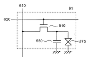
- the display device of one embodiment of the present invention can include a pixel portion 30, a circuit 40, and a circuit 60 as illustrated in FIG.
- the pixel portion 30, the circuit 40, the circuit 60, and the circuit 65 can be used.
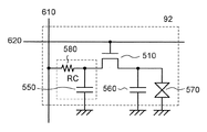
- FIG. 3 illustrates a pixel circuit 92 of one embodiment of the present invention.
- the pixel circuit 92 can be used as the pixel circuit 90 of the display device illustrated in FIG.
- one of the source and the drain of the transistor 510 is electrically connected to one electrode of the resistor 580 and one electrode of the capacitor 550.
- the other electrode of the resistance element 580 is electrically connected to the signal line 610.
- the other of the source and the drain of the transistor 510 is electrically connected to one electrode of the liquid crystal element 570 and one electrode of the capacitor 560.
- the gate of the transistor 510 is electrically connected to the scan line 620.
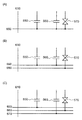
- the transistor 530 may be provided between the other of the source and the drain of the transistor 510 and one electrode of the capacitor 550 as illustrated in FIG.
- an on signal is supplied to the wiring 640 to turn on the transistor 520, so that the capacitor 550 and the resistor 580
- An RC circuit consisting of In the case where an operation for gradually changing the gradation is not necessary (second mode), the transistor 530 may be turned off. By turning off the transistor 530, the capacitor 550 can be prevented from being charged to the signal line 610 by a signal potential, and the response speed of the pixel can be improved.
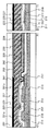
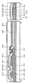
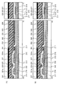
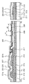
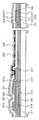
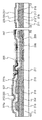
- the transistor 510 includes a conductive layer 875 having a function as a gate electrode provided over a substrate 810, an insulating layer 860 having a function as a gate insulating film, a semiconductor layer 830 having a function as an active layer, a source electrode Alternatively, the conductive layer 840 functions as one of the drain electrodes and the conductive layer 850 functions as the other of the source electrode and the drain electrode. Further, the protective film 870 and the protective film 880 can be provided over the transistor 510.
- the resistance layer 831 can be an oxide layer formed using the same process as the semiconductor layer 830.
- the resistance layer 831 can be an oxide layer containing impurities at the same level as the semiconductor layer 830, and can be an oxide in which impurities such as hydrogen are diffused from the protective film 880. It can be a physical layer.
- an In—Ga—Zn oxide can be used for the semiconductor layer 830 and the resistance layer 831.
- a silicon nitride film containing hydrogen can be used as the protective film 880.
- the resistance layer 831 can be a semiconductor layer formed using the same process as the semiconductor layer 830.
- the resistance layer 831 can be a silicon layer containing the same amount of impurities as the semiconductor layer 830, and can be a silicon layer in which phosphorus, boron, or the like is added to the semiconductor layer 830. be able to.
- the semiconductor layer 830 and the resistance layer 831 can be formed using an amorphous silicon layer, a polycrystalline silicon layer, or a single crystal silicon layer. Needless to say, the resistance layer 831 and the semiconductor layer 830 may be formed using different materials and different processes.
- the pixel portion 271, the scan line driver circuit 274, and the signal line driver circuit 276 are arranged in parallel or substantially in parallel, and the potential is controlled by the scan line driver circuit 274.
- the pixel portion 271 includes a plurality of pixels 270 arranged in a matrix. Further, along the signal line 279, there are common lines 275 arranged in parallel or substantially in parallel.
- the scanning line driver circuit 274 and the signal line driver circuit 276 are collectively referred to as a driver circuit portion.
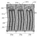
- the common electrode 229 has a striped region extending in a direction intersecting with the signal line.
- the striped region is connected to a region extending in a direction parallel or substantially parallel to the signal line. Therefore, in the plurality of pixels included in the display device 200, each region of the common electrode 229 having a striped region has the same potential.
- Display elements include, for example, liquid crystal elements, EL (electroluminescence) elements including LEDs (white LEDs, red LEDs, green LEDs, blue LEDs, etc.) (EL elements including organic substances and inorganic substances, organic EL elements, inorganic EL elements).
- EL electroluminescence
- LEDs white LEDs, red LEDs, green LEDs, blue LEDs, etc.
- EL elements including organic substances and inorganic substances, organic EL elements, inorganic EL elements).
- a silicon oxide film, a silicon oxynitride film, a silicon nitride oxide film, a silicon nitride film can be formed by a plasma CVD (CVD: Chemical Vapor Deposition) method, a sputtering method, or the like.
- Insulating films including one or more of aluminum oxide film, hafnium oxide film, yttrium oxide film, zirconium oxide film, gallium oxide film, tantalum oxide film, magnesium oxide film, lanthanum oxide film, cerium oxide film, and neodymium oxide film are used. be able to. Note that a single-layer insulating film selected from the above materials may be used instead of the stacked structure of the insulating films 215 and 217.
- the resistivity of the conductive film 220 is preferably 1 ⁇ 10 ⁇ 8 times or more and less than 1 ⁇ 10 ⁇ 1 times the resistivity of the semiconductor film 219, typically 1 ⁇ 10 ⁇ 3 ⁇ cm or more and 1 ⁇ .
- the resistivity is preferably less than 10 4 ⁇ cm, more preferably 1 ⁇ 10 ⁇ 3 ⁇ cm or more and less than 1 ⁇ 10 ⁇ 1 ⁇ cm.
- insulating films 223, 225, and 227 functioning as protective insulating films of the transistor 252
- a silicon oxide film, a silicon oxynitride film, a silicon nitride oxide film, a silicon nitride film, an aluminum oxide film, and the like are formed by a plasma CVD method, a sputtering method, or the like.
- An insulating film containing at least one of a hafnium oxide film, an yttrium oxide film, a zirconium oxide film, a gallium oxide film, a tantalum oxide film, a magnesium oxide film, a lanthanum oxide film, a cerium oxide film, and a neodymium oxide film can be used.
- a silicon oxynitride film that emits less nitrogen oxide is a film that releases more ammonia than nitrogen oxide in a temperature programmed desorption gas analysis method, and typically releases ammonia molecules.
- the amount is 1 ⁇ 10 18 molecules / cm 3 or more and 5 ⁇ 10 19 molecules / cm 3 or less.
- the amount of ammonia released is the amount released by heat treatment at a film surface temperature of 50 ° C. to 650 ° C., preferably 50 ° C. to 550 ° C.
- Nitrogen oxide typically NO 2 or NO forms a level in the insulating film 223 or the like.
- the level is located in the energy gap of the semiconductor film 219. Therefore, when nitrogen oxide diffuses to the interface between the insulating film 223 and the semiconductor film 219, the level may trap electrons on the insulating film 223 side. As a result, trapped electrons remain in the vicinity of the interface between the insulating film 223 and the semiconductor film 219, and thus the threshold voltage of the transistor is shifted in the positive direction.
- a third signal of .966 or less corresponds to a signal caused by nitrogen oxides (NO x , x is 0 or more and 2 or less, preferably 1 or more and 2 or less).
- nitrogen oxides include nitrogen monoxide and nitrogen dioxide. That is, a first signal having a g value of 2.037 to 2.039, a second signal having a g value of 2.001 to 2.003, and a first signal having a g value of 1.964 to 1.966. It can be said that the smaller the total density of the signal spins of 3, the smaller the content of nitrogen oxide contained in the oxide insulating film.
- the oxide insulating film in which the level density of nitrogen oxide is low between E v — os and E c — os has a nitrogen concentration measured by SIMS of 6 ⁇ 10 20 atoms / cm 3 or less.
- An oxide insulating film with a low nitrogen oxide level density is formed between Ev_os and Ec_os by using a PECVD method with a substrate temperature of 220 ° C. or higher and 350 ° C. or lower and using silane and dinitrogen monoxide. By doing so, a dense and high hardness film can be formed.
- the insulating film 225 preferably has a small amount of defects.
- the thickness of the insulating film 223 can be 5 nm to 150 nm, preferably 5 nm to 50 nm, preferably 10 nm to 30 nm.
- the thickness of the insulating film 225 can be greater than or equal to 30 nm and less than or equal to 500 nm, preferably greater than or equal to 150 nm and less than or equal to 400 nm.
- the insulating film 227 has a function of blocking oxygen, hydrogen, water, alkali metal, alkaline earth metal, and the like.
- diffusion of oxygen from the semiconductor film 219 to the outside, diffusion of oxygen contained in the insulating films 223 and 225, and entry of hydrogen, water, and the like into the semiconductor film 219 from the outside Can be prevented.
- an oxide insulating film having a blocking effect of oxygen, hydrogen, water, or the like may be provided instead of the nitride insulating film having a blocking effect of oxygen, hydrogen, water, alkali metal, alkaline earth metal, or the like.
- FIG. 31A is a schematic top view of the display device 300.
- FIG. FIG. 28B is a schematic cross-sectional view taken along the cutting line A1-A2, between A3-A4, and between A5-A6 in FIG. Note that some components are not illustrated in FIG. 28A for the sake of clarity.
- the display device 300 includes a display portion 302, a signal line driver circuit 303, a scanning line driver circuit 304, and an external connection terminal 305 on the upper surface of the substrate 301.
- the pixel has at least one switching transistor 312 and a storage capacitor (not shown).
- a comb-shaped first electrode 343 and a comb-shaped second electrode 352 which are electrically connected to one of a source electrode and a drain electrode of the transistor 312 and a comb-shaped second electrode 352 are provided over the insulating layer 342.
- a light-transmitting conductive material is used for at least one of the first electrode 343 and the second electrode 352. It is preferable to use a light-transmitting conductive material for both of these electrodes because the aperture ratio of the pixel can be increased.
- the color filter 327 is provided so as to overlap with the first electrode 343 and the second electrode 352.
- the light shielding layer 328 is provided so as to cover the side surface of the color filter 327.
- FIG. 28B illustrates a structure in which the color filter 327 is provided over the substrate 321, but the arrangement of the color filter is not limited to this position.
- a liquid crystal 353 is provided between the substrate 301 and the substrate 321.
- an electric field is generated in a substantially lateral direction, and the orientation of the liquid crystal 353 is controlled by the electric field, and the backlight is arranged outside the display device.
- An image can be displayed by controlling the polarization of the light from each pixel.
- An alignment film for controlling the alignment of the liquid crystal 353 is preferably provided on a surface in contact with the liquid crystal 353.
- a light-transmitting material is used for the alignment film.
- a polarizing plate is provided on the outer surface of the substrate 321 and the substrate 301 when viewed from the liquid crystal element 314.
- thermotropic liquid crystal a low-molecular liquid crystal, a polymer liquid crystal, a ferroelectric liquid crystal, an antiferroelectric liquid crystal, or the like can be used.
- a liquid crystal exhibiting a blue phase because an alignment film is unnecessary and a wide viewing angle can be obtained.
- liquid crystal 353 a material with high viscosity and low fluidity is preferably used for the liquid crystal 353.
- the liquid crystal element 314 to which the IPS mode is applied will be described.
- the configuration of the liquid crystal element is not limited to this, and other configurations include a TN (Twisted Nematic) mode, an FFS (Fringe Field Switching) mode, an ASM ( Axial Symmetrical Aligned Micro-cell) mode, OCB (Optically Compensated Birefringence) mode, FLC (Ferroelectric Liquid Crystal) mode, AFLC (Anti-FrequentialLiquid) mode can be used.
- TN Transmission Nematic
- FFS Fe Field Switching
- ASM Axial Symmetrical Aligned Micro-cell
- OCB Optically Compensated Birefringence
- FLC Fluorroelectric Liquid Crystal
- AFLC Anti-FrequentialLiquid
- Transistors (the transistor 311, the transistor 312, and the like) provided in the display device 300 are top-gate transistors.
- Each transistor includes a semiconductor layer 335, an insulating layer 334 functioning as a gate insulating layer, and a gate electrode 333.
- An insulating layer 338 and an insulating layer 339 which cover the gate electrode 333 are stacked, and the semiconductor layer 335 includes a pair of electrodes 336 through openings provided in the insulating layer 334, the insulating layer 338, and the insulating layer 339.
- an oxide semiconductor can be used for the semiconductor layer 335.
- the oxide semiconductor for example, the oxide semiconductor exemplified in the above embodiment can be used.
- the semiconductor layer 335 may include a source region or a region functioning as a drain region whose resistance is lower than that of a region functioning as a channel.
- the source region and the drain region can be provided in a portion in contact with the pair of electrodes 336 or can be provided with a region functioning as a channel interposed therebetween.
- a region whose resistivity is controlled by the method exemplified in the above embodiment may be used.
- silicon can be used for the semiconductor layer 335.
- a semiconductor device such as a transistor used for each driver circuit provided in the display device 300 is preferably made of silicon.
- amorphous silicon may be used as silicon, it is particularly preferable to use crystalline silicon.
- a top-gate transistor is preferably used.
- a material having low heat resistance can be used as a material for a wiring or an electrode above the semiconductor layer, so that a selection range of materials can be widened.
- the bottom gate structure exemplified in the above embodiment is used. This is preferable because the number of manufacturing steps can be reduced.
- active elements and nonlinear elements can be used as active elements (active elements and nonlinear elements).
- MIM Metal Insulator Metal
- TFD Thin Film Diode
- a passive matrix type that does not use an active element can be used. Since no active element (active element or non-linear element) is used, the number of manufacturing steps is small, so that manufacturing costs can be reduced or yield can be improved. Alternatively, since an active element (an active element or a non-linear element) is not used, an aperture ratio can be improved, power consumption can be reduced, or luminance can be increased.
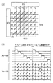
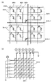
- the current detection circuit 602 is a circuit for detecting a change in current in the Y1-Y6 wiring due to a change in mutual capacitance in the capacitor 603.
- the wiring of Y1-Y6 there is no change in the current value detected when there is no proximity or contact with the detected object, but the current value when the mutual capacitance decreases due to the proximity or contact with the detected object. Detect changes that decrease.
- current detection may be performed using an integration circuit or the like.
- FIG. 29B shows a timing chart of input / output waveforms in the mutual capacitive touch sensor shown in FIG.
- the detection target is detected in each matrix in one frame period.
- FIG. 29B shows two cases, that is, a case where the detected object is not detected (non-touch) and a case where the detected object is detected (touch).
- the waveform made into the voltage value corresponding to the detected electric current value is shown.
- a transistor in which an oxide semiconductor is used for a semiconductor layer in which a channel is formed is preferably used.
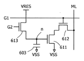
- the potential of the node n can be held for a long time, and the frequency of the operation (refresh operation) of supplying VRES to the node n can be reduced. it can.
- a configuration example of a touch panel in which a touch sensor is incorporated in a display unit having a plurality of pixels will be described.
- a liquid crystal element is used as a display element provided in a pixel.
- FIG. 31B is an equivalent circuit diagram illustrating a connection configuration of a plurality of wirings 3510 extending in the X direction and a plurality of wirings 3511 extending in the Y direction.
- An input voltage or a common potential can be input to each of the wirings 3510 extending in the X direction.
- a ground potential can be input to each of the wirings 3511 extending in the Y direction, or the wiring 3511 and the detection circuit can be electrically connected.
- the display device of one embodiment of the present invention can be used for the display panel 8006, for example.
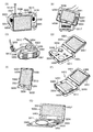
- a function of displaying a three-dimensional image, etc. by displaying the obtained image. Furthermore, in an electronic device having an image receiving unit, a function for capturing a still image, a function for capturing a moving image, a function for correcting a captured image automatically or manually, and a captured image on a recording medium (externally or incorporated in a camera) A function of saving, a function of displaying a photographed image on a display portion, and the like can be provided. Note that the functions of the electronic devices illustrated in FIGS. 34A to 34G are not limited to these, and the electronic devices can have various functions.
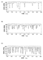
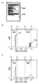
- FIG. 35 is a diagram for explaining the result of measuring the change in luminance in the region of the display device having a diameter of 100 ⁇ m.
- the text image was displayed while scrolling on the display device.
- the text image includes 49 characters of a size of 20 points per line and 25 lines per page.
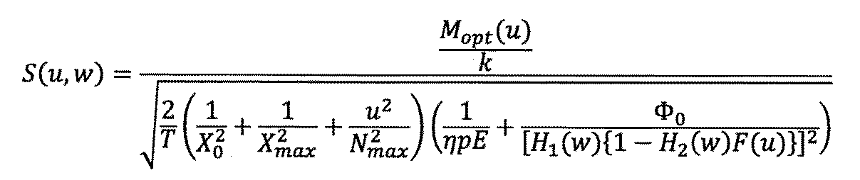
- k is the signal-to-noise ratio
- T is the visual integration time
- X 0 is the size of the object
- X max is the maximum integration region
- ⁇ is the quantum efficiency
- E is the retinal illuminance
- ⁇ 0 is the spectral density of the neural noise
- u 0 is the spatial frequency of side suppression.
- FIG. 36C is a diagram illustrating a result of calculating a change in visual stimulus based on a change in luminance illustrated in FIG. 35C using the Burton equation.
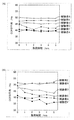
- FIG. 37 (A) is a diagram for explaining the results of measuring the critical fusion frequency (CCF) of six subjects who observed the text image explained using FIG. 35 (B).
- CCF critical fusion frequency
- the text image was displayed while scrolling using a Sharp Corporation make and model: AQUIOS PAD SH-06F.
- the pixel has a diagonal size of 7.0 inches, a resolution of 323 ppi, a liquid crystal element operating in a VA mode, and a transistor including an oxide semiconductor.
- the critical fusion frequency was measured using Shibata Kagaku Co., Ltd.'s Rigaku digital flicker value measuring instrument, model: RDF-1.
- FIG. 35B When the scrolling speed is fast, it is found that when the characters of the text image are displayed with bright gradation and the contrast is reduced, the change in luminance occurring in the same period is small and the visual stimulus is suppressed (FIG. 35B).
- CCF critical fusion frequency
Landscapes
- Physics & Mathematics (AREA)
- Engineering & Computer Science (AREA)
- Nonlinear Science (AREA)
- General Physics & Mathematics (AREA)
- Chemical & Material Sciences (AREA)
- Crystallography & Structural Chemistry (AREA)
- Mathematical Physics (AREA)
- Optics & Photonics (AREA)
- Microelectronics & Electronic Packaging (AREA)
- Theoretical Computer Science (AREA)
- General Engineering & Computer Science (AREA)
- Computer Hardware Design (AREA)
- Power Engineering (AREA)
- Human Computer Interaction (AREA)
- Liquid Crystal (AREA)
- Control Of Indicators Other Than Cathode Ray Tubes (AREA)
- Devices For Indicating Variable Information By Combining Individual Elements (AREA)
- Thin Film Transistor (AREA)
- Liquid Crystal Display Device Control (AREA)
- Electroluminescent Light Sources (AREA)
Abstract
Description
第1のモードが選択された場合は、視覚刺激が低減されるように、次に表示する画像情報を以下の方法を用いて表示する。
第2のモードが選択された場合は、以下の方法を用いて画像情報を表示する。例えば、画素回路に設けられた第1の機能を抑制するように、反転駆動を行わない駆動方式を設定する。または、画素回路の一部をバイパスする信号経路を用いて表示を行う。
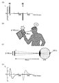
図38および図39を参照しながら、側抑制の影響を避ける表示方法について説明する。
刺激を受けた視神経の神経単位は、隣接する他の神経単位の活動を抑制する能力を備える。これにより、パルス状の視覚刺激に対する応答が変形する場合がある。
図40および図41を参照しながら、本発明の一態様を、本発明の一態様のプログラムを用いて説明する。
様々な命令に様々なイベントを関連付けることができる。
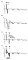
画像情報を表示する位置を、さまざまな速度で移動するスクロール命令の例を、図42を参照しながら説明する。なお、例えば、タッチパネルをスワイプする速度を用いて、スクロール命令の表示位置を移動する速度などを与えることができる。
時刻T1から時刻T2にかけて、画像情報を表示する位置を移動する速度を、0からV1まで加速するスクロール命令の例を説明する(図42(A−1)および図42(A−2)参照)。
時刻T3から時刻T4にかけて、画像情報を表示する位置を移動する速度を、V1から0まで減速するスクロール命令の例を説明する(図42(B−1)および図42(B−2)参照)。
時刻T6から時刻T7にかけて、画像情報を表示する位置を移動する速度を0からV1まで加速しながら移動し、時刻T7から時刻T8まで速度V1で移動する。また、時刻T8から時刻T9にかけて、画像情報を表示する位置を速度V1からV2まで減速しながら移動し、時刻T9以降は速度V2で移動するロール命令の例を説明する(図42(C−1)および図42(C−2)参照)。
次に表示する画像情報の特性をモードを選択する条件に用いる方法を、図43を参照しながら説明する。
例えば、次に表示する画像情報のコントラストが所定の値を超えるか否かを、第1のモードを選択する条件に用いることができる。
また、例えば、次に表示する画像情報に占める暗部の面積の割合を、モードを選択する条件に用いることができる。
本実施の形態では、本発明の一態様の表示装置について、図面を参照して説明する。本発明の一態様の表示装置は、図1(A)に示すように画素部30、回路40および回路60を有する構成とすることができる。または、図1(B)に示すように、画素部30、回路40、回路60および回路65を有する構成とすることもできる。
本実施の形態では、本発明の一態様の表示装置の具体的な構成について、図面を参照して説明する。
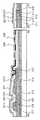
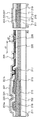
次に、表示装置200に含まれる画素の具体的な構成について説明する。まず、FFSモードによって駆動する表示装置200が有する複数の画素270a、270b、270cの上面図を図10に示す。
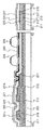
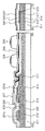
次に、表示装置200が有する、図10に示す画素とは異なる構成の複数の画素270d、270e、270fの上面図を図15に示す。
基板211の材質などに大きな制限はないが、少なくとも、後の熱処理に耐えうる程度の耐熱性を有している必要がある。例えば、ガラス基板、セラミック基板、石英基板、サファイア基板等を、基板211として用いてもよい。また、シリコンや炭化シリコンからなる単結晶半導体基板、多結晶半導体基板、シリコンゲルマニウム等の化合物半導体基板、SOI基板等を適用することも可能であり、これらの基板上に半導体素子が設けられたものを、基板211として用いてもよい。なお、基板211として、ガラス基板を用いる場合、第6世代(1500mm×1850mm)、第7世代(1870mm×2200mm)、第8世代(2200mm×2400mm)、第9世代(2400mm×2800mm)、第10世代(2950mm×3400mm)等の大面積基板を用いることで、大型の表示装置を作製することができる。また、基板211として、可撓性基板を用い、可撓性基板上に直接、トランジスタや容量素子等を形成してもよい。
トランジスタ252のゲート絶縁膜として機能する絶縁膜215、217としては、プラズマCVD(CVD:Chemical Vapor Deposition)法、スパッタリング法等により、酸化シリコン膜、酸化窒化シリコン膜、窒化酸化シリコン膜、窒化シリコン膜、酸化アルミニウム膜、酸化ハフニウム膜、酸化イットリウム膜、酸化ジルコニウム膜、酸化ガリウム膜、酸化タンタル膜、酸化マグネシウム膜、酸化ランタン膜、酸化セリウム膜および酸化ネオジム膜を一種以上含む絶縁膜を、それぞれ用いることができる。なお、絶縁膜215、217の積層構造とせずに、上述の材料から選択された単層の絶縁膜を用いてもよい。
ゲート電極として機能する導電膜213、ソース電極またはドレイン電極として機能する導電膜221a、221bに用いることのできる材料としては、アルミニウム、チタン、クロム、ニッケル、銅、イットリウム、ジルコニウム、モリブデン、銀、タンタル、またはタングステンからなる金属、またはこれを主成分とする合金を単層構造または積層構造として用いることができる。例えば、アルミニウム膜上にチタン膜を積層する二層構造、タングステン膜上にチタン膜を積層する二層構造、モリブデン膜上に銅膜を積層した二層構造、モリブデンとタングステンを含む合金膜上に銅膜を積層した二層構造、銅−マグネシウム−アルミニウム合金膜上に銅膜を積層する二層構造、チタン膜または窒化チタン膜と、そのチタン膜または窒化チタン膜上に重ねてアルミニウム膜または銅膜を積層し、さらにその上にチタン膜または窒化チタン膜を形成する三層構造、モリブデン膜または窒化モリブデン膜と、そのモリブデン膜または窒化モリブデン膜上に重ねてアルミニウム膜または銅膜を積層し、さらにその上にモリブデン膜または窒化モリブデン膜を形成する三層構造等がある。また、ソース電極またはドレイン電極として機能する導電膜221a、221bを三層構造とする場合、一層目及び三層目には、チタン、窒化チタン、モリブデン、タングステン、モリブデンとタングステンを含む合金、モリブデンとジルコニウムを含む合金、又は窒化モリブデンでなる膜を形成し、2層目には、銅、アルミニウム、金又は銀、或いは銅とマンガンの合金等の低抵抗材料でなる膜を形成することが好ましい。なお、インジウム錫酸化物、酸化タングステンを含むインジウム酸化物、酸化タングステンを含むインジウム亜鉛酸化物、酸化チタンを含むインジウム酸化物、酸化チタンを含むインジウム錫酸化物、インジウム亜鉛酸化物、酸化シリコンを添加したインジウム錫酸化物等の透光性を有する導電性材料を用いてもよい。また、導電膜213、ソース電極またはドレイン電極として機能する導電膜221a、221bに用いることのできる材料は、例えば、スパッタリング法を用いて形成することができる。
コモン電極229として機能する導電膜としては、例えば、可視光において、透光性を有する材料を用いればよい。具体的には、インジウム(In)、亜鉛(Zn)、錫(Sn)の中から選ばれた一種を含む材料を用いるとよい。また、当該導電膜としては、例えば、酸化タングステンを含むインジウム酸化物、酸化タングステンを含むインジウム亜鉛酸化物、酸化チタンを含むインジウム酸化物、酸化チタンを含むインジウム錫酸化物、インジウム錫酸化物(ITO:Indium Tin Oxide)、インジウム亜鉛酸化物、酸化ケイ素を添加したインジウム錫酸化物などの透光性を有する導電性材料を用いることができる。また、当該導電膜としては、例えば、スパッタリング法を用いて形成することができる。
半導体膜219及び導電膜220に用いることのできる酸化物半導体膜は、膜中の酸素欠損及び/又は膜中の水素、水等の不純物濃度によって、抵抗率を制御することができる半導体材料である。そのため、半導体膜219及び導電膜220へ酸素欠損及び/又は不純物濃度が増加する処理、または酸素欠損及び/又は不純物濃度が低減する処理を選択することによって、それぞれの酸化物半導体膜の抵抗率を制御することができる。
トランジスタ252の保護絶縁膜として機能する絶縁膜223、225、227としては、プラズマCVD法、スパッタリング法等により、酸化シリコン膜、酸化窒化シリコン膜、窒化酸化シリコン膜、窒化シリコン膜、酸化アルミニウム膜、酸化ハフニウム膜、酸化イットリウム膜、酸化ジルコニウム膜、酸化ガリウム膜、酸化タンタル膜、酸化マグネシウム膜、酸化ランタン膜、酸化セリウム膜および酸化ネオジム膜を一種以上含む絶縁膜を、それぞれ用いることができる。
本実施の形態では、上記実施の形態で例示した表示システムに適用可能な表示装置の他の構成例について説明する。
本実施の形態では、本発明の一態様の入力装置、または入出力装置の駆動方法の例について、図面を参照して説明する。
図29(A)は、相互容量方式のタッチセンサの構成を示すブロック図である。図29(A)では、パルス電圧出力回路601、電流検出回路602を示している。なお図29(A)では、パルス電圧が与えられる電極621、電流の変化を検知する電極622をそれぞれ、X1−X6、Y1−Y6のそれぞれ6本の配線として示している。また図29(A)は、電極621および電極622が重畳することで形成される容量603を図示している。なお、電極621と電極622とはその機能を互いに置き換えてもよい。
上記では、タッチセンサを構成する電極を、表示素子等が設けられる基板とは異なる基板上に形成した場合を示したが、表示素子等が設けられる基板上に、タッチセンサを構成する一対の電極のいずれか一方、または両方を設ける構成としてもよい。
本実施の形態では、本発明の一態様の表示装置を有する表示モジュール及び電子機器について、図33及び図34を用いて説明を行う。
スクロールの速度が遅い場合、スクロールの速度が速い場合に比べて、同じ期間に生じる輝度の変化が少なく、視覚刺激が抑制されることが分かった(図35(A)、図35(C)、図36(A)および図36(C)参照)。
40 回路
50 画素回路
60 回路
65 回路
70 液晶素子
81 容量素子
90 画素回路
91 画素回路
92 画素回路
93 画素回路
94 画素回路
95 画素回路
100 直径
200 表示装置
211 基板
213 導電膜
215 絶縁膜
217 絶縁膜
219 半導体膜
219a 半導体膜
220 導電膜
221a 導電膜
221b 導電膜
223 絶縁膜
225 絶縁膜
227 絶縁膜
228 絶縁膜
229 コモン電極
243 導電膜
245 絶縁膜
247 導電膜
250 液晶層
251 基板
252 トランジスタ
255 容量素子
258 抵抗素子
261 遮光膜
262 着色膜
270 画素
270a 画素
270b 画素
270c 画素
270d 画素
270e 画素
270f 画素
271 画素部
274 走査線駆動回路
275 コモン線
276 信号線駆動回路
277 走査線
279 信号線
300 表示装置
301 基板
302 表示部
303 信号線駆動回路
304 走査線駆動回路
305 外部接続端子
311 トランジスタ
312 トランジスタ
314 液晶素子
321 基板
327 カラーフィルタ
328 遮光層
332 絶縁層
333 ゲート電極
334 絶縁層
335 半導体層
336 電極
338 絶縁層
339 絶縁層
341 絶縁層
342 絶縁層
343 電極
352 電極
353 液晶
510 トランジスタ
520 トランジスタ
530 トランジスタ
550 容量素子
560 容量素子
570 液晶素子
580 抵抗素子
601 パルス電圧出力回路
602 電流検出回路
603 容量
610 信号線
611 トランジスタ
612 トランジスタ
613 トランジスタ
620 走査線
621 電極
622 電極
630 走査線
640 配線
650 配線
660 配線
670 配線
810 基板
830 半導体層
831 抵抗層
840 導電層
850 導電層
855 導電層
860 絶縁層
870 保護膜
875 導電層
880 保護膜
920 走査線
3501 配線
3502 配線
3503 トランジスタ
3504 液晶素子
3510 配線
3510_1 配線
3510_2 配線
3511 配線
3515_1 ブロック
3515_2 ブロック
3516 ブロック
5000 筐体
5001 表示部
5002 表示部
5003 スピーカ
5004 LEDランプ
5005 操作キー
5006 接続端子
5007 センサ
5008 マイクロフォン
5009 スイッチ
5010 赤外線ポート
5011 記録媒体読込部
5012 支持部
5013 イヤホン
5014 アンテナ
5015 シャッターボタン
5016 受像部
5017 充電器
8000 表示モジュール
8001 上部カバー
8002 下部カバー
8003 FPC
8004 タッチパネル
8005 FPC
8006 表示パネル
8007 バックライト
8008 光源
8009 フレーム
8010 プリント基板
8011 バッテリ
Claims (8)
- トランジスタと、抵抗素子と、第1の容量素子と、第2の容量素子と、液晶素子と、を有する表示装置であって、
前記トランジスタのソースまたはドレインの一方は、前記抵抗素子の一方の電極と電気的に接続され、
前記トランジスタのソースまたはドレインの一方は、前記第1の容量素子の一方の電極と接続され、
前記抵抗素子の他方の電極は、第1の配線と電気的に接続され、
前記トランジスタのソースまたはドレインの他方は、前記液晶素子の一方の電極と電気的に接続され、
前記トランジスタのソースまたはドレインの他方は、前記第2の容量素子の一方の電極と接続され、
前記トランジスタのゲートは第2の配線に電気的に接続される表示装置。 - 請求項1において、
前記トランジスタは、チャネルが形成される領域に酸化物半導体を有する表示装置。 - 第1のトランジスタと、第2のトランジスタと、抵抗素子と、第1の容量素子と、第2の容量素子と、液晶素子と、を有する表示装置であって、
前記第1のトランジスタのソースまたはドレインの一方は、前記抵抗素子の一方の電極と電気的に接続され、
前記第1のトランジスタのソースまたはドレインの一方は、前記第1の容量素子の一方の電極と接続され、
前記抵抗素子の他方の電極は、第1の配線と電気的に接続され、
前記第1のトランジスタのソースまたはドレインの他方は、前記液晶素子の一方の電極と電気的に接続され、
前記第1のトランジスタのソースまたはドレインの他方は、前記第2の容量素子の一方の電極と接続され、
前記第1のトランジスタのゲートは第2の配線に電気的に接続され、
前記第2のトランジスタのソースまたはドレインの一方は、前記抵抗素子の他方の電極と電気的に接続され、
前記第2のトランジスタのソースまたはドレインの他方は、前記第1のトランジスタのソースまたはドレインの他方と電気的に接続され。
前記第2のトランジスタのゲートは、第3の配線に電気的に接続されている表示装置。 - 第1のトランジスタと、第2のトランジスタと、抵抗素子と、第1の容量素子と、第2の容量素子と、液晶素子と、を有する表示装置であって、
前記第1のトランジスタのソースまたはドレインの一方は、第1の配線に電気的に接続され、
前記第1のトランジスタのソースまたはドレインの他方は、前記第1の容量素子の一方の電極と電気的に接続され、
前記第1のトランジスタのソースまたはドレインの他方は、前記抵抗素子の一方の電極と電気的に接続され、
前記抵抗素子の他方の電極は、前記第2の容量素子の一方電極と電気的に接続され、
前記抵抗素子の他方の電極は、前記液晶素子の一方の電極と電気的に接続され、
前記第1のトランジスタのゲートは、第2の配線と電気的に接続され、
前記第2のトランジスタのソースまたはドレインの一方は、前記抵抗素子の一方の電極と電気的に接続され、
前記第2のトランジスタのソースまたはドレインの他方は、前記抵抗素子の他方の電極と電気的に接続され、
前記第2のトランジスタのゲートは、第3の配線と電気的に接続されている表示装置。 - 請求項3または4において、
前記第1のトランジスタおよび前記第2のトランジスタは、チャネルが形成される領域に酸化物半導体を有する表示装置。 - 請求項3または4において、
前記抵抗素子の抵抗層は、酸化物である表示装置。 - 請求項3または4において、
前記液晶素子にて表示される画像を第1の速度以上でスクロールしたときには、前記第2のトランジスタを介さずに前記液晶素子に画像信号が供給され、
前記液晶素子にて表示される画像を前記第1の速度より小さい第2の速度でスクロールしたときには、前記第2のトランジスタを介して前記液晶素子に画像信号が供給される表示装置。 - 請求項1、3、4のいずれか一項に記載の表示装置と、
スピーカと、
マイクロフォンと、
を有する電子機器。
Priority Applications (2)
| Application Number | Priority Date | Filing Date | Title |
|---|---|---|---|
| US15/552,818 US10379414B2 (en) | 2015-03-03 | 2016-02-23 | Display device comprising a transistor electrically connected to a resistor and a first capacitor and electronic device having the same |
| JP2017503201A JP6630720B2 (ja) | 2015-03-03 | 2016-02-23 | 表示装置 |
Applications Claiming Priority (4)
| Application Number | Priority Date | Filing Date | Title |
|---|---|---|---|
| JP2015040975 | 2015-03-03 | ||
| JP2015040962 | 2015-03-03 | ||
| JP2015-040962 | 2015-03-03 | ||
| JP2015-040975 | 2015-03-03 |
Publications (1)
| Publication Number | Publication Date |
|---|---|
| WO2016139549A1 true WO2016139549A1 (ja) | 2016-09-09 |
Family
ID=56849210
Family Applications (1)
| Application Number | Title | Priority Date | Filing Date |
|---|---|---|---|
| PCT/IB2016/050948 Ceased WO2016139549A1 (ja) | 2015-03-03 | 2016-02-23 | 表示装置および電子機器 |
Country Status (3)
| Country | Link |
|---|---|
| US (1) | US10379414B2 (ja) |
| JP (2) | JP6630720B2 (ja) |
| WO (1) | WO2016139549A1 (ja) |
Cited By (1)
| Publication number | Priority date | Publication date | Assignee | Title |
|---|---|---|---|---|
| CN115083364A (zh) * | 2022-06-23 | 2022-09-20 | 惠科股份有限公司 | 像素电路、阵列基板及显示面板 |
Families Citing this family (11)
| Publication number | Priority date | Publication date | Assignee | Title |
|---|---|---|---|---|
| CN104760402B (zh) * | 2015-04-09 | 2018-04-20 | 京东方科技集团股份有限公司 | 用于三维打印机的曝光装置、三维打印机和三维打印方法 |
| US10483285B2 (en) * | 2016-06-01 | 2019-11-19 | Innolux Corporation | Element substrate and display device |
| KR102686294B1 (ko) * | 2016-12-23 | 2024-07-22 | 삼성디스플레이 주식회사 | 조향 핸들 및 이를 포함하는 차량 제어 시스템 |
| US20180323239A1 (en) * | 2017-05-03 | 2018-11-08 | Innolux Corporation | Display device |
| CN107589575A (zh) * | 2017-09-30 | 2018-01-16 | 联想(北京)有限公司 | 显示屏 |
| CN112334867B (zh) | 2018-05-24 | 2025-11-11 | 纽约州立大学研究基金会 | 电容传感器 |
| GB2610886B (en) | 2019-08-21 | 2023-09-13 | Pragmatic Printing Ltd | Resistor geometry |
| GB2587793B (en) * | 2019-08-21 | 2023-03-22 | Pragmatic Printing Ltd | Electronic circuit comprising transistor and resistor |
| KR102831677B1 (ko) * | 2020-01-09 | 2025-07-09 | 삼성디스플레이 주식회사 | 표시 장치 및 표시 장치의 제조 방법 |
| CN114999369B (zh) * | 2022-06-08 | 2023-08-04 | 滁州惠科光电科技有限公司 | 像素驱动电路及显示面板 |
| CN119626177B (zh) * | 2024-12-20 | 2025-10-28 | 惠州华阳通用电子有限公司 | 一种显示屏电源驱动装置及方法 |
Citations (2)
| Publication number | Priority date | Publication date | Assignee | Title |
|---|---|---|---|---|
| JP2003255305A (ja) * | 2002-02-27 | 2003-09-10 | Fujitsu Display Technologies Corp | 液晶表示装置及びその駆動方法 |
| JP2008287032A (ja) * | 2007-05-17 | 2008-11-27 | Semiconductor Energy Lab Co Ltd | 液晶表示装置 |
Family Cites Families (17)
| Publication number | Priority date | Publication date | Assignee | Title |
|---|---|---|---|---|
| US6337722B1 (en) * | 1997-08-07 | 2002-01-08 | Lg.Philips Lcd Co., Ltd | Liquid crystal display panel having electrostatic discharge prevention circuitry |
| JP2003047636A (ja) | 2001-05-28 | 2003-02-18 | Nikon Corp | 眼疲労解消装置 |
| JP4269542B2 (ja) * | 2001-06-04 | 2009-05-27 | 日本電気株式会社 | トランジスタの動作点設定方法及びその回路、信号成分値変更方法並びにアクティブマトリクス型液晶表示装置 |
| TWI230915B (en) * | 2003-10-16 | 2005-04-11 | Ind Tech Res Inst | Driving circuit of optical modulator |
| JP5116277B2 (ja) * | 2006-09-29 | 2013-01-09 | 株式会社半導体エネルギー研究所 | 半導体装置、表示装置、液晶表示装置、表示モジュール及び電子機器 |
| JP5542296B2 (ja) * | 2007-05-17 | 2014-07-09 | 株式会社半導体エネルギー研究所 | 液晶表示装置、表示モジュール及び電子機器 |
| JP4989309B2 (ja) * | 2007-05-18 | 2012-08-01 | 株式会社半導体エネルギー研究所 | 液晶表示装置 |
| JP4927029B2 (ja) | 2007-05-30 | 2012-05-09 | 京セラ株式会社 | 携帯電子機器及び携帯電子機器における文字表示方法 |
| US8487936B2 (en) | 2007-05-30 | 2013-07-16 | Kyocera Corporation | Portable electronic device and character display method for the same |
| KR101746198B1 (ko) | 2009-09-04 | 2017-06-12 | 가부시키가이샤 한도오따이 에네루기 켄큐쇼 | 표시장치 및 전자기기 |
| US8837203B2 (en) | 2011-05-19 | 2014-09-16 | Semiconductor Energy Laboratory Co., Ltd. | Semiconductor device |
| CN102789808B (zh) | 2011-05-20 | 2018-03-06 | 株式会社半导体能源研究所 | 存储器装置和用于驱动存储器装置的方法 |
| US8878589B2 (en) | 2011-06-30 | 2014-11-04 | Semiconductor Energy Laboratory Co., Ltd. | Semiconductor device and driving method thereof |
| KR101941984B1 (ko) * | 2011-09-27 | 2019-04-12 | 삼성디스플레이 주식회사 | 액정표시장치 |
| US9594281B2 (en) * | 2012-11-30 | 2017-03-14 | Semiconductor Energy Laboratory Co., Ltd. | Liquid crystal display device |
| KR102315811B1 (ko) * | 2015-02-16 | 2021-10-25 | 삼성디스플레이 주식회사 | 표시 장치 |
| CN105469754B (zh) * | 2015-12-04 | 2017-12-01 | 武汉华星光电技术有限公司 | 降低馈通电压的goa电路 |
-
2016
- 2016-02-23 WO PCT/IB2016/050948 patent/WO2016139549A1/ja not_active Ceased
- 2016-02-23 JP JP2017503201A patent/JP6630720B2/ja not_active Expired - Fee Related
- 2016-02-23 US US15/552,818 patent/US10379414B2/en not_active Expired - Fee Related
-
2019
- 2019-12-09 JP JP2019221851A patent/JP2020065059A/ja not_active Withdrawn
Patent Citations (2)
| Publication number | Priority date | Publication date | Assignee | Title |
|---|---|---|---|---|
| JP2003255305A (ja) * | 2002-02-27 | 2003-09-10 | Fujitsu Display Technologies Corp | 液晶表示装置及びその駆動方法 |
| JP2008287032A (ja) * | 2007-05-17 | 2008-11-27 | Semiconductor Energy Lab Co Ltd | 液晶表示装置 |
Cited By (2)
| Publication number | Priority date | Publication date | Assignee | Title |
|---|---|---|---|---|
| CN115083364A (zh) * | 2022-06-23 | 2022-09-20 | 惠科股份有限公司 | 像素电路、阵列基板及显示面板 |
| CN115083364B (zh) * | 2022-06-23 | 2023-06-30 | 惠科股份有限公司 | 像素电路、阵列基板及显示面板 |
Also Published As
| Publication number | Publication date |
|---|---|
| JP2020065059A (ja) | 2020-04-23 |
| US10379414B2 (en) | 2019-08-13 |
| US20180046004A1 (en) | 2018-02-15 |
| JP6630720B2 (ja) | 2020-01-15 |
| JPWO2016139549A1 (ja) | 2018-01-11 |
Similar Documents
| Publication | Publication Date | Title |
|---|---|---|
| JP6630720B2 (ja) | 表示装置 | |
| JP7781324B2 (ja) | 半導体装置の作成方法 | |
| JP7223807B2 (ja) | 液晶表示装置 | |
| US9851839B2 (en) | Display system | |
| US11048111B2 (en) | Display device equipped touch panel | |
| US10706790B2 (en) | Display device, display module including the display device, and electronic device including the display device or the display module | |
| US9818880B2 (en) | Semiconductor device and display device including the semiconductor device | |
| US20150255029A1 (en) | Display device, display module including the display device, and electronic device including the display device or the display module | |
| JP2017211638A (ja) | 表示装置、モジュール、及び電子機器 | |
| JP2025061317A (ja) | タッチパネル | |
| US20140152685A1 (en) | Semiconductor device and program | |
| TW201724194A (zh) | 半導體裝置的製造方法 | |
| JP7807609B1 (ja) | 表示装置 | |
| US20220013545A1 (en) | Semiconductor device, display device, and electronic device using the display device | |
| US20140184968A1 (en) | Liquid crystal display device | |
| JP2016173566A (ja) | 表示装置、表示モジュール、及び電子機器 | |
| JPWO2017006202A1 (ja) | 液晶表示装置および電子機器 | |
| JP2016167056A (ja) | 情報処理装置の駆動方法、プログラム、及び情報処理装置 | |
| JP6764663B2 (ja) | 情報処理装置 | |
| WO2017109642A1 (ja) | 金属酸化物膜、および半導体装置 |
Legal Events
| Date | Code | Title | Description |
|---|---|---|---|
| 121 | Ep: the epo has been informed by wipo that ep was designated in this application |
Ref document number: 16758519 Country of ref document: EP Kind code of ref document: A1 |
|
| ENP | Entry into the national phase |
Ref document number: 2017503201 Country of ref document: JP Kind code of ref document: A |
|
| WWE | Wipo information: entry into national phase |
Ref document number: 15552818 Country of ref document: US |
|
| NENP | Non-entry into the national phase |
Ref country code: DE |
|
| 122 | Ep: pct application non-entry in european phase |
Ref document number: 16758519 Country of ref document: EP Kind code of ref document: A1 |