WO2016117526A1 - 画像表示装置の製造方法、それに用いる硬化性樹脂組成物、タッチパネル及び画像表示装置 - Google Patents
画像表示装置の製造方法、それに用いる硬化性樹脂組成物、タッチパネル及び画像表示装置 Download PDFInfo
- Publication number
- WO2016117526A1 WO2016117526A1 PCT/JP2016/051357 JP2016051357W WO2016117526A1 WO 2016117526 A1 WO2016117526 A1 WO 2016117526A1 JP 2016051357 W JP2016051357 W JP 2016051357W WO 2016117526 A1 WO2016117526 A1 WO 2016117526A1
- Authority
- WO
- WIPO (PCT)
- Prior art keywords
- resin composition
- curable resin
- liquid crystal
- crystal display
- meth
- Prior art date
- Legal status (The legal status is an assumption and is not a legal conclusion. Google has not performed a legal analysis and makes no representation as to the accuracy of the status listed.)
- Ceased
Links
Images



Classifications
-
- C—CHEMISTRY; METALLURGY
- C09—DYES; PAINTS; POLISHES; NATURAL RESINS; ADHESIVES; COMPOSITIONS NOT OTHERWISE PROVIDED FOR; APPLICATIONS OF MATERIALS NOT OTHERWISE PROVIDED FOR
- C09J—ADHESIVES; NON-MECHANICAL ASPECTS OF ADHESIVE PROCESSES IN GENERAL; ADHESIVE PROCESSES NOT PROVIDED FOR ELSEWHERE; USE OF MATERIALS AS ADHESIVES
- C09J5/00—Adhesive processes in general; Adhesive processes not provided for elsewhere, e.g. relating to primers
-
- C—CHEMISTRY; METALLURGY
- C08—ORGANIC MACROMOLECULAR COMPOUNDS; THEIR PREPARATION OR CHEMICAL WORKING-UP; COMPOSITIONS BASED THEREON
- C08F—MACROMOLECULAR COMPOUNDS OBTAINED BY REACTIONS ONLY INVOLVING CARBON-TO-CARBON UNSATURATED BONDS
- C08F2/00—Processes of polymerisation
- C08F2/46—Polymerisation initiated by wave energy or particle radiation
- C08F2/48—Polymerisation initiated by wave energy or particle radiation by ultraviolet or visible light
- C08F2/50—Polymerisation initiated by wave energy or particle radiation by ultraviolet or visible light with sensitising agents
-
- C—CHEMISTRY; METALLURGY
- C08—ORGANIC MACROMOLECULAR COMPOUNDS; THEIR PREPARATION OR CHEMICAL WORKING-UP; COMPOSITIONS BASED THEREON
- C08F—MACROMOLECULAR COMPOUNDS OBTAINED BY REACTIONS ONLY INVOLVING CARBON-TO-CARBON UNSATURATED BONDS
- C08F20/00—Homopolymers and copolymers of compounds having one or more unsaturated aliphatic radicals, each having only one carbon-to-carbon double bond, and only one being terminated by only one carboxyl radical or a salt, anhydride, ester, amide, imide or nitrile thereof
- C08F20/02—Monocarboxylic acids having less than ten carbon atoms, Derivatives thereof
- C08F20/10—Esters
- C08F20/12—Esters of monohydric alcohols or phenols
- C08F20/16—Esters of monohydric alcohols or phenols of phenols or of alcohols containing two or more carbon atoms
- C08F20/18—Esters of monohydric alcohols or phenols of phenols or of alcohols containing two or more carbon atoms with acrylic or methacrylic acids
-
- C—CHEMISTRY; METALLURGY
- C09—DYES; PAINTS; POLISHES; NATURAL RESINS; ADHESIVES; COMPOSITIONS NOT OTHERWISE PROVIDED FOR; APPLICATIONS OF MATERIALS NOT OTHERWISE PROVIDED FOR
- C09J—ADHESIVES; NON-MECHANICAL ASPECTS OF ADHESIVE PROCESSES IN GENERAL; ADHESIVE PROCESSES NOT PROVIDED FOR ELSEWHERE; USE OF MATERIALS AS ADHESIVES
- C09J109/00—Adhesives based on homopolymers or copolymers of conjugated diene hydrocarbons
-
- C—CHEMISTRY; METALLURGY
- C09—DYES; PAINTS; POLISHES; NATURAL RESINS; ADHESIVES; COMPOSITIONS NOT OTHERWISE PROVIDED FOR; APPLICATIONS OF MATERIALS NOT OTHERWISE PROVIDED FOR
- C09J—ADHESIVES; NON-MECHANICAL ASPECTS OF ADHESIVE PROCESSES IN GENERAL; ADHESIVE PROCESSES NOT PROVIDED FOR ELSEWHERE; USE OF MATERIALS AS ADHESIVES
- C09J175/00—Adhesives based on polyureas or polyurethanes; Adhesives based on derivatives of such polymers
- C09J175/04—Polyurethanes
- C09J175/14—Polyurethanes having carbon-to-carbon unsaturated bonds
- C09J175/16—Polyurethanes having carbon-to-carbon unsaturated bonds having terminal carbon-to-carbon unsaturated bonds
-
- G—PHYSICS
- G02—OPTICS
- G02F—OPTICAL DEVICES OR ARRANGEMENTS FOR THE CONTROL OF LIGHT BY MODIFICATION OF THE OPTICAL PROPERTIES OF THE MEDIA OF THE ELEMENTS INVOLVED THEREIN; NON-LINEAR OPTICS; FREQUENCY-CHANGING OF LIGHT; OPTICAL LOGIC ELEMENTS; OPTICAL ANALOGUE/DIGITAL CONVERTERS
- G02F1/00—Devices or arrangements for the control of the intensity, colour, phase, polarisation or direction of light arriving from an independent light source, e.g. switching, gating or modulating; Non-linear optics
- G02F1/01—Devices or arrangements for the control of the intensity, colour, phase, polarisation or direction of light arriving from an independent light source, e.g. switching, gating or modulating; Non-linear optics for the control of the intensity, phase, polarisation or colour
- G02F1/13—Devices or arrangements for the control of the intensity, colour, phase, polarisation or direction of light arriving from an independent light source, e.g. switching, gating or modulating; Non-linear optics for the control of the intensity, phase, polarisation or colour based on liquid crystals, e.g. single liquid crystal display cells
- G02F1/133—Constructional arrangements; Operation of liquid crystal cells; Circuit arrangements
- G02F1/1333—Constructional arrangements; Manufacturing methods
-
- G—PHYSICS
- G06—COMPUTING OR CALCULATING; COUNTING
- G06F—ELECTRIC DIGITAL DATA PROCESSING
- G06F3/00—Input arrangements for transferring data to be processed into a form capable of being handled by the computer; Output arrangements for transferring data from processing unit to output unit, e.g. interface arrangements
- G06F3/01—Input arrangements or combined input and output arrangements for interaction between user and computer
- G06F3/03—Arrangements for converting the position or the displacement of a member into a coded form
- G06F3/041—Digitisers, e.g. for touch screens or touch pads, characterised by the transducing means
-
- G—PHYSICS
- G09—EDUCATION; CRYPTOGRAPHY; DISPLAY; ADVERTISING; SEALS
- G09F—DISPLAYING; ADVERTISING; SIGNS; LABELS OR NAME-PLATES; SEALS
- G09F9/00—Indicating arrangements for variable information in which the information is built-up on a support by selection or combination of individual elements
-
- C—CHEMISTRY; METALLURGY
- C09—DYES; PAINTS; POLISHES; NATURAL RESINS; ADHESIVES; COMPOSITIONS NOT OTHERWISE PROVIDED FOR; APPLICATIONS OF MATERIALS NOT OTHERWISE PROVIDED FOR
- C09J—ADHESIVES; NON-MECHANICAL ASPECTS OF ADHESIVE PROCESSES IN GENERAL; ADHESIVE PROCESSES NOT PROVIDED FOR ELSEWHERE; USE OF MATERIALS AS ADHESIVES
- C09J2203/00—Applications of adhesives in processes or use of adhesives in the form of films or foils
- C09J2203/318—Applications of adhesives in processes or use of adhesives in the form of films or foils for the production of liquid crystal displays
-
- C—CHEMISTRY; METALLURGY
- C09—DYES; PAINTS; POLISHES; NATURAL RESINS; ADHESIVES; COMPOSITIONS NOT OTHERWISE PROVIDED FOR; APPLICATIONS OF MATERIALS NOT OTHERWISE PROVIDED FOR
- C09J—ADHESIVES; NON-MECHANICAL ASPECTS OF ADHESIVE PROCESSES IN GENERAL; ADHESIVE PROCESSES NOT PROVIDED FOR ELSEWHERE; USE OF MATERIALS AS ADHESIVES
- C09J2301/00—Additional features of adhesives in the form of films or foils
- C09J2301/30—Additional features of adhesives in the form of films or foils characterized by the chemical, physicochemical or physical properties of the adhesive or the carrier
- C09J2301/312—Additional features of adhesives in the form of films or foils characterized by the chemical, physicochemical or physical properties of the adhesive or the carrier parameters being the characterizing feature
-
- C—CHEMISTRY; METALLURGY
- C09—DYES; PAINTS; POLISHES; NATURAL RESINS; ADHESIVES; COMPOSITIONS NOT OTHERWISE PROVIDED FOR; APPLICATIONS OF MATERIALS NOT OTHERWISE PROVIDED FOR
- C09J—ADHESIVES; NON-MECHANICAL ASPECTS OF ADHESIVE PROCESSES IN GENERAL; ADHESIVE PROCESSES NOT PROVIDED FOR ELSEWHERE; USE OF MATERIALS AS ADHESIVES
- C09J2301/00—Additional features of adhesives in the form of films or foils
- C09J2301/40—Additional features of adhesives in the form of films or foils characterized by the presence of essential components
- C09J2301/416—Additional features of adhesives in the form of films or foils characterized by the presence of essential components use of irradiation
Definitions
- the present invention relates to an image display device manufacturing method for manufacturing an image display device by bonding an optical substrate having a light-shielding portion and another optical substrate, a curable resin composition used therefor, a touch panel, and an image display device.
- a touch panel In recent years, display devices that allow screen input by attaching a touch panel to a display screen of a display device such as a liquid crystal display, a plasma display, or an organic EL display have been widely used.
- a glass plate or a resin film on which a transparent electrode is formed is bonded with a slight gap facing each other. If necessary, a transparent protection made of glass or resin is provided on the touch surface. It has a structure in which plates are bonded together.
- the present invention relates to a method for manufacturing an image display device capable of obtaining an image display device having excellent visibility without causing ripples when any part of the image display device is pressed, and a curable resin composition used therefor
- An object is to provide an object, a touch panel, and an image display device.
- the present invention relates to the following (1) to (14).
- a method of manufacturing an image display device in which a protective plate is bonded to a liquid crystal display unit The liquid crystal display unit fixes the liquid crystal display unit by surrounding a liquid crystal display cell, a polarizing plate disposed on the liquid crystal display cell, a sealing body that covers the liquid crystal display cell surrounding the polarizing plate, or a peripheral wall portion of the liquid crystal display cell.
- a method for manufacturing an image display device comprising the following steps (CI) to (C-III) after the step (B): (CI) First curable resin composition curing step for curing the first curable resin composition and bonding the liquid crystal display unit and the protective plate. (CII) Connecting the liquid crystal display unit and the protective plate.
- the average thickness of the coating film of the first curable resin composition is equal to or less than the average thickness of the coating film of the second curable resin composition, described in (1) or (2) Manufacturing method of the image display apparatus.
- the transparent plate is formed on the transparent glass substrate having the light shielding part, the transparent resin substrate having the light shielding part, the glass substrate on which the light shielding part and the transparent electrode are formed, and the transparent substrate having the light shielding part. 6.
- the protective plate is a touch panel.
- the molar extinction coefficient of the photopolymerization initiator (B) measured in acetonitrile or methanol is 300 ml / (g ⁇ cm) or more at 302 nm or 313 nm, and is 100 ml / (g ⁇ cm) or less at 365 nm.
- a resin composition having a storage rigidity of 3 to 20 times, and a storage rigidity (25 ° C.) at a curing rate of 80% is 1 ⁇ 10 2 Pa to 1 ⁇ 10 5 Pa (6) to (8)
- the image display apparatus which has a 2nd hardened
- the first curable resin composition and the second curable resin composition are a urethane (meth) acrylate compound, a (meth) acrylate compound having a polyisoprene skeleton, and a (meth) acrylate compound having a polybutadiene skeleton.
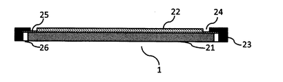
- FIG. 1 is a schematic diagram of a configuration of a liquid crystal display unit 1.
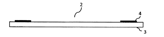
- FIG. 2 is a schematic diagram of a configuration of a protection plate 2.
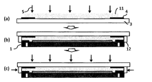
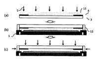
- FIG. It is process drawing which shows 2nd Embodiment of the manufacturing method of this invention. It is process drawing which shows 3rd Embodiment of the manufacturing method of this invention. It is process drawing which shows 4th Embodiment of the manufacturing method of this invention. It is the schematic which shows the one aspect
- the present invention relates to a method of manufacturing an image display device in which a protective plate is bonded to a liquid crystal display unit, wherein the liquid crystal display unit is a liquid crystal display cell, a polarizing plate disposed on the liquid crystal display cell, and the liquid crystal display cell surrounding the polarizing plate.
- the present invention relates to a manufacturing method of an image display device and an image display device including a casing that fixes a liquid crystal display member by surrounding a sealing body or a peripheral wall portion of a liquid crystal display cell.
- An image display device is manufactured by [Step A] to [Step B] and [Step CI] to [Step C-III].
- Step A A step of applying a first curable resin composition, wherein the first curable resin composition having fluidity when uncured is applied to at least one of the liquid crystal display unit or the protective plate.
- Step B A bonding step of bonding the liquid crystal display unit and the protective plate through the first curable resin composition.
- Step CI A first curable resin composition curing step of curing the first curable resin composition and bonding the liquid crystal display unit and the protective plate.
- Step C-II An application step of applying the second curable resin composition to an outer peripheral side surface of the protective plate, the sealing body, or the casing so as to connect the liquid crystal display unit and the protective plate.
- Step C-III A second curable resin composition curing step in which, after the step [C-II], the second curable resin composition is cured to connect the liquid crystal display unit and the protective plate.
- [Step A] and [Step B] are performed in this order, but [Step CI] to [Step C-III] may be performed in any order.
- FIG. 1 is a process diagram showing a first embodiment of a manufacturing process of an image display device (also referred to as “optical member”) of the present invention.
- This method is a method of obtaining an optical member by bonding the liquid crystal display unit 1 and the protective plate 2 together.
- the liquid crystal display unit 1 is a liquid crystal display unit in which a liquid crystal material is sealed between a pair of substrates on which electrodes are formed, and a polarizing plate, a driving circuit, a signal input cable, and a backlight unit are provided.
- FIG. 2 is a cross-sectional view showing a main part of an example of the liquid crystal display unit 1.
- a polarizing plate 22 is disposed on the liquid crystal display cell 21, and a sealing body 23 is disposed on the liquid crystal display cell 21 so as to surround the polarizing plate 22. ing.
- the structure in which the polarizing plate 22 is directly laminated on the liquid crystal display cell 21 is shown, but it is not necessary to directly laminate the polarizing plate 22 as long as the polarizing plate is disposed on the liquid crystal display cell.
- An optical member such as another functional film may be interposed between the cell and the polarizing plate.
- a gap 24 having a maximum width of several mm is formed between the polarizing plate 22 and the sealing body 23, and a sealing film 25 is provided so that the surface of the liquid crystal display cell 21 is not exposed on the bottom surface of the gap 24. Shows an example in which is arranged. That is, as shown in the example of FIG.
- the liquid crystal display which is the bottom surface of the gap 24 between the polarizing plate 22 and the sealing body 23.
- a sealing film 25 having adhesiveness can be disposed to block a part of the gap 24. Since one end of the sealing film 25 in the width direction is adjacent to the polarizing plate 22 and the other end is in close contact with the sealing body 23, the bottom of the gap 24 is sealed.
- the sealing film 25 may not be arranged on the bottom surface of the gap 24 and the surface of the liquid crystal display cell 21 may be exposed.
- an adhesive film having polyethylene terephthalate or the like as a film base and having an adhesive layer such as acrylate or an adhesive layer is preferable.
- the polarizing plate 22 known ones used in image display devices can be used. For example, a film-like absorption polarizer, a wire grid polarizer, or the like can be used.
- the sealing film 25 does not necessarily need to be solid at the time of arrangement
- a backlight side polarizing plate (not shown) can be laminated on the surface opposite to the surface on which the polarizing plate 22 is formed.
- the structure is not limited to the structure in which the backlight side polarizing plate is directly laminated on the liquid crystal display cell 21, and the liquid crystal display cell 21 may be provided with the polarizing plate 22.
- An optical member such as another functional film may be interposed therebetween.
- a backlight (not shown) can be formed on the surface opposite to the surface on which the liquid crystal display cell 21 is disposed.
- the light source constituting the backlight for example, a cold cathode tube, an LED (Light Emitting Diode), or the like can be used.
- an edge light system in which a light source (not shown) is disposed at one end of a light guide plate (not shown) and linear light from the light source is converted into planar light by the light guide plate can be exemplified.
- the backlight method is not limited to the edge light method.
- a direct type system in which a light source is arranged directly below the diffusion plate may be employed.
- the liquid crystal display unit 1 is usually covered with a casing 26.
- the casing 26 is generally made of a metal material. Specifically, an alloy such as stainless steel, iron, aluminum, or silver can be used.
- a liquid crystal display cell, a backlight, a light guide plate, and an optical film can be accommodated in the housing 26.
- a sealing body 23 is disposed so as to cover the liquid crystal display cell 21.
- the sealing body 23 is disposed so as to surround the polarizing film with a gap 24 interposed in the peripheral wall portion of the polarizing film 22.
- the sealing body 23 is coated on the liquid crystal display cell 21 with the sealing film 25 interposed therebetween, but the liquid crystal display cell 21 may be coated directly.
- the sealing body 23 is an example in which the outer wall of the image display device is coated, and in FIG. 2, the casing 26 disposed adjacent to the peripheral wall portion of the liquid crystal display cell 21 is directly coated. In particular, it is not necessary to limit the arrangement.
- the backlight side polarizing plate is laminated on the surface of the liquid crystal display cell 21 opposite to the surface on which the polarizing plate 22 is formed, and the backlight side polarizing plate is further backlit.
- casing 26 can be set as the structure which the sealing body 23 has coat
- an organic polymer material is generally used.
- a protective plate 2 shown in FIG. 3 protects the liquid crystal display unit 1.
- the protective plate 2 is a member having a transparent substrate 3 and a light shielding portion 4 formed on one surface of the transparent substrate 3.
- Examples of the transparent substrate 3 used for the protective plate 2 include a glass plate or a transparent resin plate.
- the transparent substrate 3 has a high transparency with respect to light emitted from the display panel and reflected light, as well as light resistance and low birefringence.
- a glass plate is preferable because it has high plane accuracy, surface scratch resistance, and high mechanical strength.
- the material for the glass plate examples include glass materials such as sodaime glass, and a high transmission glass that is lower than iron and less bluish is more preferable. In order to improve safety, tempered glass may be used as a surface material. In particular, when a thin glass plate is used, it is preferable to use a chemically strengthened glass plate.
- the material for the transparent resin plate include highly transparent resin materials such as a polymethyl methacrylate (PMMA) plate, a polycarbonate (PC) plate, and an alicyclic polyolefin polymer (COP) plate.
- PMMA polymethyl methacrylate
- PC polycarbonate
- COP alicyclic polyolefin polymer
- the protective plate 2 may be subjected to a surface treatment in order to improve the interfacial adhesive force with the cured resin layer.
- a surface treatment method include a method of treating the surface of the protective plate 2 with a silane coupling agent, a method of forming a silicon oxide thin film by an oxidation flame using a frame burner, and the like.
- the protective plate 2 is obtained by curing the first cured layer 13 or the second curable resin composition obtained by curing the first curable resin composition described later in order to increase the contrast of the display image.
- An antireflection layer may be provided on the surface opposite to the side on which the second cured product layer 14 is formed.
- the antireflection layer can be provided by a method of directly forming an inorganic thin film on the surface of the protective plate 2 or a method of bonding a transparent resin film provided with an antireflection layer to the protective plate 2.
- a part or the whole of the protective plate 2 is colored, or a part or the whole of the surface of the protective plate 2 is polished to form a glass to scatter light, or a part of the surface of the protective plate 2 is scattered.
- the transmitted light may be refracted or reflected by forming fine irregularities on the entire surface.
- a colored film, a light scattering film, a photorefractive film, a light reflecting film or the like may be attached to a part or the whole of the surface of the protective plate 2.
- the shape of the protection plate 2 is usually rectangular.
- the size of the protective plate 2 is suitably 0.5 m ⁇ 0.4 m in the case of a television receiver because the manufacturing method of the present invention is particularly suitable for manufacturing a relatively large area image display device. 0.7 m ⁇ 0.4 m or more is particularly preferable.
- the upper limit of the size of the protection plate 2 is often determined by the size of the display panel. Also, an image display device that is too large is likely to be difficult to handle during installation or the like.
- the upper limit of the size of the protective plate 2 is usually about 2.5 m ⁇ 1.5 m due to these restrictions.
- the thickness of the protective plate 2 is usually 0.5 to 25 mm in the case of a glass plate in view of mechanical strength, transparency and the like. For applications such as television receivers and PC displays used indoors, 1 to 6 mm is preferable from the viewpoint of reducing the weight of the display device, and for public display applications installed outdoors, 3 to 20 mm is preferable. When chemically strengthened glass is used, the thickness of the glass is preferably about 0.5 to 1.5 mm in terms of strength. In the case of a transparent resin plate, 2 to 10 mm is preferable.
- the light-shielding portion 4 hides the wiring member connected to the display panel so that the area other than the image display area of the liquid crystal display cell to be described later cannot be seen from the protective plate 2 side.
- the light shielding unit 4 can be formed on the surface on the side where the second cured product layer 14 to the first cured product layer 13 described later are formed, and reduces the parallax between the light shielding unit 4 and the image display area.
- the protective plate 2 is a glass plate, it is preferable to use ceramic printing containing a black pigment in the light-shielding printing portion because of high light shielding properties.
- the light shielding part 4 may be provided on the surface to be bonded to the protective plate 2, and a film provided with an antireflection layer on the back surface thereof, that is, the outermost surface of the display device may be bonded to the protective plate.
- the light-shielding portion 4 is formed by attaching a tape, applying paint, printing, or the like.
- the present invention can also be applied to a device that does not have the light shielding portion 4.
- the case where the light shielding portion 4 is provided will be described as a specific example.
- the protective plate 2 which has the light-shielding part 4 for the 1st curable resin composition 11 containing the (meth) acrylate (A) mentioned later and a photoinitiator (B). It is applied to the surface of the surface on which the light shielding portion 4 is formed.
- the coating method include a slit coater, a roll coater, a spin coater, and a screen printing method.
- coats the 1st curable resin composition on the protective plate 2 was illustrated, you may apply
- the 1st curable resin composition 11 should just be apply
- the storage rigidity at 25 ° C. of the first cured product layer obtained by curing the first curable resin composition 11 is preferably 10 2 to 10 7 Pa, preferably 10 2 to 10 5 Pa is more preferable. Furthermore, 10 2 to 10 4 Pa is particularly preferable in order to eliminate the void at the time of bonding in a shorter time. If the storage rigidity is 10 3 Pa or more, the shape of the first cured product layer 13 is easily maintained. Moreover, even when the thickness of the first curable resin composition 11 to be formed is relatively thick, the thickness can be kept uniform throughout the first cured product layer 13, and the protective plate 2 and the liquid crystal display unit 1 can be maintained.
- the storage rigidity is 10 7 Pa or less, good adhesion can be exhibited.
- the molecular mobility of the resin material to be formed is relatively high, the liquid crystal display unit 1 and the protective plate 2 are bonded together in a reduced pressure atmosphere, and then returned to the atmospheric pressure atmosphere.
- the void volume tends to decrease due to the differential pressure between the pressure of the material (with reduced pressure) and the pressure applied to the hardened material layer of the fill material (atmospheric pressure). Easily dissolved and absorbed.
- the thickness of the first curable resin composition 11 is preferably 50 to 500 ⁇ m, more preferably 50 to 350 ⁇ m, and particularly preferably 100 to 350 ⁇ m. If the thickness of the 1st curable resin composition 11 is 50 micrometers or more, the 1st hardened
- cured material layer 13 is 500 micrometers or less, a space
- the liquid first curable resin composition supplied to the surface of the protective plate 2 while adjusting the thickness of the second cured product layer 14 described later. 11 is a method for adjusting the supply amount.
- the viscosity of the first curable resin composition 11 is preferably 0.05 to 50 Pa ⁇ s, and more preferably 1 to 20 Pa ⁇ s. If the viscosity is 0.05 Pa ⁇ s or more, a decrease in physical properties of the first cured product layer 13 is suppressed. Moreover, since the component having a low boiling point is reduced, volatilization in a reduced-pressure atmosphere described later is suppressed, which is preferable. If the viscosity is 50 Pa ⁇ s or less, voids hardly remain in the first cured product layer 13. The viscosity of the first curable resin composition 11 is measured using an E-type viscometer at 25 ° C.
- the first curable resin composition 11 may be a photocurable resin composition or a thermosetting resin composition.
- a photocurable resin composition containing a curable compound and a photopolymerization initiator is preferable because it can be cured at a low temperature and has a high curing rate.
- the first curable resin composition 11 may be used for pasting without being cured, but is preferably temporarily cured as described in FIG. Specifically, the coating film of the first curable resin composition 11 after application is irradiated with ultraviolet rays 5, and a cured portion (on the transparent substrate side as viewed from the curable resin composition) on the lower side of the application layer (on the transparent substrate side) A cured product layer having an uncured portion (not shown in the figure) existing on the upper side (opposite side of the transparent substrate side) of the coating layer (on the atmosphere side when performed in the atmosphere) is obtained.
- the irradiation amount is preferably 5 to 2000 mJ / cm 2 , more preferably 10 to 1000 mJ / cm 2 , and particularly preferably 10 to 500 mJ / cm 2 . If the amount of irradiation is too small, the degree of cure of the resin of the optical member finally bonded may be insufficient. If the amount of irradiation is too large, the amount of uncured components decreases, and the liquid crystal display unit 1 and the light-shielding portion are removed. Bonding of the protective plate 2 may be poor.
- “uncured” refers to a fluid state in a 25 ° C. environment.
- any light source may be used as long as it is a lamp that irradiates ultraviolet to near ultraviolet rays.
- a low-pressure, high-pressure or ultrahigh-pressure mercury lamp, metal halide lamp, (pulse) xenon lamp, LED lamp or electrodeless lamp can be used.
- step 1 of the present invention when the maximum illuminance in the range of 320 nm to 450 nm is 100, the ratio of the maximum illuminance at 200 to 320 nm (illuminance ratio) ) Is 30 or less, and particularly preferably, the illuminance at 200 to 320 nm is 10 or less.
- the maximum illuminance in the range of 320 nm to 450 nm is 100, if the ratio of maximum illuminance (illuminance ratio) at 200 to 320 nm is higher than 30, the adhesive strength of the finally obtained optical member will be inferior.
- the illuminance is usually 30 to 1000 mW / cm 2 at each wavelength (for example, 365 nm).
- the method of irradiating ultraviolet rays so as to achieve the above illuminance ratio includes, for example, a method of applying a lamp that satisfies the illuminance ratio as a lamp that irradiates ultraviolet to near ultraviolet rays, Even if the above condition is not satisfied, such illuminance can be obtained by using a base material (for example, a short wave ultraviolet cut filter, a glass plate, a film, etc.) that cuts short wavelength ultraviolet rays at the time of irradiation in step 1. Irradiation at a ratio is possible. Although it does not specifically limit as a base material which adjusts the illumination intensity ratio of an ultraviolet-ray, For example, the glass plate, soda-lime glass, PET film etc.
- the ultraviolet rays from the upper surface (on the side opposite to the transparent substrate as viewed from the curable resin composition layer) (normal air surface) on the coating side in normal air. Further, ultraviolet irradiation may be performed while spraying a curing-inhibiting gas on the upper surface of the coating layer after evacuation.
- the side opposite to the liquid crystal display unit side or the side opposite to the transparent substrate side is the atmosphere side.
- the state of the uncured portion and the film thickness of the uncured portion can be adjusted by spraying oxygen or ozone onto the surface of the ultraviolet curable resin layer (coating layer) during the ultraviolet irradiation. That is, by spraying oxygen or ozone on the surface of the coating layer, oxygen inhibition of curing of the curable resin composition occurs on the surface, so that the uncured portion of the surface can be ensured, The film thickness can be increased.
- the curing rate represents the curing rate as seen from the curing component of the curable resin composition, and represents a value calculated by excluding components that are not cured such as a softening agent.
- the curing shrinkage can be calculated from the following formula (1) from the liquid specific gravity before curing at 25 ° C. and the film specific gravity at 25 ° C. obtained by curing.
- the first curable resin composition 11 used in the present invention has the above-mentioned [Step CI] or [Step C] with respect to the storage rigidity at 25 ° C. of the resin layer when irradiated with ultraviolet rays in the above [Step B].
- the storage rigidity of the resin layer when irradiated with ultraviolet rays is preferably 3 to 20 times (preferably 3 to 10 times).
- it can be measured by the following method. Specifically, two 40 ⁇ m-thick PET films coated with a fluorine-based mold release agent are prepared, and a film obtained by curing the obtained curable resin composition on one of the release agent-coated surfaces.
- the two PET films are bonded together so that the respective release agent application surfaces face each other.
- the resin composition is cured by irradiating ultraviolet rays with an integrated light quantity of 2000 mJ / cm 2 with a high-pressure mercury lamp (80 W / cm, ozone-less) through a PET film.
- the two PET films are peeled off to produce a cured product for measuring the rigidity.
- the rigidity can be measured in a temperature range of 20 to 40 ° C. using ARES (TA Instruments).
- the curing rate during the main curing in [Step CI] is 95% or more.
- the first curable resin composition 11 used in the present invention preferably has a storage rigidity of 1 ⁇ 10 2 Pa to 1 ⁇ 10 4 Pa at 25 ° C. during the temporary curing. If the storage rigidity is greater than 1 ⁇ 10 4 Pa, the first curable resin composition 11 has a shrinking force due to curing, so the first curable resin composition 11 does not follow the substrate, When peeling occurs, the substrate is distorted, or the stress is not sufficiently relaxed, display unevenness occurs when an optical member is obtained.
- the storage rigidity at the time of pre-curing is in the above range, so that the space created at the time of bonding can be made of resin without causing problems when moved to atmospheric pressure. It becomes possible to fill.
- the storage rigidity is preferably 300 to 3000 Pa, and more preferably 500 to 2000 Pa.
- the curing rate of the resin at the time of temporary curing is 60 to 90%, and the storage rigidity of the cured product having the curing rate is the above value and the preferable value, thereby preventing the distortion and display unevenness of the substrate. it can.
- the curing rate at the time of main curing in [Step CI] described later is usually 95% or more.
- the storage rigidity of the resin layer when irradiated with ultraviolet rays in [Step CI] described later is 1. It is preferable to use a resin composition of 5 to 10 times.
- the storage rigidity of the resin layer when irradiated with ultraviolet rays at a curing rate of 98% is 1.5% with respect to the storage rigidity at 25 ° C. of the resin layer when irradiated with ultraviolet rays at a curing rate of 80%. It is preferable to use a resin composition of up to 10 times.
- the storage rigidity of the resin layer when irradiated with ultraviolet rays in [Step CI] or [Step C-III] described later is 2 It is more preferably 7 times, and particularly preferably 2.5 to 5 times.
- the storage rigidity of the resin layer when irradiated with ultraviolet rays at a curing rate of 98% is 2 to 7 with respect to the storage rigidity at 25 ° C. of the resin layer when irradiated with ultraviolet rays at a curing rate of 80%. Is preferably doubled, and is particularly preferably 2.5 to 5 times.
- the curable resin composition used in the method of the present invention has a storage rigidity at 25 ° C. of 1 ⁇ 10 3 Pa to 1 ⁇ 10 6 Pa is preferable.
- the storage rigidity is higher than 1 ⁇ 10 6 Pa, the shrinkage of the curable resin composition becomes too large due to curing, and thus the base material may be distorted or the stress is not sufficiently relaxed. The possibility of display unevenness when the member is obtained is reduced.
- the storage rigidity is preferably 1.0 ⁇ 10 3 to 1.0 ⁇ 10 5 Pa, and more preferably 1.0 ⁇ 10 3 to 3.0 ⁇ 10 4 Pa.
- Step B Next, with the liquid crystal display unit 1 and the surface of the protective plate 2 on which the first curable resin composition 11 is formed facing each other, as shown in FIG.
- the protective plate 2 which has is bonded together. Bonding can be performed either in air or in vacuum. Here, in order to make it easy to prevent bubbles from being generated at the time of bonding, it is preferable to bond in a vacuum.
- the first curable resin composition 11 is bonded together after obtaining a cured product of an ultraviolet curable resin having a cured portion and an uncured portion, an improvement in adhesion can be expected.
- the 1st curable resin composition 11 is spread by press etc., and the 1st curable resin composition 11 is filled in space.
- the first cured product layer 13 with few or no voids is formed when exposed to a high pressure atmosphere thereafter.
- a reduced pressure atmosphere it is 1 kPa or less, preferably 10 to 300 Pa, more preferably 15 to 100 Pa. You may cancel
- the first curable resin composition 11 flows in the space, and the interval between the liquid crystal display unit 1 and the protective plate 2 is made uniform. It becomes easier to do.
- the optical member obtained by bonding the protective plate 2 and the liquid crystal display unit 1 is irradiated with the ultraviolet rays 5 from the protective plate 2 side, and a curable resin composition (coating) Layer).
- the dose of ultraviolet rays is preferably from about 100 ⁇ 4000mJ / cm 2 in accumulated light quantity, particularly preferably from 200 ⁇ 3000mJ / cm 2 or so, more highly preferably 1500 ⁇ 3000mJ / cm 2.
- the light source used for curing by irradiation with ultraviolet to near ultraviolet light may be any lamp as long as it is a lamp that emits ultraviolet to near ultraviolet light.
- a low-pressure, high-pressure or ultrahigh-pressure mercury lamp, metal halide lamp, (pulse) xenon lamp, LED lamp, or electrodeless lamp may be used.
- Step C-II Furthermore, as shown in FIG.1 (c), the liquid crystal display unit 1 and a protective plate are connected with the 2nd curable resin composition 12 containing the (meth) acrylate (A) and photoinitiator (B) which are mentioned later.
- the 2nd curable resin composition 12 containing the (meth) acrylate (A) and photoinitiator (B) which are mentioned later.
- coat coat to the outer peripheral side part of the sealing body 23 on the protective plate 2.
- the second curable resin composition 12 may be applied to the outer peripheral side surface of the sealing body 23 or the housing 26, As a result, the liquid crystal display unit 1 and the protective plate need only be connected.
- coats the 2nd curable resin composition 12 on the protective plate 2 was illustrated, another optical member may intervene between the protective plate 2 and the 2nd curable resin composition 12.
- the outer peripheral side surface portion of the housing 26 is applied as the second curable resin composition to the outer peripheral side surface portion of the housing 26.
- the form of the liquid crystal display unit 1 or the form of application is particularly applicable if the second curable resin composition is applied to the outer peripheral side surface of the housing 26.
- the form is not limited.
- Examples of the application method include a dispensing method.
- the first curable resin composition and the second curable resin composition applied to the surfaces of the liquid crystal display unit 1 and the protective plate 2 may be the same or different curable resin compositions may be used. I do not care.
- the 2nd curable resin composition 12 is apply
- the second curable resin composition 12 is applied to the outer peripheral side surface portion of the casing 26 that fixes the sealing body 23 or the liquid crystal display unit 1 while avoiding the projection area of the liquid crystal display cell, so that the second curable resin composition is applied.
- curing the resin composition 12 is formed in the outer peripheral side part of the housing
- the pressure does not easily propagate to the liquid crystal display cell. It can be prevented from occurring.
- the second cured product layer 12 is laminated on the display region of the liquid crystal display cell or the polarizing plate, ripples are generated due to interference when pressure is applied to the second cured product layer or the peripheral wall portion of the image display region. It will be.
- the second cured product layer 14 is laminated in this manner, the distance between the protective plate 2 and the liquid crystal display unit 1 can be maintained, and even when pressed by a finger or the like, the pressure is transmitted to the liquid crystal display unit or the polarizing plate.
- the application of the second curable resin composition 12 is preferably formed in a rectangular frame shape along the outer peripheral side surface of the casing 26 that fixes the sealing body 23 or the liquid crystal display unit 1. Moreover, you may apply
- the coating thickness of the second curable resin composition 12 may be sufficient to connect the liquid crystal display unit and the protective plate, but is thicker than the thickness of the first curable resin composition 11 to be formed. Become.
- the thickness of the first curable resin composition 11 to be formed is preferably 0.01 to 10 mm thick, more preferably 0.1 to 5 mm thick, and more preferably 0.5 to 3 mm thick.
- the storage rigidity at 25 ° C. at the time of curing in the second curable resin composition 12 is preferably larger than the storage rigidity at 25 ° C. of the cured product layer of the first curable resin composition 11.
- the liquid crystal display unit 1 and the protective plate 2 are When connecting, since it is strong against deformation due to external pressure and can be connected more firmly, the influence on the gap thickness of the first curable resin layer can be reduced.
- the second curable resin composition 12 and the first curable resin so that the shrinkage rate at the time of curing of the second curable resin composition 12 is larger than the shrinkage rate at the time of curing of the first curable resin composition 11. It is preferable to design the composition 11. In the first cured product layer 13 formed by curing the first curable resin composition 11, it is considered that the shrinkage stress corresponding to the shrinkage rate at the time of curing remains in the thickness direction of the first cured product layer 13. In addition, the thickness of the first cured product layer 13 slightly decreases due to the shrinkage stress in the thickness direction remaining in the layered portion at the time of curing. By using the first curable resin composition 11 having a smaller shrinkage rate at the time of curing than the second curable resin composition 12, it is possible to relieve the stress in the display region and suppress the occurrence of display unevenness.
- One of means for increasing the shrinkage rate at the time of curing of the second curable resin composition 12 to be larger than the shrinkage rate at the time of curing of the first curable resin composition 11 is that of the curable group of the second curable resin composition 12.
- the number is to be larger than the number of curable groups of the first curable resin composition 11.
- the viscosity of the second curable resin composition 12 may be higher than the viscosity of the first curable resin composition 11.
- the uncured viscosity of the second curable resin composition 12 is preferably 2 times or more, more preferably 5 times or more of the uncured viscosity of the first curable resin composition 11. More than double is more preferable.
- the viscosity at the time of uncured at 25 degreeC of the 2nd curable resin composition 12 shall be 3000 Pa.s or less. Is preferred.
- the preferable viscosity of the second curable resin composition 12 is specifically 40 to 70 Pa ⁇ s. If it is less than 40 Pa ⁇ s, the second curable resin composition 12 cannot maintain its shape and spreads, and it becomes difficult to control the thickness. The thing 12 may be destroyed. On the other hand, when the viscosity exceeds 70 Pa ⁇ s, it may be difficult to discharge from the applicator.
- the second curable resin composition 12 may be a photocurable resin composition or a thermosetting resin composition.
- the photocurable resin composition containing a curable compound and a photoinitiator is preferable from the point which can be hardened
- uncured refers to a fluid state in a 25 ° C. environment.
- any light source may be used as long as it is a lamp that irradiates ultraviolet to near ultraviolet rays.
- a low-pressure, high-pressure or ultrahigh-pressure mercury lamp, metal halide lamp, (pulse) xenon lamp, LED lamp or electrodeless lamp can be used.
- the thickness of the coating film 11 of the first curable resin composition and the thickness of the coating film of the second curable resin composition 12 were measured using a laser displacement meter (LK-H052K, manufactured by Keyence Corporation) It can be obtained by measuring the total thickness of the coating film of the first curable resin composition 11 or the coating film of the second curable resin composition 12 formed thereon. Also, depending on the surface shape of the coating film of the first curable resin composition 11 or the coating film of the second curable resin composition 12, it may be difficult to measure the thickness with the laser displacement meter.
- the thickness of the coating film of the first curable resin composition 11 and the thickness of the coating film of the second curable resin composition 12 are measured using a 3D shape measuring machine (high precision shape measuring system KS-1100) or the like. You may measure.
- the 2nd curable resin composition 12 is hardened and the 2nd hardened
- the curing means includes heat or light, but it is preferable to cure by irradiating light. Although it does not specifically limit as a direction of light irradiation, It is preferable to irradiate from the side part of the image display apparatus obtained, or to irradiate from the liquid crystal display unit 1 side.
- the dose of ultraviolet rays is preferably from about 100 ⁇ 4000mJ / cm 2 in accumulated light quantity, particularly preferably from 200 ⁇ 3000mJ / cm 2 or so, more highly preferably 1500 ⁇ 3000mJ / cm 2.
- the light source used for curing by irradiation with ultraviolet to near ultraviolet light may be any lamp as long as it is a lamp that emits ultraviolet to near ultraviolet light.
- a low-pressure, high-pressure or ultrahigh-pressure mercury lamp, metal halide lamp, (pulse) xenon lamp, LED lamp, or electrodeless lamp may be used. In this way, the image display device shown in FIG. 7 can be obtained.
- FIG. 4 is a process diagram showing a second embodiment of the optical member manufacturing process of the present invention.
- This method is a method of obtaining an optical member (image display device) by bonding the liquid crystal display unit 1 and the protective plate 2 together. Note that portions other than the parts changed from the first embodiment can be taken in by reflecting the matters described in the first embodiment, and descriptions that partially overlap are omitted.
- the 1st curable resin composition 11 containing the (meth) acrylate (A) and photoinitiator (B) mentioned later of the protection plate 2 which has the light-shielding part 4 is shown. It is applied to the surface of the surface where the light shielding part 4 is formed.
- the coating method include a slit coater, a roll coater, a spin coater, and a screen printing method.
- coats the 1st curable resin composition on the protective plate 2 was illustrated, you may apply
- the 1st curable resin composition 11 should just be apply
- the first curable resin composition 11 may be a photocurable resin composition or a thermosetting resin composition.
- a photocurable resin composition containing a curable compound and a photopolymerization initiator is preferable because it can be cured at a low temperature and has a high curing rate.
- the first curable resin composition 11 may be used for pasting without being cured, but is preferably temporarily cured as described in FIG. Specifically, the coating film of the first curable resin composition 11 after application is irradiated with ultraviolet rays 5, and a cured portion (on the transparent substrate side as viewed from the curable resin composition) on the lower side of the application layer (on the transparent substrate side) A cured product layer having an uncured portion (not shown in the figure) existing on the upper side (opposite side of the transparent substrate side) of the coating layer (on the atmosphere side when performed in the atmosphere) is obtained.
- the irradiation amount is preferably 5 to 2000 mJ / cm 2 , more preferably 10 to 1000 mJ / cm 2 , and particularly preferably 10 to 500 mJ / cm 2 . If the amount of irradiation is too small, there is a risk that the degree of cure of the resin of the optical member that is finally bonded will be insufficient. There is a possibility that the bonding of the protective plate 2 will be poor.
- “uncured” refers to a fluid state in a 25 ° C. environment. In addition, when the resin composition layer is touched with a finger after ultraviolet irradiation and a liquid component adheres to the finger, it is determined to have an uncured portion.
- Step B Next, with the liquid crystal display unit 1 and the surface of the protective plate 2 on which the first curable resin composition 11 is formed facing each other, as shown in FIG.
- the protective plate 2 which has is bonded together. Bonding can be performed either in air or in vacuum. Here, in order to make it easy to prevent bubbles from being generated at the time of bonding, it is preferable to bond in a vacuum.
- the first curable resin composition 11 is bonded together after obtaining a cured product of an ultraviolet curable resin having a cured portion and an uncured portion, an improvement in adhesion can be expected.
- the 1st curable resin composition 11 is spread by press etc., and the 1st curable resin composition 11 is filled in space.
- the first cured product layer 13 with few or no voids is formed when exposed to a high pressure atmosphere thereafter.
- a reduced pressure atmosphere it is 1 kPa or less, preferably 10 to 300 Pa, more preferably 15 to 100 Pa. You may cancel
- the first curable resin composition 11 flows in the space, and the interval between the liquid crystal display unit 1 and the protective plate 2 is made uniform. It becomes easier to do.
- Step C-II Furthermore, as shown in FIG. 4B, the liquid crystal display unit 1 and the protective plate are connected to the second curable resin composition 12 containing the (meth) acrylate (A) and the photopolymerization initiator (B) described above.
- the second curable resin composition 12 may be applied to the outer peripheral side surface of the sealing body 23 or the housing 26, As a result, the liquid crystal display unit 1 and the protective plate need only be connected.
- coats the 2nd curable resin composition 12 on the protective plate 2 was illustrated, another optical member may intervene between the protective plate 2 and the 2nd curable resin composition 12.
- the outer peripheral side surface portion of the housing 26 is applied as the second curable resin composition to the outer peripheral side surface portion of the housing 26.
- the form of the liquid crystal display unit 1 or the form of application is particularly applicable if the second curable resin composition is applied to the outer peripheral side surface of the housing 26.
- the form is not limited.
- Examples of the application method include a dispensing method.
- the first curable resin composition and the second curable resin composition applied to the surfaces of the liquid crystal display unit 1 and the protective plate 2 may be the same or different curable resin compositions may be used. I do not care.
- the application of the second curable resin composition 12 is preferably formed in a rectangular frame shape along the outer peripheral side surface of the casing 26 that fixes the sealing body 23 or the liquid crystal display unit 1. Moreover, you may apply
- the coating thickness of the second curable resin composition 12 may be sufficient to connect the liquid crystal display unit and the protective plate, but is thicker than the thickness of the first curable resin composition 11 to be formed. Become.
- the thickness of the first curable resin composition 11 to be formed is preferably 0.01 to 10 mm thick, more preferably 0.1 to 5 mm thick, and more preferably 0.5 to 3 mm thick.
- the storage rigidity at 25 ° C. at the time of curing in the second curable resin composition 12 is preferably larger than the storage rigidity at 25 ° C. of the cured product layer of the first curable resin composition 11.
- the liquid crystal display unit 1 and the protective plate 2 are When connecting, since it is strong against deformation due to external pressure and can be connected more firmly, the influence on the gap thickness of the first curable resin layer can be reduced.
- the second curable resin composition 12 may be a photocurable resin composition or a thermosetting resin composition.
- the photocurable resin composition containing a curable compound and a photoinitiator is preferable from the point which can be hardened
- the optical member obtained by bonding the protective plate 2 and the liquid crystal display unit 1 is irradiated with the ultraviolet-ray 5 from the protective plate 2 side, and curable resin composition (application
- the second curable resin composition 12 is cured to form the second cured product layer 14.
- the dose of ultraviolet rays is preferably from about 100 ⁇ 4000mJ / cm 2 in accumulated light quantity, particularly preferably from 200 ⁇ 3000mJ / cm 2 or so, more highly preferably 1500 ⁇ 3000mJ / cm 2.
- the light source used for curing by irradiation with ultraviolet to near ultraviolet light may be any lamp as long as it is a lamp that emits ultraviolet to near ultraviolet light.
- a low-pressure, high-pressure or ultrahigh-pressure mercury lamp, metal halide lamp, (pulse) xenon lamp, LED lamp, or electrodeless lamp may be used. In this way, the image display device shown in FIG. 7 can be obtained.
- FIG. 5 is a process diagram showing a third embodiment of the manufacturing process of the optical member of the present invention.
- This method is a method of obtaining an optical member (image display device) by bonding the liquid crystal display unit 1 and the protective plate 2 together. Note that portions other than the parts changed from the first embodiment can be taken in by reflecting the matters described in the first embodiment, and descriptions that partially overlap are omitted.
- the 1st curable resin composition 11 containing the (meth) acrylate (A) and photoinitiator (B) mentioned later of the protection plate 2 which has the light-shielding part 4 is shown. It is applied to the surface of the surface where the light shielding part 4 is formed.
- the coating method include a slit coater, a roll coater, a spin coater, and a screen printing method.
- coats the 1st curable resin composition on the protective plate 2 was illustrated, you may apply
- the 1st curable resin composition 11 should just be apply
- the first curable resin composition 11 may be a photocurable resin composition or a thermosetting resin composition.
- a photocurable resin composition containing a curable compound and a photopolymerization initiator is preferable because it can be cured at a low temperature and has a high curing rate.
- the first curable resin composition 11 may be used for pasting without curing, but is preferably temporarily cured as described in FIG. Specifically, the coating film of the first curable resin composition 11 after application is irradiated with ultraviolet rays 5, and a cured portion (on the transparent substrate side as viewed from the curable resin composition) on the lower side of the application layer (on the transparent substrate side) A cured product layer having an uncured portion (not shown in the figure) existing on the upper side (opposite side of the transparent substrate side) of the coating layer (on the atmosphere side when performed in the atmosphere) is obtained.
- the irradiation amount is preferably 5 to 2000 mJ / cm 2 , more preferably 10 to 1000 mJ / cm 2 , and particularly preferably 10 to 500 mJ / cm 2 . If the amount of irradiation is too small, there is a risk that the degree of cure of the resin of the optical member that is finally bonded will be insufficient. There is a possibility that the bonding of the protective plate 2 will be poor.
- “uncured” refers to a fluid state in a 25 ° C. environment. In addition, when the resin composition layer is touched with a finger after ultraviolet irradiation and a liquid component adheres to the finger, it is determined to have an uncured portion.
- Step B Next, with the liquid crystal display unit 1 and the surface of the protective plate 2 on which the first curable resin composition 11 is formed facing each other, as shown in FIG.
- the protective plate 2 which has is bonded together. Bonding can be performed either in air or in vacuum. Here, in order to make it easy to prevent bubbles from being generated at the time of bonding, it is preferable to bond in a vacuum.
- the first curable resin composition 11 is bonded together after obtaining a cured product of an ultraviolet curable resin having a cured portion and an uncured portion, an improvement in adhesion can be expected.
- the 1st curable resin composition 11 is spread by press etc., and the 1st curable resin composition 11 is filled in space.
- the first cured product layer 13 with few or no voids is formed when exposed to a high pressure atmosphere thereafter.
- a reduced pressure atmosphere it is 1 kPa or less, preferably 10 to 300 Pa, more preferably 15 to 100 Pa. You may cancel
- the first curable resin composition 11 flows in the space, and the interval between the liquid crystal display unit 1 and the protective plate 2 is made uniform. It becomes easier to do.
- Step C-II Furthermore, as shown in FIG. 5B, the liquid crystal display unit 1 and the protective plate are connected to the second curable resin composition 12 containing the (meth) acrylate (A) and the photopolymerization initiator (B) described above.
- the second curable resin composition 12 may be applied to the outer peripheral side surface of the sealing body 23 or the housing 26, As a result, the liquid crystal display unit 1 and the protective plate need only be connected.
- coats the 2nd curable resin composition 12 on the protective plate 2 was illustrated, another optical member may intervene between the protective plate 2 and the 2nd curable resin composition 12.
- the outer peripheral side surface portion of the housing 26 is applied as the second curable resin composition to the outer peripheral side surface portion of the housing 26.
- the form of the liquid crystal display unit 1 or the form of application is particularly applicable if the second curable resin composition is applied to the outer peripheral side surface of the housing 26.
- the form is not limited.
- Examples of the application method include a dispensing method.
- the first curable resin composition and the second curable resin composition applied to the surfaces of the liquid crystal display unit 1 and the protective plate 2 may be the same or different curable resin compositions may be used. I do not care.
- coating to the 2nd curable resin composition 12 is formed in the rectangular frame shape so that the outer peripheral side part of the housing
- the coating thickness of the second curable resin composition 12 may be sufficient to connect the liquid crystal display unit and the protective plate, but is thicker than the thickness of the first curable resin composition 11 to be formed. Become.
- the thickness of the first curable resin composition 11 to be formed is preferably 0.01 to 10 mm thick, more preferably 0.1 to 5 mm thick, and more preferably 0.5 to 3 mm thick.
- the storage rigidity at 25 ° C. at the time of curing in the second curable resin composition 12 is preferably larger than the storage rigidity at 25 ° C. of the cured product layer of the first curable resin composition 11.
- the liquid crystal display unit 1 and the protective plate 2 are When connecting, since it is strong against deformation due to external pressure and can be connected more firmly, the influence on the gap thickness of the first curable resin layer can be reduced.
- the second curable resin composition 12 may be a photocurable resin composition or a thermosetting resin composition.
- the photocurable resin composition containing a curable compound and a photoinitiator is preferable from the point which can be hardened
- the 2nd curable resin composition 12 is hardened
- the curing means includes heat or light, but it is preferable to cure by irradiating light. Although it does not specifically limit as a direction of light irradiation, It is preferable to irradiate from the side part of the image display apparatus obtained, or to irradiate from the liquid crystal display unit 1 side.
- the dose of ultraviolet rays is preferably from about 100 ⁇ 4000mJ / cm 2 in accumulated light quantity, particularly preferably from 200 ⁇ 3000mJ / cm 2 or so, more highly preferably 1500 ⁇ 3000mJ / cm 2.
- the light source used for curing by irradiation with ultraviolet to near ultraviolet light may be any lamp as long as it is a lamp that emits ultraviolet to near ultraviolet light.
- a low-pressure, high-pressure or ultrahigh-pressure mercury lamp, metal halide lamp, (pulse) xenon lamp, LED lamp, or electrodeless lamp may be used.
- the optical member obtained by bonding the protective plate 2 and the liquid crystal display unit 1 is irradiated with the ultraviolet rays 5 from the protective plate 2 side, and a curable resin composition (coating) Layer).
- the dose of ultraviolet rays is preferably from about 100 ⁇ 4000mJ / cm 2 in accumulated light quantity, particularly preferably from 200 ⁇ 3000mJ / cm 2 or so, more highly preferably 1500 ⁇ 3000mJ / cm 2.
- the light source used for curing by irradiation with ultraviolet to near ultraviolet light may be any lamp as long as it is a lamp that emits ultraviolet to near ultraviolet light.
- a low-pressure, high-pressure or ultrahigh-pressure mercury lamp, metal halide lamp, (pulse) xenon lamp, LED lamp, or electrodeless lamp may be used.
- the image display device shown in FIG. 7 can be obtained.
- FIG. 6 is a process diagram showing a fourth embodiment of a process for producing an optical member of the present invention.
- This method is a method of obtaining an optical member (image display device) by bonding the liquid crystal display unit 1 and the protective plate 2 together. Note that portions other than the parts changed from the first embodiment can be taken in by reflecting the matters described in the first embodiment, and descriptions that partially overlap are omitted.
- the 1st curable resin composition 11 containing the (meth) acrylate (A) and photoinitiator (B) mentioned later of the protection plate 2 which has the light-shielding part 4 is used. It is applied to the surface of the surface where the light shielding part 4 is formed.
- the coating method include a slit coater, a roll coater, a spin coater, and a screen printing method.
- coats the 1st curable resin composition on the protective plate 2 was illustrated, you may apply
- the 1st curable resin composition 11 should just be apply
- the first curable resin composition 11 may be a photocurable resin composition or a thermosetting resin composition.
- a photocurable resin composition containing a curable compound and a photopolymerization initiator is preferable because it can be cured at a low temperature and has a high curing rate.
- the first curable resin composition 11 may be used for pasting without curing, but is preferably temporarily cured as described in FIG. Specifically, the coating film of the first curable resin composition 11 after application is irradiated with ultraviolet rays 5, and a cured portion (on the transparent substrate side as viewed from the curable resin composition) on the lower side of the application layer (on the transparent substrate side) A cured product layer having an uncured portion (not shown in the figure) existing on the upper side (opposite side of the transparent substrate side) of the coating layer (on the atmosphere side when performed in the atmosphere) is obtained.
- the irradiation amount is preferably 5 to 2000 mJ / cm 2 , more preferably 10 to 1000 mJ / cm 2 , and particularly preferably 10 to 500 mJ / cm 2 . If the amount of irradiation is too small, there is a risk that the degree of cure of the resin of the optical member that is finally bonded will be insufficient. There is a possibility that the bonding of the protective plate 2 will be poor.
- “uncured” refers to a fluid state in a 25 ° C. environment. In addition, when the resin composition layer is touched with a finger after ultraviolet irradiation and a liquid component adheres to the finger, it is determined to have an uncured portion.
- Step B Next, as shown in FIG. 6B, the liquid crystal display unit 1 and the light shielding portion are arranged so that the liquid crystal display unit 1 and the surface of the protective plate 2 coated with the first curable resin composition 11 face each other.
- the protective plate 2 which has is bonded together. Bonding can be performed either in air or in vacuum. Here, in order to make it easy to prevent bubbles from being generated at the time of bonding, it is preferable to bond in a vacuum.
- the first curable resin composition 11 is bonded together after obtaining a cured product of an ultraviolet curable resin having a cured portion and an uncured portion, an improvement in adhesion can be expected.
- the 1st curable resin composition 11 is spread by press etc., and the 1st curable resin composition 11 is filled in space.
- the first cured product layer 13 with few or no voids is formed when exposed to a high pressure atmosphere thereafter.
- pasting is performed in a reduced pressure atmosphere, it is 1 kPa or less, preferably 10 to 300 Pa, more preferably 15 to 100 Pa. You may cancel
- the first curable resin composition 11 flows in the space, and the interval between the liquid crystal display unit 1 and the protective plate 2 is made uniform. It becomes easier to do.
- Step C-II Further, as shown in FIG. 6B, the liquid crystal display unit 1 and the protective plate are connected to the second curable resin composition 12 containing the (meth) acrylate (A) and the photopolymerization initiator (B) described above. In such a manner, coating is performed on the sealing body 23 of the liquid crystal display unit 1 so as to surround the outer peripheral side surface portion of the protective plate.
- the second curable resin composition 12 may be applied to the outer peripheral side surface portion of the protective plate 2, and as a result, the liquid crystal display unit 1. And the protective plate 2 should just be connected.
- coating of the liquid crystal display unit 1 are 2nd curable resin composition on the outer peripheral side part of the protection board 2. If the thing is apply
- the application method include a dispensing method.
- the first curable resin composition and the second curable resin composition applied to the surface of the liquid crystal display unit 1 and the sealing body 23 or the casing 26 may be the same or different curable resin compositions. You may use things.
- coating of the 2nd curable resin composition 12 is formed in the rectangular frame shape so that the outer peripheral side part of the protection board 2 may be followed. Moreover, you may apply
- the coating thickness of the second curable resin composition 12 may be sufficient to connect the liquid crystal display unit and the protective plate, but is thicker than the thickness of the first curable resin composition 11 to be formed. Become.
- the thickness of the first curable resin composition 11 to be formed is preferably 0.01 to 10 mm thick, more preferably 0.1 to 5 mm thick, and more preferably 0.5 to 3 mm thick.
- the storage rigidity at 25 ° C. at the time of curing in the second curable resin composition 12 is preferably larger than the storage rigidity at 25 ° C. of the cured product layer of the first curable resin composition 11.
- the liquid crystal display unit 1 and the protective plate 2 are When connecting, since it is strong against deformation due to external pressure and can be connected more firmly, the influence on the gap thickness of the first curable resin layer can be reduced.
- the second curable resin composition 12 may be a photocurable resin composition or a thermosetting resin composition.
- the photocurable resin composition containing a curable compound and a photoinitiator is preferable from the point which can be hardened
- the ultraviolet-ray 5 is irradiated to the optical member obtained by bonding the protective plate 2 and the liquid crystal display unit 1 from the protective plate 2 side, and curable resin composition (application
- the second curable resin composition 12 is cured to form the second cured product layer 14.
- the dose of ultraviolet rays is preferably from about 100 ⁇ 4000mJ / cm 2 in accumulated light quantity, particularly preferably from 200 ⁇ 3000mJ / cm 2 or so, more highly preferably 1500 ⁇ 3000mJ / cm 2.
- the light source used for curing by irradiation with ultraviolet to near ultraviolet light may be any lamp as long as it is a lamp that emits ultraviolet to near ultraviolet light.
- a low-pressure, high-pressure or ultrahigh-pressure mercury lamp, metal halide lamp, (pulse) xenon lamp, LED lamp, or electrodeless lamp may be used. In this way, the image display device shown in FIG. 7 can be obtained.
- optical member that can be manufactured in the above embodiment including the liquid crystal display unit will be described below.
- the optical substrate is an optical substrate, and the optical substrate bonded thereto is at least one display body unit selected from the group consisting of a liquid crystal display unit, a plasma display unit, and an organic EL unit.
- One optical substrate is a protective plate having a light-shielding portion, and another optical substrate bonded thereto is a touch panel or a display unit having a touch panel, and at least two optical substrates are bonded.
- a mode in which the optical member is a touch panel having a protective plate having a light shielding portion or a display unit having the same.
- the curable resin composition is applied to either the surface of the protective plate having the light shielding portion provided with the light shielding portion, the touch surface of the touch panel, or both of them. Is preferred.
- One optical substrate is an optical substrate having a light-shielding portion, the other optical substrate bonded to it is a display unit, and an optical member having at least two optical substrates bonded thereto
- the aspect which is a display body unit which has an optical base material which has a light-shielding part.
- the curable resin composition is applied to either the surface of the optical substrate having the light shielding portion on the side where the light shielding portion is provided, the display surface of the display unit, or both of them. It is preferable to apply an object.
- the optical substrate having a light shielding part include a display screen protective plate having a light shielding part, or a touch panel provided with a protective plate having a light shielding part.
- the optical substrate having the light-shielding portion is a protective plate for a display screen having the light-shielding portion
- the surface of the optical substrate having the light-shielding portion is provided on the side on which the light-shielding portion is provided. It is the surface on the side where the part is provided.
- the optical substrate having the light shielding part is a touch panel having a protective plate having the light shielding part
- the protective plate having the light shielding part is bonded to the touch surface of the touch panel because the surface having the light shielding part is bonded.
- the surface on the side where the light-shielding part of the optical base material having a portion is provided means the base material surface of the touch panel opposite to the touch surface of the touch panel.
- the light-shielding part of the optical base material having the light-shielding part may be provided on any of the optical base materials, but is usually formed in a frame shape around the optical base material in the form of a transparent plate or sheet, and the width is The thickness is preferably about 0.5 to 10 mm, more preferably about 1 to 8 mm, and still more preferably about 2 to 8 mm.
- the curable resin composition that can be used as the first curable resin composition 11 or the second curable resin composition 12 used in the method of the present invention will be described.
- the curable resin composition of the present invention preferably contains (meth) acrylate (A) and a photopolymerization initiator (B).
- the other component which can be added to the curable resin composition used for optics as an arbitrary component can be contained.
- the phrase “can be added to the curable resin composition used for optics” means that an additive that lowers the transparency of the cured product to the extent that it cannot be used for optics is not included.
- a preferable average transmittance of the sheet with light having a wavelength of 400 to 800 nm is at least It is preferably 90% or more.
- a suitable composition ratio of the curable resin composition is such that (meth) acrylate (A) is 25 to 90% by weight and the photopolymerization initiator (B) is 0.2% with respect to the total amount of the curable resin composition. ⁇ 5% by weight, other components are the balance.
- any commonly used photopolymerization initiator can be used as the photopolymerization initiator (B).
- the (meth) acrylate (A) in the curable resin composition of the present invention is not particularly limited, but urethane (meth) acrylate, (meth) acrylate having a polyisoprene skeleton, (meth) acrylate having a polybutadiene skeleton, ( It is preferable to use any selected from the group consisting of (meth) acrylate monomers. More preferably, it is an embodiment containing both (i) at least one of urethane (meth) acrylate or (meth) acrylate having a polyisoprene skeleton and (ii) (meth) acrylate monomer.
- “(meth) acrylate” means either one or both of methacrylate and acrylate. The same applies to “(meth) acrylic acid” and the like.
- the urethane (meth) acrylate is obtained by reacting polyhydric alcohol, polyisocyanate and hydroxyl group-containing (meth) acrylate.
- polyhydric alcohol examples have 1 to 10 carbon atoms such as neopentyl glycol, 3-methyl-1,5-pentanediol, ethylene glycol, propylene glycol, 1,4-butanediol, 1,6-hexanediol, etc.
- Triols such as alkylene glycol, trimethylolpropane, pentaerythritol, alcohols having a cyclic skeleton such as tricyclodecane dimethylol, bis- [hydroxymethyl] -cyclohexane, and the like; , Phthalic acid, hexahydrophthalic anhydride, terephthalic acid, adipic acid, azelaic acid, tetrahydrophthalic anhydride, etc.) polyester polyol obtained by reaction with polyhydric alcohol and ⁇ -caprolactone Tone alcohol, polycarbonate polyol (for example, polycarbonate diol obtained by reaction of 1,6-hexanediol and diphenyl carbonate), polyether polyol (for example, polyethylene glycol, polypropylene glycol, polytetramethylene glycol, ethylene oxide modified bisphenol A, etc.) And polyolefin polyols such as hydrogenated polybutadiene diol.
- the polyhydric alcohol is preferably polypropylene glycol or hydrogenated polybutadiene diol.
- polypropylene glycol having a weight average molecular weight of 2000 or more and water.
- An added polybutadiene diol is particularly preferred.
- the upper limit of the weight average molecular weight at this time is not particularly limited, but is preferably 10,000 or less, and more preferably 5000 or less.
- the hydrogenated polybutadiene polyol any hydrogenated reduction product of a general polybutadiene polyol can be used. Particularly, for optical applications, those having few residual double bonds are preferable, and the iodine value is particularly preferably 20 or less. preferable.
- the molecular weight generally available molecular weight distributions can be used, but those having a molecular weight of 500 to 3000 are particularly preferred when a balance between flexibility and curability is achieved.
- organic polyisocyanate examples include isophorone diisocyanate, hexamethylene diisocyanate, tolylene diisocyanate, xylene diisocyanate, diphenylmethane-4,4'-diisocyanate, and dicyclopentanyl isocyanate.
- the hydroxyl group-containing (meth) acrylate is a compound having at least one hydroxyl group and one (meth) acrylate in one molecule.
- 2-hydroxyethyl (meth) acrylate is particularly preferred from the viewpoint of excellent curability and flexibility.
- a polymerizable compound may be added during the reaction.
- the reaction for obtaining the urethane (meth) acrylate is performed, for example, as follows. That is, the polyhydric alcohol is mixed with an organic polyisocyanate per equivalent of the hydroxyl group so that the isocyanate group is preferably 1.1 to 2.0 equivalent, more preferably 1.1 to 1.5 equivalent. Is preferably reacted at 70 to 90 ° C. to synthesize a urethane oligomer (first reaction). Next, the hydroxy (meth) acrylate compound is mixed so that the hydroxyl group is preferably 1 to 1.5 equivalents per equivalent of the isocyanate group of the urethane oligomer, and reacted at 70 to 90 ° C. to react with the target urethane (meth). ) Acrylate can be obtained (second reaction).
- the first reaction can be carried out without a solvent, but it is preferably carried out in a solvent having a high viscosity of the product and having no alcoholic hydroxyl group or a polymerizable compound in order to improve workability.
- a solvent having a high viscosity of the product and having no alcoholic hydroxyl group or a polymerizable compound in order to improve workability.
- the solvent include ketones such as acetone, methyl ethyl ketone, methyl isobutyl ketone, and cyclohexanone, aromatic hydrocarbons such as benzene, toluene, xylene, and tetramethylbenzene, ethylene glycol dimethyl ether, ethylene glycol diethyl ether, and dipropylene glycol.
- Glycol ethers such as dimethyl ether, dipropylene glycol diethyl ether, triethylene glycol dimethyl ether, triethylene glycol diethyl ether, ethyl acetate, butyl acetate, methyl cellosolve acetate, ethyl cellosolve acetate, butyl cellosolve acetate, carbitol acetate, propylene glycol monomethyl ether acetate , Propylene glycol monoethyl ether acetate, Propylene glycol monomethyl ether acetate, esters such as dialkyl glutarate, dialkyl succinate, dialkyl adipate, cyclic esters such as ⁇ -butyrolactone, petroleum solvents such as petroleum ether, petroleum naphtha, hydrogenated petroleum naphtha, solvent naphtha, etc. Can be carried out alone or in a mixed organic solvent.
- the reaction temperature is usually in the range of 30 to 150 ° C, preferably 50 to 100 ° C.
- the end point of the reaction is confirmed by a decrease in the amount of isocyanate.
- a catalyst may be added for the purpose of shortening the reaction time.
- this catalyst either a basic catalyst or an acidic catalyst is used.
- the basic catalyst include amines such as pyridine, pyrrole, triethylamine, diethylamine, dibutylamine and ammonia, and phosphines such as tributylphosphine and triphenylphosphine.
- acidic catalysts examples include copper naphthenate, cobalt naphthenate, zinc naphthenate, tributoxyaluminum, titanium tetraisopropoxide, zirconium tetrabutoxide, aluminum chloride, tin octylate, octyltin trilaurate, dibutyltin dilaurate, Mention may be made of Lewis acid catalysts such as octyltin diacetate. The amount of these catalysts added is usually 0.1 to 1 part by weight based on 100 parts by weight of the total weight of the diol compound (polyhydric alcohol + hydroxyl group-containing (meth) acrylate) and polyisocyanate compound.
- the urethane (meth) acrylate can be obtained by reacting (second reaction) a (meth) acrylate compound having at least one hydroxyl group with respect to the remaining isocyanate group after the first reaction.
- the second reaction is charged in an equivalent relationship such that the isocyanate group of the intermediate obtained after the first reaction is eliminated.
- the OH group of the (meth) acrylate compound (C) having at least one hydroxyl group is 1.0 to 3.3 mol per 1.0 mol of the NCO group of the intermediate obtained after the first reaction.
- the amount is 0 mol, more preferably 1.0 to 2.0 mol.
- the second reaction can also be carried out in the absence of a solvent, but it is preferably carried out in the above-mentioned solvent and / or polymerizable compound in order to improve the workability because the product has a high viscosity.
- the reaction temperature is usually in the range of 30 to 150 ° C, preferably 50 to 100 ° C.
- the end point of the reaction is confirmed by a decrease in the amount of isocyanate.
- the aforementioned catalyst may be added for the purpose of shortening the reaction time.
- a polymerization inhibitor such as 4-methoxyphenol is already added to the acrylate compound used as a raw material, but a polymerization inhibitor may be added again during the reaction.
- examples of such polymerization inhibitors include hydroquinone, 4-methoxyphenol, 2,4-dimethyl-6-t-butylphenol, 2,6-di-t-butyl-4-cresol, 3-hydroxythiophenol, Examples include p-benzoquinone, 2,5-dihydroxy-p-benzoquinone, and phenothiazine. The amount used is 0.01 to 1% by weight based on the reaction raw material mixture.
- the weight average molecular weight of the urethane (meth) acrylate is preferably about 7000 to 25000, and more preferably 10,000 to 20000. When the weight average molecular weight is less than 7000, shrinkage tends to increase, and when the weight average molecular weight is greater than 25000, curability tends to be poor.
- urethane (meth) acrylates can be used alone or in admixture of two or more.
- the weight ratio of urethane (meth) acrylate in the photocurable transparent adhesive composition of the present invention is usually preferably 20 to 80% by weight, more preferably 30 to 70% by weight.
- the (meth) acrylate having the polyisoprene skeleton has a (meth) acryloyl group at the terminal or side chain of the polyisoprene molecule.
- a (meth) acrylate having a polyisoprene skeleton can be obtained as “UC-203” (manufactured by Kuraray Co., Ltd.).
- the (meth) acrylate having a polyisoprene skeleton preferably has a polystyrene-equivalent number average molecular weight of 1,000 to 50,000, more preferably about 25,000 to 45,000.
- the weight ratio of the (meth) acrylate having a polyisoprene skeleton in the photocurable transparent adhesive composition of the present invention is usually preferably 20 to 80% by weight, more preferably 30 to 70% by weight.
- the (meth) acrylate having a polybutadiene skeleton has a (meth) acryloyl group at the terminal or side chain of the polybutadiene molecule.
- the (meth) acrylates having a polybutadiene skeleton are "TEAI-1000 (Nippon Soda Co., Ltd.)", “TE-2000 (Nippon Soda Co., Ltd.)", “EMA-3000 (Nippon Soda Co., Ltd.)” Manufactured by Kogyo Co., Ltd.).
- the (meth) acrylate having a polybutadiene skeleton preferably has a polystyrene-equivalent number average molecular weight of 1,000 to 30,000, more preferably about 1,000 to 10,000.
- the (meth) acrylate monomer a (meth) acrylate having one (meth) acryloyl group in the molecule can be preferably used.
- the (meth) acrylate monomer indicates (meth) acrylate excluding the urethane (meth) acrylate, the following epoxy (meth) acrylate, and the (meth) acrylate having the polyisoprene skeleton.
- the (meth) acrylate having one (meth) acryloyl group in the molecule include isooctyl (meth) acrylate, isoamyl (meth) acrylate, lauryl (meth) acrylate, isodecyl (meth) acrylate, stearyl ( Alkyl (meth) acrylates having 5 to 20 carbon atoms such as (meth) acrylate, isostearyl (meth) acrylate, cetyl (meth) acrylate, isomyristyl (meth) acrylate, tridecyl (meth) acrylate, benzyl (meth) acrylate, tetrahydro Furfuryl (meth) acrylate, acryloylmorpholine, phenylglycidyl (meth) acrylate, tricyclodecane (meth) acrylate, dicyclopentenyl acrylate, dicyclopentenyloxyeth
- alkyl (meth) acrylates having 10 to 20 carbon atoms 2-ethylhexyl carbitol acrylate, acryloylmorpholine, 4-hydroxybutyl (meth) acrylate, tetrahydrofurfuryl (meth) acrylate, isostearyl (meth) acrylate, dicyclo Pentenyloxyethyl (meth) acrylate and polypropylene oxide-modified nonylphenyl (meth) acrylate are preferred.
- alkyl (meth) acrylate having 10 to 20 carbon atoms, dicyclopentenyloxyethyl (meth) Preferred are acrylate, polypropylene oxide-modified nonylphenyl (meth) acrylate, and tetrahydrofurfuryl (meth) acrylate.
- an alkyl (meth) acrylate having 1 to 5 carbon atoms having a hydroxyl group and acryloylmorpholine are preferable, and acryloylmorpholine is particularly preferable.
- composition of the present invention can contain (meth) acrylates other than (meth) acrylate having one (meth) acryloyl group as long as the characteristics of the present invention are not impaired.
- Trimethylol C2-C10 alkanes such as caprolactone-modified hydroxypivalic acid neopentyl glycol di (meth) acrylate and ethylene oxide-modified phosphoric acid di (meth) acrylate
- Tri (meth) acrylate trimethylolpropane polyethoxytri (me
- these (meth) acrylate monomer components can be used 1 type or in mixture of 2 or more types by arbitrary ratios.
- the weight ratio of the (meth) acrylate monomer in the photocurable transparent adhesive composition of the present invention is usually preferably 5 to 70% by weight, more preferably 10 to 50% by weight. If it is less than 5% by weight, the curability tends to be poor, and if it is more than 70% by weight, the shrinkage tends to increase.
- both (i) urethane (meth) acrylate or (meth) acrylate having a polyisoprene skeleton and (ii) (meth) acrylate monomer in the curable resin composition The total content of both i) and (ii) is usually preferably 25 to 90% by weight, more preferably 40 to 90% by weight, still more preferably 40 to 80% by weight, based on the total amount of the resin composition. It is.
- epoxy (meth) acrylate can be used as long as the characteristics of the present invention are not impaired.
- Epoxy (meth) acrylate has a function of improving curability and improving the hardness and curing speed of a cured product. Any epoxy (meth) acrylate can be used as long as it is obtained by reacting a glycidyl ether type epoxy compound with (meth) acrylic acid, and preferably used epoxy (meth) acrylate.
- Examples of the glycidyl ether type epoxy compound to be obtained include diglycidyl ether of bisphenol A or its alkylene oxide adduct, diglycidyl ether of bisphenol F or its alkylene oxide adduct, diglycidyl of hydrogenated bisphenol A or its alkylene oxide adduct.
- Diglycidyl ether ethylene glycol diglycidyl ether, propylene glycol diglycidyl ether of ether, hydrogenated bisphenol F or its alkylene oxide adduct Neopentyl glycol diglycidyl ether, butanediol diglycidyl ether hexanediol diglycidyl ether to, cyclohexanedimethanol diglycidyl ether, and polypropylene glycol diglycidyl ether.
- Epoxy (meth) acrylate is obtained by reacting these glycidyl ether type epoxy compounds with (meth) acrylic acid under the following conditions.
- (Meth) acrylic acid is reacted at a ratio of 0.9 to 1.5 mol, more preferably 0.95 to 1.1 mol, per 1 equivalent of epoxy group of the glycidyl ether type epoxy compound.
- the reaction temperature is preferably 80 to 120 ° C., and the reaction time is about 10 to 35 hours.
- a catalyst such as triphenylphosphine, TAP, triethanolamine, or tetraethylammonium chloride.
- paramethoxyphenol, methylhydroquinone or the like can be used as a polymerization inhibitor.
- An epoxy (meth) acrylate that can be suitably used in the present invention is a bisphenol A type epoxy (meth) acrylate obtained from a bisphenol A type epoxy compound.
- the weight average molecular weight of the epoxy (meth) acrylate is preferably 500 to 10,000.
- the weight ratio of the epoxy (meth) acrylate in the curable resin composition of the present invention is usually 1 to 80% by weight, preferably 5 to 30% by weight.
- the content ratio of (meth) acrylate (A) in the curable resin composition of the present invention is preferably 25 to 90% by weight, more preferably 40 to 90% by weight, based on the total amount of the curable resin composition. More preferably, it is 40 to 80% by weight.
- the (meth) acrylate (A) is selected from the group consisting of the urethane (meth) acrylate, the (meth) acrylate having the polyisoprene skeleton, and the (meth) acrylate monomer. It is preferable to contain at least one.
- the content of the urethane (meth) acrylate is preferably 20 to 80% by weight, more preferably 30 to 70% by weight, and the content of the (meth) acrylate having a polyisoprene skeleton is preferably 20 to 80%.
- the content ratio of the (meth) acrylate monomer is preferably 5 to 70% by weight, more preferably 10 to 50% by weight.
- the (meth) acrylate (A) contains the urethane (meth) acrylate or the (meth) acrylate having a polyisoprene skeleton, and the content ratio is 20 to 80% by weight, preferably Is more preferably 30 to 70% by weight and contains a (meth) acrylate monomer, and its content is 5 to 70% by weight, preferably 10 to 50% by weight.
- the photopolymerization initiator (B) contained in the composition of the present invention is not particularly limited, and examples thereof include 2,4,6-trimethylbenzoyldiphenylphosphine oxide and 2,4,6-trimethylbenzoylphenylethoxyphosphine.
- Fin oxide bis (2,4,6-trimethylbenzoyl) -phenylphosphine oxide, bis (2,6-dimethoxybenzoyl) -2,4,4-trimethyl-pentylphosphine oxide, 1-hydroxycyclohexyl phenyl ketone ( Irgacure (trade name) 184; manufactured by BASF), 2-hydroxy-2-methyl- [4- (1-methylvinyl) phenyl] propanol oligomer (Esacure (trade name) ONE; manufactured by Lambarti), 1- [4- (2-Hydroxyethoxy) -phenyl] -2 Hydroxy-2-methyl-1-propan-1-one (Irgacure 2959; manufactured by BASF), 2-hydroxy-1- ⁇ 4- [4- (2-hydroxy-2-methyl-propionyl) -benzyl] -phenyl ⁇ -2-Methyl-propan-1-one (Irgacure 127; manufactured by BASF
- the photopolymerization initiator (B) has a molar extinction coefficient at 302 nm or 313 nm measured in acetonitrile or methanol of 300 ml / (g ⁇ cm) or more and a molar extinction coefficient at 365 nm of 100 ml. It is preferable to use a photopolymerization initiator that is not more than / (g ⁇ cm). By using such a photopolymerization initiator, it is possible to contribute to an improvement in adhesive strength.
- these photopolymerization initiators (B) can be used alone or in admixture of two or more at any ratio.
- the weight ratio of the photopolymerization initiator (B) in the photocurable resin composition of the present invention is usually preferably 0.2 to 5% by weight, more preferably 0.3 to 3% by weight. When it is more than 5% by weight, when obtaining a cured product layer having a cured part and an uncured part on the side opposite to the optical substrate side, the uncured part cannot be formed or the transparency of the resin cured product layer is low. It may get worse.
- the curable resin composition of the present invention includes, as other components, a photopolymerization initiation assistant described below, a general formula (1) described later.
- the compound which has the structure shown by this, the softening component mentioned later, the additive mentioned later, etc. can be included.
- the content ratio of the other components with respect to the total amount of the curable resin composition of the present invention is a balance obtained by subtracting the total amount of the (meth) acrylate (A) and the photopolymerization initiator (B) from the total amount.
- the total amount of the other components is preferably 0 to 74% by weight, more preferably about 5 to 70% by weight, based on the total amount of the curable resin composition of the present invention.
- amines that can serve as photopolymerization initiation assistants can be used in combination with the above photopolymerization initiator.
- examples of amines that can be used include benzoic acid 2-dimethylaminoethyl ester, dimethylaminoacetophenone, p-dimethylaminobenzoic acid ethyl ester, and p-dimethylaminobenzoic acid isoamyl ester.
- the content in the adhesive resin composition of the present invention is usually preferably 0.005 to 5% by weight, more preferably 0.01 to 3% by weight. is there.
- the curable resin composition of the present invention can contain a compound having a structure represented by the general formula (1) as necessary.
- n represents an integer of 0 to 40
- m represents an integer of 10 to 50.
- R 1 and R 2 may be the same or different.
- R 1 and R 2 have 1 to 18 carbon atoms.
- the compound having the structure represented by the general formula (1) can be obtained, for example, as Unisafe (trade name) PKA-5017 (polyethylene glycol-polypropylene glycol allyl butyl ether) manufactured by NOF Corporation.
- the weight ratio in the curable resin composition when using the compound having the structure represented by the general formula (1) is usually preferably 10 to 80% by weight, more preferably 10 to 70% by weight.
- a softening component can be used as necessary.
- the softening component that can be used include the polymer or oligomer excluding the (meth) acrylate and the compound having the structure represented by the general formula (1), phthalates, phosphates, glycol esters, Examples thereof include acid esters, aliphatic dibasic acid esters, fatty acid esters, epoxy plasticizers, castor oils, and terpene hydrogenated resins.
- oligomer and polymer examples include an oligomer or a polymer having a polyisoprene skeleton, a polybutadiene skeleton, a polybutene skeleton or a xylene skeleton, and an esterified product thereof. In some cases, a polymer or an oligomer having a polybutadiene skeleton and an ester thereof. It is preferred to use a compound.
- polystyrene resin composition examples include butadiene homopolymer, epoxy-modified polybutadiene, butadiene-styrene random copolymer, maleic acid-modified polybutadiene, and terminal hydroxyl group-modified liquid polybutadiene or liquid hydrogenated polybutadiene. It is done. Further, in the softening component, the above-mentioned softening components can be mixed and used.
- the weight ratio of the softening component in the curable resin composition is usually preferably 10 to 80% by weight, more preferably 10 to 70% by weight.
- an antioxidant an organic solvent, a silane coupling agent, a polymerization inhibitor, a leveling agent, an antistatic agent, a surface lubricant, a fluorescent whitening agent, and a light stabilizer are optionally added.
- antioxidants include, for example, BHT, 2,4-bis- (n-octylthio) -6- (4-hydroxy-3,5-di-t-butylanilino) -1,3,5-triazine Pentaerythrityl tetrakis [3- (3,5-di-t-butyl-4-hydroxyphenyl) propionate], 2,2-thio-diethylenebis [3- (3,5-di-t-butyl- 4-hydroxyphenyl) propionate], triethylene glycol-bis [3- (3-tert-butyl-5-methyl-4-hydroxyphenyl) propionate], 1,6-hexanediol-bis [3- (3-t -Butyl-5-methyl-4-hydroxyphenyl) propionate], octadecyl-3- (3,5-di-t-butyl-4-hydroxyphenyl) propionate, , N-hexamethylenebis (3,5-di-di
- organic solvent examples include alcohols such as methanol, ethanol and isopropyl alcohol, dimethyl sulfone, dimethyl sulfoxide, tetrahydrofuran, dioxane, toluene, xylene and the like.
- silane coupling agent examples include, for example, 3-glycidoxypropyltrimethoxysilane, 3-glycidoxypropylmethyldimethoxysilane, 3-glycidoxypropylmethyldimethoxysilane, 2- (3,4-epoxy) (Cyclohexyl) ethyltrimethoxysilane, N- (2-aminoethyl) 3-aminopropylmethyldimethoxysilane, ⁇ -mercapropropyltrimethoxysilane, N- (2-aminoethyl) 3-aminopropylmethyltrimethoxysilane, 3 -Aminopropyltriethoxysilane, 3-mercaptopropyltrimethoxysilane, vinyltrimethoxysilane, N- (2- (vinylbenzylamino) ethyl) 3-aminopropyltrimethoxysilane hydrochloride, 3-methacryloxypropyltri
- polymerization inhibitor examples include paramethoxyphenol and methylhydroquinone.
- the light stabilizer include, for example, 1,2,2,6,6-pentamethyl-4-piperidyl alcohol, 2,2,6,6-tetramethyl-4-piperidyl alcohol, 1,2,2, 6,6-pentamethyl-4-piperidyl (meth) acrylate (LA-82, manufactured by ADEKA Corporation), tetrakis (1,2,2,6,6-pentamethyl-4-piperidyl) -1,2,3 4-butanetetracarboxylate, tetrakis (2,2,6,6-totramethyl-4-piperidyl) -1,2,3,4-butanetetracarboxylate, 1,2,3,4-butanetetracarboxylic acid 1,2,2,6,6-pentamethyl-4-piperidinol and 3,9-bis (2-hydroxy-1,1-dimethylethyl) -2,4,8,10-tetraoxaspiro [5.5 Mixed esterified product with undecane, bis (2,2,6,6-tetramethyl-4-piperidy
- the filler include, for example, crystalline silica, fused silica, alumina, zircon, calcium silicate, calcium carbonate, silicon carbide, silicon nitride, boron nitride, zirconia, fosterite, steatite, spinel, titania, talc and the like.
- examples thereof include powder or beads obtained by spheroidizing these.
- the weight ratio of various additives in the photocurable transparent adhesive composition is preferably 0.01 to 3% by weight, more preferably 0.01 to 1% by weight, still more preferably 0.02 to 0.5% by weight. %.
- the curable resin composition of the present invention can be obtained by mixing and dissolving the aforementioned components at room temperature to 80 ° C. If necessary, impurities may be removed by an operation such as filtration.
- impurities may be removed by an operation such as filtration.
- the cure shrinkage of the cured product of the curable resin composition of the present invention is preferably 3.0% or less, and particularly preferably 2.0% or less.
- the transmittance of the cured product of the curable resin composition of the present invention at 400 nm to 800 nm is preferably 90% or more.
- the transmittance at 400 to 450 nm is preferably 90% or more.
- the first curable resin composition 11 or the second curable resin composition 12 of the present invention (I) urethane (meth) acrylate or (meth) acrylate having a polyisoprene skeleton and (II) (meth) acrylate It is preferable to contain a monomer and a photopolymerization initiator. And both the 1st curable resin composition 11 and the 2nd curable resin composition 12 use the resin composition containing the said (I) component and (II) component, and obtain an image display apparatus. Is preferred.
- the softening component as a softening agent, and it is preferable that especially the 1st curable resin composition 11 and the 2nd curable resin composition 12 contain the softening component.
- the softening components terpene resins (particularly solid terpene resins) are preferably used.
- the curable resin composition containing the (meth) acrylate (A) and the photopolymerization initiator (B) used in the production method of the present invention are described below.
- “Wt%” in the content of each component indicates a content ratio with respect to the total amount of the curable resin composition of the present invention.
- the (meth) acrylate (A) is at least one (meth) acrylate selected from the group consisting of urethane (meth) acrylate, (meth) acrylate having a polyisoprene skeleton, and a (meth) acrylate monomer.
- (A2) As the (meth) acrylate (A), (I) at least one of urethane (meth) acrylate or (meth) acrylate having a polyisoprene skeleton, and (Ii) (meth) acrylate monomers,
- (A3) As the (meth) acrylate (A), (I) urethane (meth) acrylate obtained by reaction of poly C2-C4 alkylene glycol, diisocyanate and hydroxy C2-C4 alkyl (meth) acrylate, and (Ii) (meth) acrylate monomers,
- (A4) The curable resin composition according to any one of (A1) to (A3) above, wherein the urethane (meth) acrylate has a weight average molecular weight of 7000 to 25000.
- (A5) In the curable resin composition containing the (meth) acrylate (A) and the photopolymerization initiator (B), as the photopolymerization initiator (B), a curable resin composition containing an acylphosphine oxide compound, or The curable resin composition according to any one of the above (A1) to (A4), which contains an acylphosphine oxide compound as a photopolymerization initiator (B).
- Acylphosphine oxide compounds are 2,4,6-trimethylbenzoyldiphenylphosphine oxide, 2,4,6-trimethylbenzoylphenylethoxyphosphine oxide, bis (2,4,6-trimethylbenzoyl) -phenylphosphine oxide.
- the curable resin composition according to (A5) which is at least one compound selected from the group consisting of bis (2,6-dimethoxybenzoyl) -2,4,4-trimethyl-pentylphosphine oxide.
- (A9) (Meth) acrylate (A) includes (i) at least one of urethane (meth) acrylate or polyisoprene (meth) acrylate in an amount of 20 to 80% by weight and (ii) (meth) acrylate monomer in an amount of 5 to 70% by weight,
- (A10) The curable resin composition according to any one of the above (A7) to (A9), which contains 10 to 80% by weight of the compound represented by the general formula (1) as another component.
- the cured product sheet of the curable resin composition having a thickness of 200 ⁇ m has an average transmittance of at least 90% in a wavelength region of 400 to 450 nm and an average transmittance of at least a wavelength region of 400 to 800 nm. 90% of a curable resin composition containing (meth) acrylate (A) and a photopolymerization initiator (B), or the curable resin according to any one of (A1) to (A11) above Composition.
- the curable resin composition of the present invention can be suitably used as an adhesive for producing an optical member by laminating a plurality of optical substrates by [Step A] to [Step C-III].
- the optical substrate used in the method for producing an optical member of the present invention include a protective plate, a transparent plate, a sheet, a touch panel, and a display unit.
- the “optical substrate” means both an optical substrate having no light shielding part on the surface and an optical substrate having a light shielding part on the surface.
- it is preferable that at least one of a plurality of optical substrates used is an optical substrate having a light shielding portion.
- the position of the light shielding part in the optical substrate having the light shielding part is not particularly limited.
- a band-shaped light shielding portion having a width of 0.05 to 20 mm, preferably about 0.05 to 10 mm, more preferably about 0.1 to 6 mm is formed in the peripheral portion of the optical substrate.
- the light-shielding portion on the optical substrate can be formed by attaching a tape, applying a coating or printing.
- Various materials can be used as the material of the optical substrate used in the present invention. Specifically, resins such as PET, PC, PMMA, a composite of PC and PMMA, glass, COC, COP, plastic (such as acrylic resin), and the like can be given.
- an optical substrate used in the present invention for example, a transparent plate or sheet, a sheet or transparent plate obtained by laminating a plurality of films or sheets such as polarizing plates, a non-laminated sheet or transparent plate, and a transparent made from inorganic glass Plates (inorganic glass plates and processed products thereof, such as lenses, prisms, ITO glass) and the like can be used.
- the optical substrate used in the present invention is a laminate composed of a plurality of functional plates or sheets (hereinafter referred to as “functional laminate”) such as a touch panel (touch panel input sensor) or the following display unit in addition to the polarizing plate described above. Also called “body”).
- Examples of the sheet that can be used as the optical substrate used in the present invention include an icon sheet, a decorative sheet, and a protective sheet.
- Examples of the plate (transparent plate) that can be used in the method for producing an optical member of the present invention include a decorative plate and a protective plate.
- materials for these sheets or plates those listed as materials for transparent plates can be applied.
- Examples of the material of the touch panel surface that can be used as the optical substrate used in the present invention include glass, PET, PC, PMMA, a composite of PC and PMMA, COC, and COP.
- the thickness of a plate-like or sheet-like optical substrate such as a transparent plate or a sheet is not particularly limited, and is usually about 5 ⁇ m to 5 cm, preferably about 10 ⁇ m to 10 mm, more preferably about 50 ⁇ m to 3 mm. Is the thickness.
- a plate-shaped or sheet-shaped transparent optical substrate having a light-shielding portion and the functional laminate are a cured product of the curable resin composition of the present invention.
- a bonded optical member can be exemplified.
- a display unit with an optical functional material by using a display unit such as a liquid crystal display device as one of optical substrates and an optical functional material as another optical substrate ( Hereinafter, it is also referred to as a display panel).
- the display unit include display devices such as LCD, EL display, EL illumination, electronic paper, and plasma display in which a polarizing plate is attached to glass.
- the optical functional material include transparent plastic plates such as acrylic plates, PC plates, PET plates, and PEN plates, tempered glass, and touch panel input sensors.
- the refractive index of the cured product is 1.45 to 1.55 in order to improve the visibility because the visibility of the display image is further improved.
- the difference in refractive index from the base material used as the optical base material can be reduced, and the light loss can be reduced by suppressing the irregular reflection of light.
- Preferred embodiments of the optical member obtained by the production method of the present invention include the following (i) to (vii).
- An optical base selected from the group consisting of a transparent glass substrate having a light shielding part, a transparent resin substrate having a light shielding part, and a glass substrate on which a light shielding material and a transparent electrode are formed, as the optical base material having the light shielding part.
- the optical member according to (i), which is a material and the functional laminate is a display unit or a touch panel.
- a touch panel or touch panel input sensor in which a plate-shaped or sheet-shaped optical substrate having a light-shielding portion is bonded to the surface on the touch surface side of the touch panel using a cured product of the curable resin composition of the present invention.
- V A display panel in which a plate-like or sheet-like optical substrate having a light-shielding portion is bonded to the display screen of the display unit using the cured product of the curable resin composition of the present invention.
- the optical member of the present invention is bonded by bonding the plurality of optical substrates selected from the above optical substrates by the method described in Steps A to C-III. Is obtained.
- the curable resin composition may be applied to only one of the surfaces facing each other through the cured product layer in the two optical substrates to be bonded, or may be applied to both surfaces.
- the functional laminate is a touch panel or a display unit
- Step A any one surface of a protective plate having a light shielding portion, preferably a light shielding portion is provided.
- the resin composition may be applied to only one of the touched surface and the touch surface of the touch panel or the display surface of the display unit, or may be applied to both of them. Further, in the case of the optical member (vi) above in which a protective plate or a touch panel for protecting the display screen of the display body unit is bonded to the display body unit, in step A, The resin composition may be applied to only one of the base material surface opposite to the touch surface of the touch panel and the display surface of the display unit, or may be applied to both of them.
- the optical member including the display unit obtained by the manufacturing method of the present invention and the optical base material having the light shielding portion can be incorporated into an electronic device such as a television, a small game machine, a mobile phone, and a personal computer.
- curable resin composition 16 parts by weight of urethane acrylate (hydrogenated polybutadiene diol (molecular weight 3000), isophorone diisocyanate, 2-hydroxyethyl acrylate, 3 components (molar ratio 1: 1.2: 2)), GI-2000 (both end hydroxyl groups) 18 parts by weight of hydrogenated polybutadiene (manufactured by Nippon Soda Co., Ltd.), 13 parts of Nisseki Polybutene LV-100 (liquid polybutene, JX Nippon Steel & Nisseki Energy Co., Ltd.) 16 parts of modified hydrogenated terpene resin (manufactured by Yasuhara Chemical Co., Ltd.), 11 parts by weight of LA (lauryl acrylate, Osaka Organic Chemical Co., Ltd.), S-1800A (isostearyl acrylate, Shin-Nakamura Chemical Co., Ltd.) 25 parts, speed cure (
- Example 1 As shown in FIG. 1A, the first curable resin composition A is also applied to the surface of the surface of the protective plate 2 having the light shielding part 4 on which the light shielding part 4 is formed and also on the light shielding part. It was applied with a thickness of 200 ⁇ m so that the curable resin composition A was laminated. Thereafter, using an electrodeless ultraviolet lamp (D bulb, manufactured by Heraeus Noblelight Fusion Ubuy Co., Ltd.), the resin was temporarily cured by irradiating ultraviolet rays 5 with an integrated light quantity of 100 mJ / cm 2 from the atmosphere side.
- D bulb manufactured by Heraeus Noblelight Fusion Ubuy Co., Ltd.
- the 2nd curable resin composition a is integrated electrode light quantity from a protection board side using an electrodeless ultraviolet lamp (a product made by Heraeus Noblelight Fusion Ubuy Co., Ltd., D bulb).
- an electrodeless ultraviolet lamp a product made by Heraeus Noblelight Fusion Ubuy Co., Ltd., D bulb.
- Example 2 The cured resin layer was cured in the same manner except that the first curable resin composition applied to the protective plate was changed to B, and the optical member shown in FIG. 7 was created.
- Example 3 The cured resin layer was cured in the same manner except that the first curable resin composition applied to the protective plate was changed to C, and the optical member shown in FIG. 7 was created.
- Example 4 As shown in FIG. 4A, the first curable resin composition A is also applied to the surface of the surface of the protective plate 2 having the light shielding part 4 on which the light shielding part 4 is formed and also on the light shielding part. It was applied with a thickness of 200 ⁇ m so that the curable resin composition A was laminated. Thereafter, using an electrodeless ultraviolet lamp (D bulb, manufactured by Heraeus Noblelight Fusion Ubuy Co., Ltd.), the resin was temporarily cured by irradiating ultraviolet rays 5 with an integrated light quantity of 100 mJ / cm 2 from the atmosphere side. Next, with the liquid crystal display unit 1 and the surface of the protective plate 2 on which the first curable resin composition A is formed facing each other, as shown in FIG.
- D bulb manufactured by Heraeus Noblelight Fusion Ubuy Co., Ltd.
- the protective plate 2 having it was bonded.
- the 2nd curable resin composition a was apply
- the 1st curable resin composition A and the 2nd curable resin composition a are used for an electrodeless ultraviolet lamp (Heraeus Noblelight Fusion Ubuy company make, D bulb).
- the optical member shown in FIG. 7 was created by curing and forming the second cured product layer 14 by irradiating ultraviolet rays 5 with an integrated light quantity of 2000 mJ / cm 2 from the protective plate side.
- Example 5 As shown in FIG. 5A, the first curable resin composition A is also applied to the surface of the surface of the protective plate 2 having the light shielding part 4 on which the light shielding part 4 is formed and also on the light shielding part. It was applied with a thickness of 200 ⁇ m so that the curable resin composition A was laminated. Thereafter, using an electrodeless ultraviolet lamp (D bulb, manufactured by Heraeus Noblelight Fusion Ubuy Co., Ltd.), the resin was temporarily cured by irradiating ultraviolet rays 5 with an integrated light quantity of 100 mJ / cm 2 from the atmosphere side. Next, with the liquid crystal display unit 1 and the surface of the protective plate 2 on which the first curable resin composition A is formed facing each other, as shown in FIG.
- D bulb manufactured by Heraeus Noblelight Fusion Ubuy Co., Ltd.
- the 2nd curable resin composition a was apply
- the second curable resin composition a is irradiated with ultraviolet rays 5 having an integrated light amount of 2000 mJ / cm 2 from the protective plate side using an electrodeless ultraviolet lamp (D bulbs manufactured by Heraeus Noblelight Fusion Ubuy Co., Ltd.). By the thing, it hardened
- the first curable resin composition A was applied with an integrated light quantity of 2000 mJ / from the protective plate side using an electrodeless ultraviolet lamp (D bulb, manufactured by Heraeus Noblelight Fusion Ubuy).
- the optical member shown in FIG. 7 was created by forming the second cured product layer 14 by curing by irradiating the ultraviolet ray 5 of cm 2 .
- the first curable resin composition A is laminated on the surface of the surface of the protective plate 2 having the light shielding part 4 where the light shielding part 4 is formed, also on the light shielding part. Thus, it apply
- an electrodeless ultraviolet lamp D bulb, manufactured by Heraeus Noblelight Fusion Ubuy Co., Ltd.
- the first curable resin composition was irradiated by irradiating ultraviolet rays 5 with an integrated light quantity of 2000 mJ / cm 2 from the protective plate side using an electrodeless ultraviolet lamp (D bulb, manufactured by Heraeus Noblelight Fusion Ubuy Co., Ltd.).
- the optical member shown in FIG. 7 was created by performing the main curing of the product A and the second curable resin composition a.
- the obtained curable resin composition was fully cured, and the durometer E hardness was measured using a durometer hardness meter (type E) by a method based on JIS K7215 to evaluate flexibility. More specifically, the curable resin composition was poured into a cylindrical mold so that the film thickness became 1 cm, and the resin composition was sufficiently cured by irradiation with ultraviolet rays. The hardness of the obtained cured product was measured with a durometer hardness meter (type E). As a result, the measured value was less than 10, and the flexibility was excellent.
- Two PET films having a thickness of 40 ⁇ m coated with a fluorine-based release agent are prepared, and the film thickness after curing of the obtained curable resin composition on one of the release agent-coated surfaces is 600 ⁇ m. It was applied as follows. Thereafter, the two PET films were bonded together so that the respective release agent application surfaces face each other. The resin composition was cured by irradiating ultraviolet rays with an integrated light amount of 2000 mJ / cm 2 through a PET film with a high-pressure mercury lamp (80 W / cm, ozone-less). Thereafter, the two PET films were peeled off to prepare a cured product for measuring the rigidity. Thereafter, the two PET films are peeled off to produce a cured product for measuring the rigidity. As for the rigidity, the rigidity can be measured in a temperature range of 20 to 40 ° C. using ARES (TA Instruments).
- the rigidity of the first curable composition C was out of the measurable range with the apparatus because the difference between the storage rigidity and the loss modulus was large.
- the method for producing an optical member of the present invention can provide an optical member such as a display unit that has excellent visibility and is less likely to cause ripples due to pressing.
- the optical member obtained by the present invention can be suitably incorporated in a display device such as a liquid crystal display, a plasma display, or an organic EL display.
- 1 liquid crystal display unit 1 liquid crystal display unit, 2 protective plate, 3 transparent substrate, 4 light shielding part, 5 ultraviolet light, 11 first curable resin composition, 12 second curable resin composition, 13 first cured product layer, 14 second cured product Layer, 21 liquid crystal display cell, 22 polarizing plate, 23 sealing body, 24 gap, 25 sealing film, 26 housing
Landscapes
- Chemical & Material Sciences (AREA)
- Physics & Mathematics (AREA)
- Organic Chemistry (AREA)
- Engineering & Computer Science (AREA)
- Nonlinear Science (AREA)
- General Physics & Mathematics (AREA)
- Chemical Kinetics & Catalysis (AREA)
- Health & Medical Sciences (AREA)
- Theoretical Computer Science (AREA)
- Medicinal Chemistry (AREA)
- Polymers & Plastics (AREA)
- General Engineering & Computer Science (AREA)
- Crystallography & Structural Chemistry (AREA)
- Mathematical Physics (AREA)
- Optics & Photonics (AREA)
- Liquid Crystal (AREA)
- Human Computer Interaction (AREA)
- Devices For Indicating Variable Information By Combining Individual Elements (AREA)
- Polymerisation Methods In General (AREA)
Abstract
Description
一方で、特許文献2記載のように、2種類の接着剤を使用せず、単一の接着剤を使用する方法も提案されていた。しかし、単一の接着剤においても、上記波紋の発生が確認されていた。そこで、上記状況において、画像表示装置の画面上のいずれの箇所をタッチしても波紋が生じない画像表示装置の開発が望まれていた。
液晶表示ユニットは液晶表示セル、液晶表示セル上に配置された偏光板及び、偏光板を取り囲む前記液晶表示セルを被膜する封止体又は液晶表示セルの周壁部を取り囲むことで液晶表示ユニットを固定する筐体を備え、
(A)前記液晶表示ユニット及び前記保護板の少なくとも一方に、未硬化時に流動性を有する第1硬化性樹脂組成物を塗布する塗布工程と、
(B)前記第1硬化性樹脂組成物を介して前記液晶表示ユニットおよび前記保護板を貼合わせる貼合わせ工程と、を含み、
前記工程(B)の後に下記工程(C-I)~(C-III)の工程を含む画像表示装置の製造方法。
(C-I)前記第1硬化性樹脂組成物を硬化させて前記液晶表示ユニットおよび前記保護板を接着する第1硬化性樹脂組成物硬化工程
(C-II)液晶表示ユニットと保護板を連結させるように、前記保護板、前記液晶表示セルを被膜する封止体又は液晶表示ユニットを固定する筐体、の外周側面部に第2硬化性樹脂組成物を塗布する塗布工程
(C-III)前記工程(C-II)の後に、前記第2硬化性樹脂組成物を硬化して、前記保護板、前記液晶表示セルを被膜する封止体又は液晶表示ユニットを固定する筐体の外周側面部に硬化物層を設ける工程
(2)(A)前記保護板の表面上に前記第1硬化性樹脂組成物を塗布して硬化又は未硬化の塗布膜を形成し、
(B)前記塗布膜が形成された保護板と液晶表示ユニットを貼合わせ、
(C-II)前記液晶表示ユニットの前記封止体又は液晶表示ユニットを固定する筐体の外周側面部に前記第2硬化性組成物を塗布して硬化又は未硬化の塗布膜を形成する(1)に記載の画像表示装置の製造方法。
(3)前記第1硬化性樹脂組成物の塗布膜の平均厚みが、前記第2硬化性樹脂組成物の塗布膜の平均厚み以下であることを特徴とする(1)又は(2)に記載の画像表示装置の製造方法。
(4)前記保護板が、遮光部を有する透明ガラス基板、遮光部を有する透明樹脂基板、遮光部と透明電極が形成されたガラス基板、及び、遮光部を有する透明基板に透明電極が形成されたガラス基板またはフィルムが貼りあわされた基板の群から選ばれる1種以上からなる(1)~(3)のいずれか一項に記載の画像表示装置の製造方法。
(5)前記保護板が、タッチパネルである(1)~(4)のいずれか一項に記載の画像表示装置の製造方法。
(6)(1)~(5)のいずれか一項に記載の画像表示装置の製造方法の、前記第1硬化性樹脂組成物又は前記第2硬化性樹脂組成物用の、(メタ)アクリレート(A)及び光重合開始剤(B)を含有する硬化性樹脂組成物。
(7)(メタ)アクリレート(A)が、ウレタン(メタ)アクリレート、ポリイソプレン骨格を有する(メタ)アクリレート、ポリブタジエン骨格を有する(メタ)アクリレート及び(メタ)アクリレートモノマーからなる群から選ばれる1種以上である(6)に記載の硬化性樹脂組成物。
(8)アセトニトリル又はメタノール中で測定した光重合開始剤(B)のモル吸光係数が、302nm又は313nmでは300ml/(g・cm)以上であり、365nmでは100ml/(g・cm)以下である(6)又は(7)に記載の硬化性樹脂組成物。
(9)前記第1硬化性樹脂組成物が紫外線を照射した際の硬化率80%における樹脂層の25℃における貯蔵剛性率に対して、紫外線を照射した際の硬化率98%における樹脂層の貯蔵剛性率が3~20倍である樹脂組成物であって、硬化率80%における貯蔵剛性率(25℃)が1×10²Pa~1×10⁵Paである(6)~(8)のいずれか一項に記載の硬化性樹脂組成物。
(10)(1)~(5)のいずれか一項に記載の画像表示装置の製造方法によって得られるタッチパネル。
(11)液晶表示ユニットに保護板を接着した画像表示装置であって、
液晶表示ユニットは液晶表示セル、液晶表示セル上に配置された偏光板及び、偏光板を取り囲む前記液晶表示セルを被膜する封止体又は液晶表示セルの周壁部を取り囲むことで液晶表示ユニットを固定する筐体、を備え、
前記偏光板上に形成された第1硬化性樹脂組成物を硬化して得られる第1硬化物層と、
前記保護板、前記液晶表示セルを被膜する封止体又は液晶表示部材を固定する筐体の外周側面部に、前記液晶表示ユニットと保護板を連結させる第2硬化性樹脂組成物を硬化して得られる第2硬化物層とを有する画像表示装置。
(12)前記第1硬化性樹脂組成物及び前記第2硬化性樹脂組成物が、ウレタン(メタ)アクリレート化合物、ポリイソプレン骨格を有する(メタ)アクリレート化合物及びポリブタジエン骨格を有する(メタ)アクリレート化合物からなる群から選択される少なくとも1種の(メタ)アクリレート化合物、並びに光重合開始剤を含有している硬化性樹脂組成物である、(11)に記載の画像表示装置。
[工程A]前記液晶表示ユニット又は前記保護板の少なくとも一方に、未硬化時に流動性を有する前記第1硬化性樹脂組成物を塗布する第1硬化性樹脂組成物の塗布工程。
[工程B]前記第1硬化性樹脂組成物を介して前記液晶表示ユニットおよび前記保護板を貼合わせる貼合わせ工程。
[工程C-I]前記第1硬化性樹脂組成物を硬化させて前記液晶表示ユニットおよび前記保護板を接着する第1硬化性樹脂組成物硬化工程。
[工程C-II]前記第2硬化性樹脂組成物を液晶表示ユニットと保護板を連結させるように、前記保護板、前記封止体又は前記筐体、の外周側面部に塗布する塗布工程。
[工程C-III]前記工程[C-II]の後に、前記第2硬化性樹脂組成物を硬化させて、前記液晶表示ユニットおよび前記保護板を連結させる第2硬化性樹脂組成物硬化工程。
前記[工程A][工程B]はこの並びの通りに行うが、[工程C-I]~[工程C-III]は順不同で行って良い。但し、[工程C-III]は[工程C-II]の後に行うものとする。
以下、本発明の製造方法、及びこの方法により製造した画像表示装置の形態について、図面を参照しつつ説明する。尚、第1~第4の実施形態は具体例であり、これらの具体例に限定されるものではない。
図1は、本発明の画像表示装置(「光学部材」とも称する)の製造工程の第1の実施形態を示す工程図である。
この方法は、液晶表示ユニット1と保護板2を貼り合わせることにより光学部材を得る方法である。
図2は、液晶表示ユニット1の一例の要部を示す断面図である。この液晶表示ユニット1では、図2に示すように、液晶表示セル21上に偏光板22が配置され、液晶表示セル21上に偏光板22を取り囲むように封止体23を配置した構成となっている。ここで、液晶表示セル21上に偏光板22が直接積層された構造について示されているが、直接積層させる必要はなく、液晶表示セルの上に偏光板が配置されていればよく、液晶表示セルと偏光板との間に別の機能性フィルム等の光学部材を介在させても構わない。
この状態では、偏光板22と封止体23の間には最大幅数mmの隙間24が形成されており、隙間24の底面には、液晶表示セル21の表面が露出しないように密閉フィルム25が配置されている例を示している。即ち、図2の例に示すように、偏光板22上に第2硬化性樹脂組成物11を塗布する前に、偏光板22と封止体23との間の隙間24の底面である液晶表示セル21の表面上に、接着性を有する密閉フィルム25を配置し、隙間24の一部を閉塞することができる。密閉フィルム25の幅方向の一端は偏光板22に隣接し、他端は封止体23に密着するため、隙間24の底部が密閉される。ここで、図2においては、密閉フィルム25を配置している例を示したが、隙間24の底面において密閉フィルム25が配置されず、液晶表示セル21の表面が露出していても構わない。
このような密閉フィルム25としては、ポリエチレンテレフタレート等をフィルム基材とし、アクリレート等の粘着剤層あるいは接着剤層を有する粘着フィルムが好ましい。
上記偏光板22としては、画像表示装置に使用される公知のものを使用できるが、例えばフィルム状の吸収型偏光子、ワイヤグリッド型偏光子等が使用できる。
さらに、バックライト側偏光板において、液晶表示セル21が配置されている面とは反対側の面にバックライト(図示せず)を形成することができる。バックライトを構成する光源としては、例えば、冷陰極管やLED(Light Emitting Diode)等を用いることができる。具体例としては、光源(図示せず)を導光板(図示せず)の一端に配設し、光源からの線状光を導光板で面状光に変換するエッジライト方式を例示できる。なお、バックライト方式は、エッジライト方式に限定されるものではない。例えば、拡散板の直下に光源を配置する直下型方式を採用してもよい。
筐体26内には、液晶表示セル、バックライト、導光板、光学フィルムを収容することができる。
封止体23は、画像表示装置の外壁を被膜しており、図2においては液晶表示セル21の周壁部に隣接して配置されている筐体26を直接被膜している例であるが、特に当該態様に限定して配置される必要はない。尚、図示していないが、前記の通り液晶表示セル21の偏光板22が形成された面とは反対側の面に、バックライト側偏光板を積層させ、さらにバックライト側偏光板にバックライトが積層され、バックライトを筐体26が隣接して覆っており、当該筐体26がこれらの部材の周壁部を覆う態様で配置することができる。そして、筐体26をさらに封止体23が被膜している構成とすることができる。
封止体23としては、有機高分子材料が使用されることが一般的であり、具体的には、PET等のフィルム基材に、アクリルポリマー系等の粘着層又は接着層を有する粘着フィルム等が使用できる。
保護板2に使用する透明基板3としては、ガラス板、または透明樹脂板が挙げられ、表示パネルからの出射光や反射光に対して透明性が高い点はもちろん、耐光性、低複屈折率、高い平面精度、耐表面傷付性、および高い機械的強度を有する点から、ガラス板が好ましい。
透明樹脂板の材料としては、ポリメチルメタクリレート(PMMA)板、ポリカーボネート(PC)板、脂環式ポリオレフィンポリマー(COP)板等の透明性の高い樹脂材料が挙げられる。
保護板2の大きさは、本発明の製造方法が比較的大面積の画像表示装置の製造に特に適していることから、テレビ受像機の場合、0.5m×0.4m以上が適当であり、0.7m×0.4m以上が特に好ましい。保護板2の大きさの上限は、表示パネルの大きさで決まることが多い。また、あまりに大きい画像表示装置は、設置等における取り扱いが困難となりやすい。保護板2の大きさの上限は、これらの制約から、通常2.5m×1.5m程度である。
尚、本発明においては遮光部4を有さないものにも適用できるが、以下の第1~4の実施形態の説明では、遮光部4を備える場合を具体例として説明を行う。
次に、図1(a)に示すように、後述する(メタ)アクリレート(A)および光重合開始剤(B)を含む第1硬化性樹脂組成物11を、遮光部4を有する保護板2の遮光部4が形成されている面の表面に塗布する。塗布の方法としては、スリットコーター、ロールコーター、スピンコーター、スクリーン印刷法等が挙げられる。尚、本実施の形態においては、保護板2上に第1硬化性樹脂組成物を塗布する形態を例示したが、液晶表示ユニット1側に塗布してもよく、さらには保護板2及び液晶表示ユニット1の各々の基板上に塗布しても構わない。
ここで、第1硬化性樹脂組成物11は画像表示装置の視認領域を充填するように塗布すればよく、第1硬化性樹脂組成物11と塗布する基板との間に別の光学部材が介在しても構わない。
第1硬化物層13の厚さを調整する方法としては、後述する第2硬化物層14の厚さを調節するとともに、保護板2の表面に供給される液状の第1硬化性樹脂組成物11の供給量を調節する方法が挙げられる。
第1硬化性樹脂組成物11の粘度は、25℃においてE型粘度計を用いて測定する。
具体的には、塗布後の第1硬化性樹脂組成物11の塗布膜に紫外線5を照射して、塗布層の下部側(硬化性樹脂組成物からみて透明基板側)に存在する硬化部分(図では未表示)と塗布層の上部側(透明基板側と反対側)(大気中で行うときは大気側)に存在する未硬化部分(図では未表示)を有する硬化物層を得る。照射量は5~2000mJ/cm2が好ましく、より好ましくは10~1000mJ/cm2、特に好ましくは10~500mJ/cm2である。照射量が少なすぎると、最終的に貼り合せた光学部材の樹脂の硬化度が不十分となることがあり、照射量が多すぎると未硬化成分が少なくなり、液晶表示ユニット1と遮光部を有する保護板2の貼り合せが不良となることがある。
本発明において、「未硬化」とは25℃環境下で流動性がある状態を示すものとする。また、紫外線照射後に樹脂組成物層を指で触り、指に液状成分が付着する場合は、未硬化部分を有するものと判断される。
紫外~近紫外の紫外線照射による硬化には、紫外~近紫外の光線を照射するランプであれば光源を問わない。例えば、低圧、高圧若しくは超高圧水銀灯、メタルハライドランプ、(パルス)キセノンランプ、LEDランプまたは無電極ランプ等が挙げられる。
さらに好ましくは、本発明の工程1においては、硬化性樹脂組成物に照射される紫外線が、320nm~450nmの範囲での最大照度を100とした時、200~320nmにおける最大照度の比率(照度比)は30以下であり、特に好ましくは200~320nmにおける照度が10以下である。320nm~450nmの範囲での最大照度を100とした時、200~320nmにおける最大照度の比率(照度比)は30よりも高いと、最終的に得られる光学部材の接着強度が劣ってしまう。これは、低波長での照度が高いと、工程1における硬化時に過度に硬化性樹脂組成物の硬化が進んでしまい、工程3における紫外線の照射における硬化の際の密着性に対する寄与が減少してしまうためと考えられる。尚、照度としては通常、各波長(例えば、365nm)で例えば30~1000mW/cm2である。
ここで、上記照度比率となるように紫外線を照射する方法は、例えば、紫外~近紫外の光線を照射するランプとして、当該照度比率の条件を満たすランプを適用する方法や、ランプ自体が当該照度の条件を満たさない場合であっても、工程1の照射時において短波長の紫外線をカットする基材(例えば、短波紫外線カットフィルター、ガラス板、フィルム等)を使用することで、このような照度比率で照射することが可能となる。紫外線の照度比率を調整する基材としては特には限定されないが、例えば、短波紫外線カット処理が施されたガラス板、ソーダ石灰ガラス、PETフィルム等が挙げられる。
この場合において、紫外線の照射は、通常大気中で、塗布側の上部側表面(硬化性樹脂組成物層から見て、透明基板側と反対側)(通常大気面)から照射するのが好ましい。また、真空にした後に硬化阻害性の気体を塗布層の上面表面に噴霧しながら紫外線の照射を行っても構わない。大気中で樹脂組成物を硬化した場合には、液晶表示ユニット側と反対側または透明基板側と反対側は大気側となる。
即ち、塗布層の表面に酸素又はオゾンを吹きかけることにより、その表面において、硬化性樹脂組成物の硬化の酸素阻害が生じるため、その表面の未硬化部分を確実にしたり、また、未硬化部分の膜厚を厚くすることができる。
硬化収縮率=(膜比重-液比重)/膜比重×100 (1)
貯蔵剛性率の測定方法としては、例えば下記の手法で測定することができる。具体的には、フッ素系離型剤を塗布した厚さ40μmのPETフィルム2枚を用意し、そのうちの1枚の離型剤塗布面に、得られた硬化性樹脂組成物を硬化後の膜厚が600μmとなるように塗布する。その後、2枚のPETフィルムを、それぞれの離型剤塗布面が互いに向かい合うように貼り合わせる。PETフィルム越しに高圧水銀灯(80W/cm、オゾンレス)で積算光量2000mJ/cm2の紫外線照射し、該樹脂組成物を硬化させる。その後、2枚のPETフィルムを剥離し、剛性率測定用の硬化物を作製する。そして、剛性率については、ARES(TA Instruments)を用いて、20~40℃の温度領域において剛性率を測定できる。
[工程C-I]における本硬化時における硬化率は95%以上である。
貯蔵剛性率が1×10⁴Paより大きいと第1硬化性樹脂組成物11は硬化により収縮する力が生じることとなることから、第1硬化性樹脂組成物11が基材に追従せず、剥がれが生じたり、基材が歪んでしまったり、応力が十分に緩和されないことで、光学部材を得た際に表示ムラが生じることとなる。また、真空中での貼り合わせにおいては、仮硬化時の貯蔵剛性率が上記範囲にあることで、大気圧下に移動させた際に不具合を生じさせることなく貼り合わせ時に生じた空間を樹脂で埋めることが可能となる。一方、1×10²Pa以下であると、剛性率が低すぎるために十分に硬化物としての形状を保つことができないことから、仮硬化時に適した硬化物を得ることができなくなる。ここで、上記貯蔵剛性率が300~3000Paであることが好ましく、500~2000Paであることがより好ましい。
仮硬化時の樹脂の硬化率としては、60~90%であり、当該硬化率の硬化物において貯蔵剛性率が上記値及び好適値であることで、基板の歪み及び表示ムラを防止することができる。
本発明においては、上記の通り、仮硬化時の樹脂層の25℃における貯蔵剛性率に対して、後述する[工程C-I]において紫外線を照射した際の樹脂層の貯蔵剛性率が1.5~10倍である樹脂組成物を用いることが好ましい。硬化率で表すと硬化率80%における紫外線を照射した際の樹脂層の25℃における貯蔵剛性率に対して、硬化率98%における紫外線を照射した際の樹脂層の貯蔵剛性率が1.5~10倍である樹脂組成物を用いることが好ましい。
このように、急激に剛性率が硬化率に応じて変化する樹脂であって、硬化率が低い場合における剛性率を一定の範囲に抑えることで、硬化率が低い状態においては、基材に容易に接着させることが可能で、基材の反りに沿って接着することから容易に接着させることが可能となる。そして、基材の反りの変化に追従することとなり、基材に応力を生じさせることも防止できる。一方で、硬化率が高い状態においては、貼り合された液晶表示ユニットや保護板などの光学基材同士の接着が剛直になるため、接着強度が顕著に高めることが可能となる。さらに、得られた光学部材において、適度な柔軟性を保ちつつ耐湿熱性にも優れた硬化物となる。
ここで、仮硬化時の樹脂層の25℃における貯蔵剛性率に対して、後述する[工程C-I]又は[工程C-III]において紫外線を照射した際の樹脂層の貯蔵剛性率が2~7倍であることがより好ましく、2.5~5倍であることが特に好ましい。硬化率で表すと硬化率80%における紫外線を照射した際の樹脂層の25℃における貯蔵剛性率に対して、硬化率98%における紫外線を照射した際の樹脂層の貯蔵剛性率が2~7倍であることが好ましく、2.5~5倍であることが特に好ましい。
次に、液晶表示ユニット1と、保護板2の第1硬化性樹脂組成物11が形成された面が対向する形で、図1(b)に示すように、液晶表示ユニット1と遮光部を有する保護板2を貼り合せる。貼り合せは、大気中及び真空中のいずれでもできる。
ここで、貼り合わせの際に気泡が生じることを防ぎやすくするために、真空中で貼り合わせることが好適である。
ここで、第1硬化性樹脂組成物11において硬化部分及び未硬化部分を有する紫外線硬化型樹脂の硬化物を得てから貼り合わせると、接着力の向上を期待することができる。
貼合わせの際、押圧等によって第1硬化性樹脂組成物11が押し広げられ、空間内に第1硬化性樹脂組成物11が充満する。真空下で行った場合には、その後高い圧力雰囲気に曝した際に、空隙の少ないまたは空隙のない第1硬化物層13が形成される。
貼合わせを減圧雰囲気で行う場合には、1kPa以下であり、10~300Paが好ましく、15~100Paがより好ましい。減圧雰囲気状態を貼合わせ後すぐに解除してもよい。一方、減圧雰囲気を所定時間維持(例えば10分以内)することで、第1硬化性樹脂組成物11が空間内を流れて、液晶表示ユニット1と保護板2との間隔を均一とすることが行いやすくなる。
次に、図1(b)に示すように、保護板2及び液晶表示ユニット1を貼り合せて得た光学部材に、保護板2側から紫外線5を照射して、硬化性樹脂組成物(塗布層)を硬化させる。
紫外線の照射量は積算光量で約100~4000mJ/cm2が好ましく、特に好ましくは、200~3000mJ/cm2程度であり、さらには1500~3000mJ/cm2が極めて好ましい。紫外~近紫外の光線照射による硬化に使用する光源については、紫外~近紫外の光線を照射するランプであれば光源を問わない。例えば、低圧、高圧若しくは超高圧水銀灯、メタルハライドランプ、(パルス)キセノンランプ、LEDランプ、または無電極ランプ等が挙げられる。
さらに、図1(c)に示すように、後述する(メタ)アクリレート(A)および光重合開始剤(B)を含む第2硬化性樹脂組成物12を、液晶表示ユニット1と保護板を連結させるように、保護板2上に封止体23の外周側面部に塗布する。ここで、具体例として封止体23の外周側面部に塗布する例を示したが、第2硬化性樹脂組成物12は封止体23又は筐体26の外周側面部に塗布すればよく、結果として液晶表示ユニット1と保護板が連結していればよい。また、保護板2上に第2硬化性樹脂組成物12を塗布する例を例示したが、保護板2と第2硬化性樹脂組成物12の間に他の光学部材が介在しても構わない。
筐体26の外周側面部に第2硬化性樹脂組成物を塗布する形態としては、例えば、図2において封止体23のみが設けられていない液晶表示ユニット1において、筐体26の外周側面部に塗布する形態等を具体的に挙げることができるが、液晶表示ユニット1の形態ないし塗布の形態は、筐体26の外周側面部に第2硬化性樹脂組成物が塗布されていれば特に当該形態に限定されない。
塗布の方法としては、ディスペンス方式等が挙げられる。ここで、液晶表示ユニット1と保護板2の表面に塗布する第1硬化性樹脂組成物及び第2硬化性樹脂組成物は同一であってもよいし、異なる硬化性樹脂組成物を用いても構わない。
また、このように第2硬化物層14が積層されることで保護板2と液晶表示ユニット1との間隔を保持でき、指等によって押圧されても圧力が液晶表示ユニット又は偏光板まで伝わることを防止できるように当該間隔が維持されるように保持されるため、干渉により波紋が生じることを有効に防ぐことができる。
尚、第2硬化性樹脂組成物12の塗布は封止体23又は液晶表示ユニット1を固定する筐体26の外周側面部に沿うように矩形の枠状に形成されていることが好ましい。また、第2硬化物層14の一部に断裂部分が生じる形態で塗布されていても構わない。
第2硬化性樹脂組成物12における硬化時の25℃における貯蔵剛性率は、第1硬化性樹脂組成物11の硬化物層の25℃における貯蔵剛性率よりも大きいことが好ましい。第2硬化物層14の貯蔵剛性率が、第1硬化性樹脂組成物を硬化して得られる第1硬化物層13の貯蔵剛性率よりも大きければ、液晶表示ユニット1と保護板2とを連結する際に、外圧による変形に対して強く、より強固に連結する事が出来るため、第1硬化性樹脂層のギャップ厚への影響を低減する事が出来る。
すなわち、第2硬化性樹脂組成物12の粘度を、第1硬化性樹脂組成物11の粘度より高くすればよい。具体的には、第2硬化性樹脂組成物12の未硬化時の粘度は、第1硬化性樹脂組成物11の未硬化時の粘度の2倍以上が好ましく、5倍以上がより好ましく、10倍以上がさらに好ましい。また、第2硬化性樹脂組成物12を塗布により透明面材上に形成するためには、第2硬化性樹脂組成物12の25℃における未硬化時の粘度は、3000Pa・s以下であることが好ましい。
ここで、第2硬化性樹脂組成物12の好適な粘度は具体的には、40~70Pa・sである。40Pa・s未満であると第2硬化性樹脂組成物12が形状を保持できず広がってしまい、厚みの制御が困難となる上、第2硬化性樹脂樹脂組成物12が第2硬化性樹脂組成物12を決壊させてしまうことがある。一方、粘度が70Pa・sを超える場合には、塗布器から吐出させることが困難となることがある。
紫外~近紫外の紫外線照射による硬化には、紫外~近紫外の光線を照射するランプであれば光源を問わない。例えば、低圧、高圧若しくは超高圧水銀灯、メタルハライドランプ、(パルス)キセノンランプ、LEDランプまたは無電極ランプ等が挙げられる。
また、第1硬化性樹脂組成物11の塗布膜または第2硬化性樹脂組成物12の塗布膜の表面形状によっては、前記レーザー変位計による厚さの計測が難しいこともあり、その場合には、3D形状測定機(高精度形状測定システム KS-1100)などを用いて、第1硬化物性樹脂組成物11の塗布膜の厚さおよび第2硬化性樹脂組成物12の塗布膜の厚さを計測してもよい。
最後に、図1(d)で示すように、第2硬化性樹脂組成物12を硬化して第2硬化物層14を形成する。
硬化の手段としては、熱又は光が挙げられるが、光を照射することにより硬化させることが好ましい。光の照射の方向としては特に限定されないが、得られる画像表示装置の側面部から照射するか、液晶表示ユニット1の側から照射することが好ましい。
紫外線の照射量は積算光量で約100~4000mJ/cm2が好ましく、特に好ましくは、200~3000mJ/cm2程度であり、さらには1500~3000mJ/cm2が極めて好ましい。紫外~近紫外の光線照射による硬化に使用する光源については、紫外~近紫外の光線を照射するランプであれば光源を問わない。例えば、低圧、高圧若しくは超高圧水銀灯、メタルハライドランプ、(パルス)キセノンランプ、LEDランプ、または無電極ランプ等が挙げられる。
このようにして、図7で表される画像表示装置を得ることができる。
図4は、本発明の光学部材の製造工程の第2の実施形態を示す工程図である。
この方法は、液晶表示ユニット1と保護板2を貼り合わせることにより光学部材(画像表示装置)を得る方法である。尚、第1の実施形態との変更部分以外の箇所については前記第1の実施形態の各記載の事項を反映して取り込むことができ、一部説明が重なる記載を省略している。
まず、図4(a)に示すように、後述する(メタ)アクリレート(A)および光重合開始剤(B)を含む第1硬化性樹脂組成物11を、遮光部4を有する保護板2の遮光部4が形成されている面の表面に塗布する。塗布の方法としては、スリットコーター、ロールコーター、スピンコーター、スクリーン印刷法等が挙げられる。尚、本実施の形態においては、保護板2上に第1硬化性樹脂組成物を塗布する形態を例示したが、液晶表示ユニット1側に塗布してもよく、さらには保護板2及び液晶表示ユニット1の各々の基板上に塗布しても構わない。
ここで、第1硬化性樹脂組成物11は画像表示装置の視認領域を充填するように塗布すればよく、第1硬化性樹脂組成物11と塗布する基板との間に別の光学部材が介在しても構わない。
具体的には、塗布後の第1硬化性樹脂組成物11の塗布膜に紫外線5を照射して、塗布層の下部側(硬化性樹脂組成物からみて透明基板側)に存在する硬化部分(図では未表示)と塗布層の上部側(透明基板側と反対側)(大気中で行うときは大気側)に存在する未硬化部分(図では未表示)を有する硬化物層を得る。照射量は5~2000mJ/cm2が好ましく、より好ましくは、10~1000mJ/cm2、特に好ましくは10~500mJ/cm2である。照射量が少なすぎると、最終的に貼り合せた光学部材の樹脂の硬化度が不十分となるおそれがあり、照射量が多すぎると未硬化成分が少なくなり、液晶表示ユニット1と遮光部を有する保護板2の貼り合せが不良となる恐れがある。
本発明において、「未硬化」とは25℃環境下で流動性がある状態を示すものとする。また、紫外線照射後に樹脂組成物層を指で触り、指に液状成分が付着する場合は、未硬化部分を有するものと判断される。
次に、液晶表示ユニット1と、保護板2の第1硬化性樹脂組成物11が形成された面が対向する形で、図1(b)に示すように、液晶表示ユニット1と遮光部を有する保護板2を貼り合せる。貼り合せは、大気中及び真空中のいずれでもできる。
ここで、貼り合わせの際に気泡が生じることを防ぎやすくするために、真空中で貼り合わせることが好適である。
ここで、第1硬化性樹脂組成物11において硬化部分及び未硬化部分を有する紫外線硬化型樹脂の硬化物を得てから貼り合わせると、接着力の向上を期待することができる。
貼合わせの際、押圧等によって第1硬化性樹脂組成物11が押し広げられ、空間内に第1硬化性樹脂組成物11が充満する。真空下で行った場合には、その後高い圧力雰囲気に曝した際に、空隙の少ないまたは空隙のない第1硬化物層13が形成される。
貼合わせを減圧雰囲気で行う場合には、1kPa以下であり、10~300Paが好ましく、15~100Paがより好ましい。減圧雰囲気状態を貼合わせ後すぐに解除してもよい。一方、減圧雰囲気を所定時間維持(例えば10分以内)することで、第1硬化性樹脂組成物11が空間内を流れて、液晶表示ユニット1と保護板2との間隔を均一とすることが行いやすくなる。
さらに、図4(b)に示すように、前述した(メタ)アクリレート(A)および光重合開始剤(B)を含む第2硬化性樹脂組成物12を、液晶表示ユニット1と保護板を連結させるように、保護板2上に封止体23の外周側面部に塗布する。ここで、具体例として封止体23の外周側面部に塗布する例を示したが、第2硬化性樹脂組成物12は封止体23又は筐体26の外周側面部に塗布すればよく、結果として液晶表示ユニット1と保護板が連結していればよい。また、保護板2上に第2硬化性樹脂組成物12を塗布する例を例示したが、保護板2と第2硬化性樹脂組成物12の間に他の光学部材が介在しても構わない。
筐体26の外周側面部に第2硬化性樹脂組成物を塗布する形態としては、例えば、図2において封止体23のみが設けられていない液晶表示ユニット1において、筐体26の外周側面部に塗布する形態等を具体的に挙げることができるが、液晶表示ユニット1の形態ないし塗布の形態は、筐体26の外周側面部に第2硬化性樹脂組成物が塗布されていれば特に当該形態に限定されない。
塗布の方法としては、ディスペンス方式等が挙げられる。ここで、液晶表示ユニット1と保護板2の表面に塗布する第1硬化性樹脂組成物及び第2硬化性樹脂組成物は同一であってもよいし、異なる硬化性樹脂組成物を用いても構わない。
尚、第2硬化性樹脂組成物12の塗布は封止体23又は液晶表示ユニット1を固定する筐体26の外周側面部に沿うように矩形の枠状に形成されていることが好ましい。また、第2硬化物層14の一部に断裂部分が生じる形態で塗布されていても構わない。
第2硬化性樹脂組成物12における硬化時の25℃における貯蔵剛性率は、第1硬化性樹脂組成物11の硬化物層の25℃における貯蔵剛性率よりも大きいことが好ましい。第2硬化物層14の貯蔵剛性率が、第1硬化性樹脂組成物を硬化して得られる第1硬化物層13の貯蔵剛性率よりも大きければ、液晶表示ユニット1と保護板2とを連結する際に、外圧による変形に対して強く、より強固に連結する事が出来るため、第1硬化性樹脂層のギャップ厚への影響を低減する事が出来る。
次に、図1(c)に示すように、保護板2及び液晶表示ユニット1を貼り合せて得た光学部材に、保護板2側から紫外線5を照射して、硬化性樹脂組成物(塗布層)を硬化させる。また、同時に第2硬化性樹脂組成物12を硬化して第2硬化物層14を形成する。
紫外線の照射量は積算光量で約100~4000mJ/cm2が好ましく、特に好ましくは、200~3000mJ/cm2程度であり、さらには1500~3000mJ/cm2が極めて好ましい。紫外~近紫外の光線照射による硬化に使用する光源については、紫外~近紫外の光線を照射するランプであれば光源を問わない。例えば、低圧、高圧若しくは超高圧水銀灯、メタルハライドランプ、(パルス)キセノンランプ、LEDランプ、または無電極ランプ等が挙げられる。
このようにして、図7で表される画像表示装置を得ることができる。
図5は、本発明の光学部材の製造工程の第3の実施形態を示す工程図である。
この方法は、液晶表示ユニット1と保護板2を貼り合わせることにより光学部材(画像表示装置)を得る方法である。尚、第1の実施形態との変更部分以外の箇所については前記第1の実施形態の各記載の事項を反映して取り込むことができ、一部説明が重なる記載を省略している。
まず、図5(a)に示すように、後述する(メタ)アクリレート(A)および光重合開始剤(B)を含む第1硬化性樹脂組成物11を、遮光部4を有する保護板2の遮光部4が形成されている面の表面に塗布する。塗布の方法としては、スリットコーター、ロールコーター、スピンコーター、スクリーン印刷法等が挙げられる。尚、本実施の形態においては、保護板2上に第1硬化性樹脂組成物を塗布する形態を例示したが、液晶表示ユニット1側に塗布してもよく、さらには保護板2及び液晶表示ユニット1の各々の基板上に塗布しても構わない。
ここで、第1硬化性樹脂組成物11は画像表示装置の視認領域を充填するように塗布すればよく、第1硬化性樹脂組成物11と塗布する基板との間に別の光学部材が介在しても構わない。
具体的には、塗布後の第1硬化性樹脂組成物11の塗布膜に紫外線5を照射して、塗布層の下部側(硬化性樹脂組成物からみて透明基板側)に存在する硬化部分(図では未表示)と塗布層の上部側(透明基板側と反対側)(大気中で行うときは大気側)に存在する未硬化部分(図では未表示)を有する硬化物層を得る。照射量は5~2000mJ/cm2が好ましく、より好ましくは、10~1000mJ/cm2、特に好ましくは10~500mJ/cm2である。照射量が少なすぎると、最終的に貼り合せた光学部材の樹脂の硬化度が不十分となるおそれがあり、照射量が多すぎると未硬化成分が少なくなり、液晶表示ユニット1と遮光部を有する保護板2の貼り合せが不良となる恐れがある。
本発明において、「未硬化」とは25℃環境下で流動性がある状態を示すものとする。また、紫外線照射後に樹脂組成物層を指で触り、指に液状成分が付着する場合は、未硬化部分を有するものと判断される。
次に、液晶表示ユニット1と、保護板2の第1硬化性樹脂組成物11が形成された面が対向する形で、図5(b)に示すように、液晶表示ユニット1と遮光部を有する保護板2を貼り合せる。貼り合せは、大気中及び真空中のいずれでもできる。
ここで、貼り合わせの際に気泡が生じることを防ぎやすくするために、真空中で貼り合わせることが好適である。
ここで、第1硬化性樹脂組成物11において硬化部分及び未硬化部分を有する紫外線硬化型樹脂の硬化物を得てから貼り合わせると、接着力の向上を期待することができる。
貼合わせの際、押圧等によって第1硬化性樹脂組成物11が押し広げられ、空間内に第1硬化性樹脂組成物11が充満する。真空下で行った場合には、その後高い圧力雰囲気に曝した際に、空隙の少ないまたは空隙のない第1硬化物層13が形成される。
貼合わせを減圧雰囲気で行う場合には、1kPa以下であり、10~300Paが好ましく、15~100Paがより好ましい。減圧雰囲気状態を貼合わせ後すぐに解除してもよい。一方、減圧雰囲気を所定時間維持(例えば10分以内)することで、第1硬化性樹脂組成物11が空間内を流れて、液晶表示ユニット1と保護板2との間隔を均一とすることが行いやすくなる。
さらに、図5(b)に示すように、前述した(メタ)アクリレート(A)および光重合開始剤(B)を含む第2硬化性樹脂組成物12を、液晶表示ユニット1と保護板を連結させるように、保護板2上に封止体23の外周側面部に塗布する。ここで、具体例として封止体23の外周側面部に塗布する例を示したが、第2硬化性樹脂組成物12は封止体23又は筐体26の外周側面部に塗布すればよく、結果として液晶表示ユニット1と保護板が連結していればよい。また、保護板2上に第2硬化性樹脂組成物12を塗布する例を例示したが、保護板2と第2硬化性樹脂組成物12の間に他の光学部材が介在しても構わない。
筐体26の外周側面部に第2硬化性樹脂組成物を塗布する形態としては、例えば、図2において封止体23のみが設けられていない液晶表示ユニット1において、筐体26の外周側面部に塗布する形態等を具体的に挙げることができるが、液晶表示ユニット1の形態ないし塗布の形態は、筐体26の外周側面部に第2硬化性樹脂組成物が塗布されていれば特に当該形態に限定されない。
塗布の方法としては、ディスペンス方式等が挙げられる。ここで、液晶表示ユニット1と保護板2の表面に塗布する第1硬化性樹脂組成物及び第2硬化性樹脂組成物は同一であってもよいし、異なる硬化性樹脂組成物を用いても構わない。
尚、第2硬化性樹脂組成物12に塗布は封止体23又は液晶表示ユニット1を固定する筐体26の外周側面部に沿うように矩形の枠状に形成されていることが好ましい。また、第2硬化物層14の一部に断裂部分が生じる形態で塗布されていても構わない。
第2硬化性樹脂組成物12における硬化時の25℃における貯蔵剛性率は、第1硬化性樹脂組成物11の硬化物層の25℃における貯蔵剛性率よりも大きいことが好ましい。第2硬化物層14の貯蔵剛性率が、第1硬化性樹脂組成物を硬化して得られる第1硬化物層13の貯蔵剛性率よりも大きければ、液晶表示ユニット1と保護板2とを連結する際に、外圧による変形に対して強く、より強固に連結する事が出来るため、第1硬化性樹脂層のギャップ厚への影響を低減する事が出来る。
次に、図5(c)に示すように、保護板2及び液晶表示ユニット1を貼り合せて得た光学部材に、第2硬化性樹脂組成物12を硬化して第2硬化物層14を形成する。
硬化の手段としては、熱又は光が挙げられるが、光を照射することにより硬化させることが好ましい。光の照射の方向としては特に限定されないが、得られる画像表示装置の側面部から照射するか、液晶表示ユニット1の側から照射することが好ましい。
紫外線の照射量は積算光量で約100~4000mJ/cm2が好ましく、特に好ましくは、200~3000mJ/cm2程度であり、さらには1500~3000mJ/cm2が極めて好ましい。紫外~近紫外の光線照射による硬化に使用する光源については、紫外~近紫外の光線を照射するランプであれば光源を問わない。例えば、低圧、高圧若しくは超高圧水銀灯、メタルハライドランプ、(パルス)キセノンランプ、LEDランプ、または無電極ランプ等が挙げられる。
最後に、図5(d)に示すように、保護板2及び液晶表示ユニット1を貼り合せて得た光学部材に、保護板2側から紫外線5を照射して、硬化性樹脂組成物(塗布層)を硬化させる。
紫外線の照射量は積算光量で約100~4000mJ/cm2が好ましく、特に好ましくは、200~3000mJ/cm2程度であり、さらには1500~3000mJ/cm2が極めて好ましい。紫外~近紫外の光線照射による硬化に使用する光源については、紫外~近紫外の光線を照射するランプであれば光源を問わない。例えば、低圧、高圧若しくは超高圧水銀灯、メタルハライドランプ、(パルス)キセノンランプ、LEDランプ、または無電極ランプ等が挙げられる。
このようにして、図7で表される画像表示装置を得ることができる。
図6は、本発明の光学部材の製造工程の第4の実施形態を示す工程図である。
この方法は、液晶表示ユニット1と保護板2を貼り合わせることにより光学部材(画像表示装置)を得る方法である。尚、第1の実施形態との変更部分以外の箇所については前記第1の実施形態の各記載の事項を反映して取り込むことができ、一部説明が重なる記載を省略している。
まず、図6(a)に示すように、後述する(メタ)アクリレート(A)および光重合開始剤(B)を含む第1硬化性樹脂組成物11を、遮光部4を有する保護板2の遮光部4が形成されている面の表面に塗布する。塗布の方法としては、スリットコーター、ロールコーター、スピンコーター、スクリーン印刷法等が挙げられる。尚、本実施の形態においては、保護板2上に第1硬化性樹脂組成物を塗布する形態を例示したが、液晶表示ユニット1側に塗布してもよく、さらには保護板2及び液晶表示ユニット1の各々の基板上に塗布しても構わない。
ここで、第1硬化性樹脂組成物11は画像表示装置の視認領域を充填するように塗布すればよく、第1硬化性樹脂組成物11と塗布する基板との間に別の光学部材が介在しても構わない。
具体的には、塗布後の第1硬化性樹脂組成物11の塗布膜に紫外線5を照射して、塗布層の下部側(硬化性樹脂組成物からみて透明基板側)に存在する硬化部分(図では未表示)と塗布層の上部側(透明基板側と反対側)(大気中で行うときは大気側)に存在する未硬化部分(図では未表示)を有する硬化物層を得る。照射量は5~2000mJ/cm2が好ましく、より好ましくは、10~1000mJ/cm2、特に好ましくは10~500mJ/cm2である。照射量が少なすぎると、最終的に貼り合せた光学部材の樹脂の硬化度が不十分となるおそれがあり、照射量が多すぎると未硬化成分が少なくなり、液晶表示ユニット1と遮光部を有する保護板2の貼り合せが不良となる恐れがある。
本発明において、「未硬化」とは25℃環境下で流動性がある状態を示すものとする。また、紫外線照射後に樹脂組成物層を指で触り、指に液状成分が付着する場合は、未硬化部分を有するものと判断される。
次に、液晶表示ユニット1と、保護板2の第1硬化性樹脂組成物11が塗布された面が対向する形で、図6(b)に示すように、液晶表示ユニット1と遮光部を有する保護板2を貼り合せる。貼り合せは、大気中及び真空中のいずれでもできる。
ここで、貼り合わせの際に気泡が生じることを防ぎやすくするために、真空中で貼り合わせることが好適である。
ここで、第1硬化性樹脂組成物11において硬化部分及び未硬化部分を有する紫外線硬化型樹脂の硬化物を得てから貼り合わせると、接着力の向上を期待することができる。
貼合わせの際、押圧等によって第1硬化性樹脂組成物11が押し広げられ、空間内に第1硬化性樹脂組成物11が充満する。真空下で行った場合には、その後高い圧力雰囲気に曝した際に、空隙の少ないまたは空隙のない第1硬化物層13が形成される。
貼合わせを減圧雰囲気で行う場合には、1kPa以下であり、10~300Paが好ましく、15~100Paがより好ましい。減圧雰囲気状態を貼合わせ後すぐに解除してもよい。一方、減圧雰囲気を所定時間維持(例えば10分以内)することで、第1硬化性樹脂組成物11が空間内を流れて、液晶表示ユニット1と保護板2との間隔を均一とすることが行いやすくなる。
さらに、図6(b)に示すように、前述した(メタ)アクリレート(A)および光重合開始剤(B)を含む第2硬化性樹脂組成物12を、液晶表示ユニット1と保護板を連結させるように、液晶表示ユニット1の封止体23上に保護板の外周側面部を取り囲むように塗布する。ここで、具体例として保護板2の外周側面部に塗布する例を示したが、第2硬化性樹脂組成物12は保護板2の外周側面部に塗布すればよく、結果として液晶表示ユニット1と保護板2が連結していればよい。また、封止体23上に第2硬化性樹脂組成物12を塗布する例を例示したが、封止体23と第2硬化性樹脂組成物12の間に他の光学部材が介在しても構わない。また、液晶表示セルを取り囲む筐体26の上に塗布してもよいし、封止体23又は筐体26と第2硬化性樹脂組成物12の間に別の光学部材が介在していても構わない。
保護板2の外周側面部に第2硬化性樹脂組成物を塗布する形態としては、例えば、図6において封止体23のみが設けられていない液晶表示ユニット1において、筐体26の上に保護板2を取り囲むように外周側面部に塗布する形態等を具体的に挙げることができるが、液晶表示ユニット1の形態ないし塗布の形態は、保護板2の外周側面部に第2硬化性樹脂組成物が塗布されていれば特に当該形態に限定されない。
塗布の方法としては、ディスペンス方式等が挙げられる。ここで、液晶表示ユニット1と封止体23又は筐体26の表面に塗布する第1硬化性樹脂組成物及び第2硬化性樹脂組成物は同一であってもよいし、異なる硬化性樹脂組成物を用いても構わない。
尚、第2硬化性樹脂組成物12の塗布は保護板2の外周側面部に沿うように矩形の枠状に形成されていることが好ましい。また、第2硬化物層14の一部に断裂部分が生じる形態で塗布されていても構わない。
第2硬化性樹脂組成物12における硬化時の25℃における貯蔵剛性率は、第1硬化性樹脂組成物11の硬化物層の25℃における貯蔵剛性率よりも大きいことが好ましい。第2硬化物層14の貯蔵剛性率が、第1硬化性樹脂組成物を硬化して得られる第1硬化物層13の貯蔵剛性率よりも大きければ、液晶表示ユニット1と保護板2とを連結する際に、外圧による変形に対して強く、より強固に連結する事が出来るため、第1硬化性樹脂層のギャップ厚への影響を低減する事が出来る。
次に、図6(c)に示すように、保護板2及び液晶表示ユニット1を貼り合せて得た光学部材に、保護板2側から紫外線5を照射して、硬化性樹脂組成物(塗布層)を硬化させる。また、同時に第2硬化性樹脂組成物12を硬化して第2硬化物層14を形成する。
紫外線の照射量は積算光量で約100~4000mJ/cm2が好ましく、特に好ましくは、200~3000mJ/cm2程度であり、さらには1500~3000mJ/cm2が極めて好ましい。紫外~近紫外の光線照射による硬化に使用する光源については、紫外~近紫外の光線を照射するランプであれば光源を問わない。例えば、低圧、高圧若しくは超高圧水銀灯、メタルハライドランプ、(パルス)キセノンランプ、LEDランプ、または無電極ランプ等が挙げられる。
このようにして、図7で表される画像表示装置を得ることができる。
(i) 遮光部を有する光学基材が、遮光部を有する透明ガラス基板、遮光部を有する透明樹脂基板、及び遮光部と透明電極が形成してあるガラス基板からなる群から選ばれる少なくとも一つの光学基材であり、それと貼り合される光学基材が液晶表示ユニット、プラズマ表示ユニットおよび有機ELユニットからなる群から選ばれる少なくとも一つの表示体ユニットであり、得られる光学部材が、該遮光部を有する光学基材を有する表示体ユニットである態様。
(ii) 一方の光学基材が遮光部を有する保護板であり、それと貼り合される他の光学基材がタッチパネル又はタッチパネルを有する表示体ユニットであり、少なくとも2つの光学基材が貼り合された光学部材が、遮光部を有する保護板を有するタッチパネル又はそれを有する表示体ユニットである態様。
この場合、工程Bにおいては、遮光部を有する保護板の遮光部を設けられた面、又は、タッチパネルのタッチ面の何れか一方の面又はその両者に、前記の硬化性樹脂組成物を塗布するのが好ましい。
(iii) 一方の光学基材が遮光部を有する光学基材であり、それと貼り合される他の光学基材が表示体ユニットであり、少なくとも2つの光学基材が貼り合された光学部材が遮光部を有する光学基材を有する表示体ユニットである態様。
この場合、工程1において、遮光部を有する光学基材の遮光部が設けられた側の面、又は、表示体ユニットの表示面の何れか一方、又は、その両者に、前記の硬化性樹脂組成物を塗布するのが好ましい。
遮光部を有する光学基材の具体例としては、例えば、遮光部を有する表示画面用の保護板、又は、遮光部を有する保護板を設けたタッチパネル等を挙げることが出来る。
遮光部を有する光学基材の遮光部が設けられた側の面とは、例えば、遮光部を有する光学基材が遮光部を有する表示画面用の保護板であるときは、該保護板の遮光部が設けられた側の面である。また、遮光部を有する光学基材が、遮光部を有する保護板を有するタッチパネルであるときには、遮光部を有する保護板は遮光部を有する面がタッチパネルのタッチ面に貼り合されることから、遮光部を有する光学基材の遮光部が設けられた側の面とは、該タッチパネルのタッチ面とは反対のタッチパネルの基材面を意味する。
遮光部を有する光学基材の遮光部は、光学基材の何れに設けられても良いが、通常透明板状又はシート状の光学基材の周囲に、枠状に作成され、その幅は、0.5~10mm程度が好ましく、より好ましくは1~8mm程度、さらに好ましくは2~8mm程度である。
本発明の硬化性樹脂組成物は、好ましくは(メタ)アクリレート(A)及び光重合開始剤(B)を含有する。また、任意成分として、光学用に使用する硬化性樹脂組成物に添加可能なその他の成分を含有することができる。
なお、「光学用に使用する硬化性樹脂組成物に添加可能」とは、硬化物の透明性を、光学用に使用出来ない程度に低下させる添加物が含まれないことを意味する。
本発明に使用する硬化性樹脂組成物で、硬化後の厚さが200μmとなる硬化物のシートを作製したとき、該シートの、400~800nmの波長の光での好ましい平均透過率は、少なくとも90%以上であることが好ましい。
該硬化性樹脂組成物の好適な組成割合は、該硬化性樹脂組成物の総量に対して、(メタ)アクリレート(A)が25~90重量%、光重合開始剤(B)が0.2~5重量%、その他の成分が残部である。
本発明の硬化性樹脂組成物において、光重合開始剤(B)としては、通常使用されている光重合開始剤は何れも使用出来る。
なお、本明細書において「(メタ)アクリレート」とは、メタアクリレート及びアクリレートのいずれか一方又は両者を意味する。「(メタ)アクリル酸」等についても同様である。
ポリイソプレン骨格を有する(メタ)アクリレートの本発明の光硬化型透明接着剤組成物中における重量割合は通常20~80重量%が好ましく、より好ましくは30~70重量%である。
ここで、(メタ)アクリレートモノマーとは、上記ウレタン(メタ)アクリレート、下記エポキシ(メタ)アクリレート及び上記ポリイソプレン骨格を有する(メタ)アクリレートを除いた(メタ)アクリレートを示す。
一方、ガラスへの密着性を向上させる観点からは、水酸基を有する炭素数1~5のアルキル(メタ)アクリレート、アクリロイルモルホリンが好ましく、アクリロイルモルホリンが特に好ましい。
本発明においては、併用する場合は、硬化収縮を抑えるために、1又は2官能の(メタ)アクリレートを使用することが好ましい。
該硬化性樹脂組成物における(i)ウレタン(メタ)アクリレート又はポリイソプレン骨格を有する(メタ)アクリレートの少なくとも何れか一方、及び、(ii)(メタ)アクリレートモノマーの両者を含む態様においては、(i)及び(ii)の両者の合計含量が、該樹脂組成物の総量に対して、通常、25~90重量%が好ましく、より好ましくは40~90重量%、さらに好ましくは40~80重量%である。
エポキシ(メタ)アクリレートの本発明の硬化性樹脂組成物中における重量割合は通常1~80重量%、好ましくは5~30重量%である。
本発明の硬化性樹脂組成物において、(メタ)アクリレート(A)として、前記ウレタン(メタ)アクリレート、前記ポリイソプレン骨格を有する(メタ)アクリレート及び前記(メタ)アクリレートモノマーからなる群から選択される少なくとも一つを含有することが好ましい。前記ウレタン(メタ)アクリレートの含有割合は、好ましくは20~80重量%、より好ましくは30~70重量%であり、前記ポリイソプレン骨格を有する(メタ)アクリレートの含有割合は、好ましくは20~80重量%、より好ましくは30~70重量%であり、前記(メタ)アクリレートモノマーの含有割合は、好ましくは5~70重量%、より好ましくは10~50重量%である。
本発明の硬化性樹脂組成物において、(メタ)アクリレート(A)として、前記ウレタン(メタ)アクリレート又はポリイソプレン骨格を有する(メタ)アクリレートを含有し、その含有割合が20~80重量%、好ましくは30~70重量%であり、且つ、(メタ)アクリレートモノマーを含有し、その含有割合が5~70重量%、好ましくは10~50重量%であるとき、さらに好ましい。
このような光重合開始剤(B)としては、例えば、1-ヒドロキシシクロヘキシルフェニルケトン(イルガキュアー184;BASF製)、2-ヒドロキシ-2-メチル-1-フェニル-プロパン-1-オン(ダロキュア1173;BASF製)、1-[4-(2-ヒドロキシエトキシ)-フェニル-]-2-ヒドロキシ-2-メチル-1-プロパン-1-オン(イルガキュアー2959;BASF製)、フェニルグリオキシリックアシッドメチルエステル(ダロキュアMBF;BASF製)等が挙げられる。

一般式(1)で示される構造を有する化合物は、例えば日油株式会社製ユニセーフ(商品名)PKA-5017(ポリエチレングリコール-ポリプロピレングリコールアリルブチルエーテル)等として入手することができる。
一般式(1)で示される構造を有する化合物を使用する際の硬化性樹脂組成物中における重量割合は、通常10~80重量%が好ましく、より好ましくは10~70重量%である。
かかる柔軟化成分の硬化性樹脂組成物中における重量割合は、通常10~80重量%が好ましく、より好ましくは10~70重量%である。
また、ガラス等の基材が薄い場合には、硬化収縮率が大きい場合には硬化時の反りが大きくなるころから、表示性能に大きな悪影響を及ぼすため、当該観点からも、硬化収縮率は少ない方が好ましい。
また、硬化物の400~450nmでの透過率が高いと視認性の向上が一層期待できることから、400~450nmでの透過率が90%以上であることが好ましい。
そして、第1硬化性樹脂組成物11及び第2硬化性樹脂組成物12共に、上記(I)成分及び(II)成分を含有している樹脂組成物を使用して、画像表示装置を得ることが好ましい。
また、柔軟化剤として上記柔軟化成分をさらに含有させることが好ましく、特に第1硬化性樹脂組成物11及び第2硬化性樹脂組成物12共に、柔軟化成分を含有していることが好ましい。柔軟化成分の中でも、テルペン系樹脂(特に、固形テルペン系樹脂)を用いることが好ましい。
(A1)
前記(メタ)アクリレート(A)がウレタン(メタ)アクリレート、ポリイソプレン骨格を有する(メタ)アクリレートおよび(メタ)アクリレートモノマーからなる群から選ばれる少なくとも一つの(メタ)アクリレートである前記(6)に記載の硬化性樹脂組成物。
(A2)
前記(メタ)アクリレート(A)として、
(i)ウレタン(メタ)アクリレート又はポリイソプレン骨格を有する(メタ)アクリレートの少なくとも何れか一方、及び、
(ii)(メタ)アクリレートモノマー、
の両者を含む前記(6)又は上記(A1)に記載の硬化性樹脂組成物。
(A3)
前記(メタ)アクリレート(A)として、
(i)ポリC2-C4アルキレングリコール、ジイソシアネート及びヒドロキシC2-C4アルキル(メタ)アクリレートの反応により得られるウレタン(メタ)アクリレート、及び、
(ii)(メタ)アクリレートモノマー、
の両者を含む前記(6)又は上記(A1)に記載の硬化性樹脂組成物。
ウレタン(メタ)アクリレートの重量平均分子量が7000~25000である上記(A1)~(A3)のいずれか一つに記載の硬化性樹脂組成物。
(A5)
(メタ)アクリレート(A)及び光重合開始剤(B)を含有する硬化性樹脂組成物において、光重合開始剤(B)として、アシルフォスフィンオキサイド化合物を含有する硬化性樹脂組成物、又は、光重合開始剤(B)として、アシルフォスフィンオキサイド化合物を含有する上記(A1)~(A4)のいずれか一つに記載の硬化性樹脂組成物。
(A6)
アシルフォスフィンオキサイド化合物が、2,4,6-トリメチルベンゾイルジフェニルフォスフィンオキサイド、2,4,6-トリメチルベンゾイルフェニルエトキシフォスフィンオキサイド、ビス(2,4,6-トリメチルベンゾイル)-フェニルフォスフィンオキサイドおよびビス(2,6-ジメトキシベンゾイル)-2,4,4-トリメチル-ペンチルフォスフィンオキサイドからなる群から選ばれる少なくとも一つの化合物である上記(A5)に記載の硬化性樹脂組成物。
(メタ)アクリレート(A)及び光重合開始剤(B)を含有する硬化性樹脂組成物が、(A)成分及び(B)成分以外に、更に、その他の成分を含有する硬化性樹脂組成物、又は、上記(A1)~(A6)の何れか一つに記載の硬化性樹脂組成物。
(A8)
(メタ)アクリレート(A)が25~90重量%、光重合開始剤(B)が0.2~5重量%、その他の成分が残部である上記(A7)に記載の硬化性樹脂組成物。
(A9)
(メタ)アクリレート(A)として、(i)ウレタン(メタ)アクリレート又はポリイソプレン(メタ)アクリレートの少なくとも一方を20~80重量%および(ii)(メタ)アクリレートモノマーを5~70重量%含み、両者の合計が40~90重量%である上記(A8)に記載の硬化性樹脂組成物。
その他の成分として、一般式(1)で表される化合物を10~80重量%含む上記(A7)~(A9)の何れか一つに記載の硬化性樹脂組成物。
(A11)
硬化性樹脂組成物の硬化物の硬化収縮率が3%以下である(メタ)アクリレート(A)及び光重合開始剤(B)を含有する硬化性樹脂組成物、又は、上記(A1)~(A10)の何れか一つに記載の硬化性樹脂組成物。
(A12)
200μmの厚さの硬化性樹脂組成物の硬化物のシートについて、400~450nmの波長域での平均透過率が少なくとも90%であり、且つ、400~800nmの波長域での平均透過率が少なくとも90%である、(メタ)アクリレート(A)及び光重合開始剤(B)を含有する硬化性樹脂組成物、又は、上記(A1)~(A11)のいずれか一つに記載の硬化性樹脂組成物。
本発明の光学部材の製造方法において使用する光学基材としては、保護板、透明板、シート、タッチパネル、及び表示体ユニット等を挙げることができる。
本発明において「光学基材」とは、表面に遮光部を有さない光学基材と、表面に遮光部を有する光学基材の両者を意味する。本発明の光学部材の製造方法においては、複数用いられる光学基材のうち少なくとも一つが、遮光部を有する光学基材を用いることが好ましい。
上記遮光部を有する光学基材における遮光部の位置は、特に限定されない。好ましい態様としては、該光学基材の周辺部に、幅0.05~20mm、好ましくは0.05~10mm程度、より好ましくは0.1~6mm程度の幅を有する帯状の遮光部が形成される場合が挙げられる。光学基材上の遮光部は、テープの貼り付けや塗料の塗布又は印刷等によって形成することができる。
また、本発明に用いる光学基材は、上記した偏光板などの他、タッチパネル(タッチパネル入力センサー)又は下記の表示ユニット等の、複数の機能板又はシートからなる積層体(以下、「機能性積層体」とも言う。)を含む。
本発明に用いる光学基材として使用することができるタッチパネル表面の材質としては、ガラス、PET、PC、PMMA、PCとPMMAの複合体、COC、COPが挙げられる。
透明板又はシート等の板状又はシート状の光学基材の厚さは、特に制限されず、通常は、5μm程度から5cm程度、好ましくは10μm程度から10mm程度、より好ましくは50μm~3mm程度の厚さである。
また、本発明の製造方法において、光学基材の一つとして液晶表示装置等の表示ユニットを使用し、他の光学基材として光学機能材料を使用することにより、光学機能材料付き表示体ユニット(以下、表示パネルともいう。)を製造することができる。上記の表示ユニットとしては、例えば、ガラスに偏光板を貼り付けてあるLCD、ELディスプレイ、EL照明、電子ペーパーやプラズマディスプレイ等の表示装置が挙げられる。また、光学機能材料としては、アクリル板、PC板、PET板、PEN板等の透明プラスチック板、強化ガラス、タッチパネル入力センサーが挙げられる。
当該屈折率の範囲内であれば、光学基材として使用される基材との屈折率の差を低減させることができ、光の乱反射を抑えて光損失を低減させることが可能となる。
(i)遮光部を有する光学基材と前記機能性積層体とを、本発明の硬化性樹脂組成物の硬化物を用いて貼り合わせた光学部材。
(ii)遮光部を有する光学基材が、遮光部を有する透明ガラス基板、遮光部を有する透明樹脂基板、及び、遮光物と透明電極が形成してあるガラス基板からなる群から選ばれる光学基材であり、機能性積層体が表示体ユニット又はタッチパネルである上記(i)に記載の光学部材。
(iii)表示体ユニットが液晶表示体ユニット、プラズマ表示体ユニットおよび有機EL表示ユニットのいずれかである上記(ii)に記載の光学部材。
(iv)遮光部を有する板状又はシート状の光学基材を、タッチパネルのタッチ面側の表面に本発明の硬化性樹脂組成物の硬化物を用いて貼り合わせたタッチパネル(又はタッチパネル入力センサー)。
(v)遮光部を有する板状又はシート状の光学基材を、表示体ユニットの表示画面上に本発明の硬化性樹脂組成物の硬化物を用いて貼り合わせた表示パネル。
(vi)遮光部を有する板状又はシート状の光学基材が、表示体ユニットの表示画面を保護するための保護板又はタッチパネルである、上記(v)に記載の表示パネル。
(vii)硬化性樹脂組成物が、前記(A1)~(A12)のいずれか一つに記載の硬化性樹脂組成物である、上記(i)~(vi)のいずれか一つに記載の光学部材、タッチパネル又は表示パネル。
例えば、前記機能性積層体がタッチパネル又は表示体ユニットである上記(ii)に記載の光学部材の場合、工程Aにおいて、遮光部を有する保護板のいずれか一方の面、好ましくは遮光部が設けられた面、及び、タッチパネルのタッチ面又は表示体ユニットの表示面の何れか一方のみに該樹脂組成物を塗布しても良いし、その両方に塗布しても良い。
また、表示体ユニットの表示画面を保護するための保護板又はタッチパネルを表示体ユニットと貼り合わせた上記(vi)の光学部材の場合、工程Aにおいて、保護板の遮光部が設けられた面又はタッチパネルのタッチ面とは反対の基材面、及び、表示体ユニットの表示面の何れか一方のみに該樹脂組成物を塗布しても良いし、その両方に塗布しても良い。
(第1硬化性樹脂組成物Aの調整)
ウレタンアクリレート(水添ポリブタジエンジオール(分子量3000)、イソホロンジイソシアネート、2-ヒドロヒキシエチルアクリレートの3成分(モル比1:1.2:2)の反応物)16重量部、GI-2000(両末端水酸基水添ポリブタジエン、日本曹達(株)社製)18重量部、日石ポリブテンLV-100(液状ポリブテン、JX日鋼日石エネルギー(株)社製)13部、クリアロン(商品名)M105(芳香族変性水添テルペン樹脂、ヤスハラケミカル(株)社製)16部、LA(ラウリルアクリレート、大阪有機化学工業(株)社製)11重量部、S-1800A(イソステアリルアクリレート、新中村化学(株)社製)25部、スピードキュア(商品名)TPO(2,4,6-トリメチルベンゾイルジフェニルフォスフィンオキサイド、LAMBSON社製)0.5重量部、イルガキュアー(商品名)184D(BASF社製)0.5部を加熱混合して調製した。25℃における粘度は4000mPa・sであった。
ウレタンアクリレート(水添ポリブタジエンジオール(分子量3000)、イソホロンジイソシアネート、2-ヒドロヒキシエチルアクリレートの3成分(モル比1:1.2:2)の反応物)9重量部、GI-2000(両末端水酸基水添ポリブタジエン、日本曹達(株)社製)55重量部、日石ポリブテンLV-100(液状ポリブテン、JX日鋼日石エネルギー(株)社製)13部、LA(ラウリルアクリレート、大阪有機化学工業(株)社製)15重量部、S-1800A(イソステアリルアクリレート、新中村化学(株)社製)3部、スピードキュア(商品名)TPO(2,4,6-トリメチルベンゾイルジフェニルフォスフィンオキサイド、LAMBSON社製)0.25重量部、イルガキュアー(商品名)184D(BASF社製)0.5部を加熱混合して調製した。25℃における粘度は3500mPa・sであった。
ウレタンアクリレート(水添ポリブタジエンジオール(分子量3000)、イソホロンジイソシアネート、2-ヒドロヒキシエチルアクリレートの3成分(モル比1:1.5:2)の反応物)80重量部、IBXA(イソボルニルアクリレート、大阪有機化学工業(株)社製30部、スピードキュア(商品名)TPO(2,4,6-トリメチルベンゾイルジフェニルフォスフィンオキサイド、LAMBSON社製)1重量部、イルガキュアー(商品名)184D(BASF社製)3部を加熱混合して調製した。25℃における粘度は14000mPa・sであった。
LIR-390(イソプレンブロックポリマー、(株)クラレ社製)20部、UC-203(反応型イソプレンポリマー、(株)クラレ社製)50部、FA-512A(ジシクロペンテニルアキシエチルアクリレート、日立化成(株)社製)23部、A-NOD-N(ノナンジオールジアクリレート、新中村化学(株)社製)3部、スピードキュア(商品名)TPO(2,4,6-トリメチルベンゾイルジフェニルフォスフィンオキサイド、LAMBSON社製)0.5重量部、イルガキュアー(商品名)184D(BASF社製)1部を加熱混合して調製した。25℃における粘度は65000mPa・sであった。
実施例1
図1(a)に示すように、第1硬化性樹脂組成物Aを、遮光部4を有する保護板2の遮光部4が形成されている面の表面に、遮光部の上にも第1硬化性樹脂組成物Aが積層されるように、厚さ200μmで塗布した。その後、無電極紫外線ランプ(ヘレウス・ノーブルライト・フュージョン・ユーブイ社製、Dバルブ)を用いて、大気側から積算光量100mJ/cm2の紫外線5を照射する事により仮硬化させた。次に、液晶表示ユニット1と、保護板2の第1硬化性樹脂組成物Aが形成された面が対向する形で、図1(b)に示すように、液晶表示ユニット1と遮光部を有する保護板2を貼り合せた。そして、無電極紫外線ランプ(ヘレウス・ノーブルライト・フュージョン・ユーブイ社製、Dバルブ)を用いて、保護板側から積算光量2000mJ/cm2の紫外線5を照射する事により、で本硬化を行った。
その後、図1(c)に示すように、第2硬化性樹脂組成物aを、液晶表示ユニット1と保護板を連結させるように、保護板2上に封止体23の外周側面部に塗布した。そして、図1(d)で示すように、第2硬化性樹脂組成物aを無電極紫外線ランプ(ヘレウス・ノーブルライト・フュージョン・ユーブイ社製、Dバルブ)を用いて、保護板側から積算光量2000mJ/cm2の紫外線5を照射する事により、硬化して第2硬化物層14を形成することで、図7に示す光学部材を作成した。
保護板に塗布する第1硬化性樹脂組成物をBに変更した以外は同様にして、樹脂硬化物層を硬化させ、図7に示す光学部材を作成した。
保護板に塗布する第1硬化性樹脂組成物をCに変更した以外は同様にして、樹脂硬化物層を硬化させ、図7に示す光学部材を作成した。
図4(a)に示すように、第1硬化性樹脂組成物Aを、遮光部4を有する保護板2の遮光部4が形成されている面の表面に、遮光部の上にも第1硬化性樹脂組成物Aが積層されるように、厚さ200μmで塗布した。その後、無電極紫外線ランプ(ヘレウス・ノーブルライト・フュージョン・ユーブイ社製、Dバルブ)を用いて、大気側から積算光量100mJ/cm2の紫外線5を照射する事により仮硬化させた。次に、液晶表示ユニット1と、保護板2の第1硬化性樹脂組成物Aが形成された面が対向する形で、図4(b)に示すように、液晶表示ユニット1と遮光部を有する保護板2を貼り合せた。その後、第2硬化性樹脂組成物aを、液晶表示ユニット1と保護板を連結させるように、保護板2上に封止体23の外周側面部に塗布した。そして、図4(c)で示すように、第1硬化性樹脂組成物A及び第2硬化性樹脂組成物aを無電極紫外線ランプ(ヘレウス・ノーブルライト・フュージョン・ユーブイ社製、Dバルブ)を用いて、保護板側から積算光量2000mJ/cm2の紫外線5を照射する事により、硬化して第2硬化物層14を形成することで、図7に示す光学部材を作成した。
図5(a)に示すように、第1硬化性樹脂組成物Aを、遮光部4を有する保護板2の遮光部4が形成されている面の表面に、遮光部の上にも第1硬化性樹脂組成物Aが積層されるように、厚さ200μmで塗布した。その後、無電極紫外線ランプ(ヘレウス・ノーブルライト・フュージョン・ユーブイ社製、Dバルブ)を用いて、大気側から積算光量100mJ/cm2の紫外線5を照射する事により仮硬化させた。次に、液晶表示ユニット1と、保護板2の第1硬化性樹脂組成物Aが形成された面が対向する形で、図5(b)に示すように、液晶表示ユニット1と遮光部を有する保護板2を貼り合せた。その後、第2硬化性樹脂組成物aを、液晶表示ユニット1と保護板を連結させるように、保護板2上に封止体23の外周側面部に塗布した。そして、第2硬化性樹脂組成物aを無電極紫外線ランプ(ヘレウス・ノーブルライト・フュージョン・ユーブイ社製、Dバルブ)を用いて、保護板側から積算光量2000mJ/cm2の紫外線5を照射する事により、硬化して第2硬化物層14を形成した。図5(d)で示すように、第1硬化性樹脂組成物Aを無電極紫外線ランプ(ヘレウス・ノーブルライト・フュージョン・ユーブイ社製、Dバルブ)を用いて、保護板側から積算光量2000mJ/cm2の紫外線5を照射する事により、硬化して第2硬化物層14を形成することで、図7に示す光学部材を作成した。
第1硬化性樹脂組成物Aを、遮光部4を有する保護板2の遮光部4が形成されている面の表面に、遮光部の上にも第1硬化性樹脂組成物Aが積層されるように、厚さ200μmで塗布した。その後、無電極紫外線ランプ(ヘレウス・ノーブルライト・フュージョン・ユーブイ社製、Dバルブ)を用いて、大気側から積算光量100mJ/cm2の紫外線5を照射する事により仮硬化させた。次に、液晶表示ユニット1に第2硬化性樹脂組成物aを偏光板上に塗布した。次に、液晶表示ユニット1と、保護板2の第1硬化性樹脂組成物Aが形成された面が対向する形で、図1(b)に示すように、液晶表示ユニット1と遮光部を有する保護板2を貼り合せた。そして、無電極紫外線ランプ(ヘレウス・ノーブルライト・フュージョン・ユーブイ社製、Dバルブ)を用いて、保護板側から積算光量2000mJ/cm2の紫外線5を照射する事により、第1硬化性樹脂組成物A及び第2硬化性樹脂組成物aの本硬化を行うことにより、図7に示す光学部材を作成した。
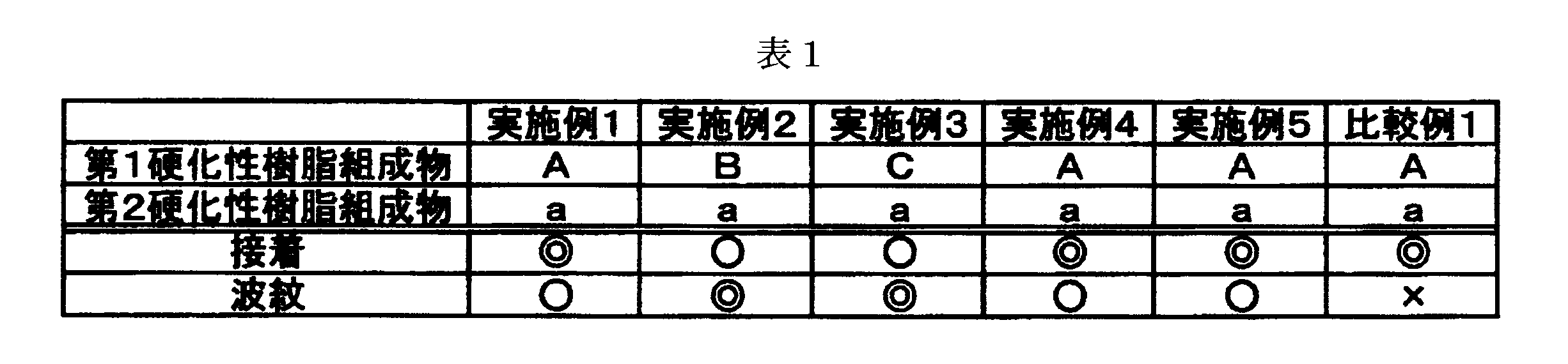
厚さ1mmのスライドガラス2枚を用意し、そのうちの1枚に得られた硬化性樹脂組成物の膜厚が200μmとなるように塗布した。その塗布面に他方のスライドガラスを貼り合わせた。ガラス越しに高圧水銀灯(80W/cm、オゾンレス)で積算光量2000mJ/cm2の紫外線を該樹脂組成物に照射した。硬化物の硬化状態を確認したところ完全に硬化していた。
フッ素系離型剤を塗布した厚さ1mmのスライドガラス2枚を用意し、そのうち1枚の離型剤塗布面に、得られた硬化性樹脂組成物を膜厚が200μmとなるよう塗布した。その後、2枚のスライドガラスを、それぞれの離型剤塗布面が互いに向かい合うように貼り合わせた。ガラス越しに高圧水銀灯(80W/cm、オゾンレス)で積算光量2000mJ/cm2の紫外線を該樹脂組成物に照射し、該樹脂組成物を硬化させた。その後、2枚のスライドガラスを剥離し、膜比重測定用の硬化物を作製した。JIS K7112 B法に準拠し、硬化物の比重(DS)を測定した。また、25℃で樹脂組成物の液比重(DL)を測定した。DS及びDLの測定結果から、次式より硬化収縮率を算出したところ、2.5%未満であった。
硬化収縮率(%)=(DS-DL)÷DS×100
厚さ0.8mmのスライドガラスと厚さ0.8mmのアクリル板を用意し、一方に得られた硬化性樹脂組成物を膜厚が200μmとなるように塗布した後、その塗布面に他方を貼り合わせた。ガラス越しに、高圧水銀灯(80W/cm、オゾンレス)で積算光量2000mJ/cm2の紫外線を該樹脂組成物に照射し、該樹脂組成物を硬化させ、接着性評価用サンプルを作製した。これを、85℃、85%RH環境下、250時間放置した。その評価用サンプルにおいて、目視にてスライドガラス又はアクリル板の樹脂硬化物からの剥がれを確認したが、剥がれはなかった。
得られた硬化性樹脂組成物を充分に硬化させ、JIS K7215に準拠する方法により、デュロメータ硬度計(タイプE)を用いてデュロメータE硬さを測定し、柔軟性を評価した。より具体的には、硬化性樹脂組成物を膜厚が1cmとなるように円柱状の型に流し込み、紫外線を照射して該樹脂組成物を十分に硬化させた。得られた硬化物の硬度をデュロメータ硬度計(タイプE)で測定した。その結果、測定値は10未満であり、柔軟性に優れていた。
フッ素系離型剤を塗布した厚さ40μmのPETフィルム2枚を用意し、そのうちの1枚の離型剤塗布面に、得られた硬化性樹脂組成物を硬化後の膜厚が600μmとなるように塗布した。その後、2枚のPETフィルムを、それぞれの離型剤塗布面が互いに向かい合うように貼り合わせた。PETフィルム越しに高圧水銀灯(80W/cm、オゾンレス)で積算光量2000mJ/cm2の紫外線照射し、該樹脂組成物を硬化させた。その後、2枚のPETフィルムを剥離し、剛性率測定用の硬化物を作製した。その後、2枚のPETフィルムを剥離し、剛性率測定用の硬化物を作製する。そして、剛性率については、ARES(TA Instruments)を用いて、20~40℃の温度領域において剛性率を測定できる。
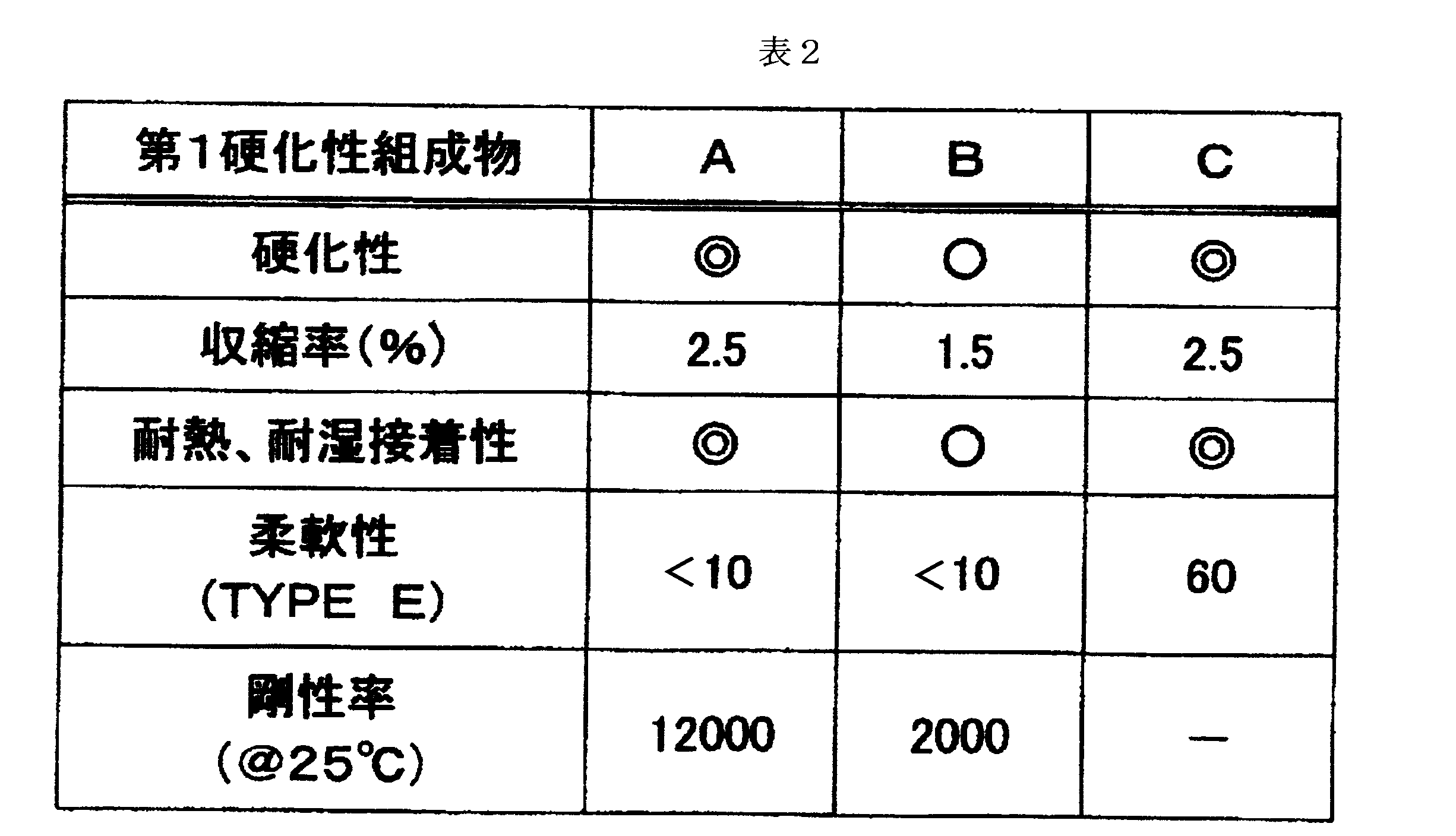
なお、本願は、2015年1月19日付で出願された日本国特許出願(2015-007810)に基づいており、その全体が引用により援用される。また、ここに引用されるすべての参照は全体として取り込まれる。
Claims (12)
- 液晶表示ユニットに保護板を接着した画像表示装置の製造方法であって、
液晶表示ユニットは液晶表示セル、液晶表示セル上に配置された偏光板及び、偏光板を取り囲む前記液晶表示セルを被膜する封止体又は液晶表示セルの周壁部を取り囲むことで液晶表示ユニットを固定する筐体を備え、
(A)前記液晶表示ユニット及び前記保護板の少なくとも一方に、未硬化時に流動性を有する第1硬化性樹脂組成物を塗布する塗布工程と、
(B)前記第1硬化性樹脂組成物を介して前記液晶表示ユニットおよび前記保護板を貼合わせる貼合わせ工程と、を含み、
前記工程(B)の後に下記工程(C-I)~(C-III)の工程を含む画像表示装置の製造方法。
(C-I)前記第1硬化性樹脂組成物を硬化させて前記液晶表示ユニットおよび前記保護板を接着する第1硬化性樹脂組成物硬化工程
(C-II)液晶表示ユニットと保護板を連結させるように、前記保護板、前記液晶表示セルを被膜する封止体又は液晶表示ユニットを固定する筐体、の外周側面部に第2硬化性樹脂組成物を塗布する塗布工程
(C-III)前記工程(C-II)の後に、前記第2硬化性樹脂組成物を硬化して、前記保護板、前記液晶表示セルを被膜する封止体又は液晶表示ユニットを固定する筐体の外周側面部に硬化物層を設ける工程 - (A)前記保護板の表面上に前記第1硬化性樹脂組成物を塗布して硬化又は未硬化の塗布膜を形成し、
(B)前記塗布膜が形成された保護板と液晶表示ユニットを貼合わせ、
(C-II)前記液晶表示ユニットの前記封止体又は液晶表示ユニットを固定する筐体の外周側面部に前記第2硬化性組成物を塗布して硬化又は未硬化の塗布膜を形成する請求項1に記載の画像表示装置の製造方法。 - 前記第1硬化性樹脂組成物の塗布膜の平均厚みが、前記第2硬化性樹脂組成物の塗布膜の平均厚み以下であることを特徴とする請求項1又は請求項2に記載の画像表示装置の製造方法。
- 前記保護板が、遮光部を有する透明ガラス基板、遮光部を有する透明樹脂基板、遮光部と透明電極が形成されたガラス基板、及び、遮光部を有する透明基板に透明電極が形成されたガラス基板またはフィルムが貼りあわされた基板の群から選ばれる1種以上からなる請求項1~3のいずれか一項に記載の画像表示装置の製造方法。
- 前記保護板が、タッチパネルである請求項1~4のいずれか一項に記載の画像表示装置の製造方法。
- 請求項1~5のいずれか一項に記載の画像表示装置の製造方法の、前記第1硬化性樹脂組成物又は前記第2硬化性樹脂組成物用の、(メタ)アクリレート(A)及び光重合開始剤(B)を含有する硬化性樹脂組成物。
- (メタ)アクリレート(A)が、ウレタン(メタ)アクリレート、ポリイソプレン骨格を有する(メタ)アクリレート、ポリブタジエン骨格を有する(メタ)アクリレート及び(メタ)アクリレートモノマーからなる群から選ばれる1種以上である請求項6に記載の硬化性樹脂組成物。
- アセトニトリル又はメタノール中で測定した光重合開始剤(B)のモル吸光係数が、302nm又は313nmでは300ml/(g・cm)以上であり、365nmでは100ml/(g・cm)以下である請求項6又は請求項7に記載の硬化性樹脂組成物。
- 前記第1硬化性樹脂組成物が紫外線を照射した際の硬化率80%における樹脂層の25℃における貯蔵剛性率に対して、紫外線を照射した際の硬化率98%における樹脂層の貯蔵剛性率が3~20倍である樹脂組成物であって、硬化率80%における貯蔵剛性率(25℃)が1×10²Pa~1×10⁵Paである請求項6~8のいずれか一項に記載の硬化性樹脂組成物。
- 請求項1~5のいずれか一項に記載の画像表示装置の製造方法によって得られるタッチパネル。
- 液晶表示ユニットに保護板を接着した画像表示装置であって、
液晶表示ユニットは液晶表示セル、液晶表示セル上に配置された偏光板及び、偏光板を取り囲む前記液晶表示セルを被膜する封止体又は液晶表示セルの周壁部を取り囲むことで液晶表示ユニットを固定する筐体、を備え、
前記偏光板上に形成された第1硬化性樹脂組成物を硬化して得られる第1硬化物層と、
前記保護板、前記液晶表示セルを被膜する封止体又は液晶表示部材を固定する筐体の外周側面部に、前記液晶表示ユニットと保護板を連結させる第2硬化性樹脂組成物を硬化して得られる第2硬化物層とを有する画像表示装置。 - 前記第1硬化性樹脂組成物及び前記第2硬化性樹脂組成物が、ウレタン(メタ)アクリレート化合物、ポリイソプレン骨格を有する(メタ)アクリレート化合物及びポリブタジエン骨格を有する(メタ)アクリレート化合物からなる群から選択される少なくとも1種の(メタ)アクリレート化合物、並びに光重合開始剤を含有している硬化性樹脂組成物である、請求項11に記載の画像表示装置。
Priority Applications (3)
| Application Number | Priority Date | Filing Date | Title |
|---|---|---|---|
| CN201680006333.2A CN107209410B (zh) | 2015-01-19 | 2016-01-19 | 图像显示装置的制造方法、用于该方法的固化性树脂组合物、触控面板和图像显示装置 |
| JP2016570637A JP6633548B2 (ja) | 2015-01-19 | 2016-01-19 | 画像表示装置の製造方法、それに用いる硬化性樹脂組成物、タッチパネル及び画像表示装置 |
| KR1020177020116A KR20170105523A (ko) | 2015-01-19 | 2016-01-19 | 화상 표시 장치의 제조 방법, 그것에 사용하는 경화성 수지 조성물, 터치 패널 및 화상 표시 장치 |
Applications Claiming Priority (2)
| Application Number | Priority Date | Filing Date | Title |
|---|---|---|---|
| JP2015007810 | 2015-01-19 | ||
| JP2015-007810 | 2015-01-19 |
Publications (1)
| Publication Number | Publication Date |
|---|---|
| WO2016117526A1 true WO2016117526A1 (ja) | 2016-07-28 |
Family
ID=56417070
Family Applications (1)
| Application Number | Title | Priority Date | Filing Date |
|---|---|---|---|
| PCT/JP2016/051357 Ceased WO2016117526A1 (ja) | 2015-01-19 | 2016-01-19 | 画像表示装置の製造方法、それに用いる硬化性樹脂組成物、タッチパネル及び画像表示装置 |
Country Status (5)
| Country | Link |
|---|---|
| JP (1) | JP6633548B2 (ja) |
| KR (1) | KR20170105523A (ja) |
| CN (1) | CN107209410B (ja) |
| TW (1) | TW201640193A (ja) |
| WO (1) | WO2016117526A1 (ja) |
Cited By (3)
| Publication number | Priority date | Publication date | Assignee | Title |
|---|---|---|---|---|
| CN110111694A (zh) * | 2019-05-22 | 2019-08-09 | 上海中航光电子有限公司 | 一种柔性显示模组及显示装置 |
| JP2019179791A (ja) * | 2018-03-30 | 2019-10-17 | ミネベアミツミ株式会社 | モジュールの製造方法及び光学モジュールの製造方法 |
| WO2021020295A1 (ja) * | 2019-07-29 | 2021-02-04 | デクセリアルズ株式会社 | 光学装置の製造方法 |
Families Citing this family (2)
| Publication number | Priority date | Publication date | Assignee | Title |
|---|---|---|---|---|
| CN110379298B (zh) * | 2019-07-19 | 2021-06-01 | 深圳市华星光电半导体显示技术有限公司 | 框胶结构和显示面板的制作方法 |
| TWI800461B (zh) * | 2022-09-07 | 2023-04-21 | 達擎股份有限公司 | 電子裝置 |
Citations (4)
| Publication number | Priority date | Publication date | Assignee | Title |
|---|---|---|---|---|
| JP2001066575A (ja) * | 1999-06-22 | 2001-03-16 | Sony Corp | 液晶表示装置の防塵ガラス接合方法 |
| JP2008158251A (ja) * | 2006-12-25 | 2008-07-10 | Hitachi Displays Ltd | 表示装置の製造方法 |
| WO2013131106A1 (en) * | 2012-03-02 | 2013-09-06 | Microsoft Corporation | Support for an optically bonded display device |
| JP2013228748A (ja) * | 2010-12-08 | 2013-11-07 | Asahi Glass Co Ltd | 表示装置 |
Family Cites Families (3)
| Publication number | Priority date | Publication date | Assignee | Title |
|---|---|---|---|---|
| JP4711354B2 (ja) * | 2007-07-17 | 2011-06-29 | ソニーケミカル&インフォメーションデバイス株式会社 | 画像表示装置の製造方法 |
| JP2012216678A (ja) * | 2011-03-31 | 2012-11-08 | Fujitsu Ltd | 電子部品、電子機器、及びはんだペースト |
| WO2013105163A1 (ja) * | 2012-01-13 | 2013-07-18 | 日本化薬株式会社 | 光学部材及びその製造に用いる紫外線硬化型接着剤 |
-
2016
- 2016-01-19 TW TW105101647A patent/TW201640193A/zh unknown
- 2016-01-19 JP JP2016570637A patent/JP6633548B2/ja active Active
- 2016-01-19 KR KR1020177020116A patent/KR20170105523A/ko not_active Withdrawn
- 2016-01-19 CN CN201680006333.2A patent/CN107209410B/zh not_active Expired - Fee Related
- 2016-01-19 WO PCT/JP2016/051357 patent/WO2016117526A1/ja not_active Ceased
Patent Citations (4)
| Publication number | Priority date | Publication date | Assignee | Title |
|---|---|---|---|---|
| JP2001066575A (ja) * | 1999-06-22 | 2001-03-16 | Sony Corp | 液晶表示装置の防塵ガラス接合方法 |
| JP2008158251A (ja) * | 2006-12-25 | 2008-07-10 | Hitachi Displays Ltd | 表示装置の製造方法 |
| JP2013228748A (ja) * | 2010-12-08 | 2013-11-07 | Asahi Glass Co Ltd | 表示装置 |
| WO2013131106A1 (en) * | 2012-03-02 | 2013-09-06 | Microsoft Corporation | Support for an optically bonded display device |
Cited By (6)
| Publication number | Priority date | Publication date | Assignee | Title |
|---|---|---|---|---|
| JP2019179791A (ja) * | 2018-03-30 | 2019-10-17 | ミネベアミツミ株式会社 | モジュールの製造方法及び光学モジュールの製造方法 |
| JP7136532B2 (ja) | 2018-03-30 | 2022-09-13 | ミネベアミツミ株式会社 | モジュールの製造方法及び光学モジュールの製造方法 |
| CN110111694A (zh) * | 2019-05-22 | 2019-08-09 | 上海中航光电子有限公司 | 一种柔性显示模组及显示装置 |
| WO2021020295A1 (ja) * | 2019-07-29 | 2021-02-04 | デクセリアルズ株式会社 | 光学装置の製造方法 |
| JP2021021859A (ja) * | 2019-07-29 | 2021-02-18 | デクセリアルズ株式会社 | 光学装置の製造方法 |
| JP7274966B2 (ja) | 2019-07-29 | 2023-05-17 | デクセリアルズ株式会社 | 光学装置の製造方法 |
Also Published As
| Publication number | Publication date |
|---|---|
| TW201640193A (zh) | 2016-11-16 |
| KR20170105523A (ko) | 2017-09-19 |
| CN107209410A (zh) | 2017-09-26 |
| CN107209410B (zh) | 2021-03-30 |
| JPWO2016117526A1 (ja) | 2017-10-26 |
| JP6633548B2 (ja) | 2020-01-22 |
Similar Documents
| Publication | Publication Date | Title |
|---|---|---|
| JP6326390B2 (ja) | 紫外線硬化型樹脂組成物 | |
| JP5331271B1 (ja) | 光学部材の製造方法及びそのための紫外線硬化型樹脂組成物の使用 | |
| WO2015119245A1 (ja) | タッチパネル用紫外線硬化型接着剤組成物、それを用いた光学部材の製造方法、硬化物及びタッチパネル | |
| JP6778106B2 (ja) | タッチパネル用紫外線硬化型樹脂組成物、それを用いた貼り合せ方法及び物品 | |
| JP6620092B2 (ja) | タッチパネル用紫外線硬化型樹脂組成物、それを用いた貼り合せ方法及び物品 | |
| WO2015199156A1 (ja) | 光学部材の製造方法及びそれに用いる紫外線硬化型樹脂組成物 | |
| JPWO2015190561A1 (ja) | タッチパネル用紫外線硬化型樹脂組成物、それを用いた貼り合せ方法及び物品 | |
| JP6378184B2 (ja) | 光学部材の製造方法及びそれに用いる紫外線硬化型樹脂組成物 | |
| JP6633548B2 (ja) | 画像表示装置の製造方法、それに用いる硬化性樹脂組成物、タッチパネル及び画像表示装置 | |
| JP6353908B2 (ja) | 光学部材の製造方法及びそれに用いる硬化性樹脂組成物 | |
| JP6499406B2 (ja) | 光学部材の製造方法及びそれに用いる硬化性樹脂組成物 | |
| JPWO2015190571A1 (ja) | タッチパネル用紫外線硬化型樹脂組成物、それを用いた貼り合せ方法及び物品 | |
| WO2019016963A1 (ja) | 紫外線硬化型接着剤、それを用いた貼り合せ方法及び物品 | |
| WO2017073584A1 (ja) | タッチパネル用紫外線硬化型樹脂組成物、それを用いた硬化物及びタッチパネル | |
| JP2018012750A (ja) | 紫外線硬化型接着剤、それを用いた貼り合せ方法及び物品 |
Legal Events
| Date | Code | Title | Description |
|---|---|---|---|
| 121 | Ep: the epo has been informed by wipo that ep was designated in this application |
Ref document number: 16740133 Country of ref document: EP Kind code of ref document: A1 |
|
| ENP | Entry into the national phase |
Ref document number: 2016570637 Country of ref document: JP Kind code of ref document: A |
|
| ENP | Entry into the national phase |
Ref document number: 20177020116 Country of ref document: KR Kind code of ref document: A |
|
| NENP | Non-entry into the national phase |
Ref country code: DE |
|
| 122 | Ep: pct application non-entry in european phase |
Ref document number: 16740133 Country of ref document: EP Kind code of ref document: A1 |