WO2016111216A1 - Organic electroluminescent device, organic-electroluminescent-device driving method, and illumination device - Google Patents
Organic electroluminescent device, organic-electroluminescent-device driving method, and illumination device Download PDFInfo
- Publication number
- WO2016111216A1 WO2016111216A1 PCT/JP2015/086461 JP2015086461W WO2016111216A1 WO 2016111216 A1 WO2016111216 A1 WO 2016111216A1 JP 2015086461 W JP2015086461 W JP 2015086461W WO 2016111216 A1 WO2016111216 A1 WO 2016111216A1
- Authority
- WO
- WIPO (PCT)
- Prior art keywords
- organic electroluminescence
- current
- substituted
- bond
- ring
- Prior art date
Links
- ZFGVQDSHPXLWKY-UHFFFAOYSA-N CC(CC=C1)C=C1P(c1ccccc1)(c(cccc1)c1Oc1ccccc1P(c1ccccc1)(C1=CCCC=C1)=O)=O Chemical compound CC(CC=C1)C=C1P(c1ccccc1)(c(cccc1)c1Oc1ccccc1P(c1ccccc1)(C1=CCCC=C1)=O)=O ZFGVQDSHPXLWKY-UHFFFAOYSA-N 0.000 description 1
- QMTOKTGMPXIEQA-UHFFFAOYSA-N CC(CC=C1C2(C)C=CC=CC22)C=C1N2c1cccc(-[n]2c(cccc3)c3c3c2cccc3)c1 Chemical compound CC(CC=C1C2(C)C=CC=CC22)C=C1N2c1cccc(-[n]2c(cccc3)c3c3c2cccc3)c1 QMTOKTGMPXIEQA-UHFFFAOYSA-N 0.000 description 1
- VOXZDWNPVJITMN-PAOLREHBSA-N C[C@](CC1)(C(CC2)C(CCc3c4)C1c3ccc4O)[C@H]2O Chemical compound C[C@](CC1)(C(CC2)C(CCc3c4)C1c3ccc4O)[C@H]2O VOXZDWNPVJITMN-PAOLREHBSA-N 0.000 description 1
- ARPMMQCZCWLQRL-PGFDTMBTSA-N C[C@](CCC1)(CC2)C1C(CC1)C2[C@@](C)(CC2)C1CC2[n]1nnc(-c2ccccn2)c1 Chemical compound C[C@](CCC1)(CC2)C1C(CC1)C2[C@@](C)(CC2)C1CC2[n]1nnc(-c2ccccn2)c1 ARPMMQCZCWLQRL-PGFDTMBTSA-N 0.000 description 1
- GRADGEXHAXSWJB-UHFFFAOYSA-N O=P(C1=CC=CCC1)(c1ccccc1)c(cc1c2c3)ccc1[s]c2ccc3P(c1ccccc1)(c1ccccc1)=O Chemical compound O=P(C1=CC=CCC1)(c1ccccc1)c(cc1c2c3)ccc1[s]c2ccc3P(c1ccccc1)(c1ccccc1)=O GRADGEXHAXSWJB-UHFFFAOYSA-N 0.000 description 1
Images


Classifications
-
- C—CHEMISTRY; METALLURGY
- C07—ORGANIC CHEMISTRY
- C07J—STEROIDS
- C07J43/00—Normal steroids having a nitrogen-containing hetero ring spiro-condensed or not condensed with the cyclopenta(a)hydrophenanthrene skeleton
- C07J43/003—Normal steroids having a nitrogen-containing hetero ring spiro-condensed or not condensed with the cyclopenta(a)hydrophenanthrene skeleton not condensed
-
- C—CHEMISTRY; METALLURGY
- C07—ORGANIC CHEMISTRY
- C07J—STEROIDS
- C07J31/00—Normal steroids containing one or more sulfur atoms not belonging to a hetero ring
- C07J31/006—Normal steroids containing one or more sulfur atoms not belonging to a hetero ring not covered by C07J31/003
-
- C—CHEMISTRY; METALLURGY
- C07—ORGANIC CHEMISTRY
- C07J—STEROIDS
- C07J41/00—Normal steroids containing one or more nitrogen atoms not belonging to a hetero ring
- C07J41/0005—Normal steroids containing one or more nitrogen atoms not belonging to a hetero ring the nitrogen atom being directly linked to the cyclopenta(a)hydro phenanthrene skeleton
- C07J41/0027—Azides
Landscapes
- Chemical & Material Sciences (AREA)
- Organic Chemistry (AREA)
- Health & Medical Sciences (AREA)
- General Health & Medical Sciences (AREA)
- Electroluminescent Light Sources (AREA)
- Steroid Compounds (AREA)
Abstract
In this organic electroluminescent device, which has a luminescent layer containing π-conjugated molecules, when the application of a current is stopped after the current is applied, light is emitted while the current is being applied and also after the application of the current is stopped.
Description
本発明は、有機エレクトロルミネッセンス素子、有機エレクトロルミネッセンス素子の駆動方法および照明装置に関し、特に蓄光機能を有する有機エレクトロルミネッセンス素子に関する。
The present invention relates to an organic electroluminescence element, a driving method of an organic electroluminescence element, and a lighting device, and particularly relates to an organic electroluminescence element having a light storage function.
有機エレクトロルミネッセンス素子(有機EL素子)などの有機発光素子に様々な性能を付与し、各種用途に応用することや、新たな用途を開発する試みが盛んに行われている。
例えば、発光材料が放射する光には大別して蛍光とリン光があり、このうちリン光は、光励起による発光の場合、発光材料に励起光が照射されている間は蓄光し、励起光の照射が停止された後に発光する蓄光現象を見られることが知られている。この蓄光現象を有機発光素子に利用すれば、エネルギーの印加を停止した後にも発光が残る、蓄光照明等が実現するものと考えられる。しかしながら、電流励起により発光を生じさせる有機エレクトロルミネッセンス素子については、このような蓄光現象が観測されたという報告はなされていない。
例えば、非特許文献1には、蛍光材料を発光材料とする有機エレクトロルミネッセンス素子をパルス駆動させてリン光スペクトルを観測したことが報告されている。しかし、この有機エレクトロルミネッセンス素子でリン光が観測されているのは、電流を印加しているオン期間のみであり、電流の印加を停止したオフ期間でのリン光の放射は確認されていない。 Various attempts have been made to give various performances to organic light-emitting elements such as organic electroluminescence elements (organic EL elements) and to apply them to various uses, and to develop new uses.
For example, light emitted from a luminescent material can be broadly classified into fluorescence and phosphorescence. Of these, phosphorescence is stored when excitation light is applied to the luminescent material in the case of light emission by photoexcitation. It is known that a phosphorescent phenomenon in which light is emitted after the light is stopped can be seen. If this phosphorescence phenomenon is used for an organic light emitting device, it is considered that phosphorescence illumination or the like in which light emission remains even after the application of energy is stopped is realized. However, there has been no report that such a phosphorescent phenomenon has been observed for an organic electroluminescence element that emits light by current excitation.
For example, Non-PatentDocument 1 reports that a phosphorescent spectrum was observed by driving an organic electroluminescence element using a fluorescent material as a light-emitting material in a pulsed manner. However, phosphorescence is observed in this organic electroluminescence element only in the on period in which the current is applied, and no phosphorescence is emitted in the off period in which the current application is stopped.
例えば、発光材料が放射する光には大別して蛍光とリン光があり、このうちリン光は、光励起による発光の場合、発光材料に励起光が照射されている間は蓄光し、励起光の照射が停止された後に発光する蓄光現象を見られることが知られている。この蓄光現象を有機発光素子に利用すれば、エネルギーの印加を停止した後にも発光が残る、蓄光照明等が実現するものと考えられる。しかしながら、電流励起により発光を生じさせる有機エレクトロルミネッセンス素子については、このような蓄光現象が観測されたという報告はなされていない。
例えば、非特許文献1には、蛍光材料を発光材料とする有機エレクトロルミネッセンス素子をパルス駆動させてリン光スペクトルを観測したことが報告されている。しかし、この有機エレクトロルミネッセンス素子でリン光が観測されているのは、電流を印加しているオン期間のみであり、電流の印加を停止したオフ期間でのリン光の放射は確認されていない。 Various attempts have been made to give various performances to organic light-emitting elements such as organic electroluminescence elements (organic EL elements) and to apply them to various uses, and to develop new uses.
For example, light emitted from a luminescent material can be broadly classified into fluorescence and phosphorescence. Of these, phosphorescence is stored when excitation light is applied to the luminescent material in the case of light emission by photoexcitation. It is known that a phosphorescent phenomenon in which light is emitted after the light is stopped can be seen. If this phosphorescence phenomenon is used for an organic light emitting device, it is considered that phosphorescence illumination or the like in which light emission remains even after the application of energy is stopped is realized. However, there has been no report that such a phosphorescent phenomenon has been observed for an organic electroluminescence element that emits light by current excitation.
For example, Non-Patent
そこで、本発明者らは、蓄光機能を有する有機エレクトロルミネッセンス素子を実現するためには、リン光の発光プロセスを考慮した発光材料の選択が重要であると考え、研究を進めた。
すなわち、有機エレクトロルミネッセンス素子では、電流印加によって発光層に注入された正孔と電子が再結合することでエネルギーを生じ、このエネルギーによって発光材料が励起一重項状態と励起三重項状態に励起される。これにより生成された一重項励起子は蛍光を放射しつつ基底状態に戻り、三重項励起子はリン光を放射しつつ基底状態に戻る。こうした有機エレクトロルミネッセンス素子で蓄光現象を発現させるためには、励起三重項状態に励起された発光材料が励起状態で長く留まるとともに、その後、効率良く放射失活することが必要である。しかしながら、非常に多くの発光性の有機化合物が報告されている一方、それらの中から励起三重項状態が長く持続するものを選択する指標は確立されていない。仮に、励起三重項状態が長く持続する有機化合物が選択できたとしても、そのような有機化合物は、励起状態にある間に熱運動によって無放射失活する機会が多くなるため、通常は室温でリン光を放射させることは難しい。特に、有機エレクトロルミネッセンス素子では、電流密度が高くなると三重項-三重項消滅が起きるため、リン光を利用することが一層難しいものになっている。このような理由から、蓄光機能を有する有機エレクトロルミネッセンス素子の実現は、半ば不可能であるとされており、全く検討がなされていないのが実情である。
このような状況下において本発明者らは、蓄光機能を有する有機エレクトロルミネッセンス素子を提供することを目的として、励起三重項状態が比較的長く持続すると考えられた種々の有機化合物について、電流励起による蓄光現象の有無を評価する試験を網羅的に行う検討を進めた。 Therefore, the present inventors considered that selection of a light emitting material in consideration of a phosphorescent light emitting process is important in order to realize an organic electroluminescence element having a phosphorescent function, and proceeded with research.
That is, in an organic electroluminescence element, energy is generated by recombination of holes and electrons injected into the light-emitting layer by application of current, and the light-emitting material is excited to an excited singlet state and an excited triplet state by this energy. . The singlet excitons generated thereby return to the ground state while emitting fluorescence, and the triplet excitons return to the ground state while emitting phosphorescence. In order for the organic electroluminescence element to exhibit the phosphorescence phenomenon, it is necessary that the light emitting material excited in the excited triplet state stays in the excited state for a long time and then efficiently deactivates the radiation. However, while an extremely large number of light-emitting organic compounds have been reported, no indicator has been established for selecting one in which the excited triplet state lasts long. Even if an organic compound in which the excited triplet state persists for a long time can be selected, such an organic compound has a greater chance of non-radiative deactivation due to thermal motion while in the excited state. It is difficult to emit phosphorescence. In particular, in organic electroluminescence devices, triplet-triplet annihilation occurs when the current density increases, making it more difficult to use phosphorescence. For these reasons, it is considered that the realization of an organic electroluminescence element having a phosphorescent function is impossible, and the fact is that no investigation has been made.
Under such circumstances, the inventors of the present invention aimed to provide an organic electroluminescence device having a phosphorescent function, with respect to various organic compounds whose excited triplet state was considered to be maintained for a relatively long time by current excitation. A comprehensive study was conducted to evaluate the presence or absence of the phosphorescent phenomenon.
鋭意検討を進めた結果、本発明者らは、発光材料として、π共役性平面分子を用いることにより、電流を印加している間と電流の印加を停止した後の両方で発光する、蓄光型の有機エレクトロルミネッセンス素子が実現することを見出した。具体的に、本発明は、以下の構成を有する。
[1] 一対の電極と、該一対の電極同士の間に発光層を含む少なくとも1層の有機層とを有し、
前記発光層は、π共役性平面分子を含み、前記一対の電極により、前記発光層に電流を印加した後に電流の印加を停止したとき、電流を印加している間と電流の印加を停止した後の両方で発光することを特徴とする有機エレクトロルミネッセンス素子。
[2] 電流を印加している間に蛍光を発光し、電流の印加を停止した後にリン光または遅延蛍光を発光することを特徴とする[1]に記載の有機エレクトロルミネッセンス素子。
[3] 前記π共役性平面分子は、少なくとも1つの芳香環を有することを特徴とする[1]または[2]に記載の有機エレクトロルミネッセンス素子。
[4] 前記芳香環は、ベンゼン環または2つ以上のベンゼン環が縮合した縮合多環構造の芳香環であることを特徴とする[3]に有機エレクトロルミネッセンス素子。
[5] 前記π共役性平面分子は、水素原子の一部または全部が2H(デューテリウムD)で置換されたD置換体であることを特徴とする[1]~[4]のいずれか1項に記載の有機エレクトロルミネッセンス素子。
[6] 前記π共役性平面分子は、π共役系を構成する原子団にアミノ基が置換した構造を有する2級アミンまたは3級アミンであることを特徴とする[1]~[5]のいずれか1項に記載の有機エレクトロルミネッセンス素子。
[7] 前記アミノ基は、置換もしくは無置換のジアリールアミノ基および置換もしくは無置換のジアルキルアミノ基の少なくとも一方であることを特徴とする[6]に記載の有機エレクトロルミネッセンス素子。
[8] 前記π共役性平面分子は、置換もしくは無置換のフルオレン環を有することを特徴とする[1]~[7]のいずれか1項に記載の有機エレクトロルミネッセンス素子。
[9] 前記π共役性平面分子は、下記式で表される化合物、下記式で表される化合物の水素原子の少なくとも1つが置換基で置換された誘導体、または、前記記合物もしくは前記誘導体の水素原子の一部または全部が2H(デューテリウムD)で置換されたD置換体であることを特徴とする[1]~[8]のいずれか1項に記載の有機エレクトロルミネッセンス素子。

[10] 前記発光層は、さらにホスト材料を含むことを特徴とする[1]~[9]のいずれか1項に記載の有機エレクトロルミネッセンス素子。
[11] 前記ホスト材料の最低励起三重項エネルギー準位が、前記π共役性平面分子の最低励起三重項エネルギー準位よりも0.1eV以上高いことを特徴とする[10]に記載の有機エレクトロルミネッセンス素子。
[12] 前記ホスト材料は、少なくとも2つのシクロアルカンが縮合した環状構造または少なくとも2つのシクロアルカンと少なくとも1つのシクロアルケンが縮合した環状構造と、前記環状構造に置換した置換もしくは無置換のカルバゾリル基および置換もしくは無置換のジアリールアミノ基の少なくとも一方を有する化合物であることを特徴とする[10]または[11]に記載の有機エレクトロルミネッセンス素子。
[13] 前記置換基は、置換もしくは無置換のカルバゾリル基であることを特徴とする[12]に記載の有機エレクトロルミネッセンス素子。
[14] 前記ホスト材料は、下記一般式(1)で表される化合物であることを特徴とする[10]~[13]のいずれか1項に記載の有機エレクトロルミネッセンス素子。

[一般式(1)において、Arは少なくとも1つの芳香環を有する置換基を表し、mは1~5のいずれかの整数を表し、ZはAr以外の置換基を表し、nは0~21のいずれかの整数を表す。mが2以上であるとき、m個のArは互いに同一であっても異なっていてもよい。Arの結合位置は、アンドロスタン環を構成する4つの環のいずれであってもよい。また、nが2以上であるとき、n個のZは互いに同一であっても異なっていてもよい。Zの結合位置は、アンドロスタン環を構成する4つの環のいずれであってもよい。アンドロスタン環の1位と2位の結合、2位と3位の結合、3位と4位の結合、6位と7位の結合、11位と12位の結合、15位と16位の結合および16位と17位の結合からなる群より選択される1以上の結合は二重結合であってもよい。ただし、1位と2位の結合と2位と3位の結合、2位と3位の結合と3位と4位の結合、および15位と16位の結合と16位と17位の結合が、それぞれ同時に二重結合となることはない。]
[15] [1]~[14]のいずれか1項に記載の有機エレクトロルミネッセンス素子を駆動する駆動方法であって、前記一対の電極により、前記発光層に電流を印加した後に電流の印加を停止して、電流を印加している間と電流の印加を停止した後の両方で発光を生じさせることを特徴とする有機エレクトロルミネッセンス素子の駆動方法。
[16] 前記発光層に電流を印加する時間が1μ秒以上であることを特徴とする[15]に記載の有機エレクトロルミネッセンス素子の駆動方法。
[17] 前記発光層に、電流を印加するオン期間と電流の印加を停止するオフ期間を交互に繰り返すパルス状のパターンで電流を印加することを特徴とする[15]または[16]に記載の有機エレクトロルミネッセンス素子の駆動方法。
[18] 前記オン期間が1μ秒~10秒であり、前記オフ期間が1μ秒~10分であることを特徴とする[17]に記載の有機エレクトロルミネッセンス素子の駆動方法。
[19] [1]~[14]のいずれか1項に記載の有機エレクトロルミネッセンス素子を有することを特徴とする照明装置。
[20] 電流を印加するオン期間と電流の印加を停止するオフ期間を交互に繰り返すパルス状のパターンで前記発光層に電流を印加するように有機エレクトロルミネッセンス素子を制御する制御手段を有することを特徴とする[19]に記載の照明装置。
[21] 上記一般式(1)で表される化合物。 As a result of diligent investigation, the present inventors have used a π-conjugated planar molecule as a luminescent material, so that the phosphorescent type emits light both during and after the application of current. It was found that the organic electroluminescence device of the present invention was realized. Specifically, the present invention has the following configuration.
[1] having a pair of electrodes and at least one organic layer including a light emitting layer between the pair of electrodes,
The light emitting layer includes a π-conjugated planar molecule, and when the application of current is stopped after applying a current to the light emitting layer by the pair of electrodes, the application of the current is stopped while applying the current. An organic electroluminescence element characterized by emitting light later.
[2] The organic electroluminescence device according to [1], wherein fluorescence is emitted while an electric current is applied, and phosphorescence or delayed fluorescence is emitted after the application of the current is stopped.
[3] The organic electroluminescence device according to [1] or [2], wherein the π-conjugated planar molecule has at least one aromatic ring.
[4] The organic electroluminescence device according to [3], wherein the aromatic ring is a benzene ring or an aromatic ring having a condensed polycyclic structure in which two or more benzene rings are condensed.
[5] Any one of [1] to [4], wherein the π-conjugated planar molecule is a D-substituted product in which part or all of hydrogen atoms are substituted with 2 H (deuterium D). 2. The organic electroluminescence device according toitem 1.
[6] The π-conjugated planar molecule is a secondary amine or a tertiary amine having a structure in which an amino group is substituted for an atomic group constituting a π-conjugated system. [1] to [5] The organic electroluminescent element of any one of Claims.
[7] The organic electroluminescence device according to [6], wherein the amino group is at least one of a substituted or unsubstituted diarylamino group and a substituted or unsubstituted dialkylamino group.
[8] The organic electroluminescence device according to any one of [1] to [7], wherein the π-conjugated planar molecule has a substituted or unsubstituted fluorene ring.
[9] The π-conjugated planar molecule is a compound represented by the following formula, a derivative in which at least one hydrogen atom of the compound represented by the following formula is substituted with a substituent, or the compound or the derivative The organic electroluminescence device according to any one of [1] to [8], wherein a part or all of the hydrogen atoms in the compound is a D-substituted product in which 2 H (deuterium D) is substituted.
[10] The organic electroluminescent element according to any one of [1] to [9], wherein the light emitting layer further includes a host material.
[11] The organic electro according to [10], wherein the lowest excited triplet energy level of the host material is 0.1 eV or more higher than the lowest excited triplet energy level of the π-conjugated planar molecule. Luminescence element.
[12] The host material includes a cyclic structure in which at least two cycloalkanes are condensed, a cyclic structure in which at least two cycloalkanes and at least one cycloalkene are condensed, and a substituted or unsubstituted carbazolyl group substituted in the cyclic structure. And [10] or [11], wherein the organic electroluminescence device is a compound having at least one of a substituted or unsubstituted diarylamino group.
[13] The organic electroluminescence device according to [12], wherein the substituent is a substituted or unsubstituted carbazolyl group.
[14] The organic electroluminescence device according to any one of [10] to [13], wherein the host material is a compound represented by the following general formula (1).
[In the general formula (1), Ar represents a substituent having at least one aromatic ring, m represents an integer of 1 to 5, Z represents a substituent other than Ar, and n represents 0 to 21. Represents any integer. When m is 2 or more, m Ar may be the same or different from each other. Ar may be bonded to any of the four rings constituting the androstane ring. When n is 2 or more, the n Zs may be the same as or different from each other. The bonding position of Z may be any of the four rings constituting the androstane ring. Bonds at the 1st and 2nd positions of the androstane ring, 2nd and 3rd positions, 3rd and 4th positions, 6th and 7th positions, 11th and 12th positions, 15th and 16th positions The bond and the one or more bonds selected from the group consisting of the 16-position and 17-position bonds may be double bonds. However, the 1st and 2nd bond, the 2nd and 3rd bond, the 2nd and 3rd bond, the 3rd and 4th bond, and the 15th and 16th bond and the 16th and 17th bond However, they are not simultaneously double bonds. ]
[15] A driving method for driving the organic electroluminescence device according to any one of [1] to [14], wherein the current is applied to the light emitting layer after the current is applied to the light emitting layer by the pair of electrodes. A method for driving an organic electroluminescence element, characterized in that light emission is generated both while the current is applied and after the current application is stopped.
[16] The method for driving an organic electroluminescence element according to [15], wherein a time for applying a current to the light emitting layer is 1 μsec or more.
[17] The current described in [15] or [16], wherein the current is applied to the light emitting layer in a pulsed pattern in which an on period in which current is applied and an off period in which current application is stopped are alternately repeated. Driving method of the organic electroluminescence element.
[18] The organic electroluminescence element driving method according to [17], wherein the on period is 1 μs to 10 seconds and the off period is 1 μs to 10 minutes.
[19] An illumination device comprising the organic electroluminescent element according to any one of [1] to [14].
[20] It has control means for controlling the organic electroluminescence element so as to apply a current to the light emitting layer in a pulsed pattern in which an on period in which current is applied and an off period in which application of current is stopped are alternately repeated. The lighting device according to [19], which is characterized.
[21] A compound represented by the general formula (1).
[1] 一対の電極と、該一対の電極同士の間に発光層を含む少なくとも1層の有機層とを有し、
前記発光層は、π共役性平面分子を含み、前記一対の電極により、前記発光層に電流を印加した後に電流の印加を停止したとき、電流を印加している間と電流の印加を停止した後の両方で発光することを特徴とする有機エレクトロルミネッセンス素子。
[2] 電流を印加している間に蛍光を発光し、電流の印加を停止した後にリン光または遅延蛍光を発光することを特徴とする[1]に記載の有機エレクトロルミネッセンス素子。
[3] 前記π共役性平面分子は、少なくとも1つの芳香環を有することを特徴とする[1]または[2]に記載の有機エレクトロルミネッセンス素子。
[4] 前記芳香環は、ベンゼン環または2つ以上のベンゼン環が縮合した縮合多環構造の芳香環であることを特徴とする[3]に有機エレクトロルミネッセンス素子。
[5] 前記π共役性平面分子は、水素原子の一部または全部が2H(デューテリウムD)で置換されたD置換体であることを特徴とする[1]~[4]のいずれか1項に記載の有機エレクトロルミネッセンス素子。
[6] 前記π共役性平面分子は、π共役系を構成する原子団にアミノ基が置換した構造を有する2級アミンまたは3級アミンであることを特徴とする[1]~[5]のいずれか1項に記載の有機エレクトロルミネッセンス素子。
[7] 前記アミノ基は、置換もしくは無置換のジアリールアミノ基および置換もしくは無置換のジアルキルアミノ基の少なくとも一方であることを特徴とする[6]に記載の有機エレクトロルミネッセンス素子。
[8] 前記π共役性平面分子は、置換もしくは無置換のフルオレン環を有することを特徴とする[1]~[7]のいずれか1項に記載の有機エレクトロルミネッセンス素子。
[9] 前記π共役性平面分子は、下記式で表される化合物、下記式で表される化合物の水素原子の少なくとも1つが置換基で置換された誘導体、または、前記記合物もしくは前記誘導体の水素原子の一部または全部が2H(デューテリウムD)で置換されたD置換体であることを特徴とする[1]~[8]のいずれか1項に記載の有機エレクトロルミネッセンス素子。
[11] 前記ホスト材料の最低励起三重項エネルギー準位が、前記π共役性平面分子の最低励起三重項エネルギー準位よりも0.1eV以上高いことを特徴とする[10]に記載の有機エレクトロルミネッセンス素子。
[12] 前記ホスト材料は、少なくとも2つのシクロアルカンが縮合した環状構造または少なくとも2つのシクロアルカンと少なくとも1つのシクロアルケンが縮合した環状構造と、前記環状構造に置換した置換もしくは無置換のカルバゾリル基および置換もしくは無置換のジアリールアミノ基の少なくとも一方を有する化合物であることを特徴とする[10]または[11]に記載の有機エレクトロルミネッセンス素子。
[13] 前記置換基は、置換もしくは無置換のカルバゾリル基であることを特徴とする[12]に記載の有機エレクトロルミネッセンス素子。
[14] 前記ホスト材料は、下記一般式(1)で表される化合物であることを特徴とする[10]~[13]のいずれか1項に記載の有機エレクトロルミネッセンス素子。
[15] [1]~[14]のいずれか1項に記載の有機エレクトロルミネッセンス素子を駆動する駆動方法であって、前記一対の電極により、前記発光層に電流を印加した後に電流の印加を停止して、電流を印加している間と電流の印加を停止した後の両方で発光を生じさせることを特徴とする有機エレクトロルミネッセンス素子の駆動方法。
[16] 前記発光層に電流を印加する時間が1μ秒以上であることを特徴とする[15]に記載の有機エレクトロルミネッセンス素子の駆動方法。
[17] 前記発光層に、電流を印加するオン期間と電流の印加を停止するオフ期間を交互に繰り返すパルス状のパターンで電流を印加することを特徴とする[15]または[16]に記載の有機エレクトロルミネッセンス素子の駆動方法。
[18] 前記オン期間が1μ秒~10秒であり、前記オフ期間が1μ秒~10分であることを特徴とする[17]に記載の有機エレクトロルミネッセンス素子の駆動方法。
[19] [1]~[14]のいずれか1項に記載の有機エレクトロルミネッセンス素子を有することを特徴とする照明装置。
[20] 電流を印加するオン期間と電流の印加を停止するオフ期間を交互に繰り返すパルス状のパターンで前記発光層に電流を印加するように有機エレクトロルミネッセンス素子を制御する制御手段を有することを特徴とする[19]に記載の照明装置。
[21] 上記一般式(1)で表される化合物。 As a result of diligent investigation, the present inventors have used a π-conjugated planar molecule as a luminescent material, so that the phosphorescent type emits light both during and after the application of current. It was found that the organic electroluminescence device of the present invention was realized. Specifically, the present invention has the following configuration.
[1] having a pair of electrodes and at least one organic layer including a light emitting layer between the pair of electrodes,
The light emitting layer includes a π-conjugated planar molecule, and when the application of current is stopped after applying a current to the light emitting layer by the pair of electrodes, the application of the current is stopped while applying the current. An organic electroluminescence element characterized by emitting light later.
[2] The organic electroluminescence device according to [1], wherein fluorescence is emitted while an electric current is applied, and phosphorescence or delayed fluorescence is emitted after the application of the current is stopped.
[3] The organic electroluminescence device according to [1] or [2], wherein the π-conjugated planar molecule has at least one aromatic ring.
[4] The organic electroluminescence device according to [3], wherein the aromatic ring is a benzene ring or an aromatic ring having a condensed polycyclic structure in which two or more benzene rings are condensed.
[5] Any one of [1] to [4], wherein the π-conjugated planar molecule is a D-substituted product in which part or all of hydrogen atoms are substituted with 2 H (deuterium D). 2. The organic electroluminescence device according to
[6] The π-conjugated planar molecule is a secondary amine or a tertiary amine having a structure in which an amino group is substituted for an atomic group constituting a π-conjugated system. [1] to [5] The organic electroluminescent element of any one of Claims.
[7] The organic electroluminescence device according to [6], wherein the amino group is at least one of a substituted or unsubstituted diarylamino group and a substituted or unsubstituted dialkylamino group.
[8] The organic electroluminescence device according to any one of [1] to [7], wherein the π-conjugated planar molecule has a substituted or unsubstituted fluorene ring.
[9] The π-conjugated planar molecule is a compound represented by the following formula, a derivative in which at least one hydrogen atom of the compound represented by the following formula is substituted with a substituent, or the compound or the derivative The organic electroluminescence device according to any one of [1] to [8], wherein a part or all of the hydrogen atoms in the compound is a D-substituted product in which 2 H (deuterium D) is substituted.
[11] The organic electro according to [10], wherein the lowest excited triplet energy level of the host material is 0.1 eV or more higher than the lowest excited triplet energy level of the π-conjugated planar molecule. Luminescence element.
[12] The host material includes a cyclic structure in which at least two cycloalkanes are condensed, a cyclic structure in which at least two cycloalkanes and at least one cycloalkene are condensed, and a substituted or unsubstituted carbazolyl group substituted in the cyclic structure. And [10] or [11], wherein the organic electroluminescence device is a compound having at least one of a substituted or unsubstituted diarylamino group.
[13] The organic electroluminescence device according to [12], wherein the substituent is a substituted or unsubstituted carbazolyl group.
[14] The organic electroluminescence device according to any one of [10] to [13], wherein the host material is a compound represented by the following general formula (1).
[15] A driving method for driving the organic electroluminescence device according to any one of [1] to [14], wherein the current is applied to the light emitting layer after the current is applied to the light emitting layer by the pair of electrodes. A method for driving an organic electroluminescence element, characterized in that light emission is generated both while the current is applied and after the current application is stopped.
[16] The method for driving an organic electroluminescence element according to [15], wherein a time for applying a current to the light emitting layer is 1 μsec or more.
[17] The current described in [15] or [16], wherein the current is applied to the light emitting layer in a pulsed pattern in which an on period in which current is applied and an off period in which current application is stopped are alternately repeated. Driving method of the organic electroluminescence element.
[18] The organic electroluminescence element driving method according to [17], wherein the on period is 1 μs to 10 seconds and the off period is 1 μs to 10 minutes.
[19] An illumination device comprising the organic electroluminescent element according to any one of [1] to [14].
[20] It has control means for controlling the organic electroluminescence element so as to apply a current to the light emitting layer in a pulsed pattern in which an on period in which current is applied and an off period in which application of current is stopped are alternately repeated. The lighting device according to [19], which is characterized.
[21] A compound represented by the general formula (1).
本発明の有機エレクトロルミネッセンス素子は、発光層がπ共役性平面分子を含むことにより、発光層に電流を印加した後に電流の印加を停止したとき、電流を印加している間と電流の印加を停止した後の両方で発光する。このため、この有機エレクトロルミネッセンス素子によれば、電流の印加を停止した後にも発光が残る蓄光照明を実現することができる。また、この有機エレクトロルミネッセンス素子にパルス駆動方式を適用した場合には、電流を印加するオン期間と電流の印加を停止するオフ期間の両方で発光が得られるため、オフ期間を比較的長く設定して電流負荷を軽減することができ、素子寿命の延長を図ることができる。
In the organic electroluminescence device of the present invention, when the light emitting layer contains π-conjugated planar molecules, when the current application is stopped after the current is applied to the light emitting layer, the current is applied and the current is applied. It emits light after both stops. For this reason, according to this organic electroluminescent element, it is possible to realize phosphorescent illumination in which light emission remains even after the application of current is stopped. In addition, when the pulse driving method is applied to the organic electroluminescence element, light emission can be obtained in both the on period in which the current is applied and the off period in which the current application is stopped. Therefore, the off period is set to be relatively long. Thus, the current load can be reduced and the device life can be extended.
以下において、本発明の内容について詳細に説明する。以下に記載する構成要件の説明は、本発明の代表的な実施態様や具体例に基づいてなされることがあるが、本発明はそのような実施態様や具体例に限定されるものではない。なお、本明細書において「~」を用いて表される数値範囲は、「~」の前後に記載される数値を下限値および上限値として含む範囲を意味する。また、本発明に用いられる化合物の分子内に存在する水素原子の同位体種は特に限定されず、例えば分子内の水素原子がすべて1Hであってもよいし、一部または全部が2H(デューテリウムD)であってもよい。
Hereinafter, the contents of the present invention will be described in detail. The description of the constituent elements described below may be made based on typical embodiments and specific examples of the present invention, but the present invention is not limited to such embodiments and specific examples. In the present specification, a numerical range represented by using “to” means a range including numerical values described before and after “to” as a lower limit value and an upper limit value. In addition, the isotope species of the hydrogen atom present in the molecule of the compound used in the present invention is not particularly limited. For example, all the hydrogen atoms in the molecule may be 1 H, or a part or all of them are 2 H. (Deuterium D) may be used.
[有機エレクトロルミネッセンス素子]
本発明の有機エレクトロルミネッセンス素子は、陽極および陰極(一対の電極)と、陽極と陰極の間に発光層を含む少なくとも1層の有機層を有して構成されている。発光層は、π共役性平面分子を含み、一対の電極によって発光層に電流を印加した後、電流の印加を停止したとき、電流を印加している間と電流の印加を停止した後の両方で発光するものである。
本発明において「電流の印加を停止した後の発光」とは、電流の印加を停止した後、0.1秒以上持続する発光のことをいう。以下の説明では、「電流の印加を停止した後の発光」を「蓄光」といい、蓄光の持続時間を「蓄光寿命」ということがある。
蓄光の持続時間は、電流の印加を停止した後の発光強度が37%まで減少する時間を意味する。本発明における蓄光の持続時間は、光電子倍増管により測定した値である。蓄光の持続時間は、0.1秒以上であることが好ましく、1秒以上であることがより好ましく、40秒以上であることがさらに好ましい。
こうした有機エレクトロルミネッセンス素子によれば、電流の印加を停止した後にも発光が残る蓄光照明を実現することができる。また、この有機エレクトロルミネッセンス素子にパルス駆動方式を適用した場合には、電流を印加するオン期間と電流の印加を停止するオフ期間の両方で発光が得られるため、オフ期間を比較的長く設定して電流負荷を軽減することができ、素子寿命の延長を図ることができる。
有機層は、発光層のみからなるものであってもよいし、発光層の他に1層以上の有機層を有するものであってもよい。そのような他の有機層として、正孔輸送層、正孔注入層、電子阻止層、正孔阻止層、電子注入層、電子輸送層、励起子阻止層などを挙げることができる。正孔輸送層は正孔注入機能を有した正孔注入輸送層でもよく、電子輸送層は電子注入機能を有した電子注入輸送層でもよい。具体的な有機エレクトロルミネッセンス素子の構造例を図1に示す。図1において、1は基板、2は陽極、3は正孔注入層、4は正孔輸送層、5は発光層、6は電子輸送層、7は陰極を表わす。
以下において、本発明の有機エレクトロルミネッセンス素子を構成する各部の構成について詳述する。 [Organic electroluminescence device]
The organic electroluminescence device of the present invention is configured to have an anode and a cathode (a pair of electrodes) and at least one organic layer including a light emitting layer between the anode and the cathode. The light-emitting layer contains π-conjugated planar molecules, and after applying a current to the light-emitting layer with a pair of electrodes, when the current application is stopped, both while applying the current and after stopping the current application It emits light.
In the present invention, “light emission after application of current is stopped” refers to light emission that lasts for 0.1 seconds or more after application of current is stopped. In the following description, “light emission after the application of current is stopped” is sometimes referred to as “light storage”, and the duration of light storage is sometimes referred to as “light storage life”.
The duration of phosphorescence means the time during which the emission intensity decreases to 37% after the application of current is stopped. The duration of light storage in the present invention is a value measured by a photomultiplier tube. The duration of phosphorescence is preferably 0.1 seconds or longer, more preferably 1 second or longer, and even more preferably 40 seconds or longer.
According to such an organic electroluminescence element, it is possible to realize phosphorescent illumination in which light emission remains even after the application of current is stopped. In addition, when the pulse driving method is applied to the organic electroluminescence element, light emission can be obtained in both the on period in which the current is applied and the off period in which the current application is stopped. Therefore, the off period is set to be relatively long. Thus, the current load can be reduced and the device life can be extended.
The organic layer may be composed only of the light emitting layer, or may have one or more organic layers in addition to the light emitting layer. Examples of such other organic layers include a hole transport layer, a hole injection layer, an electron blocking layer, a hole blocking layer, an electron injection layer, an electron transport layer, and an exciton blocking layer. The hole transport layer may be a hole injection / transport layer having a hole injection function, and the electron transport layer may be an electron injection / transport layer having an electron injection function. A specific example of the structure of an organic electroluminescence element is shown in FIG. In FIG. 1, 1 is a substrate, 2 is an anode, 3 is a hole injection layer, 4 is a hole transport layer, 5 is a light emitting layer, 6 is an electron transport layer, and 7 is a cathode.
Below, the structure of each part which comprises the organic electroluminescent element of this invention is explained in full detail.
[発光層]
発光層は、陽極および陰極のそれぞれから注入された正孔および電子が再結合することにより励起子が生成した後、発光する層である。本発明の有機エレクトロルミネッセンス素子では、発光層はπ共役性平面分子を含み、発光層に電流を印加した後、電流の印加を停止したとき、電流を印加している間と電流の供給を停止した後の両方で発光するものである。電流を印加している間と電流の印加を停止した後に発光する光は、蛍光、リン光、遅延蛍光のいずれであってもよく、2種類以上の光が混ざり合った光であってもよいが、励起一重項状態から基底状態への放射失活の方が、励起三重項状態から基底状態への放射失活よりも遥かに速いため、通常は、電流を印加している間の発光は主として蛍光の発光であり、電流の印加を停止した後の発光は主としてリン光または遅延蛍光の発光である。このように電流を印加している間と電流の印加を停止した後の光の種類が異なることにより、これらの期間で異なる発光色を得ることができる。これにより、発光色の経時的な変化を電流のオン・オフの指標とすることや、光のデザインとして利用することができる。また、電流を印加するオン期間と電流の印加を停止するオフ期間とを短い周期で交互に繰り返した場合には、複数の発光色が混ざり合った色相を視認することできるため、例えばオン期間とオフ期間のパルス幅を変化させることにより、視認される光を所望の色相に調節することができる。 [Light emitting layer]
The light emitting layer is a layer that emits light after excitons are generated by recombination of holes and electrons injected from the anode and the cathode, respectively. In the organic electroluminescence device of the present invention, the light-emitting layer includes π-conjugated planar molecules, and when the current application is stopped after applying the current to the light-emitting layer, the supply of current is stopped while the current is applied. It emits light after both. The light emitted during the application of the current and after the application of the current is stopped may be any of fluorescence, phosphorescence, and delayed fluorescence, or may be light in which two or more types of light are mixed. However, the radiation deactivation from the excited singlet state to the ground state is much faster than the radiation deactivation from the excited triplet state to the ground state. The emission is mainly fluorescence, and the emission after the application of current is stopped is mainly phosphorescence or delayed fluorescence. In this way, different light colors can be obtained during these periods by applying different types of light while applying current and after stopping applying current. Thereby, the change with time of the emission color can be used as an indicator of current on / off, and can be used as a light design. In addition, when the on period in which current is applied and the off period in which application of current is stopped are alternately repeated in a short cycle, a hue in which a plurality of emission colors are mixed can be visually recognized. By changing the pulse width in the off period, the visually recognized light can be adjusted to a desired hue.
本発明において「π共役性平面分子」とは、π共役系を構成する原子団を有し、この原子団が平面構造(以下、「π共役平面構造」という)をとるものをいう。π共役性平面分子は、π共役平面構造のみから構成されていてもよいし、π共役平面構造以外の構造を有していてもよい。
π共役性平面分子は、π共役平面構造が芳香環であることが好ましい。芳香環を有するπ共役性平面分子は、分子が硬い傾向があり、励起三重項状態から緩和する際、放射失活のパスの方が無放射失活のパスよりも容易に進行するものと考えられる。その結果、リン光を効率よく放射することができる。芳香環としては、ベンゼン環や2つ以上のベンゼン環が縮合した構造を有する縮合多環構造等を挙げることができる。縮合多環構造としては、ナフタレン、フェナントレン、トリフェニレン、クリセン、ピレン、ベンゾペリレン、コロネン等を挙げることができる。
π共役性平面分子は、水素原子の一部または全部が2H(デューテリウムD)で置換されたD置換体であることが好ましい。C-D結合はC-H結合に比べて伸縮しにくいため、D置換体の方がH体よりも励起三重項状態からの無放射失活を抑えられ、リン光を効率よく放射することができる。また、水素原子の一部または全部が2H(デューテリウムD)で置換されたπ共役性平面分子を用いれば、発光素子を長寿命化できる。特に、最低励起三重項エネルギー準位がπ共役性平面分子に比べてより高いホストと組み合わせて発光層に用いることにより、有機エレクトロルミネッセンス素子をより効果的に長寿命化することができる。
また、π共役性平面分子は、π共役平面構造が置換基で置換されていてもよい。特に、π共役平面構造がアミノ基で置換された構造を有する2級アミンや3級アミンは、室温下において、発光強度の大きなリン光を長時間放射する傾向があり、蓄光材料として好ましく用いることができる。アミノ基としては、置換もしくは無置換のジアリールアミノ基、置換もしくは無置換のジアルキルアミノ基であることが好ましく、置換もしくは無置換のジフェニルアミノ基であることがより好ましい。 In the present invention, the “π-conjugated planar molecule” means an atomic group that constitutes a π-conjugated system, and this atomic group has a planar structure (hereinafter referred to as “π-conjugated planar structure”). The π-conjugated planar molecule may be composed only of a π-conjugated planar structure, or may have a structure other than the π-conjugated planar structure.
In the π-conjugated planar molecule, the π-conjugated planar structure is preferably an aromatic ring. Π-conjugated planar molecules with an aromatic ring tend to be hard, and the radiative deactivation path proceeds more easily than the non-radiative deactivation path when relaxing from the excited triplet state. It is done. As a result, phosphorescence can be emitted efficiently. Examples of the aromatic ring include a benzene ring and a condensed polycyclic structure having a structure in which two or more benzene rings are condensed. Examples of the condensed polycyclic structure include naphthalene, phenanthrene, triphenylene, chrysene, pyrene, benzoperylene, coronene and the like.
The π-conjugated planar molecule is preferably a D-substituted product in which some or all of the hydrogen atoms are substituted with 2 H (deuterium D). Since the CD bond is less likely to expand and contract than the CH bond, the D-substitution can suppress non-radiative deactivation from the excited triplet state more efficiently than the H form, and can emit phosphorescence more efficiently. it can. In addition, if a π-conjugated planar molecule in which some or all of hydrogen atoms are substituted with 2 H (deuterium D) is used, the lifetime of the light-emitting element can be extended. In particular, the lifetime of the organic electroluminescence device can be extended more effectively by using it in the light emitting layer in combination with a host having a lowest excited triplet energy level higher than that of a π-conjugated planar molecule.
In the π-conjugated planar molecule, the π-conjugated planar structure may be substituted with a substituent. In particular, secondary amines and tertiary amines having a structure in which the π-conjugated planar structure is substituted with an amino group tend to emit phosphorescence having a large emission intensity at room temperature for a long time, and are preferably used as a phosphorescent material. Can do. The amino group is preferably a substituted or unsubstituted diarylamino group or a substituted or unsubstituted dialkylamino group, more preferably a substituted or unsubstituted diphenylamino group.
以下において、π共役性平面分子の具体例を例示する。ただし、本発明において用いることができるπ共役性平面分子はこれらの具体例によって限定的に解釈されるべきものではない。
π共役性平面分子としては、2-ジメチルアミノトリフェニレン、2-ジフェニルアミノトリフェニレン、2-ジエチルアミノフルオレン、2-ジプロピルアミノフルオレン、3-アミノー2-ジメチルフルオレン、2,7-ビス(N-フェニル-N-(4’-N,N-ジフェニルアミノ-ビフェニル-4-イル))-9,9-ジメチル-フルオレン、9,9-ジメチル-N,N’-ジフェニル-N,N’-ジ-m-トリルフルオレン-2、7-ジアミン、2,7-ビス[フェニル(mトリル)アミノ]-9,9‘-スピロフルオレン、N,N,N’,N’-テトラフェニルベンジジン、N,N’-ジフェニル-N,N’-ジ(m-トリル)-ベンジジン、3,3’,5,5’-テトラメチル-ベンジジン、4,4’-ビス[ジ(3,5-キシリル)アミノ]-4”-フェニルトリフェニルアミン、N,N,N’,N’-テトラキス(p-トリル)ベンジジン、4,4’-ビス[N-(1-ナフチル)-N-フェニルアミノ]-4”-フェニルトリフェニルアミン、N-フェニル-2ナフチルアミン、N,N’-ジフェニル-ベンジジン、(フェナントレン-9-イル)-フェニル-アミン、N-フェニル-N-ピレン-3-イル-アミン、ジエチル-ピレン-1-イル-アミンなどが挙げられる。これらの化合物(π共役性平面分子)を用いることにより、室温において、寿命が長く、発光強度の大きな蓄光を観測することができる。また、これらの化合物の芳香環の水素原子を2H(デューテリウムD)で置換したD置換体、フッ素等のハロゲン原子で置換したハロゲン置換体も、π共役性平面分子として好適に用いることができる。 In the following, specific examples of π-conjugated planar molecules will be exemplified. However, π-conjugated planar molecules that can be used in the present invention should not be construed as being limited by these specific examples.
π-conjugated planar molecules include 2-dimethylaminotriphenylene, 2-diphenylaminotriphenylene, 2-diethylaminofluorene, 2-dipropylaminofluorene, 3-amino-2-dimethylfluorene, 2,7-bis (N-phenyl- N- (4′-N, N-diphenylamino-biphenyl-4-yl))-9,9-dimethyl-fluorene, 9,9-dimethyl-N, N′-diphenyl-N, N′-di-m -Tolylfluorene-2,7-diamine, 2,7-bis [phenyl (mtolyl) amino] -9,9'-spirofluorene, N, N, N ', N'-tetraphenylbenzidine, N, N' -Diphenyl-N, N'-di (m-tolyl) -benzidine, 3,3 ', 5,5'-tetramethyl-benzidine, 4,4'-bis [di (3,5-xylyl) amino] -4 "-phenyltriphenylamine, N, N, N ', N'-tetrakis (p-tolyl) benzidine, 4,4'-bis [N- (1-naphthyl) -N-phenylamino] -4" -Phenyltriphenylamine, N-phenyl-2-naphthylamine, N, N'-diphenyl-benzidine, (phenanthren-9-yl) -phenyl-amine, N-phenyl-N-pyren-3-yl-amine, diethyl- And pyren-1-yl-amine. By using these compounds (π-conjugated planar molecules), it is possible to observe light storage with a long lifetime and a high emission intensity at room temperature. In addition, a D-substituted product in which hydrogen atoms of aromatic rings of these compounds are substituted with 2 H (deuterium D) and a halogen-substituted product in which halogen atoms such as fluorine are substituted are also preferably used as π-conjugated planar molecules. it can.
また、π共役性平面分子としては、下記式で表される化合物も好ましく用いることができる。下記式で表される化合物は、水素原子の少なくとも1つが置換基で置換されてもよいし、水素原子の一部または全部が2H(デューテリウムD)で置換されたD置換体であってもよい。
As the π-conjugated planar molecule, a compound represented by the following formula can also be preferably used. The compound represented by the following formula is a D-substituted product in which at least one of the hydrogen atoms may be substituted with a substituent, or a part or all of the hydrogen atoms are substituted with 2 H (deuterium D). Also good.


これらのπ共役性平面分子の中でも、下記式で表される化合物、下記式で表される化合物の水素原子の少なくとも1つが置換基で置換された誘導体、または、下記式で表される化合物もしくは誘導体の水素原子の一部または全部が2H(デューテリウムD)で置換されたD置換体を用いることが好ましい。

Among these π-conjugated planar molecules, a compound represented by the following formula, a derivative in which at least one hydrogen atom of the compound represented by the following formula is substituted with a substituent, or a compound represented by the following formula or It is preferable to use a D-substituted product in which part or all of the hydrogen atoms of the derivative are substituted with 2 H (deuterium D).
この他、正孔輸送機能に優れたπ共役性平面分子も、発光層の材料として用いることができる。正孔輸送能に優れたπ共役性平面分子の具体例については、下記の正孔輸送材料の具体例を参照することができる。
これらのπ共役性平面分子は、1種類を単独で用いてもよいし、2種類以上を組み合わせて用いてもよい。 In addition, a π-conjugated planar molecule having an excellent hole transport function can also be used as a material for the light emitting layer. For specific examples of the π-conjugated planar molecule having excellent hole transport ability, the following specific examples of the hole transport material can be referred to.
One kind of these π-conjugated planar molecules may be used alone, or two or more kinds may be used in combination.
また、発光層は、上記のπ共役性平面分子のみで構成してもよいが、好ましくはπ共役性平面分子とホスト材料を含む。ホスト材料は、最低励起三重項エネルギー準位が、発光層に用いるπ共役性平面分子の最低励起三重項エネルギー準位よりも高いものを選択することが好ましい。そのエネルギー差は0.1eV以上であることが好ましく、0.3eV以上であることがより好ましく、0.5eV以上であることがさらにより好ましい。本発明では、このような条件を満たすホスト材料を広く採用することができる。
ホスト材料としては、少なくとも2つのシクロアルカンが縮合した構造を有する環状構造に特定の置換基を導入した有機半導体材料、または少なくとも2つのシクロアルカンと少なくとも1つのシクロアルケンが縮合した構造を有する環状構造に特定の置換基を導入した有機半導体材料を好適に用いることができる。ここで、特定の置換基は、一般的に有機半導体ホスト材料として用いられている化合物から水素原子を除いた構造を有する置換基であり、複数のπ結合を有していて、π共役系が広がっている置換基であることが好ましい。環状構造に置換する上記の特定の置換基の数は特に限定されず、1つであってもよいし、2つ以上であってもよいが、1つであることが好ましい。また、環状構造には、上記の特定の置換基以外の置換基が置換していてもよい。このような構造を有する化合物は、ステロイドの水素原子とπ共役系を構成する炭素原子等との距離が通常より短くなっており、分子間にCH-π相互作用があると考えられる。そのために、化合物の最低励起三重項エネルギー準位が比較的低くても、その化合物を用いた有機エレクトロルミネッセンス素子の長寿命化に効果的に寄与しうるものと考えられる。また、このような構造を有する化合物を用いた材料は、酸素バリア性が比較的高い。このため、有機エレクトロルミネッセンス素子の劣化を抑え、酸素存在下においても比較的長い寿命を維持することができる。
以下において、上記の環状構造および環状構造に導入される特定の置換基を具体的に例示する。下記式において、Rは各々独立に置換基を表す。置換基Rの具体例における点線は環状構造への結合部位を表し、点線が2本ある場合は、それぞれが同一または異なる環状構造への結合部位を表す。また、下記の環状構造および置換基Rは水素原子の少なくとも1つが置換基で置換されてもよい。置換基は、π共役系が広がるようにアリール基、ヘテロアリール基、アルケニル基、アルキニル基などで置換されているものが好ましいが、それ以外の置換基で置換されていても構わない。それ以外の置換基として、アルキル基、アルコキシ基、チオアルコキシ基、アリールオキシ基、チオアリールオキシ基、ヘテロアリールオキシ基、ヘテロチオアリールオキシ基、2級アミノ基、3級アミノ基、シアノ基などを挙げることができ、これらの置換基はさらに置換基で置換されていてもよい。 The light emitting layer may be composed of only the π-conjugated planar molecule described above, but preferably includes a π-conjugated planar molecule and a host material. The host material is preferably selected so that the lowest excited triplet energy level is higher than the lowest excited triplet energy level of the π-conjugated planar molecule used in the light emitting layer. The energy difference is preferably 0.1 eV or more, more preferably 0.3 eV or more, and even more preferably 0.5 eV or more. In the present invention, host materials satisfying such conditions can be widely adopted.
As a host material, an organic semiconductor material in which a specific substituent is introduced into a cyclic structure having a structure in which at least two cycloalkanes are condensed, or a cyclic structure in which at least two cycloalkanes and at least one cycloalkene are condensed An organic semiconductor material into which a specific substituent is introduced can be suitably used. Here, the specific substituent is a substituent having a structure in which a hydrogen atom is removed from a compound generally used as an organic semiconductor host material, has a plurality of π bonds, and has a π conjugated system. A spreading substituent is preferred. The number of the specific substituents substituted on the cyclic structure is not particularly limited, and may be one or two or more, but preferably one. In addition, the cyclic structure may be substituted with a substituent other than the specific substituent described above. In the compound having such a structure, the distance between the hydrogen atom of the steroid and the carbon atom constituting the π-conjugated system is shorter than usual, and it is considered that there is a CH-π interaction between molecules. Therefore, even if the lowest excited triplet energy level of the compound is relatively low, it is considered that the compound can effectively contribute to the extension of the lifetime of the organic electroluminescence device using the compound. A material using a compound having such a structure has a relatively high oxygen barrier property. For this reason, deterioration of the organic electroluminescence element can be suppressed, and a relatively long life can be maintained even in the presence of oxygen.
Hereinafter, specific examples of the cyclic structure and the specific substituent introduced into the cyclic structure will be given. In the following formulae, each R independently represents a substituent. A dotted line in a specific example of the substituent R represents a binding site to the cyclic structure, and when there are two dotted lines, each represents a binding site to the same or different cyclic structure. In the following cyclic structure and substituent R, at least one of the hydrogen atoms may be substituted with a substituent. The substituent is preferably substituted with an aryl group, heteroaryl group, alkenyl group, alkynyl group or the like so as to spread the π-conjugated system, but may be substituted with other substituents. Other substituents include alkyl groups, alkoxy groups, thioalkoxy groups, aryloxy groups, thioaryloxy groups, heteroaryloxy groups, heterothioaryloxy groups, secondary amino groups, tertiary amino groups, cyano groups, etc. These substituents may be further substituted with a substituent.


本発明では、ホスト材料として下記の一般式(1)で表される構造を有する化合物を好ましく用いることができる。

In the present invention, a compound having a structure represented by the following general formula (1) can be preferably used as the host material.
一般式(1)において、Arは少なくとも1つの芳香環を有する置換基を表し、mは1~5のいずれかの整数を表し、ZはAr以外の置換基を表し、nは0~21のいずれかの整数を表す。mが2以上であるとき、m個のArは互いに同一であっても異なっていてもよい。Arの結合位置は、アンドロスタン環を構成する4つの環のいずれであってもよい。また、nが2以上であるとき、n個のZは互いに同一であっても異なっていてもよい。Zの結合位置は、アンドロスタン環を構成する4つの環のいずれであってもよい。アンドロスタン環の1位と2位の結合、2位と3位の結合、3位と4位の結合、6位と7位の結合、11位と12位の結合、15位と16位の結合および16位と17位の結合からなる群より選択される1以上の結合は二重結合であってもよい(ただし、1位と2位の結合と2位と3位の結合、2位と3位の結合と3位と4位の結合、および15位と16位の結合と16位と17位の結合が、それぞれ同時に二重結合となることはない)。なお、アンドロスタン環の1~17位は下記のとおりである。
In the general formula (1), Ar represents a substituent having at least one aromatic ring, m represents an integer of 1 to 5, Z represents a substituent other than Ar, and n represents 0 to 21. Represents any integer. When m is 2 or more, m Ar may be the same or different from each other. Ar may be bonded to any of the four rings constituting the androstane ring. When n is 2 or more, the n Zs may be the same as or different from each other. The bonding position of Z may be any of the four rings constituting the androstane ring. Bonds at the 1st and 2nd positions of the androstane ring, 2nd and 3rd positions, 3rd and 4th positions, 6th and 7th positions, 11th and 12th positions, 15th and 16th positions The bond and the one or more bonds selected from the group consisting of the 16-position and the 17-position bond may be a double bond (provided that the 1-position and 2-position bond, the 2-position and 3-position bond, and the 2-position And the bond at the 3-position, the bond at the 3-position and the 4-position, and the bond at the 15-position and the 16-position and the bond at the 16-position and the 17-position are not simultaneously double bonds. The positions 1 to 17 of the androstane ring are as follows.

Arで表される置換基が有する芳香環は、ベンゼン環であっても複素芳香環であってもよい。複素芳香環は、5~7員の複素芳香環であることが好ましく、環を構成するヘテロ原子は窒素原子、酸素原子および硫黄原子からなる群より選択される1以上の原子であることが好ましい。複素芳香環の具体例として、ピリジン環、ピリミジン環、ピリダジン環、ピラジン環、トリアジン環、ピロール環、フラン環、チオフェン環、イミダゾール環、ピラゾール環、オキサゾール環、イソオキサゾール環、チアゾール環、イソチアゾール環を挙げることができる。Arで表される置換基には、2つ以上の芳香環が融合した環が存在していてもよい。2つ以上の芳香環が融合した環の具体例として、ナフタレン環、アントラセン環、キノリン環、イソキノリン環、フタラジン環、ブテリジン環、クマリン環、クロモン環、ベンゾジアゼピン環、インドール環、ベンズイミダゾール環、ベンゾフラン環、プリン環、アクリジン環、フェノキサジン環、フェノチアジン環、フェナジン環を挙げることができる。
The aromatic ring possessed by the substituent represented by Ar may be a benzene ring or a heteroaromatic ring. The heteroaromatic ring is preferably a 5- to 7-membered heteroaromatic ring, and the hetero atom constituting the ring is preferably one or more atoms selected from the group consisting of a nitrogen atom, an oxygen atom and a sulfur atom. . Specific examples of the heteroaromatic ring include pyridine ring, pyrimidine ring, pyridazine ring, pyrazine ring, triazine ring, pyrrole ring, furan ring, thiophene ring, imidazole ring, pyrazole ring, oxazole ring, isoxazole ring, thiazole ring, isothiazole. A ring can be mentioned. In the substituent represented by Ar, a ring in which two or more aromatic rings are fused may exist. Specific examples of a ring in which two or more aromatic rings are fused include naphthalene ring, anthracene ring, quinoline ring, isoquinoline ring, phthalazine ring, buteridine ring, coumarin ring, chromone ring, benzodiazepine ring, indole ring, benzimidazole ring, benzofuran And a ring, a purine ring, an acridine ring, a phenoxazine ring, a phenothiazine ring, and a phenazine ring.
Arは、Arに含まれる芳香環が直接アンドロスタン環に結合するものであるか、アンドロスタン環に結合した原子(好ましくは窒素原子または炭素原子)を介してアンドロスタン環に結合するものであることが好ましい。Arは、例えば、置換または無置換のフェニル基、置換または無置換のナフチル基、置換または無置換のN-カルバゾリル基、置換または無置換の2-カルバゾリル基、置換または無置換の3-カルバゾリル基、置換または無置換の2-フルオレニル基、置換または無置換の3-フルオレニル基、置換または無置換の9-フルオレニル基、置換または無置換のN-フェナジル基、置換または無置換のN-フェノキサジル基、置換または無置換のN-フェノチアジル基を挙げることができる。これらフェニル基等に置換しうる置換基としては、例えば、アルキル基(好ましくは炭素数1~20、より好ましくは炭素数1~10、さらに好ましくは炭素数1~6)、アルコキシ基(好ましくは炭素数1~20、より好ましくは炭素数1~10、さらに好ましくは炭素数1~6)、アルキルチオ基(好ましくは炭素数1~20、より好ましくは炭素数1~10、さらに好ましくは炭素数1~6)、シアノ基を挙げることができる。具体的なArの構造例としては、上記のRとして例示した具体例を参照することができる。
Ar is an aromatic ring contained in Ar directly bonded to an androstane ring or bonded to an androstane ring via an atom (preferably a nitrogen atom or a carbon atom) bonded to the androstane ring. It is preferable. Ar is, for example, a substituted or unsubstituted phenyl group, a substituted or unsubstituted naphthyl group, a substituted or unsubstituted N-carbazolyl group, a substituted or unsubstituted 2-carbazolyl group, a substituted or unsubstituted 3-carbazolyl group Substituted or unsubstituted 2-fluorenyl group, substituted or unsubstituted 3-fluorenyl group, substituted or unsubstituted 9-fluorenyl group, substituted or unsubstituted N-phenazyl group, substituted or unsubstituted N-phenoxazyl group And a substituted or unsubstituted N-phenothiazyl group. Examples of the substituent that can be substituted on the phenyl group include, for example, an alkyl group (preferably having 1 to 20 carbon atoms, more preferably 1 to 10 carbon atoms, still more preferably 1 to 6 carbon atoms), an alkoxy group (preferably 1 to 20 carbon atoms, more preferably 1 to 10 carbon atoms, more preferably 1 to 6 carbon atoms), an alkylthio group (preferably 1 to 20 carbon atoms, more preferably 1 to 10 carbon atoms, still more preferably carbon atoms). 1-6) and cyano groups. As specific Ar structural examples, the specific examples illustrated as R can be referred to.
一般式(1)におけるmは1~5のいずれかの整数であり、1~3が好ましく、1または2がより好ましい。mが2以上であるとき、m個のArが互いに同一である化合物は、合成が容易であるという利点がある。mが2以上であるとき、アンドロスタン環を構成する4つの環のうち同一の環に複数のArが結合していてもよいし、異なる環にArが結合していてもよい。
Arはアンドロスタン環のいずれの位置に結合していてもよい。好ましいのは、1位、2位、3位、4位、6位、7位、11位、12位、15位、16位および17位からなる群より選択される1以上の位置にArが置換している化合物である。少なくとも1つのArがアンドロスタン環の1~4位のいずれかに結合している化合物がより好ましい。1~4位の中では、2位または3位に結合している化合物が好ましく、3位に結合している化合物がさらに好ましい。また、少なくとも1つのArがアンドロスタン環の15~17位のいずれかに結合している化合物も好ましく、16位または17位に結合している化合物が好ましく、17位に結合している化合物がさらに好ましい。なかでも、3位と17位の少なくとも一方に結合している化合物が好ましい。 In the general formula (1), m is an integer of 1 to 5, preferably 1 to 3, and more preferably 1 or 2. When m is 2 or more, a compound in which m Ars are identical to each other has an advantage that synthesis is easy. When m is 2 or more, a plurality of Ars may be bonded to the same ring among the four rings constituting the androstane ring, or Ar may be bonded to different rings.
Ar may be bonded to any position of the androstane ring. Preferred is Ar at one or more positions selected from the group consisting of 1st, 2nd, 3rd, 4th, 6th, 7th, 11th, 12th, 15th, 16th and 17th positions. It is a substituted compound. A compound in which at least one Ar is bonded to any one ofpositions 1 to 4 of the androstane ring is more preferable. Among the 1 to 4 positions, a compound bonded to the 2 or 3 position is preferable, and a compound bonded to the 3 position is more preferable. A compound in which at least one Ar is bonded to any of positions 15 to 17 of the androstane ring is also preferable, a compound bonded to the 16th position or the 17th position is preferable, and a compound bonded to the 17th position is preferable. Further preferred. Among these, a compound bonded to at least one of the 3-position and the 17-position is preferable.
Arはアンドロスタン環のいずれの位置に結合していてもよい。好ましいのは、1位、2位、3位、4位、6位、7位、11位、12位、15位、16位および17位からなる群より選択される1以上の位置にArが置換している化合物である。少なくとも1つのArがアンドロスタン環の1~4位のいずれかに結合している化合物がより好ましい。1~4位の中では、2位または3位に結合している化合物が好ましく、3位に結合している化合物がさらに好ましい。また、少なくとも1つのArがアンドロスタン環の15~17位のいずれかに結合している化合物も好ましく、16位または17位に結合している化合物が好ましく、17位に結合している化合物がさらに好ましい。なかでも、3位と17位の少なくとも一方に結合している化合物が好ましい。 In the general formula (1), m is an integer of 1 to 5, preferably 1 to 3, and more preferably 1 or 2. When m is 2 or more, a compound in which m Ars are identical to each other has an advantage that synthesis is easy. When m is 2 or more, a plurality of Ars may be bonded to the same ring among the four rings constituting the androstane ring, or Ar may be bonded to different rings.
Ar may be bonded to any position of the androstane ring. Preferred is Ar at one or more positions selected from the group consisting of 1st, 2nd, 3rd, 4th, 6th, 7th, 11th, 12th, 15th, 16th and 17th positions. It is a substituted compound. A compound in which at least one Ar is bonded to any one of
一般式(1)において、ZはAr以外の置換基を表す。このとき、アンドロスタン環の環骨格を構成する1つの炭素原子に結合する2つのZが融合して、O=やS=のような単一構造を形成してもよい。このとき、2つのZとそれが結合する1つの炭素原子により、カルボニル基(O=C<)やチオカルボニル基(S=C<)が形成される。一方、単一のZが採りうる好ましい置換基として、アルキル基(好ましくは炭素数1~6、より好ましくは炭素数1~3、さらに好ましくは炭素数1または2)、アルコキシ基(好ましくは炭素数1~6、より好ましくは炭素数1~3、さらに好ましくは炭素数1または2)、アルキルチオ基(好ましくは炭素数1~6、より好ましくは炭素数1~3、さらに好ましくは炭素数1または2)、シアノ基を挙げることができる。Zが表す置換基の鎖長原子数は1~10であることが好ましく、1~7であることがより好ましく、1~4であることがさらに好ましく、1または2であることがさらにより好ましい。
In the general formula (1), Z represents a substituent other than Ar. At this time, two Z bonded to one carbon atom constituting the ring skeleton of the androstan ring may be fused to form a single structure such as O = or S =. At this time, a carbonyl group (O = C <) or a thiocarbonyl group (S = C <) is formed by two Zs and one carbon atom to which they are bonded. On the other hand, preferred substituents that can be taken by a single Z include an alkyl group (preferably having 1 to 6 carbon atoms, more preferably 1 to 3 carbon atoms, still more preferably 1 or 2 carbon atoms), an alkoxy group (preferably carbon atoms). 1 to 6, more preferably 1 to 3, more preferably 1 or 2 carbon atoms), alkylthio group (preferably 1 to 6, more preferably 1 to 3, more preferably 1 carbon) Or 2), a cyano group can be mentioned. The number of chain long atoms of the substituent represented by Z is preferably 1 to 10, more preferably 1 to 7, still more preferably 1 to 4, and even more preferably 1 or 2. .
一般式(1)におけるnは0~21のいずれかの整数であり、0~8が好ましく、0~4がより好ましい。nが2以上であるとき、アンドロスタン環を構成する4つの環のうち同一の環に複数のZが結合していてもよいし、異なる環にZが結合していてもよい。Zはアンドロスタン環のいずれの位置に結合していてもよい。
N in the general formula (1) is an integer of 0 to 21, preferably 0 to 8, and more preferably 0 to 4. When n is 2 or more, a plurality of Z may be bonded to the same ring among four rings constituting the androstane ring, or Z may be bonded to different rings. Z may be bonded to any position of the androstane ring.
一般式(1)におけるアンドロスタン環の1位と2位の結合、2位と3位の結合、3位と4位の結合、6位と7位の結合、11位と12位の結合、15位と16位の結合および16位と17位の結合からなる群より選択される1以上の結合は二重結合であってもよい。ただし、1位と2位の結合と2位と3位の結合が同時に二重結合となることはなく、2位と3位の結合と3位と4位の結合が同時に二重結合となることはなく、また、15位と16位の結合と16位と17位の結合が同時に二重結合となることはない。アンドロスタン環に二重結合が存在する場合、その位置は1位と2位の結合、2位と3位の結合、3位と4位の結合のいずれかであることが好ましく、2位と3位の結合、3位と4位の結合のいずれかであることがより好ましい。
A bond between the 1 and 2 positions of the androstane ring in the general formula (1), a bond between the 2 and 3 positions, a bond between the 3 and 4 positions, a bond between the 6 and 7 positions, a bond between the 11 and 12 positions, The one or more bonds selected from the group consisting of the 15th and 16th positions and the 16th and 17th positions may be double bonds. However, the 1st and 2nd position bonds and the 2nd and 3rd position bonds do not become double bonds at the same time, and the 2nd and 3rd position bonds and the 3rd and 4th position bonds become double bonds at the same time. In addition, the 15th and 16th position bonds and the 16th and 17th position bonds do not become double bonds at the same time. When a double bond is present in the androstane ring, the position is preferably either a 1-position or 2-position bond, a 2-position or 3-position bond, a 3-position or 4-position bond, More preferably, it is a bond at the 3-position, or a bond at the 3-position or 4-position.
一般式(1)で表される化合物は、公知の合成法を適宜組み合わせることによって合成することが可能である。例えば、下記のアンドロスタン化合物にAr-Hを反応させることにより、所望の化合物を合成することができる。

The compound represented by the general formula (1) can be synthesized by appropriately combining known synthesis methods. For example, a desired compound can be synthesized by reacting Ar-H with the following androstane compound.
上式において、Xはハロゲン原子であり、好ましくは塩素原子、臭素原子、ヨウ素原子であり、より好ましくは臭素原子またはヨウ素原子である。その他の定義は,一般式(1)と同じである。この反応の反応条件などの詳細については、例えば後述の合成例1を参考にすることができる。
また、上式において、XがN3である化合物を用いて合成反応を行うこともできる。XがN3である化合物をR1-C≡C-Hで表される化合物と反応させることにより、Xの位置に1,2,3-トリアゾール環を介してR1が結合した化合物を合成することができる。この反応の反応条件などの詳細については、例えば後述の合成例2を参考にすることができる。 In the above formula, X is a halogen atom, preferably a chlorine atom, a bromine atom, or an iodine atom, and more preferably a bromine atom or an iodine atom. Other definitions are the same as those in the general formula (1). For details of the reaction conditions for this reaction, for example, Synthesis Example 1 described later can be referred to.
In the above formula, the synthesis reaction can also be performed using a compound in which X is N 3 . By reacting a compound in which X is N 3 with a compound represented by R 1 —C≡C—H, a compound in which R 1 is bonded to the X position via a 1,2,3-triazole ring is synthesized. can do. For details of the reaction conditions for this reaction, for example, Synthesis Example 2 described later can be referred to.
これらのホスト材料は1種類を単独で用いてもよいし、2種類以上を組み合わせて用いてもよい。
ホスト材料としては、これらの有機化合物の中から、少なくとも最低励起三重項エネルギー準位が、発光層に用いるπ共役性平面分子のそれよりも高い値を有する有機化合物を選択することが好ましく、そのエネルギー差が0.1eV以上である有機化合物を選択することがより好ましく、そのエネルギー差が0.3eV以上である有機化合物を選択することがさらに好ましく、そのエネルギー差が0.5eV以上である有機化合物を選択することがさらにより好ましい。また、最低励起三重項エネルギー準位および最低励起一重項エネルギー準位の両方が、発光層に用いるπ共役性平面分子のそれらよりも高い値を有する有機化合物を選択することがより好ましい。これにより、π共役性平面分子に生成した一重項励起子および三重項励起子を、π共役性平面分子中に閉じ込めることが可能となり、その発光効率を十分に引き出すことが可能となる。
本発明の有機エレクトロルミネッセンス素子において、発光は発光層に含まれるπ共役性平面分子から生じる。但し、発光の一部或いは部分的にホスト材料からの発光があってもかまわない。
ホスト材料を用いる場合、発光材料である本発明の化合物が発光層中に含有される量は0.1重量%以上であることが好ましく、1重量%以上であることがより好ましく、また、50重量%以下であることが好ましく、20重量%以下であることがより好ましく、10重量%以下であることがさらに好ましい。 These host materials may be used individually by 1 type, and may be used in combination of 2 or more types.
As the host material, it is preferable to select an organic compound having at least the lowest excited triplet energy level higher than that of the π-conjugated planar molecule used for the light-emitting layer from these organic compounds. It is more preferable to select an organic compound having an energy difference of 0.1 eV or more, more preferable to select an organic compound having an energy difference of 0.3 eV or more, and an organic compound having an energy difference of 0.5 eV or more. Even more preferably, the compound is selected. It is more preferable to select an organic compound in which both the lowest excited triplet energy level and the lowest excited singlet energy level have values higher than those of the π-conjugated planar molecules used in the light emitting layer. Thereby, singlet excitons and triplet excitons generated in the π-conjugated planar molecule can be confined in the π-conjugated planar molecule, and the light emission efficiency can be sufficiently extracted.
In the organic electroluminescence device of the present invention, light emission is generated from a π-conjugated planar molecule contained in the light emitting layer. However, light emission from the host material may be partly or partly emitted.
When the host material is used, the amount of the compound of the present invention, which is a light emitting material, is preferably 0.1% by weight or more, more preferably 1% by weight or more, and 50% or more. It is preferably no greater than wt%, more preferably no greater than 20 wt%, and even more preferably no greater than 10 wt%.
[基板]
本発明の有機エレクトロルミネッセンス素子は、基板に支持されていることが好ましい。この基板については、特に制限はなく、従来から有機エレクトロルミネッセンス素子に慣用されているものであればよく、例えば、ガラス、透明プラスチック、石英、シリコンなどからなるものを用いることができる。 [substrate]
The organic electroluminescence device of the present invention is preferably supported on a substrate. The substrate is not particularly limited and may be any substrate conventionally used for organic electroluminescence elements. For example, a substrate made of glass, transparent plastic, quartz, silicon, or the like can be used.
[陽極]
有機エレクトロルミネッセンス素子における陽極としては、仕事関数の大きい(4eV以上)金属、合金、電気伝導性化合物およびこれらの混合物を電極材料とするものが好ましく用いられる。このような電極材料の具体例としてはAu等の金属、CuI、インジウムチンオキシド(ITO)、SnO2、ZnO等の導電性透明材料が挙げられる。また、IDIXO(In2O3-ZnO)等非晶質で透明導電膜を作製可能な材料を用いてもよい。陽極はこれらの電極材料を蒸着やスパッタリング等の方法により、薄膜を形成させ、フォトリソグラフィー法で所望の形状のパターンを形成してもよく、あるいはパターン精度をあまり必要としない場合は(100μm以上程度)、上記電極材料の蒸着やスパッタリング時に所望の形状のマスクを介してパターンを形成してもよい。あるいは、有機導電性化合物のように塗布可能な材料を用いる場合には、印刷方式、コーティング方式等湿式成膜法を用いることもできる。この陽極より発光を取り出す場合には、透過率を10%より大きくすることが望ましく、また陽極としてのシート抵抗は数百Ω/□以下が好ましい。さらに膜厚は材料にもよるが、通常10~1000nm、好ましくは10~200nmの範囲で選ばれる。 [anode]
As the anode in the organic electroluminescence element, an electrode material made of a metal, an alloy, an electrically conductive compound, or a mixture thereof having a high work function (4 eV or more) is preferably used. Specific examples of such electrode materials include metals such as Au, and conductive transparent materials such as CuI, indium tin oxide (ITO), SnO 2 , and ZnO. Alternatively, an amorphous material such as IDIXO (In 2 O 3 —ZnO) that can form a transparent conductive film may be used. For the anode, a thin film may be formed by vapor deposition or sputtering of these electrode materials, and a pattern of a desired shape may be formed by photolithography, or when pattern accuracy is not so high (about 100 μm or more) ), A pattern may be formed through a mask having a desired shape at the time of vapor deposition or sputtering of the electrode material. Or when using the material which can be apply | coated like an organic electroconductivity compound, wet film-forming methods, such as a printing system and a coating system, can also be used. When light emission is extracted from the anode, it is desirable that the transmittance be greater than 10%, and the sheet resistance as the anode is preferably several hundred Ω / □ or less. Further, although the film thickness depends on the material, it is usually selected in the range of 10 to 1000 nm, preferably 10 to 200 nm.
[陰極]
一方、陰極としては、仕事関数の小さい(4eV以下)金属(電子注入性金属と称する)、合金、電気伝導性化合物およびこれらの混合物を電極材料とするものが用いられる。このような電極材料の具体例としては、ナトリウム、ナトリウム-カリウム合金、マグネシウム、リチウム、マグネシウム/銅混合物、マグネシウム/銀混合物、マグネシウム/アルミニウム混合物、マグネシウム/インジウム混合物、アルミニウム/酸化アルミニウム(Al2O3)混合物、インジウム、リチウム/アルミニウム混合物、希土類金属等が挙げられる。これらの中で、電子注入性および酸化等に対する耐久性の点から、電子注入性金属とこれより仕事関数の値が大きく安定な金属である第二金属との混合物、例えば、マグネシウム/銀混合物、マグネシウム/アルミニウム混合物、マグネシウム/インジウム混合物、アルミニウム/酸化アルミニウム(Al2O3)混合物、リチウム/アルミニウム混合物、アルミニウム等が好適である。陰極はこれらの電極材料を蒸着やスパッタリング等の方法により薄膜を形成させることにより、作製することができる。また、陰極としてのシート抵抗は数百Ω/□以下が好ましく、膜厚は通常10nm~5μm、好ましくは50~200nmの範囲で選ばれる。なお、発光した光を透過させるため、有機エレクトロルミネッセンス素子の陽極または陰極のいずれか一方が、透明または半透明であれば発光輝度が向上し好都合である。
また、陽極の説明で挙げた導電性透明材料を陰極に用いることで、透明または半透明の陰極を作製することができ、これを応用することで陽極と陰極の両方が透過性を有する素子を作製することができる。 [cathode]
On the other hand, as the cathode, a material having a low work function (4 eV or less) metal (referred to as an electron injecting metal), an alloy, an electrically conductive compound, and a mixture thereof as an electrode material is used. Specific examples of such electrode materials include sodium, sodium-potassium alloy, magnesium, lithium, magnesium / copper mixture, magnesium / silver mixture, magnesium / aluminum mixture, magnesium / indium mixture, aluminum / aluminum oxide (Al 2 O 3 ) Mixtures, indium, lithium / aluminum mixtures, rare earth metals and the like. Among these, from the point of durability against electron injection and oxidation, a mixture of an electron injecting metal and a second metal which is a stable metal having a larger work function value than this, for example, a magnesium / silver mixture, Suitable are a magnesium / aluminum mixture, a magnesium / indium mixture, an aluminum / aluminum oxide (Al 2 O 3 ) mixture, a lithium / aluminum mixture, aluminum and the like. The cathode can be produced by forming a thin film of these electrode materials by a method such as vapor deposition or sputtering. The sheet resistance as the cathode is preferably several hundred Ω / □ or less, and the film thickness is usually selected in the range of 10 nm to 5 μm, preferably 50 to 200 nm. In order to transmit the emitted light, if either one of the anode or the cathode of the organic electroluminescence element is transparent or translucent, the emission luminance is advantageously improved.
In addition, by using the conductive transparent material mentioned in the description of the anode as a cathode, a transparent or semi-transparent cathode can be produced. By applying this, an element in which both the anode and the cathode are transparent is used. Can be produced.
[注入層]
注入層とは、駆動電圧低下や発光輝度向上のために電極と有機層間に設けられる層のことで、正孔注入層と電子注入層があり、陽極と発光層または正孔輸送層の間、および陰極と発光層または電子輸送層との間に存在させてもよい。注入層は必要に応じて設けることができる。 [Injection layer]
The injection layer is a layer provided between the electrode and the organic layer for lowering the driving voltage and improving the luminance of light emission. There are a hole injection layer and an electron injection layer, and between the anode and the light emitting layer or the hole transport layer. Further, it may be present between the cathode and the light emitting layer or the electron transport layer. The injection layer can be provided as necessary.
[阻止層]
阻止層は、発光層中に存在する電荷(電子もしくは正孔)および/または励起子の発光層外への拡散を阻止することができる層である。電子阻止層は、発光層および正孔輸送層の間に配置されることができ、電子が正孔輸送層の方に向かって発光層を通過することを阻止する。同様に、正孔阻止層は発光層および電子輸送層の間に配置されることができ、正孔が電子輸送層の方に向かって発光層を通過することを阻止する。阻止層はまた、励起子が発光層の外側に拡散することを阻止するために用いることができる。すなわち電子阻止層、正孔阻止層はそれぞれ励起子阻止層としての機能も兼ね備えることができる。本明細書でいう電子阻止層または励起子阻止層は、一つの層で電子阻止層および励起子阻止層の機能を有する層を含む意味で使用される。 [Blocking layer]
The blocking layer is a layer that can prevent diffusion of charges (electrons or holes) and / or excitons existing in the light emitting layer to the outside of the light emitting layer. The electron blocking layer can be disposed between the light emitting layer and the hole transport layer and blocks electrons from passing through the light emitting layer toward the hole transport layer. Similarly, a hole blocking layer can be disposed between the light emitting layer and the electron transporting layer to prevent holes from passing through the light emitting layer toward the electron transporting layer. The blocking layer can also be used to block excitons from diffusing outside the light emitting layer. That is, each of the electron blocking layer and the hole blocking layer can also function as an exciton blocking layer. The term “electron blocking layer” or “exciton blocking layer” as used herein is used in the sense of including a layer having the functions of an electron blocking layer and an exciton blocking layer in one layer.
[正孔阻止層]
正孔阻止層とは広い意味では電子輸送層の機能を有する。正孔阻止層は電子を輸送しつつ、正孔が電子輸送層へ到達することを阻止する役割があり、これにより発光層中での電子と正孔の再結合確率を向上させることができる。正孔阻止層の材料としては、後述する電子輸送層の材料を必要に応じて用いることができる。 [Hole blocking layer]
The hole blocking layer has a function of an electron transport layer in a broad sense. The hole blocking layer has a role of blocking holes from reaching the electron transport layer while transporting electrons, thereby improving the recombination probability of electrons and holes in the light emitting layer. As the material for the hole blocking layer, the material for the electron transport layer described later can be used as necessary.
[電子阻止層]
電子阻止層とは、広い意味では正孔を輸送する機能を有する。電子阻止層は正孔を輸送しつつ、電子が正孔輸送層へ到達することを阻止する役割があり、これにより発光層中での電子と正孔が再結合する確率を向上させることができる。 [Electron blocking layer]
The electron blocking layer has a function of transporting holes in a broad sense. The electron blocking layer has a role to block electrons from reaching the hole transport layer while transporting holes, thereby improving the probability of recombination of electrons and holes in the light emitting layer. .
[励起子阻止層]
励起子阻止層とは、発光層内で正孔と電子が再結合することにより生じた励起子が電荷輸送層に拡散することを阻止するための層であり、本層の挿入により励起子を効率的に発光層内に閉じ込めることが可能となり、素子の発光効率を向上させることができる。励起子阻止層は発光層に隣接して陽極側、陰極側のいずれにも挿入することができ、両方同時に挿入することも可能である。すなわち、励起子阻止層を陽極側に有する場合、正孔輸送層と発光層の間に、発光層に隣接して該層を挿入することができ、陰極側に挿入する場合、発光層と陰極との間に、発光層に隣接して該層を挿入することができる。また、陽極と、発光層の陽極側に隣接する励起子阻止層との間には、正孔注入層や電子阻止層などを有することができ、陰極と、発光層の陰極側に隣接する励起子阻止層との間には、電子注入層、電子輸送層、正孔阻止層などを有することができる。阻止層を配置する場合、阻止層として用いる材料の励起一重項エネルギーおよび励起三重項エネルギーの少なくともいずれか一方は、発光材料の励起一重項エネルギーおよび励起三重項エネルギーよりも高いことが好ましい。 [Exciton blocking layer]
The exciton blocking layer is a layer for preventing excitons generated by recombination of holes and electrons in the light emitting layer from diffusing into the charge transport layer. It becomes possible to efficiently confine in the light emitting layer, and the light emission efficiency of the device can be improved. The exciton blocking layer can be inserted on either the anode side or the cathode side adjacent to the light emitting layer, or both can be inserted simultaneously. That is, when the exciton blocking layer is provided on the anode side, the layer can be inserted adjacent to the light emitting layer between the hole transport layer and the light emitting layer, and when inserted on the cathode side, the light emitting layer and the cathode Between the luminescent layer and the light-emitting layer. Further, a hole injection layer, an electron blocking layer, or the like can be provided between the anode and the exciton blocking layer adjacent to the anode side of the light emitting layer, and the excitation adjacent to the cathode and the cathode side of the light emitting layer can be provided. Between the child blocking layer, an electron injection layer, an electron transport layer, a hole blocking layer, and the like can be provided. When the blocking layer is disposed, at least one of the excited singlet energy and the excited triplet energy of the material used as the blocking layer is preferably higher than the excited singlet energy and the excited triplet energy of the light emitting material.
[正孔輸送層]
正孔輸送層とは正孔を輸送する機能を有する正孔輸送材料からなり、正孔輸送層は単層または複数層設けることができる。
正孔輸送材料としては、正孔の注入または輸送、電子の障壁性のいずれかを有するものであり、有機物、無機物のいずれであってもよい。使用できる公知の正孔輸送材料としては例えば、トリアゾール誘導体、オキサジアゾール誘導体、イミダゾール誘導体、カルバゾール誘導体、インドロカルバゾール誘導体、ポリアリールアルカン誘導体、ピラゾリン誘導体およびピラゾロン誘導体、フェニレンジアミン誘導体、アリールアミン誘導体、アミノ置換カルコン誘導体、オキサゾール誘導体、スチリルアントラセン誘導体、フルオレノン誘導体、ヒドラゾン誘導体、スチルベン誘導体、シラザン誘導体、アニリン系共重合体、また導電性高分子オリゴマー、特にチオフェンオリゴマー等が挙げられるが、ポルフィリン化合物、芳香族第3級アミン化合物およびスチリルアミン化合物を用いることが好ましく、芳香族第3級アミン化合物を用いることがより好ましい。 [Hole transport layer]
The hole transport layer is made of a hole transport material having a function of transporting holes, and the hole transport layer can be provided as a single layer or a plurality of layers.
The hole transport material has any one of hole injection or transport and electron barrier properties, and may be either organic or inorganic. Known hole transport materials that can be used include, for example, triazole derivatives, oxadiazole derivatives, imidazole derivatives, carbazole derivatives, indolocarbazole derivatives, polyarylalkane derivatives, pyrazoline derivatives and pyrazolone derivatives, phenylenediamine derivatives, arylamine derivatives, Examples include amino-substituted chalcone derivatives, oxazole derivatives, styrylanthracene derivatives, fluorenone derivatives, hydrazone derivatives, stilbene derivatives, silazane derivatives, aniline copolymers, and conductive polymer oligomers, particularly thiophene oligomers. An aromatic tertiary amine compound and an styrylamine compound are preferably used, and an aromatic tertiary amine compound is more preferably used.
[電子輸送層]
電子輸送層とは電子を輸送する機能を有する材料からなり、電子輸送層は単層または複数層設けることができる。
電子輸送材料(正孔阻止材料を兼ねる場合もある)としては、陰極より注入された電子を発光層に伝達する機能を有していればよい。使用できる電子輸送層としては例えば、ニトロ置換フルオレン誘導体、ジフェニルキノン誘導体、チオピランジオキシド誘導体、カルボジイミド、フレオレニリデンメタン誘導体、アントラキノジメタンおよびアントロン誘導体、オキサジアゾール誘導体等が挙げられる。さらに、上記オキサジアゾール誘導体において、オキサジアゾール環の酸素原子を硫黄原子に置換したチアジアゾール誘導体、電子吸引基として知られているキノキサリン環を有するキノキサリン誘導体も、電子輸送材料として用いることができる。さらにこれらの材料を高分子鎖に導入した、またはこれらの材料を高分子の主鎖とした高分子材料を用いることもできる。 [Electron transport layer]
The electron transport layer is made of a material having a function of transporting electrons, and the electron transport layer can be provided as a single layer or a plurality of layers.
The electron transport material (which may also serve as a hole blocking material) may have a function of transmitting electrons injected from the cathode to the light emitting layer. Examples of the electron transport layer that can be used include nitro-substituted fluorene derivatives, diphenylquinone derivatives, thiopyran dioxide oxide derivatives, carbodiimides, fluorenylidenemethane derivatives, anthraquinodimethane and anthrone derivatives, oxadiazole derivatives, and the like. Furthermore, in the above oxadiazole derivative, a thiadiazole derivative in which the oxygen atom of the oxadiazole ring is substituted with a sulfur atom, and a quinoxaline derivative having a quinoxaline ring known as an electron withdrawing group can also be used as an electron transport material. Furthermore, a polymer material in which these materials are introduced into a polymer chain or these materials are used as a polymer main chain can also be used.
上記の発光層、注入層、阻止層、正孔阻止層、電子阻止層、励起子阻止層、正孔輸送層、電子輸送層の製膜方法は特に限定されず、ドライプロセス、ウェットプロセスのどちらで作製してもよい。
The method for forming the light-emitting layer, injection layer, blocking layer, hole blocking layer, electron blocking layer, exciton blocking layer, hole transport layer, and electron transport layer is not particularly limited, and either dry process or wet process is used. You may produce by.
以下に、有機エレクトロルミネッセンス素子に用いることができる好ましい材料を具体的に例示する。ただし、本発明において用いることができる材料は、以下の例示化合物によって限定的に解釈されることはない。また、特定の機能を有する材料として例示した化合物であっても、その他の機能を有する材料として転用することも可能である。なお、以下の例示化合物の構造式におけるR、R’、R1~R10は、各々独立に水素原子または置換基を表す。Xは環骨格を形成する炭素原子または複素原子を表し、nは3~5の整数を表し、Yは置換基を表し、mは0以上の整数を表す。
Below, the preferable material which can be used for an organic electroluminescent element is illustrated concretely. However, the material that can be used in the present invention is not limited to the following exemplary compounds. Moreover, even if it is a compound illustrated as a material which has a specific function, it can also be diverted as a material which has another function. In the structural formulas of the following exemplary compounds, R, R ′, and R 1 to R 10 each independently represent a hydrogen atom or a substituent. X represents a carbon atom or a hetero atom forming a ring skeleton, n represents an integer of 3 to 5, Y represents a substituent, and m represents an integer of 0 or more.
まず、正孔注入材料として用いることができる好ましい化合物例を挙げる。
First, examples of preferred compounds that can be used as a hole injection material are given.

次に、正孔輸送材料として用いることができる好ましい化合物例を挙げる。
Next, preferred examples of compounds that can be used as a hole transport material are given.


次に、電子阻止材料として用いることができる好ましい化合物例を挙げる。
Next, preferred examples of compounds that can be used as an electron blocking material are given.

次に、正孔阻止材料として用いることができる好ましい化合物例を挙げる。
Next, preferred examples of compounds that can be used as hole blocking materials are given.

次に、電子輸送材料として用いることができる好ましい化合物例を挙げる。
Next, preferred compound examples that can be used as an electron transporting material are listed.


次に、電子注入材料として用いることができる好ましい化合物例を挙げる。
Next, preferred examples of compounds that can be used as an electron injection material will be given.

さらに添加可能な材料として好ましい化合物例を挙げる。例えば、安定化材料として添加すること等が考えられる。
Further preferred compound examples are given as materials that can be added. For example, adding as a stabilizing material can be considered.

[駆動方法と用途]
本発明の有機エレクトロルミネッセンス素子は、正極および負極によって発光層に電流を印加した後、電流の印加を停止したとき、発光層に電流を印加している間と、電流の印加を停止した後の両方で発光する。この発光は次のような機構で生じるものと推測される。
すなわち、正極および負極によって電流を印加すると、発光層には、陽極側から正孔が注入され、陰極側から電子が注入され、これら正孔と電子がπ共役性平面分子上で再結合することによりエネルギーが生成される。このエネルギーにより、π共役性平面分子が励起一重項状態と励起三重項状態に励起され、このうち、励起一重項状態に励起された励起子(一重項励起子)は、励起一重項状態と基底状態とがスピン許容の関係にあるため、電流を印加している間に、蛍光を放射しつつ容易に基底状態に戻る。一方、励起三重項状態に励起された励起子(三重項励起子)は、励起三重項状態と基底状態とがスピン禁制の関係にあるために基底状態に戻りにくく、一重項励起子よりも遅れてリン光を放射しつつ基底状態に戻る。そして、本発明では特に、π共役性平面分子の三重項励起子が比較的長く励起状態に留まり、且つ、熱運動や三重項-三重項消滅を生じ難いものと考えられ、電流の印加を停止した後に放射失活してリン光を効率良く発光する。以上の機構により、この有機エレクトロルミネッセンス素子は、電流を印加している間と電流の印加を停止した後の両方で発光し、蓄光機能を確実に得ることができる。 [Driving method and application]
The organic electroluminescence device of the present invention has a structure in which the current is applied to the light emitting layer after the current is applied to the light emitting layer by the positive electrode and the negative electrode, while the current is applied to the light emitting layer and after the current application is stopped. Both emit light. This light emission is presumed to be caused by the following mechanism.
That is, when current is applied by the positive and negative electrodes, holes are injected from the anode side into the light emitting layer, electrons are injected from the cathode side, and these holes and electrons recombine on the π-conjugated planar molecule. To generate energy. This energy causes the π-conjugated planar molecule to be excited into an excited singlet state and an excited triplet state, and of these excitons (singlet excitons) excited to the excited singlet state, Since the state is in a spin-permissive relationship, it easily returns to the ground state while emitting fluorescence while applying a current. On the other hand, excitons excited to the excited triplet state (triplet excitons) are less likely to return to the ground state because the excited triplet state and the ground state are in a spin-forbidden relationship, and are delayed from the singlet exciton. Return to the ground state while emitting phosphorescence. In the present invention, it is considered that the triplet exciton of the π-conjugated planar molecule stays in the excited state for a relatively long time, and that it is difficult to cause thermal motion and triplet-triplet annihilation, and the current application is stopped. After that, radiation is deactivated and phosphorescence is efficiently emitted. With the above mechanism, the organic electroluminescence element emits light both during application of the current and after the application of the current is stopped, so that the phosphorescent function can be reliably obtained.
有機エレクトロルミネッセンス素子への電流の印加パターンは、電流を印加した後、電流の印加を停止する1サイクルのパターンであってもよいし、電流を印加するオン期間と電流の印加を停止するオフ期間とを交互に繰り返すパルス状のパターンであってもよい。1サイクルのパターンで駆動させることにより、この有機エレクトロルミネッセンス素子を、電流を印加した後の発光(残光)を利用する蓄光照明として用いることができる。また、オン期間とオフ期間を交互に繰り返すパルス状のパターンで駆動(パルス駆動)した場合には、オン期間とオフ期間の両方で発光することにより、オフ期間を比較的長く設定した場合でもチラツキが生じ難い。これにより、オフ期間を比較的長く設定して電流負荷を軽減することが可能であり、素子寿命の延長を図ることができる。こうした長寿命の有機エレクトロルミネッセンス素子は、非常灯のような常時点灯して用いられる照明として好適に用いることができる。有機エレクトロルミネッセンス素子を1サイクルで駆動する場合、電流を印加する時間は1μ秒以上であることが好ましく、30μ秒以上であることがより好ましい。また、オン期間とオフ期間とを交互に繰り返すパルス状のパターンで駆動する場合、オン期間のパルス幅は1μ秒以上であることが好ましく、30μ秒~1秒であることがより好ましい。オフ期間のパルス幅は1μ秒~10分であることが好ましく、100μ秒~10分であることがより好ましい。
本発明の有機エレクトロルミネッセンス素子は、単一の素子、アレイ状に配置された構造からなる素子、陽極と陰極がX-Yマトリックス状に配置された構造のいずれにおいても適用することができる。本発明の有機エレクトロルミネッセンス素子などの有機発光素子は、さらに様々な用途へ応用することが可能である。例えば、本発明の有機エレクトロルミネッセンス素子を用いて、有機エレクトロルミネッセンス表示装置を製造することが可能であり、詳細については、時任静士、安達千波矢、村田英幸共著「有機ELディスプレイ」(オーム社)を参照することができる。また、特に本発明の有機エレクトロルミネッセンス素子は、需要が大きい有機エレクトロルミネッセンス照明やバックライトに応用することもできる。 The current application pattern to the organic electroluminescence element may be a one-cycle pattern in which the current application is stopped after the current is applied, or an on period in which the current is applied and an off period in which the current application is stopped. Alternatively, a pulse-like pattern that repeats the above may be used. By driving with a pattern of one cycle, the organic electroluminescence element can be used as phosphorescent illumination that utilizes light emission (afterglow) after application of current. In addition, when driving with a pulse pattern that alternately repeats the on period and the off period (pulse driving), light is emitted in both the on period and the off period, thereby flickering even when the off period is set relatively long. Is unlikely to occur. Thereby, it is possible to reduce the current load by setting the off period to be relatively long, and it is possible to extend the element life. Such a long-life organic electroluminescence element can be suitably used as illumination that is always lit, such as an emergency light. When the organic electroluminescence device is driven in one cycle, the current application time is preferably 1 μsec or more, and more preferably 30 μsec or more. In the case of driving with a pulse pattern in which the on period and the off period are alternately repeated, the pulse width of the on period is preferably 1 μsec or more, and more preferably 30 μsec to 1 sec. The pulse width in the off period is preferably 1 μsec to 10 minutes, and more preferably 100 μsec to 10 minutes.
The organic electroluminescence element of the present invention can be applied to any of a single element, an element having a structure arranged in an array, and a structure in which an anode and a cathode are arranged in an XY matrix. The organic light emitting device such as the organic electroluminescence device of the present invention can be further applied to various uses. For example, it is possible to produce an organic electroluminescence display device using the organic electroluminescence element of the present invention. For details, see “Organic EL Display” (Ohm Co., Ltd.) written by Shizushi Tokito, Chiba Adachi and Hideyuki Murata. ) Can be referred to. In particular, the organic electroluminescence device of the present invention can be applied to organic electroluminescence illumination and backlights that are in great demand.
以下に合成例と実施例を挙げて本発明の特徴をさらに具体的に説明する。以下に示す材料、処理内容、処理手順等は、本発明の趣旨を逸脱しない限り適宜変更することができる。したがって、本発明の範囲は以下に示す具体例により限定的に解釈されるべきものではない。なお、発光特性の評価は、ハイパフォーマンス紫外可視近赤外分光光度計(パーキンエルマー社製:Lambda950)、蛍光分光光度計(堀場製作所社製:FluoroMax-4)、絶対PL量子収率測定装置(浜松ホトニクス社製:C11347)、ソースメータ(ケースレー社製:2400シリーズ)、半導体パラメータ・アナライザ(アジレント・テクノロジー社製:E5273A)、光パワーメータ測定装置(ニューポート社製:1930C)、光学分光器(オーシャンオプティクス社製:USB2000)、分光放射計(トプコン社製:SR-3)およびマルチチャネル分光器(浜松ホトニクス(株)製PMA-50)を用いて行った。
Hereinafter, the features of the present invention will be described more specifically with reference to synthesis examples and examples. The following materials, processing details, processing procedures, and the like can be changed as appropriate without departing from the spirit of the present invention. Therefore, the scope of the present invention should not be construed as being limited by the specific examples shown below. The evaluation of the luminescence properties was carried out by using a high performance UV-visible near-infrared spectrophotometer (Perkin Elmer: Lambda950), a fluorescence spectrophotometer (Horiba, Ltd .: FluoroMax-4), an absolute PL quantum yield measuring device (Hamamatsu). Photonics: C11347), source meter (Ceethley: 2400 series), semiconductor parameter analyzer (Agilent Technology: E5273A), optical power meter measuring device (Newport: 1930C), optical spectrometer ( The measurement was performed using a spectroradiometer (manufactured by Topcon Co., Ltd .: SR-3) and a multichannel spectrometer (PMA-50, manufactured by Hamamatsu Photonics Co., Ltd.).
一重項エネルギー準位と三重項エネルギー準位は以下の方法で求めた。
(1)一重項エネルギー準位
測定対象化合物とmCBPとを、測定対象化合物が濃度6重量%となるように共蒸着することでSi基板上に厚さ100nmの試料を作製した。常温(300K)でこの試料の蛍光スペクトルを測定した。励起光入射直後から入射後100ナノ秒までの発光を積算することで、縦軸を発光強度、横軸を波長の蛍光スペクトルを得た。蛍光スペクトルは、縦軸を発光、横軸を波長とした。この発光スペクトルの短波側の立ち上がりに対して接線を引き、その接線と横軸との交点の波長値 λedge[nm]を求めた。この波長値を次に示す換算式でエネルギー値に換算した値をES1とした。
換算式:ES1[eV]=1239.85/λedge
発光スペクトルの測定には、励起光源に窒素レーザー(Lasertechnik Berlin社製、MNL200)を検出器には、ストリークカメラ(浜松ホトニクス社製、C4334)を用いた。
(2) 三重項エネルギーET1
一重項エネルギーES1と同じ試料を5[K]に冷却し、励起光(337nm)をりん光測定用試料に照射し、ストリークカメラを用いて、りん光強度を測定した。励起光入射後1ミリ秒から入射後10ミリ秒の発光を積算することで、縦軸を発光強度、横軸を波長のりん光スペクトルを得た。このりん光スペクトルの短波長側の立ち上がりに対して接線を引き、その接線と横軸との交点の波長値λedge[nm]を求めた。この波長値を次に示す換算式でエネルギー値に換算した値をET1とした。
換算式:ET1[eV]=1239.85/λedge
りん光スペクトルの短波長側の立ち上がりに対する接線は以下のように引いた。りん光スペクトルの短波長側から、スペクトルの極大値のうち、最も短波長側の極大値までスペクトル曲線上を移動する際に、長波長側に向けて曲線上の各点における接線を考える。この接線は、曲線が立ち上がるにつれ(つまり縦軸が増加するにつれ)、傾きが増加する。この傾きの値が極大値をとる点において引いた接線を、当該りん光スペクトルの短波長側の立ち上がりに対する接線とした。
なお、スペクトルの最大ピーク強度の10%以下のピーク強度をもつ極大点は、上述の最も短波長側の極大値には含めず、最も短波長側の極大値に最も近い、傾きの値が極大値をとる点において引いた接線を当該りん光スペクトルの短波長側の立ち上がりに対する接線とした。 Singlet energy levels and triplet energy levels were determined by the following methods.
(1) Singlet energy level A sample having a thickness of 100 nm was prepared on a Si substrate by co-evaporating a measurement target compound and mCBP so that the measurement target compound had a concentration of 6% by weight. The fluorescence spectrum of this sample was measured at room temperature (300K). By integrating the luminescence from immediately after the excitation light incidence to 100 nanoseconds after the incidence, a fluorescence spectrum having a luminescence intensity on the vertical axis and a wavelength on the horizontal axis was obtained. In the fluorescence spectrum, the vertical axis represents light emission and the horizontal axis represents wavelength. A tangent line was drawn with respect to the short-wave rise of the emission spectrum, and the wavelength value λedge [nm] at the intersection of the tangent line and the horizontal axis was obtained. A value obtained by converting this wavelength value into an energy value by the following conversion formula was defined as E S1 .
Conversion formula: E S1 [eV] = 1239.85 / λedge
For the measurement of the emission spectrum, a nitrogen laser (Lasertechnik Berlin, MNL200) was used as an excitation light source, and a streak camera (Hamamatsu Photonics, C4334) was used as a detector.
(2) Triplet energy E T1
The same sample as the singlet energy E S1 was cooled to 5 [K], the phosphorescence measurement sample was irradiated with excitation light (337 nm), and the phosphorescence intensity was measured using a streak camera. By integrating the light emission from 1 millisecond after the excitation light incidence to 10 milliseconds after the light incidence, a phosphorescence spectrum having a light emission intensity on the vertical axis and a wavelength on the horizontal axis was obtained. A tangent line was drawn with respect to the rising edge of the phosphorescence spectrum on the short wavelength side, and a wavelength value λ edge [nm] at the intersection of the tangent line and the horizontal axis was obtained. A value obtained by converting this wavelength value into an energy value by the following conversion formula was defined as ET1 .
Conversion formula: E T1 [eV] = 1239.85 / λedge
The tangent to the rising edge of the phosphorescence spectrum on the short wavelength side was drawn as follows. When moving on the spectrum curve from the short wavelength side of the phosphorescence spectrum to the maximum value on the shortest wavelength side among the maximum values of the spectrum, tangents at each point on the curve are considered toward the long wavelength side. The slope of this tangent line increases as the curve rises (that is, as the vertical axis increases). The tangent drawn at the point where the value of the slope takes the maximum value was taken as the tangent to the rising edge of the phosphorescence spectrum on the short wavelength side.
Note that the maximum point having a peak intensity of 10% or less of the maximum peak intensity of the spectrum is not included in the above-mentioned maximum value on the shortest wavelength side, and the slope value closest to the maximum value on the shortest wavelength side is the maximum The tangent drawn at the point where the value was taken was taken as the tangent to the rising edge of the phosphorescence spectrum on the short wavelength side.
(合成例1)Czsteの合成
(1)3-ヨードアンドロスタ-2-エン[3-ヨードアンドロスタ-3-エンとの異性体混合物]の合成
アンドロスタン-3-オン(4.00 g, 13.89 mmol)、ヒドラジン(12 mL)、トリエチルアミン(12 mL)、エタノール(20 mL)の混合し2時間還流した。冷却後、水を加えた後、白色沈殿物が生じるまで減圧濃縮した。沈殿物を濾取し、水で洗浄後、減圧乾燥した。乾燥後、ジオキサン(60 mL)とトリエチルアミン(30 mL)の混合溶媒に溶かし、ヨウ素を少量ずつ添加した30分攪拌した後、硫酸ナトリウム水溶液を加え白色沈殿が生じるまで減圧濃縮した。ジクロロメタンで抽出し減圧乾燥することで粗生成物を得た。この粗生成物をシリカゲルカラムクロマトグラフィー(ヘキサン:ジクロロメタン=9:1)で精製した。生成物は不安定なためこれ以上の精製は行わずそのまま次の反応に用いた。MS (FD-MS): m/z 384 [M]+。
(2)3-(N-カルバゾイル-アンドロスト-2-エン(Czste)[3-(N-カルバゾイル-アンドロスト-3-エンとの異性体混合物。混合比81:19]の合成
3-ヨードアンドロスタ-2-エン(2.5 g, 6.51 mmol)、カルバゾール(1.6 g, 9.58 mmol)、ジピバロイルメタン(0.36 g, 1.96 mmol)、ヨウ化銅(0.2 g, 1.05 mmol),炭酸カリウム(4.0 g, 28.99 mmol)、脱水ジメチルスルホキシド(30 mL)の混合物を100℃で24時間加熱した。冷却後、ジクロロメタンで抽出し減圧濃縮した。この粗生成物をシリカゲルカラムクロマトグラフィー(ジクロロメタン:酢酸エチル=9:1)で精製した。昇華精製により目的化合物を白色粉末として得た。(0.98 g, 2.31 mmol, 36%).
1H-NMR: (500 MHz, CDCl3, 25 ℃): δ (ppm) = 8.08 [d, 2H, carbazole], 7.41 [m, 2H, carbazole], 7.36 [m, 2H, carbazole], 5.99 [d, 0.81H, androst-2-ene], 5.72 [s, 0.19H, androst-3-ene], 2.41-1.97 [m, 4H, androstene], 1.86-1.58 [m, 7H, androstene], 1.57-1.16 [m, 9H, androstene], 1.10 [s, 0.57H, CH3 of androst-3-ene], 1.05 [s, 2.43H, CH3 of androst-2-ene], 1.04-0.86 [m, 3H, androstene], 0.76 [s, 0.57H, CH3 of androst-3-ene], 0.75 [s, 2.43H, CH3 of androst-2-ene].
13C-NMR: (125 MHz, CDCl3, 25 ℃): δ (ppm) = 140.55, 133.19, 132.99, 132.28, 127.00, 125.60, 123.00, 120.23, 119.09, 109.72, 54.56, 54.53, 54.18, 53.51, 46.17, 42.14, 41.02, 40.79, 40.46, 39.75, 38.91, 36.07, 36.00, 35.20, 34.69, 34.66, 32.46, 32.07, 31.89, 28.48, 27.38, 25.56, 25.52, 25.22, 21.47, 21.28, 20.54, 20.51, 17.72, 17.52, 12.59, 12.25.
MS (FD-MS): m/z 423 [M]+.
Elemental Analysis: calcd. for C31H37N1: C, 87.89; H, 8.80; N, 3.31; found: C, 87.71; H, 8.80; N, 3.28.
昇華温度(1Pa,TGA)約215℃、ガラス転移温度(Tg)63.8℃、融点240℃
最低励起一重項エネルギー準位3.6eV、最低励起三重項エネルギー準位2.7eV、HOMO -6.0eV、LUMO -2.5eV Synthesis Example 1 Synthesis of Czste (1) Synthesis of 3-iodoandrost-2-ene [isomer mixture with 3-iodoandrost-3-ene] Androstan-3-one (4.00 g, 13.89 mmol ), Hydrazine (12 mL), triethylamine (12 mL), and ethanol (20 mL) were mixed and refluxed for 2 hours. After cooling, water was added and the mixture was concentrated under reduced pressure until a white precipitate was formed. The precipitate was collected by filtration, washed with water, and dried under reduced pressure. After drying, the mixture was dissolved in a mixed solvent of dioxane (60 mL) and triethylamine (30 mL), iodine was added little by little, and the mixture was stirred for 30 minutes. Then, an aqueous sodium sulfate solution was added, and the mixture was concentrated under reduced pressure until a white precipitate was formed. Extraction with dichloromethane and drying under reduced pressure gave a crude product. The crude product was purified by silica gel column chromatography (hexane: dichloromethane = 9: 1). Since the product was unstable, it was used in the next reaction without further purification. MS (FD-MS): m / z 384 [M] <+> .
(2) Synthesis of 3- (N-carbazoyl-androst-2-ene (Czste) [isomer mixture with 3- (N-carbazoyl-androst-3-ene, mixing ratio 81:19]] 3-iodo Androst-2-ene (2.5 g, 6.51 mmol), carbazole (1.6 g, 9.58 mmol), dipivaloylmethane (0.36 g, 1.96 mmol), copper iodide (0.2 g, 1.05 mmol), potassium carbonate ( 4.0 g, 28.99 mmol) and dehydrated dimethyl sulfoxide (30 mL) were heated for 24 hours at 100 ° C. After cooling, extracted with dichloromethane and concentrated under reduced pressure.The crude product was purified by silica gel column chromatography (dichloromethane: ethyl acetate). = 9: 1) The target compound was obtained as a white powder by sublimation purification (0.98 g, 2.31 mmol, 36%).
1 H-NMR: (500 MHz, CDCl 3 , 25 ° C): δ (ppm) = 8.08 [d, 2H, carbazole], 7.41 [m, 2H, carbazole], 7.36 [m, 2H, carbazole], 5.99 [ d, 0.81H, androst-2-ene], 5.72 [s, 0.19H, androst-3-ene], 2.41-1.97 [m, 4H, androstene], 1.86-1.58 [m, 7H, androstene], 1.57- 1.16 [m, 9H, androstene], 1.10 [s, 0.57H, CH 3 of androst-3-ene], 1.05 [s, 2.43H, CH 3 of androst-2-ene], 1.04-0.86 [m, 3H , androstene], 0.76 [s, 0.57H, CH 3 of androst-3-ene], 0.75 [s, 2.43H, CH 3 of androst-2-ene].
13 C-NMR: (125 MHz, CDCl 3 , 25 ° C): δ (ppm) = 140.55, 133.19, 132.99, 132.28, 127.00, 125.60, 123.00, 120.23, 119.09, 109.72, 54.56, 54.53, 54.18, 53.51, 46.17 , 42.14, 41.02, 40.79, 40.46, 39.75, 38.91, 36.07, 36.00, 35.20, 34.69, 34.66, 32.46, 32.07, 31.89, 28.48, 27.38, 25.56, 25.52, 25.22, 21.47, 21.28, 20.54, 20.51, 17.72, 17.52 , 12.59, 12.25.
MS (FD-MS): m / z 423 [M] + .
Elemental Analysis: calcd.for C 31 H 37 N 1 : C, 87.89; H, 8.80; N, 3.31; found: C, 87.71; H, 8.80; N, 3.28.
Sublimation temperature (1Pa, TGA) approx. 215 ° C, glass transition temperature (Tg) 63.8 ° C, melting point 240 ° C
Lowest excited singlet energy level 3.6eV, lowest excited triplet energy level 2.7eV, HOMO -6.0eV, LUMO -2.5eV
(合成例2)TPsteの合成
下記スキームにしたがってTPsteを合成した。

(Synthesis Example 2) Synthesis of TPste TPste was synthesized according to the following scheme.
下記スキームにしたがってTPsteを合成した。
(3α,5β)-エストラン-3-オール(5.0g)、塩化パラトルエンスルホニル(2.0g)、ピリジン(50mL)をアルゴン下50℃で3時間反応させた。反応後、溶媒を減圧蒸留し、酢酸エチルに溶解させ1mol/LのHClで洗浄後、減圧蒸留することで黄色固体(8.5g)を得た。この黄色固体をDMFに溶解しNaN3(1.5g)を加え60℃で24時間反応させた。反応後、溶媒を減圧蒸留し、酢酸エチルに溶解させ水で洗浄後再び減圧蒸留した。シリカゲルカラムクロマトグラフィー(ヘキサン:酢酸エチル=9:1)により精製し3-アジデ-(3β,5β)エストラン(3.2g)を得た。
次いで、3-アジデ-(3β,5β)エストラン(1.5g)、2-エチルピリジン(0.6g)、CuSO4(0.2g)、アスコルビン酸ナトリウム(1.3g)、テトラヒドロフラン(50mL)、純水(20mL)の混合溶液を75℃で24時間加熱した。溶媒を減圧蒸留し、ジクロロメタンで抽出した。カラムクロマトグラフィー(アミノ修飾シリカゲル、CH2Cl2:ヘキサン=4:6)で精製し、TPsteを1.2g得た。X線解析の結果、ステロイドの水素原子とピリジン環の炭素原子との距離は2.89Åであり、ステロイドの水素原子とピリジン環の窒素原子との距離は2.70Åであり、いずれも2.9Å以下であることが確認された。このことから、CH-π相互作用があることが示唆された。
1H NMR: (500 MHz, CDCl3, 25 °C): δ (ppm) = 8.59 [d, 1H, pyridine], 8.26 [s, 1H, triazole], 8.22 [d, 1H, pyridine], 7.79 [td, 1H, pyridine], 7.23 [m, 1H, pyridine], 2.42 [m, 1H, androstane], 2.16-2.09 [m, 2H, androstane], 1.73-1.01 [m, 18H, androstane], 1.10 [s, 3H, CH3 of androstane], 0.68 [s, 1H, CH3 of androstane], 0.92-0.70 [m, 3H, androstane].
13C NMR: (125 MHz, CDCl3, 25 ℃): δ (ppm) = 150.68, 149.31, 147.76, 136.96, 122.72, 121.12, 120.26, 56.46, 54.42, 54.24, 40.76, 40.34, 39.91, 38.73, 35.91, 35.70, 33.23, 32.74, 31.96, 28.22, 25.44, 25.42, 20.72, 20.44, 17.51, 11.87.
MS (FD-MS): m/z 404 [M]+.
Elemental analysis: calcd. for C31H37N1: C, 77.18; H, 8.97; N, 13.85; found: C, 77.44; H, 8.99; N, 13.98.
昇華温度(1Pa,TG-DTA)約180℃、ガラス転移温度(Tg)46℃、融点154℃
最低励起一重項エネルギー準位4.1eV、最低励起三重項エネルギー準位3.1eV、HOMO -6.0eV、LUMO -1.8eV (3α, 5β) -estran-3-ol (5.0 g), paratoluenesulfonyl chloride (2.0 g), and pyridine (50 mL) were reacted at 50 ° C. for 3 hours under argon. After the reaction, the solvent was distilled under reduced pressure, dissolved in ethyl acetate, washed with 1 mol / L HCl, and distilled under reduced pressure to obtain a yellow solid (8.5 g). This yellow solid was dissolved in DMF, NaN 3 (1.5 g) was added, and the mixture was reacted at 60 ° C. for 24 hours. After the reaction, the solvent was distilled under reduced pressure, dissolved in ethyl acetate, washed with water, and distilled again under reduced pressure. Purification by silica gel column chromatography (hexane: ethyl acetate = 9: 1) gave 3-azide- (3β, 5β) estrane (3.2 g).
Next, 3-azide- (3β, 5β) estrane (1.5 g), 2-ethylpyridine (0.6 g), CuSO 4 (0.2 g), sodium ascorbate (1.3 g), tetrahydrofuran (50 mL), A mixed solution of pure water (20 mL) was heated at 75 ° C. for 24 hours. The solvent was distilled under reduced pressure and extracted with dichloromethane. Purification by column chromatography (amino-modified silica gel, CH 2 Cl 2 : hexane = 4: 6) gave 1.2 g of TPste. As a result of X-ray analysis, the distance between the hydrogen atom of the steroid and the carbon atom of the pyridine ring is 2.89 mm, and the distance between the hydrogen atom of the steroid and the nitrogen atom of the pyridine ring is 2.70 mm, both of which are 2. It was confirmed that it was 9 cm or less. This suggested that there was a CH-π interaction.
1 H NMR: (500 MHz, CDCl 3 , 25 ° C): δ (ppm) = 8.59 [d, 1H, pyridine], 8.26 [s, 1H, triazole], 8.22 [d, 1H, pyridine], 7.79 [ td, 1H, pyridine], 7.23 [m, 1H, pyridine], 2.42 [m, 1H, androstane], 2.16-2.09 [m, 2H, androstane], 1.73-1.01 [m, 18H, androstane], 1.10 [s , 3H, CH 3 of androstane], 0.68 [s, 1H, CH 3 of androstane], 0.92-0.70 [m, 3H, androstane].
13 C NMR: (125 MHz, CDCl 3 , 25 ° C): δ (ppm) = 150.68, 149.31, 147.76, 136.96, 122.72, 121.12, 120.26, 56.46, 54.42, 54.24, 40.76, 40.34, 39.91, 38.73, 35.91, 35.70, 33.23, 32.74, 31.96, 28.22, 25.44, 25.42, 20.72, 20.44, 17.51, 11.87.
MS (FD-MS): m / z 404 [M] + .
Elemental analysis: calcd.for C 31 H 37 N 1 : C, 77.18; H, 8.97; N, 13.85; found: C, 77.44; H, 8.99; N, 13.98.
Sublimation temperature (1Pa, TG-DTA) approx. 180 ° C, glass transition temperature (Tg) 46 ° C, melting point 154 ° C
Lowest excited singlet energy level 4.1eV, lowest excited triplet energy level 3.1eV, HOMO -6.0eV, LUMO -1.8eV
(試験例1) 種々のホストを用いたDMFLTPD膜の蓄光寿命評価
シリコン基板上に真空蒸着法にて、真空度5.0×10⁻⁴Paの条件にてDMFLTPDと下記の6種の中から選択された1種のホストとを異なる蒸着源から蒸着し、DMFLTPDの濃度が1.0重量%である薄膜を100nmの厚さで形成した。77Kで紫外光を2.4秒照射したところ、発光が認められた。紫外光の照射をやめた後のりん光(残光)について、蓄光寿命を測定した。また、DMFLTPDと下記6種のホストのそれぞれについて、上記の測定法にしたがって最低励起三重項エネルギー準位を測定した。 (Test Example 1) Evaluation of luminous life of DMFLTPD films using various hosts DMFLTPD and the following six types under vacuum conditions of 5.0 × 10 −4 Pa on a silicon substrate by vacuum deposition A selected host was deposited from a different deposition source, and a thin film having a DMFLTPD concentration of 1.0% by weight was formed to a thickness of 100 nm. Luminescence was observed when irradiated with ultraviolet light at 77 K for 2.4 seconds. The phosphorescent lifetime was measured for phosphorescence (afterglow) after the ultraviolet light irradiation was stopped. Further, for each of DMFLTPD and the following six types of hosts, the lowest excited triplet energy level was measured according to the above measurement method.
シリコン基板上に真空蒸着法にて、真空度5.0×10⁻⁴Paの条件にてDMFLTPDと下記の6種の中から選択された1種のホストとを異なる蒸着源から蒸着し、DMFLTPDの濃度が1.0重量%である薄膜を100nmの厚さで形成した。77Kで紫外光を2.4秒照射したところ、発光が認められた。紫外光の照射をやめた後のりん光(残光)について、蓄光寿命を測定した。また、DMFLTPDと下記6種のホストのそれぞれについて、上記の測定法にしたがって最低励起三重項エネルギー準位を測定した。 (Test Example 1) Evaluation of luminous life of DMFLTPD films using various hosts DMFLTPD and the following six types under vacuum conditions of 5.0 × 10 −4 Pa on a silicon substrate by vacuum deposition A selected host was deposited from a different deposition source, and a thin film having a DMFLTPD concentration of 1.0% by weight was formed to a thickness of 100 nm. Luminescence was observed when irradiated with ultraviolet light at 77 K for 2.4 seconds. The phosphorescent lifetime was measured for phosphorescence (afterglow) after the ultraviolet light irradiation was stopped. Further, for each of DMFLTPD and the following six types of hosts, the lowest excited triplet energy level was measured according to the above measurement method.
各ホストを用いたときの蓄光寿命と、ホストの最低励起三重項エネルギー準位は下記の表に示す通りであった。DMFLTPDの最低励起三重項エネルギー準位は2.5eVであった。下記の表から、最低励起三重項エネルギー準位がDMFLTPDに比べてより高いホストを用いることにより、蓄光寿命を長くできることが確認された。一方、CzsteはmCPよりも最低励起三重項エネルギー準位が低いにもかかわらず、蓄光寿命は長かった。Czsteを用いた薄膜とmCPを用いた薄膜の発光スペクトルを図2に示し、外部量子収率を測定した結果を表2に示す。表2中、Fは蛍光、Pはリン光、allは蛍光とリン光の合計を示す。Czsteを用いた場合は、リン光の量子収率が高く、分子間相互作用が存在することが示唆された。また、Czsteを用いた薄膜は、酸素存在下で室温にてリン光を発光しており、酸素に対する安定性やバリア性が高いことが確認された。

The luminous life when each host was used and the lowest excited triplet energy level of the host were as shown in the following table. The lowest excited triplet energy level of DMFLTPD was 2.5 eV. From the table below, it was confirmed that the phosphorescent lifetime can be extended by using a host having a lowest excited triplet energy level higher than that of DMFLTPD. On the other hand, Czste has a long photoluminescence lifetime, although the lowest excited triplet energy level is lower than mCP. The emission spectra of the thin film using Czste and the thin film using mCP are shown in FIG. 2, and the results of measuring the external quantum yield are shown in Table 2. In Table 2, F represents fluorescence, P represents phosphorescence, and all represents the sum of fluorescence and phosphorescence. When Czste was used, the quantum yield of phosphorescence was high, suggesting the existence of intermolecular interactions. Further, the thin film using Czste emitted phosphorescence at room temperature in the presence of oxygen, and it was confirmed that the stability against oxygen and the barrier property were high.

(試験例2) 重水素化の有無による蓄光寿命の評価
Czste、mCP、DPEPO、β-エストラジオールの中から選択される1種のホストとDMFLTPDとを用いて試験例1と同じ条件にて薄膜を形成した。このとき、各ホストについて、重水素化されているDMFLTPD(d体)とともに製膜したものと、その重水素を水素に置換したもの(h体)とともに製膜したものの2種類を形成した。各薄膜に対して300Kで紫外光を照射したところ、発光が認められた。紫外光の照射をやめた後のりん光(残光)を観測した。結果を図3に示す。重水素化されているDMFLTPD(d体)を用いることにより、蓄光寿命が長くなることが確認された。特に、最低励起三重項エネルギー準位が高いホストと組み合わせて用いたときに、重水素化による長寿命化が顕著に認められた。 (Test Example 2) Evaluation of phosphorescence lifetime with and without deuteration A thin film was formed under the same conditions as in Test Example 1 using one type of host selected from Czste, mCP, DPEPO, and β-estradiol and DMFLTPD. Formed. At this time, for each host, two types were formed: one formed with deuterated DMFLTPD (d-form) and one formed with hydrogen substituted for deuterium (h-form). When each thin film was irradiated with ultraviolet light at 300K, light emission was observed. The phosphorescence (afterglow) was observed after the ultraviolet light irradiation was stopped. The results are shown in FIG. It was confirmed that the use of deuterated DMFLTPD (d-form) increased the phosphorescent lifetime. In particular, when it was used in combination with a host having a high lowest excited triplet energy level, a long life due to deuteration was remarkably recognized.
Czste、mCP、DPEPO、β-エストラジオールの中から選択される1種のホストとDMFLTPDとを用いて試験例1と同じ条件にて薄膜を形成した。このとき、各ホストについて、重水素化されているDMFLTPD(d体)とともに製膜したものと、その重水素を水素に置換したもの(h体)とともに製膜したものの2種類を形成した。各薄膜に対して300Kで紫外光を照射したところ、発光が認められた。紫外光の照射をやめた後のりん光(残光)を観測した。結果を図3に示す。重水素化されているDMFLTPD(d体)を用いることにより、蓄光寿命が長くなることが確認された。特に、最低励起三重項エネルギー準位が高いホストと組み合わせて用いたときに、重水素化による長寿命化が顕著に認められた。 (Test Example 2) Evaluation of phosphorescence lifetime with and without deuteration A thin film was formed under the same conditions as in Test Example 1 using one type of host selected from Czste, mCP, DPEPO, and β-estradiol and DMFLTPD. Formed. At this time, for each host, two types were formed: one formed with deuterated DMFLTPD (d-form) and one formed with hydrogen substituted for deuterium (h-form). When each thin film was irradiated with ultraviolet light at 300K, light emission was observed. The phosphorescence (afterglow) was observed after the ultraviolet light irradiation was stopped. The results are shown in FIG. It was confirmed that the use of deuterated DMFLTPD (d-form) increased the phosphorescent lifetime. In particular, when it was used in combination with a host having a high lowest excited triplet energy level, a long life due to deuteration was remarkably recognized.
(実施例1) DMFLTPDとmCPを用いた有機エレクトロルミネッセンス素子の作製と評価
π共役性平面分子としてDMFLTPDを用い、ホスト材料としてmCPを用い、以下の方法により有機エレクトロルミネッセンス素子を作製した。
膜厚100nmのインジウム・スズ酸化物(ITO)からなる陽極が形成されたガラス基板上に、各薄膜を真空蒸着法にて、真空度5.0×10⁻⁴Paで積層した。まず、ITO上にα-NPDを30nmの厚さに形成し、その上にmCPを10nmの厚さに形成した。次に、DMFLTPDとmCPとを異なる蒸着源から共蒸着し、30nmの厚さの層を形成して発光層とした。この時、DMFLTPDの濃度は1重量%とした。次に、TPBiを60nmの厚さに形成し、さらに、フッ化リチウム(LiF)を0.8nm真空蒸着し、次いでアルミニウム(Al)を800nmの厚さに蒸着することにより陰極を形成し、有機エレクトロルミネッセンス素子を得た。
製造した有機エレクトロルミネッセンス素子について、40Vで5μ秒間電流を印加した後、電流の印加を停止したところ、一瞬だけ青色が見え、それが直ちに緑色に変わって、徐々にその緑色が消えていく様子を確認することができた。
また、この目視観察と同時に、電流印加中の発光スペクトルと、電流印加を停止した時点から0.02秒後と0.13秒後の各時点での発光スペクトルを測定し、さらに電流印加を停止した時点からの蓄光寿命を測定した。測定された発光スペクトルを図4に示す。また、この有機エレクトロルミネッセンスで形成したものと同様の発光層について、光照射(296nm励起光)による発光スペクトルを測定した結果も図4に併せて示す。
図4に示すように、電流印加中には蛍光の発光が観測され、電流印加停止後にはリン光の発光が観測された。また、リン光の蓄光寿命は0.2秒であった。 Example 1 Production and Evaluation of Organic Electroluminescence Device Using DMFLTPD and mCP An organic electroluminescence device was produced by the following method using DMFLTPD as a π-conjugated planar molecule and mCP as a host material.
Each thin film was laminated at a vacuum degree of 5.0 × 10 −4 Pa by a vacuum deposition method on a glass substrate on which an anode made of indium tin oxide (ITO) having a thickness of 100 nm was formed. First, α-NPD was formed to a thickness of 30 nm on ITO, and mCP was formed to a thickness of 10 nm thereon. Next, DMFLTPD and mCP were co-evaporated from different evaporation sources to form a layer having a thickness of 30 nm as a light emitting layer. At this time, the concentration of DMFLTPD was 1% by weight. Next, TPBi is formed to a thickness of 60 nm, further, lithium fluoride (LiF) is vacuum-deposited to 0.8 nm, and then aluminum (Al) is evaporated to a thickness of 800 nm to form a cathode. An electroluminescence element was obtained.
About the manufactured organic electroluminescence device, after applying the current at 40 V for 5 μs, when the current application was stopped, the blue color was seen for a moment, it immediately turned green, and the green color gradually disappeared. I was able to confirm.
Simultaneously with this visual observation, the emission spectrum during current application and the emission spectrum at each time point 0.02 seconds and 0.13 seconds after the current application was stopped were measured, and the current application was further stopped. The phosphorescent lifetime from the time point was measured. The measured emission spectrum is shown in FIG. Moreover, the result of having measured the emission spectrum by light irradiation (296 nm excitation light) about the light emitting layer similar to what was formed by this organic electroluminescence is also shown in FIG.
As shown in FIG. 4, fluorescence emission was observed during the application of current, and phosphorescence emission was observed after the current application was stopped. The phosphorescent life of phosphorescence was 0.2 seconds.
(実施例2) DMFLTPDとCzsteまたはmCPを用いた有機エレクトロルミネッセンス素子の作製と評価
発光層を形成する際、mCPの代わりにCzsteまたはmCPをホスト材料として用いたこと以外は実施例1と同様にして有機エレクトロルミネッセンス素子を作製した。
製造した有機エレクトロルミネッセンス素子について実施例1と同様の条件で電流を印加した後、電流の印加を停止したところ、電流印加中には青色の蛍光発光が観測され、電流印加停止後には緑色のリン光発光が観測された。また、ホストとしてCzsteを用いた有機エレクトロルミネッセンス素子の蓄光寿命は0.4秒であり、ホストとしてmCPを用いた有機エレクトロルミネッセンス素子の蓄光寿命は0.27秒であり、いずれも実施例1の有機エレクトロルミネッセンス素子よりも、さらに長寿命の蓄光を得ることができた。また、より最低励起三重項エネルギー準位が高いCzsteを用いた方が、より長寿命になることが確認された。いずれのホストを用いた場合も最大外部量子効率は1.0%であった。
これらの結果から、本発明の構成を採用することにより、有用性の高い蓄光発光型の有機エレクトロルミネッセンス素子が実現することを確認することができた。 (Example 2) Production and evaluation of organic electroluminescence device using DMFLTPD and Czste or mCP When forming a light emitting layer, it was the same as Example 1 except that Czste or mCP was used as a host material instead of mCP. Thus, an organic electroluminescence element was produced.
When a current was applied to the manufactured organic electroluminescence device under the same conditions as in Example 1 and then the current application was stopped, blue fluorescence was observed during the current application, and the green phosphorous was observed after the current application was stopped. Light emission was observed. Moreover, the luminous life of the organic electroluminescent element using Czste as the host is 0.4 seconds, and the luminous life of the organic electroluminescent element using mCP as the host is 0.27 seconds. As compared with the organic electroluminescence device, it was possible to obtain a long-lived light storage. In addition, it was confirmed that the use of Czste having a higher lowest excited triplet energy level has a longer lifetime. When any host was used, the maximum external quantum efficiency was 1.0%.
From these results, it was confirmed that by adopting the configuration of the present invention, a highly useful phosphorescent organic electroluminescence element was realized.
(実施例3) コロネンとCzsteを用いた有機エレクトロルミネッセンス素子の作製と評価
π共役性平面分子としてコロネン(C24H12)を用い、ホスト材料としてCzsteを用い、以下の方法により有機エレクトロルミネッセンス素子を作製した。
膜厚100nmのインジウム・スズ酸化物(ITO)からなる陽極が形成されたガラス基板上に、各薄膜を真空蒸着法にて、真空度5.0×10⁻⁴Paで積層した。まず、ITO上にα-NPDを30nmの厚さに形成し、その上にmCPを10nmの厚さに形成した。次に、コロネンとCzsteとを異なる蒸着源から共蒸着し、60nmの厚さの層を形成して発光層とした。この時、コロネンの濃度は1重量%とした。次に、TPBiを60nmの厚さに形成し、さらに、フッ化リチウム(LiF)を0.8nm真空蒸着し、次いでアルミニウム(Al)を80nmの厚さに蒸着することにより陰極を形成し、有機エレクトロルミネッセンス素子を得た。
製造した有機エレクトロルミネッセンス素子について、40Vで50μ秒間電流を印加した後、電流の印加を停止したところ、一瞬だけ青色が見え、それが直ちに黄色に変わって、徐々にその黄色が消えていく様子を確認することができた。
また、この目視観察と同時に、電流印加中の発光スペクトルと、電流印加を停止した時点から0.02秒後と0.13秒後の各時点での発光スペクトルを測定し、さらに電流印加を停止した時点からの蓄光寿命を測定した。測定された発光スペクトルを図5に示す。
図5に示すように、電流印加中には蛍光の発光が観測され(青色)、電流印加停止後にはリン光の発光(オレンジ色)が観測された。また、図6よりリン光の蓄光寿命は3.75秒であった。 (Example 3) coronene and Czste coronene a (C 24 H 12) used as the Preparation and Evaluation π conjugated plane molecular organic electroluminescence device using the using the Czste as a host material, an organic electroluminescence device by the following method Was made.
Each thin film was laminated at a vacuum degree of 5.0 × 10 −4 Pa by a vacuum deposition method on a glass substrate on which an anode made of indium tin oxide (ITO) having a thickness of 100 nm was formed. First, α-NPD was formed to a thickness of 30 nm on ITO, and mCP was formed to a thickness of 10 nm thereon. Next, coronene and Czste were co-evaporated from different vapor deposition sources to form a layer having a thickness of 60 nm as a light emitting layer. At this time, the concentration of coronene was 1% by weight. Next, TPBi is formed to a thickness of 60 nm, further lithium fluoride (LiF) is vacuum-deposited to 0.8 nm, and then aluminum (Al) is evaporated to a thickness of 80 nm to form a cathode. An electroluminescence element was obtained.
About the manufactured organic electroluminescence device, after applying the current at 40 V for 50 μsec, when the current application was stopped, the blue color was seen for a moment, it immediately turned yellow, and the yellow color gradually disappeared. I was able to confirm.
Simultaneously with this visual observation, the emission spectrum during current application and the emission spectrum at each time point 0.02 seconds and 0.13 seconds after the current application was stopped were measured, and the current application was further stopped. The phosphorescent lifetime from the time point was measured. The measured emission spectrum is shown in FIG.
As shown in FIG. 5, fluorescence emission was observed during current application (blue), and phosphorescence emission (orange) was observed after the current application was stopped. Further, from FIG. 6, the phosphorescent life of phosphorescence was 3.75 seconds.
(実施例4) DMFLTPDとDPEPOを用いた有機エレクトロルミネッセンス素子の作製と評価
膜厚100nmのインジウム・スズ酸化物(ITO)からなる陽極が形成されたガラス基板上に、各薄膜を真空蒸着法にて、真空度5.0×10⁻⁴Paで積層した。まず、ITO上にα-NPDを30nmの厚さに形成し、その上にmCPを10nmの厚さに形成した。次に、DMFLTPDとDPEPOとを異なる蒸着源から共蒸着し、30nmの厚さの層を形成して発光層とした。この時、DMFLTPDの濃度は1重量%とした。次に、DPEPOを10nmの厚さに形成し、TPBiを50nmの厚さに形成し、さらに、フッ化リチウム(LiF)を0.8nm真空蒸着し、次いでアルミニウム(Al)を800nmの厚さに蒸着することにより陰極を形成し、有機エレクトロルミネッセンス素子を得た。
製造した有機エレクトロルミネッセンス素子について実施例1と同様の条件で電流を印加した後、電流の印加を停止したところ、電流印加中には青色の蛍光発光が観測され、電流印加停止後には緑色のリン光発光が観測された。蓄光寿命は0.95秒であり、最大外部量子効率は0.85%であった。 (Example 4) Production and evaluation of organic electroluminescence device using DMFLTPD and DPEPO Each thin film was subjected to vacuum deposition on a glass substrate on which an anode made of indium tin oxide (ITO) having a thickness of 100 nm was formed. And a degree of vacuum of 5.0 × 10 −4 Pa. First, α-NPD was formed to a thickness of 30 nm on ITO, and mCP was formed to a thickness of 10 nm thereon. Next, DMFLTPD and DPEPO were co-evaporated from different vapor deposition sources to form a layer having a thickness of 30 nm as a light emitting layer. At this time, the concentration of DMFLTPD was 1% by weight. Next, DPEPO is formed to a thickness of 10 nm, TPBi is formed to a thickness of 50 nm, lithium fluoride (LiF) is vacuum-deposited to 0.8 nm, and aluminum (Al) is then formed to a thickness of 800 nm. A cathode was formed by vapor deposition to obtain an organic electroluminescence element.
When a current was applied to the manufactured organic electroluminescence device under the same conditions as in Example 1 and then the current application was stopped, blue fluorescence was observed during the current application, and the green phosphorous was observed after the current application was stopped. Light emission was observed. The phosphorescent lifetime was 0.95 seconds and the maximum external quantum efficiency was 0.85%.
これらの結果から、本発明の構成を採用することにより、有用性の高い蓄光発光型の有機エレクトロルミネッセンス素子が実現することを確認することができた。
From these results, it was confirmed that by adopting the configuration of the present invention, a highly useful phosphorescent organic electroluminescence element was realized.
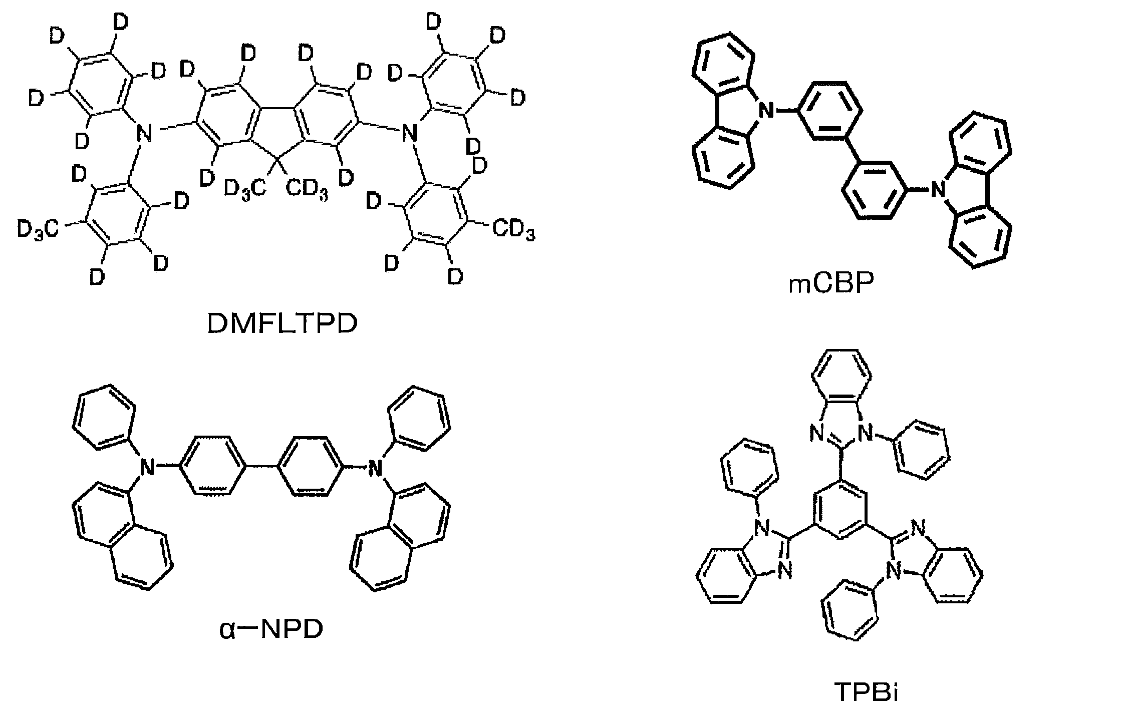
本発明の有機エレクトロルミネッセンス素子は、電流を印加している間と電流の印加を停止した後の両方で発光するため、蓄光照明やパルス駆動方式の照明として好適に用いることができる。このため、本発明は産業上の利用可能性が高い。
The organic electroluminescence device of the present invention emits light both during application of current and after application of current is stopped, and therefore can be suitably used as phosphorescent illumination or pulse drive illumination. For this reason, this invention has high industrial applicability.
1 基板
2 陽極
3 正孔注入層
4 正孔輸送層
5 発光層
6 電子輸送層
7 陰極 DESCRIPTION OFSYMBOLS 1 Substrate 2 Anode 3 Hole injection layer 4 Hole transport layer 5 Light emitting layer 6 Electron transport layer 7 Cathode
2 陽極
3 正孔注入層
4 正孔輸送層
5 発光層
6 電子輸送層
7 陰極 DESCRIPTION OF
Claims (21)
- 一対の電極と、該一対の電極同士の間に発光層を含む少なくとも1層の有機層とを有し、
前記発光層は、π共役性平面分子を含み、
前記一対の電極により、前記発光層に電流を印加した後に電流の印加を停止したとき、電流を印加している間と電流の印加を停止した後の両方で発光することを特徴とする有機エレクトロルミネッセンス素子。 A pair of electrodes, and at least one organic layer including a light emitting layer between the pair of electrodes,
The light emitting layer includes a π-conjugated planar molecule,
When the current application is stopped after applying a current to the light emitting layer, the pair of electrodes emits light both during the application of the current and after the application of the current is stopped. Luminescence element. - 電流を印加している間に蛍光を発光し、電流の印加を停止した後にリン光または遅延蛍光を発光することを特徴とする請求項1に記載の有機エレクトロルミネッセンス素子。 2. The organic electroluminescence device according to claim 1, wherein the organic electroluminescence device emits fluorescence while applying current, and emits phosphorescence or delayed fluorescence after the application of current is stopped.
- 前記π共役性平面分子は、少なくとも1つの芳香環を有することを特徴とする請求項1または2に記載の有機エレクトロルミネッセンス素子。 3. The organic electroluminescence device according to claim 1, wherein the π-conjugated planar molecule has at least one aromatic ring.
- 前記芳香環は、ベンゼン環または2つ以上のベンゼン環が縮合した縮合多環構造の芳香環であることを特徴とする請求項3に有機エレクトロルミネッセンス素子。 The organic electroluminescence device according to claim 3, wherein the aromatic ring is a benzene ring or an aromatic ring having a condensed polycyclic structure in which two or more benzene rings are condensed.
- 前記π共役性平面分子は、水素原子の一部または全部が2H(デューテリウムD)で置換されたD置換体であることを特徴とする請求項1~4のいずれか1項に記載の有機エレクトロルミネッセンス素子。 5. The π-conjugated planar molecule is a D-substituted product in which part or all of hydrogen atoms are substituted with 2 H (deuterium D). Organic electroluminescence device.
- 前記π共役性平面分子は、π共役系を構成する原子団にアミノ基が置換した構造を有する2級アミンまたは3級アミンであることを特徴とする請求項1~5のいずれか1項に記載の有機エレクトロルミネッセンス素子。 6. The π-conjugated planar molecule is a secondary amine or a tertiary amine having a structure in which an amino group is substituted for an atomic group constituting a π-conjugated system, according to any one of claims 1 to 5. The organic electroluminescent element of description.
- 前記アミノ基は、置換もしくは無置換のジアリールアミノ基および置換もしくは無置換のジアルキルアミノ基の少なくとも一方であることを特徴とする請求項6に記載の有機エレクトロルミネッセンス素子。 The organic electroluminescence device according to claim 6, wherein the amino group is at least one of a substituted or unsubstituted diarylamino group and a substituted or unsubstituted dialkylamino group.
- 前記π共役性平面分子は、置換もしくは無置換のフルオレン環を有することを特徴とする請求項1~7のいずれか1項に記載の有機エレクトロルミネッセンス素子。 The organic electroluminescent device according to any one of claims 1 to 7, wherein the π-conjugated planar molecule has a substituted or unsubstituted fluorene ring.
- 前記π共役性平面分子は、下記式で表される化合物、下記式で表される化合物の水素原子の少なくとも1つが置換基で置換された誘導体、または、前記記合物もしくは前記誘導体の水素原子の一部または全部が2H(デューテリウムD)で置換されたD置換体であることを特徴とする請求項1~8のいずれか1項に記載の有機エレクトロルミネッセンス素子。

- 前記発光層は、さらにホスト材料を含むことを特徴とする請求項1~9のいずれか1項に記載の有機エレクトロルミネッセンス素子。 The organic electroluminescence device according to any one of claims 1 to 9, wherein the light emitting layer further contains a host material.
- 前記ホスト材料の最低励起三重項エネルギー準位が、前記π共役性平面分子の最低励起三重項エネルギー準位よりも0.1eV以上高いことを特徴とする請求項10に記載の有機エレクトロルミネッセンス素子。 The organic electroluminescence device according to claim 10, wherein the lowest excited triplet energy level of the host material is 0.1 eV or more higher than the lowest excited triplet energy level of the π-conjugated planar molecule.
- 前記ホスト材料は、少なくとも2つのシクロアルカンが縮合した環状構造または少なくとも2つのシクロアルカンと少なくとも1つのシクロアルケンが縮合した環状構造と、前記環状構造に置換した置換もしくは無置換のカルバゾリル基および置換もしくは無置換のジアリールアミノ基の少なくとも一方を有する化合物であることを特徴とする請求項11に記載の有機エレクトロルミネッセンス素子。 The host material includes a cyclic structure in which at least two cycloalkanes are condensed or a cyclic structure in which at least two cycloalkanes and at least one cycloalkene are condensed, a substituted or unsubstituted carbazolyl group substituted with the cyclic structure, and a substituted or The organic electroluminescence device according to claim 11, wherein the organic electroluminescence device is a compound having at least one of unsubstituted diarylamino groups.
- 前記置換基は、置換もしくは無置換のカルバゾリル基であることを特徴とする請求項12に記載の有機エレクトロルミネッセンス素子。 The organic electroluminescence device according to claim 12, wherein the substituent is a substituted or unsubstituted carbazolyl group.
- 前記ホスト材料は、下記一般式(1)で表される化合物であることを特徴とする請求項10~13のいずれか1項に記載の有機エレクトロルミネッセンス素子。

- 請求項1~14のいずれか1項に記載の有機エレクトロルミネッセンス素子を駆動する駆動方法であって、
前記一対の電極により、前記発光層に電流を印加した後に電流の印加を停止して、電流を印加している間と電流の印加を停止した後の両方で発光を生じさせることを特徴とする有機エレクトロルミネッセンス素子の駆動方法。 A driving method for driving the organic electroluminescence element according to any one of claims 1 to 14,
The pair of electrodes is configured to stop the application of current after applying a current to the light emitting layer, and to emit light both during the application of current and after the application of current is stopped. A driving method of an organic electroluminescence element. - 前記発光層に電流を印加する時間が1μ秒以上であることを特徴とする請求項15に記載の有機エレクトロルミネッセンス素子の駆動方法。 The method for driving an organic electroluminescence element according to claim 15, wherein the time for applying a current to the light emitting layer is 1 µsec or more.
- 前記発光層に、電流を印加するオン期間と電流の印加を停止するオフ期間を交互に繰り返すパルス状のパターンで電流を印加することを特徴とする請求項15または16に記載の有機エレクトロルミネッセンス素子の駆動方法。 17. The organic electroluminescence device according to claim 15, wherein a current is applied to the light emitting layer in a pulse pattern in which an on period in which a current is applied and an off period in which the current application is stopped are alternately repeated. Driving method.
- 前記オン期間が1μ秒~10秒であり、前記オフ期間が1~10分であることを特徴とする請求項17に記載の有機エレクトロルミネッセンス素子の駆動方法。 18. The method of driving an organic electroluminescence element according to claim 17, wherein the on period is 1 μs to 10 seconds and the off period is 1 to 10 minutes.
- 請求項1~14のいずれか1項に記載の有機エレクトロルミネッセンス素子を有することを特徴とする照明装置。 A lighting device comprising the organic electroluminescence element according to any one of claims 1 to 14.
- 電流を印加するオン期間と電流の印加を停止するオフ期間を交互に繰り返すパルス状のパターンで前記発光層に電流を印加するように有機エレクトロルミネッセンス素子を制御する制御手段を有することを特徴とする請求項19に記載の照明装置。 It has a control means for controlling the organic electroluminescence element so as to apply a current to the light emitting layer in a pulsed pattern in which an on period in which current is applied and an off period in which application of current is stopped are alternately repeated. The lighting device according to claim 19.
- 下記一般式(1)で表される化合物。

Priority Applications (1)
| Application Number | Priority Date | Filing Date | Title |
|---|---|---|---|
| JP2016568343A JPWO2016111216A1 (en) | 2015-01-05 | 2015-12-28 | ORGANIC ELECTROLUMINESCENT ELEMENT, ORGANIC ELECTROLUMINESCENT ELEMENT DRIVING METHOD, AND LIGHTING DEVICE |
Applications Claiming Priority (2)
| Application Number | Priority Date | Filing Date | Title |
|---|---|---|---|
| JP2015-000122 | 2015-01-05 | ||
| JP2015000122 | 2015-01-05 |
Publications (1)
| Publication Number | Publication Date |
|---|---|
| WO2016111216A1 true WO2016111216A1 (en) | 2016-07-14 |
Family
ID=56355910
Family Applications (1)
| Application Number | Title | Priority Date | Filing Date |
|---|---|---|---|
| PCT/JP2015/086461 WO2016111216A1 (en) | 2015-01-05 | 2015-12-28 | Organic electroluminescent device, organic-electroluminescent-device driving method, and illumination device |
Country Status (2)
| Country | Link |
|---|---|
| JP (1) | JPWO2016111216A1 (en) |
| WO (1) | WO2016111216A1 (en) |
Cited By (1)
| Publication number | Priority date | Publication date | Assignee | Title |
|---|---|---|---|---|
| WO2016195080A1 (en) * | 2015-06-05 | 2016-12-08 | 国立大学法人九州大学 | Phosphorescent emissive material, method for causing emission of phosphorescence from phosphorescent emitter, method for manufacturing phosphorescent emissive material, organic light emissive element, and gas sensor |
Citations (5)
| Publication number | Priority date | Publication date | Assignee | Title |
|---|---|---|---|---|
| JP2005190797A (en) * | 2003-12-25 | 2005-07-14 | Seiko Epson Corp | Organic el device and electronic apparatus |
| WO2009006990A2 (en) * | 2007-07-06 | 2009-01-15 | Forschungszentrum Karlsruhe Gmbh | Minor splicosome assay system for modulating cell division |
| JP2011118172A (en) * | 2009-12-03 | 2011-06-16 | Kyushu Univ | Low threshold organic inverse-oversaturation absorbing material |
| WO2014034563A1 (en) * | 2012-08-28 | 2014-03-06 | 三星ディスプレイ株式會社 | Composition comprising light-emitting compound exhibiting afterglow |
| JP2015164989A (en) * | 2014-03-03 | 2015-09-17 | 国立大学法人九州大学 | Phosphorescent materials, chemical compound, phosphorescent coating and organic luminous element |
-
2015
- 2015-12-28 JP JP2016568343A patent/JPWO2016111216A1/en active Pending
- 2015-12-28 WO PCT/JP2015/086461 patent/WO2016111216A1/en active Application Filing
Patent Citations (5)
| Publication number | Priority date | Publication date | Assignee | Title |
|---|---|---|---|---|
| JP2005190797A (en) * | 2003-12-25 | 2005-07-14 | Seiko Epson Corp | Organic el device and electronic apparatus |
| WO2009006990A2 (en) * | 2007-07-06 | 2009-01-15 | Forschungszentrum Karlsruhe Gmbh | Minor splicosome assay system for modulating cell division |
| JP2011118172A (en) * | 2009-12-03 | 2011-06-16 | Kyushu Univ | Low threshold organic inverse-oversaturation absorbing material |
| WO2014034563A1 (en) * | 2012-08-28 | 2014-03-06 | 三星ディスプレイ株式會社 | Composition comprising light-emitting compound exhibiting afterglow |
| JP2015164989A (en) * | 2014-03-03 | 2015-09-17 | 国立大学法人九州大学 | Phosphorescent materials, chemical compound, phosphorescent coating and organic luminous element |
Non-Patent Citations (2)
| Title |
|---|
| GERHARD L. CLOSS ET AL.: "Intramolecular Long-Distance Electron Transfer in Organic Molecules", SCIENCE, vol. 240, 22 April 1988 (1988-04-22), pages 440 - 447 * |
| SHUZO HIRATA ET AL.: "Efficient Persistent Room Temperatire Phosphorescence in Organic Amorphous Materials under Ambient Conditions", ADVANCED FUNCTIONAL MATERIALS, vol. 23, 6 February 2013 (2013-02-06), pages 3386 - 3397, XP001585135, DOI: doi:10.1002/adfm.201203706 * |
Cited By (1)
| Publication number | Priority date | Publication date | Assignee | Title |
|---|---|---|---|---|
| WO2016195080A1 (en) * | 2015-06-05 | 2016-12-08 | 国立大学法人九州大学 | Phosphorescent emissive material, method for causing emission of phosphorescence from phosphorescent emitter, method for manufacturing phosphorescent emissive material, organic light emissive element, and gas sensor |
Also Published As
| Publication number | Publication date |
|---|---|
| JPWO2016111216A1 (en) | 2017-11-02 |
Similar Documents
| Publication | Publication Date | Title |
|---|---|---|
| JP6786393B2 (en) | Organic electroluminescent device | |
| JP6600298B2 (en) | Luminescent materials, organic light emitting devices and compounds | |
| JP6526625B2 (en) | Luminescent material, organic light emitting device and compound | |
| JP6668152B2 (en) | Compound, light emitting material and organic light emitting device | |
| JP6466913B2 (en) | Luminescent materials, organic light emitting devices and compounds | |
| WO2020039930A1 (en) | Organic light emitting element, composition and membrane | |
| WO2018159662A1 (en) | Compound, light emitting material and organic light emitting element | |
| JP6383538B2 (en) | Luminescent materials, organic light emitting devices and compounds | |
| WO2015080183A1 (en) | Light-emitting material, organic light-emitting element, and compound | |
| US8512877B2 (en) | Naphthyl carbazole derivatives, KL host material, the organic light emitting device employing the same, the display device and the illumination device employing the same | |
| JP7037543B2 (en) | Organic electroluminescent device | |
| JP2017119663A (en) | Compound, light-emitting material, and organic light-emitting device | |
| JP2014009224A (en) | Light-emitting material, compound, and organic light-emitting element | |
| JP2014009352A (en) | Light-emitting material, compound, and organic light-emitting element | |
| JP2014172852A (en) | Compound, light-emitting material, and organic light-emitting element | |
| KR20110008723A (en) | Novel organic electroluminescent compounds and organic electroluminescent device using the same | |
| JP6647514B2 (en) | Organic light emitting device and light emitting material and compound used therefor | |
| JP2006128624A (en) | Light emitting element | |
| US20210167304A1 (en) | New emitter materials and matrix materials for optoelectronic and electronic components, in particular organic light-emitting diodes (oleds) | |
| WO2017115834A1 (en) | Compound, light-emitting material, and organic light-emitting device | |
| JP2016130231A (en) | Compound, mixture, light-emitting layer, organic light-emitting element, and assist dopant | |
| JP6534250B2 (en) | Host material for delaying phosphor, organic light emitting device and compound | |
| WO2016111216A1 (en) | Organic electroluminescent device, organic-electroluminescent-device driving method, and illumination device | |
| WO2017115835A1 (en) | Compound, light-emitting material, and organic light-emitting device | |
| JP7214142B2 (en) | Singlet fission materials, triplet sensitizers, compounds and thin films |
Legal Events
| Date | Code | Title | Description |
|---|---|---|---|
| 121 | Ep: the epo has been informed by wipo that ep was designated in this application |
Ref document number: 15877088 Country of ref document: EP Kind code of ref document: A1 |
|
| ENP | Entry into the national phase |
Ref document number: 2016568343 Country of ref document: JP Kind code of ref document: A |
|
| NENP | Non-entry into the national phase |
Ref country code: DE |
|
| 122 | Ep: pct application non-entry in european phase |
Ref document number: 15877088 Country of ref document: EP Kind code of ref document: A1 |