WO2016104463A1 - Anisotropic conductive film and connection structure - Google Patents
Anisotropic conductive film and connection structure Download PDFInfo
- Publication number
- WO2016104463A1 WO2016104463A1 PCT/JP2015/085744 JP2015085744W WO2016104463A1 WO 2016104463 A1 WO2016104463 A1 WO 2016104463A1 JP 2015085744 W JP2015085744 W JP 2015085744W WO 2016104463 A1 WO2016104463 A1 WO 2016104463A1
- Authority
- WO
- WIPO (PCT)
- Prior art keywords
- conductive film
- anisotropic conductive
- conductive
- particle arrangement
- arrangement region
- Prior art date
Links
Images

Classifications
-
- H—ELECTRICITY
- H01—ELECTRIC ELEMENTS
- H01R—ELECTRICALLY-CONDUCTIVE CONNECTIONS; STRUCTURAL ASSOCIATIONS OF A PLURALITY OF MUTUALLY-INSULATED ELECTRICAL CONNECTING ELEMENTS; COUPLING DEVICES; CURRENT COLLECTORS
- H01R11/00—Individual connecting elements providing two or more spaced connecting locations for conductive members which are, or may be, thereby interconnected, e.g. end pieces for wires or cables supported by the wire or cable and having means for facilitating electrical connection to some other wire, terminal, or conductive member, blocks of binding posts
- H01R11/01—Individual connecting elements providing two or more spaced connecting locations for conductive members which are, or may be, thereby interconnected, e.g. end pieces for wires or cables supported by the wire or cable and having means for facilitating electrical connection to some other wire, terminal, or conductive member, blocks of binding posts characterised by the form or arrangement of the conductive interconnection between the connecting locations
-
- H—ELECTRICITY
- H01—ELECTRIC ELEMENTS
- H01B—CABLES; CONDUCTORS; INSULATORS; SELECTION OF MATERIALS FOR THEIR CONDUCTIVE, INSULATING OR DIELECTRIC PROPERTIES
- H01B1/00—Conductors or conductive bodies characterised by the conductive materials; Selection of materials as conductors
- H01B1/20—Conductive material dispersed in non-conductive organic material
-
- H—ELECTRICITY
- H01—ELECTRIC ELEMENTS
- H01B—CABLES; CONDUCTORS; INSULATORS; SELECTION OF MATERIALS FOR THEIR CONDUCTIVE, INSULATING OR DIELECTRIC PROPERTIES
- H01B5/00—Non-insulated conductors or conductive bodies characterised by their form
- H01B5/14—Non-insulated conductors or conductive bodies characterised by their form comprising conductive layers or films on insulating-supports
-
- H—ELECTRICITY
- H05—ELECTRIC TECHNIQUES NOT OTHERWISE PROVIDED FOR
- H05K—PRINTED CIRCUITS; CASINGS OR CONSTRUCTIONAL DETAILS OF ELECTRIC APPARATUS; MANUFACTURE OF ASSEMBLAGES OF ELECTRICAL COMPONENTS
- H05K3/00—Apparatus or processes for manufacturing printed circuits
- H05K3/30—Assembling printed circuits with electric components, e.g. with resistor
- H05K3/32—Assembling printed circuits with electric components, e.g. with resistor electrically connecting electric components or wires to printed circuits
-
- H—ELECTRICITY
- H01—ELECTRIC ELEMENTS
- H01R—ELECTRICALLY-CONDUCTIVE CONNECTIONS; STRUCTURAL ASSOCIATIONS OF A PLURALITY OF MUTUALLY-INSULATED ELECTRICAL CONNECTING ELEMENTS; COUPLING DEVICES; CURRENT COLLECTORS
- H01R13/00—Details of coupling devices of the kinds covered by groups H01R12/70 or H01R24/00 - H01R33/00
- H01R13/02—Contact members
- H01R13/22—Contacts for co-operating by abutting
- H01R13/24—Contacts for co-operating by abutting resilient; resiliently-mounted
- H01R13/2407—Contacts for co-operating by abutting resilient; resiliently-mounted characterized by the resilient means
- H01R13/2414—Contacts for co-operating by abutting resilient; resiliently-mounted characterized by the resilient means conductive elastomers
-
- H—ELECTRICITY
- H05—ELECTRIC TECHNIQUES NOT OTHERWISE PROVIDED FOR
- H05K—PRINTED CIRCUITS; CASINGS OR CONSTRUCTIONAL DETAILS OF ELECTRIC APPARATUS; MANUFACTURE OF ASSEMBLAGES OF ELECTRICAL COMPONENTS
- H05K3/00—Apparatus or processes for manufacturing printed circuits
- H05K3/30—Assembling printed circuits with electric components, e.g. with resistor
- H05K3/32—Assembling printed circuits with electric components, e.g. with resistor electrically connecting electric components or wires to printed circuits
- H05K3/321—Assembling printed circuits with electric components, e.g. with resistor electrically connecting electric components or wires to printed circuits by conductive adhesives
- H05K3/323—Assembling printed circuits with electric components, e.g. with resistor electrically connecting electric components or wires to printed circuits by conductive adhesives by applying an anisotropic conductive adhesive layer over an array of pads
Definitions
- the present invention relates to an anisotropic conductive film, a connection method using the anisotropic conductive film, and a connection structure connected by the anisotropic conductive film.
- Anisotropic conductive films are widely used when electronic parts such as IC chips are mounted on a substrate.
- electronic parts such as IC chips are mounted on a substrate.
- insulating adhesives for anisotropic conductive films are used.
- a technique is known in which conductive particles are evenly arranged in a lattice pattern in a layer.
- the conductive particles located on the edges of the terminals are separated by melting of the insulating adhesive.
- the connection resistance varies without being caught between the terminals.
- the first arrangement direction of the conductive particles is the longitudinal direction of the anisotropic conductive film
- the second arrangement direction intersecting the first arrangement direction is the longitudinal direction of the anisotropic conductive film. It has been proposed to incline at an angle of 5 ° or more and 15 ° or less with respect to an orthogonal direction (Patent Document 1).
- the present invention has an object to provide an anisotropic conductive film that can be used for FOG connection and COG connection of fine pitch, and can suppress an increase in manufacturing cost accompanying an increase in the density of conductive particles.
- the present inventor when providing a plurality of arrangement regions having different arrangement mode, arrangement position or density of the conductive particles as the arrangement region of the conductive particles in the anisotropic conductive film, connect with the anisotropic conductive film
- the conductive particle arrangement region according to the object to be formed can be formed, that is, the conductive particle arrangement region can correspond to the outer shape of the terminal arrangement region of the electronic component connected by the anisotropic conductive film (for example, When COG connection is performed with an anisotropic conductive film, conductive particles are arranged in a region corresponding to the peripheral portion of the IC chip where the bump row exists, but conductive particles are arranged in a region corresponding to the central portion where no bump exists.
- the present invention is an anisotropic conductive film comprising an insulating adhesive layer and conductive particles disposed in the insulating adhesive layer, A first conductive particle arrangement region in which a plurality of conductive particles are arranged, and a second conductive particle arrangement region in which the arrangement mode, arrangement position, or density of the conductive particles is different from the first conductive particle arrangement region
- the anisotropic conductive film in which the first conductive particle arrangement region and the second conductive particle arrangement region are periodically formed in the longitudinal direction of the anisotropic conductive film is provided.
- the present invention is an anisotropic conductive film comprising an insulating adhesive layer and conductive particles arranged in the insulating adhesive layer, There is a conductive particle arrangement region (hereinafter also referred to as a conductive particle arrangement region for connection) formed corresponding to the outer shape of the arrangement region of the terminals of the electronic component connected by the anisotropic conductive film, and the conductive particle arrangement region is An anisotropic conductive film that is periodically formed in the longitudinal direction of the anisotropic conductive film is provided.
- the present invention provides a connection structure in which the first electronic component and the second electronic component are anisotropically conductively connected by the anisotropic conductive film described above.
- the anisotropic conductive film of the present invention since the conductive particle arrangement region for connection is formed according to the outer shape of the arrangement region of the terminals, the conductive particles not involved in the connection can be reduced. Manufacturing cost of the conductive film can be suppressed.
- the anisotropic conductive film of the present invention when a conductive particle arrangement region (hereinafter also referred to as alignment conductive particle arrangement region) that serves as an alignment mark is formed, an array of terminals of electronic components to be connected Since the region and the conductive particle arrangement region for connecting the anisotropic conductive film can be aligned, the conductive particles can be surely captured by the terminal and conduction can be ensured.
- alignment conductive particle arrangement region hereinafter also referred to as an alignment mark
- the formation of the conductive particle arrangement region serving as the alignment mark can be formed without requiring an additional step in the conventional manufacturing process of the anisotropic conductive film.
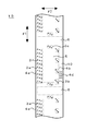
- FIG. 1A is an arrangement view of conductive particles in the anisotropic conductive film 1A.
- FIG. 1B is a plan view of a terminal surface of an IC chip connected by an anisotropic conductive film 1A.
- FIG. 1C is a plan view of a state in which conductive particles are captured by the terminals of the IC chip by thermocompression bonding the anisotropic conductive film 1A to the IC chip.
- FIG. 2 is an arrangement view of conductive particles in the anisotropic conductive film 1B.
- FIG. 3 is an arrangement view of conductive particles in the anisotropic conductive film 1C.
- FIG. 4 is an arrangement view of conductive particles in the anisotropic conductive film 1D.
- FIG. 1A is an arrangement view of conductive particles in the anisotropic conductive film 1A.
- FIG. 1B is a plan view of a terminal surface of an IC chip connected by an anisotropic conductive film 1A.
- FIG. 1C is
- FIG. 5A is an arrangement diagram of conductive particles in a particle arrangement group.
- FIG. 5B is an arrangement diagram of conductive particles in the particle array group.
- FIG. 5C is an arrangement diagram of conductive particles in the particle array group.
- FIG. 5D is a layout diagram of conductive particles in the particle array group.
- FIG. 5E is an arrangement diagram of conductive particles in the particle array group.
- FIG. 6 is an arrangement view of conductive particles in the anisotropic conductive film 1E.
- FIG. 7 is an arrangement view of conductive particles in the anisotropic conductive film 1F.
- FIG. 8A is an arrangement diagram of conductive particles forming a particle array group.
- FIG. 8B is a layout diagram of conductive particles forming a particle array group.
- FIG. 8C is a layout diagram of conductive particles forming a particle array group.
- FIG. 8D is a layout diagram of conductive particles forming a particle array group.
- FIG. 9 is a layout diagram of conductive particles forming a particle array group.
- FIG. 10 is a layout diagram of conductive particles forming a particle array group.
- FIG. 11 is an arrangement view of conductive particles in the anisotropic conductive film 1G.
- FIG. 12 is an arrangement view of conductive particles in the anisotropic conductive film 1H.
- FIG. 13 is an arrangement view of conductive particles in the anisotropic conductive film 1I.
- FIG. 14 is an arrangement view of conductive particles in the anisotropic conductive film 1J.
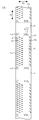
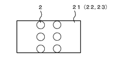
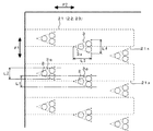
- FIG. 1A is an arrangement view of conductive particles 2 in an anisotropic conductive film 1A of an embodiment of the present invention used for COG connection
- FIG. 1B is a terminal of an IC chip 20 connected by the anisotropic conductive film 1A
- FIG. 1C is a plan view of a state in which conductive particles are captured by the terminals of the IC chip 20 by thermocompression bonding the anisotropic conductive film 1A to the IC chip 20.
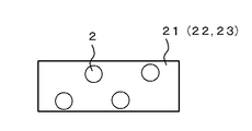
- This anisotropic conductive film 1A has an insulating adhesive layer 10 and conductive particles 2 arranged on the insulating adhesive layer 10. As can be seen from FIG. 1A, FIG. 1B, and FIG. 1C, the conductive particles 2 are arranged corresponding to the arrangement of the terminals of the IC chip 20 in the anisotropic conductive film 1A.
- each particle array group 3a is formed so as to be arranged in the individual output-side bumps 21 of the IC chip 20 when the anisotropic conductive film 1A and the IC chip 20 are overlaid.
- the arrangement of the conductive particles 2 in the particle arrangement group 3a is inclined with respect to the longitudinal direction F1 of the anisotropic conductive film 1A, and the particle trapping property by the output side bumps 21 is improved.
- the outer shape of the conductive particle arrangement region 4a for connection corresponds to the outer shape of the array region 21a of the output-side bump 21. That is, the outer shapes of both are substantially the same, but when the anisotropic conductive film 1A and the IC chip 20 are overlapped, the connecting conductive particle arrangement region 4a covers the arrangement region 21a of the output-side bumps 21.
- the connecting conductive particle arrangement region 4 a is formed to be slightly larger than the arrangement region 21 a of the output-side bump 21. For this reason, both the conductive particle arrangement region 4a for connection and the arrangement region 21a of the output-side bump 21 extend along the longitudinal direction of the anisotropic conductive film 1A.
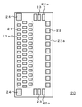
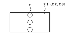
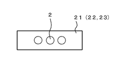
- the particle arrangement group 3b corresponding to the input side bump 22 is arranged in a line along the longitudinal direction F1 of the anisotropic conductive film 1A, thereby forming the conductive particle arrangement region 4b for connection.
- the outer shape of the connecting conductive particle arrangement region 4b corresponds to the outer shape of the arrangement region 22a of the input side bump 22, and the connecting conductive particle arrangement region 4b is formed to cover the arrangement region 22a of the input side bump 22. Yes.
- the particle arrangement group 3c corresponding to the side bumps 23 is arranged in the short direction F2 of the anisotropic conductive film 1A to form the conductive particle arrangement region 4c for connection.
- the outer shape of the connecting conductive particle arrangement region 4 c also corresponds to the outer shape of the arrangement region 23 a of the side bump 23, and the connecting conductive particle arrangement region 4 c is formed to cover the arrangement region 23 a of the side bump 23.
- conductive particle arrangement regions (second conductive particle arrangement regions) 4a, 4b, and 4c having different arrangement modes or arrangement positions of the conductive particles are formed, and these conductive particle arrangement regions are formed.
- the outer shapes of 4a, 4b, and 4c are formed corresponding to the outer shapes of the bump arrangement regions 21a, 22a, and 23a of the IC chip 20, so that the number of conductive particles that are not involved in the connection can be reduced. Thus, the manufacturing cost of the anisotropic conductive film can be suppressed.
- region 4a, 4b, 4c is formed from the particle
- the total connection area of bumps per IC chip is about 5 ⁇ 10 6 ⁇ m 2 , but it can be increased to 1.5 to 3 times. As a result, the IC chip can be further highly integrated.
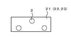
- this anisotropic conductive film 1A the position corresponding to the alignment mark 24 of the IC chip 20 is aligned with the conductive particle arrangement region (first region) by the conductive particles 2 arranged at the four corners and the center of the rectangle.
- Conductive particle arrangement region) 4d is formed.
- the alignment conductive particle arrangement region 4d corresponding to the alignment mark 24 is located at a position different from the connection conductive particle arrangement regions 4a, 4b, and 4c corresponding to the terminal arrangement regions 21a, 22a, and 23a of the IC chip 20.
- the anisotropic conductive film 1A and the IC chip 20 can be used for alignment.
- conductive particles may be further arranged in the alignment conductive particle arrangement region 4d, and the number density of the conductive particles in the region 4d may be higher than that of the connection conductive particle arrangement regions 4a, 4b, and 4c.
- the alignment mark 24 of the IC chip 20 is formed to have a size of several tens ⁇ m to several hundreds ⁇ m, and the alignment between the IC chip and the substrate is performed using a CCD or a laser.
- a mark corresponding to the alignment mark 24 of the IC chip 20 is not formed on the film. This is because in the conventional anisotropic conductive film, the conductive particles are arranged in a monodisperse or lattice form on the entire surface, so the anisotropic conductive film and the substrate or the IC chip are bonded with the accuracy of the bump size. This is because the alignment of the IC chip and the substrate is performed by transmitting a laser beam (used for alignment position detection) through the anisotropic conductive film.
- an alignment mark on the anisotropic conductive film 1A it is conceivable to arrange an insulating adhesive layer having a size corresponding to the alignment mark 24 of the IC chip 20, but the anisotropic conductive film It is difficult due to restrictions on the manufacturing process. Although it is conceivable to directly mark the insulating adhesive layer by printing or the like, the alignment mark is too small and the actual marking processing is difficult.
- the array of conductive particles is used as an alignment mark, it is not necessary to add a new process to the manufacturing process of the anisotropic conductive film, and the manufactured anisotropic conductive film is anisotropically conductive.
- the conductive connection There is no particular limitation when used for the conductive connection, and it is possible to match the positions of the conductive particles in the anisotropic conductive film with the positions of the electrodes on the substrate side corresponding to the bumps of the IC chip. Therefore, in the anisotropic conductive film 1A of the present invention of this example, the conductive particle arrangement region 4d for alignment is formed as an alignment mark.
- the anisotropic conductive film 1A can connect the number of the conductive particles 2 captured by the bumps 21, 22, and 23. Since it is reduced as long as it is ensured, the permeability of the anisotropic conductive film 1A is high. Therefore, it is possible to perform the alignment work through the substrate side. For this reason, the degree of freedom in designing the alignment mark on the IC chip side can be increased, and the alignment mark on the IC chip side can be provided in the vicinity of the bump formation region to improve the alignment accuracy.
- the anisotropic conductive film in 1A 100 [mu] m 2 or more 1 mm 2 or less is preferred in this embodiment for COG.
- the anisotropic conductive film for FOG and FOB it is preferable that the 0.01 mm 2 or more 9 mm 2 or less in order to maintain the detection accuracy.
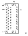
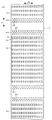
- the anisotropic conductive film 1A includes a conductive particle arrangement region 4a corresponding to the arrangement region 21a of the output side bump 21 of the IC chip 20 and a conductive particle arrangement region 4b corresponding to the arrangement region 22a of the input side bump 22.
- a central region 5 where no conductive particles are arranged is formed between the two.
- the conductive particle arrangement regions 4a, 4b, and 4c corresponding to the bump arrangement regions 21a, 22a, and 23a of the IC chip 20 are periodically and repeatedly formed.
- a buffer region 6 in which no conductive particles are arranged is formed between the conductive particle arrangement regions 4c adjacent in the longitudinal direction F1 of the anisotropic conductive film 1A.
- the anisotropic conductive film 1A is wound and stored in a roll shape, and is used by being pulled out.
- the buffer region 6 is anisotropically conductive wound in a roll shape when the anisotropic conductive film 1A is used.
- the film 1A is pulled out and used for cutting work.
- the length in the longitudinal direction F1 of the anisotropic conductive film 1A in the buffer region 6 is not particularly limited.
- the length of the anisotropic conductive film 1A is 0. 1 mm or more is preferable and 0.2 mm or more is more preferable.
- 10 mm or less is preferable, 3 mm or less is more preferable, and 1 mm or less is even more preferable from the viewpoint of securing a large area that can contribute to connection.
- the conductive particle arrangement regions 4a, 4b, and 4c are formed corresponding to the bump arrangement regions 21a, 22a, and 23a of the IC chip 20, the conductive particles In the arrangement regions 4a, 4b and 4c, the density of the conductive particles 2 can be made appropriate to improve the trapping property of the conductive particles 2 in the bumps, and in the central region 5 and the buffer region 6 corresponding to the regions without the bumps, Since no particles are present, conductive particles not involved in the connection can be reduced. Furthermore, in the conductive particle arrangement regions 4a, 4b, and 4c, particle array groups 3a, 3b, and 3c in which the conductive particles 2 are arranged corresponding to individual bumps are formed. And the occurrence of a short circuit between adjacent bumps can be suppressed.
- the anisotropic conductive film of the present invention can take various forms.
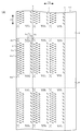
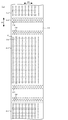
- the conductive particle arrangement for connection corresponding to the arrangement region of the bumps of the IC chip 20 in the longitudinal direction F1 is the same as the anisotropic conductive film 1A.
- the regions 4a, 4b, and 4c are periodically and repeatedly formed, and a plurality of repeating rows of the connecting conductive particle arrangement regions 4a, 4b, and 4c are formed in the short direction F2 of the anisotropic conductive film 1B. Also good.
- This anisotropic conductive film 1 ⁇ / b> B is used after being slit at the position of the slit line 7.
- the particle array group 3b corresponding to the input-side bumps 22 is extended in the short direction F2 of the anisotropic conductive film 1C, and the anisotropic conductive film 1C.
- the slit may be performed by the slit line 7a, or may be performed by the slit line 7b outside by the length of the extended conductive particles. This makes it possible to use the anisotropic conductive film after slitting even if the slit position is shifted in actual slit processing.
- the alignment conductive particle arrangement region 4d used as an alignment mark is formed at a position along the edge in the longitudinal direction F1 of the anisotropic conductive film 1D. Also good.
- the formation arrangement of the alignment conductive particle arrangement region 4d used as the alignment mark can be appropriately changed according to the alignment mark formed on the IC chip.
- the arrangement of conductive particles in the conductive particle arrangement region is not particularly limited.
- the conductive particles 2 form the particle arrangement groups 3a, 3b, and 3c, and the particle arrangement groups 3a, 3b, and 3c are arranged to form the conductive particle arrangement regions 4a, 4b, 4c may be formed, and conductive particles may randomly gather to form a particle group, and the particle group may be arranged in the conductive particle arrangement region, and a single conductive particle may be formed in the conductive particle arrangement region.
- the conductive particles may be arranged in a lattice pattern, or the conductive particles may be randomly arranged within the conductive particle arrangement region.
- the conductive particles are preferably arranged in the conductive particle arrangement region so that the conductive particles are aggregated to such an extent that the outline of the conductive particle arrangement region can be recognized from the viewpoint of accurate alignment.
- the interval between the adjacent conductive particles in the particle arrangement group can be less than 1/4 of the particle diameter of the conductive particles, even if they are in contact with each other. Good.
- the interval between adjacent particle arrangement groups is preferably 0.5 times or more the particle diameter of the conductive particles.
- the particle diameter of the conductive particles is the average diameter of the conductive particles forming the anisotropic conductive film 1A.
- the average diameter of the conductive particles is preferably 1 to 30 ⁇ m, more preferably 1 to 10 ⁇ m, from the viewpoint of preventing short circuit and the stability of the junction between terminals to be connected.
- the number of conductive particles constituting the particle array group can be 2 or more, preferably 3 or more. Further, each particle array group may be in a straight line inclined with respect to the longitudinal direction of the bump, as in the particle array groups 3a, 3b, and 3c of the anisotropic conductive film 1A described above.
- the arrangement of 2 may be a straight line traversing one bump 21 (22, 23) (FIG. 5A), or a straight line traversing one bump 21 (22, 23) (FIG. 5B).
- the bumps 21 (22, 23) may be arranged in a plurality of lines (FIG. 5C), or the conductive particles may be arranged at the vertices of a triangle with respect to one bump 21 (22, 23). (FIG.
- each particle array group is a polygon
- the polygon shape may be a regular triangle, a square, a rectangle, etc., and a polygon shape distorted by one or more vertices protruding, etc. Or a non-symmetric shape may be sufficient. Since bumps are generally rectangular or circular, if there is no similarity or similarity to this, even if irregular particle misalignment occurs when the anisotropic conductive connection is pressed, the trapping property of the conductive particles at the terminal Can be suppressed.
- the conductive particles constituting the particle array group may be in a region corresponding to one bump, and one bump as in the particle array groups 3a and 3b of the anisotropic conductive film 1E shown in FIG.
- the bumps may be formed so as to cross the bumps without being within 21 and 22.
- the dot-filled area indicates the bumps 21 and 22 and the alignment mark 24 of the IC chip connected by the anisotropic conductive film 1E.
- the arrangement direction of the conductive particles in the particle arrangement group may be the longitudinal direction of the anisotropic conductive film 1E as shown in FIG. 6, or the short direction F2 of the anisotropic conductive film 1F (see FIG. 7). That is, it may be the longitudinal direction of each bump 21, 22.
- more than three conductive particles 2 are anisotropically conductive as in the particle array group 3a of the anisotropic conductive film 1F shown in FIG. May be arranged in the short direction F2 of the conductive film (that is, the longitudinal direction of the bumps 21 and 22).
- the arrangement of the conductive particles constituting the particle arrangement group can be appropriately determined according to the shape of the bump itself and the arrangement state of the bump in the IC chip.
- the circumscribed shape of the conductive particles 2 constituting the particle arrangement group 3 is shown. May be a polygon that is a triangle or more, and the particle array group 3 may be arranged in the longitudinal direction of the bump 21.
- the polygonal shape may be a regular polygon or a distorted polygon.
- the direction of each side of the polygon circumscribed by the conductive particles 2 of the particle array group 3 may be a direction intersecting the longitudinal direction F1 or the short direction F2 of the anisotropic conductive film. it can.
- the tolerance for misalignment of the anisotropic conductive film can be increased.
- a conductive particle unit (four conductive particles) 3n composed of a pair of particle array groups spaced so as to straddle the bumps 21 and a particle array group (conducting conductive particles) on the bumps 21 are close to each other.
- (4 particles) 3 m may be arranged.
- the length of the circumscribed bump 21 of the particle array group 3 in the short direction is equal to or less than that of the particle array group 3n longer than the length of the bump short direction.
- the particle array group 3m may be mixed.
- a rectangular particle arrangement group 3m having a short length in the short-bump direction has a circumscribed line Lm in the bump longitudinal direction and a pair of rectangular particle arrangement groups having a long length in the short-bump direction.
- the unit 3n overlaps with the inscribed line Ln in the bump longitudinal direction.
- the length of the particle array group 3 in the short direction of the bump may be larger than the length of the bump 21 in the short direction.
- the conductive particles 2 are easily captured by the bumps 21.
- the projection width L1 of the conductive particles constituting the particle array group 3p on the side extending in the longitudinal direction F1 of the anisotropic conductive film It is preferable to overlap the same projected width L2 of the particle array group 3q adjacent to the particle array group 3p in the transverse direction F2 of the anisotropic conductive film.
- the apex of the triangle is the long side or the short side of the anisotropic conductive film. It is preferable to protrude into.
- the length L3 of the triangle in the short direction F2 of the anisotropic conductive film is equal to the longitudinal direction F1 of the anisotropic conductive film.
- the triangle side 3x intersects the edge 21x of the bump 21 at an acute angle, so that the trapping property of the conductive particles is improved particularly in the case of a fine pitch.
- the arrangement of the conductive particles 2 in the particle arrangement group 3 may be the same or different in each particle arrangement group 3. If different, it can be changed regularly. For example, as shown in FIG. 10, the same number of conductive particles 2 constituting the particle array group 3 and the same circumscribed shape may be used, but particles having different directions of the circumscribed shape may be mixed. As the particle array group 3, particles having different numbers of conductive particles may be regularly and repeatedly arranged.
- the anisotropic conductive film 1G shown in FIG. 11 is obtained by arranging the conductive particles 2 obliquely with respect to the longitudinal direction F1 of the anisotropic conductive film in the particle arrangement group 3a across the plurality of bumps 21. From the viewpoint of improving the particle trapping property of the bumps, the arrangement of the conductive particles in the particle arrangement group is preferably oblique with respect to the longitudinal direction of the anisotropic conductive film 1G.
- the conductive particle arrangement region 4a formed by arranging the particle array group 3a in the longitudinal direction F1 of the anisotropic conductive film is formed on the output side bump of the IC chip. It is formed so as to cover the region, and the end of the outer shape of the conductive particle arrangement region 4a corresponds to the alignment mark 24 of the semiconductor chip. For this reason, in this anisotropic conductive film 1G, an array of conductive particles corresponding to the alignment mark 24 of the IC chip, which is different from the array of conductive particles corresponding to the bumps of the IC chip, is not formed.
- the particle arrangement groups 3a and 3b extending over the plurality of bumps 21 and 22 may have the conductive particles 2 arranged in the longitudinal direction F1 of the anisotropic conductive film 1H.
- Conductive particle arrangement regions 4a and 4b are formed by arranging the particle arrangement groups 3a and 3b in the short direction F2 of the anisotropic conductive film 1H.
- the conductive particles are preferably arranged so that the number of conductive particles captured by one bump is 3 or more, and more preferably 10 or more.
- the length of the anisotropic conductive film in the particle array group in the longitudinal direction is preferably less than 0.8 times the distance between the bumps. Less than twice is more preferable.
- region The 2nd electroconductive particle arrangement
- the conductive particle arrangement region 4e for connection is formed into the anisotropic conductive film. 1I is formed periodically in the longitudinal direction F1.
- the outer shape of the connecting conductive particle arrangement region 4e corresponds to the outer shape of the terminal arrangement region on the substrate.
- alignment conductive particle arrangement regions 4d are periodically formed in the longitudinal direction of the anisotropic conductive film 1I.
- the conductive particle 2 arranges the particle arrangement group 3e in which the anisotropic conductive film 1H is arranged in the longitudinal direction F1 in the short direction F2 of the anisotropic conductive film 1J. Then, the conductive particle arrangement region 4e may be formed, and the conductive particle arrangement region 4e may be periodically formed in the longitudinal direction F1 of the anisotropic conductive film 1H.
- the outer shape of the conductive particle arrangement region 4e also corresponds to the outer shape of the terminal arrangement region on the substrate.
- conductive particle arrangement regions 4d for alignment with alignment marks 24 formed on a glass substrate or a flexible printed wiring board are formed.
- the conductive particles for alignment are formed by forming the end of the conductive particle arrangement region 4e so as to overlap the alignment mark 24.
- the formation of the arrangement region 4d may be omitted, and the end of the conductive particle arrangement region 4e may be used as an alignment mark on the anisotropic conductive film side.
- thermocompression bonding condition at the time of anisotropic conductive connection can be inspected from the indentation, although it is not involved in the connection between the electronic components.
- a relatively large size input / output bump may be provided together with a fine pitch bump array. Therefore, it is also possible to provide a conductive particle arrangement region corresponding to a dummy bump or a relatively large size bump in the anisotropic conductive film, and to replace this with an alignment mark.
- the conductive particles constituting the particle array group can take various arrangements, and when the number of conductive particles captured by each bump is reduced as far as the connection can be secured, the anisotropic at the anisotropic conductive connection In consideration of the flow of the resin constituting the insulating adhesive layer of the conductive film, the bending of the film, the substrate, or the IC chip, it is preferable to appropriately arrange the conductive particles with respect to each bump.
- the density of the conductive particles 2 in the conductive particle arrangement region is not particularly limited and can be appropriately set depending on the target, but is preferably 10 / mm 2 or more, more preferably 1000 / mm 2 or more, and still more preferably. It can be 1000 pieces / mm 2 or more, particularly 2000 pieces / mm 2 or more.
- the upper limit is changed depending on the conditions of the connection object, there is no particular limitation.
- the density of the conductive particles 2 can be 250,000 / mm 2 or less. Usually, 100,000 pieces / mm 2 or less is preferable, and 50,000 pieces / mm 2 or less is more preferable. This particle density is appropriately adjusted according to the particle diameter and arrangement of the conductive particles 2.
- the configuration of the conductive particles 2 itself, the layer configuration of the insulating adhesive layer 10 or the constituent resin can take various forms.
- the conductive particles 2 can be appropriately selected from those used in known anisotropic conductive films.
- examples thereof include metal particles such as nickel, cobalt, silver, copper, gold, and palladium, and metal-coated resin particles. Two or more kinds can be used in combination.
- an insulating resin layer used in a known anisotropic conductive film can be appropriately adopted.
- a photo radical polymerization type resin layer containing an acrylate compound and a photo radical polymerization initiator a heat radical polymerization type resin layer containing an acrylate compound and a heat radical polymerization initiator, a heat containing an epoxy compound and a heat cationic polymerization initiator
- a cationic polymerization type resin layer, a thermal anion polymerization type resin layer containing an epoxy compound and a thermal anion polymerization initiator, or the like can be used.
- Each of these resin layers can be polymerized as necessary.
- the insulating adhesive layer 10 may be formed from a plurality of resin layers.
- the insulating adhesive layer 10 may be added with an insulating filler such as silica fine particles, alumina, and aluminum hydroxide as necessary.
- the blending amount of the insulating filler is preferably 3 to 40 parts by mass with respect to 100 parts by mass of the resin forming the insulating adhesive layer.
- the minimum melt viscosity of the entire insulating adhesive layer is preferably 100 to 10,000 Pa ⁇ s, more preferably 500 to 5000 Pa ⁇ s, and particularly preferably 1000 to 3000 Pa ⁇ s. Within this range, the conductive particles can be precisely arranged in the insulating adhesive layer 10, and it is possible to prevent the resin flow from hindering the trapping property of the conductive particles due to the pressing during anisotropic conductive connection.
- the minimum melt viscosity can be measured using a rheometer (ARES manufactured by TA) under the conditions of a heating rate of 5 ° C./min, a measurement temperature range of 50 to 200 ° C., and a vibration frequency of 1 Hz.
- a mold having a dent corresponding to the arrangement of the conductive particles 2 is produced by a known method such as machining, laser processing, or photolithography. Conductive particles are put into a mold, and an insulating adhesive layer forming composition is filled thereon, cured, and taken out of the mold. From such a mold, the mold may be made of a material having lower rigidity.
- a member having through holes formed in a predetermined arrangement is provided on the insulating adhesive layer-forming composition layer, and from there For example, the conductive particles 2 may be supplied and passed through the through holes.
- connection terminals of first electronic components such as an FPC, a rigid substrate, a ceramic substrate, a plastic substrate, and a glass substrate
- second electronic components such as an IC chip, an IC module, and an FPC
- first electronic components such as an FPC
- second electronic components such as an IC chip, an IC module, and an FPC
- first electronic components such as an FPC
- second electronic components such as an IC chip, an IC module, and an FPC
- the present invention also includes a connection structure of the first electronic component and the second electronic component thus anisotropically connected.
- a mold in which convex portions periodically have an arrangement pattern having a predetermined arrangement density, or the convex portions are randomly arranged at a predetermined arrangement density.
- a mold having a proper arrangement (Comparative Example 1) was prepared, and a known transparent resin pellet was poured into the mold in a molten state, and cooled and hardened to form a resin mold having a lattice-like pattern of recesses. did.
- the resin-shaped recess is filled with conductive particles (Sekisui Chemical Co., Ltd., AUL704, particle size 4 ⁇ m), and the adhesive layer of the above-mentioned insulating resin is placed thereon, and is contained in the insulating resin by ultraviolet curing.
- the curable resin was cured.
- insulating resin was peeled from the type
- the flexible printed circuit board to be FOG connected had a terminal width of 20 ⁇ m, a terminal length of 1 mm, a space between terminals of 20 ⁇ m, and a terminal density corresponding to the bump density of the IC chip of 25 per 1 mm 2 .
- ITO solid glass was used for the glass substrate.
- Example 1 10 conductive particles per electrode terminal (20 ⁇ m ⁇ 1 mm) are arranged so as to be accommodated in the electrode terminals, and the particle array group is arranged so that no conductive particles exist between the electrode terminals. Periodically formed.
- Example 2 14 conductive particles were arranged per electrode terminal (20 ⁇ m ⁇ 1 mm), and a particle array group was periodically formed so that no conductive particles existed between the electrode terminals. In this case, at each electrode terminal, the conductive particles protruded by one conductive particle diameter in the terminal width direction.
- Example 3 a particle array group in which conductive particles are arranged in a tetragonal lattice with an interparticle distance of 4 ⁇ m and arranged in two rows in the short-side direction of the terminal and 40 to 42 rows in the long-side direction of the terminal is arranged on the electrode terminals. Particle array groups were formed periodically. As a result, the total number of conductive particles in the conductive particle arrangement region (including the inter-terminal region) (1 mm 2 ) corresponding to 25 electrode terminals was 2080.
- Example 4 a particle arrangement group of a tetragonal lattice that is substantially the same as that of Example 3, and in each electrode terminal, a particle arrangement group that is arranged in 4 rows in the terminal short direction and 20 to 24 rows in the terminal longitudinal direction. was formed.
- the length of the particle array group in the terminal short direction is longer than the terminal width (the length of the terminal in the short direction).
- the total number of conductive particles in the conductive particle arrangement region (including between terminals) (1 mm 2 ) corresponding to 25 electrode terminals was 2130.
- Comparative Example 1 the conductive particles were randomly arranged so that the number density of the conductive particles was 5000 / mm 2 .
- the anisotropic conductive film of each example and comparative example is sandwiched between an evaluation IC for short-circuit occurrence rate and a glass substrate having a pattern corresponding to the evaluation IC, and heated under the same connection conditions as in (a). Pressurized to obtain a connection object, and the occurrence rate of short circuit of the connection object was determined.
- the short-circuit occurrence rate is calculated by “number of short-circuit occurrences / total number of 7.5 ⁇ m spaces”. A short-circuit occurrence rate of 50 ppm or more is not preferable from the viewpoint of manufacturing a practical connection structure.
- the anisotropic conductive films of Examples 1 to 4 have lower conductive particle number density in the conductive particle arrangement region than Comparative Example 1, but have the same conductive characteristics as Comparative Example 1, and preferable conductive characteristics. It can be seen that the anisotropic conductive film can be manufactured at low cost. In Example 3, 8 ⁇ m, and in Example 4, about 16 ⁇ m, the same results were obtained even when the films were intentionally shifted in the longitudinal direction and bonded together.
- silica filler silica fine particles, Aerosil RY200, Nippon Aerosil Co., Ltd.
- anisotropic conductive films were produced in the same manner, and conduction evaluation was performed. However, both were good.
- the molds (Examples 5 to 9) in which the projections periodically have an array pattern with a predetermined arrangement density or the projections are quadrilateral lattices (grating pitch 8 ⁇ m).
- Mold (Comparative Example 2), and a known transparent resin pellet was poured into the mold in a molten state, cooled and solidified to form a resin mold having a lattice-like pattern of recesses. .
- the resin-shaped recess is filled with conductive particles (Sekisui Chemical Co., Ltd., AUL704, particle size 4 ⁇ m), and the adhesive layer of the above-mentioned insulating resin is placed thereon, and is contained in the insulating resin by ultraviolet curing.
- the curable resin was cured.
- insulating resin was peeled from the type
- the IC chip and the glass substrate for COG connection correspond to their terminal patterns, and the sizes are as shown below.
- IC chip outline 0.7 ⁇ 20mm Thickness 0.2mm Bump specifications Gold plating, height 12 ⁇ m, size 15 ⁇ 100 ⁇ m, space between bumps 13 ⁇ m, number of bumps 1300 (650 on the opposite sides of the IC chip)
- Example 5 to 9 by forming the particle array group with the conductive particle arrangement pattern shown in Table 2 only in the region corresponding to the bump of the IC chip, this particle array group is arranged in the short direction of the bump.
- a conductive particle arrangement region composed of the particle arrangement group shown in Table 2 was formed in a region corresponding to the bump formation region of the IC chip.
- the conductive particles were arranged on the entire bump forming surface of the IC chip in a four-directional lattice arrangement with an interparticle distance of 4 ⁇ m.
- conductive particle arrangement regions were formed in 12 rows (12 rows in total) of 12 sides in a four-sided lattice in accordance with the outer shape of 100 ⁇ m ⁇ 100 ⁇ m as alignment marks.
- a mark (100 ⁇ m ⁇ 100 ⁇ m) corresponding to the alignment mark of the IC chip was provided on the glass substrate.
- the glass substrate and the anisotropic conductive film were manually aligned and temporarily pasted. This temporary sticking was performed at 60 ° C., 2 Mpa, and 1 second.
- the anisotropic conductive film temporarily attached to the glass substrate and the IC chip were aligned and heated and pressed to connect the IC chip.
- a flip chip bonder FC1000 (Toray Engineering Co., Ltd.) was used for the connection of the IC chip.
- the anisotropic conductive films of Examples 5 to 9 have a smaller number of conductive particles in the bump formation region (including the space between the bumps) of the IC chip than Comparative Example 2, but the same as in Comparative Example 2 It can be seen that an anisotropic conductive film having conduction characteristics and favorable conduction characteristics can be manufactured at low cost.
- Examples 10-14 In Examples 5 to 9, 20 parts of silica filler (silica fine particles, Aerosil RY200, Nippon Aerosil Co., Ltd.) was added to 100 parts of insulating resin, and an anisotropic conductive film was produced in the same manner as in Examples 5 to 9. Conductivity evaluation was performed. As a result, all were good.
- silica filler silicon fine particles, Aerosil RY200, Nippon Aerosil Co., Ltd.
- Examples 15-19 anisotropic conductive films were produced in the same manner as in Examples 5 to 9 except that the formation of alignment marks was omitted, and continuity evaluation was performed. As a result, the alignment required more time than in Examples 5 to 9, but the conduction evaluation was good.
- Example 20 In Examples 5 to 9, when the initial conduction resistance was evaluated, the conductive particle arrangement region of the anisotropic conductive film and the bump formation region of the IC chip were slightly shifted and overlapped, and the connection for evaluation was performed by heating and pressing. I got a thing. From the evaluation of the conduction resistance of the connection object for evaluation, the following could be confirmed. That is, in Example 20 (conductive particle arrangement of Example 5), it was found that the conductive particle group can be connected even if the particle size is shifted by one in the width direction of the rectangular bump.
- Example 21 conductive particle arrangement of Example 6
- the connection was possible even when the center of the conductive particle group was shifted from the center of the bump width by 30% (4.5 ⁇ m) of the bump width in the bump width direction.
- Example 22 conductive particle arrangement of Example 7
- the conductive particle group has two conductive particle diameters in the bump width direction. It turned out that it can be connected even if it is misaligned.
- Example 23 (conducting particle arrangement of Example 8), it was found that the connection was possible even when the center of the conductive particle group arranged in a rectangle was shifted by three conductive particle diameters in the bump width direction with respect to the center of the bump width. .
- Example 24 (conductive particle arrangement of Example 9), it was found that the connection was possible even when the center of the conductive particle group arranged in a rectangle was shifted by three conductive particle diameters in the bump width direction with respect to the center of the bump width. . In addition, the state of the electroconductive particle pressed rather than Example 8 was favorable.
- Example 15 the conductive particles corresponding to one bump were arranged in the particle array group 3 shown in FIGS. 8A to 8D and FIG. 10, and the conduction evaluation was performed in the same manner as in Example 15.
- the size of the bump is 15 ⁇ m ⁇ 100 ⁇ m as in Example 15
- the space between the bumps is 13 ⁇ m
- the number of trapped conductive particles per bump is 12 in the mode of FIG. 8A and the mode of FIG. 8B.
- 16 12 in the embodiment of FIG. 8C, 15 in the embodiment of FIG. 8D, and 16 in the embodiment of FIG. 10. In any of these cases, a good connection state was obtained.
- Anisotropic conductive film 2 Conductive particles 3, 3a, 3b, 3c, 3e, 3m, 3p, 3q Particle array group 4a, 4b, 4c 4e Conductive particle arrangement region for connection 4d Conductive particle arrangement region for alignment 5 Central region where no conductive particles are arranged 6 Buffer region where no conductive particles are arranged 7, 7a, 7b Slit line 10 Insulating adhesive layer 20 IC chip 21 Output side bump 21a Output side bump arrangement area 22 Input side bump 22a Input side bump arrangement area 23 Side bump 23a Side bump arrangement area 24 Alignment mark 30 Substrate electrode terminal 31 Substrate alignment mark F1 Anisotropic conductivity Direction of conductive film F2 Short direction of anisotropic conductive film
Abstract
Description
複数の導電粒子が配置されている第1の導電粒子配置領域、及び第1の導電粒子配置領域に対して導電粒子の配列態様、配列位置又は密度が異なる第2の導電粒子配置領域を有し、第1の導電粒子配置領域及び第2の導電粒子配列領域が異方導電性フィルムの長手方向に周期的に形成されている異方導電性フィルムを提供する。 That is, the present invention is an anisotropic conductive film comprising an insulating adhesive layer and conductive particles disposed in the insulating adhesive layer,
A first conductive particle arrangement region in which a plurality of conductive particles are arranged, and a second conductive particle arrangement region in which the arrangement mode, arrangement position, or density of the conductive particles is different from the first conductive particle arrangement region The anisotropic conductive film in which the first conductive particle arrangement region and the second conductive particle arrangement region are periodically formed in the longitudinal direction of the anisotropic conductive film is provided.
異方導電性フィルムで接続する電子部品の端子の配列領域の外形に対応して形成された導電粒子配置領域(以下、接続用導電粒子配置領域ともいう)を有し、該導電粒子配置領域が、異方導電性フィルムの長手方向に周期的に形成されている異方導電性フィルムを提供する。 Further, the present invention is an anisotropic conductive film comprising an insulating adhesive layer and conductive particles arranged in the insulating adhesive layer,
There is a conductive particle arrangement region (hereinafter also referred to as a conductive particle arrangement region for connection) formed corresponding to the outer shape of the arrangement region of the terminals of the electronic component connected by the anisotropic conductive film, and the conductive particle arrangement region is An anisotropic conductive film that is periodically formed in the longitudinal direction of the anisotropic conductive film is provided.
実施例1~4、比較例1
(1)FOG接続用の異方導電性フィルムの製造
フェノキシ樹脂(熱可塑性樹脂)(新日鐵住金(株)、YP-50)60部、エポキシ樹脂(熱硬化性樹脂)(三菱化学(株)、jER828)40部、カチオン系硬化剤(三新化学工業(株)、SI-60L)2部を含む絶縁性樹脂の混合溶液を調製し、それを、フィルム厚さ50μmのPETフィルム上に塗布し、80℃のオーブンにて5分間乾燥させ、PETフィルム上に厚み20μmの粘着層を形成した。 Hereinafter, based on an Example, this invention is demonstrated concretely.
Examples 1 to 4 and Comparative Example 1
(1) Manufacture of anisotropic conductive film for FOG connection 60 parts of phenoxy resin (thermoplastic resin) (Nippon Steel & Sumitomo Metal Corporation, YP-50), epoxy resin (thermosetting resin) (Mitsubishi Chemical Corporation) ), JER828) 40 parts, and a cationic curing agent (Sanshin Chemical Industry Co., Ltd., SI-60L) 2 parts of a mixed solution of an insulating resin was prepared, and this was placed on a PET film having a film thickness of 50 μm. It was applied and dried in an oven at 80 ° C. for 5 minutes to form an adhesive layer having a thickness of 20 μm on the PET film.
ガラス基板はITOベタガラスを使用した。 Here, the flexible printed circuit board to be FOG connected had a terminal width of 20 μm, a terminal length of 1 mm, a space between terminals of 20 μm, and a terminal density corresponding to the bump density of the IC chip of 25 per 1 mm 2 .
ITO solid glass was used for the glass substrate.
実施例1~4及び比較例1の異方導電性フィルムの(a)初期導通抵抗、(b)導通信頼性、(c)ショート発生率を、それぞれ次のように評価した。結果を表1に示す。 (2) Conductivity evaluation The anisotropic conductive films of Examples 1 to 4 and Comparative Example 1 were evaluated for (a) initial conduction resistance, (b) conduction reliability, and (c) short-circuit occurrence rate as follows. . The results are shown in Table 1.
実施例1~4及び比較例1の異方導電性フィルムを、上述のフレキシブルプリント基板とガラス基板との間に挟み、加熱加圧(180℃、5MPa、5秒)して各評価用接続物を得、その評価用接続物の導通抵抗を測定した。 (a) Initial conduction resistance The anisotropic conductive films of Examples 1 to 4 and Comparative Example 1 were sandwiched between the above-mentioned flexible printed circuit board and glass substrate, and heated and pressurized (180 ° C., 5 MPa, 5 seconds). Then, each connection object for evaluation was obtained, and the conduction resistance of the connection object for evaluation was measured.
(a)初期導通抵抗の評価用接続物を温度85℃、湿度85%RHの恒温槽に500時間おき、その導通抵抗を、(a)と同様に測定した。なお、この導通抵抗が5Ω以上であると、接続した電子部品の実用的な導通安定性の点から好ましくない。 (b) Conduction reliability (a) Connection for evaluation of initial conduction resistance was placed in a thermostatic chamber at 85 ° C. and humidity 85% RH for 500 hours, and the conduction resistance was measured in the same manner as (a). In addition, it is unpreferable from the point of practical conduction stability of the connected electronic component that this conduction resistance is 5 ohms or more.
ショート発生率の評価用ICとして次のIC(7.5μmスペースの櫛歯TEG(test element group))を用意した。 (c) Short-circuit occurrence rate The following IC (a comb element TEG (test element group with 7.5 μm space)) was prepared as an IC for evaluating the short-circuit occurrence rate.
厚み 0.5mm
バンプ仕様 金メッキ、高さ15μm、サイズ25×140μm、バンプ間距離7.5μm Outer diameter 1.5 × 13mm
Thickness 0.5mm
Bump specifications Gold plating, height 15μm, size 25 × 140μm, distance between bumps 7.5μm

(1)COG接続用の異方導電性フィルムの製造
実施例1と同様にして、フェノキシ樹脂(熱可塑性樹脂)(新日鐵住金(株)、YP-50)60部、エポキシ樹脂(熱硬化性樹脂)(三菱化学(株)、jER828)40部、カチオン系硬化剤(三新化学工業(株)、SI-60L)2部を用いてPETフィルム上に厚み20μmの粘着層を形成した。 Examples 5 to 9, Comparative Example 2
(1) Production of anisotropic conductive film for COG connection In the same manner as in Example 1, 60 parts of phenoxy resin (thermoplastic resin) (Nippon Steel & Sumitomo Metal Corporation, YP-50), epoxy resin (thermosetting) (Adhesive resin) (Mitsubishi Chemical Corporation, jER828) 40 parts and a cationic curing agent (Sanshin Chemical Industry Co., Ltd., SI-60L) 2 parts were used to form a 20 μm thick adhesive layer on the PET film.
外形 0.7×20mm
厚み 0.2mm
バンプ仕様 金メッキ、高さ12μm、サイズ15×100μm、バンプ間スペース13μm、バンプ個数 1300個(ICチップの長手の対向する辺にそれぞれ650個) IC chip outline 0.7 × 20mm
Thickness 0.2mm
Bump specifications Gold plating, height 12 μm, size 15 × 100 μm, space between bumps 13 μm, number of bumps 1300 (650 on the opposite sides of the IC chip)
ガラス材質 コーニング社製
外径 30×50mm
厚み 0.5mm
電極 ITO配線 Glass substrate Glass material Corning Co., Ltd. Outer diameter 30 × 50mm
Thickness 0.5mm
Electrode ITO wiring
実施例5~9及び比較例2の異方導電性フィルムの(a)初期導通抵抗、(b)導通信頼性、(c)ショート発生率を、それぞれ次のように評価した。結果を表2に示す。 (2) Conductivity evaluation The anisotropic conductive films of Examples 5 to 9 and Comparative Example 2 were evaluated for (a) initial conduction resistance, (b) conduction reliability, and (c) short-circuit occurrence rate as follows. . The results are shown in Table 2.
実施例5~9及び比較例2の異方導電性フィルムを、上述のICチップとそれに対応するガラス基板との間に挟み、加熱加圧(180℃、80MPa、5秒)して各評価用接続物を得、その評価用接続物の導通抵抗を測定した。 (a) Initial conduction resistance The anisotropic conductive films of Examples 5 to 9 and Comparative Example 2 were sandwiched between the above-mentioned IC chip and the corresponding glass substrate, and heated and pressurized (180 ° C., 80 MPa, 5 seconds) ) To obtain each evaluation connection, and the conduction resistance of the evaluation connection was measured.
実施例1と同様にしてショート導通信頼性を測定した。この導通抵抗が5Ω以上であると、接続した電子部品の実用的な導通安定性の点から好ましくない。 (b) Conduction reliability Short circuit conduction reliability was measured in the same manner as in Example 1. When the conduction resistance is 5Ω or more, it is not preferable from the viewpoint of practical conduction stability of the connected electronic component.
実施例1と同様にしてショート発生率を評価した。ショート発生率が50ppm以上であると実用上の接続構造体を製造する点から好ましくない。 (c) Short-circuit occurrence rate The short-circuit occurrence rate was evaluated in the same manner as in Example 1. A short-circuit occurrence rate of 50 ppm or more is not preferable from the viewpoint of manufacturing a practical connection structure.

実施例5~9において、絶縁性樹脂100部にシリカフィラー(シリカ微粒子、アエロジルRY200、日本アエロジル(株))20部を追加し、実施例5~9と同様に異方導電性フィルムを製造し、導通評価を行った。その結果、いずれも良好であった。 Examples 10-14
In Examples 5 to 9, 20 parts of silica filler (silica fine particles, Aerosil RY200, Nippon Aerosil Co., Ltd.) was added to 100 parts of insulating resin, and an anisotropic conductive film was produced in the same manner as in Examples 5 to 9. Conductivity evaluation was performed. As a result, all were good.
実施例5~9において、アライメントマークの形成を省略する以外は、実施例5~9と同様に異方導電性フィルムを製造し、導通評価を行った。その結果、実施例5~9に比してアライメントに時間を要したが、導通評価は良好であった。 Examples 15-19
In Examples 5 to 9, anisotropic conductive films were produced in the same manner as in Examples 5 to 9 except that the formation of alignment marks was omitted, and continuity evaluation was performed. As a result, the alignment required more time than in Examples 5 to 9, but the conduction evaluation was good.
実施例5~9において、初期導通抵抗の評価時に、異方導電性フィルムの導電粒子配置領域とICチップのバンプ形成領域とが僅かにずれて重ね合わさったものを加熱加圧することにより評価用接続物を得た。この評価用接続物の導通抵抗の評価から次のことを確認できた。即ち、実施例20(実施例5の導電粒子配置)において、導電粒子群が矩形のバンプの幅方向に粒子径1個分ずれても接続できることがわかった。 Examples 20-24
In Examples 5 to 9, when the initial conduction resistance was evaluated, the conductive particle arrangement region of the anisotropic conductive film and the bump formation region of the IC chip were slightly shifted and overlapped, and the connection for evaluation was performed by heating and pressing. I got a thing. From the evaluation of the conduction resistance of the connection object for evaluation, the following could be confirmed. That is, in Example 20 (conductive particle arrangement of Example 5), it was found that the conductive particle group can be connected even if the particle size is shifted by one in the width direction of the rectangular bump.
実施例15において、1つのバンプに対応する導電粒子の配置を図8A~図8D及び図10に示した粒子配列群3の配列とし、実施例15と同様に導通評価を行った。この場合、バンプの大きさは実施例15と同様に15μm×100μm、バンプ間スペースは13μmであり、バンプ1個あたりの導電粒子の捕捉数は、図8Aの態様では12個、図8Bの態様では16個、図8Cの態様では12個、図8Dの態様では15個、図10の態様で16個である。これらのいずれにおいても良好な接続状態を得られた。 Examples 25-29
In Example 15, the conductive particles corresponding to one bump were arranged in the
2 導電粒子
3、3a、3b、3c、3e、3m、3p、3q 粒子配列群
4a、4b、4c、4e 接続用導電粒子配置領域
4d 位置合わせ用導電粒子配置領域
5 導電粒子が配置されていない中央部領域
6 導電粒子が配置されていないバッファー領域
7、7a、7b スリット線
10 絶縁接着剤層
20 ICチップ
21 出力側バンプ
21a 出力側バンプの配列領域
22 入力側バンプ
22a 入力側バンプの配列領域
23 サイドバンプ
23a サイドバンプの配列領域
24 アライメントマーク
30 基板の電極端子
31 基板のアライメントマーク
F1 異方導電性フィルムの長手方向
F2 異方導電性フィルムの短手方向 1A, 1B, 1C, 1D, 1E, 1F, 1G, 1H, 1I, 1J Anisotropic
Claims (14)
- 絶縁接着剤層と、該絶縁接着剤層に配置された導電粒子を含む異方導電性フィルムであって、
異方導電性フィルムで接続する電子部品の端子の配列領域の外形に対応して形成された導電粒子配置領域(以下、接続用導電粒子配置領域ともいう)を有し、該導電粒子配置領域が、異方導電性フィルムの長手方向に周期的に形成されている異方導電性フィルム。 An anisotropic conductive film comprising an insulating adhesive layer and conductive particles arranged in the insulating adhesive layer,
There is a conductive particle arrangement region (hereinafter also referred to as a conductive particle arrangement region for connection) formed corresponding to the outer shape of the arrangement region of the terminals of the electronic component connected by the anisotropic conductive film, and the conductive particle arrangement region is An anisotropic conductive film formed periodically in the longitudinal direction of the anisotropic conductive film. - 隣り合う接続用導電粒子配置領域の間に、導電粒子が配置されていないバッファー領域を有する請求項1記載の異方導電性フィルム。 The anisotropic conductive film according to claim 1, further comprising a buffer region in which no conductive particles are arranged between adjacent conductive particle arrangement regions for connection.
- 異方導電性接続する端子と異方導電性フィルムとの位置合わせのためのアライメントマークとなる導電粒子配置領域(以下、位置合わせ用導電粒子配置領域ともいう)を有する請求項1又は2記載の異方導電性フィルム。 The conductive particle arrangement region (hereinafter also referred to as alignment conductive particle arrangement region) serving as an alignment mark for alignment between the anisotropically conductive terminal and the anisotropic conductive film is provided. Anisotropic conductive film.
- 位置合わせ用導電粒子配置領域が接続用導電粒子配置領域と別個に形成されている請求項1~3のいずれかに記載の異方導電性フィルム。 4. The anisotropic conductive film according to claim 1, wherein the alignment conductive particle arrangement region is formed separately from the connection conductive particle arrangement region.
- 位置合わせ用導電粒子配置領域が、接続用導電粒子配置領域と重複して形成されている請求項1~3のいずれかに記載の異方導電性フィルム。 4. The anisotropic conductive film according to claim 1, wherein the conductive particle arrangement region for alignment overlaps with the conductive particle arrangement region for connection.
- 接続用導電粒子配置領域に、複数の導電粒子で形成された粒子配列群が配列している請求項1~5のいずれかに記載の異方導電性フィルム。 6. The anisotropic conductive film according to claim 1, wherein a particle arrangement group formed of a plurality of conductive particles is arranged in the conductive particle arrangement region for connection.
- 接続用導電粒子配置領域において、異方導電性フィルムで接続する電子部品の一つのバンプあたり3個以上の導電粒子が配置されている請求項1~6のいずれかに記載の異方導電性フィルム。 The anisotropic conductive film according to any one of claims 1 to 6, wherein in the conductive particle arrangement region for connection, three or more conductive particles are arranged per bump of an electronic component connected by the anisotropic conductive film. .
- 複数の接続用導電粒子配置領域がそれぞれ異方導電性フィルムの長手方向に周期的に形成されている請求項1~7のいずれかに記載の異方導電性フィルム。 The anisotropic conductive film according to any one of claims 1 to 7, wherein a plurality of conductive particle arrangement regions for connection are each periodically formed in the longitudinal direction of the anisotropic conductive film.
- 異方導電性フィルムの長手方向に沿って接続用導電粒子配置領域が並列して形成されている請求項1~8のいずれかに記載の異方導電性フィルム。 The anisotropic conductive film according to any one of claims 1 to 8, wherein conductive particle arrangement regions for connection are formed in parallel along the longitudinal direction of the anisotropic conductive film.
- 絶縁接着剤層と、該絶縁接着剤層に配置された導電粒子を含む異方導電性フィルムであって、
複数の導電粒子が配置されている第1の導電粒子配置領域、及び第1の導電粒子配置領域に対して導電粒子の配列態様、配列位置又は密度が異なる第2の導電粒子配置領域を有し、第1の導電粒子配置領域及び第2の導電粒子配列領域が異方導電性フィルムの長手方向に周期的に形成されている異方導電性フィルム。 An anisotropic conductive film comprising an insulating adhesive layer and conductive particles arranged in the insulating adhesive layer,
A first conductive particle arrangement region in which a plurality of conductive particles are arranged, and a second conductive particle arrangement region in which the arrangement mode, arrangement position, or density of the conductive particles is different from the first conductive particle arrangement region The anisotropic conductive film in which the first conductive particle arrangement region and the second conductive particle arrangement region are periodically formed in the longitudinal direction of the anisotropic conductive film. - 異方導電性フィルムの長手方向に隣り合う第2の導電粒子配置領域の間に、導電粒子が配置されていないバッファー領域を有する請求項10記載の異方導電性フィルム。 The anisotropic conductive film according to claim 10, further comprising a buffer region in which no conductive particles are arranged between second conductive particle arrangement regions adjacent to each other in the longitudinal direction of the anisotropic conductive film.
- 第1の導電粒子配置領域が、位置合わせ用導電粒子配置領域である請求項10又は11記載の異方導電性フィルム。 The anisotropic conductive film according to claim 10 or 11, wherein the first conductive particle arrangement region is an alignment conductive particle arrangement region.
- 第2の導電粒子配置領域が、接続用導電粒子配置領域である請求項10~12のいずれかに記載の異方導電性フィルム。 The anisotropic conductive film according to any one of claims 10 to 12, wherein the second conductive particle arrangement region is a connection conductive particle arrangement region.
- 請求項1~13のいずれかに記載の異方導電性フィルムで第1電子部品と第2電子部品が異方導電性接続されている接続構造体。 A connection structure in which the first electronic component and the second electronic component are anisotropically conductively connected with the anisotropic conductive film according to any one of claims 1 to 13.
Priority Applications (3)
| Application Number | Priority Date | Filing Date | Title |
|---|---|---|---|
| US15/538,525 US9991614B2 (en) | 2014-12-22 | 2015-12-22 | Anisotropic electrically conductive film and connection structure |
| CN201580066924.4A CN107004974B (en) | 2014-12-22 | 2015-12-22 | Anisotropic conductive film and connection structure |
| KR1020177015109A KR101929697B1 (en) | 2014-12-22 | 2015-12-22 | Anisotropic conductive film and connection structure |
Applications Claiming Priority (2)
| Application Number | Priority Date | Filing Date | Title |
|---|---|---|---|
| JP2014259509 | 2014-12-22 | ||
| JP2014-259509 | 2014-12-22 |
Publications (1)
| Publication Number | Publication Date |
|---|---|
| WO2016104463A1 true WO2016104463A1 (en) | 2016-06-30 |
Family
ID=56150481
Family Applications (1)
| Application Number | Title | Priority Date | Filing Date |
|---|---|---|---|
| PCT/JP2015/085744 WO2016104463A1 (en) | 2014-12-22 | 2015-12-22 | Anisotropic conductive film and connection structure |
Country Status (6)
| Country | Link |
|---|---|
| US (1) | US9991614B2 (en) |
| JP (3) | JP6759578B2 (en) |
| KR (1) | KR101929697B1 (en) |
| CN (1) | CN107004974B (en) |
| TW (1) | TWI686014B (en) |
| WO (1) | WO2016104463A1 (en) |
Cited By (3)
| Publication number | Priority date | Publication date | Assignee | Title |
|---|---|---|---|---|
| CN107452438A (en) * | 2017-07-27 | 2017-12-08 | 京东方科技集团股份有限公司 | A kind of anisotropy conductiving glue band and tape roll, binding structure and display device |
| WO2018101108A1 (en) * | 2016-12-01 | 2018-06-07 | デクセリアルズ株式会社 | Anisotropic conductive film |
| TWI763750B (en) * | 2016-12-01 | 2022-05-11 | 日商迪睿合股份有限公司 | Anisotropic conductive film |
Families Citing this family (9)
| Publication number | Priority date | Publication date | Assignee | Title |
|---|---|---|---|---|
| KR102535557B1 (en) * | 2016-03-07 | 2023-05-24 | 삼성디스플레이 주식회사 | Display apparatus and electronic device |
| US20210249793A1 (en) * | 2018-06-06 | 2021-08-12 | Dexerials Corporation | Connection body, method for manufacturing connection body, and connection method |
| JP7321792B2 (en) * | 2019-06-26 | 2023-08-07 | 株式会社ジャパンディスプレイ | Anisotropic conductive film and display device |
| KR20210018700A (en) | 2019-08-09 | 2021-02-18 | 삼성디스플레이 주식회사 | Adhesive member and display device comprising the adhesive member |
| CN111303795A (en) * | 2020-02-14 | 2020-06-19 | 维沃移动通信有限公司 | Anisotropic conductive adhesive film, preparation method thereof and display device |
| KR20210122359A (en) | 2020-03-30 | 2021-10-12 | 삼성디스플레이 주식회사 | Display device and manufacturing method for the same |
| KR20210138332A (en) * | 2020-05-12 | 2021-11-19 | 안성룡 | A method for boning the conductive thing to the lid |
| KR20230109182A (en) * | 2021-03-26 | 2023-07-19 | 데쿠세리아루즈 가부시키가이샤 | filler array film |
| WO2022202987A1 (en) * | 2021-03-26 | 2022-09-29 | デクセリアルズ株式会社 | Filler disposition film |
Citations (3)
| Publication number | Priority date | Publication date | Assignee | Title |
|---|---|---|---|---|
| JPH09320345A (en) * | 1996-05-31 | 1997-12-12 | Whitaker Corp:The | Anisotropic conductive film |
| WO2008029580A1 (en) * | 2006-08-29 | 2008-03-13 | Hitachi Chemical Company, Ltd. | Anisotropic conductive tape and method of manufacturing it, connected structure and method of connecting circuit member by use of the tape |
| WO2008143358A1 (en) * | 2007-05-24 | 2008-11-27 | Sony Chemical & Information Device Corporation | Electric device, connecting method and adhesive film |
Family Cites Families (17)
| Publication number | Priority date | Publication date | Assignee | Title |
|---|---|---|---|---|
| JPH0660979B2 (en) * | 1985-08-30 | 1994-08-10 | 松下電器産業株式会社 | Electrical connection method |
| JPH10209210A (en) * | 1997-01-20 | 1998-08-07 | Sharp Corp | Semiconductor device, its manufacture, and its inspection method |
| JP3506003B2 (en) * | 1998-05-19 | 2004-03-15 | ソニーケミカル株式会社 | Anisotropic conductive adhesive |
| JP2002094222A (en) * | 2000-09-19 | 2002-03-29 | Matsushita Electric Ind Co Ltd | Sheet for bonding electronic component, method for mounting electronic component, and equipment for mounting the same |
| JP2004071857A (en) * | 2002-08-07 | 2004-03-04 | Sharp Corp | Structure of substrate connection part, electronic component having the structure and liquid crystal display device |
| JP3994335B2 (en) * | 2002-10-04 | 2007-10-17 | 日立化成工業株式会社 | Manufacturing method of connecting member |
| JP4887700B2 (en) | 2005-09-09 | 2012-02-29 | 住友ベークライト株式会社 | Anisotropic conductive film and electronic / electrical equipment |
| JP2007115560A (en) | 2005-10-21 | 2007-05-10 | Sumitomo Bakelite Co Ltd | Anisotropic conductive film and its manufacturing method |
| KR100803433B1 (en) * | 2006-01-23 | 2008-02-13 | 엘에스전선 주식회사 | Anisotropic conductive film with highly reliable bonding and circuit connecting structure using anisotropic conductive film |
| CN101512840A (en) * | 2006-08-29 | 2009-08-19 | 日立化成工业株式会社 | Anisotropic conductive tape and method of manufacturing it, connected structure and method of connecting circuit member by use of the tape |
| CN101556838B (en) * | 2008-04-09 | 2011-06-01 | 北京京东方光电科技有限公司 | Anisotropic conductive film |
| JP5543267B2 (en) * | 2010-05-07 | 2014-07-09 | デクセリアルズ株式会社 | Anisotropic conductive film and manufacturing method thereof, and mounting body and manufacturing method thereof |
| JP5690648B2 (en) * | 2011-04-28 | 2015-03-25 | デクセリアルズ株式会社 | Anisotropic conductive film, connection method and connection structure |
| JP5293843B2 (en) * | 2012-01-24 | 2013-09-18 | デクセリアルズ株式会社 | Transparent conductive element, input device, electronic device and transparent conductive element manufacturing master |
| TWI613684B (en) | 2012-08-01 | 2018-02-01 | Dexerials Corp | Method for producing anisotropic conductive film, anisotropic conductive film, and connection structure |
| KR20210146455A (en) * | 2012-08-01 | 2021-12-03 | 데쿠세리아루즈 가부시키가이샤 | Method for manufacturing anisotropically conductive film, anisotropically conductive film, and connective structure |
| JP6476747B2 (en) * | 2014-10-28 | 2019-03-06 | デクセリアルズ株式会社 | Anisotropic conductive film and connection structure |
-
2015
- 2015-12-21 JP JP2015249132A patent/JP6759578B2/en active Active
- 2015-12-22 US US15/538,525 patent/US9991614B2/en active Active
- 2015-12-22 WO PCT/JP2015/085744 patent/WO2016104463A1/en active Application Filing
- 2015-12-22 CN CN201580066924.4A patent/CN107004974B/en active Active
- 2015-12-22 TW TW104143326A patent/TWI686014B/en active
- 2015-12-22 KR KR1020177015109A patent/KR101929697B1/en active IP Right Grant
-
2020
- 2020-06-30 JP JP2020112766A patent/JP7176550B2/en active Active
-
2022
- 2022-11-10 JP JP2022180551A patent/JP2023001341A/en active Pending
Patent Citations (3)
| Publication number | Priority date | Publication date | Assignee | Title |
|---|---|---|---|---|
| JPH09320345A (en) * | 1996-05-31 | 1997-12-12 | Whitaker Corp:The | Anisotropic conductive film |
| WO2008029580A1 (en) * | 2006-08-29 | 2008-03-13 | Hitachi Chemical Company, Ltd. | Anisotropic conductive tape and method of manufacturing it, connected structure and method of connecting circuit member by use of the tape |
| WO2008143358A1 (en) * | 2007-05-24 | 2008-11-27 | Sony Chemical & Information Device Corporation | Electric device, connecting method and adhesive film |
Cited By (8)
| Publication number | Priority date | Publication date | Assignee | Title |
|---|---|---|---|---|
| WO2018101108A1 (en) * | 2016-12-01 | 2018-06-07 | デクセリアルズ株式会社 | Anisotropic conductive film |
| CN109964371A (en) * | 2016-12-01 | 2019-07-02 | 迪睿合株式会社 | Anisotropic conductive film |
| CN109964371B (en) * | 2016-12-01 | 2021-03-12 | 迪睿合株式会社 | Anisotropic conductive film |
| US10957462B2 (en) | 2016-12-01 | 2021-03-23 | Dexerials Corporation | Anisotropic conductive film |
| TWI763750B (en) * | 2016-12-01 | 2022-05-11 | 日商迪睿合股份有限公司 | Anisotropic conductive film |
| CN107452438A (en) * | 2017-07-27 | 2017-12-08 | 京东方科技集团股份有限公司 | A kind of anisotropy conductiving glue band and tape roll, binding structure and display device |
| CN107452438B (en) * | 2017-07-27 | 2019-10-11 | 京东方科技集团股份有限公司 | A kind of anisotropy conductiving glue band and tape roll, binding structure and display device |
| US10510708B2 (en) | 2017-07-27 | 2019-12-17 | Boe Technology Group Co., Ltd. | Anisotropic conductive film (ACF) and forming method thereof, ACF roll, bonding structure and display device |
Also Published As
| Publication number | Publication date |
|---|---|
| TWI686014B (en) | 2020-02-21 |
| JP6759578B2 (en) | 2020-09-23 |
| JP2023001341A (en) | 2023-01-04 |
| JP2016119306A (en) | 2016-06-30 |
| KR101929697B1 (en) | 2018-12-14 |
| CN107004974A (en) | 2017-08-01 |
| US20170352967A1 (en) | 2017-12-07 |
| JP7176550B2 (en) | 2022-11-22 |
| KR20170076783A (en) | 2017-07-04 |
| CN107004974B (en) | 2020-09-01 |
| TW201635648A (en) | 2016-10-01 |
| US9991614B2 (en) | 2018-06-05 |
| JP2020177916A (en) | 2020-10-29 |
Similar Documents
| Publication | Publication Date | Title |
|---|---|---|
| JP7176550B2 (en) | Anisotropic conductive film and connection structure | |
| JP7004058B2 (en) | Anotropically conductive film and connection structure | |
| JP2022133317A (en) | Anisotropic conductive film and connection structure | |
| TWI699788B (en) | Anisotropic conductive film and connection structure | |
| CN110499119B (en) | Anisotropic conductive film and connection structure | |
| KR20230010274A (en) | Connection body and method for manufacturing connection body | |
| TW201807131A (en) | Anisotropic conductive film | |
| TWI671954B (en) | Anisotropic conductive film and connecting structure | |
| CN113056844B (en) | Anisotropic conductive film, connection structure, and method for manufacturing connection structure | |
| TWI834084B (en) | Anisotropic conductive film and its manufacturing method, and a connection structure using an anisotropic conductive film and its manufacturing method | |
| TW201838049A (en) | Anisotropic conductive film | |
| JP2017224699A (en) | Printed wiring board and method for manufacturing the same |
Legal Events
| Date | Code | Title | Description |
|---|---|---|---|
| 121 | Ep: the epo has been informed by wipo that ep was designated in this application |
Ref document number: 15873031 Country of ref document: EP Kind code of ref document: A1 |
|
| DPE1 | Request for preliminary examination filed after expiration of 19th month from priority date (pct application filed from 20040101) | ||
| ENP | Entry into the national phase |
Ref document number: 20177015109 Country of ref document: KR Kind code of ref document: A |
|
| WWE | Wipo information: entry into national phase |
Ref document number: 15538525 Country of ref document: US |
|
| NENP | Non-entry into the national phase |
Ref country code: DE |
|
| 122 | Ep: pct application non-entry in european phase |
Ref document number: 15873031 Country of ref document: EP Kind code of ref document: A1 |