WO2016103825A1 - Ad変換器及びこれを用いた通信装置 - Google Patents
Ad変換器及びこれを用いた通信装置 Download PDFInfo
- Publication number
- WO2016103825A1 WO2016103825A1 PCT/JP2015/077471 JP2015077471W WO2016103825A1 WO 2016103825 A1 WO2016103825 A1 WO 2016103825A1 JP 2015077471 W JP2015077471 W JP 2015077471W WO 2016103825 A1 WO2016103825 A1 WO 2016103825A1
- Authority
- WO
- WIPO (PCT)
- Prior art keywords
- signal
- frequency
- sample
- hold circuit
- band
- Prior art date
- Legal status (The legal status is an assumption and is not a legal conclusion. Google has not performed a legal analysis and makes no representation as to the accuracy of the status listed.)
- Ceased
Links
Images




Classifications
-
- H—ELECTRICITY
- H03—ELECTRONIC CIRCUITRY
- H03M—CODING; DECODING; CODE CONVERSION IN GENERAL
- H03M3/00—Conversion of analogue values to or from differential modulation
- H03M3/02—Delta modulation, i.e. one-bit differential modulation
Definitions
- the present invention relates to an AD converter and a communication apparatus using the AD converter.
- an analog input signal is converted into a digital signal using a general analog-digital converter
- an analog-digital converter having a sampling frequency that is twice or more the frequency of the analog input signal For this reason, for example, when converting a high-frequency analog input signal such as LTE having a radio frequency of 2.6 GHz and a bandwidth of 20 MHz into a digital signal, an analog-digital converter having a very high sampling frequency such as a sampling frequency of 5 GHz or more. May have to be used.
- the sampling frequency of the bandpass ⁇ modulator is set to 2 GHz, which is about 100 times the bandwidth of 20 MHz. That's fine. This can suppress the sampling frequency from being set extremely high.
- the sampling frequency may be set so as to be oversampling with respect to the bandwidth of the digital input signal. This can suppress the sampling frequency from becoming extremely high.
- the sampling frequency of the bandpass ⁇ modulator is preferably higher than the center frequency of the analog input signal, and the center frequency of the analog input signal should be as low as possible.
- the bandpass type ⁇ modulator can be operated more appropriately.
- the center frequency of the analog input signal is relatively high, it may be possible to perform modulation after appropriately reducing the center frequency of the analog input signal.
- the analog input signal is multiplied by the analog input signal. Therefore, it is not preferable to reduce the center frequency of the analog input signal because it increases the elements of analog processing.
- the analog-digital converter which is one Embodiment is an analog-digital converter which converts an analog input signal into a digital signal, Comprising: The sample and hold circuit to which the said analog input signal is given, The output which the said sample and hold circuit outputs A band-pass ⁇ modulator that modulates a signal and outputs the signal as the digital signal, and the sampling frequency of the sample and hold circuit is set lower than the center frequency of the analog input signal.
- the communication device is a communication device including an analog-to-digital converter that converts an analog input signal into a digital signal, and the analog-to-digital converter is a sample and hold to which the analog input signal is given. Circuit, and a band pass type ⁇ modulator that ⁇ modulates an output signal output from the sample and hold circuit and outputs the digital signal as a digital signal, and the sampling frequency of the sample and hold circuit is the analog input signal It is set lower than the center frequency.
- An analog-to-digital converter is an analog-to-digital converter that converts an analog input signal into a digital signal, and the sample-and-hold circuit to which the analog input signal is supplied and the sample-and-hold circuit to output
- a bandpass type ⁇ modulator that modulates an output signal to be output and outputs the digital signal as the digital signal, and the sampling frequency of the sample and hold circuit is a value obtained by doubling the sampling frequency of the sample and hold circuit It is set to be lower than the sampling frequency of the ⁇ modulator.
- FIG. 1 It is a block diagram which shows the receiving part of the communication apparatus which concerns on one Embodiment.
- A is a view showing an equivalent circuit of the sample and hold circuit, (b), giving the local signal of a rectangular wave of the communication signal S RF in the lower frequency f LO than the frequency for the communication signal S RF
- C is a diagram showing a frequency spectrum of a communication signal S RF with a center frequency f 0 of 2.6 GHz, and the sampling frequency f SH is set to 100 MHz. It is the figure which showed the aspect at the time of processing to sample and hold. It is a figure which shows an example of the equivalent circuit of a delta-sigma modulator. It is a block diagram which shows an example of a structure of a band pass filter.
- FIG. 1 is a figure which shows the filter characteristic of a filter circuit. It is a figure which shows a part of frequency spectrum of the received signal which a low noise amplifier outputs, and has shown the relationship with the filter characteristic of a filter circuit. It is a block diagram which shows the other example of a structure of a band pass filter. It is a block diagram which shows the structure of a 1st filter circuit part.
- A is a figure which shows the relationship between the frequency spectrum of the received signal which a low noise amplifier outputs, and the filter characteristic of a 1st filter circuit part
- (b) is a figure which shows the filter characteristic of a 2nd filter circuit part.
- FIG. 3 is a diagram illustrating a relationship between a stop band of a first filter circuit unit and a stop band of a second filter circuit unit.
- A is a figure which shows a frequency spectrum in case a some signal component is contained in the received signal which the antenna received
- (b) is the sampling frequency f of a sample and hold circuit from the state of Fig.10 (a). It is a figure which shows the frequency spectrum at the time of adjusting SH .
- It is a block diagram which shows the receiving part of the communication apparatus provided with the delta-sigma modulator shown in FIG.
- An analog-to-digital converter is an analog-to-digital converter that converts an analog input signal into a digital signal, and includes a sample-and-hold circuit to which the analog input signal is applied, and the sample-and-hold circuit.
- a band-pass ⁇ modulator that modulates an output signal to be output and outputs the digital signal as the digital signal, and the sampling frequency of the sample and hold circuit is set lower than the center frequency of the analog input signal .
- the sample and hold circuit since the sampling frequency of the sample and hold circuit is set lower than the center frequency of the analog input signal, the sample and hold circuit discretizes the analog input signal. However, the center frequency of the analog input signal can be converted to a lower frequency and output. As a result, even when the center frequency of the analog input signal is high, a signal converted to a lower center frequency and discretized can be supplied to the ⁇ modulator, and the signal is discretized in the ⁇ modulator. It is sufficient to quantize the received signal, and an appropriate operation can be performed by the ⁇ modulator. As a result, an analog-digital converter capable of appropriate operation can be obtained.
- the sample and hold circuit can frequency-convert the analog input signal so that the center frequency of the analog input signal is lower than the frequency obtained by doubling the sampling frequency of the sample and hold circuit. Therefore, it is preferable that the sampling frequency of the sample and hold circuit is set so that a value obtained by doubling the sampling frequency of the sample and hold circuit is lower than the sampling frequency of the ⁇ modulator. In this case, the center frequency of the analog input signal after frequency conversion can be reliably set lower than the sampling frequency of the ⁇ modulator 7.
- the sample and hold circuit frequency-converts the analog input signal so that the center frequency of the analog input signal is lower than the frequency obtained by doubling the sampling frequency of the sample and hold circuit. Can do. Therefore, it is preferable that the sampling frequency of the sample and hold circuit is set such that a value obtained by doubling the sampling frequency of the sample and hold circuit is larger than the bandwidth of the analog input signal. Thereby, the sample and hold circuit can frequency-convert the analog input signal so that the analog input signal becomes a signal in a frequency band lower than the frequency obtained by doubling the sampling frequency of the sample and hold circuit. .
- the sample and hold circuit frequency-converts the analog input signal so that the center frequency of the analog input signal is lower than the frequency obtained by doubling the sampling frequency of the sample and hold circuit. Can do. That is, even if the analog input signal before frequency conversion is in any frequency band, the analog input signal has a frequency at which the center frequency of the analog input signal is lower than the frequency obtained by doubling the sampling frequency of the sample-and-hold circuit. Converted to be in band. For this reason, it is preferable that the quantization noise stop band of the ⁇ modulator is adjustable in a frequency range lower than a value obtained by doubling the sampling frequency of the sample and hold circuit. In this case, the ⁇ modulator can perform ⁇ modulation on an analog input signal in any frequency band regardless of the frequency band before frequency conversion.
- the sample-and-hold circuit adjusts a sampling frequency of the sample-and-hold circuit so that the sample-and-hold circuit
- the plurality of frequency components included in the output signal to be output are output in a state of being separated so as to have different frequencies.
- the sampling frequency of the sample and hold circuit when a plurality of frequency components are frequency-converted, the frequency interval of the harmonics included in the signal wave given to the analog input signal from the sample and hold circuit is adjusted. Can be changed. As a result, the positions in the frequency direction of the plurality of frequency components after the frequency conversion can be relatively moved and separated.
- the ⁇ modulator selects ⁇ modulation by selecting at least one of the plurality of frequency components frequency-converted included in the output signal output from the sample and hold circuit. It is preferable to adjust the quantization noise stop band of the ⁇ modulator.
- a pre-stage of the sample and hold circuit may further include a band pass filter whose pass band can be adjusted according to the bandwidth of the analog input signal.
- the band pass filter is provided to the analog / digital converter. Even when the analog input signal includes a plurality of frequency components, any one of them can be selected and supplied to the sample and hold circuit.
- a communication device is a communication device including an analog-digital converter that converts an analog input signal into a digital signal, and the analog-digital converter is provided with the analog input signal.
- An analog-digital converter is an analog-digital converter that converts an analog input signal into a digital signal, the sample-and-hold circuit to which the analog input signal is given, and the sample-and-hold A band-pass type ⁇ modulator that modulates an output signal output from the circuit and outputs the digital signal as the digital signal, and the sampling frequency of the sample and hold circuit doubles the sampling frequency of the sample and hold circuit
- the set value is set to be lower than the sampling frequency of the ⁇ modulator. According to the analog-digital converter configured as described above, an analog-digital converter capable of appropriate operation can be obtained.
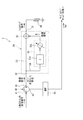
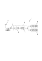
- FIG. 1 is a block diagram illustrating a receiving unit of a communication device according to an embodiment.
- a receiving unit 1 of a communication apparatus includes an antenna 2 for receiving a radio signal, a low noise amplifier 3 for amplifying a reception signal received by the antenna 2, and an analog to which a reception signal amplified by the low noise amplifier 3 is given.
- a digital converter 4 for amplifying a reception signal received by the antenna 2, and an analog to which a reception signal amplified by the low noise amplifier 3 is given.
- the analog-to-digital converter 4 (hereinafter also referred to as AD converter 4) is a digital signal in which a communication signal (analog input signal), which is an analog signal of a radio frequency, is represented by a 1-bit pulse train. The signal is converted into a signal, and the converted digital signal is given to a processing unit (not shown) that performs communication processing connected to a subsequent stage.
- the AD converter 4 includes a band pass filter (BPF: Band Pass filter) 5, a sample and hold circuit (S / H: Sample and Hold Circuit) 6, and a ⁇ (Delta Sigma) modulator (DSM: Delta Sigma Modulator). 7.
- BPF Band Pass filter
- S / H Sample and Hold Circuit
- DSM Delta Sigma Modulator
- the band pass filter 5 is connected to the low noise amplifier 3.
- the band-pass filter 5 is provided with the reception signal amplified by the low noise amplifier 3.
- the band pass filter 5 is configured such that a pass band that allows passage of a given signal can be adjusted.
- the pass band of the band pass filter 5 is adjusted so as to include the frequency band of the communication signal S RF (analog input signal) that is received by the receiving unit 1. Therefore, the band-pass filter 5 passes the communication signal S RF that is received by the receiving unit 1 among the received signals given from the low-noise amplifier 3, and is a sample-and-hold circuit connected to the subsequent stage of the band-pass filter 5. 6, the passed communication signal S RF is given.
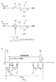
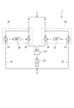
- FIG. 2A is a diagram showing an equivalent circuit of the sample and hold circuit 6. As shown in the figure, the sample-and-hold circuit 6 is connected via a branch path 12 to a switch 11 that connects and disconnects a line 10 that connects the bandpass filter 5 and the ⁇ modulator 7, and to a subsequent stage of the switch 11. And a capacitive element 13.
- the switch 11 interrupts the line 10 at the sampling frequency f SH .
- the communication signal S RF is given from the bandpass filter 5 to the ⁇ modulator 7 (sampling), and when the switch 11 is in the off state, it is given to the ⁇ modulator 7 by the capacitive element 13.
- the communication signal S RF is maintained (held).
- the sample and hold circuit 6 discretely samples the communication signal S RF that is a radio frequency analog signal supplied from the band pass filter 5 at the sampling frequency f SH .
- the sample and hold circuit 6 can sample and hold the communication signal S RF at the sampling frequency f SH to discretize the communication signal S RF in the time domain.
- the sample and hold circuit 6 gives the discretized communication signal S RF to the ⁇ modulator 7 as an output signal.
- the sample-and-hold circuit 6 can be considered to have given a square wave of low frequency f LO than the frequency of the communication signal S RF with respect to the communication signal S RF.
- Figure 2 (b) shows a sample and hold circuit 6 when considered giving a local signal of a rectangular wave of a low frequency f LO than the frequency of the communication signal S RF with respect to the communication signal S RF It is.
- the communication signal S RF is the local signal is mixed is a square wave of frequency f LO by the mixer 14, the communication signal S RF can be considered to be frequency converted to a lower frequency.
- the local signal given to the communication signal S RF includes a harmonic component having an odd multiple frequency such as 3f LO and 5f LO in addition to the signal component having the frequency f LO.
- the sample-and-hold circuit 6 performs frequency conversion by mixing a signal wave including a harmonic component such as 3f LO , 5f LO ... In addition to the signal component of the frequency f LO into the communication signal S RF . I can say that.
- the sampling frequency f SH of the sample and hold circuit 6 of the present embodiment is set lower than the center frequency f 0 of the communication signal S RF .
- the communication signal S RF is a signal having a predetermined bandwidth
- the center frequency f 0 of the communication signal S RF is 2.6 GHz
- a sampling frequency f SH of the sample-and-hold circuit 6 is assumed to be 100 MHz.
- the sample and hold circuit 6 has signal components such as 100 MHz, 300 MHz (third harmonic), 500 MHz (fifth harmonic), ... 2.5 GHz (25 th harmonic), 2.7 GHz (27 th harmonic),. It gives the signals containing wave to communication signals S RF.
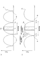
- FIG. 2C is a diagram showing a frequency spectrum of the communication signal S RF with a center frequency f 0 of 2.6 GHz, and shows a mode in which sampling and holding processing is performed with the sampling frequency f SH set to 100 MHz.
- the horizontal axis represents frequency and the vertical axis represents power.
- the communication signal S RF before frequency conversion is indicated by a solid line
- the communication signal S RF after frequency conversion is indicated by a broken line.
- the signal wave generated by the sample and hold circuit 6 includes a signal component that is an odd multiple of the sampling frequency f SH , and when this signal wave is mixed with the communication signal S RF , the center frequency f 0 is 2.
- the communication signal S RF of .6 GHz is frequency-converted to 100 MHz by the center frequency f 0 of the communication signal S RF by a signal component of 2.5 GHz (25th harmonic wave) included in the signal wave.
- the frequency conversion is performed so that the communication signal S RF having the center frequency f 0 of 2.6 GHz has a frequency lower than 200 MHz.
- the communication signal S RF is frequency-converted so as to have a frequency lower than 200 MHz, similarly to the communication signal S RF whose center frequency f 0 is 2.6 GHz.
- the communication signal S RF given to the sample and hold circuit 6 is a band W (band) divided by a plurality of harmonic frequency intervals included in the signal wave by the sample and hold circuit 6.
- width while being frequency-converted every 200 MHz) is twice the frequency of the sampling frequency f SH, frequency conversion such that the frequency in the frequency band from 0Hz to 200 MHz (twice the frequency of the sampling frequency f SH) Is done.
- the sampling frequency f SH of the sample-and-hold circuit 6, by setting lower than the communication signal S center frequency f 0 of the RF, the sample and hold circuit 6, the center frequency f 0 is the sampling frequency f SH
- the communication signal S RF given from the band pass filter 5 can be frequency-converted so that the frequency becomes lower than the doubled frequency.
- the sample-and-hold circuit 6 performs a process of sampling and holding the communication signal S RF at the sampling frequency f SH and discretizes the communication signal S RF in the time domain while sampling the center frequency f 0.
- the communication signal S RF that has been frequency-converted so as to have a frequency lower than twice the frequency f SH is supplied to the ⁇ modulator 7 as an output signal.
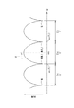
- FIG. 3 is a diagram illustrating an example of an equivalent circuit of the ⁇ modulator 7.
- the ⁇ modulator 7 receives the output signal of the sample and hold circuit 6 from the input terminal 20 as the input signal u, and outputs the output signal v after ⁇ modulation from the output terminal 21.
- the ⁇ modulator 7 includes a path 22 for feeding back the output signal v, a differencer 23 for obtaining a difference between the output signal v fed back by the path 22 and the input signal u, and an output signal v obtained by the differencer 23.
- a portion indicated by a broken line including the subtractor 23, the band pass filter 24, and the adder 25 constitutes a loop filter.
- the output signal v is expressed as the following equation (1).
- v u + Q (1) Therefore, the output of the differentiator 23 is expressed as the following equation (2).
- the output of the differentiator 23 is obtained by inverting the sign of the noise component Q included in the output signal v, and has an inverse characteristic of the noise component Q.
- the band pass filter 24 is configured such that a pass band that allows passage of a given signal can be adjusted.
- the pass band of the band pass filter 24 is adjusted to include the frequency band of the communication signal S RF given from the sample and hold circuit 6.
- the band-pass filter 24 passes the portion of the frequency band including the frequency band of the communication signal S RF among the inverse characteristics of the noise component Q, and gives it to the adder 25.
- the noise component including the quantization noise is suppressed by adding the inverse characteristic of the noise component Q.
- the band (quantization noise blocking band) for passing the communication signal S RF and blocking the quantization noise is determined by the pass band of the band pass filter 24.
- .DELTA..SIGMA modulator 7 a communication signal S RF that exist within the frequency band from 0Hz to twice the frequency of the sampling frequency f SH including a communication signal S RF having a predetermined bandwidth
- Output signal v is output.
- the output signal v is output as a digital signal representing the communication signal S RF as a 1-bit pulse train (pulse signal).
- the sampling frequency f s of the ⁇ modulator 7 of this embodiment is set higher than a value obtained by doubling the sampling frequency f SH of the sample and hold circuit 6.
- the sampling frequency f SH of the sample-and-hold circuit 6 is set as a value obtained by the sampling frequency f SH of the sample-and-hold circuit 6 is doubled is lower than the sampling frequency f s of the ⁇ modulator 7 ing.
- the sampling frequency f s of the ⁇ modulator 7 is set according to the frequency bandwidth of the communication signal S RF . For example, if the frequency bandwidth of the communication signal S RF is 20 MHz, the sampling frequency f s of the ⁇ modulator 7 is set to 2 GHz, which is 100 times (oversampling rate is 50 times).
- the sampling frequency f s of the ⁇ modulator 7 is determined according to the bandwidth of the communication signal S RF , first, the sampling frequency f s of the ⁇ modulator 7 is set. Thereafter, the sampling frequency f SH of the sample and hold circuit 6 is set to be lower than the sampling frequency f s of the ⁇ modulator 7.
- the ⁇ modulator 7 can suitably perform ⁇ modulation by setting the center frequency f 0 of the communication signal S RF that is the object of ⁇ modulation to be lower than the sampling frequency f s .
- the sampling frequency f SH of the sample and hold circuit 6 is set lower than the center frequency f 0 of the communication signal S RF when the sample and hold circuit 6 is given, communication is performed.
- the signal S RF is frequency-converted by the sample and hold circuit 6 so that the center frequency f 0 is lower than a value obtained by doubling the sampling frequency f SH of the sample and hold circuit 6.
- the sampling frequency f s of the ⁇ modulator 7 set higher than the value obtained by doubling the sampling frequency f SH of the sample and hold circuit 6 is set smaller than the center frequency f 0 of the communication signal S RF. It will never be done.
- the sampling frequency f SH so that the value obtained by doubling the sampling frequency f SH of the sample and hold circuit 6 is lower than the sampling frequency f s of the ⁇ modulator 7.
- the center frequency f 0 of the communication signal S RF can be surely set lower than the sampling frequency f s .
- the sample and hold circuit 6 converts the frequency of the communication signal S RF so that the center frequency f 0 is lower than the frequency obtained by doubling the sampling frequency f SH of the sample and hold circuit 6. can do. Therefore, the sampling frequency f SH of the sample-and-hold circuit 6, that the sampling frequency f SH of the sample-and-hold circuit 6 is a value obtained by doubling is set to a value larger than the bandwidth of the communication signal S RF preferable. Thereby, the sample and hold circuit 6 changes the communication signal S RF so that the communication signal S RF becomes a signal in a frequency band lower than the frequency obtained by doubling the sampling frequency f SH of the sample and hold circuit 6. Frequency conversion can be performed.
- the AD converter 4 having the above configuration includes a sample-and-hold circuit 6 to which an analog input signal is given, a band-pass ⁇ modulator 7 that ⁇ -modulates an output signal output from the sample-and-hold circuit 6 and outputs it as a digital signal, It has.
- the sampling frequency f SH of the sample and hold circuit 6 is set lower than the center frequency f 0 of the analog input signal.
- the sample and hold circuit 6 is discretizing the communication signal S RF.
- the center frequency f 0 of the communication signal S RF can be converted to a lower frequency and output.
- a signal converted to a lower center frequency f 0 and discretized can be supplied to the ⁇ modulator 7, and ⁇ modulation
- the device 7 can perform an appropriate operation.
- the AD converter 4 capable of appropriate operation can be obtained.
- the sample and hold circuit 6 converts the frequency of the communication signal S RF so that the center frequency f 0 is lower than the frequency obtained by doubling the sampling frequency f SH of the sample and hold circuit 6. Can do. That is, even if the communication signal S RF before the frequency conversion is in any frequency band, the communication signal S RF has a center frequency f 0 higher than the frequency obtained by doubling the sampling frequency f SH of the sample and hold circuit 6. Is also converted to be within a lower frequency band. For this reason, the quantization noise stop band of the ⁇ modulator 7 can be adjusted in a frequency range lower than a value obtained by doubling the sampling frequency f SH of the sample and hold circuit 6.
- the ⁇ modulator 7 can perform ⁇ modulation on the communication signal SRF in any frequency band regardless of the frequency band before frequency conversion. That is, the receiving unit 1 of the present embodiment can receive and digitally convert multiband regardless of the frequency band of the communication signal SRF .
- the band-pass filter 5 and the band-pass filter 24 according to the present embodiment are configured so that a pass band that allows passage of a given signal is adjustable (tunable).
- the bandpass filters 5 and 24 configured to be tunable will be described.
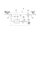
- FIG. 4 is a block diagram showing an example of the configuration of the bandpass filter 5. Since the band pass filter 24 can be configured in the same manner as the band pass filter 5, only the band pass filter 5 will be described here.
- the bandpass filter 5 includes a filter circuit 30 and a circulator 40.
- the circulator 40 is connected with the low-noise amplifier 3 at the front stage, the sample-and-hold circuit 6 at the rear stage, and the filter circuit 30.
- the reception signal given from the low noise amplifier 3 passes through the circulator 40 and is given to the filter circuit 30.
- the filter circuit 30 performs a process of blocking a signal near the center frequency f 0 of the communication signal S RF included in the received signal and allowing other signals to pass through the given received signal. That is, the filter circuit 30 has a function as a band elimination filter (notch filter) that blocks passage of a signal in the vicinity of the center frequency f 0 of the communication signal S RF .
- notch filter band elimination filter
- a terminating resistor element 46 having one end connected to the output end 31 of the filter circuit 30 and the other end grounded is connected to the subsequent stage of the filter circuit 30. The signal that has passed through the filter circuit 30 is terminated by the termination resistance element 46.
- the circulator 40 has three ports.
- the low noise amplifier 3 is connected to the first port 41.
- the filter circuit 30 is connected to the second port 42.
- a sample and hold circuit 6 is connected to the third port 43.
- the circulator 40 is configured to output a signal given from the first port 41 from the second port 42 and to output a signal given from the second port 42 from the third port 43, and a signal is sent to the circulator 40. Signal transmission is performed irreversibly according to a given port.
- a signal in the vicinity of the center frequency f 0 including the communication signal S RF is given to the second port 42 of the circulator 40 by being reflected by the filter circuit 30.
- the circulator 40 outputs a signal near the center frequency f 0 including the communication signal S RF given to the second port 42 from the third port 43.
- a signal in the vicinity of the center frequency f 0 including the communication signal S RF output from the third port 43 of the circulator 40 is given to the sample and hold circuit 6 after passing through the band-pass filter 45.
- the filter circuit 30 has a function as a band elimination filter (notch filter), and the band in which the filter circuit 30 prevents the signal from passing is the communication signal S RF having the center frequency f 0. It is set to include the frequency band. Further, the filter circuit 30 is adjustable (tunable) in the band (center frequency) in which the filter circuit 30 blocks the passage of signals.
- notch filter band elimination filter
- the filter circuit 30 filters the received signal as an input signal given to the input terminal 32 via the circulator 40, and outputs the filtered filtering signal from the output terminal 31.
- the filter circuit 30 synthesizes the processing unit 35 provided on the branch line 34 branched from the signal line 33 through which the received signal passes, and the pulse signal that has passed through the signal line 33 and the processing signal output from the processing unit 35. And a synthesizer 36.
- the processing unit 35 includes a delay element 35a and a phase shifter 35b.
- the delay element 35a has a function of performing a delay process for delaying the pulse signal.
- the phase shifter 35b has a function of performing a phase shift process for shifting the phase of the received signal by a predetermined phase amount. That is, the processing unit 35 generates a delayed signal delayed from the reception signal given from the low noise amplifier 3 as a processing signal.
- a notch is generated in the frequency domain of the received signal wave.
- the notch has a smaller gain than the gain in the frequency band around the notch, and the gain change appears as a very steep characteristic.
- the notch since the notch is caused by interference between the direct wave and the delayed wave, it periodically appears on the frequency domain regardless of the level of the frequency.
- the filter circuit 30 generates a delayed signal delayed from the received signal from the low noise amplifier 3 so as to use the notch as described above for the filtering process, and synthesizes the generated delayed signal and the received signal. To do. Thereby, the filter circuit 30 generates a notch on the frequency domain of the synthesized signal, and outputs a filtered signal obtained by performing the filtering process on the received signal. In other words, the filter circuit 30 uses a notch appearing in this frequency region to block the passage of a signal in a specific frequency band and allows the signal to pass in a frequency band other than the notch.
- FIG. 5 is a diagram illustrating an example of the filter characteristics of the filter circuit 30.
- the horizontal axis indicates angular frequency
- the vertical axis indicates gain.
- a plurality of notches N appear periodically in the filter characteristics of the filter circuit 30. Since the notch N is generated by synthesizing the received signal and the processing signal which is the delayed wave, a plurality of notches N periodically appear according to the phase of both signals.
- the filter circuit 30 is configured such that the position of the notch N appearing as the filter characteristic of the filter circuit 30 in the frequency domain can be adjusted.
- the adjustment of the position of the frequency domain of the notch N in FIG. 5, the notch N of the angular frequency .omega.1 (hereinafter, first referred to as a notch N 1) and, of angular frequency ⁇ 2 notch N (hereinafter, a second notch N 2 )).
- f (t) represents the received signal given to the filter circuit 30 in the time domain
- f (t ⁇ ) represents the processed signal that is a delayed signal output from the processing unit 35 in the time domain.
- t is time
- ⁇ is a delay amount (delay time) of the processing signal with respect to the received signal.
- the filtering signal obtained by combining these can be expressed as the following equation (3). f (t) + [waveform obtained by shifting f (t ⁇ ) by the carrier phase ⁇ ] (3)
- F ( ⁇ ) represents the received signal in the frequency domain
- ⁇ is the angular frequency
- ⁇ is the phase amount indicating the phase difference of the processed signal with respect to the received signal (the carrier wave in equation (3)) The same as phase ⁇ ).
- ⁇ + ⁇ represents the phase of the filtered signal
- the phase of the first notch N 1 is the angular frequency omega 1
- the second phase at the notch N 2 is the angular frequency omega 2 2 [pi
- ⁇ 1 ⁇ + ⁇ 2n ⁇ (6)
- ⁇ 2 ⁇ + ⁇ 2 (n + 1)
- ⁇ (7) ⁇ 2 ⁇ ⁇ 1 2 ⁇ / ⁇ (8)
- a first notch N 1 the frequency bandwidth between the second notch N 2 can be represented by the amount of delay tau. From the above equation (8), it can be seen that the interval between the notches adjacent to each other on the frequency region can be set by the delay amount ⁇ .
- the phase amount ⁇ can be expressed by ⁇ 0 and the delay amount ⁇ . That is, the phase amount ⁇ can be obtained from ⁇ 0 and the delay amount ⁇ . Therefore, for example, at an angular frequency ⁇ 0 between the first notch N 1 and the second notch N 2 with respect to a position on an arbitrary frequency region such as a carrier frequency of the frequency of the RF signal included in the pulse signal.
- the phase amount ⁇ can be adjusted.
- the phase amount ⁇ is a value for setting the center frequency between the first notch N 1 and the second notch N 2 to ⁇ 0
- the phase amount ⁇ is the value of the first notch N 1 and the second notch N 2 . Parameters for setting the position on the frequency domain are configured.
- the filter circuit 30 can adjust the position of the notch N in the frequency domain by adjusting the delay amount ⁇ of the processing signal output from the processing unit 35 and the phase amount ⁇ . That is, the delay element 35a and the phase shifter 35b can adjust the position of the notch N appearing in the frequency domain of the filtering signal on the frequency domain by adjusting the delay quantity ⁇ in the delay process and the phase quantity ⁇ in the phase shift process.
- the delay amount ⁇ is determined by the above equation (8).
- the phase amount ⁇ can be obtained by substituting the determined delay amount ⁇ into the above equation (10).
- the phase amount ⁇ in the above formula (10) is a value for setting the center frequency between the first notch N 1 and the second notch N 2 to ⁇ 0 , so the position of the notch N in the frequency region is
- the first notch N 1 and the second notch N 2 are set so that the center frequency f 0 is positioned between the first notch N 1 and the second notch N 2 .
- a value obtained by adding or subtracting a half value of the bandwidth between the first notch N 1 and the second notch N 2 to the center frequency f 0 and further multiplying by 2 ⁇ is expressed by the above formula ( Substitute as ⁇ 0 of 10).
- the delay amount ⁇ and the phase amount ⁇ for arbitrarily setting the position of the notch N in the frequency region can be obtained.
- the delay amount ⁇ of the processing signal is adjusted by the delay element 35a of the processing unit 35. Further, the phase amount ⁇ of the processing signal is adjusted by the phase shift processing by the phase shifter 35 b of the processing unit 35.
- a band (stop band) in which the filter circuit 30 blocks signal passage is set according to the center frequency f 0 of the communication signal S RF .
- the delay element 35a and the phase shifter 35b of the processing unit 35 adjust the delay amount ⁇ and the phase amount ⁇ so that a stop band set according to the center frequency f 0 of the communication signal S RF is realized.
- the first notch N 1 is set as the required bandwidth is set according to the frequency bandwidth between the second notch N 2. Further, the phase amount ⁇ of the phase shifter 35b is set according to the set frequency corresponding to the filter processing.
- FIG. 6 is a diagram showing a part of the frequency spectrum of the reception signal output from the low noise amplifier 3, and shows the relationship with the filter characteristics of the filter circuit 30.
- a diagram P shows the filter characteristics of the filter circuit 30.
- the horizontal axis represents frequency and the vertical axis represents power.
- the received signal includes a communication signal S RF having a center frequency f 0 .
- the filter circuit 30 of the present embodiment the communication signal the position of the frequency domain of the notch N appearing in the diagram P showing the filter characteristic of the filter circuit 30 S RF center frequency f
- the delay amount ⁇ of the processing signal and the phase amount ⁇ are adjusted so as to be zero .
- the filter circuit 30 is set so as to prevent the communication signal S RF having the center frequency f 0 from passing therethrough and allow the signal to pass in other frequency bands.
- the filter circuit 30 sets a stop band that blocks signal passage in a fixed bandwidth centered on the position of the notch N on the frequency region. Therefore, the center frequency of the stop band substantially coincides with the position of the notch N on the frequency region.
- the center frequency of the stop band is set so as to substantially coincide with the center frequency f 0.
- the stop band is set so as to include the frequency band of the communication signal SRF .
- the filter circuit 30 has a function as a band elimination filter for blocking passage of the center frequency f 0 near the signal (notch filter).
- the filter circuit 30 blocks passage of noise components at positions on the frequency region corresponding to the other notches N in addition to the main signal component (RF signal).
- a signal that passes through the filter circuit 30 and is output as a filtering signal from the filter circuit 30 is terminated by the termination resistance element 46 (FIG. 4).
- the communication signal S RF blocked by the filter circuit 30 and the noise component at the position corresponding to the notch N are reflected by the filter circuit 30 and returned to the circulator 40 (FIG. 4).
- the signal component reflected by the filter circuit 30 is output from the third port 43 of the circulator 40 and given to the bandpass filter 45.
- the band pass filter 45 is configured to pass the communication signal S RF having the center frequency f 0 and to block the noise components at positions corresponding to the other notches N. As a result, the communication signal SRF is given to the sample and hold circuit 6 provided in the subsequent stage of the band pass filter 45, and unnecessary noise components are prevented from being given.
- the band pass filter 45 may be omitted.
- the position of the notch appearing in the filter characteristics (on the frequency domain of the filtering signal) of the filter circuit 30 on the frequency domain is determined based on the delay amount ⁇ of the delay element 35a and the phase amount ⁇ of the phase shifter 35b. Therefore, the position of the notch on the frequency region can be set to a set frequency set according to the filter processing, and the stop band can be set to a desired band by using the notch.
- the band-pass filter 5 that the stop band of the filter circuit 30 is adjusted to include the band of the communication signal S RF, taken out a communication signal S RF in the filter circuit 30 is reflected, giving a sample and hold circuit 6.
- the bandpass filter 5 has a function as a bandpass filter, and is configured such that the passband can be adjusted (tunable) by adjusting the stopband of the filter circuit 30.
- FIG. 7 is a block diagram illustrating another example of the configuration of the bandpass filter 5.
- the bandpass filter 5 includes a first filter circuit unit 51, a second filter circuit unit 52, a third filter circuit unit 53, and a bandpass filter (BPF) 54.
- BPF bandpass filter
- FIG. 8 is a block diagram showing a configuration of the first filter circuit unit 51.
- the first filter circuit unit 51 performs a filtering process on the received signal from the low noise amplifier 3 given to the input terminal 55, and outputs the filtered filtering signal from the output terminal 56.
- the first filter circuit unit 51 includes a processing unit 35 provided on a branch line 58 branched from a signal line 57 through which a reception signal passes, a reception signal that has passed through the signal line 57, and a processing signal output by the processing unit 35.
- the power combiner 36 is configured to be combined with the filter circuit 30 described above.
- the first filter circuit unit 51 gives the filtered signal obtained by performing the filtering process on the received signal to the second filter circuit unit 52 provided in the subsequent stage.
- the second filter circuit unit 52 and the third filter circuit unit 53 have the same configuration as the filter circuit 30 described above. Therefore, when the filtering signal from the first filter circuit unit 51 is given, the second filter circuit unit 52 is provided with a third filter provided in a subsequent stage with a filtering signal obtained by further filtering the given filtering signal. This is given to the circuit unit 53.
- the third filter circuit unit 53 When the third filter circuit unit 53 receives the filtering signal from the second filter circuit unit 52, the third filter circuit unit 53 applies a filtered signal obtained by further filtering the received filtering signal to a bandpass filter 54 provided in the subsequent stage. give. The filtering signal applied to the band pass filter 54 is then applied to the sample and hold circuit 6.
- the band-pass filter 5 is configured to perform filter processing in multiple stages on the received signal by the plurality of filter circuit units 51, 52, and 53.
- each filter circuit unit 51, 52, 53 adjusts the delay amount ⁇ of the processing signal output from the processing unit 35 and the phase amount ⁇ to adjust the frequency on the notch N.
- the position can be adjusted.
- the delay amount ⁇ of the processing signal is adjusted by the delay element 35a of the processing unit 35.
- the phase amount ⁇ of the processing signal is adjusted by the phase shifter 35 b of the processing unit 35.
- FIG. 9A is a diagram illustrating the relationship between the frequency spectrum of the reception signal output from the low noise amplifier 3 and the filter characteristics of the first filter circuit unit 51.
- the horizontal axis represents frequency and the vertical axis represents power.
- the band-pass filter 5 is set to have a function as a band-pass filter that passes the communication signal S RF having the center frequency f 0 .
- the first filter circuit 51, the position of the frequency domain of the notch N appearing in the diagram P1 showing the filter characteristic of the first filter circuit portion 51 does not overlap the center frequency f 0 of the communication signal S RF Have been adjusted so that.
- the notch N appearing in the filter characteristic of the first filter circuit portion 51 is positioned on either side of the center frequency f 0.
- a pair of notches N which are adjacent to each other are located so as to sandwich the main signal component of the center frequency f 0.
- the delay amount ⁇ of the processing signal and the phase amount ⁇ are adjusted so that the pair of notches N are positioned with the communication signal S RF having the center frequency f 0 interposed therebetween.
- a pair of notches N sandwiching the communication signal S RF setting the frequency of the notch N which is set to a higher frequency side than the center frequency f 0 was set to include the center frequency f 0 band in the vicinity The upper limit frequency f U1 of the set band is set.
- the set frequency of the notch N set on the frequency side lower than the center frequency f 0 is set to appear at the lower limit frequency f L1 of the set band. Yes.
- the set band is a band set so as to include a permissible pass band that is desired to be allowed to pass in the frequency band of the received signal.
- the pass allowable band is the frequency band of the communication signal SRF .
- the bandwidth of the set band is set in advance according to the communication signal SRF , the state of the noise component, and the like.
- the center frequency of the set band is set so as to substantially coincide with the center frequency f 0 of the communication signal S RF that constitutes the allowable pass band.
- the first filter circuit unit 51 allows the communication signal S RF having the center frequency f 0 to pass, blocks the signal in the vicinity of the notch N, and gives the output filtered signal to the second filter circuit unit 52. .
- FIG. 9B is a diagram illustrating the filter characteristics of the second filter circuit unit 52, and is a diagram illustrating the relationship between the stop band of the first filter circuit unit 51 and the stop band of the second filter circuit unit 52.
- the notch N appearing in the diagram P2 showing the filter characteristics of the second filter circuit 52, similarly to the first filter circuit portion 51, are located on either side of the center frequency f 0.
- the delay amount ⁇ of the processing signal and the phase amount ⁇ are adjusted so that the pair of notches N are positioned with the communication signal S RF having the center frequency f 0 interposed therebetween.
- the set band of the second filter circuit unit 52 is set wider than the set band of the first filter circuit unit 51.
- the center frequency of the set band, similar to the first filter circuit portion 51 is set so as to substantially coincide with the communication signal S RF center frequency f 0. Therefore, the set frequency of the notch N that is set on the frequency side higher than the center frequency f 0 among the pair of notches N sandwiching the communication signal S RF in the filter characteristics of the second filter circuit unit 52 is the first filter circuit unit.
- the upper limit frequency f U2 is set to be higher than the upper limit frequency f U1 in the 51 setting band.
- the set frequency of the notch N set on the frequency side lower than the center frequency f 0 among the pair of notches N sandwiching the communication signal S RF is lower than the lower limit frequency f L1 in the set band of the first filter circuit unit 51. Is set to the lower limit frequency f L2 , which is a lower frequency.
- the notch N of the second filter circuit unit 52 is a notch N (adjacent notch) set by the first filter circuit unit 51 adjacent in the frequency domain to a part of the stop band where the notch N blocks signal passage. ) Is set to overlap with a part of the stop band. Thereby, the noise component in the vicinity of the communication signal S RF is removed by the stop band of the first filter circuit unit 51 and the stop band of the second filter circuit unit 52.
- the bandwidth of the set band of the second filter circuit unit 52 is set in advance according to the communication signal SRF , the bandwidth of the set band of the first filter circuit unit 51, and the like.
- the second filter circuit unit 52 allows the communication signal S RF having the center frequency f 0 to pass, blocks the signal in the stop band due to the notch N, and outputs the filtered signal as the output to the third filter circuit unit 53. To give.
- the set band of the third filter circuit unit 53 is set wider than the set band of the second filter circuit unit 52.
- the third filter circuit 53 can eliminate the noise components of the band remote from the further communication signal S RF than stopband by other filter circuitry 51 and 52.
- the third filter circuit unit 53 gives the filtered signal obtained as described above to the band-pass filter 54.
- the band pass filter 54 is configured to pass the communication signal S RF and to block other noise components. As a result, the communication signal S RF is given to the sample and hold circuit 6 provided in the subsequent stage of the band pass filter 54.
- the band pass filter 54 can be omitted.
- Band-pass filter 5 by adjusting the stop band of the filter circuit portions 51, 52, 53, passed through a communication signal S RF in the filter circuit portions 51, 52, and 53 while removing the noise components, the sample-and This is given to the hold circuit 6.
- the band pass filter 5 is configured such that the pass band can be adjusted (tunable) by adjusting the stop bands of the filter circuit units 51, 52, and 53.
- the received signal (communication signal S RF ) received by the antenna 2 may include a plurality of signal components (frequency components).
- FIG. 10A is a diagram illustrating a frequency spectrum when a plurality of signal components are included in the reception signal received by the antenna 2.
- the horizontal axis represents frequency and the vertical axis represents power.
- the signal component before frequency conversion is indicated by a solid line, and the signal component after frequency conversion is indicated by a broken line.
- FIG. 10A shows a case where a plurality of (two in the illustrated example) signal components (first signal component S RF1 and second signal component S RF2 ) are included in the received signal received by the antenna 2. ing.
- the reception signal received by the antenna 2 is given to the band pass filter 5 of the AD converter 4 through the low noise amplifier 3.
- the band-pass filter 5 of the AD converter 4 passes the communication signal that is received by the receiving unit 1 among the received signals supplied from the low noise amplifier 3 and passes it to the sample and hold circuit 6. It is comprised so that the made communication signal may be given.
- the pass band of the band pass filter 5 is set to prevent the second signal component S RF2 from passing. if it is, the band-pass filter 5, passes only the first signal component S RF1, the sample and hold circuit 6, only the first signal component S RF1 is given. Subsequent processing is as described above.
- the sample and hold circuit 6 is provided with both signal components S RF1 and S RF2. .
- the sampling frequency f SH of the sample and hold circuit 6 is the frequency f 11 .
- the center frequency f 0 1 of the first signal component S RF1 exists in a band W 1 between a frequency n times the frequency f SH1 and a frequency (n + 2) times the frequency f 11 and the band W 1.
- the center frequency f 0 2 of the second signal component S RF2 is a (n + 2) times the frequency of the frequency f 11, the frequency f 11 and (n + 4) times the frequency of the consider the case to match the center frequency of the band W 2 together are present in the band W 2 of.
- n is a predetermined odd number.
- the sample if-and-hold circuit 6 converts the frequency of the first signal component S RF1, the first signal component S RF1, the sample-and-hold n-th wave signal components that are included in the signal wave circuit 6 (frequency of nf 11 The harmonic frequency is converted so that the center frequency f 0 1 becomes the same frequency f 11 as the sampling frequency f SH of the sample and hold circuit 6.
- the center frequency f 0 2 of the second signal component S RF2 is the center frequency of the band W 2 , the frequency is (n + 2) f 11 + f 11 . Therefore, the sample-and-hold circuit 6 converts the frequency of the second signal component S RF2, the second signal component S RF2 is included in the signal wave of the sample and hold circuit 6 is (n + 2) times wave signal component (frequency ( n + 2f 11 )) is converted so that the center frequency f 0 2 becomes the same frequency f 11 as the sampling frequency f SH of the sample and hold circuit 6.
- both signal components S RF1 and S RF2 after the frequency conversion become the same center frequency f 11 and overlap. If the sample and hold circuit 6 gives a signal in which both signal components S RF1 and S RF2 are overlapped to the ⁇ modulator 7, the ⁇ modulator 7 cannot separate the overlapped signal components S RF1 and S RF2. The signal component cannot be extracted and converted to a digital signal.
- the sample and hold circuit 6 By adjusting the sampling frequency f SH of the sample and hold circuit 6, the frequency-converted communication signals S RF1 and S RF2 included in the output signal output from the sample and hold circuit 6 are set to different frequencies. It is possible to output in a separated state.
- a sample and hold circuit is used. 6 adjusts the sampling frequency f SH of the sample and hold circuit 6.
- the sample and hold circuit 6 adjusts the sampling frequency f SH from the frequency f 11 in FIG. 10A to a frequency f 12 that is higher than the frequency f 11 by f d .
- FIG. 10B is a diagram showing a frequency spectrum when the sampling frequency f SH of the sample and hold circuit 6 is adjusted from the state of FIG.
- the horizontal axis represents frequency and the vertical axis represents power.
- the signal component before frequency conversion is indicated by a solid line, and the signal component after frequency conversion is indicated by a broken line.
- the frequency 2f 12 which is the upper limit of the frequency band is present frequency-converted signal components in FIG. 10 (a), the which is the upper limit of the frequency band is present frequency-converted signal component frequency against 2f 11, it has a higher frequency is only 2f d.
- the center frequency f 0 1 of the first signal component S RF1 is present in the band W 3 between the m times the frequency of the frequency f 12, the frequency f 12 and (m + 2) times the frequency and is, also, the center frequency f 0 2 of the second signal component S RF2 is a (m + 2) times the frequency of the frequency f 12, the band W 4 between the (m + 4) times the frequency of the frequency f 12 Existing.
- m is a predetermined odd number.
- the center frequency f 0 1 of the first signal component S RF1 coincides with the center frequency of the band W 3 , the center frequency f 0 1 is mf 12 + f 12 . Therefore, the first signal component S RF1 has a center frequency f 0 1 of the sample-and-hold circuit 6 due to the m-th harmonic signal component included in the signal wave of the sample-and-hold circuit 6 (a harmonic having a frequency of mf 12 ). Frequency conversion is performed so that the frequency f 12 is the same as the sampling frequency f SH .
- the center frequency f 0 2 of the second signal component S RF2 is offset in the direction of a lower frequency with respect to the center frequency of the band W 4 .
- the sample-and-hold circuit 6 converts the frequency of the second signal component S RF2, the second signal component S RF2 is included in the signal wave of the sample and hold circuit 6 (m + 2) is frequency doubled signal components (frequency ( the m + 2) harmonic f 12), the center frequency f 0 2 is frequency converted to a lower frequency f 13 than the frequency f 12 of the sampling frequency f SH.
- the first signal component S RF1 and the second signal component S RF2 are separated such that their center frequencies are different from each other.
- the sample and hold circuit 6 adjusts the sampling frequency f SH of the sample and hold circuit 6 to change the frequency of the plurality of signal components S RF1 and S RF2.
- the frequency interval of harmonics included in the signal wave given to the communication signal from 6 can be changed.
- the bandwidth of the band W divided by the frequency interval of the harmonics is changed, and the frequency direction positions of the plurality of signal components S RF1 and S RF2 after the frequency conversion are moved relative to each other. Can be separated.
- the ⁇ modulator 7 selects at least one of a plurality of frequency-converted signal components S RF1 and S RF2 included in the output signal output from the sample and hold circuit 6 and performs ⁇ modulation so as to perform ⁇ modulation.
- the quantization noise stop band of the device 7 is adjusted.
- the ⁇ modulator 7 selects the first signal component S RF1 that is a communication target, performs ⁇ modulation, and outputs a digital signal corresponding thereto.
- the communication signal S RF including the plurality of signal components S RF1 and S RF2 is given to the sample and hold circuit 6, a necessary signal component is selected and the selected signal component is selected. Can be converted into a digital signal.
- FIG. 11 is a diagram illustrating an equivalent circuit of a ⁇ modulator included in a receiving unit of a communication device according to another embodiment.
- the ⁇ modulator 7 of the present embodiment includes two loop filters, and a sample and hold circuit 6 is provided with a communication signal S RF including a plurality of signal components S RF1 and S RF2 having different center frequencies, and is sampled.
- a communication signal S RF including a plurality of signal components S RF1 and S RF2 having different center frequencies, and is sampled.
- ⁇ modulation is performed on each of the plurality of signal components S RF1 and S RF2 ,
- One digital signal including the signal components S RF1 and S RF2 is output.
- the ⁇ modulator 7 receives the output signal of the sample and hold circuit 6 as an input signal u, and distributes the input signal u to both the loop filters 28 and 29. Both loop filters 28 and 29 are provided with distribution signals u 1 and u 2 obtained by distributing the input signal u, and also with an output signal v fed back from the path 22.
- the ⁇ modulator 7 includes an adder 27 that adds the outputs of both loop filters 28 and 29 to each other.
- the adder 27 adds the outputs of both the loop filters 28 and 29 to each other and then gives the added output to the quantizer 26 connected to the subsequent stage of the adder 27.
- the quantizer 26 of the present embodiment is composed of a two-level quantizer.
- the quantizer 26 quantizes the output given from the adder 27 and outputs an output signal v.
- the output signal v is a digital signal represented as a 1-bit pulse train (pulse signal) including both signal components S RF1 and S RF2 .
- FIG. 12 is a block diagram illustrating a receiving unit of a communication apparatus including the ⁇ modulator 7 illustrated in FIG.
- a first processing unit 8 and a second processing unit 9 are connected to the AD converter 4 in the subsequent stage.
- the first processing unit 8 has a function of performing communication processing of the first signal component SRF1 .
- the second processing unit 9 has a function of performing communication processing of the second signal component SRF2 .
- the sample and hold circuit 6 outputs the output that the sample and hold circuit 6 outputs.
- the plurality of signal components S RF1 and S RF2 after frequency conversion included in the signal are output in a state of being separated from each other, and the ⁇ modulator 7 further outputs ⁇ for each of the plurality of signal components S RF1 and S RF2 . Modulate and output one digital signal.
- each of the plurality of signal components S RF1 and S RF2 can be converted into a digital signal and used.
- the AD converter 4 separates the plurality of signal components S RF1 and S RF2 and is necessary. This is because a signal component can be selected or converted into a digital signal for each of a plurality of separated signal components.
- the reception unit 1 can pass the signal component to be received, and give the signal component to be received to the sample and hold circuit 6.
- the received signal received by the antenna 2 includes a plurality of signal components, only the necessary signal components are selected, and the signals necessary for the sample-and-hold circuit 6 and the ⁇ modulator 7 are selected. Ingredients can be given. Further, by suppressing the application of unnecessary signal components, the sample-and-hold circuit 6 and the ⁇ modulator 7 can omit processing such as separation and selection of a plurality of signal components.
- the bandpass filter 5 and the bandpass filter 24 included in the ⁇ modulator 7 in the above embodiment can be configured such that the passband is controlled by a control unit (not shown), for example.
- the control unit acquires information about the communication signal S RF such as the frequency band of the communication signal S RF included in the reception signal received by the antenna 2 from the reception signal received by the antenna 2 or the outside, and acquires the acquired communication signal. It is possible to control the pass band of the band-pass filter 24 having the band-pass filter 5 and the ⁇ modulator 7 based on the information about the S RF.
- the band-pass filter 5 (24) includes three filter circuit units.
- the filter may be configured with one filter circuit unit, or four or more. It can also be configured with many filter circuit sections.
Landscapes
- Engineering & Computer Science (AREA)
- Theoretical Computer Science (AREA)
- Compression, Expansion, Code Conversion, And Decoders (AREA)
Abstract
アナログデジタル変換器4はアナログ入力信号が与えられるサンプルアンドホールド回路6と、サンプルアンドホールド回路6が出力する出力信号をΔΣ変調しデジタル信号として出力するバンドパス型のΔΣ変調器7とを備えている。サンプルアンドホールド回路6のサンプリング周波数fSHは、アナログ入力信号の中心周波数f0よりも低く設定されている。
Description
本発明は、AD変換器及びこれを用いた通信装置に関する。
近年、携帯電話等の無線通信システムにおいては、高速化を目的として広帯域化が進んでおり、より広い周波数帯域を確保するために無線周波数が高周波化される傾向にある。
その一方、通信装置においては、装置の小型化等を目的として、できるだけアナログ処理の要素を排除し、信号処理をできるだけデジタル領域で行おうとする試みがなされている。
このため、上記無線通信システムで用いられる通信装置においては、高周波のアナログ入力信号をデジタル処理する機能が求められている。
このため、上記無線通信システムで用いられる通信装置においては、高周波のアナログ入力信号をデジタル処理する機能が求められている。
例えば、一般的なアナログデジタル変換器を用いてアナログ入力信号をデジタル信号に変換する場合、アナログ入力信号の周波数の2倍以上のサンプリング周波数のアナログデジタル変換器を用いる必要がある。
このため、例えば、無線周波数が2.6GHz、帯域幅20MHzといったLTE等の高周波のアナログ入力信号をデジタル信号に変換する場合、サンプリング周波数が5GHz以上といったような非常に高いサンプリング周波数のアナログデジタル変換器を用いなければならないおそれがある。
このため、例えば、無線周波数が2.6GHz、帯域幅20MHzといったLTE等の高周波のアナログ入力信号をデジタル信号に変換する場合、サンプリング周波数が5GHz以上といったような非常に高いサンプリング周波数のアナログデジタル変換器を用いなければならないおそれがある。
そこで、バンドパス型ΔΣ変調器を利用したアナログデジタル変換器を用いることが考えられる。バンドパス型ΔΣ変調器では、サンプリング周波数は、信号の中心周波数ではなく、信号の帯域幅に対してオーバサンプリングとなるように設定される(例えば、特許文献1参照)。
このため、無線周波数が2.6GHz、帯域幅20MHzといった上述のアナログ入力信号をデジタル信号に変換する場合、バンドパス型ΔΣ変調器のサンプリング周波数は、帯域幅20MHzの100倍程度の2GHzに設定すればよい。これによって、サンプリング周波数が極端に高く設定されるのを抑制することができる。
上記バンドパス型ΔΣ変調器を利用したアナログデジタル変換器では、サンプリング周波数がデジタル入力信号の帯域幅に対してオーバサンプリングとなるように設定すればよい。これによって、サンプリング周波数が極端に高くなるのを抑制できる。
一方、アナログ入力信号の中心周波数との関係においては、バンドパス型ΔΣ変調器のサンプリング周波数はアナログ入力信号の中心周波数よりも高いことが好ましく、アナログ入力信号の中心周波数をできるだけ低い周波数にすることによってバンドパス型ΔΣ変調器をより適切に動作させることができる。
一方、アナログ入力信号の中心周波数との関係においては、バンドパス型ΔΣ変調器のサンプリング周波数はアナログ入力信号の中心周波数よりも高いことが好ましく、アナログ入力信号の中心周波数をできるだけ低い周波数にすることによってバンドパス型ΔΣ変調器をより適切に動作させることができる。
そこで、アナログ入力信号の中心周波数が比較的高い場合、当該アナログ入力信号の中心周波数を適度に下げた上で変調を行うことが考えられるが、アナログ信号であるローカル信号をアナログ入力信号に乗算して当該アナログ入力信号の中心周波数を下げるという方法を採ることはアナログ処理の要素を増加させることとなり好ましくない。
本発明はこのような事情に鑑みてなされたものであり、アナログ入力信号の中心周波数が高い場合であっても適切な動作が可能なアナログデジタル変換器及びこれを用いた通信装置を提供することを目的とする。
一実施形態であるアナログデジタル変換器は、アナログ入力信号をデジタル信号に変換するアナログデジタル変換器であって、前記アナログ入力信号が与えられるサンプルアンドホールド回路と、前記サンプルアンドホールド回路が出力する出力信号をΔΣ変調し前記デジタル信号として出力するバンドパス型のΔΣ変調器と、を備え、前記サンプルアンドホールド回路のサンプリング周波数は、前記アナログ入力信号の中心周波数よりも低く設定されている。
また、一実施形態である通信装置は、アナログ入力信号をデジタル信号に変換するアナログデジタル変換器を備えた通信装置であって、前記アナログデジタル変換器は、前記アナログ入力信号が与えられるサンプルアンドホールド回路と、前記サンプルアンドホールド回路が出力する出力信号をΔΣ変調し前記デジタル信号として出力するバンドパス型のΔΣ変調器と、を備え、前記サンプルアンドホールド回路のサンプリング周波数は、前記アナログ入力信号の中心周波数よりも低く設定されている。
また、一実施形態であるアナログデジタル変換器は、アナログ入力信号をデジタル信号に変換するアナログデジタル変換器であって、前記アナログ入力信号が与えられるサンプルアンドホールド回路と、前記サンプルアンドホールド回路が出力する出力信号をΔΣ変調し前記デジタル信号として出力するバンドパス型のΔΣ変調器と、を備え、前記サンプルアンドホールド回路のサンプリング周波数は、前記サンプルアンドホールド回路のサンプリング周波数を2倍にした値が前記ΔΣ変調器のサンプリング周波数よりも低くなるように設定されている。
上記フィルタ回路によれば、適切なフィルタ特性を容易に得ることができる。
[実施形態の説明]
まず最初に実施形態の内容を列記して説明する。
(1)一実施形態に係るアナログデジタル変換器は、アナログ入力信号をデジタル信号に変換するアナログデジタル変換器であって、前記アナログ入力信号が与えられるサンプルアンドホールド回路と、前記サンプルアンドホールド回路が出力する出力信号をΔΣ変調し前記デジタル信号として出力するバンドパス型のΔΣ変調器と、を備え、前記サンプルアンドホールド回路のサンプリング周波数は、前記アナログ入力信号の中心周波数よりも低く設定されている。
(1)一実施形態に係るアナログデジタル変換器は、アナログ入力信号をデジタル信号に変換するアナログデジタル変換器であって、前記アナログ入力信号が与えられるサンプルアンドホールド回路と、前記サンプルアンドホールド回路が出力する出力信号をΔΣ変調し前記デジタル信号として出力するバンドパス型のΔΣ変調器と、を備え、前記サンプルアンドホールド回路のサンプリング周波数は、前記アナログ入力信号の中心周波数よりも低く設定されている。
上記のように構成されたアナログデジタル変換器によれば、サンプルアンドホールド回路のサンプリング周波数がアナログ入力信号の中心周波数よりも低く設定されているので、サンプルアンドホールド回路は、アナログ入力信号を離散化しつつ当該アナログ入力信号の中心周波数をより低い周波数に変換して出力することができる。
これにより、アナログ入力信号の中心周波数が高い場合であっても、より低い中心周波数に変換されかつ離散化された信号をΔΣ変調器に対して与えることができ、ΔΣ変調器においては離散化された信号を量子化すればよく、当該ΔΣ変調器により適切な動作をさせることができる。この結果、適切な動作が可能なアナログデジタル変換器とすることができる。
これにより、アナログ入力信号の中心周波数が高い場合であっても、より低い中心周波数に変換されかつ離散化された信号をΔΣ変調器に対して与えることができ、ΔΣ変調器においては離散化された信号を量子化すればよく、当該ΔΣ変調器により適切な動作をさせることができる。この結果、適切な動作が可能なアナログデジタル変換器とすることができる。
(2)上記サンプルアンドホールド回路は、アナログ入力信号の中心周波数がサンプルアンドホールド回路のサンプリング周波数を2倍にした周波数よりも低い周波数となるようにアナログ入力信号を周波数変換することができる。
このため、前記サンプルアンドホールド回路のサンプリング周波数は、前記サンプルアンドホールド回路のサンプリング周波数を2倍にした値が前記ΔΣ変調器のサンプリング周波数よりも低くなるように設定されていることが好ましい。
この場合、周波数が変換された後のアナログ入力信号の中心周波数を、確実にΔΣ変調器7のサンプリング周波数よりも低く設定することができる。
このため、前記サンプルアンドホールド回路のサンプリング周波数は、前記サンプルアンドホールド回路のサンプリング周波数を2倍にした値が前記ΔΣ変調器のサンプリング周波数よりも低くなるように設定されていることが好ましい。
この場合、周波数が変換された後のアナログ入力信号の中心周波数を、確実にΔΣ変調器7のサンプリング周波数よりも低く設定することができる。
(3)上述のように、サンプルアンドホールド回路は、アナログ入力信号の中心周波数がサンプルアンドホールド回路のサンプリング周波数を2倍にした周波数よりも低い周波数となるようにアナログ入力信号を周波数変換することができる。
このため、前記サンプルアンドホールド回路のサンプリング周波数は、前記サンプルアンドホールド回路のサンプリング周波数を2倍にした値が前記アナログ入力信号の帯域幅よりも大きい値に設定されていることが好ましい。
これにより、サンプルアンドホールド回路は、アナログ入力信号が当該サンプルアンドホールド回路のサンプリング周波数を2倍にした周波数よりも低い周波数帯域内の信号となるように当該アナログ入力信号を周波数変換することができる。
このため、前記サンプルアンドホールド回路のサンプリング周波数は、前記サンプルアンドホールド回路のサンプリング周波数を2倍にした値が前記アナログ入力信号の帯域幅よりも大きい値に設定されていることが好ましい。
これにより、サンプルアンドホールド回路は、アナログ入力信号が当該サンプルアンドホールド回路のサンプリング周波数を2倍にした周波数よりも低い周波数帯域内の信号となるように当該アナログ入力信号を周波数変換することができる。
(4)上述のように、サンプルアンドホールド回路は、アナログ入力信号の中心周波数がサンプルアンドホールド回路のサンプリング周波数を2倍にした周波数よりも低い周波数となるようにアナログ入力信号を周波数変換することができる。つまり、周波数変換前のアナログ入力信号がいずれの周波数帯域であったとしても、アナログ入力信号は、当該アナログ入力信号の中心周波数がサンプルアンドホールド回路のサンプリング周波数を2倍にした周波数よりも低い周波数帯域内となるように変換される。
このため、前記ΔΣ変調器の量子化雑音阻止帯域は、前記サンプルアンドホールド回路のサンプリング周波数を2倍にした値よりも低い周波数の範囲で調整可能とされていることが好ましい。
この場合、ΔΣ変調器は、周波数変換前の周波数帯域に関わらずいずれの周波数帯域のアナログ入力信号であってもΔΣ変調することができる。
このため、前記ΔΣ変調器の量子化雑音阻止帯域は、前記サンプルアンドホールド回路のサンプリング周波数を2倍にした値よりも低い周波数の範囲で調整可能とされていることが好ましい。
この場合、ΔΣ変調器は、周波数変換前の周波数帯域に関わらずいずれの周波数帯域のアナログ入力信号であってもΔΣ変調することができる。
(5)上記アナログデジタル変換器において、前記アナログ入力信号が複数の周波数成分を含む場合、前記サンプルアンドホールド回路は、当該サンプルアンドホールド回路のサンプリング周波数を調整することで、前記サンプルアンドホールド回路が出力する出力信号に含まれる前記複数の周波数成分を互いに異なる周波数となるように分離した状態で出力することが好ましい。
この場合、サンプルアンドホールド回路のサンプリング周波数を調整することで、複数の周波数成分が周波数変換される際に、サンプルアンドホールド回路からアナログ入力信号に与えられる信号波に含まれる高調波の周波数間隔を変更することができる。これにより、周波数変換された後の複数の周波数成分の周波数方向の位置を相対移動させて分離することができる。
(6)さらにこの場合、前記ΔΣ変調器は、前記サンプルアンドホールド回路が出力する出力信号に含まれている、周波数変換された前記複数の周波数成分の少なくとも一方を選択してΔΣ変調するように当該ΔΣ変調器の量子化雑音阻止帯域を調整することが好ましい。
(7)前記サンプルアンドホールド回路の前段には、前記アナログ入力信号の帯域幅に応じて通過帯域が調整可能なバンドパスフィルタをさらに備えていてもよく、この場合、アナログデジタル変換器に与えられるアナログ入力信号に複数の周波数成分が含まれている場合にも、いずれか一方を選択してサンプルアンドホールド回路に与えることができる。
(8)また、一実施形態に係る通信装置は、アナログ入力信号をデジタル信号に変換するアナログデジタル変換器を備えた通信装置であって、前記アナログデジタル変換器は、前記アナログ入力信号が与えられるサンプルアンドホールド回路と、前記サンプルアンドホールド回路が出力する出力信号をΔΣ変調し前記デジタル信号として出力するバンドパス型のΔΣ変調器と、を備え、前記サンプルアンドホールド回路のサンプリング周波数は、前記アナログ入力信号の中心周波数よりも低く設定されている。
この場合、アナログ入力信号の中心周波数が高い場合であっても、適切な動作が可能となる。
この場合、アナログ入力信号の中心周波数が高い場合であっても、適切な動作が可能となる。
(9)また、一実施形態であるアナログデジタル変換器は、アナログ入力信号をデジタル信号に変換するアナログデジタル変換器であって、前記アナログ入力信号が与えられるサンプルアンドホールド回路と、前記サンプルアンドホールド回路が出力する出力信号をΔΣ変調し前記デジタル信号として出力するバンドパス型のΔΣ変調器と、を備え、前記サンプルアンドホールド回路のサンプリング周波数は、前記サンプルアンドホールド回路のサンプリング周波数を2倍にした値が前記ΔΣ変調器のサンプリング周波数よりも低くなるように設定されている。
上記のように構成されたアナログデジタル変換器によれば、適切な動作が可能なアナログデジタル変換器とすることができる。
上記のように構成されたアナログデジタル変換器によれば、適切な動作が可能なアナログデジタル変換器とすることができる。
[実施形態の詳細]
以下、好ましい実施形態について図面を参照しつつ説明する。
〔アナログデジタル変換器について〕
図1は、一実施形態に係る通信装置の受信部を示すブロック図である。
図中、通信装置の受信部1は、無線信号を受信するためのアンテナ2と、アンテナ2が受信した受信信号を増幅するローノイズアンプ3と、ローノイズアンプ3によって増幅された受信信号が与えられるアナログデジタル変換器4とを備えている。
以下、好ましい実施形態について図面を参照しつつ説明する。
〔アナログデジタル変換器について〕
図1は、一実施形態に係る通信装置の受信部を示すブロック図である。
図中、通信装置の受信部1は、無線信号を受信するためのアンテナ2と、アンテナ2が受信した受信信号を増幅するローノイズアンプ3と、ローノイズアンプ3によって増幅された受信信号が与えられるアナログデジタル変換器4とを備えている。
アナログデジタル変換器4(以下、AD変換器4ともいう)は、アンテナ2から与えられる受信信号の内、無線周波数のアナログ信号である通信信号(アナログ入力信号)を1ビットのパルス列によって表したデジタル信号に変換し、変換したデジタル信号を後段に接続された通信処理を行う処理部(図示せず)に与える。
AD変換器4は、バンドパスフィルタ(BPF:Band Pass filter)5と、サンプルアンドホールド回路(S/H:Sample and Hold Circuit)6と、ΔΣ(デルタシグマ)変調器(DSM:Delta Sigma Modulator)7とを備えている。
バンドパスフィルタ5は、ローノイズアンプ3に接続されている。バンドパスフィルタ5には、ローノイズアンプ3によって増幅された受信信号が与えられる。
バンドパスフィルタ5は、与えられた信号の通過を許容する通過帯域が調整可能に構成されている。バンドパスフィルタ5の通過帯域は、受信部1が受信対象としている通信信号SRF(アナログ入力信号)の周波数帯域を含むように調整されている。
よって、バンドパスフィルタ5は、ローノイズアンプ3から与えられる受信信号の内、受信部1が受信対象としている通信信号SRFを通過させ、バンドパスフィルタ5の後段に接続されているサンプルアンドホールド回路6に対して、通過させた通信信号SRFを与える。
バンドパスフィルタ5は、与えられた信号の通過を許容する通過帯域が調整可能に構成されている。バンドパスフィルタ5の通過帯域は、受信部1が受信対象としている通信信号SRF(アナログ入力信号)の周波数帯域を含むように調整されている。
よって、バンドパスフィルタ5は、ローノイズアンプ3から与えられる受信信号の内、受信部1が受信対象としている通信信号SRFを通過させ、バンドパスフィルタ5の後段に接続されているサンプルアンドホールド回路6に対して、通過させた通信信号SRFを与える。
サンプルアンドホールド回路6は、バンドパスフィルタ5から与えられる通信信号SRFを所定のサンプリング周波数fSHでサンプルアンドホールドする処理を行う。
図2(a)は、サンプルアンドホールド回路6の等価回路を示す図である。
図に示すように、サンプルアンドホールド回路6は、バンドパスフィルタ5とΔΣ変調器7との間を繋ぐ線路10を断続するスイッチ11と、スイッチ11の後段に分岐路12を介して接続された容量素子13とを備えている。
図2(a)は、サンプルアンドホールド回路6の等価回路を示す図である。
図に示すように、サンプルアンドホールド回路6は、バンドパスフィルタ5とΔΣ変調器7との間を繋ぐ線路10を断続するスイッチ11と、スイッチ11の後段に分岐路12を介して接続された容量素子13とを備えている。
スイッチ11は、サンプリング周波数fSHで線路10を断続する。スイッチ11がオン状態である場合、バンドパスフィルタ5からΔΣ変調器7に通信信号SRFが与えられ(サンプリング)、スイッチ11がオフ状態である場合、容量素子13によってΔΣ変調器7に与えられる通信信号SRFが維持(ホールド)される。
上記サンプリングとホールドを繰り返すことによって、サンプルアンドホールド回路6は、バンドパスフィルタ5から与えられる無線周波数のアナログ信号である通信信号SRFをサンプリング周波数fSHで離散的にサンプリングを行う。
上記サンプリングとホールドを繰り返すことによって、サンプルアンドホールド回路6は、バンドパスフィルタ5から与えられる無線周波数のアナログ信号である通信信号SRFをサンプリング周波数fSHで離散的にサンプリングを行う。
以上のようにしてサンプルアンドホールド回路6は、通信信号SRFに対してサンプリング周波数fSHでサンプルアンドホールドする処理を行い、通信信号SRFを時間領域で離散化することができる。サンプルアンドホールド回路6は、離散化した通信信号SRFを出力信号としてΔΣ変調器7に与える。
ここで、サンプルアンドホールド回路6は、通信信号SRFに対して当該通信信号SRFの周波数よりも低い周波数fLOの矩形波を与えていると考えることができる。
図2(b)は、通信信号SRFに対して当該通信信号SRFの周波数よりも低い周波数fLOの矩形波のローカル信号を与えていると考えたときのサンプルアンドホールド回路6を示す図である。
この場合、通信信号SRFには、混合器14によって周波数fLOの矩形波であるローカル信号が混合され、通信信号SRFは、より低い周波数に周波数変換されていると考えることができる。
図2(b)は、通信信号SRFに対して当該通信信号SRFの周波数よりも低い周波数fLOの矩形波のローカル信号を与えていると考えたときのサンプルアンドホールド回路6を示す図である。
この場合、通信信号SRFには、混合器14によって周波数fLOの矩形波であるローカル信号が混合され、通信信号SRFは、より低い周波数に周波数変換されていると考えることができる。
さらに、図2(b)に示すように、通信信号SRFに与えられるローカル信号は、周波数fLOの信号成分に加えて、周波数が3fLO、5fLOといった奇数倍の周波数の高調波成分を含んでいる。
よって、サンプルアンドホールド回路6は、周波数fLOの信号成分の他、3fLO、5fLO・・といった高調波成分を含んだ信号波を通信信号SRFに混合することで周波数変換しているといえる。
よって、サンプルアンドホールド回路6は、周波数fLOの信号成分の他、3fLO、5fLO・・といった高調波成分を含んだ信号波を通信信号SRFに混合することで周波数変換しているといえる。
本実施形態のサンプルアンドホールド回路6のサンプリング周波数fSHは、通信信号SRFの中心周波数f0よりも低く設定されている。
例えば、通信信号SRFが所定の帯域幅を持った信号であり、通信信号SRFの中心周波数f0が2.6GHz、サンプルアンドホールド回路6のサンプリング周波数fSHが100MHzであるとする。
この場合、サンプルアンドホールド回路6は、100MHz、300MHz(3倍波)、500MHz(5倍波)・・・2.5GHz(25倍波)、2.7GHz(27倍波)・・といった信号成分を含んだ信号波を通信信号SRFに与える。
例えば、通信信号SRFが所定の帯域幅を持った信号であり、通信信号SRFの中心周波数f0が2.6GHz、サンプルアンドホールド回路6のサンプリング周波数fSHが100MHzであるとする。
この場合、サンプルアンドホールド回路6は、100MHz、300MHz(3倍波)、500MHz(5倍波)・・・2.5GHz(25倍波)、2.7GHz(27倍波)・・といった信号成分を含んだ信号波を通信信号SRFに与える。
図2(c)は、中心周波数f0が2.6GHzの通信信号SRFの周波数スペクトラムを示す図であり、サンプリング周波数fSHを100MHzに設定してサンプルアンドホールドする処理をした場合の態様を示した図である。図中、横軸は周波数、縦軸は電力を示している。また、周波数変換前の通信信号SRFは実線、周波数変換後の通信信号SRFは破線で示されている。
上述のようにサンプルアンドホールド回路6による信号波には、サンプリング周波数fSHの奇数倍の信号成分が含まれているので、この信号波を通信信号SRFに混合すると、中心周波数f0が2.6GHzである通信信号SRFは、信号波に含まれる2.5GHz(25倍波)の信号成分によって、当該通信信号SRFの中心周波数f0が100MHzにまで周波数変換される。このように、中心周波数f0が2.6GHzの通信信号SRFは、200MHzよりも低い周波数となるように周波数変換される。
また、図2(c)中、サンプルアンドホールド回路6による信号波に含まれる3倍波(300MHz)と5倍波(500MHz)の周波数の間に通信信号SRFが位置する場合であっても、この通信信号SRFは、中心周波数f0が2.6GHzである通信信号SRFと同様に、200MHzよりも低い周波数となるように周波数変換される。
つまり、図2(c)中、サンプルアンドホールド回路6に与えられる通信信号SRFは、当該サンプルアンドホールド回路6による信号波に含まれる複数の高調波の周波数間隔で区画された帯域W(帯域幅はサンプリング周波数fSHの2倍の周波数である200MHz)ごとに周波数変換されるとともに、0Hzから200MHz(サンプリング周波数fSHの2倍の周波数)までの周波数帯域内の周波数となるように周波数変換される。
このように、サンプルアンドホールド回路6のサンプリング周波数fSHを、通信信号SRFの中心周波数f0よりも低く設定することで、サンプルアンドホールド回路6は、中心周波数f0がサンプリング周波数fSHを2倍にした周波数よりも低い周波数となるように、バンドパスフィルタ5から与えられる通信信号SRFを周波数変換することができる。
以上のようにしてサンプルアンドホールド回路6は、通信信号SRFに対してサンプリング周波数fSHでサンプルアンドホールドする処理を行い、通信信号SRFを時間領域で離散化しつつ、中心周波数f0がサンプリング周波数fSHの2倍の周波数よりも低い周波数となるように周波数変換した通信信号SRFを出力信号としてΔΣ変調器7に与える。
図3は、ΔΣ変調器7の等価回路の一例を示す図である。
図中、ΔΣ変調器7は、入力端20からサンプルアンドホールド回路6の出力信号を入力信号uとして受け付け、出力端21からΔΣ変調後の出力信号vを出力する。
図中、ΔΣ変調器7は、入力端20からサンプルアンドホールド回路6の出力信号を入力信号uとして受け付け、出力端21からΔΣ変調後の出力信号vを出力する。
ΔΣ変調器7は、出力信号vをフィードバックするための経路22と、経路22によってフィードバックされた出力信号vと入力信号uとの差分を求める差分器23と、差分器23が求めた出力信号vと入力信号uとの差分が与えられるバンドパスフィルタ24と、バンドパスフィルタ24を通過した信号と入力信号uとを加算する加算器25と、加算器25の出力を量子化する量子化器26とを備えており、バンドバス型のΔΣ変調器を構成している。
図3中、差分器23、バンドパスフィルタ24、及び加算器25を含んだ破線で示す部分はループフィルタを構成している。
ここで、出力信号vに含まれる、量子化雑音を含んだ雑音成分をQとすると、出力信号vは、下記式(1)のように表される。
v = u + Q ・・・(1)
よって、差分器23の出力は、下記式(2)のように表される。
u - v = u - (u + Q)
= -Q ・・・(2)
v = u + Q ・・・(1)
よって、差分器23の出力は、下記式(2)のように表される。
u - v = u - (u + Q)
= -Q ・・・(2)
差分器23の出力は、出力信号vに含まれる雑音成分Qの符号が反転したものであり、雑音成分Qの逆特性となっている。
バンドパスフィルタ24は、与えられた信号の通過を許容する通過帯域が調整可能に構成されている。バンドパスフィルタ24の通過帯域は、サンプルアンドホールド回路6から与えられる通信信号SRFの周波数帯域を含むように調整されている。
バンドパスフィルタ24は、与えられた信号の通過を許容する通過帯域が調整可能に構成されている。バンドパスフィルタ24の通過帯域は、サンプルアンドホールド回路6から与えられる通信信号SRFの周波数帯域を含むように調整されている。
よって、バンドパスフィルタ24は、雑音成分Qの逆特性の内、通信信号SRFの周波数帯域を含む周波数帯域の部分を通過させて加算器25に与える。
雑音成分Qの逆特性の内の通信信号SRFの周波数帯域を含む周波数帯域の部分が加算された入力信号uは、その後、量子化器26によって量子化雑音等が加えられたとしても、通信信号SRFの周波数帯域を含む周波数帯域の部分については、雑音成分Qの逆特性が加えられたことにより量子化雑音を含んだ雑音成分が抑圧される。
雑音成分Qの逆特性の内の通信信号SRFの周波数帯域を含む周波数帯域の部分が加算された入力信号uは、その後、量子化器26によって量子化雑音等が加えられたとしても、通信信号SRFの周波数帯域を含む周波数帯域の部分については、雑音成分Qの逆特性が加えられたことにより量子化雑音を含んだ雑音成分が抑圧される。
つまり、ΔΣ変調器7において、通信信号SRFを通過させ量子化雑音を阻止する帯域(量子化雑音阻止帯域)は、バンドパスフィルタ24の通過帯域によって定まる。
このようにして、ΔΣ変調器7は、0Hzからサンプリング周波数fSHの2倍の周波数までの周波数帯域内に存在する通信信号SRFであって所定の帯域幅を持った通信信号SRFを含む出力信号vを出力する。
なお、出力信号vは、通信信号SRFを1ビットのパルス列(パルス信号)として表したデジタル信号として出力される。
なお、出力信号vは、通信信号SRFを1ビットのパルス列(パルス信号)として表したデジタル信号として出力される。
本実施形態のΔΣ変調器7のサンプリング周波数fsは、サンプルアンドホールド回路6のサンプリング周波数fSHを2倍にした値よりも高く設定されている。
言い換えると、サンプルアンドホールド回路6のサンプリング周波数fSHは、当該サンプルアンドホールド回路6のサンプリング周波数fSHを2倍にした値がΔΣ変調器7のサンプリング周波数fsよりも低くなるように設定されている。
言い換えると、サンプルアンドホールド回路6のサンプリング周波数fSHは、当該サンプルアンドホールド回路6のサンプリング周波数fSHを2倍にした値がΔΣ変調器7のサンプリング周波数fsよりも低くなるように設定されている。
ΔΣ変調器7のサンプリング周波数fsは、通信信号SRFの周波数帯域幅に応じて設定される。例えば、通信信号SRFの周波数帯域幅が20MHzであるとすると、ΔΣ変調器7のサンプリング周波数fsは、その100倍(オーバサンプリングレートが50倍)である2GHzに設定される。
ΔΣ変調器7のサンプリング周波数fsは通信信号SRFの帯域幅に応じて定まるので、まず、ΔΣ変調器7のサンプリング周波数fsが設定される。その後、サンプルアンドホールド回路6のサンプリング周波数fSHが、ΔΣ変調器7のサンプリング周波数fsよりも低い周波数となるように設定される。
ΔΣ変調器7は、ΔΣ変調の対象である通信信号SRFの中心周波数f0がサンプリング周波数fsよりも低く設定されることによって好適にΔΣ変調を行うことができる。
この点、本実施形態では、サンプルアンドホールド回路6のサンプリング周波数fSHが当該サンプルアンドホールド回路6に与えられたときの通信信号SRFの中心周波数f0よりも低く設定されているので、通信信号SRFは、その中心周波数f0がサンプルアンドホールド回路6のサンプリング周波数fSHを2倍にした値よりも低くなるようにサンプルアンドホールド回路6によって周波数変換される。
この点、本実施形態では、サンプルアンドホールド回路6のサンプリング周波数fSHが当該サンプルアンドホールド回路6に与えられたときの通信信号SRFの中心周波数f0よりも低く設定されているので、通信信号SRFは、その中心周波数f0がサンプルアンドホールド回路6のサンプリング周波数fSHを2倍にした値よりも低くなるようにサンプルアンドホールド回路6によって周波数変換される。
図2(c)を参照して、サンプルアンドホールド回路6のサンプリング周波数fSH(=100MHz)が当該サンプルアンドホールド回路6に与えられたときの通信信号SRFの中心周波数f0(=2.6GHz)よりも低く設定されている。これによって、通信信号SRFの中心周波数f0は、サンプルアンドホールド回路6のサンプリング周波数fSH(=100MHz)を2倍にした値(=200MHz)よりも低い値である100MHzとなるように、サンプルアンドホールド回路6によって周波数変換される。
このため、サンプルアンドホールド回路6のサンプリング周波数fSHを2倍にした値よりも高く設定されているΔΣ変調器7のサンプリング周波数fsは、通信信号SRFの中心周波数f0よりも小さく設定されることはない。
このように、本実施形態では、サンプルアンドホールド回路6のサンプリング周波数fSHを2倍にした値がΔΣ変調器7のサンプリング周波数fsよりも低くなるようにサンプリング周波数fSHを設定することによって、確実に、通信信号SRFの中心周波数f0をサンプリング周波数fsよりも低く設定することができる。
また、上述のように、サンプルアンドホールド回路6は、中心周波数f0がサンプルアンドホールド回路6のサンプリング周波数fSHを2倍にした周波数よりも低い周波数となるように通信信号SRFを周波数変換することができる。
このため、サンプルアンドホールド回路6のサンプリング周波数fSHは、サンプルアンドホールド回路6のサンプリング周波数fSHを2倍にした値が通信信号SRFの帯域幅よりも大きい値に設定されていることが好ましい。
これにより、サンプルアンドホールド回路6は、通信信号SRFが当該サンプルアンドホールド回路6のサンプリング周波数fSHを2倍にした周波数よりも低い周波数帯域内の信号となるように当該通信信号SRFを周波数変換することができる。
このため、サンプルアンドホールド回路6のサンプリング周波数fSHは、サンプルアンドホールド回路6のサンプリング周波数fSHを2倍にした値が通信信号SRFの帯域幅よりも大きい値に設定されていることが好ましい。
これにより、サンプルアンドホールド回路6は、通信信号SRFが当該サンプルアンドホールド回路6のサンプリング周波数fSHを2倍にした周波数よりも低い周波数帯域内の信号となるように当該通信信号SRFを周波数変換することができる。
上記構成のAD変換器4は、アナログ入力信号が与えられるサンプルアンドホールド回路6と、サンプルアンドホールド回路6が出力する出力信号をΔΣ変調しデジタル信号として出力するバンドパス型のΔΣ変調器7とを備えている。
上述したように、サンプルアンドホールド回路6のサンプリング周波数fSHは、アナログ入力信号の中心周波数f0よりも低く設定されている。
上述したように、サンプルアンドホールド回路6のサンプリング周波数fSHは、アナログ入力信号の中心周波数f0よりも低く設定されている。
この構成によれば、サンプルアンドホールド回路6のサンプリング周波数fSHが通信信号SRFの中心周波数f0よりも低く設定されているので、サンプルアンドホールド回路6は、通信信号SRFを離散化しつつ当該通信信号SRFの中心周波数f0をより低い周波数に変換して出力することができる。
これにより、通信信号SRFの中心周波数f0が高い場合であっても、より低い中心周波数f0に変換されかつ離散化された信号をΔΣ変調器7に対して与えることができ、ΔΣ変調器7により適切な動作をさせることができる。この結果、適切な動作が可能なAD変換器4とすることができる。
これにより、通信信号SRFの中心周波数f0が高い場合であっても、より低い中心周波数f0に変換されかつ離散化された信号をΔΣ変調器7に対して与えることができ、ΔΣ変調器7により適切な動作をさせることができる。この結果、適切な動作が可能なAD変換器4とすることができる。
上述のように、サンプルアンドホールド回路6は、中心周波数f0がサンプルアンドホールド回路6のサンプリング周波数fSHを2倍にした周波数よりも低い周波数となるように通信信号SRFを周波数変換することができる。つまり、周波数変換前の通信信号SRFがいずれの周波数帯域であったとしても、当該通信信号SRFは、中心周波数f0がサンプルアンドホールド回路6のサンプリング周波数fSHを2倍にした周波数よりも低い周波数帯域内となるように変換される。
このため、ΔΣ変調器7の量子化雑音阻止帯域は、サンプルアンドホールド回路6のサンプリング周波数fSHを2倍にした値よりも低い周波数の範囲で調整可能とされている。
このため、ΔΣ変調器7の量子化雑音阻止帯域は、サンプルアンドホールド回路6のサンプリング周波数fSHを2倍にした値よりも低い周波数の範囲で調整可能とされている。
これにより、ΔΣ変調器7は、周波数変換前の周波数帯域に関わらずいずれの周波数帯域の通信信号SRFであってもΔΣ変調することができる。
つまり、本実施形態の受信部1は、通信信号SRFの周波数帯域に関わらず、マルチバンドで受信しデジタル変換することができる。
つまり、本実施形態の受信部1は、通信信号SRFの周波数帯域に関わらず、マルチバンドで受信しデジタル変換することができる。
〔バンドパスフィルタの構成について〕
本実施形態のバンドパスフィルタ5及びバンドパスフィルタ24は、与えられた信号の通過を許容する通過帯域が調整可能(チューナブル)に構成されている。
以下、チューナブルに構成されているバンドパスフィルタ5、24について説明する。
本実施形態のバンドパスフィルタ5及びバンドパスフィルタ24は、与えられた信号の通過を許容する通過帯域が調整可能(チューナブル)に構成されている。
以下、チューナブルに構成されているバンドパスフィルタ5、24について説明する。
図4は、バンドパスフィルタ5の構成の一例を示すブロック図である。なお、バンドパスフィルタ24においてもバンドパスフィルタ5と同様の構成とすることができるので、ここでは、バンドパスフィルタ5のみについて説明する。
バンドパスフィルタ5は、フィルタ回路30と、サーキュレータ40とを備えている。
サーキュレータ40には、前段のローノイズアンプ3、後段のサンプルアンドホールド回路6、及びフィルタ回路30が接続されている。
ローノイズアンプ3から与えられる受信信号は、サーキュレータ40を通過してフィルタ回路30に与えられる。
サーキュレータ40には、前段のローノイズアンプ3、後段のサンプルアンドホールド回路6、及びフィルタ回路30が接続されている。
ローノイズアンプ3から与えられる受信信号は、サーキュレータ40を通過してフィルタ回路30に与えられる。
フィルタ回路30は、与えられた受信信号に対して、受信信号に含まれている通信信号SRFの中心周波数f0近傍の信号の通過を阻止し、それ以外の信号を通過させる処理を行う。つまり、フィルタ回路30は、通信信号SRFの中心周波数f0近傍の信号の通過を阻止するバンドエリミネーションフィルタ(ノッチフィルタ)としての機能を有している。
なお、フィルタ回路30の構成については、後に詳述する。
なお、フィルタ回路30の構成については、後に詳述する。
フィルタ回路30の後段には、一端がフィルタ回路30の出力端31に接続され、他端が接地された終端抵抗素子46が接続されている。フィルタ回路30を通過した信号は、終端抵抗素子46によって終端される。
一方、フィルタ回路30によって通過が阻止された通信信号SRFを含んだ中心周波数f0近傍の信号は、フィルタ回路30で反射し、サーキュレータ40に戻る。
サーキュレータ40は、3つのポートを有している。第1ポート41には、ローノイズアンプ3が接続されている。第2ポート42には、フィルタ回路30が接続されている。第3ポート43には、サンプルアンドホールド回路6が接続されている。
サーキュレータ40は、第1ポート41から与えられる信号を第2ポート42から出力し、第2ポート42から与えられる信号を第3ポート43から出力するように構成されており、当該サーキュレータ40に信号が与えられたときのポートに応じて非可逆的に信号伝送を行う。
サーキュレータ40は、3つのポートを有している。第1ポート41には、ローノイズアンプ3が接続されている。第2ポート42には、フィルタ回路30が接続されている。第3ポート43には、サンプルアンドホールド回路6が接続されている。
サーキュレータ40は、第1ポート41から与えられる信号を第2ポート42から出力し、第2ポート42から与えられる信号を第3ポート43から出力するように構成されており、当該サーキュレータ40に信号が与えられたときのポートに応じて非可逆的に信号伝送を行う。
通信信号SRFを含んだ中心周波数f0近傍の信号は、フィルタ回路30で反射することでサーキュレータ40の第2ポート42に与えられる。
サーキュレータ40は、第2ポート42に与えられた通信信号SRFを含んだ中心周波数f0近傍の信号を第3ポート43から出力する。
サーキュレータ40の第3ポート43から出力された通信信号SRFを含んだ中心周波数f0近傍の信号は、バンドパスフィルタ45を通過した後、サンプルアンドホールド回路6に与えられる。
サーキュレータ40は、第2ポート42に与えられた通信信号SRFを含んだ中心周波数f0近傍の信号を第3ポート43から出力する。
サーキュレータ40の第3ポート43から出力された通信信号SRFを含んだ中心周波数f0近傍の信号は、バンドパスフィルタ45を通過した後、サンプルアンドホールド回路6に与えられる。
フィルタ回路30は、上述したように、バンドエリミネーションフィルタ(ノッチフィルタ)としての機能を有しており、当該フィルタ回路30が信号の通過を阻止する帯域が、中心周波数f0の通信信号SRFの周波数帯域を含むように設定されている。
さらに、フィルタ回路30は、当該フィルタ回路30が信号の通過を阻止する帯域(の中心周波数)が調整可能(チューナブル)とされている。
さらに、フィルタ回路30は、当該フィルタ回路30が信号の通過を阻止する帯域(の中心周波数)が調整可能(チューナブル)とされている。
フィルタ回路30は、サーキュレータ40を介して入力端32に与えられる入力信号としての受信信号に対してフィルタ処理し、フィルタ処理したフィルタリング信号を出力端31から出力する。
フィルタ回路30は、受信信号が通過する信号線路33から分岐した分岐線路34に設けられた処理部35と、信号線路33を通過したパルス信号と処理部35が出力する処理信号とを合成する電力合成器36とを備えている。
フィルタ回路30は、受信信号が通過する信号線路33から分岐した分岐線路34に設けられた処理部35と、信号線路33を通過したパルス信号と処理部35が出力する処理信号とを合成する電力合成器36とを備えている。
処理部35は、遅延素子35aと、位相器35bとを備えている。遅延素子35aは、パルス信号を遅延させる遅延処理を行う機能を有している。また、位相器35bは、受信信号の位相を所定の位相量だけ移相させる移相処理を行う機能を有している。
つまり、処理部35は、ローノイズアンプ3から与えられる受信信号に対して遅延した遅延信号を処理信号として生成する。
つまり、処理部35は、ローノイズアンプ3から与えられる受信信号に対して遅延した遅延信号を処理信号として生成する。
一般に、マルチパス環境下において直接波と遅延波との間に干渉が生じると、受信した信号波における周波数領域にはノッチが生じることが知られている。ノッチは、当該ノッチ周囲の周波数帯域の利得よりも小さい利得となっており、その利得の変化が非常に急峻な特性となって現れる。また、ノッチは、直接波と遅延波との間の干渉によって生じるので、周波数の高低に関わらず、周波数領域上に周期的に現れる。
本実施形態のフィルタ回路30は、上記のようなノッチをフィルタ処理に利用すべく、ローノイズアンプ3からの受信信号に対して遅延した遅延信号を生成し、生成した遅延信号と受信信号とを合成する。これにより、フィルタ回路30は、合成した信号の周波数領域上にノッチを生じさせ、これによって受信信号に対してフィルタ処理を行ったフィルタリング信号を出力する。
つまり、フィルタ回路30は、この周波数領域上に現れるノッチを利用して特定の周波数帯域の信号の通過を阻止するとともに、ノッチ以外の周波数帯域においては信号を通過させる。
つまり、フィルタ回路30は、この周波数領域上に現れるノッチを利用して特定の周波数帯域の信号の通過を阻止するとともに、ノッチ以外の周波数帯域においては信号を通過させる。
図5は、フィルタ回路30のフィルタ特性の一例を示す図である。図中、横軸は角周波数、縦軸は利得を示している。
図に示すように、フィルタ回路30のフィルタ特性には、ノッチNが周期的に複数現れている。このノッチNは、受信信号と、その遅延波である処理信号とが合成されることで生じているため、両信号の位相に応じて周期的に複数現れている。
図に示すように、フィルタ回路30のフィルタ特性には、ノッチNが周期的に複数現れている。このノッチNは、受信信号と、その遅延波である処理信号とが合成されることで生じているため、両信号の位相に応じて周期的に複数現れている。
フィルタ回路30は、当該フィルタ回路30のフィルタ特性として現れるノッチNの周波数領域上の位置を調整可能に構成されている。
以下、ノッチNの周波数領域上の位置の調整について、図5中、角周波数ω1のノッチN(以下、第1ノッチN1ともいう)と、角周波数ω2のノッチN(以下、第2ノッチN2ともいう)に着目して説明する。
以下、ノッチNの周波数領域上の位置の調整について、図5中、角周波数ω1のノッチN(以下、第1ノッチN1ともいう)と、角周波数ω2のノッチN(以下、第2ノッチN2ともいう)に着目して説明する。
例えば、フィルタ回路30に与えられる受信信号を時間領域で表したものをf(t)、処理部35が出力する遅延信号である処理信号を時間領域で表したものをf(t-τ)とする。なお、tは時間、τは受信信号に対する処理信号の遅延量(遅延時間)である。
これらを合成して得られるフィルタリング信号は、下記式(3)のように表すことができる。
f(t) + 〔f(t-τ)を搬送波位相φだけずらした波形〕・・・(3)
これらを合成して得られるフィルタリング信号は、下記式(3)のように表すことができる。
f(t) + 〔f(t-τ)を搬送波位相φだけずらした波形〕・・・(3)
さらに、上記式(3)を周波数領域で表すと、下記式(4)のようになる。
F(ω) + F(ω)exp(j(ωτ+φ)) ・・・(4)
F(ω) + F(ω)exp(j(ωτ+φ)) ・・・(4)
上記式(4)中、F(ω)は、受信信号を周波数領域で表したもの、ωは角周波数、φは受信信号に対する処理信号の位相差を示す位相量(式(3)中の搬送波位相φと同じ)を示している。
上記式(4)をさらに変形すると、下記式(5)のように表すことができる。
F(ω)(1 + exp(j(ωτ+φ))) ・・・(5)
上記式(4)をさらに変形すると、下記式(5)のように表すことができる。
F(ω)(1 + exp(j(ωτ+φ))) ・・・(5)
上記式(5)中、ωτ+φは、フィルタリング信号の位相を表しており、角周波数ω1である第1ノッチN1における位相と、角周波数ω2である第2ノッチN2における位相とは2π異なっており、下記式(6)、(7)に示す関係にある。
さらに、式(7)から式(6)を減算すると、下記式(8)のようになる。
ω1τ + φ = 2nπ ・・・(6)
ω2τ + φ = 2(n+1)π ・・・(7)
ω2 - ω1 = 2π/τ ・・・(8)
さらに、式(7)から式(6)を減算すると、下記式(8)のようになる。
ω1τ + φ = 2nπ ・・・(6)
ω2τ + φ = 2(n+1)π ・・・(7)
ω2 - ω1 = 2π/τ ・・・(8)
上記式(8)に示すように、第1ノッチN1と、第2ノッチN2との間の周波数帯域幅は、遅延量τによって表すことができる。
上記式(8)より、互いに隣接しているノッチ同士の周波数領域上における間隔は、遅延量τによって設定することができることが判る。
なお、上記式(8)は、下記式(9)のようにも表すことができる。
2π(f2 - f1) = 2π/τ
f2 - f1 = 1/τ ・・・(9)
但し、f2=ω2/2π f1=ω1/2π
上記式(8)より、互いに隣接しているノッチ同士の周波数領域上における間隔は、遅延量τによって設定することができることが判る。
なお、上記式(8)は、下記式(9)のようにも表すことができる。
2π(f2 - f1) = 2π/τ
f2 - f1 = 1/τ ・・・(9)
但し、f2=ω2/2π f1=ω1/2π
また、上記式(5)中のωτ+φが「0」である場合、式(5)は、2×F(ω)となり、受信信号と同位相になる。つまり、このときの位相φは、例えば、第1ノッチN1と第2ノッチN2との間の中心周波数を任意の角周波数ωにおいて同位相とするためのパラメータとなる。
よって、第1ノッチN1と第2ノッチN2との間の中心周波数をω0に設定するための位相量φは、下記式(10)のように表される。
ω0τ + φ = 0
φ = -ω0τ ・・・(10)
よって、第1ノッチN1と第2ノッチN2との間の中心周波数をω0に設定するための位相量φは、下記式(10)のように表される。
ω0τ + φ = 0
φ = -ω0τ ・・・(10)
上記式(10)に示すように、位相量φは、ω0と、遅延量τとによって表すことができる。すなわち、位相量φは、ω0と、遅延量τとによって求めることができる。
よって、例えば、パルス信号に含まれるRF信号の周波数の搬送波周波数といったような任意の周波数領域上の位置に対して、第1ノッチN1と第2ノッチN2との間の角周波数ω0で位相量φを調整することができる。
このように、位相量φは、第1ノッチN1と第2ノッチN2との間の中心周波数をω0に設定するための値であり、第1ノッチN1及び第2ノッチN2の周波数領域上の位置を設定するためのパラメータを構成している。
よって、例えば、パルス信号に含まれるRF信号の周波数の搬送波周波数といったような任意の周波数領域上の位置に対して、第1ノッチN1と第2ノッチN2との間の角周波数ω0で位相量φを調整することができる。
このように、位相量φは、第1ノッチN1と第2ノッチN2との間の中心周波数をω0に設定するための値であり、第1ノッチN1及び第2ノッチN2の周波数領域上の位置を設定するためのパラメータを構成している。
以上のように、フィルタ回路30は、処理部35が出力する処理信号の遅延量τと、位相量φとを調整することによって、ノッチNの周波数領域上の位置を調整可能とされている。つまり、遅延素子35a及び位相器35bは、遅延処理における遅延量τ及び移相処理における位相量φの調整によって、フィルタリング信号の周波数領域に現れるノッチNの周波数領域上の位置を調整可能とされている。
例えば、第1ノッチN1と第2ノッチN2との間で必要な帯域幅を決定すれば、上記式(8)によって、遅延量τが定まる。
さらに、定めた遅延量τを上記式(10)に代入することで、位相量φを求めることができる。なお、上記式(10)の位相量φは、第1ノッチN1と第2ノッチN2との間の中心周波数をω0に設定するための値なので、ノッチNの周波数領域上の位置を通信信号SRFの中心周波数f0に設定する場合、第1ノッチN1と第2ノッチN2との中間に中心周波数f0が位置するように第1ノッチN1と第2ノッチN2とを配置し、中心周波数f0に対して第1ノッチN1と第2ノッチN2との間の帯域幅の1/2の値を加算又は減算してさらに2πを乗算した値を上記式(10)のω0として代入する。
以上によって、ノッチNの周波数領域の位置を任意に設定するための遅延量τ及び位相量φを求めることができる。
例えば、第1ノッチN1と第2ノッチN2との間で必要な帯域幅を決定すれば、上記式(8)によって、遅延量τが定まる。
さらに、定めた遅延量τを上記式(10)に代入することで、位相量φを求めることができる。なお、上記式(10)の位相量φは、第1ノッチN1と第2ノッチN2との間の中心周波数をω0に設定するための値なので、ノッチNの周波数領域上の位置を通信信号SRFの中心周波数f0に設定する場合、第1ノッチN1と第2ノッチN2との中間に中心周波数f0が位置するように第1ノッチN1と第2ノッチN2とを配置し、中心周波数f0に対して第1ノッチN1と第2ノッチN2との間の帯域幅の1/2の値を加算又は減算してさらに2πを乗算した値を上記式(10)のω0として代入する。
以上によって、ノッチNの周波数領域の位置を任意に設定するための遅延量τ及び位相量φを求めることができる。
処理信号の遅延量τは、処理部35の遅延素子35aによって調整される。また、処理信号の位相量φは、処理部35の位相器35bによる移相処理によって調整される。
フィルタ回路30が信号の通過を阻止する帯域(阻止帯域)は、通信信号SRFの中心周波数f0に応じて設定される。
処理部35の遅延素子35a及び位相器35bは、通信信号SRFの中心周波数f0に応じて設定される阻止帯域が実現されるように遅延量τ及び位相量φを調整する。
フィルタ回路30が信号の通過を阻止する帯域(阻止帯域)は、通信信号SRFの中心周波数f0に応じて設定される。
処理部35の遅延素子35a及び位相器35bは、通信信号SRFの中心周波数f0に応じて設定される阻止帯域が実現されるように遅延量τ及び位相量φを調整する。
つまり、遅延素子35aの遅延量τは、必要な帯域幅として設定される第1ノッチN1と、第2ノッチN2との間の周波数帯域幅に応じて設定される。
また、位相器35bの位相量φは、フィルタ処理に応じた設定周波数に応じて設定される。
また、位相器35bの位相量φは、フィルタ処理に応じた設定周波数に応じて設定される。
図6は、ローノイズアンプ3が出力する受信信号の周波数スペクトラムの一部を示す図であり、フィルタ回路30のフィルタ特性との関係を示している。図中、線図Pは、フィルタ回路30のフィルタ特性を示している。図中、横軸は周波数、縦軸は電力を示している。
図中、受信信号は、中心周波数f0の通信信号SRFを含んでいる。
図中、受信信号は、中心周波数f0の通信信号SRFを含んでいる。
また、図6に示すように、本実施形態のフィルタ回路30は、フィルタ回路30のフィルタ特性を示す線図Pに現れているノッチNの周波数領域上の位置が通信信号SRFの中心周波数f0となるように、処理信号の遅延量τと、位相量φとが調整されている。
これにより、フィルタ回路30は、中心周波数f0の通信信号SRFの通過を阻止し、他の部分の周波数帯域においては信号を通過させるように設定されている。
これにより、フィルタ回路30は、中心周波数f0の通信信号SRFの通過を阻止し、他の部分の周波数帯域においては信号を通過させるように設定されている。
つまり、フィルタ回路30は、ノッチNの周波数領域上の位置を中心とした一定の帯域幅において信号の通過を阻止する阻止帯域を設定している。
よって、阻止帯域の中心周波数は、ノッチNの周波数領域上の位置とほぼ一致している。よって、図6では、阻止帯域の中心周波数は、中心周波数f0とほぼ一致するように設定されている。
また、阻止帯域は、図6に示すように、通信信号SRFの周波数帯域を含むように設定されている。
よって、阻止帯域の中心周波数は、ノッチNの周波数領域上の位置とほぼ一致している。よって、図6では、阻止帯域の中心周波数は、中心周波数f0とほぼ一致するように設定されている。
また、阻止帯域は、図6に示すように、通信信号SRFの周波数帯域を含むように設定されている。
このように、フィルタ回路30は、中心周波数f0近傍の信号の通過を阻止するバンドエリミネーションフィルタ(ノッチフィルタ)としての機能を有している。
なお、図6に示すように、ノッチNは搬送波周波数f0近傍以外の位置にも複数現れる。よって、フィルタ回路30は、主信号成分(RF信号)以外に、他のノッチNに対応する周波数領域上の位置の雑音成分についても通過を阻止する。
フィルタ回路30を通過し、当該フィルタ回路30からフィルタリング信号として出力される信号は、終端抵抗素子46(図4)によって終端される。
一方、フィルタ回路30によって通過が阻止された通信信号SRF、及びノッチNに対応する位置の雑音成分は、当該フィルタ回路30で反射し、サーキュレータ40(図4)に戻る。
一方、フィルタ回路30によって通過が阻止された通信信号SRF、及びノッチNに対応する位置の雑音成分は、当該フィルタ回路30で反射し、サーキュレータ40(図4)に戻る。
図4に示すように、フィルタ回路30で反射した信号成分は、サーキュレータ40の第3ポート43から出力され、バンドパスフィルタ45に与えられる。
このバンドパスフィルタ45は、中心周波数f0の通信信号SRFを通過させ、それ以外のノッチNに対応する位置の雑音成分については通過を阻止するように構成されている。
これによって、バンドパスフィルタ45の後段に設けられているサンプルアンドホールド回路6には、通信信号SRFが与えられ、不要な雑音成分が与えられるのを防止する。
このバンドパスフィルタ45は、中心周波数f0の通信信号SRFを通過させ、それ以外のノッチNに対応する位置の雑音成分については通過を阻止するように構成されている。
これによって、バンドパスフィルタ45の後段に設けられているサンプルアンドホールド回路6には、通信信号SRFが与えられ、不要な雑音成分が与えられるのを防止する。
なお、フィルタ回路30で反射した信号成分に含まれている雑音成分が除去する必要があるレベルではない場合には、バンドパスフィルタ45を設けない構成とすることもできる。
上記構成のフィルタ回路30によれば、当該フィルタ回路30のフィルタ特性(フィルタリング信号の周波数領域上)に現れるノッチの周波数領域上の位置を遅延素子35aの遅延量τ及び位相器35bの位相量φによって調整できるので、ノッチの周波数領域上の位置をフィルタ処理に応じて設定される設定周波数に設定することができ、ノッチを利用することによって所望の帯域に阻止帯域を設定することができる。
バンドパスフィルタ5は、フィルタ回路30の阻止帯域が通信信号SRFの帯域を含むように調整することで、フィルタ回路30に通信信号SRFを反射させて取り出し、サンプルアンドホールド回路6に与える。
このように、バンドパスフィルタ5は、バンドパスフィルタとしての機能を有しており、フィルタ回路30の阻止帯域を調整することで、通過帯域が調整可能(チューナブル)に構成されている。
このように、バンドパスフィルタ5は、バンドパスフィルタとしての機能を有しており、フィルタ回路30の阻止帯域を調整することで、通過帯域が調整可能(チューナブル)に構成されている。
〔バンドパスフィルタの他の構成について〕
図7は、バンドパスフィルタ5の構成の他の例を示すブロック図である。
本例によるバンドパスフィルタ5は、第1フィルタ回路部51と、第2フィルタ回路部52と、第3フィルタ回路部53と、バンドパスフィルタ(BPF)54とを備えている。
図7は、バンドパスフィルタ5の構成の他の例を示すブロック図である。
本例によるバンドパスフィルタ5は、第1フィルタ回路部51と、第2フィルタ回路部52と、第3フィルタ回路部53と、バンドパスフィルタ(BPF)54とを備えている。
図8は、第1フィルタ回路部51の構成を示すブロック図である。
図7及び図8を参照して、第1フィルタ回路部51は、入力端55に与えられるローノイズアンプ3からの受信信号に対してフィルタ処理し、フィルタ処理したフィルタリング信号を出力端56から出力する。第1フィルタ回路部51は、受信信号が通過する信号線路57から分岐した分岐線路58に設けられた処理部35と、信号線路57を通過した受信信号と処理部35が出力する処理信号とを合成する電力合成器36とを備えて構成されており、上述のフィルタ回路30と同様の構成とされている。
図7及び図8を参照して、第1フィルタ回路部51は、入力端55に与えられるローノイズアンプ3からの受信信号に対してフィルタ処理し、フィルタ処理したフィルタリング信号を出力端56から出力する。第1フィルタ回路部51は、受信信号が通過する信号線路57から分岐した分岐線路58に設けられた処理部35と、信号線路57を通過した受信信号と処理部35が出力する処理信号とを合成する電力合成器36とを備えて構成されており、上述のフィルタ回路30と同様の構成とされている。
よって、第1フィルタ回路部51は、ローノイズアンプ3からの受信信号が与えられると、受信信号に対してフィルタ処理を行ったフィルタリング信号を後段に設けられた第2フィルタ回路部52に与える。
第2フィルタ回路部52、第3フィルタ回路部53も、上述のフィルタ回路30と同様の構成とされている。
よって、第2フィルタ回路部52は、第1フィルタ回路部51からのフィルタリング信号が与えられると、与えられたフィルタリング信号に対してさらにフィルタ処理を行ったフィルタリング信号を後段に設けられた第3フィルタ回路部53に与える。
第2フィルタ回路部52、第3フィルタ回路部53も、上述のフィルタ回路30と同様の構成とされている。
よって、第2フィルタ回路部52は、第1フィルタ回路部51からのフィルタリング信号が与えられると、与えられたフィルタリング信号に対してさらにフィルタ処理を行ったフィルタリング信号を後段に設けられた第3フィルタ回路部53に与える。
第3フィルタ回路部53は、第2フィルタ回路部52からのフィルタリング信号が与えられると、与えられたフィルタリング信号に対してさらにフィルタ処理を行ったフィルタリング信号を後段に設けられたバンドパスフィルタ54に与える。バンドパスフィルタ54に与えられたフィルタリング信号は、その後サンプルアンドホールド回路6に与えられる。
このように、本実施形態のバンドパスフィルタ5は、複数のフィルタ回路部51、52、53によって、受信信号に対して多段階にフィルタ処理を行うように構成されている。
また、各フィルタ回路部51、52、53は、フィルタ回路30と同様、処理部35が出力する処理信号の遅延量τと、位相量φとを調整することによって、ノッチNの周波数領域上の位置を調整可能とされている。
処理信号の遅延量τは、処理部35の遅延素子35aによって調整される。また、処理信号の位相量φは、処理部35の位相器35bによって調整される。
処理信号の遅延量τは、処理部35の遅延素子35aによって調整される。また、処理信号の位相量φは、処理部35の位相器35bによって調整される。
図9(a)は、ローノイズアンプ3が出力する受信信号の周波数スペクトラムと、第1フィルタ回路部51のフィルタ特性との関係を示す図である。図中、横軸は周波数、縦軸は電力を示している。
バンドパスフィルタ5は、上述のように、中心周波数f0の通信信号SRFを通過させるバンドパスフィルタとしての機能を有するように設定されている。
このため、第1フィルタ回路部51は、第1フィルタ回路部51のフィルタ特性を示す線図P1に現れているノッチNの周波数領域上の位置が通信信号SRFの中心周波数f0と重ならないように調整されている。
バンドパスフィルタ5は、上述のように、中心周波数f0の通信信号SRFを通過させるバンドパスフィルタとしての機能を有するように設定されている。
このため、第1フィルタ回路部51は、第1フィルタ回路部51のフィルタ特性を示す線図P1に現れているノッチNの周波数領域上の位置が通信信号SRFの中心周波数f0と重ならないように調整されている。
図に示すように、第1フィルタ回路部51のフィルタ特性に現れているノッチNは、中心周波数f0の両側に位置している。つまり、互いに隣接している一対のノッチNが、中心周波数f0の主信号成分を挟むように位置している。
第1フィルタ回路部51は、一対のノッチNが中心周波数f0の通信信号SRFを挟んで位置するように、処理信号の遅延量τと、位相量φとが調整されている。
ここで、通信信号SRFを挟む一対のノッチNの内、中心周波数f0より高い周波数側に設定されているノッチNの設定周波数は、中心周波数f0近傍の帯域を含むように設定された設定帯域の上限周波数fU1に設定されている。
また、通信信号SRFを挟む一対のノッチNの内、中心周波数f0より低い周波数側に設定されているノッチNの設定周波数は、前記設定帯域の下限周波数fL1に現れるように設定されている。
ここで、通信信号SRFを挟む一対のノッチNの内、中心周波数f0より高い周波数側に設定されているノッチNの設定周波数は、中心周波数f0近傍の帯域を含むように設定された設定帯域の上限周波数fU1に設定されている。
また、通信信号SRFを挟む一対のノッチNの内、中心周波数f0より低い周波数側に設定されているノッチNの設定周波数は、前記設定帯域の下限周波数fL1に現れるように設定されている。
なお、前記設定帯域とは、受信信号の周波数帯域の中で通過を許容したい通過許容帯域を含むように設定された帯域である。本実施形態の場合、通過許容帯域は、通信信号SRFの周波数帯域である。
設定帯域の帯域幅は、通信信号SRFや、雑音成分の状態等に応じて予め設定される。また、設定帯域の中心周波数は、通過許容帯域を構成する通信信号SRFの中心周波数f0とほぼ一致するように設定される。
設定帯域の帯域幅は、通信信号SRFや、雑音成分の状態等に応じて予め設定される。また、設定帯域の中心周波数は、通過許容帯域を構成する通信信号SRFの中心周波数f0とほぼ一致するように設定される。
第1フィルタ回路部51は、中心周波数f0の通信信号SRFの通過を許容するとともに、ノッチN近傍の信号の通過を阻止し、その出力であるフィルタリング信号を第2フィルタ回路部52に与える。
図9(b)は、第2フィルタ回路部52のフィルタ特性を示す図であり、第1フィルタ回路部51の阻止帯域と、第2フィルタ回路部52の阻止帯域との関係を示す図である。
図に示すように、第2フィルタ回路部52のフィルタ特性を示す線図P2に現れているノッチNは、第1フィルタ回路部51と同様、中心周波数f0の両側に位置している。
第2フィルタ回路部52は、一対のノッチNが中心周波数f0の通信信号SRFを挟んで位置するように、処理信号の遅延量τと、位相量φとが調整されている。
図に示すように、第2フィルタ回路部52のフィルタ特性を示す線図P2に現れているノッチNは、第1フィルタ回路部51と同様、中心周波数f0の両側に位置している。
第2フィルタ回路部52は、一対のノッチNが中心周波数f0の通信信号SRFを挟んで位置するように、処理信号の遅延量τと、位相量φとが調整されている。
第2フィルタ回路部52の設定帯域は、第1フィルタ回路部51の設定帯域よりも広く設定されている。
設定帯域の中心周波数は、第1フィルタ回路部51と同様、通信信号SRFの中心周波数f0とほぼ一致するように設定される。よって、第2フィルタ回路部52のフィルタ特性における通信信号SRFを挟む一対のノッチNの内、中心周波数f0より高い周波数側に設定されているノッチNの設定周波数は、第1フィルタ回路部51の設定帯域における上限周波数fU1よりも高い周波数とされた上限周波数fU2に設定されている。
また、通信信号SRFを挟む一対のノッチNの内、中心周波数f0より低い周波数側に設定されているノッチNの設定周波数は、第1フィルタ回路部51の設定帯域における下限周波数fL1よりも低い周波数とされた下限周波数fL2に設定されている。
設定帯域の中心周波数は、第1フィルタ回路部51と同様、通信信号SRFの中心周波数f0とほぼ一致するように設定される。よって、第2フィルタ回路部52のフィルタ特性における通信信号SRFを挟む一対のノッチNの内、中心周波数f0より高い周波数側に設定されているノッチNの設定周波数は、第1フィルタ回路部51の設定帯域における上限周波数fU1よりも高い周波数とされた上限周波数fU2に設定されている。
また、通信信号SRFを挟む一対のノッチNの内、中心周波数f0より低い周波数側に設定されているノッチNの設定周波数は、第1フィルタ回路部51の設定帯域における下限周波数fL1よりも低い周波数とされた下限周波数fL2に設定されている。
第2フィルタ回路部52のノッチNは、当該ノッチNが信号の通過を阻止する阻止帯域の一部と、周波数領域において隣接している第1フィルタ回路部51によって設定されるノッチN(隣接ノッチ)の阻止帯域の一部とが重複するように設定されている。
これにより、通信信号SRFの近傍における雑音成分は、第1フィルタ回路部51による阻止帯域及び第2フィルタ回路部52の阻止帯域によって除かれる。
これにより、通信信号SRFの近傍における雑音成分は、第1フィルタ回路部51による阻止帯域及び第2フィルタ回路部52の阻止帯域によって除かれる。
第2フィルタ回路部52の設定帯域の帯域幅は、通信信号SRFや、第1フィルタ回路部51の設定帯域の帯域幅等に応じて予め設定される。
第2フィルタ回路部52は、中心周波数f0の通信信号SRFの通過を許容するとともに、ノッチNによる阻止帯域における信号の通過を阻止し、その出力であるフィルタリング信号を第3フィルタ回路部53に与える。
第3フィルタ回路部53の設定帯域は、第2フィルタ回路部52の設定帯域よりもさらに広く設定されている。
これによって、第3フィルタ回路部53は、他のフィルタ回路部51、52による阻止帯域よりもさらに通信信号SRFから離れた帯域の雑音成分を除くことができる。
これによって、第3フィルタ回路部53は、他のフィルタ回路部51、52による阻止帯域よりもさらに通信信号SRFから離れた帯域の雑音成分を除くことができる。
第3フィルタ回路部53は、上記のようにして得たフィルタリング信号をバンドパスフィルタ54に与える。
バンドパスフィルタ54は、通信信号SRFを通過させ、それ以外の雑音成分については、通過を阻止するように構成されている。
これによって、バンドパスフィルタ54の後段に設けられているサンプルアンドホールド回路6には、通信信号SRFが与えられる。
バンドパスフィルタ54は、通信信号SRFを通過させ、それ以外の雑音成分については、通過を阻止するように構成されている。
これによって、バンドパスフィルタ54の後段に設けられているサンプルアンドホールド回路6には、通信信号SRFが与えられる。
なお、各フィルタ回路部51、52、53によって雑音成分が十分に除去できる場合には、バンドパスフィルタ54を設けない構成とすることもできる。
バンドパスフィルタ5は、各フィルタ回路部51、52、53の阻止帯域を調整することで、雑音成分を除去しつつ各フィルタ回路部51、52、53に通信信号SRFを通過させ、サンプルアンドホールド回路6に与える。
このように、バンドパスフィルタ5は、各フィルタ回路部51、52、53の阻止帯域を調整することで、通過帯域が調整可能(チューナブル)に構成されている。
このように、バンドパスフィルタ5は、各フィルタ回路部51、52、53の阻止帯域を調整することで、通過帯域が調整可能(チューナブル)に構成されている。
〔受信信号に複数の信号成分が含まれている場合について〕
本実施形態において、アンテナ2(図1)が受信した受信信号(通信信号SRF)には、複数の信号成分(周波数成分)が含まれている場合がある。
本実施形態において、アンテナ2(図1)が受信した受信信号(通信信号SRF)には、複数の信号成分(周波数成分)が含まれている場合がある。
図10(a)は、アンテナ2が受信した受信信号に複数の信号成分が含まれている場合の周波数スペクトラムを示す図である。図中、横軸は周波数、縦軸は電力を示している。また、周波数変換前の信号成分は実線、周波数変換後の信号成分は破線で示されている。
図10(a)では、アンテナ2が受信した受信信号に複数(図例では2つ)の信号成分(第1信号成分SRF1、及び第2信号成分SRF2)が含まれている場合を示している。
図10(a)では、アンテナ2が受信した受信信号に複数(図例では2つ)の信号成分(第1信号成分SRF1、及び第2信号成分SRF2)が含まれている場合を示している。
アンテナ2が受信した受信信号は、ローノイズアンプ3を介してAD変換器4のバンドパスフィルタ5に与えられる。
上述したように、AD変換器4のバンドパスフィルタ5は、ローノイズアンプ3から与えられる受信信号の内、受信部1が受信対象としている通信信号を通過させ、サンプルアンドホールド回路6に対して通過させた通信信号を与えるように構成されている。
上述したように、AD変換器4のバンドパスフィルタ5は、ローノイズアンプ3から与えられる受信信号の内、受信部1が受信対象としている通信信号を通過させ、サンプルアンドホールド回路6に対して通過させた通信信号を与えるように構成されている。
よって、2つの信号成分SRF1、SRF2の内、第1信号成分SRF1が通信対象である場合において、バンドパスフィルタ5の通過帯域が第2信号成分SRF2の通過を阻止するように設定されていれば、バンドパスフィルタ5は、第1信号成分SRF1のみを通過させ、サンプルアンドホールド回路6には、第1信号成分SRF1のみが与えられる。以降の処理は、上述した通りである。
一方、バンドパスフィルタ5の通過帯域が両信号成分SRF1、SRF2の通過を許容するように設定されていれば、サンプルアンドホールド回路6には、両信号成分SRF1、SRF2が与えられる。
ここで、サンプルアンドホールド回路6のサンプリング周波数fSHが、周波数f11であるとする。
さらに、第1信号成分SRF1の中心周波数f0 1が、周波数fSH1のn倍の周波数と、周波数f11の(n+2)倍の周波数との間の帯域W1に存在するとともに帯域W1の中心周波数と一致しており、また、第2信号成分SRF2の中心周波数f0 2が、周波数f11の(n+2)倍の周波数と、周波数f11の(n+4)倍の周波数との間の帯域W2に存在するとともに帯域W2の中心周波数と一致している場合を考える。
なお、上記nは、所定の奇数である。
さらに、第1信号成分SRF1の中心周波数f0 1が、周波数fSH1のn倍の周波数と、周波数f11の(n+2)倍の周波数との間の帯域W1に存在するとともに帯域W1の中心周波数と一致しており、また、第2信号成分SRF2の中心周波数f0 2が、周波数f11の(n+2)倍の周波数と、周波数f11の(n+4)倍の周波数との間の帯域W2に存在するとともに帯域W2の中心周波数と一致している場合を考える。
なお、上記nは、所定の奇数である。
この場合、第1信号成分SRF1の中心周波数f0
1は、帯域W1の中心周波数であるので、その周波数は、nf11+f11である。
よって、サンプルアンドホールド回路6が第1信号成分SRF1を周波数変換すると、第1信号成分SRF1は、サンプルアンドホールド回路6の信号波に含まれるn倍波の信号成分(周波数がnf11の高調波)によって、中心周波数f0 1がサンプルアンドホールド回路6のサンプリング周波数fSHと同じ周波数f11となるように周波数変換される。
よって、サンプルアンドホールド回路6が第1信号成分SRF1を周波数変換すると、第1信号成分SRF1は、サンプルアンドホールド回路6の信号波に含まれるn倍波の信号成分(周波数がnf11の高調波)によって、中心周波数f0 1がサンプルアンドホールド回路6のサンプリング周波数fSHと同じ周波数f11となるように周波数変換される。
また、第2信号成分SRF2の中心周波数f0
2は、帯域W2の中心周波数であるので、その周波数は、(n+2)f11+f11である。
よって、サンプルアンドホールド回路6が第2信号成分SRF2を周波数変換すると、第2信号成分SRF2は、サンプルアンドホールド回路6の信号波に含まれる(n+2)倍波の信号成分(周波数が(n+2f11)の高調波)によって、中心周波数f0 2がサンプルアンドホールド回路6のサンプリング周波数fSHと同じ周波数f11となるように周波数変換される。
よって、サンプルアンドホールド回路6が第2信号成分SRF2を周波数変換すると、第2信号成分SRF2は、サンプルアンドホールド回路6の信号波に含まれる(n+2)倍波の信号成分(周波数が(n+2f11)の高調波)によって、中心周波数f0 2がサンプルアンドホールド回路6のサンプリング周波数fSHと同じ周波数f11となるように周波数変換される。
このため、周波数が変換された後の両信号成分SRF1、SRF2は、共に同じ中心周波数f11となり、重複してしまう。
サンプルアンドホールド回路6が両信号成分SRF1、SRF2が重複した信号をΔΣ変調器7に与えると、ΔΣ変調器7では、重複した両信号成分SRF1、SRF2を分離できないため、必要な信号成分を取り出してデジタル信号に変換することができない。
サンプルアンドホールド回路6が両信号成分SRF1、SRF2が重複した信号をΔΣ変調器7に与えると、ΔΣ変調器7では、重複した両信号成分SRF1、SRF2を分離できないため、必要な信号成分を取り出してデジタル信号に変換することができない。
ここで、上述のように受信信号に複数の信号成分SRF1、SRF2が含まれており、周波数変換した後の両信号成分SRF1、SRF2が重複する場合、サンプルアンドホールド回路6は、当該サンプルアンドホールド回路6のサンプリング周波数fSHを調整することで、サンプルアンドホールド回路6が出力する出力信号に含まれる周波数変換された後の複数の通信信号SRF1、SRF2を互いに異なる周波数となるように分離した状態で出力することができる。
図10(a)に示すように、受信信号に複数の信号成分SRF1、SRF2が含まれており、周波数変換した後の両信号成分SRF1、SRF2が重複する場合、サンプルアンドホールド回路6は、当該サンプルアンドホールド回路6のサンプリング周波数fSHを調整する。
例えば、サンプルアンドホールド回路6が、サンプリング周波数fSHを図10(a)における周波数f11から、当該周波数f11よりもfdだけ高い周波数f12に調整したとする。
図10(b)は、図10(a)の状態からサンプルアンドホールド回路6のサンプリング周波数fSHを調整した場合の周波数スペクトラムを示す図である。図中、横軸は周波数、縦軸は電力を示している。また、周波数変換前の信号成分は実線、周波数変換後の信号成分は破線で示されている。
図10(b)における、周波数変換された信号成分が存在する周波数帯域の上限である周波数2f12は、図10(a)における、周波数変換された信号成分が存在する周波数帯域の上限である周波数2f11に対して、周波数が2fdだけ高くなっている。
図10(b)における、周波数変換された信号成分が存在する周波数帯域の上限である周波数2f12は、図10(a)における、周波数変換された信号成分が存在する周波数帯域の上限である周波数2f11に対して、周波数が2fdだけ高くなっている。
図10(b)では、第1信号成分SRF1の中心周波数f0
1が、周波数f12のm倍の周波数と、周波数f12の(m+2)倍の周波数との間の帯域W3に存在しており、また、第2信号成分SRF2の中心周波数f0
2が、周波数f12の(m+2)倍の周波数と、周波数f12の(m+4)倍の周波数との間の帯域W4に存在している。
なお、上記mは、所定の奇数である。
なお、上記mは、所定の奇数である。
ここで、仮に、第1信号成分SRF1の中心周波数f0
1が、帯域W3の中心周波数と一致しているとすると、中心周波数f0
1は、mf12+f12である。
よって、第1信号成分SRF1は、サンプルアンドホールド回路6の信号波に含まれるm倍波の信号成分(周波数がmf12の高調波)によって、中心周波数f0 1がサンプルアンドホールド回路6のサンプリング周波数fSHと同じ周波数f12となるように周波数変換される。
よって、第1信号成分SRF1は、サンプルアンドホールド回路6の信号波に含まれるm倍波の信号成分(周波数がmf12の高調波)によって、中心周波数f0 1がサンプルアンドホールド回路6のサンプリング周波数fSHと同じ周波数f12となるように周波数変換される。
一方、第2信号成分SRF2の中心周波数f0
2は、帯域W4の中心周波数に対してより低い周波数の方向にオフセットしている。このときの第2信号成分SRF2の中心周波数f0
2は、周波数f12の(m+2)倍の周波数に、周波数f12よりも小さい周波数f13を加えた位置となっている。
よって、サンプルアンドホールド回路6が第2信号成分SRF2を周波数変換すると、第2信号成分SRF2は、サンプルアンドホールド回路6の信号波に含まれる(m+2)倍波の信号成分(周波数が(m+2)f12の高調波)によって、中心周波数f0
2がサンプリング周波数fSHとの周波数f12よりも小さい周波数f13となるように周波数変換される。
これにより、第1信号成分SRF1と、第2信号成分SRF2とは互いに中心周波数が異なるように分離される。
これにより、第1信号成分SRF1と、第2信号成分SRF2とは互いに中心周波数が異なるように分離される。
以上のように、サンプルアンドホールド回路6は、当該サンプルアンドホールド回路6のサンプリング周波数fSHを調整することで、複数の信号成分SRF1、SRF2が周波数変換される際に、サンプルアンドホールド回路6から通信信号に与えられる信号波に含まれる高調波の周波数間隔を変更することができる。これにより、高調波の周波数間隔で区画された帯域Wの帯域幅を変更し、周波数変換された後の複数の信号成分SRF1、SRF2の周波数方向の位置を相対移動させて互いに異なる周波数となるように分離することができる。
これにより、サンプルアンドホールド回路6は、当該サンプルアンドホールド回路6が出力する出力信号に含まれる周波数変換された後の通信信号SRFに含まれる複数の信号成分SRF1、SRF2を互いに分離した状態で出力することができる。
その後、互いに周波数方向に分離した状態の信号成分SRF1、SRF2は、ΔΣ変調器7に与えられる。
その後、互いに周波数方向に分離した状態の信号成分SRF1、SRF2は、ΔΣ変調器7に与えられる。
ΔΣ変調器7は、サンプルアンドホールド回路6が出力する出力信号に含まれている、周波数変換された複数の信号成分SRF1、SRF2の少なくとも一方を選択してΔΣ変調するように当該ΔΣ変調器7の量子化雑音阻止帯域を調整する。
ΔΣ変調器7は、通信対象である第1信号成分SRF1を選択してΔΣ変調を行い、これに応じたデジタル信号を出力する。
ΔΣ変調器7は、通信対象である第1信号成分SRF1を選択してΔΣ変調を行い、これに応じたデジタル信号を出力する。
以上のように、本実施形態では、サンプルアンドホールド回路6に複数の信号成分SRF1、SRF2を含む通信信号SRFが与えられたとしても、必要な信号成分を選択し、選択した信号成分についてデジタル信号に変換することができる。
〔他の実施形態について〕
図11は、他の実施形態に係る通信装置の受信部が有するΔΣ変調器の等価回路を示す図である。
本実施形態のΔΣ変調器7は、ループフィルタを2つ備えており、サンプルアンドホールド回路6に互いに中心周波数が異なる複数の信号成分SRF1、SRF2を含む通信信号SRFが与えられ、サンプルアンドホールド回路6が出力する出力信号に周波数変換された複数の信号成分SRF1、SRF2が含まれている場合に、複数の信号成分SRF1、SRF2それぞれに対してΔΣ変調を行い、両信号成分SRF1、SRF2を含む1つのデジタル信号を出力するように構成されている。
図11は、他の実施形態に係る通信装置の受信部が有するΔΣ変調器の等価回路を示す図である。
本実施形態のΔΣ変調器7は、ループフィルタを2つ備えており、サンプルアンドホールド回路6に互いに中心周波数が異なる複数の信号成分SRF1、SRF2を含む通信信号SRFが与えられ、サンプルアンドホールド回路6が出力する出力信号に周波数変換された複数の信号成分SRF1、SRF2が含まれている場合に、複数の信号成分SRF1、SRF2それぞれに対してΔΣ変調を行い、両信号成分SRF1、SRF2を含む1つのデジタル信号を出力するように構成されている。
図に示すように、本実施形態のΔΣ変調器7は、第1ループフィルタ28と、第2ループフィルタ29とを備えている。
両ループフィルタ28、29は、差分器23、バンドパスフィルタ24、及び加算器25を含んでおり、図3で示したΔΣ変調器7が有するループフィルタと同様の構成である。
両ループフィルタ28、29は、差分器23、バンドパスフィルタ24、及び加算器25を含んでおり、図3で示したΔΣ変調器7が有するループフィルタと同様の構成である。
ΔΣ変調器7は、サンプルアンドホールド回路6の出力信号を入力信号uとして受け付け、入力信号uを両ループフィルタ28、29それぞれに分配する。
両ループフィルタ28、29には、それぞれ、入力信号uを分配した分配信号u1、u2が与えられるとともに、経路22からフィードバックされる出力信号vが与えられる。
両ループフィルタ28、29には、それぞれ、入力信号uを分配した分配信号u1、u2が与えられるとともに、経路22からフィードバックされる出力信号vが与えられる。
本実施形態では第1ループフィルタ28は、第1信号成分SRF1を処理するように設定されている。よって、第1ループフィルタ28のバンドパスフィルタ24は、第1信号成分SRF1の周波数帯域を含むように通過帯域が設定されている。
また、第2ループフィルタ29は、第2信号成分SRF2を処理するように設定されている。よって、第2ループフィルタ29のバンドパスフィルタ24は、第2信号成分SRF2の周波数帯域を含むように通過帯域が設定されている。
また、第2ループフィルタ29は、第2信号成分SRF2を処理するように設定されている。よって、第2ループフィルタ29のバンドパスフィルタ24は、第2信号成分SRF2の周波数帯域を含むように通過帯域が設定されている。
ΔΣ変調器7は、両ループフィルタ28、29の出力を互いに加算する加算器27を備えている。
加算器27は、両ループフィルタ28、29の出力を互いに加算した上で、当該加算器27後段に接続された量子化器26に加算した出力を与える。
本実施形態の量子化器26は、2レベル量子化器で構成されている。量子化器26は、加算器27から与えられた出力を量子化し、出力信号vを出力する。出力信号vは、出力信号vは、両信号成分SRF1、SRF2を含む1ビットのパルス列(パルス信号)として表されたデジタル信号である。
加算器27は、両ループフィルタ28、29の出力を互いに加算した上で、当該加算器27後段に接続された量子化器26に加算した出力を与える。
本実施形態の量子化器26は、2レベル量子化器で構成されている。量子化器26は、加算器27から与えられた出力を量子化し、出力信号vを出力する。出力信号vは、出力信号vは、両信号成分SRF1、SRF2を含む1ビットのパルス列(パルス信号)として表されたデジタル信号である。
以上のように、本実施形態のΔΣ変調器7は、複数の信号成分SRF1、SRF2それぞれに対してΔΣ変調を行い、両信号成分SRF1、SRF2を含む1つのデジタル信号を出力することができる。
図12は、図11に示すΔΣ変調器7を備えた通信装置の受信部を示すブロック図である。
図中、AD変換器4には、その後段に第1処理部8と第2処理部9とが接続されている。
第1処理部8は、第1信号成分SRF1の通信処理を行う機能を有している。また、第2処理部9は、第2信号成分SRF2の通信処理を行う機能を有している。
図中、AD変換器4には、その後段に第1処理部8と第2処理部9とが接続されている。
第1処理部8は、第1信号成分SRF1の通信処理を行う機能を有している。また、第2処理部9は、第2信号成分SRF2の通信処理を行う機能を有している。
本実施形態では、アンテナ2が受信した受信信号に複数の信号成分SRF1、SRF2が含まれている場合であっても、サンプルアンドホールド回路6は、当該サンプルアンドホールド回路6が出力する出力信号に含まれる周波数変換された後の複数の信号成分SRF1、SRF2を互いに分離した状態で出力し、さらに、ΔΣ変調器7は、複数の信号成分SRF1、SRF2それぞれに対してΔΣ変調を行って1つのデジタル信号を出力する。
AD変換器4は、ΔΣ変調器7が出力するデジタル信号を第1処理部8と、第2処理部9とに分配する。
本実施形態のΔΣ変調器7が出力するデジタル信号は、複数の信号成分SRF1、SRF2それぞれを含んでいる。
よって、このデジタル信号が分配された第1処理部8は、デジタル信号に含まれる第1信号成分SRF1を取り出して処理することができる。
また、同様にデジタル信号が分配された第2処理部9は、デジタル信号に含まれる第2信号成分SRF2を取り出して処理することができる。
本実施形態のΔΣ変調器7が出力するデジタル信号は、複数の信号成分SRF1、SRF2それぞれを含んでいる。
よって、このデジタル信号が分配された第1処理部8は、デジタル信号に含まれる第1信号成分SRF1を取り出して処理することができる。
また、同様にデジタル信号が分配された第2処理部9は、デジタル信号に含まれる第2信号成分SRF2を取り出して処理することができる。
このように本実施形態によれば、複数の信号成分SRF1、SRF2それぞれについてデジタル信号に変換し利用することができる。
〔その他〕
上記各実施形態では、ローノイズアンプ3と、サンプルアンドホールド回路6との間にバンドパスフィルタ5を設けた場合を例示したが、図12に示すように、ローノイズアンプ3からの受信信号がサンプルアンドホールド回路6に直接与えられるように構成してもよい。
上記各実施形態では、ローノイズアンプ3と、サンプルアンドホールド回路6との間にバンドパスフィルタ5を設けた場合を例示したが、図12に示すように、ローノイズアンプ3からの受信信号がサンプルアンドホールド回路6に直接与えられるように構成してもよい。
サンプルアンドホールド回路6に複数の信号成分SRF1、SRF2を含む通信信号SRFが与えられたとしても、AD変換器4は、複数の信号成分SRF1、SRF2を分離し、て必要な信号成分を選択し、又は分離した複数の信号成分それぞれについてデジタル信号に変換することができるからである。
但し、図1に示した受信部1のように、ローノイズアンプ3と、サンプルアンドホールド回路6との間にバンドパスフィルタ5を設ければ、ローノイズアンプ3から与えられる受信信号の内、受信部1が受信対象としている信号成分を通過させ、サンプルアンドホールド回路6に対して受信対象としている信号成分を与えることができる。
この場合、アンテナ2が受信した受信信号に複数の信号成分が含まれていたとしても、それらの内、必要な信号成分のみを選択し、サンプルアンドホールド回路6やΔΣ変調器7に必要な信号成分を与えることができる。
また、不要な信号成分を与えるのを抑制することで、サンプルアンドホールド回路6及びΔΣ変調器7に、複数の信号成分の分離や選択といった処理を省略させることができる。
また、不要な信号成分を与えるのを抑制することで、サンプルアンドホールド回路6及びΔΣ変調器7に、複数の信号成分の分離や選択といった処理を省略させることができる。
上記実施形態におけるバンドパスフィルタ5、及びΔΣ変調器7が有するバンドパスフィルタ24は、例えば図示しない制御部によってその通過帯域を制御されるように構成することができる。
この場合、制御部は、アンテナ2が受信する受信信号に含まれる通信信号SRFの周波数帯域等、通信信号SRFに関する情報をアンテナ2が受信した受信信号又は外部から取得し、取得した通信信号SRFに関する情報に基づいてバンドパスフィルタ5及びΔΣ変調器7が有するバンドパスフィルタ24の通過帯域を制御することができる。
この場合、制御部は、アンテナ2が受信する受信信号に含まれる通信信号SRFの周波数帯域等、通信信号SRFに関する情報をアンテナ2が受信した受信信号又は外部から取得し、取得した通信信号SRFに関する情報に基づいてバンドパスフィルタ5及びΔΣ変調器7が有するバンドパスフィルタ24の通過帯域を制御することができる。
また、上記実施形態におけるバンドパスフィルタ5(24)に、サーキュレータ40を用いた構成を例示したが、これに代えて方向性結合器を用いることもできる。
また、上記実施形態において、バンドパスフィルタ5(24)がフィルタ回路部を3つ備えた場合を例示したが、フィルタ回路部を1つ備えて構成することもできるし、4つ以上といったようにより多くのフィルタ回路部を備えて構成することもできる。
なお、今回開示された実施の形態はすべての点で例示であって制限的なものではないと考えられるべきである。本発明の範囲は、上記した意味ではなく、特許請求の範囲によって示され、特許請求の範囲と均等の意味、及び範囲内でのすべての変更が含まれることが意図される。
1 受信部
2 アンテナ
3 ローノイズアンプ
4 アナログデジタル変換器
5 バンドパスフィルタ
6 サンプルアンドホールド回路
7 ΔΣ変調器
8 第1処理部
9 第2処理部
10 線路
11 スイッチ
12 分岐路
13 容量素子
14 混合器
20 入力端
21 出力端
22 経路
23 差分器
24 バンドパスフィルタ
25 加算器
26 量子化器
27 加算器
28 第1ループフィルタ
29 第2ループフィルタ
30 フィルタ回路
31 出力端
32 入力端
33 信号線路
34 分岐線路
35 処理部
35a 遅延素子
35b 位相器
36 電力合成器
40 サーキュレータ
41 第1ポート
42 第2ポート
43 第3ポート
45 バンドパスフィルタ
46 終端抵抗素子
51 第1フィルタ回路部
52 第2フィルタ回路部
53 第3フィルタ回路部
54 バンドパスフィルタ
55 入力端
56 出力端
57 信号線路
58 分岐線路
2 アンテナ
3 ローノイズアンプ
4 アナログデジタル変換器
5 バンドパスフィルタ
6 サンプルアンドホールド回路
7 ΔΣ変調器
8 第1処理部
9 第2処理部
10 線路
11 スイッチ
12 分岐路
13 容量素子
14 混合器
20 入力端
21 出力端
22 経路
23 差分器
24 バンドパスフィルタ
25 加算器
26 量子化器
27 加算器
28 第1ループフィルタ
29 第2ループフィルタ
30 フィルタ回路
31 出力端
32 入力端
33 信号線路
34 分岐線路
35 処理部
35a 遅延素子
35b 位相器
36 電力合成器
40 サーキュレータ
41 第1ポート
42 第2ポート
43 第3ポート
45 バンドパスフィルタ
46 終端抵抗素子
51 第1フィルタ回路部
52 第2フィルタ回路部
53 第3フィルタ回路部
54 バンドパスフィルタ
55 入力端
56 出力端
57 信号線路
58 分岐線路
Claims (9)
- アナログ入力信号をデジタル信号に変換するアナログデジタル変換器であって、
前記アナログ入力信号が与えられるサンプルアンドホールド回路と、
前記サンプルアンドホールド回路が出力する出力信号をΔΣ変調し前記デジタル信号として出力するバンドパス型のΔΣ変調器と、を備え、
前記サンプルアンドホールド回路のサンプリング周波数は、前記アナログ入力信号の中心周波数よりも低く設定されている
アナログデジタル変換器。 - 前記サンプルアンドホールド回路のサンプリング周波数は、前記サンプルアンドホールド回路のサンプリング周波数を2倍にした値が前記ΔΣ変調器のサンプリング周波数よりも低くなるように設定されている
請求項1に記載のアナログデジタル変換器。 - 前記サンプルアンドホールド回路のサンプリング周波数は、前記サンプルアンドホールド回路のサンプリング周波数を2倍にした値が前記アナログ入力信号の帯域幅よりも大きい値に設定されている請求項1又は請求項2に記載のアナログデジタル変換器。
- 前記ΔΣ変調器の量子化雑音阻止帯域が、前記サンプルアンドホールド回路のサンプリング周波数を2倍にした値よりも低い周波数の範囲で調整可能とされている請求項1から請求項3のいずれか一項に記載のアナログデジタル変換器。
- 前記アナログ入力信号は複数の周波数成分を含み、
前記サンプルアンドホールド回路は、当該サンプルアンドホールド回路のサンプリング周波数を調整することで、前記サンプルアンドホールド回路が出力する出力信号に含まれる前記複数の周波数成分を互いに分離した状態で出力する請求項1から請求項4のいずれか一項に記載のアナログデジタル変換器。 - 前記ΔΣ変調器は、前記サンプルアンドホールド回路が出力する出力信号に含まれている、周波数変換された前記複数の周波数成分の少なくとも一方を選択してΔΣ変調するように当該ΔΣ変調器の量子化雑音阻止帯域を調整する請求項5に記載のアナログデジタル変換器。
- 前記サンプルアンドホールド回路の前段には、前記アナログ入力信号の帯域幅に応じて通過帯域が調整可能なバンドパスフィルタをさらに備えている請求項1から請求項6のいずれか一項に記載のアナログデジタル変換器。
- アナログ入力信号をデジタル信号に変換するアナログデジタル変換器を備えた通信装置であって、
前記アナログデジタル変換器は、
前記アナログ入力信号が与えられるサンプルアンドホールド回路と、
前記サンプルアンドホールド回路が出力する出力信号をΔΣ変調し前記デジタル信号として出力するバンドパス型のΔΣ変調器と、を備え、
前記サンプルアンドホールド回路のサンプリング周波数は、前記アナログ入力信号の中心周波数よりも低く設定されている
通信装置。 - アナログ入力信号をデジタル信号に変換するアナログデジタル変換器であって、
前記アナログ入力信号が与えられるサンプルアンドホールド回路と、
前記サンプルアンドホールド回路が出力する出力信号をΔΣ変調し前記デジタル信号として出力するバンドパス型のΔΣ変調器と、を備え、
前記サンプルアンドホールド回路のサンプリング周波数は、前記サンプルアンドホールド回路のサンプリング周波数を2倍にした値が前記ΔΣ変調器のサンプリング周波数よりも低くなるように設定されている
アナログデジタル変換器。
Applications Claiming Priority (2)
| Application Number | Priority Date | Filing Date | Title |
|---|---|---|---|
| JP2014-258853 | 2014-12-22 | ||
| JP2014258853A JP2016119597A (ja) | 2014-12-22 | 2014-12-22 | Ad変換器及びこれを用いた通信装置 |
Publications (1)
| Publication Number | Publication Date |
|---|---|
| WO2016103825A1 true WO2016103825A1 (ja) | 2016-06-30 |
Family
ID=56149863
Family Applications (1)
| Application Number | Title | Priority Date | Filing Date |
|---|---|---|---|
| PCT/JP2015/077471 Ceased WO2016103825A1 (ja) | 2014-12-22 | 2015-09-29 | Ad変換器及びこれを用いた通信装置 |
Country Status (2)
| Country | Link |
|---|---|
| JP (1) | JP2016119597A (ja) |
| WO (1) | WO2016103825A1 (ja) |
Families Citing this family (1)
| Publication number | Priority date | Publication date | Assignee | Title |
|---|---|---|---|---|
| JP7756845B1 (ja) * | 2023-12-26 | 2025-10-20 | 三菱電機株式会社 | 帯域合成回路 |
Citations (3)
| Publication number | Priority date | Publication date | Assignee | Title |
|---|---|---|---|---|
| JP2004194068A (ja) * | 2002-12-12 | 2004-07-08 | Matsushita Electric Ind Co Ltd | 受信装置 |
| WO2014036458A1 (en) * | 2012-08-30 | 2014-03-06 | Texas Instruments Incorporated | Asynchronous analog-to-digital converter |
| JP2014225922A (ja) * | 2014-08-08 | 2014-12-04 | 住友電気工業株式会社 | Δς変調器及び通信装置 |
-
2014
- 2014-12-22 JP JP2014258853A patent/JP2016119597A/ja active Pending
-
2015
- 2015-09-29 WO PCT/JP2015/077471 patent/WO2016103825A1/ja not_active Ceased
Patent Citations (3)
| Publication number | Priority date | Publication date | Assignee | Title |
|---|---|---|---|---|
| JP2004194068A (ja) * | 2002-12-12 | 2004-07-08 | Matsushita Electric Ind Co Ltd | 受信装置 |
| WO2014036458A1 (en) * | 2012-08-30 | 2014-03-06 | Texas Instruments Incorporated | Asynchronous analog-to-digital converter |
| JP2014225922A (ja) * | 2014-08-08 | 2014-12-04 | 住友電気工業株式会社 | Δς変調器及び通信装置 |
Non-Patent Citations (1)
| Title |
|---|
| TAKASHI MAEHATA ET AL.: "Concurrent Dual-band 1-bit Digital Transmitter Using Band-Pass Delta-Sigma Modulator", PROCEEDINGS OF THE 43RD EUROPEAN MICROWAVE CONFERENCE, October 2013 (2013-10-01), pages 1523 - 1526 * |
Also Published As
| Publication number | Publication date |
|---|---|
| JP2016119597A (ja) | 2016-06-30 |
Similar Documents
| Publication | Publication Date | Title |
|---|---|---|
| US11764825B2 (en) | Systems and methods for tunable out-of-band interference mitigation | |
| US10230410B2 (en) | Systems and methods for out-of-band interference mitigation | |
| US8502720B1 (en) | Parallel digital to analog conversion with image suppression | |
| CN1914812A (zh) | 用于消除干扰信号的方法和接收器 | |
| US20110170640A1 (en) | Sampling circuit and receiver | |
| US9031171B2 (en) | Digital down converter circuit | |
| US9641361B2 (en) | Sub-sampling receiver | |
| JP2000275327A (ja) | 受信装置 | |
| JP5546999B2 (ja) | レーダ装置 | |
| JP2016119597A (ja) | Ad変換器及びこれを用いた通信装置 | |
| US7953184B2 (en) | Direct sampling type wireless receiver and method using the same | |
| JP5708139B2 (ja) | ノイズキャンセル装置 | |
| US9645972B2 (en) | Butterfly channelizer | |
| KR101809276B1 (ko) | 대역 통과 샘플링 신호 수신 장치 | |
| EP2393226B1 (en) | Television channel amplification system | |
| KR20100064285A (ko) | 선택적 주파수 위상변환기를 이용한 간섭신호 제거장치 및 간섭신호 제거방법 | |
| IL294154A (en) | Radio frequency device | |
| KR102201662B1 (ko) | 서브 샘플링 수신기 | |
| US12580604B2 (en) | Multi-stage digital converters | |
| JP5842975B1 (ja) | フィルタ回路 | |
| WO2016047218A1 (ja) | フィルタ装置、及びフィルタシステム | |
| US20180091213A1 (en) | Mobile base station receiver digitalization capacity enhancement using combined analog signals | |
| JP2008085653A (ja) | 帯域通過型フィルタ | |
| JP2004072640A (ja) | A/d変換装置 |
Legal Events
| Date | Code | Title | Description |
|---|---|---|---|
| 121 | Ep: the epo has been informed by wipo that ep was designated in this application |
Ref document number: 15872394 Country of ref document: EP Kind code of ref document: A1 |
|
| NENP | Non-entry into the national phase |
Ref country code: DE |
|
| 122 | Ep: pct application non-entry in european phase |
Ref document number: 15872394 Country of ref document: EP Kind code of ref document: A1 |