WO2016021272A1 - 分極反転方法及び分極反転処理装置 - Google Patents
分極反転方法及び分極反転処理装置 Download PDFInfo
- Publication number
- WO2016021272A1 WO2016021272A1 PCT/JP2015/064556 JP2015064556W WO2016021272A1 WO 2016021272 A1 WO2016021272 A1 WO 2016021272A1 JP 2015064556 W JP2015064556 W JP 2015064556W WO 2016021272 A1 WO2016021272 A1 WO 2016021272A1
- Authority
- WO
- WIPO (PCT)
- Prior art keywords
- ferroelectric crystal
- wavelength
- face
- light
- electrode
- Prior art date
- Legal status (The legal status is an assumption and is not a legal conclusion. Google has not performed a legal analysis and makes no representation as to the accuracy of the status listed.)
- Ceased
Links
Images


Classifications
-
- G—PHYSICS
- G02—OPTICS
- G02F—OPTICAL DEVICES OR ARRANGEMENTS FOR THE CONTROL OF LIGHT BY MODIFICATION OF THE OPTICAL PROPERTIES OF THE MEDIA OF THE ELEMENTS INVOLVED THEREIN; NON-LINEAR OPTICS; FREQUENCY-CHANGING OF LIGHT; OPTICAL LOGIC ELEMENTS; OPTICAL ANALOGUE/DIGITAL CONVERTERS
- G02F1/00—Devices or arrangements for the control of the intensity, colour, phase, polarisation or direction of light arriving from an independent light source, e.g. switching, gating or modulating; Non-linear optics
- G02F1/35—Non-linear optics
- G02F1/37—Non-linear optics for second-harmonic generation
Definitions
- Patent Document 1 describes a method of periodically forming a domain-inverted region in a ferroelectric crystal.
- this method first, an insulating film is formed on the first main surface of the ferroelectric crystal. Then, after a plurality of openings are periodically formed in the insulating film, a first electrode is formed on the ferroelectric crystal located on and within the insulating film. Further, the second electrode is formed on the surface opposite to the first main surface of the ferroelectric crystal. Next, a voltage inversion is periodically formed in the ferroelectric crystal by applying a voltage between the first electrode and the second electrode.
- the present invention has been made in view of the above circumstances, and an object of the present invention is to improve the accuracy of the domain-inverted region when the domain-inverted region is periodically formed in the ferroelectric crystal.
- a plurality of first electrodes are arranged apart from each other in the first direction on the first surface of the ferroelectric crystal.
- the second electrode is disposed on the second surface facing the first surface of the ferroelectric crystal so as to face the plurality of first electrodes.
- a voltage is applied between the first electrode and the second electrode in order to form a domain-inverted structure in the ferroelectric crystal.
- incident light having light of the first wavelength is incident from the first end surface in the first direction of the ferroelectric crystal while applying a voltage.
- the light of the first wavelength is wavelength-converted by the above-described polarization inversion structure.
- emitted from the 2nd end surface facing the 1st end surface of a ferroelectric crystal is measured. Then, based on this intensity, the end timing of voltage application is determined.
- the accuracy of the domain-inverted region when the domain-inverted region is periodically formed in the ferroelectric crystal, the accuracy of the domain-inverted region can be increased.
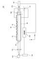
- FIG. 1 is a diagram showing a configuration of a polarization inversion processing device 100 according to the first embodiment, together with a ferroelectric crystal 10.
- the polarization inversion processing apparatus 100 includes a power source 110, a light source 120, a measurement unit 130, and a control unit 140, and is formed in a ferroelectric domain 10 in a periodically domain-inverted structure.
- a first electrode 20 is formed on the first surface of the ferroelectric crystal 10
- a second electrode 30 is formed on the second surface of the ferroelectric crystal 10 that faces the first surface.
- the power source 110 applies a voltage between the first electrode 20 and the second electrode 30.
- the light source 120 makes light incident on one of the two end faces (first end face: the left end face in FIG.
- This incident light includes a wavelength (first wavelength) whose wavelength is converted by the polarization inversion structure of the ferroelectric crystal 10.
- the measuring unit 130 reverses the polarization of the ferroelectric crystal 10 out of the light (radiated light) emitted from the other end surface in the first direction of the ferroelectric crystal 10 (second end surface: the right end surface in FIG. 1).
- the intensity of the wavelength component after wavelength conversion by the structure is measured.
- the control unit 140 determines the end timing of voltage application by the power source 110 based on the intensity measured by the measurement unit 130. Details will be described below.
- a portion of the conductive film 24 located in the opening of the insulating film 22 is the first electrode 20.
- the plurality of first electrodes 20 are connected to each other through a portion of the conductive film 24 located on the insulating film 22.
- the conductive film 24 is a metal film such as an Al film, and is formed using, for example, a sputtering method.
- the second electrode 30 is formed on the second surface (eg, -Z surface) of the ferroelectric crystal 10.
- the second electrode 30 is formed so as to face any of the plurality of first electrodes 20.
- the second electrode 30 is a metal film such as an Al film, and is formed using, for example, a sputtering method.
- a power source 110 is connected to the first electrode 20 and the second electrode 30.
- the power source 110 applies a voltage between the first electrode 20 and the second electrode 30.
- the power supply 110 is controlled by the control unit 140.
- the controller 140 controls the power supply 110 to apply a pulse waveform voltage to the first electrode 20 and the second electrode 30.
- the pulse waveform is rectangular, for example.
- the light source 120 is a laser light source, for example, and makes light incident on the first end face of the ferroelectric crystal 10. As described above, this light includes the first wavelength component.
- the first wavelength is a wavelength that is wavelength-converted by the polarization inversion structure of the ferroelectric crystal 10.
- the light emission of the light source 120 is controlled by the control unit 140.
- the control unit 140 causes the light source 120 to emit light while the power supply 110 applies a voltage to the first electrode 20 and the second electrode 30.
- the control unit 140 may cause the light source 120 to emit light in pulses.
- a wavelength filter 150 may be provided between the second end face of the ferroelectric crystal 10 and the measurement unit 130.
- the wavelength filter 150 passes light of the second wavelength and cuts light of other wavelengths (including the first wavelength).
- the wavelength filter 150 may be a filter that cuts light of the first wavelength.
- the control unit 140 controls the power supply 110 and the light source 120 using the measurement result of the measurement unit 130. Specifically, the control unit 140 ends the application of voltage to the first electrode 20 and the second electrode 30 by the power source 110 when the intensity of the second wavelength light detected by the measurement unit 130 reaches the reference value. To do. At this time, the control unit 140 also ends the operation of the light source 120.
- FIG. 2 is a graph showing an example of a detection result by the measurement unit 130.
- the horizontal axis represents the time t after the power supply 110 applies a voltage between the first electrode 20 and the second electrode 30.
- the detection value of the measurement unit 130 gradually increases during the initial period. This is because a domain-inverted region is formed in a region between the first electrode 20 and the second electrode 30 in the ferroelectric crystal 10, and this domain-inverted region expands with time t.
- the detection result of the measurement unit 130 is lowered. This is because the domain-inverted region of the ferroelectric crystal 10 is excessively widened and protrudes from the region sandwiched between the first electrode 20 and the second electrode 30, and the period of domain-inverted collapses.
- the control unit 140 terminates the operation of the power supply 110 when the measurement result of the measurement unit 130 reaches the reference value.
- the domain-inverted region of the ferroelectric crystal 10 can be within an appropriate range. That is, the domain-inverted regions can be periodically formed in the ferroelectric crystal 10 with high accuracy.
- FIG. 3 is a diagram illustrating a configuration of the polarization inversion processing device 100 according to the second embodiment.
- the polarization inversion processing device 100 according to the present embodiment has the same configuration as the polarization inversion processing device 100 according to the first embodiment except for the following points.
- an optical path control unit 122 is provided between the light source 120 and the ferroelectric crystal 10.
- the optical path controller 122 moves the incident position of the incident light on the first end face of the ferroelectric crystal 10 between the first surface and the second surface (y direction in FIG. 3).
- the optical path control unit 122 is a galvanometer mirror and a drive unit that rotates the galvanometer mirror.
- the light source 120 irradiates the galvanometer mirror with incident light. This incident light is reflected by the galvanometer mirror and enters the first end face of the ferroelectric crystal 10.
- the angle of the reflection surface of the galvanometer mirror with respect to the first end face of the ferroelectric crystal 10 gradually changes. Thereby, the incident position of the incident light on the first end face of the ferroelectric crystal 10 moves between the first surface and the second surface.
- the configuration of the optical path control unit 122 is not limited to the above example.
- the optical path control unit 122 changes the direction of the light source 120 to change the incident position of incident light on the first end face of the ferroelectric crystal 10 between the first surface and the second surface (y direction in FIG. 3). It may be moved.
- a lens 124 is provided between the optical path controller 122 and the first end face of the ferroelectric crystal 10, and a lens 126 is provided between the second end face of the ferroelectric crystal 10 and the wavelength filter 150. Is provided.
- the lens 124 aligns the light incident on the ferroelectric crystal 10 from the optical path control unit 122 in the first direction (x direction in FIG. 3).
- the lens 126 causes the radiated light emitted from the second end face of the ferroelectric crystal 10 to enter the wavelength filter 150 and the measurement unit 130.
- the polarization inversion of the ferroelectric crystal 10 is performed based on the measurement result by the measurement unit 130. An image showing the progress can be generated.
- the same effect as that of the first embodiment can be obtained.
- the incident position of the incident light on the first end face of the ferroelectric crystal 10 moves between the first surface and the second surface.
- the voltage application by the power source 110 can be terminated when almost the entire thickness direction is inverted. . Accordingly, the domain-inverted regions can be periodically formed in the ferroelectric crystal 10 with higher accuracy.
Landscapes
- Physics & Mathematics (AREA)
- Nonlinear Science (AREA)
- General Physics & Mathematics (AREA)
- Optics & Photonics (AREA)
- Optical Modulation, Optical Deflection, Nonlinear Optics, Optical Demodulation, Optical Logic Elements (AREA)
Abstract
電源(110)は、第1電極(20)と第2電極(30)の間に電圧を印加する。光源(120)は、強誘電体結晶(10)の第1方向(図1におけるx方向)における2つの端面の一方(第1端面:図1における左側の端面)に、光を入射する。この入射光には、強誘電体結晶(10)の分極反転構造によって波長変換される波長(第1波長)が含まれる。測定部(130)は、強誘電体結晶(10)の第1方向の他方の端面(第2端面:図1における右側の端面)から放射された光(放射光)のうち、強誘電体結晶(10)の分極反転構造によって波長変換された後の波長成分の強度を測定する。そして制御部(140)は、測定部(130)によって測定された強度に基づいて、電源(110)による電圧印加の終了タイミングを判断する。
Description
本発明は、強誘電体結晶に分極反転領域を形成する分極反転方法及び分極反転処理装置に関する。
強誘電体結晶に分極反転領域を周期的に形成することにより、疑似位相整合素子を形成することが行われている。疑似位相整合素子を用いると、光の波長を例えば短波長側に変換することができる。疑似位相整合素子において、分極反転領域の周期は、変換前の光の波長及び変換後の光の波長によって定まる。言い換えると、分極反転領域の周期は高い精度で管理される必要がある。
例えば特許文献1には、強誘電体結晶に分極反転領域を周期的に形成する方法が記載されている。この方法では、まず、強誘電体結晶の第1主表面に絶縁膜を形成する。そして、この絶縁膜に複数の開口を周期的に形成した後、この絶縁膜上及び開口内に位置する強誘電体結晶に第1電極を形成する。また、強誘電体結晶の第1主表面とは逆側の面に、第2電極を形成する。次いで、第1電極と第2電極の間に電圧を印加することにより、強誘電体結晶に分極反転領域を周期的に形成する。
強誘電体結晶に電圧を印加しておくと、強誘電体結晶のうち電圧が印加されている領域の分極は徐々に反転していく。そして電圧の印加時間が長くなると、分極反転領域は電圧が印加されている領域の周囲まで広がる。このため、強誘電体結晶に高い精度で分極反転領域を形成するためには、電圧の印加時間を適切な範囲に収める必要がある。一方、強誘電体結晶にはある程度のばらつきがあるため、上記した電圧の印加時間の適切な範囲は、個々の強誘電体結晶によって異なる。このため、強誘電体結晶に分極反転領域を周期的に形成する場合において、分極反転領域の精度を高めることは難しかった。
本発明は上記事情に鑑みてなされたものであり、その目的とするところは、強誘電体結晶に分極反転領域を周期的に形成する場合において、分極反転領域の精度を高めることにある。
本発明において、強誘電体結晶の第1面には、複数の第1電極が第1方向に互いに離して配置される。また、強誘電体結晶の第1面に対向する第2面には、第2電極が複数の第1電極に対向するように配置される。そして、強誘電体結晶に分極反転構造を形成するために、第1電極と第2電極の間に電圧を印加する。ここで、電圧を印加しながら、強誘電体結晶の第1方向の第1端面から、第1波長の光を有する入射光を入射する。第1波長の光は、上記した分極反転構造によって波長変換される。また、強誘電体結晶の第1端面に対向する第2端面から放射された放射光のうち、上記した分極反転構造によって波長変換された後の波長の強度を測定する。そして、この強度に基づいて、電圧印加の終了タイミングを判断する。
本発明によれば、強誘電体結晶に分極反転領域を周期的に形成する場合において、分極反転領域の精度を高めることができる。
上述した目的、およびその他の目的、特徴および利点は、以下に述べる好適な実施の形態、およびそれに付随する以下の図面によってさらに明らかになる。
以下、本発明の実施の形態について、図面を用いて説明する。尚、すべての図面において、同様な構成要素には同様の符号を付し、適宜説明を省略する。
(第1の実施形態)
図1は、第1の実施形態に係る分極反転処理装置100の構成を、強誘電体結晶10とともに示す図である。本実施形態に係る分極反転処理装置100は、電源110、光源120、測定部130、及び制御部140を備え、強誘電体結晶10に周期的な分極反転構造に形成する。強誘電体結晶10の第1面には第1電極20が形成されており、強誘電体結晶10のうち第1面に対向する第2面には第2電極30が形成されている。電源110は、第1電極20と第2電極30の間に電圧を印加する。光源120は、強誘電体結晶10の第1方向(図1におけるx方向)における2つの端面の一方(第1端面:図1における左側の端面)に、光を入射する。この入射光には、強誘電体結晶10の分極反転構造によって波長変換される波長(第1波長)が含まれる。測定部130は、強誘電体結晶10の第1方向の他方の端面(第2端面:図1における右側の端面)から放射された光(放射光)のうち、強誘電体結晶10の分極反転構造によって波長変換された後の波長成分の強度を測定する。そして制御部140は、測定部130によって測定された強度に基づいて、電源110による電圧印加の終了タイミングを判断する。以下、詳細に説明する。
図1は、第1の実施形態に係る分極反転処理装置100の構成を、強誘電体結晶10とともに示す図である。本実施形態に係る分極反転処理装置100は、電源110、光源120、測定部130、及び制御部140を備え、強誘電体結晶10に周期的な分極反転構造に形成する。強誘電体結晶10の第1面には第1電極20が形成されており、強誘電体結晶10のうち第1面に対向する第2面には第2電極30が形成されている。電源110は、第1電極20と第2電極30の間に電圧を印加する。光源120は、強誘電体結晶10の第1方向(図1におけるx方向)における2つの端面の一方(第1端面:図1における左側の端面)に、光を入射する。この入射光には、強誘電体結晶10の分極反転構造によって波長変換される波長(第1波長)が含まれる。測定部130は、強誘電体結晶10の第1方向の他方の端面(第2端面:図1における右側の端面)から放射された光(放射光)のうち、強誘電体結晶10の分極反転構造によって波長変換された後の波長成分の強度を測定する。そして制御部140は、測定部130によって測定された強度に基づいて、電源110による電圧印加の終了タイミングを判断する。以下、詳細に説明する。
強誘電体結晶10は、例えばMgを添加したLiNbO3(ニオブ酸リチウム)単結晶基板であるが、LiTaO3(タンタル酸リチウム)などの他の強誘電体からなる結晶であってもよい。強誘電体結晶10の第1面(例えば+Z面)には、複数の第1電極20が第1方向(図1におけるx方向)に互いに離間して配置されている。これら複数の第1電極20は、電気的に接続されている。
本図に示す例では、強誘電体結晶10の第1面には絶縁膜22が形成されている。絶縁膜22は、例えば酸化アルミニウムや酸化ジルコニウムなどの金属酸化物、酸化シリコンなどの無機酸化物、又は窒化シリコンなどの窒素化合物である。絶縁膜22は、例えばスパッタリング法、真空蒸着法、またはCVD法などを用いて形成される。絶縁膜22には複数の開口が第1方向に互いに離間して配置されている。そして絶縁膜22上及び絶縁膜22の開口内には、導電膜24が形成されている。導電膜24のうち絶縁膜22の開口内に位置する部分が第1電極20となっている。そして複数の第1電極20は、導電膜24のうち絶縁膜22の上に位置する部分を介して、互いに接続している。導電膜24は、例えばAl膜などの金属膜であり、例えばスパッタリング法を用いて形成されている。
また、強誘電体結晶10の第2面(例えば-Z面)には、第2電極30が形成されている。第2電極30は、複数の第1電極20のいずれにも対向するように形成されている。第2電極30は、例えばAl膜などの金属膜であり、例えばスパッタリング法を用いて形成されている。
第1電極20及び第2電極30には、電源110が接続している。電源110は、第1電極20及び第2電極30の間に電圧を印加する。電源110は、制御部140によって制御されている。制御部140は、電源110を制御することにより、第1電極20及び第2電極30に、パルス波形の電圧を印加する。パルス波形は、例えば矩形である。
光源120は、例えばレーザ光源であり、強誘電体結晶10の第1端面に光を入射する。この光には、上記したように、第1波長の成分が含まれる、第1波長は、強誘電体結晶10の分極反転構造によって波長変換される波長である。光源120の発光は、制御部140によって制御されている。例えば制御部140は、電源110が第1電極20及び第2電極30に電圧を印加している間、光源120を発光させる。ここで制御部140は、光源120をパルス的に発光させてもよい。
測定部130は、フォトダイオードなどの光電変換素子を有しており、強誘電体結晶10の第2端面から放射された放射光を光電変換する。測定部130が有する光電変換素子は、放射光のうち、第1波長が強誘電体結晶10の分極反転構造によって波長変換された後の波長(第2波長)を光電変換する。このようにするためには、光電変換素子は、第2波長における光電変換効率が特に高いのが好ましい。
また、強誘電体結晶10の第2端面と測定部130の間に、波長フィルタ150を設けてもよい。波長フィルタ150は、第2波長の光を通し、その他の波長(第1波長を含む)の光をカットする。なお、波長フィルタ150は、第1波長の光をカットするフィルタであってもよい。波長フィルタ150を設けることにより、測定部130は、高い精度で第2波長の光の強度を測定することができる。
制御部140は、測定部130の測定結果を用いて、電源110及び光源120を制御する。具体的には、制御部140は、測定部130が検出した第2波長の光の強度が基準値になった時に、電源110による第1電極20及び第2電極30への電圧の印加を終了する。このとき、制御部140は、光源120の動作も終了させる。
図2は、測定部130による検出結果の一例を示すグラフである。本図に示す例において、横軸は、電源110が第1電極20及び第2電極30の間に電圧を印加してからの時間tである。本図に示すように、第1電極20及び第2電極30の間に電圧していると、初期の間は徐々に測定部130の検出値が増加していく。これは、強誘電体結晶10のうち第1電極20と第2電極30に挟まれている領域に分極反転領域が形成され、かつこの分極反転領域が時間tとともに広がっていくためである。ただし、時間tが長くなりすぎると、測定部130の検出結果は低下してしまう。これは、強誘電体結晶10の分極反転領域が広がりすぎ、第1電極20と第2電極30に挟まれた領域からはみ出てしまい、分極反転の周期が崩れるためである。
これに対して本実施形態では、制御部140は、測定部130の測定結果が基準値に達したときに、電源110の動作を終了させる。このため、強誘電体結晶10の分極反転領域を適切な範囲に収めることができる。すなわち、強誘電体結晶10に、高い精度で分極反転領域を周期的に形成することができる。
(第2の実施形態)
図3は、第2の実施形態に係る分極反転処理装置100の構成を示す図である。本実施形態に係る分極反転処理装置100は、以下の点を除いて、第1の実施形態に係る分極反転処理装置100と同様の構成である。
図3は、第2の実施形態に係る分極反転処理装置100の構成を示す図である。本実施形態に係る分極反転処理装置100は、以下の点を除いて、第1の実施形態に係る分極反転処理装置100と同様の構成である。
まず、光源120と強誘電体結晶10の間には、光路制御部122が設けられている。光路制御部122は、強誘電体結晶10の第1端面における入射光の入射位置を、第1面と第2面の間(図3におけるy方向)で移動させる。本図に示す例では、光路制御部122はガルバノミラー及びこれを回転させる駆動部である。光源120は、ガルバノミラーに入射光を照射する。この入射光は、ガルバノミラーによって反射され、強誘電体結晶10の第1端面に入射する。この際、強誘電体結晶10の第1端面に対するガルバノミラーの反射面の角度は徐々に変化する。これにより、強誘電体結晶10の第1端面における入射光の入射位置は、第1面と第2面の間で移動する。
なお、光路制御部122の構成は上記した例に限定されない。例えば光路制御部122は、光源120の向きを変えることにより、強誘電体結晶10の第1端面における入射光の入射位置を、第1面と第2面の間(図3におけるy方向)で移動させてもよい。
また、光路制御部122と強誘電体結晶10の第1端面の間には、レンズ124が設けられており、強誘電体結晶10の第2端面と波長フィルタ150の間には、レンズ126が設けられている。レンズ124は、光路制御部122から強誘電体結晶10に入射する光を、第1方向(図3におけるx方向)に揃える。一方、レンズ126は、強誘電体結晶10の第2端面から放射される放射光を、波長フィルタ150及び測定部130に入射させる。
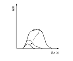
図4は、測定部130による検出結果の一例を示すグラフである。本図に示す例において、横軸は、強誘電体結晶10の第1面からの深さd(図3参照)である。このグラフは、強誘電体結晶10の厚さ方向に分極反転がどの程度進んでいるかを示している。そして図4において点線で示すように、このグラフは、一定間隔で生成される。制御部140は、d方向においてほぼ全域で測定部130による検出結果が基準値以上になった時に、電源110による電圧印加を終了させる。
なお、入射光をさらに強誘電体結晶10の幅方向(図3の紙面に対して垂直な方向)に移動させると、測定部130による測定結果に基づいて、強誘電体結晶10の分極反転の進行状況を示す画像を生成することができる。
本実施形態によっても、第1の実施形態と同様の効果が得られる。また、光路制御部122を設けることにより、強誘電体結晶10の第1端面における入射光の入射位置は、第1面と第2面の間で移動する。これにより、強誘電体結晶10の厚さ方向(図3におけるd方向)において、どの領域の分極反転が進んでいるかを確認することができる。そして、強誘電体結晶10のうち第1電極20及び第2電極30で挟まれている領域において、厚さ方向のほぼ全体が分極反転したときに、電源110による電圧印加を終了させることができる。従って、さらに高い精度で、強誘電体結晶10に分極反転領域を周期的に形成することができる。
以上、図面を参照して本発明の実施形態について述べたが、これらは本発明の例示であり、上記以外の様々な構成を採用することもできる。
この出願は、2014年8月5日に出願された日本出願特願2014-159371号を基礎とする優先権を主張し、その開示の全てをここに取り込む。
Claims (4)
- 強誘電体結晶の第1面に、複数の第1電極を第1方向に互いに離して配置し、かつ、前記強誘電体結晶のうち前記第1面に対向する第2面に、第2電極を前記複数の第1電極に対向するように配置し、
前記強誘電体結晶に分極反転構造を形成するために、前記第1電極と前記第2電極の間に電圧を印加し、
前記電圧を印加しながら、前記強誘電体結晶の第1方向の第1端面から、前記分極反転構造によって波長変換される第1波長の光を有する入射光を入射し、かつ前記強誘電体結晶の前記第1端面に対向する第2端面から放射された放射光のうち、前記分極反転構造によって波長変換された後の波長の強度を測定し、当該強度に基づいて、前記電圧の印加の終了タイミングを判断する、分極反転方法。 - 請求項1に記載の分極反転方法において
前記第1端面における前記入射光の入射位置を、前記第1面と前記第2面の間で移動させる分極反転方法。 - 請求項1又は2に記載の分極反転方法において、
前記第2端面と、前記放射光を測定する測定部の間に、前記第1波長の光をカットする波長フィルタを配置する分極反転方法。 - 強誘電体結晶の第1面に形成された第1電極と、前記強誘電体結晶のうち前記第1面に対向する第2面に形成された第2電極の間に、前記強誘電体結晶に分極反転構造を形成するために電圧を印加する電源と、
前記強誘電体結晶の第1方向の第1端面から、前記分極反転構造によって波長変換される第1波長の光を有する入射光を入射する光源と、
前記強誘電体結晶の前記第1端面に対向する第2端面から放射された放射光のうち、前記分極反転構造によって波長変換された後の波長成分の強度を測定する測定部と、
前記強度に基づいて、前記電圧印加の終了タイミングを判断する制御部と、
を備える分極反転処理装置。
Applications Claiming Priority (2)
| Application Number | Priority Date | Filing Date | Title |
|---|---|---|---|
| JP2014-159371 | 2014-08-05 | ||
| JP2014159371A JP2017167170A (ja) | 2014-08-05 | 2014-08-05 | 分極反転方法及び分極反転処理装置 |
Publications (1)
| Publication Number | Publication Date |
|---|---|
| WO2016021272A1 true WO2016021272A1 (ja) | 2016-02-11 |
Family
ID=55263551
Family Applications (1)
| Application Number | Title | Priority Date | Filing Date |
|---|---|---|---|
| PCT/JP2015/064556 Ceased WO2016021272A1 (ja) | 2014-08-05 | 2015-05-21 | 分極反転方法及び分極反転処理装置 |
Country Status (3)
| Country | Link |
|---|---|
| JP (1) | JP2017167170A (ja) |
| TW (1) | TW201617751A (ja) |
| WO (1) | WO2016021272A1 (ja) |
Citations (2)
| Publication number | Priority date | Publication date | Assignee | Title |
|---|---|---|---|---|
| JP2009092712A (ja) * | 2007-10-03 | 2009-04-30 | Sony Corp | 光機能素子の製造方法及びタンタル酸リチウム単結晶の製造方法 |
| JP2011043604A (ja) * | 2009-08-20 | 2011-03-03 | Oki Electric Industry Co Ltd | 周期的分極反転構造の形成方法 |
-
2014
- 2014-08-05 JP JP2014159371A patent/JP2017167170A/ja active Pending
-
2015
- 2015-05-21 WO PCT/JP2015/064556 patent/WO2016021272A1/ja not_active Ceased
- 2015-07-29 TW TW104124542A patent/TW201617751A/zh unknown
Patent Citations (2)
| Publication number | Priority date | Publication date | Assignee | Title |
|---|---|---|---|---|
| JP2009092712A (ja) * | 2007-10-03 | 2009-04-30 | Sony Corp | 光機能素子の製造方法及びタンタル酸リチウム単結晶の製造方法 |
| JP2011043604A (ja) * | 2009-08-20 | 2011-03-03 | Oki Electric Industry Co Ltd | 周期的分極反転構造の形成方法 |
Non-Patent Citations (2)
| Title |
|---|
| M.J.MISSEY ET AL.: "Real-time visualization of domain formation inperiodically poled lithium niobate", OPTICS EXPRESS, vol. 6, no. 10, 8 May 2000 (2000-05-08), pages 186 - 195 * |
| N.E. YU ET AL.: "In-situ Visualization Method of Domain Boundaryfor Stoichiometric Lithium Niobate Crystal", JAPANESE JOURNAL OF APPLIED PHYSICS, vol. 48, 21 December 2009 (2009-12-21), pages 121407 - 1 - 121407-4 * |
Also Published As
| Publication number | Publication date |
|---|---|
| TW201617751A (zh) | 2016-05-16 |
| JP2017167170A (ja) | 2017-09-21 |
Similar Documents
| Publication | Publication Date | Title |
|---|---|---|
| US11385334B2 (en) | Optical scanning element | |
| JP2013140328A (ja) | 光学装置、光偏向装置及び光変調装置 | |
| JP6115013B2 (ja) | 光偏向装置、レーザレーダ装置 | |
| JP2010020135A (ja) | 波長変換装置、レーザ光発生装置および波長変換方法 | |
| JPWO2009107473A1 (ja) | 波長変換素子 | |
| WO2016021272A1 (ja) | 分極反転方法及び分極反転処理装置 | |
| TW201413359A (zh) | 波長變換元件、光源裝置及波長變換元件之製造方法 | |
| CN101535887A (zh) | 光波导基板的制造方法 | |
| JP4806427B2 (ja) | 波長変換素子およびその製造方法 | |
| US10018889B2 (en) | Acousto-optic deflector comprising multiple electro-acoustic transducers | |
| JP5992346B2 (ja) | 波長変換素子の製造方法 | |
| US8820968B2 (en) | Wavelength conversion element, laser light source device, image display device, and method of manufacturing wavelength conversion element | |
| JP6508084B2 (ja) | 波長変換光学装置及びレーザ装置 | |
| CN103337784B (zh) | 一种基于偏振光回馈的激光偏振态控制方法 | |
| JP6059627B2 (ja) | 光偏向器および光偏向器の制御方法 | |
| JP6102432B2 (ja) | 光変調器 | |
| JP6322883B2 (ja) | 光偏向素子 | |
| JPH05188421A (ja) | 光波長変換装置 | |
| JP4577718B2 (ja) | 分極反転構造を作成する装置及び分極反転構造の作成方法 | |
| JP5403521B2 (ja) | 分極反転領域を形成する装置 | |
| JP2004054191A (ja) | 光学素子の角度調整装置及び角度調整方法 | |
| JP6446518B2 (ja) | 波長変換素子の製造方法 | |
| SU797378A1 (ru) | Акустооптическое устройство дл управлени оптическим излучением | |
| JP5923885B2 (ja) | パルスレーザ発振器及びパルスレーザ発振制御方法 | |
| Bakunov et al. | Asymmetric Cherenkov Radiation for Improving Terahertz Emission from the Si-prism-coupled LiNbO3 layer |
Legal Events
| Date | Code | Title | Description |
|---|---|---|---|
| 121 | Ep: the epo has been informed by wipo that ep was designated in this application |
Ref document number: 15830007 Country of ref document: EP Kind code of ref document: A1 |
|
| NENP | Non-entry into the national phase |
Ref country code: DE |
|
| NENP | Non-entry into the national phase |
Ref country code: JP |
|
| 122 | Ep: pct application non-entry in european phase |
Ref document number: 15830007 Country of ref document: EP Kind code of ref document: A1 |